CN101584002B - Memory system and computer memory system - Google Patents
Memory system and computer memory systemDownload PDFInfo
- Publication number
- CN101584002B CN101584002BCN200880002092XACN200880002092ACN101584002BCN 101584002 BCN101584002 BCN 101584002BCN 200880002092X ACN200880002092X ACN 200880002092XACN 200880002092 ACN200880002092 ACN 200880002092ACN 101584002 BCN101584002 BCN 101584002B
- Authority
- CN
- China
- Prior art keywords
- bit line
- memory
- sense amplifier
- transient
- current
- Prior art date
- Legal status (The legal status is an assumption and is not a legal conclusion. Google has not performed a legal analysis and makes no representation as to the accuracy of the status listed.)
- Expired - Fee Related
Links
Images


Classifications
- G—PHYSICS
- G11—INFORMATION STORAGE
- G11C—STATIC STORES
- G11C16/00—Erasable programmable read-only memories
- G11C16/02—Erasable programmable read-only memories electrically programmable
- G11C16/06—Auxiliary circuits, e.g. for writing into memory
- G11C16/26—Sensing or reading circuits; Data output circuits
- G11C16/28—Sensing or reading circuits; Data output circuits using differential sensing or reference cells, e.g. dummy cells
Landscapes
- Read Only Memory (AREA)
- Dram (AREA)
Abstract
Translated fromChinese
Description
Translated fromChinese技术领域technical field
本发明涉及计算机系统,且更明确地说,涉及存储器系统。 The present invention relates to computer systems, and more particularly, to memory systems. the
背景技术Background technique
例如快闪存储器系统等存储器系统在读取操作中利用读出放大器来从存储器单元读取数据,其中给定存储器单元的状态由所述存储器单元在明确界定的偏置条件下所吸收的电流的量决定。在最简单的情况下,存储元件可处于两种状态:“0”状态或“1”状态。在“0”状态下,存储元件不吸收电流,且在“1”状态下,存储元件吸收电流。存储元件可为(例如)单个快闪存储器单元(如在“或非”快闪存储器中)或串(如在“与非”快闪存储器中)。串通常是具有一连串单个快闪存储器单元(例如,8个、16个或更多快闪存储器单元)的存储元件。 Memory systems, such as flash memory systems, utilize sense amplifiers to read data from memory cells during a read operation, where the state of a given memory cell is determined by a function of the current drawn by the memory cell under well-defined bias conditions. volume decision. In the simplest case, a storage element can be in two states: a "0" state or a "1" state. In the "0" state, the storage element sinks no current, and in the "1" state, the storage element sinks current. A storage element can be, for example, a single flash memory cell (as in NOR flash memory) or a string (as in NAND flash memory). A string is typically a storage element having a series of individual flash memory cells (eg, 8, 16 or more flash memory cells). the
一些快闪存储器系统的问题在于它们可能由于读出放大器处的低电流电平而不允许快速随机存取时间。利用“与非”架构的快闪存储器尤其如此。由于与将存储元件连接到读出放大器的存储器矩阵位线相关联的瞬变电流而出现另一问题。“与非”架构对于此问题来说再次是尤其严重的,因为“与非”结构通常是以非常大的存储器矩阵建置而成,且因此具有非常长的位线。瞬变电流是有问题的,因为瞬变电流被加到用于确定存储器单元状态的存储器单元电流和参考电流。错误的存储器单元电流和参考电流读数可因此导致错误的读取操作。 A problem with some flash memory systems is that they may not allow fast random access times due to the low current levels at the sense amplifiers. This is especially true for flash memory utilizing a NAND architecture. Another problem arises due to the transient currents associated with the memory matrix bit lines connecting the storage elements to the sense amplifiers. This problem is again particularly acute for NAND architectures because NAND structures are typically built with very large memory matrices, and thus have very long bit lines. Transient currents are problematic because they are added to the memory cell current and reference current used to determine the state of the memory cell. False memory cell current and reference current readings can thus lead to erroneous read operations. the
因此,需要一种经改进的存储器系统。本发明解决此需要。 Therefore, there is a need for an improved memory system. The present invention addresses this need. the
发明内容Contents of the invention
本发明揭示一种存储器系统。在一个实施例中,所述存储器系统包含第一位线,其中所述第一位线产生第一瞬变电流。所述存储器系统还包含耦合到所述第一位线的读出放大器。存储器系统还包含耦合到读出放大器的第二位线,其中所述第二位线产生第二瞬变电流,所述第二瞬变电流等于所述第一瞬变电流。读出放大器使所述第一和第二瞬变电流能够抵消。 The invention discloses a memory system. In one embodiment, the memory system includes a first bit line, wherein the first bit line generates a first transient current. The memory system also includes a sense amplifier coupled to the first bit line. The memory system also includes a second bit line coupled to the sense amplifier, wherein the second bit line generates a second transient current equal to the first transient current. A sense amplifier enables cancellation of the first and second transient currents. the
根据本文所揭示的系统,可在不受瞬变电流不利地影响的情况下,确定存储器单元的状态。 According to the systems disclosed herein, the state of a memory cell can be determined without being adversely affected by transient currents. the
附图说明Description of drawings
图1是根据一个实施例的快闪存储器电路的示意图。 FIG. 1 is a schematic diagram of a flash memory circuit according to one embodiment. the
图2是展示根据一个实施例的存储器系统的框图。 Figure 2 is a block diagram showing a memory system according to one embodiment. the
图3是根据另一实施例的存储器系统的框图。 Figure 3 is a block diagram of a memory system according to another embodiment. the
图4A说明根据一个实施例的图3的存储器系统的操作。 Figure 4A illustrates the operation of the memory system of Figure 3, according to one embodiment. the
图4B说明根据另一实施例的图3的存储器系统的操作。 Figure 4B illustrates the operation of the memory system of Figure 3 according to another embodiment. the
图5A说明根据一个实施例的图3的存储器系统的操作。 Figure 5A illustrates the operation of the memory system of Figure 3, according to one embodiment. the
图5B说明根据另一实施例的图3的存储器系统的操作。 Figure 5B illustrates the operation of the memory system of Figure 3 according to another embodiment. the
具体实施方式Detailed ways
本发明涉及计算机系统,且更明确地说,涉及存储器系统。呈现以下描述内容以使所属领域的技术人员能够制作和使用本发明,且以下描述内容是在专利申请案及其要求的上下文中提供的。对本文所描述的优选实施例以及一般原理和特征的各种修改对所属领域的技术人员来说将是显而易见的。因此,本发明无意限于所展示的实施例,而是将被赋予与本文所描述的原理和特征一致的最宽范围。 The present invention relates to computer systems, and more particularly, to memory systems. The following description is presented to enable any person skilled in the art to make and use the invention, and is provided in the context of a patent application and its claims. Various modifications to the preferred embodiment, and the general principles and features described herein will be readily apparent to those skilled in the art. Thus, the present invention is not intended to be limited to the embodiments shown but is to be accorded the widest scope consistent with the principles and features described herein. the
揭示一种存储器系统。在一个实施例中,所述存储器系统利用虚拟存储器位线来产生瞬变电流,所述瞬变电流抵消与所寻址的存储器位线相关联的任何瞬变电流。类似地,存储器系统利用虚拟参考位线来产生瞬变电流,所述瞬变电流抵消与所寻址的参考位线相关联的任何瞬变电流。虚拟存储器位线、所寻址的存储器位线、虚拟参考位线和所寻址的参考位线耦合到同一读出放大器,以使瞬变电流能够被抵消。因此,可基于存储器位线电流与参考位线电流之间的差异确定与所寻址的存储器位线相关联的给定存储器单元的状态,而不会受瞬变电流不利地影响。为了更明确地描述本发明的特征,现在结合附图而参考以下描述。 A memory system is disclosed. In one embodiment, the memory system utilizes dummy memory bit lines to generate transient currents that counteract any transient currents associated with the addressed memory bit lines. Similarly, memory systems utilize virtual reference bit lines to generate transient currents that counteract any transient currents associated with addressed reference bit lines. The dummy memory bit line, the addressed memory bit line, the dummy reference bit line and the addressed reference bit line are coupled to the same sense amplifier so that transient currents can be cancelled. Accordingly, the state of a given memory cell associated with an addressed memory bit line can be determined based on the difference between the memory bit line current and the reference bit line current without being adversely affected by the transient current. In order to more specifically describe the features of the present invention, reference is now made to the following description taken in conjunction with the accompanying drawings. the
尽管在“与非”快闪存储器的上下文中描述本文所揭示的本发明,但本发明可应用于其它类型的存储器,例如“或非”存储器和存储器架构,且仍在本发明的精神和范围内。 Although the invention disclosed herein is described in the context of NAND flash memory, the invention can be applied to other types of memory, such as NOR memory and memory architectures, and remain within the spirit and scope of the invention Inside. the
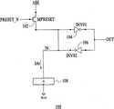
图1是根据一个实施例的快闪存储器电路100的示意图。快闪存储器电路包含晶体管102、反相器104和106以及“与非”串108,“与非”串108是一连串快闪存储器单元。如图1展示,在“与非”快闪存储器中,通常通过将串108链接到双稳态锁存电路(即,反相器104和106)的输入节点,来执行读取操作。 FIG. 1 is a schematic diagram of a
在读取操作开始之前,控制信号PRESET_N将快闪存储器电路100的输出电平OUT预设为两个稳定状态中的一者(例如,“0”或“1”)。一旦读取操作开始,如果串电流 为零,那么锁存输出OUT保持在预设值。如果串电流为正,那么串电流将锁存输入IN处的电压至少放电到反相器104的触发电平,使得锁存输出可切换到相反状态。由于串所包含的一系列快闪存储器单元的缘故,串电流可能非常低。因此,锁存输入节点无法被非常快速地放电。由于此缘故,“与非”架构通常不允许快速随机存取时间。相反,单个读出放大器仅具有简单的锁存电路。因此,有可能设计非常高密度的读出放大器来在非常高数目的串上同时执行读取操作,从而在初始等待时间后获得非常高的数据通过量。 The control signal PRESET_N presets the output level OUT of the
用于提供较快读取操作的一种方法是使用更复杂且因此通常更大的读出放大器。举例来说,在电流比较读出放大器中,通过将给定存储元件处的电流(或存储器单元电流Icell)与参考电流(Iref)进行比较,来执行读取操作,所述参考电流具有通常位于逻辑状态“1”下的存储器单元电流值与逻辑状态“0”下的存储器单元电流值之间的值。读出放大器通常读取所述两个电流之间的差,且接着将所述差转换成电压信号。 One approach for providing faster read operations is to use more complex and thus usually larger sense amplifiers. For example, in a current comparison sense amplifier, a read operation is performed by comparing the current at a given memory element (or memory cell current Icell ) with a reference current (Iref ) having Typically a value between the memory cell current value at logic state "1" and the memory cell current value at logic state "0". A sense amplifier typically reads the difference between the two currents and then converts the difference into a voltage signal.
图2是展示根据一个实施例的存储器系统200的框图。存储器系统200包含具有存储器位线204的矩阵202、列解码器206、读出放大器208和参考产生器210。参考产生器210产生参考电流。或者,参考电流可能由另一快闪存储器单元产生,以便跟踪存储器单元的过程特性。参考产生器210可相对于读出放大器208位于各种位置中。存储器位线204为物理列,其将属于其的单元的漏极连接在一起。为便于说明,仅展示一个存储器位线204。每一位线204耦合到列解码器206,列解码器206将所寻址的位线(即,所寻址的存储器单元)耦合到读出放大器208。 FIG. 2 is a block diagram showing a
一旦读取操作开始,读取路径的节点处的电压电平就调节到适当的偏置条件,以便允许给定存储器单元传导其合适的电流。举例来说,读出放大器可使所寻址的单元偏置,以使其漏极升高到所要的电压值。在一个实施例中,将存储器单元的漏极耦合到读出放大器的对应位线可被视为RC网络,其应升高到同一电压电平。所需的电流可由读出放大器供应,且电流穿过存储器单元电流所来自的同一路径。 Once a read operation begins, the voltage levels at the nodes of the read path are adjusted to appropriate bias conditions in order to allow a given memory cell to conduct its appropriate current. For example, a sense amplifier can bias the addressed cell so that its drain is raised to a desired voltage value. In one embodiment, the corresponding bit line that couples the drain of the memory cell to the sense amplifier can be viewed as an RC network that should be boosted to the same voltage level. The required current can be supplied by the sense amplifier, and the current passes through the same path that the memory cell current comes from. the
在初始瞬变周期期间,读出放大器读取存储器单元处的电流(Icell),以及被称为存储器位线预充电电流的瞬变电流。在此瞬变周期期间,存储器位线预充电电流通常达到峰值(通常大于存储器单元电流),且接着一旦存储器单元被合适地偏置,就降到零。预充电电流只是可影响存储器路径和参考路径两者的可能瞬变电流的一个实例。另一瞬变行为可(例如)与用以使所寻址的单元的栅极极化的时间等有关。因此,瞬变电流可包含来自存储器单元的任何可能的瞬变电流Itran,cell和/或来自参考位线的瞬变电流Itran,ref。 During the initial transient period, the sense amplifier reads the current at the memory cell (Icell ), and a transient current called the memory bit line precharge current. During this transient period, the memory bit line precharge current typically peaks (usually greater than the memory cell current) and then falls to zero once the memory cell is properly biased. Precharge current is just one example of possible transient currents that can affect both the memory path and the reference path. Another transient behavior may, for example, be related to the time to polarize the gate of the addressed cell, etc. Thus, the transient current may include any possible transient current Itran,cell from the memory cell and/or Itran,ref from the reference bit line.
在瞬变周期期间,读出放大器不仅可读取差(例如,Icell-Iref),而且可读取所有电流贡献的和(例如,Icell+Itran,cell-Iref-Itran,ref)。所述两个瞬变分量可大于存储器单元电流和参考电流两者。此外,由于参考电流路径相对于存储器电流路径可非常不同,因此两个分量Itran,cell和Itran,ref相对于彼此可非常不同。这可能使读取操作的性能显著恶化,因为正确地读取数据的唯一方式是等待,直到两个瞬变电流相对于差(Icell-Iref)为可忽略为止。遗憾的是,等待可能花费太多时间,从而危及性能,尤其是在单元电流非常小且较长的位线将存储器单元连接到列解码器的情况下。 During the transient period, the sense amplifier can read not only the difference (e.g., Icell −Iref ), but also the sum of all current contributions (e.g., Icell +Itran, cell −Iref −Itran, ref ). The two transient components can be greater than both the memory cell current and the reference current. Furthermore, since the reference current path can be very different relative to the memory current path, the two components Itran,cell and Itran,ref can be very different relative to each other. This can significantly worsen the performance of the read operation, since the only way to correctly read the data is to wait until the two transient currents are negligible relative to the difference (Icell -Iref ). Unfortunately, waiting can take too much time, jeopardizing performance, especially if the cell current is very low and long bit lines connect the memory cells to the column decoders.
另一重要问题与参考电流的静态值(即,最终值)有关。无论参考块放置在什么地方,均应将参考电流从参考块供应到读出放大器。这意味着一些电路(例如镜像连接的晶体管)需要将参考电流转移到读出放大器电池。遗憾的是,此操作可能受由镜像电路晶体管中的失配和通道长度调制误差导致的误差影响。在存储器单元电流和参考电流非常小的情况下,此问题尤其重要。事实上,电流误差不可相对于绝对参考电流值而忽略,因而严重地影响供应到读出放大器的参考电流的最终值。因此,合适的数据读取所依赖的静态电流差(Icell-Iref)可能非常不同,从而导致错误的读取。 Another important issue is related to the static value (ie final value) of the reference current. No matter where the reference block is placed, the reference current should be supplied from the reference block to the sense amplifier. This means that some circuitry (such as mirror-connected transistors) needs to divert the reference current to the sense amplifier battery. Unfortunately, this operation can be affected by errors caused by mismatches in the mirror circuit transistors and channel length modulation errors. This issue is especially important where the memory cell current and reference current are very small. In fact, the current error is not negligible with respect to the absolute reference current value, thus seriously affecting the final value of the reference current supplied to the sense amplifier. Therefore, the quiescent current difference (Icell −Iref ) upon which a proper data read depends may be very different, resulting in false reads.
最后,此架构具有涉及静态(最终参考电流值)和动态(参考和存储器瞬变电流)行为两者的一些问题。关于动态行为,避免瞬变电流的问题的唯一方式是等待,直到它们相对于电流差(Icell-Iref)变为可忽略为止。遗憾的是,这相对于电流目标读取性能可能花费太多时间。关于静态误差,其可能改变数据获取所依赖的电流差值(Icell-Iref)。 Finally, this architecture has some issues related to both static (final reference current value) and dynamic (reference and memory transient current) behavior. Regarding the dynamic behavior, the only way to avoid problems with transient currents is to wait until they become negligible with respect to the current difference (Icell -Iref ). Unfortunately, this can take too much time relative to the current target read performance. Regarding the static error, it may change the current difference (Icell −Iref ) on which the data acquisition depends.
在一个实施例中,图2的存储器系统200可用于获得对“与非”存储器的快速随机存取时间。然而,此架构应适合于“与非”存储器情形,其中存储器串电流包含于读出放大器操作中。首先,为了执行电流比较,需要用于“与非”情况的参考电流。在一个实施例中,参考产生器210可用于产生参考电流。然而,通过此途径,参考电流具有相对于存储器串电流完全独立的一些特性。 In one embodiment, the
存储器系统200可能具有次最佳的静态和动态行为,且在存储元件电流为低且其相关联的存储器位线较长时可能欠佳地执行。“与非”存储器通常被设计有非常大的阵列尺寸,且因此具有非常长的存储器位线。
优选途径是产生更适合所述实施例的目的的参考电流。首先,具有可跟踪存储器串的过程特性的参考电流是重要的。因此,如下文结合图3更详细地描述,参考串可用于产生参考电流。在一个实施例中,特殊参考串可操作以吸收具有在存储器串处于“1”状态和“0”状态时的存储器串电流的值之间的值的电流。举例来说,如果存储器串处于“0”状态,且因此不吸收电流,那么参考串可吸收“1”状态下的存储器串电流值的 一半。因此,在一个实施例中,参考串可具有相对于存储器串中的存储器单元的数目为两倍的数目的存储器单元。或者,参考串可与存储器串具有相同数目的存储器单元,其中具有一些过编程的单元。 The preferred approach is to generate a reference current that is more suitable for the purposes of the described embodiments. First, it is important to have a reference current that can track the process characteristics of the memory string. Thus, as described in more detail below in connection with FIG. 3 , a reference string can be used to generate a reference current. In one embodiment, a particular reference string is operable to sink a current having a value between the values of the memory string current when the memory string is in a "1" state and a "0" state. For example, if the memory string is in the "0" state, and therefore not sinking current, the reference string can sink half the current value of the memory string in the "1" state. Thus, in one embodiment, a reference string may have twice the number of memory cells relative to the number of memory cells in the memory string. Alternatively, the reference string can have the same number of memory cells as the memory string, with some overprogrammed cells. the
在一个实施例中,参考串可产生参考电流,其中将一个或一个以上存储器单元的参数设置为使得所述参数使参考串能够传导所要电流。在一个实施例中,可用多个特殊串的任何组合来建构参考串。由此,在一个实施例中,所有所得参考串可包含于一与存储器串矩阵分离的特殊“参考矩阵”块中。 In one embodiment, a reference string can generate a reference current, wherein the parameters of one or more memory cells are set such that the parameters enable the reference string to conduct the desired current. In one embodiment, any combination of multiple special strings can be used to construct the reference string. Thus, in one embodiment, all resulting reference strings may be included in a special "reference matrix" block separate from the matrix of memory strings. the
图3是根据另一实施例的存储器系统300的框图。存储器系统300包含存储器矩阵,所述存储器矩阵具有分别通过两个列解码器310和312链接到读出放大器308的两个相同存储器子阵列304和306。存储器系统300还包含分别耦合在存储器矩阵304与306之间的参考矩阵314和316。在一个实施例中,参考矩阵314和316每一者具有其自己的列解码器。参考矩阵314和316可被称为“局部参考”架构,因为其定位于靠近读出放大器308处。而且,存储器系统300可以操作方式耦合到处理器和/或存储器控制器。 FIG. 3 is a block diagram of a
在一个实施例中,存储器子阵列304包含存储器位线320,且参考矩阵314包含参考位线322。类似地,存储器子阵列306包含存储器位线324,且参考矩阵316包含参考位线326。 In one embodiment,
在一个实施例中,单个参考串(例如,一连串存储器单元)可与每一读出放大器相关联(或更一般地说,可与每一存储器位线相关联)。在一个实施例中,参考矩阵314和316可向每一读出放大器提供参考电流。在一个实施例中,参考矩阵314和316可在不使用任何转移电路(例如镜像连接的晶体管)的情况下直接提供参考电流。因此,参考矩阵314和316避免了由于晶体管失配或通道长度调制误差而导致的误差。参考矩阵314和316还在无任何静态误差的情况下向每一读出放大器合适地供应参考电流。换句话说,合适的读取操作所依赖的静态电流差(Istr-Iref)不被可能影响参考电流值的某种误差(即,由于晶体管失配或通道长度调制误差而导致的误差)修改。 In one embodiment, a single reference string (eg, a chain of memory cells) can be associated with each sense amplifier (or, more generally, can be associated with each memory bit line). In one embodiment,
在一个实施例中,存储器系统300具有对称结构,其中存储器位线320可与存储器位线324相同,且其中参考位线322可与参考位线326相同。在一个实施例中,将任何给定位线连接到读出放大器的列解码器310和312的晶体管的数目、类型和尺寸可与连接对应的对称位线的晶体管的数目、类型和尺寸相同。举例来说,如果三个晶体管将存储器位线320连接到给定读出放大器,那么相同类型和尺寸的三个晶体管也可将存储器位线324(其与存储器位线320对称)连接到同一读出放大器。 In one embodiment,
在一个实施例中,将给定存储器串或参考串连接到读出放大器的每一存储器路径 (即,位线)对应于将相应的对称存储器串或参考串连接到同一读出放大器的相同存储器路径。 In one embodiment, each memory path (i.e., bit line) that connects a given memory string or reference string to a sense amplifier corresponds to the same memory path that connects a corresponding symmetric memory string or reference string to the same sense amplifier. path. the
在一个实施例中,存储器系统300在读取操作期间不受存储器瞬变电流和参考瞬变电流影响。为便于说明,通过位线关联的子阵列304和参考矩阵314被称为“上侧”的元件。类似地,通过位线关联的子阵列306和参考矩阵316被称为位于“下侧”的元件。每一读出放大器308可操作以确定电流差(Iup-Idown),其中Iup是来自上侧的总电流,且Idown是来自下侧的总电流。 In one embodiment,
图4A说明根据一个实施例的图3的存储器系统300的操作,且图4B说明根据另一实施例的图3的存储器系统300的操作。 Figure 4A illustrates the operation of the
参看图4A,在一种情境下,如果寻址上部存储器串(例如,存储器位线320),那么参考电流可由链接到同一读出放大器308的下部局部参考串(例如,所寻址的参考位线326)供应。在一个实施例中,参考电流可来自参考位线322。 Referring to FIG. 4A, in one scenario, if an upper memory string (e.g., memory bit line 320) is addressed, then the reference current may be provided by a lower local reference string (e.g., addressed reference bit line 320) linked to the
在一个实施例中,存储器位线324(与所寻址的存储器位线320对称)可被称为虚拟存储器位线,且参考位线322(与所寻址的参考位线326对称)可被称为虚拟参考位线。可激活存储器位线324和参考位线322,从而将它们连接到同一读出放大器308。读出放大器308可耦合虚拟存储器位线324和虚拟参考位线322,并将它们预充电到适当的偏置电压以进行读取操作。因此,每一位线对应于一预充电电流(例如,瞬变电流Itran,cell和Itran,ref)。在一个实施例中,位线320、322、324和326具有相关联的瞬变电流I320、I322、I324和I326。在一个实施例中,瞬变电流之间的差按如下出现在读出放大器308的输入处: In one embodiment, memory bitline 324 (symmetrical to addressed memory bitline 320) may be referred to as a dummy memory bitline, and reference bitline 322 (symmetrical to addressed reference bitline 326) may be referred to as It is called a virtual reference bit line. Memory bit line 324 and reference bit line 322 may be activated, connecting them to the
(Iup-Idown)=(Istr+I320+I322)-(Iref+I324+I326)。 (Iup -Idown )=(Istr +I320 +I322 )-(Iref +I324 +I326 ).
在一个实施例中,可将读出放大器308设计为使得一旦读取操作开始,所寻址的存储器位线与虚拟存储器位线的每一耦合均通过相同的控制信号达到相同的偏置条件。 In one embodiment, the
在一个实施例中,给定位线的瞬变电流可等于其对应的对称(或虚拟)位线的瞬变电流,如下: In one embodiment, the transient current for a given bitline may be equal to the transient current for its corresponding symmetric (or virtual) bitline, as follows:
I320=I324=Itran,str且I322=I326=Itran,ref。这产生以下情况: I320 =I324 =Itran,str and I322 =I326 =Itran,ref . This produces the following situation:
(Iup-Idown)=(Istr+Itran,str+Itran,ref)-(Iref+Itran,str+Itran,ref)。这产生以下情况: (Iup -Idown ) = (Istr +Itran,str +Itran,ref )-(Iref +Itran,str +Itran,ref ). This produces the following situation:
(Iup-Idown)=Istr-Iref。 (Iup -Idown )=Istr -Iref .
因此,存储器位线324产生瞬变电流,其抵消与存储器位线320相关联的瞬变电流。类似地,参考位线322产生瞬变电流,其抵消与参考位线326相关联的瞬变电流。因此,读出放大器架构不受存储器瞬变电流和参考瞬变电流分量影响。事实上,当确定存储器 单元状态(其在一个实施例中仅取决于串电流与参考电流之间的差(例如,Istr-Iref))时,瞬变电流不出现。此外,即使在电路的瞬变周期期间,读取正确的数据也是合适的,因为电流差(Iup-Idown)从一开始就是正确的。这显著加快了存储器的存取时间,因为将没有必要等待瞬变周期结束以读取数据。 Accordingly, memory bit line 324 generates a transient current that cancels the transient current associated with memory bit line 320 . Similarly, reference bit line 322 generates a transient current that cancels the transient current associated with reference bit line 326 . Therefore, the sense amplifier architecture is immune to memory transient current and reference transient current components. In fact, transient currents do not appear when determining the memory cell state, which in one embodiment depends only on the difference between the string current and the reference current (eg, Istr -Iref ). Furthermore, reading correct data is appropriate even during transient periods of the circuit, since the current difference (Iup -Idown ) is correct from the start. This significantly speeds up the memory access time as there will be no need to wait for the transient period to end in order to read the data.
参看图4B,在另一情境(相反的情况)下,所寻址的存储器位线是存储器位线324,且所寻址的参考位线是所寻址的参考位线322。存储器位线320和参考位线326是对称的位线,且因此充当虚拟位线,从而仅将其瞬变电流供应到读出放大器308。这产生以下情况: Referring to FIG. 4B , in another scenario (the reverse case), the addressed memory bit line is memory bit line 324 and the addressed reference bit line is addressed reference bit line 322 . Memory bitline 320 and reference bitline 326 are symmetric bitlines and thus act as dummy bitlines, supplying only their transient currents to
(Iup-Idown)=(Iref+I320+I322)-(Istr+I324+I326)。 (Iup -Idown )=(Iref +I320 +I322 )-(Istr +I324 +I326 ).
因此,位线的瞬变电流与对称位线相等,如下: Therefore, the transient current of the bit line is equal to the symmetrical bit line as follows:
I320=I324=Itran,str且I322=I326=Itran,ref。这产生以下情况: I320 =I324 =Itran,str and I322 =I326 =Itran,ref . This produces the following situation:
(Iup-Idown)=(Iref+Itran,str+Itran,ref)-(Istr+Itran,str+Itran,ref)。这产生以下情况: (Iup −Idown )=(Iref +Itran, str +Itran, ref )−(Istr +Itran, str +Itran, ref ). This produces the following situation:
(Iup-Idown)=Iref-Istr。 (Iup -Idown )=Iref -Istr .
因此,存储器位线320产生瞬变电流,其抵消与存储器位线324相关联的瞬变电流。类似地,参考位线326产生瞬变电流,其抵消与参考位线322相关联的瞬变电流。此情境的最终结果是与先前情境具有相同的量值,但具有相反的正负号。而且,所述结果不受任何瞬变电流分量影响。 Accordingly, memory bit line 320 generates a transient current that cancels the transient current associated with memory bit line 324 . Similarly, reference bit line 326 generates a transient current that cancels the transient current associated with reference bit line 322 . The end result of this scenario is the same magnitude as the previous scenario, but with the opposite sign. Also, the results are not affected by any transient current components. the
如上文在两种情境中所示,用作虚拟位线的位线是存储器阵列和参考阵列/矩阵的实际存储器和参考位线。因此,不需要额外位线来利用其瞬变电流,且实施中不需要额外存储器芯片面积。 As shown above in both scenarios, the bitlines used as dummy bitlines are the actual memory and reference bitlines of the memory array and reference array/matrix. Therefore, no additional bit lines are required to utilize their transient currents, and no additional memory chip area is required in implementation. the
以下结合图5A和图5B的两种情境说明列解码器可如何使存储器电流和参考串电流能够单独地供应到每一读出放大器。 The following describes how a column decoder can enable memory current and reference string current to be supplied to each sense amplifier individually in conjunction with the two scenarios of FIG. 5A and FIG. 5B . the
图5A说明根据一个实施例的图3的存储器系统300的操作,且图5B说明根据另一实施例的图3的存储器系统300的操作。 Figure 5A illustrates the operation of the
参看图5A,展示一种情境,其中串电流和参考电流两者均来自上侧,且由所寻址的存储器位线320和所寻址的参考位线322供应。在此情况下,存储器位线324和参考位线326充当虚拟位线以产生瞬变电流,用以抵消与所寻址的存储器位线320和所寻址的参考位线322相关联的任何瞬变电流。所述电流可表达如下: Referring to FIG. 5A , a scenario is shown where both the string current and the reference current come from the upper side, and are supplied by the addressed memory bit line 320 and the addressed reference bit line 322 . In this case, memory bitline 324 and reference bitline 326 act as dummy bitlines to generate transient currents to cancel any transients associated with addressed memory bitline 320 and addressed reference bitline 322. Variable current. The current can be expressed as follows:
(Iup-Idown)=(Istr+Itran,str+Iref+Itran,ref)-(Itran,str+Itran,ref)。这产生以下情况: (Iup -Idown )=(Istr +Itran,str +Iref +Itran,ref )-(Itran,str +Itran,ref ). This produces the following situation:
(Iup-Idown)=Istr-Iref。 (Iup -Idown )=Istr -Iref .
因此,存储器位线324产生瞬变电流,其抵消与存储器位线320相关联的瞬变电流。 类似地,参考位线326产生瞬变电流,其抵消与参考位线322相关联的瞬变电流。 Accordingly, memory bit line 324 generates a transient current that cancels the transient current associated with memory bit line 320 . Similarly, reference bit line 326 generates a transient current that cancels the transient current associated with reference bit line 322. the
参看图5B,展示一种情境,其中串电流和参考电流两者均来自下侧,且分别由所寻址的存储器位线324和所寻址的参考位线326供应。在一个实施例中,存储器位线320和参考位线322充当虚拟位线。这产生以下情况: Referring to Figure 5B, a scenario is shown where both the string current and the reference current are from the lower side and are supplied by the addressed memory bit line 324 and the addressed reference bit line 326, respectively. In one embodiment, memory bitline 320 and reference bitline 322 serve as dummy bitlines. This produces the following situation:
(Iup-Idown)=(Itran,str+Itran,ref)-(Istr+Itran,str+Iref+Itran,ref)。这产生以下情况: (Iup -Idown ) = (Itran,str +Itran,ref )-(Istr +Itran,str +Iref +Itran,ref ). This produces the following situation:
(Iup-Idown)=Iref-Istr。 (Iup -Idown )=Iref -Istr .
因此,存储器位线320产生瞬变电流,其抵消与存储器位线324相关联的瞬变电流。类似地,参考位线322产生瞬变电流,其抵消与参考位线326相关联的瞬变电流。如上文所示,实施例通过在不必添加任何额外位线的情况下利用实际位线的瞬变电流来改进读取操作的性能。 Accordingly, memory bit line 320 generates a transient current that cancels the transient current associated with memory bit line 324 . Similarly, reference bit line 322 generates a transient current that cancels the transient current associated with reference bit line 326 . As shown above, embodiments improve the performance of read operations by utilizing the transient current of the actual bit lines without having to add any additional bit lines. the
根据本文所揭示的系统和方法,本发明提供大量益处。举例来说,实施例显著加快了存储器存取时间,因为实施例可在瞬变周期期间执行读取操作,而无需等待瞬变周期结束。这在存储器矩阵较大且具有较长位线并且预充电阶段可能花费总读取存取时间的大部分的存储器系统中,尤其是个优点。实施例也适合于任何存储器架构,例如“与非”和“或非”快闪存储器架构。 The present invention provides numerous benefits in accordance with the systems and methods disclosed herein. For example, embodiments significantly speed up memory access times because embodiments can perform read operations during transient periods without waiting for the transient period to end. This is especially an advantage in memory systems where the memory matrix is large and has long bit lines and the precharge phase can take most of the total read access time. Embodiments are also suitable for any memory architecture, such as NAND and NOR flash memory architectures. the
已揭示了一种存储器系统。在一个实施例中,存储器系统利用虚拟存储器位线来产生瞬变电流,其抵消与所寻址的存储器位线相关联的任何瞬变电流。类似地,存储器系统利用虚拟参考位线来产生瞬变电流,其抵消与所寻址的参考位线相关联的任何瞬变电流。因此,可在不受瞬变电流不利地影响的情况下,确定给定存储器单元的状态。 A memory system has been disclosed. In one embodiment, the memory system utilizes dummy memory bit lines to generate transient currents that cancel out any transient currents associated with the addressed memory bit lines. Similarly, memory systems utilize dummy reference bit lines to generate transient currents that cancel out any transient currents associated with addressed reference bit lines. Thus, the state of a given memory cell can be determined without being adversely affected by transient currents. the
已根据所示的实施例而描述了本发明。所属领域的技术人员将容易认识到,可能存在对实施例的改变,且任何改变都将在本发明的精神和范围内。因此,所属领域的技术人员可在不脱离所附权利要求书的精神和范围的情况下做出许多修改。 The invention has been described in terms of the illustrated embodiments. Those skilled in the art will readily recognize that there may be variations to the embodiments and any variations will fall within the spirit and scope of the invention. Accordingly, many modifications can be made by those skilled in the art without departing from the spirit and scope of the appended claims. the
Claims (22)
Translated fromChineseApplications Claiming Priority (2)
| Application Number | Priority Date | Filing Date | Title |
|---|---|---|---|
| US11/652,771US7561485B2 (en) | 2007-01-12 | 2007-01-12 | Sense architecture |
| PCT/US2008/051026WO2008089160A2 (en) | 2007-01-12 | 2008-01-15 | Sense architecture |
Publications (2)
| Publication Number | Publication Date |
|---|---|
| CN101584002A CN101584002A (en) | 2009-11-18 |
| CN101584002Btrue CN101584002B (en) | 2013-07-31 |
Family
ID=39617642
Family Applications (1)
| Application Number | Title | Priority Date | Filing Date |
|---|---|---|---|
| CN200880002092XAExpired - Fee RelatedCN101584002B (en) | 2007-01-12 | 2008-01-15 | Memory system and computer memory system |
Country Status (5)
| Country | Link |
|---|---|
| US (1) | US7561485B2 (en) |
| CN (1) | CN101584002B (en) |
| DE (1) | DE112008000153T5 (en) |
| TW (1) | TWI357605B (en) |
| WO (1) | WO2008089160A2 (en) |
Families Citing this family (2)
| Publication number | Priority date | Publication date | Assignee | Title |
|---|---|---|---|---|
| KR20130092174A (en)* | 2012-02-10 | 2013-08-20 | 에스케이하이닉스 주식회사 | Nonvolitile semiconductor memory apparatus and data sensing method of the same |
| US12040005B2 (en)* | 2021-12-06 | 2024-07-16 | Samsung Electronics Co., Ltd. | Semiconductor device |
Citations (2)
| Publication number | Priority date | Publication date | Assignee | Title |
|---|---|---|---|---|
| US6525969B1 (en)* | 2001-08-10 | 2003-02-25 | Advanced Micro Devices, Inc. | Decoder apparatus and methods for pre-charging bit lines |
| WO2005076282A1 (en)* | 2004-02-10 | 2005-08-18 | Sharp Kabushiki Kaisha | Semiconductor storage device |
Family Cites Families (9)
| Publication number | Priority date | Publication date | Assignee | Title |
|---|---|---|---|---|
| US5113372A (en)* | 1990-06-06 | 1992-05-12 | Micron Technology, Inc. | Actively controlled transient reducing current supply and regulation circuits for random access memory integrated circuits |
| US6052323A (en)* | 1998-07-22 | 2000-04-18 | Texas Instruments Incorporated | Memory circuit including reduced area sense amplifier circuitry |
| US6535025B2 (en)* | 2000-02-02 | 2003-03-18 | Broadcom Corp. | Sense amplifier with offset cancellation and charge-share limited swing drivers |
| US8164362B2 (en) | 2000-02-02 | 2012-04-24 | Broadcom Corporation | Single-ended sense amplifier with sample-and-hold reference |
| US6608787B1 (en)* | 2002-04-11 | 2003-08-19 | Atmel Corporation | Single-ended current sense amplifier |
| US6697293B2 (en)* | 2002-04-12 | 2004-02-24 | International Business Machines Corporation | Localized direct sense architecture |
| US7142454B2 (en)* | 2002-09-12 | 2006-11-28 | Spansion, Llc | System and method for Y-decoding in a flash memory device |
| ITTO20020798A1 (en)* | 2002-09-13 | 2004-03-14 | Atmel Corp | MIRROR DETECTION AMPLIFIER WITH QUICK DYNAMICS |
| US6751141B1 (en)* | 2002-11-26 | 2004-06-15 | Intel Corporation | Differential charge transfer sense amplifier |
- 2007
- 2007-01-12USUS11/652,771patent/US7561485B2/enactiveActive
- 2008
- 2008-01-11TWTW097101298Apatent/TWI357605B/ennot_activeIP Right Cessation
- 2008-01-15WOPCT/US2008/051026patent/WO2008089160A2/enactiveApplication Filing
- 2008-01-15CNCN200880002092XApatent/CN101584002B/ennot_activeExpired - Fee Related
- 2008-01-15DEDE112008000153Tpatent/DE112008000153T5/ennot_activeWithdrawn
Patent Citations (2)
| Publication number | Priority date | Publication date | Assignee | Title |
|---|---|---|---|---|
| US6525969B1 (en)* | 2001-08-10 | 2003-02-25 | Advanced Micro Devices, Inc. | Decoder apparatus and methods for pre-charging bit lines |
| WO2005076282A1 (en)* | 2004-02-10 | 2005-08-18 | Sharp Kabushiki Kaisha | Semiconductor storage device |
Also Published As
| Publication number | Publication date |
|---|---|
| TWI357605B (en) | 2012-02-01 |
| DE112008000153T5 (en) | 2009-12-03 |
| CN101584002A (en) | 2009-11-18 |
| US20080170441A1 (en) | 2008-07-17 |
| TW200847172A (en) | 2008-12-01 |
| US7561485B2 (en) | 2009-07-14 |
| WO2008089160A3 (en) | 2008-09-25 |
| WO2008089160A2 (en) | 2008-07-24 |
Similar Documents
| Publication | Publication Date | Title |
|---|---|---|
| CN102800349B (en) | Current sense amplifier with replica bias scheme | |
| JP4988588B2 (en) | Word line driver circuit for static random access memory | |
| KR100245943B1 (en) | Semiconductor memory device having data input/output circuit of small occupied area capable of high-speed data input/output | |
| US9013933B2 (en) | Memory with redundant sense amplifier | |
| US7477566B2 (en) | Multi-port semiconductor memory | |
| CN202275603U (en) | Device and chip for memory write operation | |
| US7817481B2 (en) | Column selectable self-biasing virtual voltages for SRAM write assist | |
| JP2005044456A (en) | Semiconductor memory device | |
| US7016245B2 (en) | Tracking circuit enabling quick/accurate retrieval of data stored in a memory array | |
| Cosemans et al. | A 3.6 pJ/access 480 MHz, 128 kb on-chip SRAM with 850 MHz boost mode in 90 nm CMOS with tunable sense amplifiers | |
| US9076556B2 (en) | Memory with bit line current injection | |
| US7502276B1 (en) | Method and apparatus for multi-word write in domino read SRAMs | |
| US6631093B2 (en) | Low power precharge scheme for memory bit lines | |
| CN101584002B (en) | Memory system and computer memory system | |
| US9177671B2 (en) | Memory with bit line capacitive loading | |
| JP2009158043A (en) | Semiconductor integrated circuit and unstable bit detection method of the same | |
| JP4627644B2 (en) | Memory test circuit | |
| KR100197561B1 (en) | Parallel Bit Test Circuit in Semiconductor Memory Devices | |
| KR101337240B1 (en) | Pseudo static dynamic bit line circuits and methods | |
| JP2003338190A (en) | Semiconductor memory device | |
| KR20030060175A (en) | A semiconductor memory device with a high speed through an improved bit line developing | |
| JPH09204778A (en) | Semiconductor memory device |
Legal Events
| Date | Code | Title | Description |
|---|---|---|---|
| C06 | Publication | ||
| PB01 | Publication | ||
| C10 | Entry into substantive examination | ||
| SE01 | Entry into force of request for substantive examination | ||
| C14 | Grant of patent or utility model | ||
| GR01 | Patent grant | ||
| C17 | Cessation of patent right | ||
| CF01 | Termination of patent right due to non-payment of annual fee | Granted publication date:20130731 Termination date:20140115 |