CN101582428B - A non-volatile semiconductor memory unit with electron trapping erased state and its operation method - Google Patents
A non-volatile semiconductor memory unit with electron trapping erased state and its operation methodDownload PDFInfo
- Publication number
- CN101582428B CN101582428BCN2009101297207ACN200910129720ACN101582428BCN 101582428 BCN101582428 BCN 101582428BCN 2009101297207 ACN2009101297207 ACN 2009101297207ACN 200910129720 ACN200910129720 ACN 200910129720ACN 101582428 BCN101582428 BCN 101582428B
- Authority
- CN
- China
- Prior art keywords
- layer
- drain
- source
- electrons
- memory cell
- Prior art date
- Legal status (The legal status is an assumption and is not a legal conclusion. Google has not performed a legal analysis and makes no representation as to the accuracy of the status listed.)
- Expired - Lifetime
Links
- 239000004065semiconductorSubstances0.000titleclaimsabstractdescription17
- 238000000034methodMethods0.000titledescription13
- 238000010893electron trapMethods0.000titledescription2
- 239000000758substrateSubstances0.000claimsabstractdescription37
- 230000004888barrier functionEffects0.000claimsdescription35
- 238000003860storageMethods0.000claimsdescription24
- 150000004767nitridesChemical class0.000claimsdescription16
- VYPSYNLAJGMNEJ-UHFFFAOYSA-NSilicium dioxideChemical compoundO=[Si]=OVYPSYNLAJGMNEJ-UHFFFAOYSA-N0.000claimsdescription12
- 229910052814silicon oxideInorganic materials0.000claimsdescription12
- GWEVSGVZZGPLCZ-UHFFFAOYSA-NTitan oxideChemical compoundO=[Ti]=OGWEVSGVZZGPLCZ-UHFFFAOYSA-N0.000claimsdescription3
- 229910052788bariumInorganic materials0.000claimsdescription3
- DSAJWYNOEDNPEQ-UHFFFAOYSA-Nbarium atomChemical compound[Ba]DSAJWYNOEDNPEQ-UHFFFAOYSA-N0.000claimsdescription3
- 229910052712strontiumInorganic materials0.000claimsdescription3
- CIOAGBVUUVVLOB-UHFFFAOYSA-Nstrontium atomChemical compound[Sr]CIOAGBVUUVVLOB-UHFFFAOYSA-N0.000claimsdescription3
- OGIDPMRJRNCKJF-UHFFFAOYSA-Ntitanium oxideInorganic materials[Ti]=OOGIDPMRJRNCKJF-UHFFFAOYSA-N0.000claimsdescription3
- 150000001875compoundsChemical class0.000claimsdescription2
- 239000004020conductorSubstances0.000claimsdescription2
- 229910052715tantalumInorganic materials0.000claimsdescription2
- GUVRBAGPIYLISA-UHFFFAOYSA-Ntantalum atomChemical compound[Ta]GUVRBAGPIYLISA-UHFFFAOYSA-N0.000claimsdescription2
- 239000002784hot electronSubstances0.000description17
- 238000009826distributionMethods0.000description16
- 238000002347injectionMethods0.000description16
- 239000007924injectionSubstances0.000description16
- 230000005684electric fieldEffects0.000description10
- 230000000694effectsEffects0.000description6
- 230000004936stimulating effectEffects0.000description6
- 230000005641tunnelingEffects0.000description4
- 230000014759maintenance of locationEffects0.000description3
- 238000012986modificationMethods0.000description3
- 230000004048modificationEffects0.000description3
- 229910052581Si3N4Inorganic materials0.000description2
- 239000000969carrierSubstances0.000description2
- 230000005669field effectEffects0.000description2
- 239000000463materialSubstances0.000description2
- 229910044991metal oxideInorganic materials0.000description2
- 150000004706metal oxidesChemical class0.000description2
- HQVNEWCFYHHQES-UHFFFAOYSA-Nsilicon nitrideChemical compoundN12[Si]34N5[Si]62N3[Si]51N64HQVNEWCFYHHQES-UHFFFAOYSA-N0.000description2
- 230000008859changeEffects0.000description1
- 238000013461designMethods0.000description1
- 238000010586diagramMethods0.000description1
- 230000006870functionEffects0.000description1
- 238000002513implantationMethods0.000description1
- 238000004519manufacturing processMethods0.000description1
- 230000007935neutral effectEffects0.000description1
- 238000011017operating methodMethods0.000description1
- 238000005036potential barrierMethods0.000description1
- 230000009467reductionEffects0.000description1
- 238000011160researchMethods0.000description1
- 230000000717retained effectEffects0.000description1
- 238000005549size reductionMethods0.000description1
- 150000003482tantalum compoundsChemical class0.000description1
Images


Classifications
- G—PHYSICS
- G11—INFORMATION STORAGE
- G11C—STATIC STORES
- G11C16/00—Erasable programmable read-only memories
- G11C16/02—Erasable programmable read-only memories electrically programmable
- G11C16/04—Erasable programmable read-only memories electrically programmable using variable threshold transistors, e.g. FAMOS
- G11C16/0466—Erasable programmable read-only memories electrically programmable using variable threshold transistors, e.g. FAMOS comprising cells with charge storage in an insulating layer, e.g. metal-nitride-oxide-silicon [MNOS], silicon-oxide-nitride-oxide-silicon [SONOS]
- G11C16/0475—Erasable programmable read-only memories electrically programmable using variable threshold transistors, e.g. FAMOS comprising cells with charge storage in an insulating layer, e.g. metal-nitride-oxide-silicon [MNOS], silicon-oxide-nitride-oxide-silicon [SONOS] comprising two or more independent storage sites which store independent data
- H—ELECTRICITY
- H10—SEMICONDUCTOR DEVICES; ELECTRIC SOLID-STATE DEVICES NOT OTHERWISE PROVIDED FOR
- H10D—INORGANIC ELECTRIC SEMICONDUCTOR DEVICES
- H10D30/00—Field-effect transistors [FET]
- H10D30/60—Insulated-gate field-effect transistors [IGFET]
- H10D30/69—IGFETs having charge trapping gate insulators, e.g. MNOS transistors
- H10D30/691—IGFETs having charge trapping gate insulators, e.g. MNOS transistors having more than two programming levels
- H—ELECTRICITY
- H10—SEMICONDUCTOR DEVICES; ELECTRIC SOLID-STATE DEVICES NOT OTHERWISE PROVIDED FOR
- H10D—INORGANIC ELECTRIC SEMICONDUCTOR DEVICES
- H10D64/00—Electrodes of devices having potential barriers
- H10D64/01—Manufacture or treatment
- H10D64/031—Manufacture or treatment of data-storage electrodes
- H10D64/035—Manufacture or treatment of data-storage electrodes comprising conductor-insulator-conductor-insulator-semiconductor structures
Landscapes
- Engineering & Computer Science (AREA)
- Microelectronics & Electronic Packaging (AREA)
- Non-Volatile Memory (AREA)
- Semiconductor Memories (AREA)
Abstract
Description
Translated fromChinese本申请的是申请号为03108816.3,申请日为2003年3月28日,发明名称为“一种具有电子俘获擦除状态的非易失半导体存储单元及其操作方法”的中国发明专利申请的分案申请。This application is an application number of 03108816.3, the date of application is March 28, 2003, and the title of the invention is "a non-volatile semiconductor memory unit with electron trapping and erasing state and its operation method". case application.
技术领域technical field
本发明大体上涉及一种半导体存储装置,尤其涉及一种具电荷俘获擦除状态的非易失半导体存储单元以及其操作方法。The present invention generally relates to a semiconductor storage device, and more particularly to a non-volatile semiconductor storage unit with a charge-trapping erased state and an operating method thereof.
背景技术Background technique
用于非易失信息储存的存储装置已被广泛地使用于本领域之中。示范的非易失半导体存储装置包括只读存储器(ROM)、可编程只读存储器(PROM)、可擦除可编程只读存储器(EPROM)、电可擦除可编程只读存储器(EEPROM)以及快闪型EEPROM。Storage devices for non-volatile information storage have been widely used in the art. Exemplary nonvolatile semiconductor memory devices include read only memory (ROM), programmable read only memory (PROM), erasable programmable read only memory (EPROM), electrically erasable programmable read only memory (EEPROM), and Flash EEPROM.
快闪型EEPROM与EEPROM相似在于,存储单元可以被程序化(亦即被写入)及被电擦除,但具有立即擦除所有存储单元的额外能力。EEPROM存储器的广泛使用已促使更多的研究集中在研制一种具有最佳性能特征(例如是较短的编程时间、使用较低电压用于编程及读取、较长的数据保留时间、较短的擦除时间、以及较小的物理尺寸)的EEPROM存储单元。Flash EEPROM is similar to EEPROM in that the memory cells can be programmed (ie, written to) and electrically erased, but with the added capability of erasing all memory cells at once. The widespread use of EEPROM memory has prompted more research to focus on developing a device with the best performance characteristics (such as shorter programming time, use of lower voltage for programming and reading, longer data retention time, shorter Erase time, and smaller physical size) EEPROM memory cells.
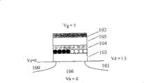
图1是一方框图,其说明了一现有技术的非易失存储单元的结构,其中一个非易失存储单元70包括有一N沟道金属氧化半导体场效晶体管(MOSFET)结构。非易失存储单元70包括有一个P型基底706,该P型基底706带有两个嵌入式N+结,其中一个为源极700,另一为漏极701。一个沟道707被形成在源极700与漏极701之间。在该沟道之上是一个第一绝缘层703,其通常为氧化硅层。在该第一绝缘层703的顶部是一个陷获层(trapping layer)704,其通常为氮化物层。陷获层704形成存储保持层,其在电子及空穴进入氮化物层时对其进行俘获。一个通常为氧化物层的第二绝缘层705被形成以覆盖该氮化硅层。氧化硅层705与一个被形成在该第二绝缘层705上的传导性栅极702相互电绝缘。这两个氧化硅层703极705用作绝缘介电层。FIG. 1 is a block diagram illustrating the structure of a prior art nonvolatile memory cell, wherein a
该现有技术结构可以提供一个二位单元,亦即非易失存储单元可以储存二位的数据。存储器是由沟道热电子注入来进行编程。通过将编程电压施加至栅极702与漏极701同时使源极700接地,电子可以被充分地加速以被注入至接近于漏极侧701的陷获层704中,以便增加接近于漏极侧701的沟道707中的能垒(energy barrier),在该漏极侧701中储存有数据的一个位。另外,电子可以被注入接近于源极侧702的陷获层704中,以便增加在沟道707中接近于源极侧700中的能垒,其中源极侧700储存有数据的另一个位。假如陷获层704包括有一适当的宽度,那么将电子储存在陷获层704中的两个区域可以被识别并被使用以储存数据的二个位。The prior art structure can provide a 2-bit cell, that is, the non-volatile memory cell can store 2-bit data. The memory is programmed by channel hot electron injection. By applying a programming voltage to the
关于现有技术的非易失存储单元的能垒,陷获层处于不带电状态(neutral state)。在没有电荷被储存于陷获层中之时,在沟道707中的能垒处于低状态。在对非易失存储单元进行编程过程中,电子被注入陷获层中,例如接近于漏极701处的陷获层中,以使在沟道707中接近于漏极701的能垒被提升。再者,当电子被注入接近于源极700的陷获层704中之时,在接近于源极700的沟道707中的能垒被提升。从而在沟道707中的能垒包括有被分配在能垒两侧的两个高区段。Regarding the energy barrier of the prior art nonvolatile memory cell, the trapping layer is in a neutral state. When no charge is stored in the trapping layer, the energy barrier in the
使用热电子注入的常规编程操作要求高操作电压并且消耗高功率。当非易失存储单元的尺寸被降低,并且沟道是相当小之时,高操作电压会诱导一种贯穿效应(punch-through effect),而造成高泄漏电流以及低编程效率。这些状况在现有技术的用作二位存储单元的非易失存储装置中变成一个显著的设计及实施缺点。此外,现有技术的结构需要一个特别局限的尺寸,这会妨碍在尺寸及成本降低上的工程成就。Conventional programming operations using hot electron injection require high operating voltages and consume high power. When the size of the nonvolatile memory cell is reduced and the channel is relatively small, the high operating voltage induces a punch-through effect, resulting in high leakage current and low programming efficiency. These conditions become a significant design and implementation disadvantage in prior art non-volatile memory devices used as two-bit memory cells. Furthermore, the prior art structures require a particularly limited size, which hinders engineering efforts in size and cost reduction.
因此,在本领域中所存在的需求是一种具有最佳二位单元结构的非易失存储装置,尤其是一种至少能够克服本领域中的非易失存储装置的前述缺点的非易失存储装置及其方法。特别是,在本领域中所存在的需求是一种具有针对俘获式介电层中所被俘获的电子电荷的扩大效应(amplified effects)、以及一最佳化降低尺寸的非易失存储装置。Therefore, there is a need in the art for a non-volatile storage device with an optimal two-bit cell structure, especially a non-volatile storage device capable of overcoming at least the aforementioned shortcomings of the non-volatile storage device in the art. Storage device and method thereof. In particular, what exists in the art is a nonvolatile memory device with amplified effects on electron charges trapped in a trapping dielectric layer and an optimized size reduction.
发明内容Contents of the invention
一种俘获式非易失存储单元,包括:一个P型半导体基底,该P型半导体基底包括有一个源极、一个与该源极分隔的漏极、以及一个被形成在该源极与该漏极之间的沟道;一个覆盖该沟道的隧道层,其中,该隧道层包括有用于电子与空穴的能垒;一个第一绝缘层,其覆盖住该隧道层,其中,该隧道层的能垒低于该第一绝缘层的能垒;一个非传导式电荷陷获层,其覆盖住该第一绝缘层;一个第二绝缘层,其覆盖住该非传导式电荷陷获层,该非传导式电荷陷获层包括有一个邻近于该漏极的第一电荷储存区和一个邻近于该源极的第二电荷储存区;及一个栅极,其覆盖住该第二绝缘层;在擦除状态时,该第一电荷存储区和第二电荷存储区接收并保持被注入该非传导式电荷层中的电子;在编程状态时,该第一电荷存储区或第二电荷存储区接收并保持被注入该非传导式电荷层中的空穴或拉出该非传导式电荷层中的电子。A trapping non-volatile memory unit, comprising: a P-type semiconductor substrate, the P-type semiconductor substrate includes a source, a drain separated from the source, and a drain formed between the source and the drain a channel between the poles; a tunnel layer covering the channel, wherein the tunnel layer includes energy barriers for electrons and holes; a first insulating layer covering the tunnel layer, wherein the tunnel layer an energy barrier lower than that of the first insulating layer; a non-conductive charge trapping layer covering the first insulating layer; a second insulating layer covering the non-conducting charge trapping layer, The non-conductive charge trapping layer includes a first charge storage region adjacent to the drain and a second charge storage region adjacent to the source; and a gate covering the second insulating layer; In the erasing state, the first charge storage area and the second charge storage area receive and hold the electrons injected into the non-conductive charge layer; in the programming state, the first charge storage area or the second charge storage area The holes injected into the non-conductive charge layer are received and held or the electrons are pulled out of the non-conductive charge layer.
在本发明的一较佳实施例中,该源极是一嵌入式N+结区域。In a preferred embodiment of the invention, the source is an embedded N+ junction region.
在本发明的一较佳实施例中,该漏极是一嵌入式N+结区域。In a preferred embodiment of the present invention, the drain is an embedded N+ junction region.
在本发明的一较佳实施例中,该栅极是由一导电材料所制成的。In a preferred embodiment of the present invention, the gate is made of a conductive material.
在本发明的一较佳实施例中,该第一及第二绝缘层是由氧化硅制成的。In a preferred embodiment of the present invention, the first and second insulating layers are made of silicon oxide.
在本发明的一较佳实施例中,该非传导式电荷陷获层是由氮化物制成的。In a preferred embodiment of the present invention, the non-conductive charge trapping layer is made of nitride.
在本发明的一较佳实施例中,该隧道层是从氧化钛及钡、锶、钽化合物所构成的一群中所选出之一个制成的。In a preferred embodiment of the present invention, the tunnel layer is made of one selected from the group consisting of titanium oxide and barium, strontium and tantalum compounds.
附图说明Description of drawings
本发明的较佳及其它实施例在下文中将参照附图(未依比例绘制)来加以更详细地说明,其中的附图为:Preferred and other embodiments of the invention are described in more detail hereinafter with reference to the accompanying drawings (not drawn to scale) in which:
图1说明了现有技术的非易失存储单元;Figure 1 illustrates a prior art non-volatile memory cell;
图2说明了根据本发明较佳实施例的非易失存储单元;Figure 2 illustrates a non-volatile memory cell according to a preferred embodiment of the present invention;
图3说明了根据本发明另一实施例而带有一隧道层的非易失存储单元;Figure 3 illustrates a non-volatile memory cell with a tunnel layer according to another embodiment of the present invention;
图4A以及图4B分别说明了针对根据本发明一实施例的非易失存储单元的源极位和漏极位来进行编程的示例性操作;FIG. 4A and FIG. 4B respectively illustrate an exemplary operation for programming a source bit and a drain bit of a nonvolatile memory cell according to an embodiment of the present invention;
图5A以及图5B分别说明了针对根据本发明另一实施例的非易失存储单元的源极位和漏极位来进行读取的示例性操作;FIG. 5A and FIG. 5B respectively illustrate an exemplary operation for reading a source bit and a drain bit of a nonvolatile memory cell according to another embodiment of the present invention;
图6A说明了在接近源极的一位处于低状态中、而接近漏极的位处于低状态和高状态中之时,用于读取接近源极的那个位的示例性能垒分布及电压分布;6A illustrates an example barrier distribution and voltage distribution for reading a bit near the source when the bit near the source is in the low state and the bit near the drain is in the low and high states ;
图6B说明了在接近源极的一位处于高状态中、而接近漏极的位处于低和高状态中之时,用于读取接近源极的那个位的示例性能垒分布及电压分布;6B illustrates an example barrier distribution and voltage distribution for reading a bit near the source when that bit is in the high state and the bits near the drain are in the low and high states;
图6C说明了在接近漏极的一位处于低状态中、而接近源极的位处于低和高状态中之时,用于读取接近漏极的那个位的示例性能垒分布及电压分布;6C illustrates an example barrier distribution and voltage distribution for reading a bit near the drain when the bit near the drain is in the low state and the bit near the source is in the low and high states;
图6D说明了在接近漏极的一位处于高状态中、而接近源极的位处于低和高状态中之时,用于读取接近漏极的那个位的示例性能垒分布及电压分布;FIG. 6D illustrates an example barrier distribution and voltage distribution for reading a bit near the drain when the bit near the drain is in the high state and the bits near the source are in the low and high states;
图7说明了根据本发明的示例性擦除操作,其中电子从半导体基底处被注入至陷获层之中;FIG. 7 illustrates an exemplary erase operation according to the present invention, wherein electrons are injected from a semiconductor substrate into a trapping layer;
图8说明了根据本发明的另一示例性擦除操作,其中电子从栅极处被注入至陷获层之中;FIG. 8 illustrates another exemplary erase operation according to the present invention, wherein electrons are injected from the gate into the trapping layer;
图9说明了根据本发明的快闪型存储单元的示例性擦除操作,其是通过以脉冲刺激该基底而从漏极处注入热电子;9 illustrates an exemplary erase operation of a flash memory cell according to the present invention by stimulating the substrate with pulses to inject hot electrons from the drain;
图10说明了根据本发明的快闪型存储单元的另一示例性擦除操作,其是通过以脉冲刺激该基底而从源极和漏极处注入热电子;10 illustrates another exemplary erase operation of a flash memory cell according to the present invention by stimulating the substrate with pulses to inject hot electrons from the source and drain;
图11说明了根据本发明的快闪型存储单元的再一示例性擦除操作,其是通过以脉冲刺激半导体基底而注入热电子;11 illustrates yet another exemplary erasing operation of a flash memory cell according to the present invention by stimulating the semiconductor substrate with pulses to inject hot electrons;
图12说明了根据本发明的非易失存储单元更进一步的示例性擦除操作,其是使用从N型阱处所发出的热电子来进行电子注入;以及12 illustrates a further exemplary erasing operation of a nonvolatile memory cell according to the present invention, which uses hot electrons emitted from an N-type well for electron injection; and
图13说明了根据本发明的非易失存储单元更进一步的示例性擦除操作,其是使用从N型注入器处所发出的热电子来进行电子注入。FIG. 13 illustrates a further exemplary erase operation of a non-volatile memory cell according to the present invention, which uses hot electrons emitted from an N-type injector for electron injection.
具体实施方式Detailed ways
本发明的细节将结合附图而在下文中进行描述。本领域的技术人员应当了解的是,以下描述内容包含本发明的示例性描述。在本发明的范围与精神中的修改以及变化因此为本发明的范畴所覆盖,而本发明的范畴是通过随附的权利要求及等价物所界定。Details of the invention will be described below with reference to the accompanying drawings. It should be appreciated by those skilled in the art that the following description contains exemplary descriptions of the present invention. Modifications and variations within the scope and spirit of the present invention are thus covered by the scope of the present invention as defined by the appended claims and their equivalents.
根据本发明一实施例的非易失存储单元10被说明于图2之中。非易失存储单元10一般包括有一个N沟道金属氧化半导体场效晶体管(MOSFET)结构。在非易失存储单元10中,一个P型基底106包括有两个嵌入式N+结,一个是源极100,而另一则是漏极101。一个沟道107被形成在该源极100与该漏极101之间。在该沟道107之上是一个第一绝缘层103,其通常为氧化硅层。在该第一绝缘层103的顶部是一个陷获层104,其通常为氮化物层。陷获层104形成了存储保持层,用于在电子与空穴被注入至氮化物层中之时对其进行俘获。一个通常为氧化硅层的第二绝缘层105被形成以覆盖住该氮化硅层。该氧化硅层105作用以对一个被形成在该第二绝缘层105上的传导性栅极102进行电绝缘。这两个氧化硅层103和105用作绝缘介电层。A
本发明的许多优点在于非易失存储器10被编程、被读取、以及被擦除的方式。在擦除状态之中,电子被储存在氮化物层之中,以使在沟道中的能阶(energy level)通常处于一高状态。在对非易失存储单元10进行编程之时,热空穴从源极100或漏极101处被注入陷获层104之中,以便改变能垒(energy barrier)。Many advantages of the present invention lie in the manner in which
在操作根据本发明的非易失存储单元之时,想要的是以高速将空穴或电子注入陷获层104之中。还想要的是在非易失存储单元并未操作之时得以将电子或空穴保持在陷获层中。根据本发明的一特殊实施例,针对一绝缘层(例如是第一绝缘层103)而言,电子的能垒是3.2eV,而空穴的能垒是4.9eV。这对于通过第一绝缘层103而被抽离以及被注入陷获层104的电子及空穴具有一等效效应。想要的是在非易失存储单元并未操作之时得以将电子或空穴稳定地保持在陷获层104中。相反地,当根据本发明的非易失存储单元在操作之时,电子及空穴能够被轻易地注入陷获层104之中。即,电子及空穴穿过一个具有较低能垒的绝缘层,以便加快非易失存储器的操作。When operating a nonvolatile memory cell according to the present invention, it is desirable to inject holes or electrons into the
图3说明了根据本发明一更进一步实施例而带有一隧道层的非易失存储单元。一个隧道层200被提供在该沟道107与该第一绝缘层103之间。揭示于图3中的结构大体上相似于在图2中所揭示的,除了一个隧道层200被附加在该沟道107与该第一绝缘层103间之外。隧道层200的材料被特别选定以提供较第一绝缘层103为低的电子及空穴的能垒,其中电子及空穴被轻易地注入陷获层中,从而在陷获层104中的电荷储存速度因此提升。由于第一绝缘层103维持在陷获层104旁边,在陷获层104中的电子或空穴亦被保持在其中。根据本发明的一特殊实施例,隧道层200的材料可以从氧化钛或BST(亦即钡、锶、以及钽的化合物)选出。FIG. 3 illustrates a non-volatile memory cell with a tunnel layer according to a further embodiment of the present invention. A tunnel layer 200 is provided between the channel 107 and the first insulating
在操作根据本发明和特殊实施例的非易失存储器时在擦除状态之中,电子被储存在陷获层104之中。在对根据本发明的非易失存储单元进行编程之时,热空穴被注入至陷获层104之中。Electrons are stored in trapping
快闪型存储单元100来自漏极位的操作被描述于本文中,并且在下文中进行更详细地描述。图4A说明了针对根据本发明的漏极位进行编程的示例性操作。为了程序化或写入本发明的非易失存储单元,一个电压差被形成在漏极101与栅极102之间,而源极100被接地。举例而言,一个-5V的电压被施加至该栅极102,并且一个5V的电压被施加至该漏极101。这些电压会产生一个沿着从漏极101至栅极102的垂直和横向电场。此电场会使空穴离开漏极101,并且加速朝向源极移动。空穴在其沿着沟道进行移动时会获得能量。当空穴获得充分能量之时,其能够跳过氧化硅层103的能垒而进入陷获层104之中,并且在陷获层104中被加以俘获。此状况发生的可能性在栅极邻近于漏极101的区域中是最大的,这是因为其接近于空穴(电子)获得最多能量的漏极101。这些加速移动的空穴(电子)被称为热空穴(电子)(hot holes)。一旦热空穴(电子)被注入氮化物层之中,其会被俘获并且保持被储存在其中。所俘获的空穴(电子)无法传播通过氮化物层,因为氮化物的低传导性以及横向电场所致。因此,所俘获的电荷维持在一个通常位于漏极附近的局部俘获区域中。再者,图4B说明了针对根据本发明的一源极位进行编程的示例性操作。源极位的编程大体上相似于漏极位的编程,除了被施加至源极100和漏极101的电压是可交换的以产生一不同效果之外。The operation of the
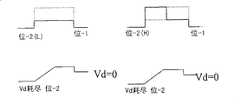
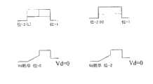
图5A说明了读取根据本发明的非易失存储单元的源极位的示例性操作。如果想要的是读取一个被储存在接近于源极100的陷获层中的位,则一个正电压被施加至栅极102以及漏极101,而源极100被接地。被施加至栅极102的正电压的下限是使充分反转产生于沟道107中的电压,藉此,已编程状态可以被感测到。被施加至漏极101的正电压会降低在储存在接近于漏极101的位上的能垒及电位,从而产生沟道电流并读取接近于源极100的位。图6A说明了在接近源极的一位处于低状态中、而接近漏极的位处于低状态和高状态中之时,用于读取接近源极的该位的能垒分布及电压分布。图6B说明了在接近源极的一位处于高状态中、而接近漏极的位处于低和高状态中之时,用于读取接近源极的该位的能垒分布及电压分布。FIG. 5A illustrates an exemplary operation of reading a source bit of a non-volatile memory cell according to the present invention. If it is desired to read a bit stored in the trapping layer close to the
当装置读取陷获层104中接近于漏极的位之时,如同在图5B中所说明的,一个正电压被施加至栅极102和源极100,而漏极101被接地。被施加至栅极102的正电压的下限是使充分反向产生于沟道107中的电压,藉此,已编程状态可以被感测到。被施加至源极100的正电压会降低在储存在接近于源极100的位上的能垒及电位,从而产生沟道电流。图6C说明了在接近漏极的一位处于低状态中、而接近源极的位处于低和高状态中之时,用于读取接近漏极的该位的示例性能垒分布及电压分布。图6D说明了在接近漏极的一位处于高状态中、而接近源极的位处于低和高状态中之时,用于读取接近漏极的该位的示例性能垒分布及电压分布。When the device reads the bit in
图7描述了根据本发明的弗勒诺德汉(Fowler-Nordheim;FN)注入法的示例性擦除操作,其中电子从半导体基底处被注入至陷获层之中。根据本发明的非易失存储单元通过一个用于基底注入的栅极-至-漏极/源极/基底的正偏压来进行弗勒诺德汉穿隧,而使用均匀电子注入来加以擦除。为了擦除挥发性存储单元,一个基底注入方法是想要的。电压被施加至源极100、漏极101、基底106、以及栅极102。举例而言,一个10V的电压被施加至栅极,而一个-5V的电压则被施加至漏极101、基底106、以及源极100。这些电压产生了一个沿着沟道区106至栅极102的垂直电场。这一电场会使电子离开沟道区,并接着穿过隧道向栅极运动。电子能够穿过隧道通过氧化硅层103的能垒(potential barrier)而被注入至陷获层104之中,而电子于陷获层104中被加以俘获。穿隧电子被注入氮化物层之中,而在氮化物层之中,电子被俘获并被保持储存于其中。FIG. 7 depicts an exemplary erase operation according to the Fowler-Nordheim (FN) injection method of the present invention, in which electrons are injected from the semiconductor substrate into the trapping layer. Non-volatile memory cells according to the present invention perform Fleur Nordheim tunneling with a positive gate-to-drain/source/substrate bias for substrate injection, while using uniform electron injection for erasure remove. For erasing volatile memory cells, a substrate injection method is desired. A voltage is applied to
再者,电压可以用于根据本发明的非易失存储单元的擦除操作,其使用用于基底注入的栅极-至-漏极/源极/基底的负偏压进行。图8说明了根据本发明的示例性擦除操作,其中电子使用FN(弗勒诺德汉)注入方法而从栅极处被注入至陷获层之中。电压因此被施加至源极100、漏极101、基底106、以及栅极102。举例而言,一个-10V的电压被施加至栅极,而5V的电压被施加至漏极101、基底106、以及源极100。这些电压产生了一个沿着栅极102至氮化物层104的长度的垂直电场。这一电场会使电子离开栅极102,并接着穿隧朝向氮化物层104。电子能够穿隧通过第二绝缘层105的能垒而被注入至陷获层104之中,而电子于陷获层104中被加以俘获。这些穿隧电子被注入陷获层之中,而在陷获层之中,电子被俘获并被保持储存于其中。Furthermore, voltages can be used for the erase operation of the non-volatile memory cell according to the present invention using negative gate-to-drain/source/substrate bias for substrate implantation. FIG. 8 illustrates an exemplary erase operation according to the present invention, where electrons are injected from the gate into the trapping layer using the FN (Fleur Nordheim) injection method. A voltage is thus applied to
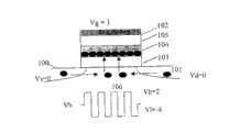
图9说明了根据本发明的快闪型存储单元的示例性擦除操作,其通过以脉冲刺激该基底而从漏极处注入热电子。存储单元经由热电子注入而通过脉冲刺激该基底而被加以擦除,其中,栅极102被正偏压,源极被浮接并且基底被接地,这是在一系列的双极脉冲被输入至漏极101之时。根据本发明的这一特殊实施例,栅极的电压是5V,其中脉冲的高压是4V,且其低压是-2V。当一负脉冲被输入至漏极101之时,在漏极中的电子因此从漏极101处流出而流向源极100。由于将一正脉冲施加至漏极101,介于漏极101与源极100之间的沟道被切断。当一电荷耗尽区(charge depletion region)被形成在基底106中,并且一电场沿着一个从漏极101至栅极102的路径被产生时,从漏极101处流出的电子被引导至栅极102,并接着被俘获在陷获层104中,以便完成擦除操作。FIG. 9 illustrates an exemplary erase operation of a flash memory cell according to the present invention by stimulating the substrate with pulses to inject hot electrons from the drain. The memory cell is erased by pulsing the substrate via hot electron injection, where the
在根据本发明的另一个实施例之中,序列脉冲(serial pulses)可以从源极100处输入,而漏极被浮接以达成大体上相同的结果。In another embodiment according to the present invention, serial pulses can be input from the
图10说明了根据本发明的快闪型存储单元的另一示例性擦除操作,其通过以脉冲刺激该基底而从源极和漏极处注入热电子。根据本发明的这一特殊实施例,栅极102被正偏压,并且基底被接地。一系列的双极脉冲被同步地输入至漏极101和源极100。当负脉冲被施加至源极100和漏极101之时,电子会离开源极100和漏极101,并接着加速朝向沟道107运动。当正脉冲被施加至源极100和漏极101之时,一个电荷耗尽区被形成在基底106之中,并且一电场沿着一个从沟道107至栅极102的路径被产生。垂直电场将电子抽离源极100和漏极101处,用以通过第一氧化硅层103而到达陷获层104。在以电子对陷获层进行充填一段时间的后,陷获层104充满了电子,以便擦除氮化物层中的原始状态。FIG. 10 illustrates another exemplary erase operation of a flash memory cell according to the present invention by stimulating the substrate with pulses to inject hot electrons from the source and drain. According to this particular embodiment of the invention, the
再者,脉冲可以被直接地施加至基底106,用以将电子抽离打入至陷获层。图11说明了根据本发明的快闪型存储单元的再一示例性擦除操作,其通过以脉冲刺激半导体基底而注入热电子。电子被抽离基底层106,并接着流动通过第一绝缘层103而到达至陷获层104。一个正电压(例如是3V)被施加至栅极102,而源极100和漏极101被接地。具有例如是2V的高状态以及例如是-4V的低状态的一系列脉冲被施加至基底106。在一正电压被施加之时,电子会离开源极100和漏极101。在一负电压被施加之时,离开源极100和漏极101的电子被抽离向上至陷获层104。在以电子对陷获层进行充填一段时间的后,陷获层104充满了电子,以便擦除氮化物层中的原始状态。Furthermore, pulses can be applied directly to the
图12说明了根据本发明的非易失存储单元更进一步的示例性擦除操作,其使用从N型阱处所发出的热电子来进行电子注入。根据本发明的非易失存储单元通过热电子注入来加以擦除,其中一个N型阱被提供环绕着非易失存储单元的基底。经由一个栅极-至-漏极/源极的正偏压以及一个P型阱-至-N型阱的正偏压,电子从N型阱发出、被注入至P型阱中、并且被俘获于存储单元之中,其中基底106用作为根据本发明此一特殊实施例的P型阱。一个N型阱109被形成以包围住基底106。一个P+区域108被形成在P型阱中,根据这一实施例,P+区域108位于但不限于位于N+漏极区域101的右侧。P+区域108被金属化,以用作一个将被连接至一外部部件的接点。更进一步包围住P型阱的N型阱109包括有一个N+区域110。N+区域110位于但不限于位于P+区域108的一侧。N+区域被金属化,以用作一个将被连接至一外部部件的接点。一个电压被提供在栅极102与N型阱109之间,以便将电子抽离N型阱而到达半导体基底106,并接着流动至陷获层104。如同在图12中所说明的相当大尺寸的这一N型阱有利地提供了相当大量的电子,以通过使用一相当小的电压而被注入至陷获层中。FIG. 12 illustrates a further exemplary erase operation of a non-volatile memory cell according to the present invention, which uses hot electrons emitted from the N-type well for electron injection. The nonvolatile memory cell according to the present invention is erased by hot electron injection, wherein an N-type well is provided surrounding the substrate of the nonvolatile memory cell. Electrons are emitted from the N-well, injected into the P-well, and trapped via a gate-to-drain/source positive bias and a P-well-to-N-well positive bias In the memory cell, the
应当了解的是,在本文中以及上文中连同图12所描述的特殊电压值仅包含用于执行根据本发明的非易失存储的擦除操作的一组可用条件。It should be appreciated that the particular voltage values described herein and above in connection with FIG. 12 only encompass a set of available conditions for performing an erase operation of the non-volatile storage according to the present invention.
图13说明了根据本发明的非易失存储单元的另一个示例性擦除操作,其使用从N型注入器处所发出的热电子来进行电子注入。根据本发明的非易失存储单元通过热电子注入来加以擦除,其中一个N+注入器被提供在非易失存储单元的基底之中。经由一个栅极-至-漏极/源极的正偏压以及一个P型阱-至-N+注入器的正偏压,电子从N+注入器发出,并接着被注入至P型阱中,而这些电子被俘获于存储单元之中,其中基底106用作为根据本发明这一特殊实施例的P型阱。一个N+注入器111被形成在P型阱中,其用以提供电子至P型阱,并且这些电子然后被注入至陷获层104中。一个P+区域108被形成在P型阱中。P+区域108被金属化,以用作一个将被连接至一外部部件的接点。根据本发明的这一实施例,N+注入器111以及P+区域108位于但不限于位于N+漏极区域101的右侧。一个电压被提供在栅极102与N+注入器111之间,以便将电子抽离N+注入器而进入P型阱,然后流动至陷获层104。如同在图12中所说明的相当大尺寸的这一N型阱有利地提供了相当大量的电子,以通过使用一相当小的电压而被注入至陷获层中。FIG. 13 illustrates another exemplary erasing operation of a nonvolatile memory cell according to the present invention, which uses hot electrons emitted from an N-type injector for electron injection. The nonvolatile memory cell according to the present invention is erased by hot electron injection, wherein an N+ injector is provided in the substrate of the nonvolatile memory cell. Through a gate-to-drain/source positive bias and a P-well-to-N+ injector positive bias, electrons are emitted from the N+ injector and then injected into the P-well, while These electrons are trapped in the memory cell, where
为了对根据本发明的非易失存储器进行编程,沟道被关闭。电流将不会从漏极101流动至源极100,或者沿着相反路径而流动。因此,本发明有利地防止了穿通效应的发生,穿通效应会造成大泄漏电流、高能量消耗、以及低编程效率,并且在存储单元中的二位可以被成功地识别。针对擦除操作而言,电子被储存在陷获层中,而在沟道中的能垒被提升。在沟道中的能垒级被均匀地分布在覆盖非易失存储单元中的两个位(一个位1以及一个位2)的区域之中。当位1被编程之时,在位1的一侧的能垒通过消耗被俘获的电子或热电子注入、补偿及重新组合陷获层中的载体而被降低。当位2被编程之时,在位2的一侧的能垒通过消耗被俘获的电子或热电子注入、补偿及重新组合陷获层中的载体而被降低。当位1及位2被编程之时,位1及位2二者的能垒被降低。由于来自栅极的电压将会切断沟道,因此将不会有电流贯穿该沟道。电流路径仅被形成于漏极与陷获层之间,或者介于源极与陷获层之间。当陷获层中的位1及位2是非常接近(紧邻彼此)之时,有利的是为了识别该二位而不会有分辨率降低。In order to program a non-volatile memory according to the invention, the channel is turned off. Current will not flow from
在以上实施例之中,用于对陷获层进行编程的方法是通过将空穴注入该层之中。当空穴被注入至该陷获层之时,其具有降低在该陷获层中的净电荷的效果。使电子离开陷获层亦达成实质上相同的结果。因此,使电子离开陷获层以达成写入非易失存储单元的目的的方法亦落于本发明的范畴之内。In the above embodiments, the method used to program the trapping layer is by injecting holes into this layer. When holes are injected into the trapping layer, it has the effect of reducing the net charge in the trapping layer. Letting the electrons leave the trapping layer also achieves essentially the same result. Therefore, the method of making electrons leave the trapping layer to achieve the purpose of writing the non-volatile memory cells also falls within the scope of the present invention.
虽然本发明一直参照较佳实施例来加以描述,将明白的是,本发明并不受限于其详细描述内容。替换及修改已于先前描述中所暗示,并且其它替换及修改将为本领域的技术人员所思及。特别是,根据本发明的方法的工艺步骤,将包括具有实质上相同于本发明的方法的工艺步骤、以达成实质上相同结果的方法。因此,所有这些替换及修改都会落在本发明于随附权利要求及其等价物所界定的范畴之中。While the present invention has been described with reference to preferred embodiments, it will be understood that the invention is not limited to the detailed description thereof. Alternatives and modifications have been suggested in the foregoing description, and others will occur to those skilled in the art. In particular, the process steps of the method according to the present invention shall include methods having substantially the same process steps as the method of the present invention to achieve substantially the same results. Accordingly, all such alternatives and modifications are intended to fall within the scope of the invention as defined in the appended claims and their equivalents.
Claims (7)
Translated fromChineseApplications Claiming Priority (2)
| Application Number | Priority Date | Filing Date | Title |
|---|---|---|---|
| US10/113,356US6690601B2 (en) | 2002-03-29 | 2002-03-29 | Nonvolatile semiconductor memory cell with electron-trapping erase state and methods for operating the same |
| US10/113,356 | 2002-03-29 |
Related Parent Applications (1)
| Application Number | Title | Priority Date | Filing Date |
|---|---|---|---|
| CNB031088163ADivisionCN100524767C (en) | 2002-03-29 | 2003-03-28 | Trapping nonvolatile memory cell and method for programming data using the same |
Publications (2)
| Publication Number | Publication Date |
|---|---|
| CN101582428A CN101582428A (en) | 2009-11-18 |
| CN101582428Btrue CN101582428B (en) | 2012-05-23 |
Family
ID=28453578
Family Applications (2)
| Application Number | Title | Priority Date | Filing Date |
|---|---|---|---|
| CN2009101297207AExpired - LifetimeCN101582428B (en) | 2002-03-29 | 2003-03-28 | A non-volatile semiconductor memory unit with electron trapping erased state and its operation method |
| CNB031088163AExpired - LifetimeCN100524767C (en) | 2002-03-29 | 2003-03-28 | Trapping nonvolatile memory cell and method for programming data using the same |
Family Applications After (1)
| Application Number | Title | Priority Date | Filing Date |
|---|---|---|---|
| CNB031088163AExpired - LifetimeCN100524767C (en) | 2002-03-29 | 2003-03-28 | Trapping nonvolatile memory cell and method for programming data using the same |
Country Status (2)
| Country | Link |
|---|---|
| US (1) | US6690601B2 (en) |
| CN (2) | CN101582428B (en) |
Families Citing this family (88)
| Publication number | Priority date | Publication date | Assignee | Title |
|---|---|---|---|---|
| JP2002184873A (en)* | 2000-10-03 | 2002-06-28 | Sony Corp | Nonvolatile semiconductor memory device and method of manufacturing the same |
| US7031196B2 (en)* | 2002-03-29 | 2006-04-18 | Macronix International Co., Ltd. | Nonvolatile semiconductor memory and operating method of the memory |
| US7057938B2 (en)* | 2002-03-29 | 2006-06-06 | Macronix International Co., Ltd. | Nonvolatile memory cell and operating method |
| US6894925B1 (en)* | 2003-01-14 | 2005-05-17 | Advanced Micro Devices, Inc. | Flash memory cell programming method and system |
| US6914819B2 (en)* | 2003-09-04 | 2005-07-05 | Macronix International Co., Ltd. | Non-volatile flash memory |
| US7049651B2 (en)* | 2003-11-17 | 2006-05-23 | Infineon Technologies Ag | Charge-trapping memory device including high permittivity strips |
| US6894932B1 (en)* | 2003-11-18 | 2005-05-17 | Advanced Micro Devices, Inc. | Dual cell memory device having a top dielectric stack |
| US7151692B2 (en)* | 2004-01-27 | 2006-12-19 | Macronix International Co., Ltd. | Operation scheme for programming charge trapping non-volatile memory |
| US7041545B2 (en)* | 2004-03-08 | 2006-05-09 | Infineon Technologies Ag | Method for producing semiconductor memory devices and integrated memory device |
| US7158411B2 (en)* | 2004-04-01 | 2007-01-02 | Macronix International Co., Ltd. | Integrated code and data flash memory |
| CN100463138C (en)* | 2004-04-26 | 2009-02-18 | 旺宏电子股份有限公司 | Charge balance operation method for charge trapping nonvolatile memory |
| US7075828B2 (en)* | 2004-04-26 | 2006-07-11 | Macronix International Co., Intl. | Operation scheme with charge balancing erase for charge trapping non-volatile memory |
| US7209390B2 (en)* | 2004-04-26 | 2007-04-24 | Macronix International Co., Ltd. | Operation scheme for spectrum shift in charge trapping non-volatile memory |
| US7133313B2 (en)* | 2004-04-26 | 2006-11-07 | Macronix International Co., Ltd. | Operation scheme with charge balancing for charge trapping non-volatile memory |
| US7164603B2 (en)* | 2004-04-26 | 2007-01-16 | Yen-Hao Shih | Operation scheme with high work function gate and charge balancing for charge trapping non-volatile memory |
| US7187590B2 (en)* | 2004-04-26 | 2007-03-06 | Macronix International Co., Ltd. | Method and system for self-convergent erase in charge trapping memory cells |
| JP2005317117A (en)* | 2004-04-28 | 2005-11-10 | Sony Corp | Operation method for nonvolatile semiconductor memory device, and nonvolatile semiconductor memory device |
| US7190614B2 (en)* | 2004-06-17 | 2007-03-13 | Macronix International Co., Ltd. | Operation scheme for programming charge trapping non-volatile memory |
| US7139200B2 (en)* | 2004-06-23 | 2006-11-21 | Macronix International Co., Ltd. | Method of identifying logical information in a programming and erasing cell by on-side reading scheme |
| US7274601B2 (en)* | 2004-09-27 | 2007-09-25 | Macronix International Co., Ltd. | Programming and erasing method for charge-trapping memory devices |
| US7209386B2 (en)* | 2004-07-06 | 2007-04-24 | Macronix International Co., Ltd. | Charge trapping non-volatile memory and method for gate-by-gate erase for same |
| US7120059B2 (en)* | 2004-07-06 | 2006-10-10 | Macronix International Co., Ltd. | Memory array including multiple-gate charge trapping non-volatile cells |
| CN1719598A (en)* | 2004-07-06 | 2006-01-11 | 旺宏电子股份有限公司 | Manufacturing method of multiple gate charge trapping non-volatile memory |
| US7387932B2 (en)* | 2004-07-06 | 2008-06-17 | Macronix International Co., Ltd. | Method for manufacturing a multiple-gate charge trapping non-volatile memory |
| US7106625B2 (en)* | 2004-07-06 | 2006-09-12 | Macronix International Co, Td | Charge trapping non-volatile memory with two trapping locations per gate, and method for operating same |
| US20060007732A1 (en)* | 2004-07-06 | 2006-01-12 | Macronix International Co., Ltd. | Charge trapping non-volatile memory and method for operating same |
| US7170785B2 (en)* | 2004-09-09 | 2007-01-30 | Macronix International Co., Ltd. | Method and apparatus for operating a string of charge trapping memory cells |
| CN100411149C (en)* | 2004-09-09 | 2008-08-13 | 旺宏电子股份有限公司 | Operation device and operation method of serially connected charge trapping memory cells |
| US7327611B2 (en)* | 2004-09-09 | 2008-02-05 | Macronix International Co., Ltd. | Method and apparatus for operating charge trapping nonvolatile memory |
| US7327607B2 (en)* | 2004-09-09 | 2008-02-05 | Macronix International Co., Ltd. | Method and apparatus for operating nonvolatile memory cells in a series arrangement |
| US7307888B2 (en)* | 2004-09-09 | 2007-12-11 | Macronix International Co., Ltd. | Method and apparatus for operating nonvolatile memory in a parallel arrangement |
| US7324376B2 (en)* | 2004-09-09 | 2008-01-29 | Macronix International Co., Ltd. | Method and apparatus for operating nonvolatile memory cells in a series arrangement |
| US7345920B2 (en) | 2004-09-09 | 2008-03-18 | Macronix International Co., Ltd. | Method and apparatus for sensing in charge trapping non-volatile memory |
| US7133317B2 (en)* | 2004-11-19 | 2006-11-07 | Macronix International Co., Ltd. | Method and apparatus for programming nonvolatile memory |
| US20060113586A1 (en)* | 2004-11-29 | 2006-06-01 | Macronix International Co., Ltd. | Charge trapping dielectric structure for non-volatile memory |
| US7272043B2 (en)* | 2004-12-27 | 2007-09-18 | Macronix International Co., Ltd. | Operation methods for a non-volatile memory cell in an array |
| US7130215B2 (en)* | 2004-12-28 | 2006-10-31 | Macronix International Co., Ltd. | Method and apparatus for operating a non-volatile memory device |
| US7072220B1 (en)* | 2004-12-28 | 2006-07-04 | Macronix International Co., Ltd. | Method and apparatus for operating a non-volatile memory array |
| US7072219B1 (en)* | 2004-12-28 | 2006-07-04 | Macronix International Co., Ltd. | Method and apparatus for operating a non-volatile memory array |
| KR100696766B1 (en)* | 2004-12-29 | 2007-03-19 | 주식회사 하이닉스반도체 | Charge Trap Insulator Memory Device |
| US7315474B2 (en) | 2005-01-03 | 2008-01-01 | Macronix International Co., Ltd | Non-volatile memory cells, memory arrays including the same and methods of operating cells and arrays |
| US8482052B2 (en) | 2005-01-03 | 2013-07-09 | Macronix International Co., Ltd. | Silicon on insulator and thin film transistor bandgap engineered split gate memory |
| US7473589B2 (en) | 2005-12-09 | 2009-01-06 | Macronix International Co., Ltd. | Stacked thin film transistor, non-volatile memory devices and methods for fabricating the same |
| US7186607B2 (en)* | 2005-02-18 | 2007-03-06 | Infineon Technologies Ag | Charge-trapping memory device and method for production |
| US7158420B2 (en) | 2005-04-29 | 2007-01-02 | Macronix International Co., Ltd. | Inversion bit line, charge trapping non-volatile memory and method of operating same |
| US7272040B2 (en)* | 2005-04-29 | 2007-09-18 | Infineon Technologies Ag | Multi-bit virtual-ground NAND memory device |
| DE102005025167B3 (en)* | 2005-06-01 | 2006-07-13 | Infineon Technologies Ag | Multi-bit virtual ground NAND-memory unit, has memory cells of two adjacent groups of rows connected in common |
| US7763927B2 (en) | 2005-12-15 | 2010-07-27 | Macronix International Co., Ltd. | Non-volatile memory device having a nitride-oxide dielectric layer |
| US7414888B2 (en)* | 2005-09-22 | 2008-08-19 | Macronix International Co., Ltd. | Program method and circuit of non-volatile memory |
| US7388252B2 (en)* | 2005-09-23 | 2008-06-17 | Macronix International Co., Ltd. | Two-bits per cell not-and-gate (NAND) nitride trap memory |
| US7881123B2 (en)* | 2005-09-23 | 2011-02-01 | Macronix International Co., Ltd. | Multi-operation mode nonvolatile memory |
| US7829586B2 (en)* | 2005-09-30 | 2010-11-09 | Banyu Pharmaceutical Co., Ltd. | Aryl-substituted nitrogen-containing heterocyclic compounds |
| US7321145B2 (en)* | 2005-10-13 | 2008-01-22 | Macronix International Co., Ltd. | Method and apparatus for operating nonvolatile memory cells with modified band structure |
| US7242622B2 (en)* | 2005-12-06 | 2007-07-10 | Macronix International Co., Ltd. | Methods to resolve hard-to-erase condition in charge trapping non-volatile memory |
| US7272038B2 (en)* | 2005-12-09 | 2007-09-18 | Macronix International Co., Ltd. | Method for operating gated diode nonvolatile memory cell |
| US7283389B2 (en)* | 2005-12-09 | 2007-10-16 | Macronix International Co., Ltd. | Gated diode nonvolatile memory cell array |
| US7269062B2 (en)* | 2005-12-09 | 2007-09-11 | Macronix International Co., Ltd. | Gated diode nonvolatile memory cell |
| US7491599B2 (en)* | 2005-12-09 | 2009-02-17 | Macronix International Co., Ltd. | Gated diode nonvolatile memory process |
| US7888707B2 (en)* | 2005-12-09 | 2011-02-15 | Macronix International Co., Ltd. | Gated diode nonvolatile memory process |
| US20070140019A1 (en)* | 2005-12-21 | 2007-06-21 | Macronix International Co., Ltd. | Method and apparatus for operating a string of charge trapping memory cells |
| TWI305917B (en)* | 2006-01-05 | 2009-02-01 | Macronix Int Co Ltd | Method and apparatus operating a string of charge trapping memory cells |
| US7292466B2 (en)* | 2006-01-03 | 2007-11-06 | Infineon Technologies Ag | Integrated circuit having a resistive memory |
| US7907450B2 (en) | 2006-05-08 | 2011-03-15 | Macronix International Co., Ltd. | Methods and apparatus for implementing bit-by-bit erase of a flash memory device |
| CN101449335A (en)* | 2006-05-19 | 2009-06-03 | Nxp股份有限公司 | Sonos memory device and method of operating a sonos memory device |
| US8772858B2 (en) | 2006-10-11 | 2014-07-08 | Macronix International Co., Ltd. | Vertical channel memory and manufacturing method thereof and operating method using the same |
| US7811890B2 (en) | 2006-10-11 | 2010-10-12 | Macronix International Co., Ltd. | Vertical channel transistor structure and manufacturing method thereof |
| US7492638B2 (en)* | 2006-11-20 | 2009-02-17 | Macronix International Co., Ltd. | Gated diode nonvolatile memory operation |
| US7723757B2 (en)* | 2006-11-20 | 2010-05-25 | Macronix International Co., Ltd. | Vertical nonvolatile memory cell, array, and operation |
| US7768825B2 (en)* | 2006-11-20 | 2010-08-03 | Macronix International Co., Ltd. | Gated diode nonvolatile memory structure with diffusion barrier structure |
| US7419868B2 (en)* | 2006-11-20 | 2008-09-02 | Macronix International Co., Ltd. | Gated diode nonvolatile memory process |
| US7561470B2 (en)* | 2006-12-21 | 2009-07-14 | Macronix International Co., Ltd. | Double-side-bias methods of programming and erasing a virtual ground array memory |
| US7554851B2 (en)* | 2007-01-05 | 2009-06-30 | Macronix International Co., Ltd. | Reset method of non-volatile memory |
| CN100555640C (en)* | 2007-01-16 | 2009-10-28 | 旺宏电子股份有限公司 | reset method of non-volatile memory |
| US8223540B2 (en)* | 2007-02-02 | 2012-07-17 | Macronix International Co., Ltd. | Method and apparatus for double-sided biasing of nonvolatile memory |
| US7737488B2 (en) | 2007-08-09 | 2010-06-15 | Macronix International Co., Ltd. | Blocking dielectric engineered charge trapping memory cell with high speed erase |
| US7916551B2 (en)* | 2007-11-06 | 2011-03-29 | Macronix International Co., Ltd. | Method of programming cell in memory and memory apparatus utilizing the method |
| US7974127B2 (en) | 2007-11-06 | 2011-07-05 | Macronix International Co., Ltd. | Operation methods for memory cell and array for reducing punch through leakage |
| WO2009122582A1 (en)* | 2008-04-03 | 2009-10-08 | 株式会社 東芝 | Nonvolatile recording device and process for producing the same |
| KR101466697B1 (en)* | 2008-07-10 | 2014-12-01 | 삼성전자주식회사 | How to program memory devices and memory data |
| US7995384B2 (en)* | 2008-08-15 | 2011-08-09 | Macronix International Co., Ltd. | Electrically isolated gated diode nonvolatile memory |
| US7986564B2 (en)* | 2008-09-19 | 2011-07-26 | Macronix International Co., Ltd. | High second bit operation window method for virtual ground array with two-bit memory cells |
| US8143665B2 (en)* | 2009-01-13 | 2012-03-27 | Macronix International Co., Ltd. | Memory array and method for manufacturing and operating the same |
| US9240405B2 (en) | 2011-04-19 | 2016-01-19 | Macronix International Co., Ltd. | Memory with off-chip controller |
| JP2013196731A (en)* | 2012-03-21 | 2013-09-30 | Toshiba Corp | Nonvolatile semiconductor memory device |
| US8891299B2 (en)* | 2012-08-09 | 2014-11-18 | Taiwan Semiconductor Manufacturing Company, Ltd. | MOSFET having memory characteristics |
| US9312017B2 (en)* | 2014-01-15 | 2016-04-12 | Apple Inc. | Storage in charge-trap memory structures using additional electrically-charged regions |
| US10290352B2 (en)* | 2015-02-27 | 2019-05-14 | Qualcomm Incorporated | System, apparatus, and method of programming a one-time programmable memory circuit having dual programming regions |
| US10043584B2 (en) | 2016-10-28 | 2018-08-07 | International Business Machines Corporation | Three terminal fuse structure created by oxygen vacancy traps in hafnium-based oxides |
Citations (1)
| Publication number | Priority date | Publication date | Assignee | Title |
|---|---|---|---|---|
| US5774400A (en)* | 1995-12-26 | 1998-06-30 | Nvx Corporation | Structure and method to prevent over erasure of nonvolatile memory transistors |
Family Cites Families (14)
| Publication number | Priority date | Publication date | Assignee | Title |
|---|---|---|---|---|
| US5168334A (en) | 1987-07-31 | 1992-12-01 | Texas Instruments, Incorporated | Non-volatile semiconductor memory |
| US6330190B1 (en)* | 1996-05-30 | 2001-12-11 | Hyundai Electronics America | Semiconductor structure for flash memory enabling low operating potentials |
| US5768192A (en) | 1996-07-23 | 1998-06-16 | Saifun Semiconductors, Ltd. | Non-volatile semiconductor memory cell utilizing asymmetrical charge trapping |
| US6768165B1 (en)* | 1997-08-01 | 2004-07-27 | Saifun Semiconductors Ltd. | Two bit non-volatile electrically erasable and programmable semiconductor memory cell utilizing asymmetrical charge trapping |
| JP3999900B2 (en)* | 1998-09-10 | 2007-10-31 | 株式会社東芝 | Nonvolatile semiconductor memory |
| US6282123B1 (en)* | 1998-12-21 | 2001-08-28 | Lattice Semiconductor Corporation | Method of fabricating, programming, and erasing a dual pocket two sided program/erase non-volatile memory cell |
| DE19903598A1 (en)* | 1999-01-29 | 2000-08-10 | Siemens Ag | Multi-dielectric semiconductor device |
| US6272050B1 (en)* | 1999-05-28 | 2001-08-07 | Vlsi Technology, Inc. | Method and apparatus for providing an embedded flash-EEPROM technology |
| US6134150A (en)* | 1999-07-23 | 2000-10-17 | Aplus Flash Technology, Inc. | Erase condition for flash memory |
| JP3775963B2 (en)* | 2000-02-02 | 2006-05-17 | シャープ株式会社 | Erase method for nonvolatile semiconductor memory device |
| US6215702B1 (en)* | 2000-02-16 | 2001-04-10 | Advanced Micro Devices, Inc. | Method of maintaining constant erasing speeds for non-volatile memory cells |
| JP3751499B2 (en)* | 2000-03-23 | 2006-03-01 | 株式会社東芝 | Semiconductor device and manufacturing method thereof |
| US6487121B1 (en)* | 2000-08-25 | 2002-11-26 | Advanced Micro Devices, Inc. | Method of programming a non-volatile memory cell using a vertical electric field |
| US6487114B2 (en)* | 2001-02-28 | 2002-11-26 | Macronix International Co., Ltd. | Method of reading two-bit memories of NROM cell |
- 2002
- 2002-03-29USUS10/113,356patent/US6690601B2/ennot_activeExpired - Lifetime
- 2003
- 2003-03-28CNCN2009101297207Apatent/CN101582428B/ennot_activeExpired - Lifetime
- 2003-03-28CNCNB031088163Apatent/CN100524767C/ennot_activeExpired - Lifetime
Patent Citations (1)
| Publication number | Priority date | Publication date | Assignee | Title |
|---|---|---|---|---|
| US5774400A (en)* | 1995-12-26 | 1998-06-30 | Nvx Corporation | Structure and method to prevent over erasure of nonvolatile memory transistors |
Non-Patent Citations (2)
| Title |
|---|
| JP特开2001-57093A 2001.02.27 |
| JP特开平11-31394A 1999.02.02 |
Also Published As
| Publication number | Publication date |
|---|---|
| CN1449049A (en) | 2003-10-15 |
| CN101582428A (en) | 2009-11-18 |
| US20030185055A1 (en) | 2003-10-02 |
| US6690601B2 (en) | 2004-02-10 |
| CN100524767C (en) | 2009-08-05 |
Similar Documents
| Publication | Publication Date | Title |
|---|---|---|
| CN101582428B (en) | A non-volatile semiconductor memory unit with electron trapping erased state and its operation method | |
| US6614694B1 (en) | Erase scheme for non-volatile memory | |
| US6798699B2 (en) | Flash memory device and method of erasing | |
| US7149125B1 (en) | Location-specific NAND (LS NAND) memory technology and cells | |
| US6829175B2 (en) | Erasing method for non-volatile memory | |
| US6009017A (en) | Floating gate memory with substrate band-to-band tunneling induced hot electron injection | |
| US6930928B2 (en) | Method of over-erase prevention in a non-volatile memory device and related structure | |
| US7515479B2 (en) | Nonvolatile semiconductor storage device and method for writing therein | |
| US5790460A (en) | Method of erasing a flash EEPROM memory | |
| JPH04285795A (en) | Non-volatile memory that enhances carrier generation and its programming method | |
| TW476144B (en) | Non-volatile memory | |
| JP2993358B2 (en) | Operating method of nonvolatile semiconductor memory device | |
| CN100379028C (en) | Electronic circuit, system, non-volatile memory and operation method thereof | |
| KR100558004B1 (en) | Programming method of a nonvolatile memory device having a charge storage layer between a gate electrode and a semiconductor substrate | |
| JP4801897B2 (en) | Nonvolatile semiconductor memory and method of operating the memory | |
| US7209385B1 (en) | Array structure for assisted-charge memory devices | |
| CN1333407C (en) | Data Retention in Partially Captured Nonvolatile Memory | |
| US6906959B2 (en) | Method and system for erasing a nitride memory device | |
| JP2963882B2 (en) | Flash memory cell programming method | |
| JP5162075B2 (en) | Nonvolatile semiconductor memory and operation method thereof | |
| CN101325180B (en) | Apparatus and method for self-convergence when erasing non-volatile memory elements | |
| JPH0997884A (en) | Nonvolatile semiconductor memory device | |
| US7206227B1 (en) | Architecture for assisted-charge memory array | |
| EP1553635A1 (en) | Nonvolatile semiconductor memory and operating method of the memory | |
| US6424573B1 (en) | Floating gate field effect transistor and method of driving the same |
Legal Events
| Date | Code | Title | Description |
|---|---|---|---|
| C06 | Publication | ||
| PB01 | Publication | ||
| C10 | Entry into substantive examination | ||
| SE01 | Entry into force of request for substantive examination | ||
| C14 | Grant of patent or utility model | ||
| GR01 | Patent grant | ||
| CX01 | Expiry of patent term | ||
| CX01 | Expiry of patent term | Granted publication date:20120523 |