CN101578686A - Method for manufacturing micro-electromechanical device - Google Patents
Method for manufacturing micro-electromechanical deviceDownload PDFInfo
- Publication number
- CN101578686A CN101578686ACNA2006800226444ACN200680022644ACN101578686ACN 101578686 ACN101578686 ACN 101578686ACN A2006800226444 ACNA2006800226444 ACN A2006800226444ACN 200680022644 ACN200680022644 ACN 200680022644ACN 101578686 ACN101578686 ACN 101578686A
- Authority
- CN
- China
- Prior art keywords
- layer
- cavity
- top board
- substrate wafer
- connector
- Prior art date
- Legal status (The legal status is an assumption and is not a legal conclusion. Google has not performed a legal analysis and makes no representation as to the accuracy of the status listed.)
- Granted
Links
Images


Classifications
- H—ELECTRICITY
- H01—ELECTRIC ELEMENTS
- H01L—SEMICONDUCTOR DEVICES NOT COVERED BY CLASS H10
- H01L21/00—Processes or apparatus adapted for the manufacture or treatment of semiconductor or solid state devices or of parts thereof
- H01L21/70—Manufacture or treatment of devices consisting of a plurality of solid state components formed in or on a common substrate or of parts thereof; Manufacture of integrated circuit devices or of parts thereof
- H01L21/71—Manufacture of specific parts of devices defined in group H01L21/70
- H01L21/768—Applying interconnections to be used for carrying current between separate components within a device comprising conductors and dielectrics
- H01L21/76898—Applying interconnections to be used for carrying current between separate components within a device comprising conductors and dielectrics formed through a semiconductor substrate
- H—ELECTRICITY
- H01—ELECTRIC ELEMENTS
- H01L—SEMICONDUCTOR DEVICES NOT COVERED BY CLASS H10
- H01L23/00—Details of semiconductor or other solid state devices
- H01L23/48—Arrangements for conducting electric current to or from the solid state body in operation, e.g. leads, terminal arrangements ; Selection of materials therefor
- H01L23/481—Internal lead connections, e.g. via connections, feedthrough structures
- H—ELECTRICITY
- H01—ELECTRIC ELEMENTS
- H01L—SEMICONDUCTOR DEVICES NOT COVERED BY CLASS H10
- H01L2924/00—Indexing scheme for arrangements or methods for connecting or disconnecting semiconductor or solid-state bodies as covered by H01L24/00
- H01L2924/0001—Technical content checked by a classifier
- H01L2924/0002—Not covered by any one of groups H01L24/00, H01L24/00 and H01L2224/00
- H—ELECTRICITY
- H01—ELECTRIC ELEMENTS
- H01L—SEMICONDUCTOR DEVICES NOT COVERED BY CLASS H10
- H01L2924/00—Indexing scheme for arrangements or methods for connecting or disconnecting semiconductor or solid-state bodies as covered by H01L24/00
- H01L2924/30—Technical effects
- H01L2924/301—Electrical effects
- H01L2924/3011—Impedance
Landscapes
- Engineering & Computer Science (AREA)
- Physics & Mathematics (AREA)
- Condensed Matter Physics & Semiconductors (AREA)
- General Physics & Mathematics (AREA)
- Computer Hardware Design (AREA)
- Microelectronics & Electronic Packaging (AREA)
- Power Engineering (AREA)
- Manufacturing & Machinery (AREA)
- Internal Circuitry In Semiconductor Integrated Circuit Devices (AREA)
- Transducers For Ultrasonic Waves (AREA)
- Micromachines (AREA)
Abstract
Description
Translated fromChinese本申请要求以下美国临时申请的优先权:2005年5月18日提交的第60/682,619号;2005年6月17日提交的第60/692,038号;2005年8月3日提交的第60/705,606号;2006年4月4日提交的第60/744242号,这些专利申请的内容通过引用整体结合于此。This application claims priority to the following U.S. Provisional Applications: 60/682,619, filed May 18, 2005; 60/692,038, filed June 17, 2005; 60/692,038, filed August 3, 2005 705,606; 60/744,242, filed April 4, 2006, the contents of which are hereby incorporated by reference in their entirety.
本申请还通过引用结合了以下申请的全部内容:This application also incorporates by reference the entire contents of the following applications:
由共同的申请人在与本申请相同的日期提交的名为THROUGH-WAFERINTERCONNECTION(代理机构案号03004.01)的国际申请(PCT);International Application (PCT) entitled THROUGH-WAFERINTERCONNECTION (Attorney Docket No. 03004.01), filed by a common applicant on the same date as the present application;
由共同的申请人在与本申请相同的日期提交的名为MICRO-ELECTRO-MECHANICAL TRANSDUCERS(代理机构案号03004.03)的国际申请(PCT);International Application (PCT) entitled MICRO-ELECTRO-MECHANICAL TRANSDUCERS (Attorney Docket No. 03004.03), filed by a common applicant on the same date as the present application;
由共同的申请人在与本申请相同的日期提交的名为MICRO-ELECTRO-MECHANICAL TRANSDUCERS(代理机构案号03004.04)的国际申请(PCT)。International Application (PCT) entitled MICRO-ELECTRO-MECHANICAL TRANSDUCERS (Attorney Docket No. 03004.04), filed by common applicant on the same date as the present application.
技术领域technical field
本申请涉及微电子制造,尤其涉及诸如具有用于能量转换的可移动机械部件的微加工超声换能器(MUT)之类的微机电装置的制造方法。The present application relates to microelectronics fabrication, and more particularly to methods of fabricating microelectromechanical devices such as micromachined ultrasonic transducers (MUTs) with movable mechanical parts for energy conversion.
背景技术Background technique
微机电系统(MEMS)是通过微制造技术在共用衬底(一般是硅衬底)上的机械元件、传感器、执行器和电子装置的集成。MEMS希望将基于硅的微电子与微加工技术结合起来,使实现在一个芯片上的完整系统成为可能。利用发展良好且高效的半导体制造技术制造微传感器和微执行器的前景是关于MEMS的有力的主题。Micro-Electro-Mechanical Systems (MEMS) is the integration of mechanical elements, sensors, actuators, and electronics on a common substrate (usually a silicon substrate) through microfabrication techniques. MEMS hopes to combine silicon-based microelectronics with microfabrication technology to make it possible to realize a complete system on a chip. The prospect of making microsensors and microactuators using well-developed and efficient semiconductor fabrication techniques is a powerful theme with regard to MEMS.
MEMS装置一般具有集成在一起的两个主要组件。第一组件是利用通常的集成电路(IC)工艺(例如,CMOS、双极或BICOMS工艺)制造的电子器件,而第二组件是利用兼容的微加工工艺制造的微机械部件。微加工指的是利用选择性加手段(沉积、接合、注入等)和减手段(化学蚀刻、等离子体蚀刻、激光烧蚀、离子铣削)制造显微结构的制造工艺。当与图案化手段结合时,可用的加手段和减手段使微加工成为形成令人兴奋的新的微器件的强大的方法。MEMS devices generally have two main components integrated together. The first component is an electronic device fabricated using a common integrated circuit (IC) process (eg, CMOS, bipolar or BICOMS process), while the second component is a micromechanical component fabricated using a compatible micromachining process. Micromachining refers to manufacturing processes that utilize selective additive means (deposition, bonding, implantation, etc.) and subtractive means (chemical etching, plasma etching, laser ablation, ion milling) to create microstructures. When combined with patterning means, the available plus and minus means make microfabrication a powerful method for forming exciting new microdevices.
MEMS装置的一个例子是微加工超声换能器(MUT)。超声换能器执行一系列的能量转换以实现其换能器的功能。在其接收模式中,在放置了换能器的介质中传播的超声波的声能被转换成换能器中的可移动部件(通常是振动膜)的机械能。然后可移动部件的运动被转换成可检测的电磁(通常是电)信号。在其发射器模式中,发生反向的能量转换过程。One example of a MEMS device is a micromachined ultrasound transducer (MUT). Ultrasonic transducers perform a series of energy transformations to achieve their transducer functions. In its receive mode, the acoustic energy of ultrasonic waves propagating in the medium in which the transducer is placed is converted into mechanical energy of a movable part in the transducer (usually a diaphragm). The motion of the movable part is then converted into a detectable electromagnetic (usually electrical) signal. In its transmitter mode, the reverse energy conversion process takes place.
已经开发了用于发射和接收超声波的各种类型的超声换能器。超声换能器可在各种介质中工作,包括液体、固体和气体。这些换能器通常用于诊断和治疗的医学成像、生物化学成像、材料的非破坏性检测、声纳、通信、贴近式传感器、气流测量、现场过程监视、声学显微镜、水下传感和成像以及许多其它方面。除分立的超声换能器外,还开发了包含多个换能器的超声换能器阵列。例如,开发了用于成像应用的二维阵列超声换能器。Various types of ultrasonic transducers have been developed for transmitting and receiving ultrasonic waves. Ultrasonic transducers operate in a variety of media, including liquids, solids and gases. These transducers are commonly used in diagnostic and therapeutic medical imaging, biochemical imaging, non-destructive inspection of materials, sonar, communications, proximity sensors, airflow measurement, in-situ process monitoring, acoustic microscopy, underwater sensing and imaging and many others. In addition to discrete ultrasound transducers, ultrasound transducer arrays containing multiple transducers have also been developed. For example, two-dimensional arrays of ultrasound transducers have been developed for imaging applications.
与广泛使用的压电(PZT)超声换能器相比,MUT在装置制造方法、带宽和工作温度方面具有优势。例如,制造常规的PZT换能器阵列包括切割和连接各个的压电元件。该工艺充满了困难和高花费,更不用说由这些元件造成的对发射/接收电子装置的大的输入阻抗失配问题。在比较中,在制造MUT中使用的微加工技术更加胜任制造这种阵列。在性能方面,MUT证明了可与PZT换能器的动态性能相比较的动态性能。由于这些原因,MUT正在成为压电(PZT)超声换能器的引人注目的替换对象。Compared with widely used piezoelectric (PZT) ultrasound transducers, MUTs have advantages in terms of device fabrication method, bandwidth, and operating temperature. For example, fabricating a conventional PZT transducer array involves cutting and joining individual piezoelectric elements. The process is fraught with difficulty and expense, not to mention the large input impedance mismatch to the transmit/receive electronics caused by these components. In comparison, the microfabrication techniques used in the fabrication of MUTs are more adequate to fabricate such arrays. In terms of performance, the MUT demonstrates a dynamic performance comparable to that of the PZT transducer. For these reasons, MUTs are becoming an attractive replacement for piezoelectric (PZT) ultrasound transducers.
在几种类型的MUT中,广泛使用电容式微加工超声换能器(cMUT),它采用静电换能器。还采用利用压电换能器(pMUT)和磁换能器(mMUT)的其它MUT。Among several types of MUTs, capacitive micromachined ultrasonic transducers (cMUTs), which employ electrostatic transducers, are widely used. Other MUTs utilizing piezoelectric transducers (pMUTs) and magnetic transducers (mMUTs) are also employed.
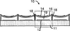
图1示出了具有多个单元的现有技术cMUT的基本结构的横截面图。示出了四个单元。cMUT构造在衬底10上,并具有平行板电容器,该平行板电容器由刚性底电极12和位于柔性膜16上或其中并用于在相邻介质中发射或接收声波的顶电极14组成。每一个单元中的柔性膜16由绝缘壁或柱18支承。实际上,cMUT由很多并联连接的单元形成。将DC偏压施加在电极12和14之间,以使膜16偏转到用于cMUT工作的最优位置,通常以使灵敏度和带宽最大化为目标。在发射期间,将AC信号施加到换能器。顶电极和底电极之间的交替的静电力激励膜16,以便将声能传递到cMUT周围的介质(未示出)中。在接收期间,发射过来的声波振动膜16,因此改变了两电极之间的电容。电子电路检测该电容变化。或者可利用压电换能器(pMUT)和磁换能器(mMUT)激励膜并检测膜的位移。Figure 1 shows a cross-sectional view of the basic structure of a prior art cMUT with multiple cells. Four cells are shown. The cMUT is constructed on a
已经开发了用于制造图1所示的cMUT的制造方法。在美国专利第6,632,178号和6,958,255号中公开了示例性方法。A fabrication method for fabricating the cMUT shown in Fig. 1 has been developed. Exemplary methods are disclosed in US Patent Nos. 6,632,178 and 6,958,255.
在现有技术的结构和方法的cMUT中存在缺点。这些缺点中的很多涉及这样的事实,即cMUT元件由很多单独的单元形成,并且cMUT膜在其边缘上夹紧或固定。以下列出了缺点的例子。There are disadvantages in cMUTs of prior art structures and methods. Many of these disadvantages relate to the fact that the cMUT element is formed from many individual cells and the cMUT membrane is clamped or fixed at its edges. Examples of disadvantages are listed below.
(1)由于夹紧边缘,膜的平均位移小。结果装置的发射和接收性能都差。(1) The average displacement of the membrane is small due to the clamped edges. As a result, the transmit and receive performance of the device is poor.
(2)由夹紧区域(例如边缘)和壁或柱占用的表面面积不活动,因此降低了装置的填充因数和总效率。(2) The surface area occupied by the clamping regions (eg, edges) and walls or columns is inactive, thus reducing the fill factor and overall efficiency of the device.
(3)锚固区域引入寄生电容,这降低了装置的灵敏度。(3) The anchoring region introduces parasitic capacitance, which reduces the sensitivity of the device.
(4)cMUT元件的表面内的锚固图案可导致超声波干涉,这限制了装置带宽。(4) Anchoring patterns within the surface of cMUT elements can lead to ultrasonic interference, which limits device bandwidth.
(5)膜的不一致的位移可扰乱超声波图案。例如,不一致的位移可影响从换能器表面发射的超声束图案并还导致通过换能器表面的声交叉耦合。(5) Inconsistent displacement of the membrane can disturb the ultrasound pattern. For example, inconsistent displacement can affect the ultrasound beam pattern emitted from the transducer surface and also cause acoustic cross-coupling through the transducer surface.
(6)由于工艺偏差同一cMUT元件中的各个单元的谐振频率可能互不相同。这导致工作期间同一cMUT元件中不同单元之间膜运动的相位差。结果,cMUT元件的平均位移的和将显著劣化。该问题劣化了装置的性能,尤其是在cMUT在高品质因数(Q-因数)条件下工作时,例如在空气中。(6) The resonant frequencies of the units in the same cMUT element may be different from each other due to process variation. This leads to a phase difference in membrane motion between different cells in the same cMUT element during operation. As a result, the sum of the average displacements of the cMUT elements will be significantly degraded. This problem degrades the performance of the device, especially when the cMUT operates under high quality factor (Q-factor) conditions, such as in air.
(7)声能可通过支承壁耦合到换能器衬底并导致诸如cMUT元件之间的声交叉耦合之类的不希望的效果。通过引入具有期望声音特性的材料降低穿过衬底的交叉耦合的工作需要占用元件之间额外的空间。(7) Acoustic energy can couple to the transducer substrate through the support walls and cause undesired effects such as acoustic cross-coupling between cMUT elements. Efforts to reduce cross-coupling across the substrate by introducing materials with desired acoustic properties require additional space between components.
以上的问题也存在于现有技术的pMUT和mMUT中因为它们具有与如图1所示cMUT相似的结构。The above problems also exist in the prior art pMUT and mMUT because they have a similar structure to the cMUT shown in FIG. 1 .
在美国专利第7,030,536号中公开了用于制造具有构造在衬底上的柔性的(compliant)支承结构以支承膜的cMUT装置的另一种制造方法。与图1中所示的常规的cMUT结构相比,美国专利第7,030,536号中公开的结构利用柔性支承结构来代替常规的绝缘壁18,用于固定膜16的周边端。因为相对复杂的柔性支承结构代替了图1中的简单且窄的绝缘壁18以成为支承周边,所以制造由根据该设计的这些周边支承结构占据的不活动的区域存在更高的挑战。该专利还建议在柔性支承结构上制造补充电极以减小由柔性支承结构占据的不活动的面积。然而,没有迹象表明这一设计可解决以上发现的问题,甚至根本不管它是否起作用。Another fabrication method for fabricating a cMUT device with a compliant support structure built on a substrate to support the membrane is disclosed in US Patent No. 7,030,536. Compared with the conventional cMUT structure shown in FIG. 1 , the structure disclosed in US Pat. No. 7,030,536 utilizes a flexible supporting structure instead of the conventional insulating
一般而言,上述的MUT属于具有用于能量转换的可移动机械部件的一种类型的MEMS装置。这一可移动部件的制造及其与MEMS制造的其它方面的集成提出了挑战。由于这些诸如MUT之类的MEMS装置的重要性,期望在性能、功能性和可制造性方面改进技术。In general, the MUTs described above belong to a type of MEMS device that has movable mechanical parts for energy conversion. The fabrication of this movable part and its integration with other aspects of MEMS fabrication present challenges. Due to the importance of these MEMS devices such as MUTs, it is desirable to improve the technology in terms of performance, functionality and manufacturability.
发明内容Contents of the invention
本申请公开了一种用于各种应用的具有可移动机械部件以转换能量的微机电装置的制造方法。该方法形成具有衬底晶片、中间弹性层和顶板层的多层结构。在衬底晶片的顶部或中间弹性层的底部形成空腔。在中间弹性层的顶部或顶板层的底部上形成连接器。将衬底晶片、中间弹性层和顶板以该顺序接合起来。在接合这些层之后,连接器从中间弹性层直立以在顶板层和中间弹性层之间限定换能空间。连接器在水平方向上离开空腔的侧壁足够的长度以限定锚固在侧壁处的悬臂。悬臂和空腔允许连接器的垂直位移,连接器以类似于活塞的运动移动顶部晶片,以改变换能空间。The present application discloses a method of fabricating a microelectromechanical device with movable mechanical parts to convert energy for various applications. The method forms a multilayer structure having a substrate wafer, a middle elastic layer, and a top plate layer. A cavity is formed at the top of the substrate wafer or at the bottom of the intermediate elastic layer. Connectors are formed on the top of the middle elastic layer or the bottom of the top sheet layer. The substrate wafer, the intermediate elastic layer and the top plate are bonded in this order. After joining the layers, connectors stand up from the middle elastic layer to define a transducing space between the top deck layer and the middle elastic layer. The connector is horizontally spaced from the sidewall of the cavity by a sufficient length to define a cantilever anchored at the sidewall. The cantilever and cavity allow vertical displacement of the connector, which moves the top wafer in a piston-like motion to change the transducing volume.
在一个实施例中,中间弹性层锚固在空腔的两个相对侧壁处以覆盖空腔。中间弹性层上的连接器位于空气上,并离开两个相对侧壁以形成可视为头对头双悬臂的桥。在更有效的构造中,由中间弹性层形成区域或平面弹簧(二维“悬臂”),而不是类似于梁的一位悬臂。In one embodiment, the intermediate elastic layer is anchored at two opposite side walls of the cavity to cover the cavity. The connectors on the middle elastic layer sit on air and away from the two opposing side walls to form a bridge that can be viewed as a head-to-head double cantilever. In a more efficient configuration, a region or planar spring (a two-dimensional "cantilever") is formed by an intermediate elastic layer, rather than a one-dimensional cantilever like a beam.
该方法利用晶片接合技术、表面微加工牺牲层技术来实现与半导体制造工艺的多功能且高水平的集成。可利用该方法制造具有用于转换能量的可移动机械部件的宽范围的微机电装置。这些装置包括但不限于诸如电容式微加工超声换能器(cMUT)、压电微加工超声换能器(pMUT)和磁微加工超声换能器(mMUT)之类的微加工超声换能器(MUT)。这些方法尤其适用于制造独特的“嵌入式弹簧”设计的微机电装置,独特的“嵌入式弹簧”设计是由共同申请人在同一日期提交的本文确认的几篇专利申请的主题。The method utilizes wafer bonding technology, surface micromachining sacrificial layer technology to achieve multifunctional and high level integration with semiconductor manufacturing process. A wide range of microelectromechanical devices with movable mechanical parts for converting energy can be fabricated using this method. These devices include, but are not limited to, micromachined ultrasonic transducers such as capacitive micromachined ultrasonic transducers (cMUTs), piezoelectric micromachined ultrasonic transducers (pMUTs), and magnetic micromachined ultrasonic transducers (mMUTs) ( MUT). These methods are particularly applicable to the fabrication of microelectromechanical devices of the unique "embedded spring" design that is the subject of several patent applications identified herein filed by co-applicants on the same date.
根据本发明的制造方法的第一实施例,利用以下步骤制造微机电装置:(1)提供衬底晶片、中间弹性层和顶板层;(2)在衬底晶片的前侧面上或中间弹性层的底侧面上形成至少一个空腔,其中每一个空腔具有至少一个含有顶面的侧壁;(3)在中间弹性层的顶侧面或顶板层的底侧面上形成至少一个期望高度的连接器;(4)在顶板层上形成或实现换能构件;以及(5)接合衬底晶片、中间弹性层和顶板层使得所述顶板层的底侧面面向中间弹性层的顶侧面而中间弹性层的底侧面面向衬底的前侧面。According to the first embodiment of the manufacturing method of the present invention, the microelectromechanical device is manufactured using the following steps: (1) providing the substrate wafer, the middle elastic layer and the top plate layer; (2) on the front side of the substrate wafer or the middle elastic layer (3) form at least one connector of desired height on the top side of the middle elastic layer or the bottom side of the top plate layer, wherein each cavity has at least one side wall containing the top surface; (4) forming or implementing the transducing member on the top plate layer; and (5) bonding the substrate wafer, the middle elastic layer, and the top plate layer such that the bottom side of the top plate layer faces the top side of the middle elastic layer and the top side of the middle elastic layer The bottom side faces the front side of the substrate.
在接合后,连接器从中间弹性层直立以在顶板层和侧壁的顶面之间限定换能空间,并且连接器在水平方向上离开空腔的侧壁足够的长度,以限定锚固在侧壁处并具有在连接器处的施力端的悬臂。悬臂和空腔允许连接器的垂直位移,以便以类似于活塞的运动基本垂直地移动顶板层,以改变换能空间并激活换能构件。After engagement, the connector stands upright from the middle elastic layer to define a transducing space between the top layer and the top surface of the side wall, and the connector is horizontally separated from the side wall of the cavity by a sufficient length to define anchoring in the side wall. A cantilever at the wall and having a force-applying end at the connector. The cantilever and cavity allow vertical displacement of the connector to move the top plate layer substantially vertically in a piston-like motion to alter the transducing volume and activate the transducing member.
形成空腔或连接器的步骤可利用各种技术来完成,诸如通过根据期望的图案直接去除或添加材料、通过引入随后去除牺牲层或这两种技术的结合。The step of forming cavities or connectors can be accomplished using various techniques, such as by directly removing or adding material according to a desired pattern, by introducing a sacrificial layer with subsequent removal, or a combination of the two techniques.
接合衬底晶片、中间弹性层和顶板的步骤可以各种组合和顺序来完成,只要最后的结构具有底部的衬底晶片、中间的中间弹性层和顶部的顶板即可。例如,将中间弹性层首先放置在衬底晶片的顶部以覆盖第一空腔;然后在中间弹性层与衬底晶片接合后在中间弹性层的顶侧面上形成连接器;以及在具有形成于其上的连接器的中间弹性层与衬底晶片接合后将顶板层放置在连接器上。或者,首先在顶板的底侧面上形成连接器,然后将中间弹性层放置在连接器上,最后将顶板和中间弹性层放置在衬底晶片的顶部以覆盖第一空腔。The steps of bonding the substrate wafer, middle elastomeric layer, and top plate can be done in various combinations and orders, so long as the final structure has the substrate wafer on the bottom, the middle elastic layer in the middle, and the top plate on top. For example, an intermediate elastic layer is first placed on top of the substrate wafer to cover the first cavity; then a connector is formed on the top side of the intermediate elastic layer after the intermediate elastic layer is bonded to the substrate wafer; The top plate layer is placed on the connector after the middle elastic layer on the connector is bonded to the substrate wafer. Alternatively, the connectors are first formed on the bottom side of the top plate, then the middle elastic layer is placed over the connectors, and finally the top plate and middle elastic layer are placed on top of the substrate wafer to cover the first cavity.
可在微机电装置中形成换能构件以通过顶板的垂直移动或换能空间的改变来实现能量转换。在微加工超声换能器的情况下,超声换能构件可在顶板、中间弹性层和衬底晶片的至少一个上形成。例如,对于电容式微加工超声换能器(cMUT),在顶板之中或之上构造顶电极,并在中间弹性层或衬底晶片之中或之上构造底电极。在一个具体的实施例中,衬底晶片是导电的并用作内置底电极。The transducing member may be formed in the MEMS device to realize energy conversion through the vertical movement of the top plate or the change of the transducing space. In the case of a micromachined ultrasonic transducer, the ultrasonic transducing member may be formed on at least one of the top plate, the middle elastic layer and the substrate wafer. For example, for a capacitive micromachined ultrasound transducer (cMUT), the top electrode is constructed in or on the top plate and the bottom electrode is constructed in or on the middle elastic layer or substrate wafer. In a specific embodiment, the substrate wafer is conductive and serves as a built-in bottom electrode.
一般而言,中间弹性层期望的是弹性薄膜而顶板比中间弹性层刚硬得多。In general, the middle elastic layer is desirably an elastic film and the top plate is much stiffer than the middle elastic layer.
层接合、形成空腔和形成连接器的具体的步骤可利用各种技术及其很多组合来完成。例如,利用绝缘体上的硅(SOI)的晶片接合技术可用于接合将各层接合在一起,并在与蚀刻和微加工技术结合使用时还用于将薄层从一个晶片转移到另一个。也可在诸方法中结合其它技术使用牺牲层技术。The specific steps of bonding layers, forming cavities, and forming connectors can be accomplished using various techniques and many combinations thereof. For example, wafer bonding techniques utilizing silicon-on-insulator (SOI) can be used to bond layers together and, when used in conjunction with etching and micromachining techniques, to transfer thin layers from one wafer to another. Sacrificial layer techniques may also be used in conjunction with other techniques in the methods.
该方法一般用于在同一晶片上形成多个装置元件。每一个装置元件自身可具有多个连接器和悬臂。根据本发明的一个方面,利用同一晶片形成多个悬臂和多个连接器。该连接器设置在晶片上的不同位置。可用各种分布图案实现特殊或优化的效果。This method is generally used to form multiple device elements on the same wafer. Each device element may itself have multiple connectors and suspension arms. According to one aspect of the invention, the same wafer is used to form multiple cantilevers and multiple connectors. The connectors are located at various locations on the wafer. Various distribution patterns can be used to achieve special or optimized effects.
根据这些方法的一个方面,至少穿过顶板形成分隔沟槽以将多个微机电元件互相分隔。每一个元件具有至少一个悬臂,更佳的是具有至少一个桥形双悬臂或平面弹簧。According to one aspect of the methods, separation trenches are formed through at least the top plate to separate the plurality of microelectromechanical elements from one another. Each element has at least one cantilever, more preferably at least one bridge-shaped double cantilever or planar spring.
这些方法的其它方面涉及多个微机电元件的互连、元件之间的沟槽密封以及元件的电接口焊盘上的寄生电容的减小。在一个示例性实施例中,每一个元件电连接到元件间的连接锚。连接锚期望的是分隔的并且不受悬臂和顶板的运动影响。在一个实施例中,多个元件排列成具有其间最小间隔的阵列,每一个元件电连接到位于由至少两个相邻元件共用的拐角或边缘的元件间的连接锚。各种互连方案可用于不同的元件寻址目的。可在接合衬底晶片、中间弹性层和顶板之前或之后利用密封材料进行元件之间的密封。Other aspects of these methods relate to interconnection of multiple microelectromechanical components, trench sealing between components, and reduction of parasitic capacitance on electrical interface pads of components. In one exemplary embodiment, each element is electrically connected to an inter-element connection anchor. The connection anchors are desirably spaced and not affected by the movement of the cantilever and top plate. In one embodiment, the plurality of elements are arranged in an array with minimal spacing therebetween, each element being electrically connected to a connection anchor between elements at a corner or edge shared by at least two adjacent elements. Various interconnection schemes are available for different element addressing purposes. Sealing between elements may be performed with a sealing material before or after bonding the substrate wafer, the intermediate elastic layer, and the top plate.
根据本发明的一个方面,衬底晶片是导电晶片,该方法还包括在将衬底晶片接合到顶板之前进行的以下的步骤,以通过增加互连焊盘下的绝缘体的厚度来减小互连焊盘的寄生电容:(1)在衬底晶片上形成绝缘空腔,其中图案化空腔具有期望的总厚度并位于适于形成用于所制造的微机电装置的附近的微机电元件的互连焊盘的位置;(2)用介电材料填充绝缘空腔以形成厚度与图案化空腔的总厚度相同的嵌入式绝缘体;以及(3)在嵌入式绝缘体的顶部形成电互连焊盘。According to one aspect of the invention, the substrate wafer is a conductive wafer, the method further comprising the following steps prior to bonding the substrate wafer to the top plate, to reduce the interconnect by increasing the thickness of the insulator under the interconnect pads Parasitic Capacitance of Pads: (1) Insulating cavities are formed on the substrate wafer, wherein the patterned cavities have a desired overall thickness and are located at interconnections suitable for forming nearby MEMS elements for the fabricated MEMS device. (2) filling the insulating cavity with a dielectric material to form an embedded insulator with the same thickness as the total thickness of the patterned cavity; and (3) forming an electrical interconnection pad on top of the embedded insulator .
根据本发明的另一个方面,在将衬底晶片接合到顶板之前进行的以下的步骤,以通过增加互连焊盘下的绝缘体的厚度来减小互连焊盘的寄生电容:(1)在衬底晶片上形成图案化空腔,其中图案化空腔具有插入了衬底的未去除的本体材料的实线的窄通道,并且图案化空腔具有期望的总厚度并位于适于形成用于所制造的微机电装置的附近的微机电元件的互连焊盘的位置;(2)将图案化空腔中的未去除的本体材料的实线氧化以形成厚度与图案化空腔的总厚度相同的嵌入式绝缘体;以及(3)在嵌入式绝缘体的顶部形成电互连焊盘。According to another aspect of the present invention, the following steps are performed before the substrate wafer is bonded to the top plate to reduce the parasitic capacitance of the interconnect pads by increasing the thickness of the insulator under the interconnect pads: (1) A patterned cavity is formed on the substrate wafer, wherein the patterned cavity has a solid line of narrow channels inserted into the unremoved bulk material of the substrate, and the patterned cavity has a desired overall thickness and is located at a location suitable for forming The location of the interconnection pads of the microelectromechanical elements in the vicinity of the manufactured microelectromechanical device; (2) oxidizing the solid line of the unremoved bulk material in the patterned cavity to form a thickness and the total thickness of the patterned cavity the same embedded insulator; and (3) forming electrical interconnection pads on top of the embedded insulator.
可类似地将以上方法应用到顶板而不是衬底晶片,根据该减小互连焊盘的寄生电容的替换的方法,图案化空腔形成于顶板上,以便以类似于在衬底晶片上形成厚的嵌入式绝缘体的方式在顶板中形成厚的嵌入式绝缘体。The above method can be similarly applied to the top plate instead of the substrate wafer, and according to this alternative method of reducing the parasitic capacitance of the interconnect pads, patterned cavities are formed on the top plate so as to be similar to those formed on the substrate wafer. Thick embedded insulators form thick embedded insulators in the top plate.
根据第二种实施例的制造方法,利用以下步骤制造微机电装置:(1)提供具有前侧面和背侧面的衬底晶片;(2)在衬底晶片的前侧面上沉积第一牺牲层;(3)图案化第一牺牲层以形成第一临时空腔;(4)在第一牺牲层上沉积第一薄膜材料以填充第一临时空腔并进一步形成覆盖第一牺牲层的顶面的膜层,其中膜层具有用于通向下面的第一牺牲层的至少一个孔;(5)在膜层的顶部沉积第二牺牲层;(6)图案化第二牺牲层以形成第二临时空腔;(7)沉积第二薄膜材料以至少填充第二临时空腔;(8)去除第一牺牲层和第二牺牲层以在衬底晶片的顶部形成第一空腔并在膜层的顶部形成第二空腔;以及(9)将顶板放置在膜层上。According to the manufacturing method of the second embodiment, the following steps are used to manufacture the MEMS device: (1) providing a substrate wafer with a front side and a back side; (2) depositing a first sacrificial layer on the front side of the substrate wafer; (3) patterning the first sacrificial layer to form a first temporary cavity; (4) depositing a first thin film material on the first sacrificial layer to fill the first temporary cavity and further forming a layer covering the top surface of the first sacrificial layer film layer, wherein the film layer has at least one hole for leading to the first sacrificial layer below; (5) depositing a second sacrificial layer on top of the film layer; (6) patterning the second sacrificial layer to form a second temporary cavity; (7) depositing a second thin film material to at least fill the second temporary cavity; (8) removing the first sacrificial layer and the second sacrificial layer to form the first cavity at the top of the substrate wafer and to form the first cavity on the top of the film layer The top forms the second cavity; and (9) placing the top plate on the membrane layer.
以上的工艺得到了类似于通过方法的第一实施例形成的结构。该结构具有锚固在侧壁上的悬臂,以允许膜层上的连接器的垂直位移,膜层等价于方法的第一实施例的中间弹性层。该结构还在顶板和侧壁的顶面之间具有换能空间,由此连接器的垂直位移以类似于活塞的运动基本垂直地移动顶板,从而改变换能空间。还可结合根据本发明的制造方法的第二实施例来应用方法的其它方面,诸如形成多空腔、多连接器、多悬臂、多元件、沟槽分隔、沟槽密封和减小寄生电容的。The above process results in a structure similar to that formed by the first embodiment of the method. The structure has cantilevers anchored on the side walls to allow vertical displacement of the connectors on the membrane layer equivalent to the intermediate elastic layer of the first embodiment of the method. The structure also has a transducing space between the top plate and the top surfaces of the side walls, whereby vertical displacement of the connector moves the top plate substantially vertically in a piston-like motion, thereby changing the transducing space. Other aspects of the method, such as formation of multiple cavities, multiple connectors, multiple cantilevers, multiple elements, trench separation, trench sealing and reduction of parasitic capacitances, can also be applied in conjunction with the second embodiment of the manufacturing method according to the present invention. .
从以下参考附图详细描述的几个实施例将更清楚上述和其它的特征和优点。The above and other features and advantages will be more apparent from the following detailed description of several embodiments with reference to the accompanying drawings.
附图描述Description of drawings
图1示出具有多个单元的现有技术cMUT的基本结构的横截面图。Figure 1 shows a cross-sectional view of the basic structure of a prior art cMUT with multiple cells.
图2A是示出一个完整的cMUT元件和相邻的cMUT元件一些部分的横截面图。FIG. 2A is a cross-sectional view showing a complete cMUT element and some portions of adjacent cMUT elements.
图2B是完整的cMUT元件的所选的cMUT部分的放大图。Figure 2B is an enlarged view of a selected cMUT portion of a complete cMUT element.
图3.1-3.9示出利用晶片接合技术的制造方法的例子。Figures 3.1-3.9 show examples of manufacturing methods using wafer bonding techniques.
图4.1-4.9示出利用晶片接合技术的制造方法的第二例子。Figures 4.1-4.9 show a second example of a manufacturing method using wafer bonding technology.
图5.1-5.9示出利用晶片接合技术的制造方法的第三例子。Figures 5.1-5.9 show a third example of a manufacturing method using wafer bonding techniques.
图6.1-6.12示出利用牺牲技术的制造方法的例子。Figures 6.1-6.12 show examples of fabrication methods using sacrificial techniques.
图7.1-7.11示出将晶片接合技术和牺牲技术结合的示例性制造方法。Figures 7.1-7.11 illustrate exemplary fabrication methods combining wafer bonding and sacrificial techniques.
图8.1-8.3示出利用晶片接合技术分隔cMUT元件的底电极的工艺步骤。Figures 8.1-8.3 illustrate the process steps for separating the bottom electrodes of cMUT elements using wafer bonding techniques.
图9.1-9.2示出将薄导电层用作底电极的分隔cMUT元件的底电极的工艺步骤。Figures 9.1-9.2 illustrate the process steps for separating the bottom electrodes of cMUT elements using a thin conductive layer as the bottom electrode.
图10A和10B示出换能元件和连接深蚀之间的电连接的例子。Figures 10A and 10B show examples of electrical connections between transducing elements and connection etchs.
图11A和11B示出换能元件之间的互连的例子。11A and 11B show examples of interconnections between transducing elements.
图12.1-12.4示出用于在制造微机电装置的主要制造工艺后用于制造连接或互连的工艺的例子。Figures 12.1-12.4 show examples of processes used to fabricate connections or interconnects after the main fabrication process for fabricating microelectromechanical devices.
图13.1-13.12示出在正常的装置制造工艺中结合沟槽密封工艺的制造方法的例子。Figures 13.1-13.12 show an example of a fabrication method incorporating a trench sealing process in a normal device fabrication process.
图14.1-14.6示出在正常的装置工艺后结合沟槽密封工艺的制造方法的例子。Figures 14.1-14.6 show an example of a fabrication method incorporating a trench sealing process after the normal device process.
图15.1-15.4示出具有包括在附图中的通孔的相同的工艺。Figures 15.1-15.4 show the same process with vias included in the figures.
图16.1-16.4示出利用具有期望性质的材料密封沟槽的另一种方法。Figures 16.1-16.4 illustrate another method of sealing the trench with a material having the desired properties.
图17.1-17.4示出利用晶片接合技术将期望的膜从处理晶片转移到cMUT的方法。Figures 17.1-17.4 illustrate the method of transferring the desired membrane from the handle wafer to the cMUT using wafer bonding techniques.
图18.1-18.2示出在cMUT元件之间沟槽中具有柱的cMUT结构及密封这一沟槽的工艺。Figures 18.1-18.2 illustrate a cMUT structure with posts in the trench between cMUT elements and the process of sealing this trench.
图19.1-19.6示出通过在图案化空腔中形成厚的绝缘体来减小互连焊盘的寄生电容的方法的例子。Figures 19.1-19.6 show an example of a method of reducing the parasitic capacitance of an interconnect pad by forming a thick insulator in a patterned cavity.
图20.1-20.4示出通过在图案化空腔中形成厚的绝缘体来减小互连焊盘的寄生电容的方法的另一个例子。Figures 20.1-20.4 illustrate another example of a method of reducing parasitic capacitance of interconnect pads by forming thick insulators in patterned cavities.
图21示出以自对准悬臂为特征的cMUT结构的横截面图。Figure 21 shows a cross-sectional view of a cMUT structure featuring self-aligned cantilevers.
图22.1-22.16包括图22.14A-22.14D和图22.5a-22.5b示出用于制造具有自对准特征部的cMUT结构的晶片接合工艺。Figures 22.1-22.16 including Figures 22.14A-22.14D and Figures 22.5a-22.5b illustrate a wafer bonding process for fabricating a cMUT structure with self-aligned features.
图23.1-23.7示出用于制造具有自对准特征部的cMUT结构的表面微加工工艺。Figures 23.1-23.7 illustrate the surface micromachining process used to fabricate cMUT structures with self-aligned features.
详细描述A detailed description
将结合附图详细描述本发明的诸如电容式微加工超声换能器(cMUT)之类的微机电装置的制造方法,在所有附图中类似的部件用类似的标号或字母来标记。本发明的制造方法特别适用于制造本文中确认的由共同申请人在相同的日期提交的几篇其他专利申请中公开的新颖的MUT设计。The manufacturing method of the microelectromechanical device such as the capacitive micromachined ultrasonic transducer (cMUT) of the present invention will be described in detail with reference to the accompanying drawings, in which similar components are marked with similar symbols or letters. The fabrication method of the present invention is particularly applicable to the fabrication of the novel MUT designs identified herein as disclosed in several other patent applications filed by the common applicant on the same date.
下面参考特定的实施例描述本发明。在很多情况下,由本文中确认的几篇其它专利申请中公开的新颖的MUT结构用于说明本发明的方法。然而,应该意识到本发明的方法不限于制造几篇专利申请中公开的类型的MUT。本发明的方法可用于制造具有用于转换能量的可移动机械部件的各种微机电装置。本领域的技术人员将清楚,可在不背离本发明的较宽的范围的情况下进行各种修改并且可采用其它实施方式。因此,对特定实施例的这些或其它改变应由本发明覆盖。本领域的技术人员将意识到可单独或联合地使用结合实施例公开的各种特征。The invention is described below with reference to specific examples. In many cases, novel MUT structures disclosed in several other patent applications identified herein are used to illustrate the methods of the present invention. However, it should be appreciated that the method of the present invention is not limited to making MUTs of the type disclosed in several patent applications. The method of the present invention can be used to fabricate various microelectromechanical devices having movable mechanical parts for converting energy. It will be apparent to those skilled in the art that various modifications may be made and other embodiments may be employed without departing from the broader scope of the invention. Accordingly, these and other modifications to the specific embodiments are intended to be covered by the present invention. Those skilled in the art will realize that various features disclosed in connection with the embodiments can be used alone or in combination.
为了说明本发明的方法,首先示出本文确认的几篇专利申请中公开的新颖的cMUT结构的基本设计。To illustrate the method of the present invention, the basic design of the novel cMUT structure disclosed in several patent applications identified herein is first shown.
注意,在本说明书中在广义上使用术语“换能器”和“换能构件”,不仅包括进行执行和感觉功能的装置还包括进行执行功能或感觉功能的装置。还应注意,在本说明书中在广义上使用术语“悬臂”以描述具有锚固端、弹性部分的结构,该弹性部分从锚固端延伸至施力端(exerting end)以激活或移动该弹性部分。因此悬臂不一定指字面上的一维梁形悬臂,还包括具有诸如桥或横梁之类的沿不同方向延伸的多梁的类似的结构,最确切地还包括区域或平面弹簧(二维“悬臂”),其中锚固端是作为其区域或部分的闭合周界的延伸线,弹性部分是延伸区域而施力端可以是单个点、小的区域或延伸的线(闭合端、开口端或分段)。此外,词“圆形的”和“环形的”仅在最广泛的意义下表示形状具有圈的形式、接近圈的弯曲的形状或一般类似于环状的布置,而不表示特定的圆形或任何其它形状,也不表示圈或环是完全完整的或不断开的。Note that the terms "transducer" and "transducing member" are used in this specification in a broad sense to include not only devices that perform executive and sensory functions but also devices that perform executive or sensory functions. It should also be noted that the term "cantilever" is used broadly in this specification to describe a structure having an anchoring end, a resilient portion extending from the anchoring end to an exerting end to activate or move the resilient portion. Thus cantilevers do not necessarily refer to literal one-dimensional beam-shaped cantilevers, but also similar structures with multiple beams extending in different directions, such as bridges or beams, and most precisely also domain or planar springs (two-dimensional "cantilever ”), where the anchoring end is a line of extension that is the closed perimeter of its area or part, the elastic portion is the area of extension and the force application end can be a single point, a small area, or a line of extension (closed, open, or segmented). Furthermore, the words "circular" and "circular" mean only in the broadest sense that the shape has the form of a circle, a curved shape close to a circle, or an arrangement generally resembling a circle, and does not denote a specific circular or circular shape. Any other shape, nor does it imply that the circle or loop is completely complete or unbroken.
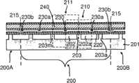
图2A是cMUT结构的横截面图,示出完整的cMUT元件200和每侧一个的相邻的cMUT元件200A和200B的部分。cMUT结构构造在衬底晶片201上,并也具有中间弹性层220和顶板240。衬底晶片201、中间弹性层220和顶板层240以下面的方式从底部排列到顶部:顶板层240的底侧面面向中间弹性层220的顶侧面且中间弹性层220的底侧面面向衬底晶片201的前侧面。cMUT元件200、200A和200B由穿过顶板240和中间弹性层220形成的分隔沟槽215分隔。2A is a cross-sectional view of a cMUT structure showing a
顶板240通过多个板弹簧连接器230、230a和230b连接到中间弹性层220。在某些实施例中,多个连接器230分布在装置元件区上。可根据应用的需要设计连接器的分布。众多的分布配置对于本发明都是可能的。The
图2B是所选择的cMUT部分210的放大图,它是完整的cMUT元件200的一部分。所选择的cMUT部分210是完整的cMUT元件200(和其它cMUT元件200A和200B)的基本单元。所选的cMUT部分210的结构提供了理解完整的cMUT元件200的基础。FIG. 2B is an enlarged view of a selected
如图2B所示,所选择的cMUT部分210包括以从顶部至底部穿过该结构的想象的垂直线(未示出)为中心的两个半部分。cMUT元件的基本结构构造在衬底201上,衬底具有支承特征部(在下文中称为“侧壁锚”)203,它具有在两个相对的侧上的两个侧壁,分别作为空腔202和202a的边界。支承特征部(侧壁锚)203可以是作为形成空腔202和202a的结果形成的衬底201的集成部分,但也可以是附加到分离衬底上的附加的结构。衬底201可以由诸如硅和多晶硅之类的非导电材料或导电材料制成。在侧壁锚203是分隔结构的构造中,侧壁锚203的导电率可与衬底201的导电率相同或不同。例如,衬底201可由非导电材料制成而侧壁锚203是诸如金属、硅或多晶硅之类的导电材料。As shown in FIG. 2B, the selected
cMUT结构部分210还具有这些部件:中间弹性层220,它较佳的是弹性膜;位于中间弹性层220上的底电极225;位于中间弹性层220顶部的连接器230和230a;位于连接器230上的绝缘层235;通过介于其间的绝缘层235连接到连接器230和230a的顶板240;及顶电极250。The
取决于如何从cMUT元件200或从cMUT元件200的何处取得cMUT部分210,第二空腔202a可属于不同的和分隔的空腔,或仅仅是与空腔202相同的圆形或延伸空腔的另一部分。类似地,取决于如何从cMUT元件200或从cMUT元件200的何处取得cMUT部分210,第二连接器230a可以是不同的或分隔的连接器的一部分,或仅仅是与连接器230相同的圆形或延伸连接器的另一部分。Depending on how or where the
顶板240的底侧面面向中间弹性层220的顶侧面,而中间弹性层220的底侧面面向衬底晶片的前侧面,从而连接器230从中间弹性层220直立以在顶板240下限定换能空间260。换能空间260一般限定在顶板层240和侧壁锚203的顶面之间,但在图2B所示的构造中可用的换能空间260的实际高度由绝缘层235的厚度、底电极225的厚度以及中间弹性层220的厚度减小。应注意在某些实施例中可将顶板层240和侧壁锚203的顶面之间的整个高度用于换能空间260。The bottom side of the
连接器230和230a位于中间弹性层220上并且各自具有基本相同的连接器高度。连接器230和230a各自在水平方向上离开侧壁锚203的各侧壁足够的长度。这限定了各自锚固在侧壁锚203的各侧面上、具有背对背的双悬臂构造的两个悬臂。这些悬臂可通过各自的连接器(230或230a)在放置连接器(230或230a)的施力端(例如,左侧悬臂上的222)处激发。悬臂和各自的空腔202和202a实现连接器230和230a的垂直位移,这使顶板240以类似于活塞的运动基本垂直地运动,由此改变了换能空间260。当cMUT结构210的两个半部分以相同的相位运动时,进一步保证了垂直的类似于活塞的运动。
在所示的具体的例子中,侧壁锚203的顶面由中间弹性层220覆盖,弹性层进而由底电极225覆盖。此外,顶板240和连接器230不直接相互连接,而由其间的绝缘层235介于其间。因此顶板240和侧壁锚203的顶表面之间的换能空间260由中间弹性层220、底电极225和绝缘层235部分地占据。应注意,覆盖侧壁锚203的顶面的中间弹性层220、底电极225和绝缘层235的部分是可选的。在任何情况下,为了实现预期的能量转换,如果结构中包括额外的层,则换能空间260不应完全由这些额外的层占据。In the particular example shown, the top surface of the sidewall anchors 203 is covered by an intermediate
图2C是不同选择的cMUT部分211的放大图,它是完整的cMUT元件200的另一部分。与图2B中所示的所选择的cMUT部分210相比,所选的cMUT部分211从偏移的位置取得。所选择的cMUT部分211构造在衬底201上,它具有以两个相反侧面上的两个支承特征部(下文中称为“侧壁锚203和203a”)作为边界的空腔202。cMUT结构部分211还具有这些组件:中间弹性层220、位于中间弹性层220上的底电极225、位于中间弹性层220顶上的连接器230、位于连接器230上的绝缘层235、通过介入的绝缘层235连接到连接器230的顶板240和顶电极250。FIG. 2C is an enlarged view of a different selection of the
连接器230(也在图2中示出)位于中间弹性层上,并在水平方向上离开两个侧壁锚203和侧壁锚203m的侧壁。侧壁锚203和侧壁锚203m之间的中间弹性层220限定了在侧壁锚203和侧壁锚203m处锚固的双悬臂。双悬臂在位置222处头对头地连接,在位置222处放置连接器230以形成桥。Connectors 230 (also shown in FIG. 2 ) are located on the middle elastic layer and away from the sidewalls of the two sidewall anchors 203 and 203m in the horizontal direction. The intermediate
顶板240位于连接器230上,连接器230将顶板240与中间弹性层220分隔以在顶板下限定换能空间260。双悬臂和空腔202实现连接器230的垂直位移,这基本垂直地移动顶板240,因此改变换能空间并激活用于能量转换的换能器的换能构件。The
新颖的cMUT结构基本去除了将cMUT元件分为单元并需要在每一个cMUT单元的周界支承并夹紧膜的单元绝缘壁的常规的概念。图1所示的常规的cMUT设计-包括美国专利第7,030,536号中公开的具有柔性绝缘壁的cMUT设计,那些设计都需要在每一个cMUT单元的周界处的单元绝缘壁(例如,图1中的单元绝缘壁18或美国专利第7,030,536号中公开的柔性单元绝缘壁)以限定cMUT单元并支承膜的周界。在由绝缘壁限定的周界内,底电极直接沉积在衬底上(图1)或沉积在与单元绝缘壁分隔的单个底座的顶部(美国专利第7,030,536号)(即,柔性支承结构)。The novel cMUT structure substantially removes the conventional concept of dividing cMUT elements into cells and requiring cell insulating walls that support and clamp membranes at the perimeter of each cMUT cell. Conventional cMUT designs shown in Figure 1 - including cMUT designs with flexible insulating walls disclosed in U.S. Patent No. 7,030,536, those designs require cell insulating walls at the perimeter of each cMUT cell (e.g., 18 or the flexible cell insulating wall disclosed in US Pat. No. 7,030,536) to define the cMUT cell and support the perimeter of the membrane. Within the perimeter defined by the insulating walls, the bottom electrode is deposited directly on the substrate (Fig. 1) or on top of a single pedestal separated from the cell insulating walls (US Patent No. 7,030,536) (ie, flexible support structure).
以图2A-2C所示的cMUT设计,cMUT元件不再需要分为单元因此不需要绝缘壁来限定单元周界。顶板层240和顶电极250由弹性结构(所示实施例中的多个悬臂)通过基于需要自由布置和分布的多个连接器来支承,因此将顶板240的整个负载有效分布在多个弹簧(悬臂)上。这解决了现有技术设计中固有的单元受限制的问题。中间弹性层220和底电极225由也可基于需要分布在整个衬底晶片201上的多个侧壁锚203支承,而不限于外围区域。With the cMUT design shown in FIGS. 2A-2C , the cMUT element no longer needs to be divided into cells and thus no insulating walls are required to define the cell perimeter. The
以此设计,可形成具有很大的活动区域的cMUT元件。cMUT元件的工作频率不仅可由用于顶板240的材料的选择来调节而且可由多个悬臂的构造-包括各个悬臂的弹性强度和cMUT元件的区域中悬臂分布密度情况-来调节。活动面积可显著大于关于常规的cMUT结构可能达到的活动面积。衬底晶片201上形成的整个顶板240可以是可移动的,而没有任何夹紧或固定的区域。如果期望的话,多个cMUT元件可通过形成穿过顶板240的分隔沟槽215来形成。在某些构造中,抑制沟槽也可切穿中间弹性层220。然而,原则上,具有很大的活动面积的整个cMUT结构可用作单个cMUT元件。With this design, a cMUT element with a large active area can be formed. The operating frequency of the cMUT element can be adjusted not only by the choice of material for the
此外,以图2A和图2B中的cMUT结构设计,可将顶板240分隔成相同或不同尺寸和形状的多个较小的顶板。每一个较小的顶板可作为单个cMUT元件来寻址,或者可将多个较小的顶板结合起来并作为单个cMUT元件来寻址。In addition, with the cMUT structure design in FIGS. 2A and 2B , the
此外,与常规cMUT中在其边缘(或柱)处夹紧的柔性膜不同,可将图2A和图2B中示出的顶板240设计成柔性或刚性的。以刚性顶板,可包括任何数量的分隔的较小的顶板240的cMUT的整个表面可移动。Furthermore, the
正如在本文确认的几篇其它专利申请中详细公开的,侧壁203及其对应的连接器230可自由分布在衬底晶片201上。相应地形成的悬臂可以是相同尺寸和相同的弹性强度或各种不同的期望的尺寸和弹性强度。悬臂也可均匀地或根据期望的图案分布在衬底晶片201上以达到某些特殊的效果。图2A和2B所示的cMUT结构的独特的设计具有解决现有技术cMUT设计遇到的很多问题的可能性。As disclosed in detail in several other patent applications identified herein, the
正如下文所述,以上的新颖的cMUT结构可利用本发明的方法来制造。As described below, the above novel cMUT structures can be fabricated using the method of the present invention.
制造工艺取决于每一层的材料选择。例如,硅、玻璃、石英或蓝宝石可用作衬底。可选择硅、多晶硅、氮化硅、氧化物、LTO、SiC、金刚石、聚对二甲苯、PMMA、PDMS、聚合物、金属或其它工艺兼容材料作为用于中间弹性层和顶板的材料。氧化物和氮化硅、SiC、PDMS或聚对二甲苯可用作介电材料。以用于选择的各种材料,可选择不同的薄膜沉积和晶片接合技术(例如,硅熔融接合、阳极接合、共晶接合、热压和玻璃料接合)用于制造本发明的cMUT。The manufacturing process depends on the choice of materials for each layer. For example, silicon, glass, quartz or sapphire can be used as a substrate. Silicon, polysilicon, silicon nitride, oxide, LTO, SiC, diamond, parylene, PMMA, PDMS, polymer, metal or other process compatible materials can be chosen as materials for the middle elastic layer and the top plate. Oxide and silicon nitride, SiC, PDMS or parylene can be used as dielectric materials. With various materials for selection, different thin film deposition and wafer bonding techniques (eg, silicon fusion bonding, anodic bonding, eutectic bonding, thermocompression, and frit bonding) can be selected for fabricating the cMUTs of the present invention.
下面说明用于制造上述cMUT的制造工艺的例子。步骤的变体、组合及顺序的变化是可能的,而不背离本发明的精神。即使对于给定的例子,也有选择不同的材料和处理方法来实现每一步骤的自由。An example of a manufacturing process for manufacturing the cMUT described above will be described below. Variations, combinations and changes in the order of steps are possible without departing from the spirit of the invention. Even for a given example, there is freedom to choose different materials and treatments to achieve each step.
I.用于制造微机电装置的基本元件的制造方法I. Fabrication methods for the basic components used in the manufacture of microelectromechanical devices
根据本发明的一个方面,按照本发明用于制造微机电装置的方法可包括以下步骤:According to one aspect of the present invention, a method for manufacturing a microelectromechanical device according to the present invention may include the following steps:
(1)在衬底晶片的前侧面上形成至少一个空腔,其中每一个空腔具有含有顶面的至少一个侧壁;(1) forming at least one cavity on the front side of the substrate wafer, wherein each cavity has at least one sidewall containing a top surface;
(2)在中间弹性层的顶侧面或顶板层的底侧面上形成至少一个期望高度的连接器;以及(2) forming at least one connector of a desired height on the top side of the middle elastic layer or the bottom side of the top sheet layer; and
(3)接合衬底晶片、中间弹性层和顶板使得顶板的底侧面面向中间弹性层的顶侧面而中间弹性层的底侧面面向衬底的前侧面。(3) The substrate wafer, the intermediate elastic layer, and the top plate are bonded such that the bottom side of the top plate faces the top side of the intermediate elastic layer and the bottom side of the intermediate elastic layer faces the front side of the substrate.
接合后,可获得诸如图2A和2B所示的诸如电容式微加工超声换能器(cMUT)之类的微机电结构。由此制造的结构具有用于转换能量的可移动机械部件,即由悬臂垂直移动的顶板。After bonding, a microelectromechanical structure such as a capacitive micromachined ultrasound transducer (cMUT) such as that shown in Figures 2A and 2B can be obtained. The resulting structure has a movable mechanical part for converting energy, namely a top plate moved vertically by a cantilever.
应意识到,以上的步骤可按任何顺序发生并且它们物理上互相兼容以实现最后的结构。此外,接合衬底晶片、中间弹性层和顶板的步骤不意味着这三层必需在一个步骤中同时接合。它也不意味着这三层在没有任何介入的材料的情况下互相直接接触地接合在一起,还不表示这三层必需恰好以该特定的顺序接合。接合的任何组合和顺序都在本文的描述的含义内,只要在最后的结构中,顶板的底侧面面向中间弹性层的顶侧面,且中间弹性层的底侧面面向衬底晶片的前侧面,使得所述的期望的结构是可能的。It should be appreciated that the above steps may occur in any order and that they are physically compatible with each other to achieve the final structure. Furthermore, the step of bonding the substrate wafer, the middle elastic layer and the top plate does not mean that these three layers must be bonded simultaneously in one step. It also does not mean that the three layers are bonded together in direct contact with each other without any intervening materials, nor does it mean that the three layers must be bonded in exactly that particular order. Any combination and sequence of bonding is within the meaning of the description herein as long as in the final structure the bottom side of the top plate faces the top side of the middle elastic layer and the bottom side of the middle elastic layer faces the front side of the substrate wafer such that The desired configurations described are possible.
正如以下将要说明的,形成空腔和连接器的步骤可利用各种技术来实现,诸如根据期望的图案直接去除或添加材料,通过引入并随后去除牺牲层,或这两种技术的组合。As will be explained below, the steps of forming cavities and connectors can be accomplished using various techniques, such as direct removal or addition of material according to a desired pattern, by introducing and subsequently removing a sacrificial layer, or a combination of these two techniques.
此外,应意识到以下描述的很多步骤是可选的,包括但不限于在说明书中明确指定为可选的哪些步骤。Furthermore, it should be appreciated that many of the steps described below are optional, including but not limited to those steps expressly designated as optional in the specification.
(1)利用晶片接合技术的制造:(1) Manufacture using wafer bonding technology:
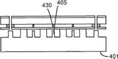
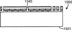
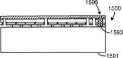
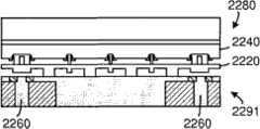
图3.1-3.9示出利用晶片接合技术的制造方法的例子。以下描述制造方法的步骤。在例子中,可将中间弹性层称为膜层。Figures 3.1-3.9 show examples of manufacturing methods using wafer bonding techniques. The steps of the manufacturing method are described below. In an example, the middle elastic layer may be referred to as a film layer.
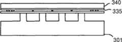
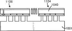
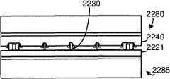
工艺以用作衬底晶片301的导电硅晶片开始。导电衬底晶片301可适用于用作换能器的底电极。The process starts with a conductive silicon wafer used as a
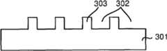
在步骤1中(图3.1),利用硅化物衬底图案化和蚀刻技术来在衬底晶片301上形成空腔302。每一个空腔由至少一个侧壁303限定。空腔302和侧壁303限定膜层的图案(在本说明书中一般可将其称为中间弹性层)。In step 1 (FIG. 3.1), a
在步骤2中(图3.2),绝缘体上的硅(SOI)晶片380与衬底晶片301接合。SOI晶片380包括厚的支承层382和和携带将成为膜层的薄层320的氧化物层384。厚的支承层382向薄层320提供支承用于在工艺期间的处理。如果接合在真空室中进行,则在该步骤中空腔是真空密封的。In step 2 ( FIG. 3.2 ), a silicon-on-insulator (SOI)
在步骤3中(图3.3),将接合的晶片在高温下退火,然后通过蚀刻去除支承层382和氧化物层384,以在侧壁303和空腔302的顶侧留下膜层320。如果需要的话,可在该步骤中在选择的膜区中进行硅掺杂。In step 3 ( FIG. 3.3 ), the bonded wafer is annealed at high temperature, then the
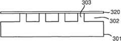
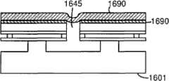
在步骤4中(图3.4),利用热氧化生长和图案化在膜层320的顶部形成连接器330。较佳的是,取代单独地形成分立的连接器330,所有的连接器330在一个步骤中通过形成图案化热氧化物层来形成。氧化物层限定了连接器330的高度,连接器330进而部分限定了膜层320上的换能空间的尺寸。应注意,图3.4和该组中的其它的图是横截面图。连接器330在表面的俯视图中可以是任何形状。连接器330可以是单独的纽扣状物,但也可以是长的线段,或连续的类似于环的形状。In step 4 (FIG. 3.4), a
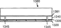
在步骤5中(图3.5),将另一个SOI晶片385在真空下接合在连接器330上并高温退火。SOI晶片385具有支承层386和携带将成为顶板层340的层的氧化物层387。SOI晶片385还可携带可选的薄的绝缘层335。可选的薄绝缘层335可生长在某层的顶部的SOI晶片385上,该层在SOI晶片385接合到膜层320上之前作为顶板层340的前身。或者,可选的薄绝缘层335可在最初的晶片(未示出)上生长然后接合到膜层335上。In step 5 (FIG. 3.5), another
在步骤6中(图3.6),通过蚀刻去除支承层386和氧化物层387以形成顶板层340。或者,在步骤5中使用最初的晶片以携带薄绝缘层335,则将最初的晶片研磨并抛光至期望的厚度以形成顶板层340。In step 6 ( FIG. 3.6 ),
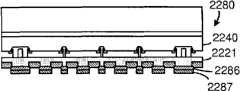
在可选的步骤中(图3.6A),将顶板层340蚀刻至所示的期望的形状或结构。此外,如果需要的话可在该步骤中可用期望的材料以期望的密度掺杂顶板层340。可进行硅和氧化物蚀刻以蚀刻穿过顶板层340和绝缘层335的通孔以从顶部到达底电极(通孔未示出)。或者,达到底电极的互连可利用由共同申请人在同一日期提交的本文确认的几篇专利申请中公开的穿过晶片的互连技术来形成。In an optional step (FIG. 3.6A), the
在步骤7中(图3.7),沉积并图案化金属层以形成顶电极355。In step 7 ( FIG. 3.7 ), a metal layer is deposited and patterned to form a
在可选的步骤中(图3.7A),将顶板层340图案化以形成孔342,以使顶板层340成为空心结构。如果需要的话,空心结构(顶板层340)中的孔342可用具有期望性质的材料再次填充或密封。In an optional step (FIG. 3.7A), the
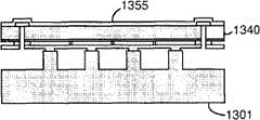
在步骤8中(图3.8),穿过顶板层340形成分隔沟槽345以分隔cMUT元件。In step 8 (FIG. 3.8), separation trenches 345 are formed through the
在步骤9中(图3.9),如果需要的话形成无源层346。In step 9 (FIG. 3.9), a
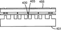
图4.1-4.9示出利用晶片接合技术的制造方法的另一个例子。该工艺以用作衬底晶片401的导电硅衬底开始。可采用导电衬底晶片401用作换能器的底电极。Figures 4.1-4.9 show another example of a manufacturing method using wafer bonding technology. The process starts with a conductive silicon substrate used as a
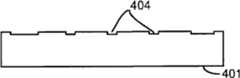
在准备步骤中(图4.1A),在衬底晶片401上形成凹槽404以在将形成的膜层和运动制动器之间限定间隙。运动制动器将设置用于cMUT表面板的位移的上限。In a preparatory step (FIG. 4.1A),
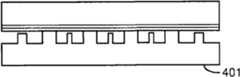
在步骤1中(图4.1B),利用硅蚀刻图案化衬底晶片401以形成由侧壁403限定的空腔402。还在空腔402中形成比侧壁403短的柱405。In step 1 ( FIG. 4.1B ), the
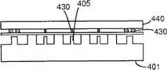
在步骤2至步骤8中(图4.2-4.8),进行几乎与图3.2-3.8所述的工艺流程相同的工艺流程以制造具有运动制动器405的cMUT结构。In
在图4.2-4.8中所示的工艺流程还说明了对图3.2-3.8所示的工艺流程的几个变化。在步骤5和步骤6中(图4.5-4.6),示出SOI晶片485不具有顶板层440上的氧化层,结果顶板层440位于连接器430上而没有类似于图3.5-3.6中的335的介入的氧化物层。The process flow shown in Figures 4.2-4.8 also illustrates several variations to the process flow shown in Figures 3.2-3.8. In
短于侧壁403的柱405是以上工艺的附加特征。柱405形成于空腔402中以用作运动制动器。应意识到,柱405也可利用本文所述的其它制造工艺来形成。此外,尽管柱405可利用单独的工艺来形成,但它们较佳地通过适当设计的图案化与形成空腔402和侧壁403的同时形成。各种化学或机械方法可用于该构造。
此外,如图4.8中完成的cMUT结构所示,连接器430中的每一个都在对应的柱405的正上方形成。该特殊的构造对于用作运动制动器的柱405具有优化的效果,因为连接器430所在的位置最有可能作出最大垂直位移。Furthermore, each of the
除硅熔融接合外,其它的晶片接合技术(例如,阳极接合、共晶接合、热压和玻璃料接合)可用于在本发明中以类似的方式构造诸如cMUT之类的微机电结构。不同的材料和适当的接合技术可用于构造每一层。例如,在利用共晶接合或阳极接合的工艺中,玻璃或蓝宝石以及硅可用作衬底材料。取代利用SOI晶片中的硅层来形成膜层和板层,可在载体晶片(例如,硅晶片、玻璃晶片或蓝宝石晶片)上生长或沉积具有期望性质的薄膜层或多薄膜层(例如,氮化硅、LTO、金刚石、SiC、聚酰亚胺、PMMA、PDMS和聚合物)。可将具有期望的一个或多个薄膜层的载体晶片接合到具有期望的结构的其它的晶片上以形成微机电结构的膜层和顶板。因为上述的工艺一般需要较低的工艺温度,所以它们有益于稍后不期望高温的工艺步骤(例如,换能器和集成电路的集成)。In addition to silicon fusion bonding, other wafer bonding techniques (eg, anodic bonding, eutectic bonding, thermocompression, and frit bonding) can be used to similarly fabricate microelectromechanical structures such as cMUTs in the present invention. Different materials and appropriate bonding techniques can be used to construct each layer. For example, glass or sapphire as well as silicon can be used as substrate materials in processes utilizing eutectic bonding or anodic bonding. Instead of utilizing silicon layers in SOI wafers to form layers and slabs, thin-film layers or multiple thin-film layers (e.g., nitrogen silicon carbide, LTO, diamond, SiC, polyimide, PMMA, PDMS, and polymers). A carrier wafer with a desired thin film layer or layers may be bonded to other wafers with desired structures to form the membrane layers and top plate of the MEMS structure. Because the processes described above generally require lower process temperatures, they are beneficial for later process steps where high temperatures are not desired (eg, integration of transducers and integrated circuits).
图5.1-5.9示出利用晶片接合技术的制造方法的另一个例子。该方法是图3.1-3.9和图4.1-4.8的方法的稍有变化的方法。例如,在该方法的实施例中,连接器形成于顶板的底侧面上,膜层位于连接器上,然后将顶板和膜层放置在衬底晶片的顶部以覆盖形成于衬底晶片上的空腔。以下参考图5.1-5.9示出该方法的步骤。Figures 5.1-5.9 show another example of a manufacturing method using wafer bonding techniques. This approach is a slight variation of the approach of Figures 3.1-3.9 and Figures 4.1-4.8. For example, in an embodiment of the method, the connectors are formed on the bottom side of the top plate, the film is positioned over the connectors, and then the top plate and film are placed on top of the substrate wafer to cover the voids formed on the substrate wafer. cavity. The steps of this method are shown below with reference to Figures 5.1-5.9.
在步骤1中(图5.1),该工艺以SOI晶片580开始。SOI晶片580具有将在后面的工艺步骤中成为cMUT的顶板层540的期望的硅层。氧化物层531生长在硅顶板层540上。或者,该工艺也可以最初的晶片(未示出)开始,将其研磨并抛光至与后面的步骤中的cMUT顶板层相同的期望的厚度。In step 1 ( FIG. 5.1 ), the process starts with an
在步骤2中(图5.2),将氧化物层531图案化以形成板-膜连接器530。可选地,生长另一薄氧化物层535作为绝缘层,并且也可按照需要将其图案化。In step 2 ( FIG. 5.2 ), the
在步骤3中(图5.3),将SOI晶片580与另一SOI晶片590接合,SOI晶片590具有支承层592和薄氧化物层594并携带期望的膜层520。In step 3 ( FIG. 5.3 ), the
在步骤4中(图5.4),去除SOI晶片590的厚支承层592和薄氧化物层594以留下通过连接器530与顶板层540接合的膜层520。In step 4 ( FIG. 5.4 ), thick support layer 592 and thin oxide layer 594 of SOI wafer 590 are removed to leave
在步骤5中(图5.5A-E),可采用各种选择的工艺。图5.5A中示出了第一选择,其中将具有由侧壁503A限定的空腔502A的最初晶片501A通过膜层520和连接器530接合到SOI晶片580。这完成了基本的cMUT结构,该结构类似于利用本文所述的其它方法制造的结构。In step 5 (Fig. 5.5A-E), various alternative processes can be used. A first option is shown in FIG. 5.5A , where an
步骤5的第二选择在图5.5B中示出。硅熔融接合用于接合具有形成于其中的穿过晶片的互连506和图案化空腔502B的衬底晶片501B。根据该选择所得的cMUT结构类似于图5.5A中的结构,但具有构造在内部的穿过晶片的互连506,穿过晶片的互连506可提供如由共同申请人在同一日期提交的本文确认的几篇专利申请中详细描述的一些另外的优点。The second option for
步骤5的第三选择在图5.5C(C_1和C_2)中示出。如图5.5C_1所示,在膜层520上沉积并图案化适当的金属层511(或其它的粘附层)。在图5.5C_2中,将具有穿过晶片的互连506及由图案化侧壁503C限定的图案化空腔502C的衬底晶片501C通过金属层511接合到cMUT结构的上部。金属层511的图案可较佳地匹配侧壁503C的图案。A third option for
步骤5的第四选择在图5.5D中示出,其中cMUT结构的上部接合到具有由金属材料形成的图案化侧壁503D的晶片501D上。还可将金属材料图案化以覆盖用作cMUT结构的电极512的部分的区域。例如,电极512可用作如由共同申请人提交的本文中确认的几篇专利申请中公开的具有两个层叠的电容器的cMUT结构中的第三电极。具有诸如侧壁503D和底电极512之类的图案化特征的金属材料层可以是具有期望的电路的PCB板上的结构。在该设计中,衬底晶片501D自身可以不导电并由诸如玻璃、蓝宝石或具有绝缘层的硅之类的材料制成。A fourth option of
步骤5的第五选择在图5.5E中示出,其中cMUT结构的上部接合到具有集成电路(IC)513的衬底晶片501E上,以实现cMUT换能器之间的集成。A fifth option for
在以上的步骤5后,可按照与图3.6-3.9中的步骤6至步骤9相同的步骤完成制造。After
或者,在该工艺中,分隔装置元件的深沟槽可在这些顶层接合到衬底晶片501之前从底部至顶部穿过膜层520和顶板层540来形成,而不是在顶层接合到衬底晶片501之后从顶部至底部形成。这将在后面的关于用于密封沟槽的技术的部分中进一步描述。Alternatively, in this process, the deep trenches separating the device elements can be formed from bottom to top through the
(2)利用牺牲技术的制造(2) Manufacture using sacrificial technology
取代通过从晶片直接去除材料形成空腔,衬底晶片上的空腔和中间弹性层上的空腔(限定换能空间)中的任一个或两者可利用牺牲技术来形成。连接器也可利用牺牲技术通过填充形成于随后被去除的牺牲层上的临时空腔来形成。Instead of forming the cavities by removing material directly from the wafer, either or both the cavities on the substrate wafer and the cavities on the intermediate elastic layer (defining the transducing volume) can be formed using sacrificial techniques. Connectors can also be formed using sacrificial techniques by filling temporary cavities formed in a sacrificial layer that is subsequently removed.
利用牺牲技术制造微机电装置的示例性方法包括以下步骤:An exemplary method of fabricating a microelectromechanical device using sacrificial techniques includes the following steps:
(1)提供具有前侧面和背侧面的衬底晶片;(1) providing a substrate wafer having a front side and a back side;
(2)在衬底晶片的前侧面上沉积第一牺牲层;(2) depositing a first sacrificial layer on the front side of the substrate wafer;
(3)图案化第一牺牲层以形成第一临时空腔;(3) patterning the first sacrificial layer to form a first temporary cavity;
(4)在第一牺牲层上沉积第一薄膜材料以填充第一临时空腔并进一步形成覆盖第一牺牲层的顶面的膜层,可选地,膜层具有用于通向下面的第一牺牲层的至少一个孔;(4) Deposit the first film material on the first sacrificial layer to fill the first temporary cavity and further form a film layer covering the top surface of the first sacrificial layer. at least one hole of a sacrificial layer;
(5)在膜层的顶部沉积第二牺牲层;(5) Depositing a second sacrificial layer on top of the film layer;
(6)图案化第二牺牲层以形成第二临时空腔;(6) patterning the second sacrificial layer to form a second temporary cavity;
(7)沉积第二薄膜材料以至少填充第二临时空腔;(7) depositing a second film material to at least fill the second temporary cavity;
(8)去除第一牺牲层和第二牺牲层以在衬底晶片的顶部形成第一空腔并在膜层的顶部形成第二空腔;以及(8) removing the first sacrificial layer and the second sacrificial layer to form a first cavity at the top of the substrate wafer and a second cavity at the top of the film layer; and
(9)将顶板设置在膜层上以从顶板和侧壁的顶面之间的第二空腔限定换能空间。(9) The top plate is disposed on the film layer to define the transduction space from the second cavity between the top plate and the top surface of the side wall.
在所得的结构中,第一空腔由具有顶面的至少一个侧壁限定。侧壁由沉积在第一临时空腔中的第一薄膜材料制成。第二空腔由膜层顶部上的至少一个连接器限定。连接器由沉积在第二临时空腔中的第二薄膜材料制成。类似于利用本文所述其它方法制造的微机电结构,在此处制造的所得的结构中,连接器从膜层直立并在水平方向上离开第一空腔的侧壁足够的距离以限定锚固在侧壁上的悬臂,以允许连接器的垂直位移,由此连接器的垂直位移以类似于活塞的运动基本垂直地移动顶板,从而改变换能空间。In the resulting structure, the first cavity is defined by at least one side wall having a top surface. The sidewalls are made of a first thin film material deposited in the first temporary cavity. The second cavity is defined by at least one connector on top of the membrane layer. The connector is made of a second film material deposited in the second temporary cavity. Similar to MEMS structures fabricated using other methods described herein, in the resulting structure fabricated here, the connectors are upstanding from the membrane layer and horizontally spaced a sufficient distance from the sidewall of the first cavity to define anchoring in the Cantilevers on the side walls to allow vertical displacement of the connector, whereby the vertical displacement of the connector moves the top plate substantially vertically in a piston-like motion, thereby changing the transducing volume.
图6.1-6.12示出利用牺牲技术的制造方法的例子。该工艺基于表面微加工。以下示出该方法的步骤。Figures 6.1-6.12 show examples of fabrication methods using sacrificial techniques. The process is based on surface micromachining. The steps of this method are shown below.
在步骤1中(图6.1),工艺以导电硅晶片601开始。沉积并图案化第一牺牲层661(例如,氧化物、SOG、金属、聚酰亚胺、聚合物或光刻胶层)。第一牺牲层661的图案将部分限定将形成的膜层的形状。在选择的区域662,将牺牲层661减薄至期望的厚度以在后面的步骤中用作牺牲蚀刻和密封通道。In step 1 ( FIG. 6.1 ), the process starts with a
在步骤2中(图6.2),沉积第一薄膜材料(例如,氮化硅、多晶硅、氧化物、硅、聚酰亚胺和聚合物)以形成膜层620。薄膜材料还填充了空隙621以成为在后面的步骤中限定悬臂的侧壁603。In step 2 ( FIG. 6.2 ), a first thin film material (eg, silicon nitride, polysilicon, oxide, silicon, polyimide, and polymer) is deposited to form a
在步骤3中(图6.3),可选地,通过蚀刻在膜层622上形成多个蚀刻孔622,以连接膜层620下的第一牺牲层661和将形成于膜层620上的第二牺牲层。In step 3 (FIG. 6.3), optionally, a plurality of
在步骤4中(图6.4),在膜层620的顶部沉积第二牺牲层611。In step 4 ( FIG. 6.4 ), a second
在步骤5中(图6.5),将第二牺牲层611图案化以具有开口613,来限定将在下一步骤中形成的膜-板连接器。膜层620上的图案化的第二牺牲层611在去除后还限定了换能空间。应意识到,步骤4和步骤5可像一个步骤那样同时进行,尤其是在第一牺牲层661和第二牺牲层611是相同材料或不同材料但具有兼容的去除特性时。In step 5 (FIG. 6.5), the second
在步骤6中(图6.6),沉积第二薄膜材料(例如,氮化硅或氧化物)以填充开口613以形成连接器630。薄膜沉积还选择地形成了绝缘层635。In step 6 ( FIG. 6.6 ), a second thin film material (eg, silicon nitride or oxide) is deposited to fill opening 613 to form connector 630 . Thin film deposition also optionally
在步骤7中(图6.7),穿过绝缘层635和在步骤2中沉积的薄膜材料蚀刻通孔641,以进入在步骤1(图6.1)的第一牺牲图案化中形成的牺牲蚀刻烛煤662。或者,可在所选的位置穿过绝缘层635蚀刻通孔以直接进入牺牲层661。In step 7 (FIG. 6.7),
在步骤8中(图6.8),通过蚀刻去除第一牺牲层661和第二牺牲层611。In step 8 (FIG. 6.8), the first
在步骤9中(图6.9),在去除牺牲层661和611后,进行另一个薄膜沉积以密封通孔641。在该步骤中,可进行另外的蚀刻以将绝缘层635减薄至适当的厚度,可将顶电极(将在下一步中沉积)令人满意地布置在那里。In step 9 ( FIG. 6.9 ), after removing the
在步骤10中(图6.10),在期望的位置沉积金属层以形成顶电极625。在该步骤中,如果需要的话,可蚀刻另外的通孔以接入底电极。In step 10 ( FIG. 6.10 ), a metal layer is deposited at the desired location to form the
在步骤11中(图6.11),在顶电极625的顶部沉积期望厚度的另一种薄膜材料(例如,氮化硅、LTO、金刚石、聚酰亚胺、聚合物、PDMS或PMMA)以形成顶板层640。In step 11 (FIG. 6.11), another thin film material (e.g., silicon nitride, LTO, diamond, polyimide, polymer, PDMS, or PMMA) is deposited to a desired thickness on top of the
在步骤12中(图6.12),在cMUT元件之间形成深沟以分隔元件。这也打开了进入换能器的引线接合焊盘(未示出)的通道。In step 12 (Fig. 6.12), deep trenches are formed between the cMUT elements to separate the elements. This also opens access to the wire bond pads (not shown) of the transducer.
应意识到,在以上的工艺中,除在连接器630的顶部形成绝缘层635外或取代在连接器630的顶部形成绝缘层635,可在膜层620的顶部形成绝缘层。这两个绝缘层是可选的。It should be appreciated that in the above process, an insulating layer may be formed on top of the
还应意识到,在以上的工艺中,取代形成蚀刻通道641,可使用多孔膜来提供用于蚀刻牺牲层的蚀刻通道。例如,在步骤6中(图6.6),取代沉积绝缘层635,可沉积多孔膜来填充开口613以形成连接器630。可通过穿过多孔膜的微孔的蚀刻去除牺牲层661。在牺牲层蚀刻后,可进行薄膜沉积以密封微孔。It should also be appreciated that in the above process, instead of forming the
(3)利用晶片接合技术和牺牲层技术的结合的制造(3) Manufacture using a combination of wafer bonding technology and sacrificial layer technology
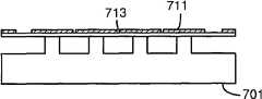
也可结合上述方法的两种类型的实施例。例如,衬底上的空腔的形成可利用牺牲技术来完成,而连接器的形成和其它步骤可利用热氧化生长和晶片接合技术来完成。相反,后者可利用牺牲技术来完成,而前者利用直接的材料去除和晶片接合技术。It is also possible to combine the two types of embodiments of the methods described above. For example, the formation of cavities on the substrate can be accomplished using sacrificial techniques, while the formation of connectors and other steps can be accomplished using thermal oxidative growth and wafer bonding techniques. Instead, the latter can be accomplished using sacrificial techniques, while the former utilizes direct material removal and die bonding techniques.
图7.1-7.11示出了结合了晶片接合技术和牺牲技术的示例性制造方法。该工艺以导电硅晶片开始,可将该导电硅晶片实现为换能器的底电极。Figures 7.1-7.11 illustrate an exemplary fabrication method combining wafer bonding and sacrificial techniques. The process starts with a conductive silicon wafer, which can be realized as the bottom electrode of the transducer.
在步骤1中(图7.1),用硅蚀刻图案化衬底晶片701,以形成空腔702和侧壁703,它们一起限定了膜图案和用于将形成的悬臂的锚。In step 1 (FIG. 7.1), the
在步骤2中(图7.2),将图案化衬底晶片701与具有厚的支承层782、绝缘层784和期望的膜层720的SOI晶片780接合。这可在真空下进行。在晶片接合过程中,SOI晶片780的膜层720面向图案化硅衬底晶片701。如果接合在真空室中进行,则空腔是真空密封的。将接合的晶片在高温下退火。In step 2 ( FIG. 7.2 ), the patterned
在步骤3中(图7.3),去除厚的支承层782和绝缘层784两者以留下膜层720。如果期望的话,可在选择的区域中高掺杂膜层720。In step 3 ( FIG. 7.3 ), both the
在步骤4中(图7.4),将牺牲层711沉积在膜层720上,并将其图案化以限定开口713,开口713将限定待形成的连接器。图案化牺牲层711还限定了将在膜层720和连接器上形成的换能空间。In step 4 ( FIG. 7.4 ), a
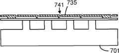
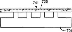
在步骤5中(图7.5),沉积薄膜材料(例如,氮化硅或氧化物)以填充开口713。开口713中填充的材料将成为连接器730。所沉积的薄膜材料还可形成绝缘层735。In step 5 ( FIG. 7.5 ), a thin film material (eg silicon nitride or oxide) is deposited to fill the
在步骤6中(图7.6),可蚀刻通孔714以进入牺牲层711。In step 6 ( FIG. 7.6 ), vias 714 may be etched into
在步骤7中(图7.7),然后去除牺牲层711。In step 7 (FIG. 7.7), the
在步骤8中(图7.8),在蚀刻牺牲层711后,进行薄膜沉积以密封通孔741。可进行深蚀以将绝缘层735减薄至期望的厚度,可将顶电极适当地布置在那里。In step 8 ( FIG. 7.8 ), after etching the
在步骤9中(图7.9),在期望的位置沉积金属层以形成顶电极725。在该步骤中,如果需要的话,可蚀刻通孔以进入底电极(通孔未示出)。In step 9 ( FIG. 7.9 ), a metal layer is deposited at the desired location to form the
在步骤10中(图7.10),在顶电极725的顶上沉积期望厚度的另一种薄膜材料(例如,氮化硅、LTO、金刚石、聚酰亚胺、聚合物、PDMS或PMMA)以形成顶板层740。In step 10 (FIG. 7.10), another thin film material (eg, silicon nitride, LTO, diamond, polyimide, polymer, PDMS, or PMMA) is deposited to a desired thickness on top of the
在步骤11中(图7.11),在cMUT元件之间形成沟槽745以分隔元件。这也打开了进入换能器的引线接合焊盘(未示出)的通道。In step 11 (FIG. 7.11),
在该工艺中,如果选择其它的衬底和膜材料则可采用其它的晶片接合方法(例如,共晶接合、阳极接合)。In this process, other wafer bonding methods (eg, eutectic bonding, anodic bonding) can be used if other substrate and film materials are selected.
对于具有多个元件的cMUT,如果需要的话可采用额外的工艺步骤来制成用于不同元件的分隔的底电极。For cMUTs with multiple elements, additional process steps may be used to make separate bottom electrodes for different elements, if desired.
图8.1-8.3示出利用晶片接合技术来分隔cMUT元件的底电极的工艺步骤。这些步骤在上述的其它步骤之前进行以准备衬底晶片。如图8.1所示,在最初晶片801b上生长绝缘层801a。如图8.2所示,将另一个最初晶片801c接合到经氧化的最初晶片801b上。然后将接合的晶片研磨并抛光至期望的厚度。如图8.3所示,在导电硅层801c上蚀刻沟槽809以将硅电分隔成将作为cMUT元件的底电极的图案化区域。提供经接合和处理的晶片作为衬底晶片801。然后以结合的衬底晶片801为开始进行如本文所述的装置制造步骤以制造cMUT结构。Figures 8.1-8.3 illustrate the process steps for separating the bottom electrodes of cMUT elements using wafer bonding techniques. These steps are performed prior to the other steps described above to prepare the substrate wafer. As shown in Figure 8.1, an insulating
图9.1-9.2示出将薄导电层用为底电极的分隔cMUT元件的底电极的工艺步骤。这些步骤可在上述的其它步骤前进行以准备衬底晶片。在图9.1中,首先将绝缘层901a沉积在硅晶片901b上。在图9.2中,将具有期望的厚度的薄导电层901c沉积在绝缘层901a上。然后将导电层901c图案化以按元件的需要形成底电极,来形成衬底晶片901。然后以衬底晶片901为开始进行如本文所述的装置制造步骤以制造cMUT结构。Figures 9.1-9.2 illustrate the process steps for separating the bottom electrodes of cMUT elements using a thin conductive layer as the bottom electrode. These steps may be performed prior to the other steps described above to prepare the substrate wafer. In Fig. 9.1, an insulating
以上的工艺也可与由共同申请人在同一日期提交的本文确认的几篇其它专利申请中公开的穿过晶片的互连技术结合。The above process may also be combined with through-wafer interconnection techniques disclosed in several other patent applications identified herein filed by the common applicant on the same date.
尽管利用cMUT结构示出了上述的制造方法,但该方法可用于制造具有用于转换能量的可移动机械部件的各种微机电装置。不管采用方法的哪一个实施例,所得的装置结构的特征在于顶板在连接器位置的垂直位移移动。换能构件可在微机电装置中形成或实现。例如,可将导电层引入到顶板中以用作cMUT结构中的顶电极,或者导电顶板由于其固有的导电性可实现为顶电极。可采用基于不同的能量转换方案的各种换能构件,但根据本发明的换能构件一般通过顶板的垂直移动在或顶板和中间弹性层(在cMUT结构的背景中示出的膜层)之间限定的换能空间的变化来实现能量转换。Although the fabrication method described above is illustrated using a cMUT structure, the method can be used to fabricate various microelectromechanical devices having movable mechanical parts for converting energy. Regardless of which embodiment of the method is employed, the resulting device structure is characterized by vertical displacement movement of the top plate at the connector location. The transducing member may be formed or implemented in a microelectromechanical device. For example, a conductive layer can be introduced into the top plate to serve as the top electrode in a cMUT structure, or a conductive top plate can be implemented as the top electrode due to its inherent conductivity. Various transducing members based on different energy conversion schemes can be used, but the transducing members according to the present invention are generally between either the top plate and the middle elastic layer (membrane layer shown in the context of the cMUT structure) by vertical movement of the top plate Energy conversion can be realized by changing the transduction space defined between them.
对于cMUT结构,必需具有顶电极和底电极。前者可在顶板之中或之上形成或实现,而后者可在中间弹性层或衬底晶片之中或之上形成。对于诸如pMUT和mMUT之类的不需要形成电容器的一对电极的其它类型的微机电装置,适当的换能构件可位于可移动的顶板或可移动的中间弹性层之中或之上。For a cMUT structure, it is necessary to have top and bottom electrodes. The former can be formed or implemented in or on the top plate, while the latter can be formed in or on the middle elastic layer or the substrate wafer. For other types of microelectromechanical devices, such as pMUTs and mMUTs, that do not require a pair of electrodes forming a capacitor, suitable transducing members may be located in or on a movable top plate or a movable middle elastic layer.
II.连接和互连的设计和制造II. Design and Fabrication of Connections and Interconnects
诸如换能器之类的微机电装置需要电连接以执行其功能。例如,换能器的可移动表面(诸如,本文所示的顶板)可能需要电连接到固定的焊盘(例如,引线接合焊盘)以与外部接口。在某些换能器设计中cMUT中的元件之间的顶电极可能需要电互连在一起,尤其是对于2D阵列。对于连接结构有很多可能的设计,但连接到可移动部件的连接一般应柔软(或柔性)并足够导电,使得它们对装置性能具有最小的影响。Microelectromechanical devices such as transducers require electrical connections to perform their functions. For example, a movable surface of a transducer (such as the top plate shown herein) may need to be electrically connected to fixed pads (eg, wire bond pads) to interface with the outside. Top electrodes between elements in a cMUT may need to be electrically interconnected together in certain transducer designs, especially for 2D arrays. There are many possible designs for the connection structure, but the connections to the movable parts should generally be soft (or flexible) and conductive enough that they have minimal impact on device performance.
以下描述了根据本发明的换能器连接设计的几个例子。Several examples of transducer connection designs according to the invention are described below.
在第一类型的构造中,在用于制造装置(例如,cMUT)的同一工艺步骤中以适当的掩模设计形成连接或互连。In a first type of construction, the connections or interconnections are formed with appropriate mask designs in the same process step used to fabricate the device (eg, cMUT).
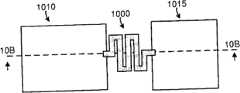
图10A和10B示出换能器元件和连接锚之间的连接的例子。图10A是换能器元件1010和锚固的连接焊盘1015之间的连接1000的俯视图。图10B是图10A所示的同一结构的横截面图。如图所示,接近换能器元件1010的区域可用于构造用作接口的锚固的连接焊盘1015。锚固的连接焊盘1015由下面的支承锚1021支承并连接到下面的支承锚1021(图10B)。锚固的连接焊盘1015和支承锚较佳地被分隔并且不受换能元件的悬臂和可移动顶板层1040的运动的影响。Figures 10A and 10B show examples of connections between transducer elements and connection anchors. FIG. 10A is a top view of a
换能元件1010和锚固的连接焊盘1015均构造在相同的衬底晶片1001上,并与同一多层制造工艺兼容,尽管对两部分的图案化不同以具有不同的内部结构。在所示的例子中,在换能元件1010和锚固的连接焊盘1015之间的连接1000通过图案化导电层1055形成于顶板1040上。为了使连接1000柔软并有弹性,将连接1000的导电路径做得很薄或以锯齿形缠绕。不仅在晶片表面尺寸上(如图10A的俯视图所示)还在晶片深度尺寸上(如图10B中的横截面视图所示)形成薄的连接1000的导电路径。例如,连接1000仅包括顶层(导电层1055和顶板层1040)的一部分而包括衬底1001的一部分。Both the
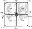
图11A和11B示出换能元件之间的互连的例子。图11A是通过锚固的连接焊盘1112、1114、1116和1118互连的四个换能元件1102、1104、1106和1108的俯视图。图11B是同一结构的横截面图。尽管图10A所示的基本的元件锚固连接可用于其中的互连,但图11A和11B中的设计具有不同的排列以实现更紧凑的尺寸和较好的互连效率。如图所示,锚固的连接焊盘1112、1114、1116和1118位于由四个分别的换能元件1102、1104、1106和1108共用的共用拐角处。每一个换能器元件通过各自的细连接线1222、1224、1226或1228连接到各自的锚固连接焊盘,这些连接线较佳地在表面尺寸(水平)和晶片深度(垂直)尺寸上很细。取决于锚固的连接焊盘1112、1114、1116和1118怎样彼此电连接,可单独或共同寻址四个换能器元件1102、1104、1106和1108。另外的锚固连接焊盘1113、1115、1117和1119也包括在所选的拐角处,并可用于将所示的各换能器元件进一步连接到未示出的其它换能器元件。11A and 11B show examples of interconnections between transducing elements. 11A is a top view of four
以上的连接和互连方案的一个优点是不需要引入额外的工艺步骤来制作连接和互连结构。可作为用于制作换能器元件自身的制造工艺的一部分来制造所有的连接和互连结构。然而,如果期望的话,可引入额外的工艺步骤以减薄在连接或互连图案所处区域的顶板层1140以连接结构更加柔性。One advantage of the above connection and interconnection scheme is that no additional process steps need to be introduced to fabricate the connection and interconnection structures. All connections and interconnection structures may be fabricated as part of the fabrication process used to fabricate the transducer elements themselves. However, if desired, additional process steps may be introduced to thin the top plate layer 1140 in the region where the connection or interconnect patterns are located to make the connection structure more flexible.
在第二类型的构造中,在完成cMUT工艺后形成连接或互连。图12.1-12.4示出在用于制作诸如本文所述的cMUT结构之类的微机电装置的主要制造工艺后制造连接和互连的例子。In a second type of configuration, the connections or interconnects are formed after the cMUT process is completed. Figures 12.1-12.4 show examples of connections and interconnections fabricated after the main fabrication process used to fabricate microelectromechanical devices such as the cMUT structures described herein.
工艺以基本上完成的示例性cMUT结构1200开始。在步骤1中(图12.1),在cMUT结构1200的顶部上沉积牺牲材料1290(例如,光刻胶、聚酰亚胺、聚合物、PDMS和聚对二甲苯)以填充cMUT元件之间的沟槽或cMUT元件和锚固的连接焊盘之间的沟槽。在步骤2中(图12.2),深蚀牺牲材料1290以暴露cMUT的顶电极1255。在步骤3中(图12.3),沉积并图案化金属层1256以形成期望的连接或互连。在步骤4中(图12.4),选择地去除牺牲材料1290。The process begins with a substantially completed
或者,具有期望性质(诸如声学、机械或电)的材料可用于填充沟槽并保持在沟槽中。填充的材料不被去除并成为最后的换能器结构的补充部分以基于其性质提供期望的效果。Alternatively, a material with desired properties, such as acoustical, mechanical or electrical, may be used to fill and retain the trenches. Filled material is not removed and becomes a complementary part of the final transducer structure to provide the desired effect based on its properties.
III.用于密封装置元件之间的沟槽的技术III. Techniques for sealing grooves between device components
在某些应用中需要密封cMUT元件之间的沟槽。例如,密封结构可有助于防止介质或湿气泄漏入沟槽。可将密封结构设计成使元件之间的耦合最小化。密封结构还可提供元件之间的电连接。可在装置制造期间或之后密封沟槽。In some applications it is desirable to seal the trenches between cMUT elements. For example, a sealing structure can help prevent media or moisture from leaking into the trench. The sealing structure can be designed to minimize coupling between components. The sealing structure can also provide electrical connection between components. The grooves can be sealed during or after device fabrication.
图13.1-13.12示出在正常的装置制造过程中结合沟槽密封的制造方法的例子。在以下步骤中描述该工艺。Figures 13.1-13.12 show examples of fabrication methods incorporating trench sealing during normal device fabrication. The process is described in the following steps.
步骤1至步骤4(图13.1-13.4)与图5.1-5.4中描述的步骤1至4相同。简言之,在步骤1中(图13.1),工艺以SOI晶片1380开始。SOI晶片1380具有将在后面的工艺步骤中成为cMUT的顶板层的期望的硅层1340。氧化物层1331生长在硅层1340上。在步骤2中(图13.2),将氧化物层1331图案化以形成板-膜连接器1330。选择地,生长另一薄氧化物层1335作为绝缘层,并且如果需要的话,也可将其图案化。在步骤3中(图13.3),将SOI晶片1380与另一SOI晶片1390接合,SOI晶片1390具有支承层1392和携带期望的膜层1320的薄氧化物层1394。在步骤4中(图13.4),去除SOI晶片1390的厚支承层1392和薄氧化物层1394以留下以连接器1330与顶板层1340接合的膜层1320。如果需要的话,可在膜层1320的选择的区域中进行硅掺杂。
在步骤5中(图13.5),穿过膜层1320、绝缘层1335和顶板层1340形成沟槽1345以分隔cMUT元件。用于形成沟槽1345的蚀刻在SOI晶片1380的氧化物层1381处停止。In step 5 (FIG. 13.5),
在步骤6中(图13.6),可选地将膜层1320图案化以限定用于接触膜层1320和衬底晶片1301的接触位置1321。In step 6 ( FIG. 13.6 ), the
在步骤7中(图13.7),将具有图案化空腔1302和侧壁1303的硅衬底晶片1301在接触位置1321接合到膜层1320。在该步骤中可用各种接合技术来接合其它类型的衬底晶片。In step 7 ( FIG. 13.7 ), a
在步骤8中(图13.8),深蚀SOI晶片1380至氧化物层1381以形成包括顶板层1340和氧化物层1381的顶板晶片。如果需要的话可将顶板晶片图案化。在此阶段,沟槽1345可由氧化物层1381来密封。In step 8 ( FIG. 13.8 ), the
在步骤9中(图13.9),将氧化物层1381图案化,以为在下一步骤中将顶板层1340与顶电极接触作准备。如果需要的话,可通过适当的蚀刻工艺来减薄剩余的氧化物层1381。In step 9 (FIG. 13.9), the
在步骤10中(图13.10),将金属层沉积在顶板层1340和图案化氧化物层1381上以形成顶电极1355。In step 10 ( FIG. 13.10 ), a metal layer is deposited on
图14.1-14.16示出在正常的装置制造工艺后结合沟槽密封工艺的制造方法的例子。该工艺采用牺牲蚀刻技术。在以下的步骤中描述了该工艺。Figures 14.1-14.16 show an example of a fabrication method incorporating a trench sealing process after the normal device fabrication process. The process uses sacrificial etching techniques. The process is described in the following steps.
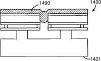
在步骤1中(图14.1),提供完成的cMUT晶片1400。沟槽1445分隔两个cMUT元件。In step 1 (FIG. 14.1), a completed
在步骤2中(图14.2),将牺牲层1490(例如,光刻胶、聚酰亚胺、聚合物、PDMS、LTO、TEOS或SOG)涂在完成的cMUT晶片1400的顶部。牺牲层1490可填充或部分填充沟槽1445。In step 2 ( FIG. 14.2 ), a sacrificial layer 1490 (eg, photoresist, polyimide, polymer, PDMS, LTO, TEOS, or SOG) is coated on top of the completed
在步骤3中(图14.3),利用平板印刷均匀地或选择地减薄牺牲层1490直到顶电极1455的至少一部分暴露。牺牲材料1491留在沟槽1445中。如果需要非均匀减薄则可采用掩模。In step 3 (FIG. 14.3), the
在步骤4中(图14.4),将具有期望的性质的另一金属层1492沉积在顶电极1455和留在沟槽1445中的牺牲材料1491上。如果需要每一个cMUT元件的顶电极1455单独寻址,则可使用介电材料(例如,聚酰亚胺、聚合物、PDMS、LTO、氮化硅、Teflon或Pyrelene)代替金属层1492。可将金属层1492图案化成期望的形状。也可在用于牺牲层蚀刻的金属层1492上形成通孔(图14.1-14.6中未示出,但图15.1-15.4中示出)。In step 4 ( FIG. 14.4 ), another
在步骤5中(图14.5),利用牺牲层蚀刻来去除剩余的牺牲材料1491。In step 5 (FIG. 14.5), the remaining
在步骤6中(图14.6),涂或滴下另一介电层1493(例如,聚酰亚胺、聚合物、LTO、氮化硅、Teflon、Pyrelene、SOG、PDMS、光刻胶、环氧树脂或蜡)以密封金属层1492上的通孔。如果需要的话,可将介电层1493图案化成期望的形状,或从cMUT的顶面去除介电层1493。In step 6 (FIG. 14.6), another dielectric layer 1493 (e.g., polyimide, polymer, LTO, silicon nitride, Teflon, Pyrelene, SOG, PDMS, photoresist, epoxy, etc.) is applied or dropped. or wax) to seal the vias on the
图15.1-15.4示出与上面相同的工艺,但示出具有包含在图中的通孔1595的装置结构的较大的部分。为了易于在后面的工艺步骤中密封,通孔1595可位于换能器元件的活动区域的外部。Figures 15.1-15.4 show the same process as above, but showing a larger portion of the device structure with vias 1595 included in the figures. For ease of sealing in later process steps, the via 1595 may be located outside the active area of the transducer element.
图15.1示出cMUT结构1500,它与示出整个装置结构的较大的部分的图14.1-14.6中的cMUT换能器相同。Figure 15.1 shows a
图15.2示出在工艺的步骤4(图14.4)中的cMUT换能器1500的状态。用剩余的牺牲材料1591填充沟槽1545。沉积具有期望性质(金属或其它介电膜)的层1592,以覆盖沟槽1545。图15.2还示出通过图案化形成的通孔1595以进入牺牲材料1591。Figure 15.2 shows the state of the
图15.3示出在通过牺牲层蚀刻去除牺牲材料1591后的状态。Figure 15.3 shows the state after removal of the
图15.4示出通孔1595已用适当的材料1593密封。Figure 15.4 shows that the through
可采用沟槽密封方法的其它变体。图16.1-16.4示出用具有期望性质的材料密封沟槽的另一种方法。Other variations of the trench sealing method may be used. Figures 16.1-16.4 illustrate another method of sealing the trench with a material having the desired properties.
在步骤1中(图16.1),将具有期望性质的材料(例如,聚酰亚胺、聚合物、PMMA、PDMS、SOG或环氧树脂)的层1690旋涂或喷涂在顶电极1635上以覆盖沟槽1645。例如,可期望对于硅表面干燥并具有高粘性的材料。也可利用薄的聚酰亚胺带(例如,各种Kapton带)、Teflon带或Parafilm(蜡)贴在cMUT的顶面上以覆盖沟槽1645来完成该步骤。In step 1 (FIG. 16.1), a
在步骤2中(图16.2),利用适当的蚀刻方法(例如,O2等离子蚀刻)将层1690减薄至期望的厚度。也可将层1690图案化成期望的形状,例如留下暴露的顶电极。剩余的图案化层1691继续覆盖沟槽1645。In step 2 (FIG. 16.2),
在步骤3中(图16.3),将金属层1692沉积在剩余的图案化层1691和暴露的顶电极1655上。可将金属层1692进一步图案化。In step 3 ( FIG. 16.3 ), a
在步骤4中(图16.4),如果需要的话,涂上并图案化另一个介电层1693(例如,聚酰亚胺、聚合物、PMMA、PDMS、SOG、环氧树脂、LTO、氮化硅、Teflon或Pyrelene)。In step 4 (FIG. 16.4), another
应意识到,除以上使用的沉积、涂、喷涂方法外,还可利用晶片接合技术来转移期望材料的膜。It should be appreciated that in addition to the deposition, coating, spraying methods used above, wafer bonding techniques may also be utilized to transfer films of desired materials.
图17.1-17.4示出利用晶片接合技术来将期望的膜从处理晶片转移到cMUT的方法。在步骤1中(图17.1),将期望的膜1791(例如,金属膜、聚酰亚胺、聚合物、LTO、氮化硅、Teflon、Pyrelene、SOG、光刻胶或环氧树脂)涂在适当的处理晶片1709(例如,硅或玻璃)上。在步骤2中(图16.2),用适当的接合技术(例如,共晶接合、热压接合、阳极接合或诸如环氧树脂之类的粘合层)来将携带期望的膜1791的处理晶片1709接合或粘合在cMUT 1700上。在步骤3中(图16.3),去除处理晶片1709,将膜1791留在cMUT 1700上。如果需要的话,还可将膜1791图案化至期望的形状。在步骤4中(图16.4),如果需要的话,可沉积并图案化另一个膜。Figures 17.1-17.4 illustrate a method of transferring a desired film from a handle wafer to a cMUT using wafer bonding techniques. In step 1 (FIG. 17.1), the desired film 1791 (e.g., metal film, polyimide, polymer, LTO, silicon nitride, Teflon, Pyrelene, SOG, photoresist, or epoxy) is coated on Appropriate processing on wafer 1709 (eg, silicon or glass). In step 2 (FIG. 16.2), the
可将另外的特征部引入沟槽区以进一步改进性能或实现某些特殊的效果。图18.1-18.2示出具有构造在cMUT元件之间的沟槽中的柱的cMUT结构。该图还示出密封这一沟槽的过程。Additional features can be introduced into the trench region to further improve performance or to achieve some special effect. Figures 18.1-18.2 illustrate cMUT structures with posts built in trenches between cMUT elements. The figure also shows the process of sealing this trench.
图18.1示出具有构造在分隔两相邻cMUT元件的沟槽1845中的柱1846的cMUT结构1800的横截面。添加柱1846以减小cMUT元件之间的交叉耦合。将柱1846锚固在衬底晶片1801上。可将沟槽1845内的柱1846的性质设计成最大限度减小cMUT元件之间的交叉耦合。可在cMUT工艺中制造柱1846而不需要任何额外的制造步骤。Figure 18.1 shows a cross-section of a
图18.2示出密封沟槽1845的层1892。层1892还可覆盖顶电极1855和柱1846。可采用上述密封cMUT元件之间的沟槽的相同的方法来密封沟槽1845。FIG. 18.2 shows
应意识到,可通过在包括某一层的每一个制造步骤适当设计的图案化在制造cMUT装置的同时制造柱1846。例如,可在形成侧壁1803的同一步骤中制造柱锚1847。为此,可用各种化学或机械方法。It should be appreciated that
IV.减小电接口焊盘上的寄生电容IV. Reduce the parasitic capacitance on the electrical interface pad
诸如所述的cMUT之类的微机电装置可能需要通过接合引线或探针互连到外部。为此,可能需要电接口焊盘(例如,引线接合焊盘或探针焊盘)。接口焊盘通常引入某些不期望的寄生参数(例如,寄生电容或电感)。为了改进换能器性能,需要将寄生参数最小化。MEMS devices such as the cMUT described may need to be interconnected to the outside by bond wires or probes. For this purpose, electrical interface pads (eg, wire bond pads or probe pads) may be required. Interface pads typically introduce certain undesirable parasitic parameters (eg, parasitic capacitance or inductance). In order to improve transducer performance, parasitic parameters need to be minimized.
一种减小寄生电容的方法是增加绝缘层(例如,诸如氧化物或氮化硅之类的介电层)的厚度。通常绝缘层的厚度受到由适当的工艺生长或沉积的介电层的厚度的限制。One way to reduce parasitic capacitance is to increase the thickness of the insulating layer (eg, a dielectric layer such as oxide or silicon nitride). Typically the thickness of the insulating layer is limited by the thickness of the dielectric layer grown or deposited by an appropriate process.
根据本发明的一个方面,公开了通过增加互连焊盘下的绝缘体的厚度来减小互连焊盘的寄生电容的方法。该方法使得衬底上的绝缘层的厚度由蚀刻深度而不是膜沉积的厚度限定,因此可制造绝缘体厚度显著大于利用膜沉积技术可能获得的厚度。According to one aspect of the present invention, a method of reducing parasitic capacitance of an interconnect pad by increasing the thickness of an insulator under the interconnect pad is disclosed. This approach enables the thickness of the insulating layer on the substrate to be defined by the etch depth rather than the film-deposited thickness, so insulator thicknesses significantly greater than are possible using film-deposition techniques can be fabricated.
该方法的一个实施例包括在将衬底晶片接合到顶板之前进行的以下的步骤:One embodiment of the method includes the following steps prior to bonding the substrate wafer to the top plate:
(1)在衬底晶片上形成绝缘空腔,其中图案化空腔具有期望的总厚度并位于适于形成用于拟被制造的微机电装置的附近的微机电元件的互连焊盘的位置。(1) Forming insulating cavities on a substrate wafer, wherein the patterned cavities have a desired overall thickness and are located at locations suitable for forming interconnection pads for microelectromechanical elements in the vicinity of the microelectromechanical device to be fabricated .
(2)用介电材料填充绝缘空腔以形成厚度与图案化空腔的总厚度相同的嵌入式绝缘体;以及(2) filling the insulating cavity with a dielectric material to form an embedded insulator having the same thickness as the total thickness of the patterned cavity; and
(3)在嵌入式绝缘体的顶部形成电互连焊盘。(3) Form electrical interconnection pads on top of the embedded insulator.
该方法的另一个实施例采用不同的工艺来实现类似的效果。具体地,取代如上所述形成平(无特征)的绝缘空腔,在衬底晶片上形成图案化空腔。在一个实施例中,图案化空腔具有插入了衬底的未去除的本体材料的实线的窄通道。图案化空腔具有期望的总厚度并位于适于形成用于拟被制造的微机电装置的附近的微机电元件的互连焊盘的位置。在形成图案化空腔后,将图案化空腔中的未去除的本体材料的实线氧化以形成厚度与图案化空腔的总厚度相同的嵌入式绝缘体。然后在嵌入式绝缘体的顶部形成电互连焊盘。Another embodiment of the method uses a different process to achieve a similar effect. Specifically, instead of forming flat (featureless) insulating cavities as described above, patterned cavities are formed on the substrate wafer. In one embodiment, the patterned cavity has narrow channels inserted with solid lines of unremoved bulk material of the substrate. The patterned cavity has a desired overall thickness and is located at a location suitable for forming interconnection pads for microelectromechanical elements in the vicinity of the microelectromechanical device to be fabricated. After the patterned cavity is formed, the solid lines of unremoved bulk material in the patterned cavity are oxidized to form an embedded insulator with the same thickness as the total thickness of the patterned cavity. Electrical interconnection pads are then formed on top of the embedded insulator.
在本发明的另一个方面中,可利用以上的方法将嵌入式绝缘体形成于装置结构的顶板中,而不是衬底晶片中。In another aspect of the present invention, the above method can be used to form embedded insulators in the top plate of the device structure, rather than in the substrate wafer.
图19.1-19.6示出通过在图案化空腔中形成厚的绝缘体来减小互连焊盘的寄生电容的方法的例子。可在cMUT制造前完成期望位置处的厚的绝缘层。该方法具有以下描述的步骤。Figures 19.1-19.6 show an example of a method of reducing the parasitic capacitance of an interconnect pad by forming a thick insulator in a patterned cavity. Thick insulating layers at desired locations can be done prior to cMUT fabrication. The method has the steps described below.
在步骤1中(图19.1),在衬底晶片1901的期望的位置处蚀刻图案化空腔1971。在所示的例子中,图案化空腔1971具有插入了未去除的衬底晶片材料1973的细线的空通道1972。In step 1 ( FIG. 19.1 ), patterned
可在形成厚度的绝缘体之后在同一衬底晶片1901上形成cMUT结构。图案化空腔1971具有期望的总厚度并位于适于形成用于拟被制造的微机电装置的附近的微机电元件的互连焊盘的位置。The cMUT structure may be formed on the
在步骤2中(图19.2),图案化空腔或被氧化或用期望的材料(例如,玻璃料、或SOG)填充以形成厚的绝缘体1974。In step 2 ( FIG. 19.2 ), the patterned cavity is either oxidized or filled with the desired material (eg, glass frit, or SOG) to form a
在步骤3中(图19.3),如果需要的话平坦化表面。In step 3 (Fig. 19.3), planarize the surface if necessary.
在步骤4中(图19.4),形成由侧壁1903限定的空腔1902。这些将用于诸如cMUT结构之类的微机电装置的构造。该装置制造可利用任何方法,包括本文所述的方法。In step 4 (Fig. 19.4), a cavity 1902 bounded by side walls 1903 is formed. These will be used in the construction of microelectromechanical devices such as cMUT structures. The device can be fabricated using any method, including those described herein.
在步骤5中(图19.5),形成或引入膜层1920到空腔1902和侧壁1903上。In step 5 ( FIG. 19.5 ), a
在步骤6中(图19.6),完成用于该装置(所示cMUT)的制造工艺以作出该装置。图19.6示出在衬底晶片1901上制造的与厚绝缘体1974相邻的cMUT元件1905。还可在装置制造过程中增加厚的绝缘体1974自身以成为完整的连接锚1906,连接锚1906可用于通过连接1907连接到cMUT元件1905,图10A和10B中示出了连接1907的一个例子。In step 6 (Fig. 19.6), the fabrication process for the device (cMUT shown) is completed to make the device. FIG. 19.6 shows a
图20.1-20.4示出通过在图案化空腔中形成厚的绝缘体来减小互连焊盘的寄生电容的方法的另一个例子。与图19.1-1.6所示的例子不同,在该例子中,可在cMUT制造后在期望的位置完成厚绝缘层。该方法具有下述的步骤。Figures 20.1-20.4 illustrate another example of a method of reducing parasitic capacitance of interconnect pads by forming thick insulators in patterned cavities. Unlike the example shown in Figures 19.1-1.6, in this example thick insulating layers can be done at desired locations after cMUT fabrication. The method has the following steps.
在步骤1中(图20.1),提供基本上完成的cMUT结构2000。如图20.1所示,cMUT制造工艺已经完成到在顶板层2040上形成表面层的步骤。In step 1 (FIG. 20.1), a substantially completed cMUT structure 2000 is provided. As shown in FIG. 20.1 , the cMUT manufacturing process has been completed to the step of forming a surface layer on
在步骤2中(图20.2),在顶板层2040上形成图案化空腔2071。图案化空腔2071具有插入了顶板层2040的未去除本体材料2073的实线的窄通道2072,而图案化空腔2071具有期望的总厚度并位于适于形成用于连接附近的微机电元件(例如,cMUT 2005)的互连焊盘的位置。如果需要的话,可向衬底晶片2001内蚀刻图案化空腔2071。In step 2 ( FIG. 20.2 ), patterned
在步骤3中(图20.3),氧化图案化空腔2071或用期望的材料(例如,玻璃料或SOG)填充图案化空腔2071以形成厚的绝缘体2074。In step 3 ( FIG. 20.3 ), the patterned
在步骤4中(图20.4),将金属层沉积在cMUT元件2005的顶部以形成顶电极2055。沉积并图案化相同的金属层以在厚绝缘体2074的顶部形成接触层2056。In step 4 ( FIG. 20.4 ), a metal layer is deposited on top of the
图19.1-19.6和图20.1-20.4中示出的示例性厚绝缘体构造用于具有嵌入式悬臂的cMUT。然而,形成厚绝缘层或厚绝缘体的这些方法可与需要锚固连接的任何其它微机电装置的制造工艺一起应用。The exemplary thick insulator configurations shown in Figures 19.1-19.6 and Figures 20.1-20.4 are used for cMUTs with embedded cantilevers. However, these methods of forming thick insulating layers or insulators can be applied with any other microelectromechanical device fabrication process that requires an anchored connection.
如以上的例子所示,本发明的用于减小寄生电容的方法的独特的方面是在衬底晶片或顶板上的绝缘层的厚度由蚀刻深度而不是膜沉积厚度限定,因此克服了由膜厚度施加的固有的限制。As shown in the above examples, a unique aspect of the method of the present invention for reducing parasitic capacitance is that the thickness of the insulating layer on the substrate wafer or top plate is defined by the etch depth rather than the film deposition thickness, thus overcoming the problem caused by the film deposition. Inherent limitations imposed by thickness.
V.制造具有附加特征部的微机电装置的制造方法V. METHOD OF MANUFACTURING MEMS DEVICES WITH ADDITIONAL FEATURES
构想了在微机电装置的基本元件上的附加特征部,并可利用下述方法来制造。Additional features on the base elements of the microelectromechanical device are contemplated and may be fabricated using the methods described below.
图21示出了特征是自对准悬臂的cMUT结构的横截面图。为了更清楚起见,图21省略了包含在各个分别的层和绝缘层中的诸如顶电极和底电极之类的某些可选部件。(正如本文所讨论的,尽管cMUT结构需要一对电极以形成电容器,但这些电极不必嵌入在各个分别的层中。)Figure 21 shows a cross-sectional view of a cMUT structure featuring self-aligned cantilevers. For greater clarity, FIG. 21 omits certain optional components, such as top and bottom electrodes, included in each respective layer and insulating layer. (As discussed herein, although a cMUT structure requires a pair of electrodes to form a capacitor, these electrodes do not have to be embedded in separate layers.)
图21的cMUT结构2111类似于图2C所示的cMUT部分211。cMUT结构2111构造在衬底2101上,并具有中间弹性层2120和顶板2140。空腔2102限定在衬底2101和中间弹性层2120之间。空腔2102以两个相对侧面上的两个侧壁锚2103和2103m为边界。连接器2130直立于中间弹性层2120的顶上,并连接到顶板2140。连接器2130在水平方向上离开两个侧壁锚2103和侧壁锚2103m的侧壁。侧壁锚2103和侧壁锚2103m之间的中间弹性层2120限定了在侧壁锚2103和侧壁锚2103m处锚固的双悬臂。双悬臂在放置连接器2130的位置处头对头地连接,以形成桥。顶板2140位于连接器2130上,连接器2130将顶板2140与中间弹性层2120分隔以在顶板2140下限定换能空间。双悬臂和空腔2102实现连接器2130的垂直位移,这基本垂直地移动顶板2140,因此改变换能空间并激活用于能量转换的换能器的换能构件。The cMUT structure 2111 of FIG. 21 is similar to the
在图2A-2C所示的cMUT结构中,采用具有基本均匀厚度的中间弹性层220,结果所形成的悬臂的梁的长度由对应的板-弹簧连接器230的位置220相对于各自的侧壁锚203或203m的边缘位置来确定。梁长度和对应的悬臂弹性强度的精确控制通过中间弹性层上的板-弹簧连接器的位置相对于各自的侧壁锚的位置的精确控制来实现。因为在板-弹簧连接器的制造方法的某些实施例中,在不同的平板印刷步骤中限定侧壁锚和空腔,实现这种精确控制可能有困难。这些不同的步骤中的任何对准差错可使悬臂长度离开其预期值。In the cMUT structure shown in FIGS. 2A-2C , an intermediate
与图2A-2C所示的cMUT结构不同,cMUT结构2111的特征是自对准悬臂。为了实现这一点,采用厚的中间弹性层2120。悬臂长度La和Lb由弹性膜层2120的各自的较薄的部分2124a和2124b限定。在所示的例子中,两较薄的部分2124a和2124b被由弹性膜层2120形成的桥中间的较厚的部分2122分隔。在本文所示的桥构造中,较厚的部分2122用作悬臂分割器。在其它构造中,较厚的部分2122可以是仅在一侧形成悬臂的末端的悬臂终端。两个锚固的较厚的部分2122a和2122b分别在两个侧壁锚2103和2103m的顶部,在某些实施例中,两个锚固的较厚的部分2122a和2122b形成两个侧壁锚2103和2103m的至少一部分,甚至形成整个侧壁锚2103和2103m。Unlike the cMUT structures shown in FIGS. 2A-2C , the cMUT structure 2111 features self-aligned cantilevers. To achieve this, a thick middle elastic layer 2120 is employed. Cantilever lengths La and Lb are defined by respective thinner portions 2124 a and 2124 b of elastic film layer 2120 . In the example shown, the two thinner portions 2124a and 2124b are separated by a thicker portion 2122 in the middle of the bridge formed by the elastic film layer 2120 . In the bridge configuration shown here, the thicker portion 2122 acts as a cantilever divider. In other configurations, the thicker portion 2122 may be a cantilever termination that forms the end of the cantilever on only one side. The thicker portions 2122a and 2122b of the two anchors are on top of the two sidewall anchors 2103 and 2103m respectively, and in certain embodiments, the thicker portions 2122a and 2122b of the two anchors form the two sidewall anchors 2103 and 2103m respectively. At least a portion of 2103m, or even the entirety of sidewall anchors 2103 and 2103m.
板-弹簧连接器2130位于较厚的部分2122上。在该构造中,悬臂长度La由在较厚的部分2122的边缘2106和较厚的部分2122a的边缘2104之间的距离限定。类似地限定悬臂长度Lb。因此可由平板印刷掩模预定悬臂长度La和Lb。连接器2130相对于中间弹性层2120(确切地说是较厚的部分2122)的任何未对准或中间弹性层2120(确切地说是其较厚的部分2122a和2122b)相对于侧壁锚2103或2103m的未对准将对悬臂长度及相应的悬臂的弹性强度具有最小的影响。在cMUT结构2111中的悬臂长度La和Lb及相应的悬臂的弹性强度因此几乎不或不依赖于各个制造步骤中的差异。Board-spring connectors 2130 are located on thicker portion 2122 . In this configuration, cantilever lengthLa is defined by the distance between edge 2106 of thicker portion 2122 and edge 2104 of thicker portion 2122a. The cantilever lengthLb is similarly defined. The cantilever lengths La and Lb can thus be predetermined by the lithographic mask. Any misalignment of the connector 2130 with respect to the middle elastic layer 2120 (specifically the thicker portion 2122) or the middle elastic layer 2120 (specifically its thicker portions 2122a and 2122b) with respect to the sidewall anchors 2103 or 2103m of misalignment will have minimal effect on the cantilever length and correspondingly the elastic strength of the cantilever. The cantilever lengths La and Lb in the cMUT structure 2111 and the corresponding elastic strength of the cantilever therefore have little or no dependence on differences in the individual fabrication steps.
在图21所示的横截面图的背景下给出了以上的描述。应意识到,在三维视图中,悬臂可以不是类似于梁的结构,而是如本文限定的区域或平面悬臂。例如,较薄的部件2124a和2124b可各自是延伸的带形或环形(轮环)形状。The above description has been given in the context of the cross-sectional view shown in FIG. 21 . It should be appreciated that in a three-dimensional view, the cantilever may not be a beam-like structure, but an area or planar cantilever as defined herein. For example, thinner members 2124a and 2124b may each be in the shape of an elongated ribbon or a ring (ring).
图22.1-22.16包括图22.14A-22.14D和图22.5a-22.5b示出用于制造具有自对准特征部的cMUT结构的晶片接合工艺。该工艺还可加入诸如沟槽密封之类的其它特征。以下描述工艺的步骤。Figures 22.1-22.16 including Figures 22.14A-22.14D and Figures 22.5a-22.5b illustrate a wafer bonding process for fabricating a cMUT structure with self-aligned features. The process can also incorporate other features such as trench sealing. The steps of the process are described below.
在步骤1中(图22.1),工艺以携带将成为最终的cMUT结构的顶板层2240的硅层2240的SOI晶片2280开始。在顶板2240的底部上生长氧化物层2281和氮化物层2282。或者,该步骤可以最初的晶片开始,可将最初的晶片研磨并抛光至在后面的步骤中用于顶板层的期望的厚度。In step 1 (FIG. 22.1), the process begins with an
在步骤2中(图22.2),根据cMUT设计图案化氧化物层2281和氮化物层2282以暴露顶板层2240的某些区域。In step 2 (FIG. 22.2), the
在步骤3中(图22.3),将顶板层2240的暴露区域氧化至期望的厚度。In step 3 (FIG. 22.3), the exposed areas of the
在步骤4中(图22.4),去除氮化物层和氧化物层,以在顶板层2240的底表面上形成凹槽2241。In step 4 ( FIG. 22.4 ), the nitride and oxide layers are removed to form
在步骤5中(图22.5),在顶板层2240的凹槽2241上形成图案化特征部2231。这些图案化特征部2231将成为最后的cMUT结构中的板-弹簧连接器2230的一部分。形成这一图案化特征部2231的一种方式是生长氧化物层。在此步骤中,可选择地执行各种附加步骤。在描述主要的步骤之后参考图22.5a-22.5b描述这些附加的步骤。In step 5 ( FIG. 22.5 ), patterned
在步骤6中(图22.6),在顶板层2240的凹槽2241上生长另一氧化物层2232。该可选的氧化物层2232可支承图案化特征部2231的根部并有助于使它们牢固地作为最后的cMUT结构的板-弹簧连接器2230的一部分。In step 6 ( FIG. 22.6 ), another
在步骤7中(图22.7),将携带硅层2221的另一SOI晶片2285结合到板-弹簧连接器2230。硅层22221将成为最后的cMUT结构中的中间弹性层2220以形成嵌入式弹簧(悬臂)。为了这个目的,硅层2221应具有适当的厚度。In step 7 ( FIG. 22.7 ), another
在步骤8中(图22.8),深蚀SOI晶片2285以去除载体层和氧化物层,以留下将成为中间弹性层2220的硅层2221。如果需要的话,可在该步骤中在硅层2221的选择的区域中进行硅掺杂。In step 8 ( FIG. 22.8 ), the
在步骤9中(图22.9),在硅层2221上形成并图案化氧化物层2286和氮化物层2287,使得能够到达硅层2221的选择的区域2288。In step 9 ( FIG. 22.9 ), an
在步骤10中(图22.10),将硅层2221的可到达区域2288氧化至期望的厚度。In step 10 (FIG. 22.10), the
在步骤11中(图22.11),在选择的位置处去除氧化物层和氮化物层,在硅层2221的区域2213的顶部上留下其余的氧化物和氮化物。区域2213将成为最后的cMUT结构中的侧壁锚2203。硅层2221的其它未覆盖的区域现在被暴露用于下一步骤。In step 11 ( FIG. 22.11 ), the oxide and nitride layers are removed at selected locations, leaving the remaining oxide and nitride on top of the
在步骤12中(图22.12),将硅层2221的暴露的区域氧化至期望的厚度。In step 12 (FIG. 22.12), the exposed regions of the
在步骤13中(图22.13),去除区域2213上的氧化物和氮化物层和在步骤12中形成的新氧化层,以形成具有将成为侧壁锚2203和悬臂分割器2222的较厚的部分特征部的中间弹性层2220。在该步骤(步骤13)后,有几种可用的选择。以下参考图22.14A描述第一选择,而一些其它的选择在后面参考图22.14B、22.14C和22.14C来描述。In step 13 (FIG. 22.13), the oxide and nitride layers on
在步骤14中(图22.14),结合具有期望的厚度的最初的晶片2201。该层成为用于最后的cMUT结构的衬底2201。此步骤后,完成制造的过程类似于本说明书中描述的某些其它示例性制造方法中的最后步骤。以下简要地描述一个例子。In step 14 (Fig. 22.14), an
在步骤15中(图22.15),深蚀顶部SOI晶片2280以去除载体层和氧化物层以形成顶板2240。In step 15 ( FIG. 22.15 ), the
在步骤16中(图22.16),如果需要的话,沉积并图案化金属层2250以形成互连。在各cMUT元件之间形成沟槽2215以分隔各个cMUT元件。In step 16 (FIG. 22.16), a metal layer 2250 is deposited and patterned to form interconnects, if desired. Trenches 2215 are formed between the cMUT elements to separate the individual cMUT elements.
几种其它的选择可用于以上的步骤14。在步骤14的第二选择中(图22.14B),取代接合最初的晶片,将具有形成于其中的穿过晶片的互连2260的经处理的晶片2291熔融接合到中间弹性层2220。经处理的晶片2291和中间弹性层2220限定空腔图案,该空腔图案对应于形成悬臂的区域的形状。还可用其它的晶片接合技术(例如,共晶接合、热压接合和阳极接合)来完成该步骤。Several other options are available for
在步骤14的第三选择中(图22.14C),将具有期望的金属图案或具有期望的电路的PCB板的晶片2292接合到中间弹性层2220。晶片2292可由诸如玻璃、蓝宝石或硅之类的材料制成。In a third option of step 14 ( FIG. 22.14C ), a wafer 2292 with the desired metal pattern or a PCB board with the desired circuitry is bonded to the intermediate
在步骤14的第四选择中(图22.14D),将具有构造于其中的集成电路2294(IC)的硅晶片2293接合到中间弹性层2220。In a fourth option of step 14 ( FIG. 22.14D ), a
在以上的步骤5中,可选择地进行几种附加步骤。参考图22.5a-22.5b描述这些附加步骤。在图22.5a中,穿过顶板2240形成沟槽2216以在顶板2240上分隔cMUT元件区。可执行该步骤代替上述的步骤16。在图22.5b中,如果需要的话,在沟槽2216中形成并处理薄膜材料2217。在这些额外的步骤之后,工艺继续进行到上述的步骤6。In
图23.1-23.7示出用于制造具有自对准特征部的cMUT结构的表面微加工工艺。该工艺还可加入诸如沟槽密封之类的其它特征部。以下描述该工艺的步骤。Figures 23.1-23.7 illustrate the surface micromachining process used to fabricate cMUT structures with self-aligned features. The process can also incorporate other features such as trench seals. The steps of this process are described below.
在步骤1中(图23.1),工艺以衬底晶片2301开始。在衬底晶片2301上沉积并图案化牺牲层2371。In step 1 ( FIG. 23.1 ), the process starts with a
在步骤2中(图23.2),在牺牲层2371上形成适当材料的层2329。层2329的材料还填充了牺牲层2371的图案。层2329将成为最后的cMUT结构的中间弹性层2320。In step 2 ( FIG. 23.2 ), a
在步骤3中(图23.3),利用表面微加工技术将层2329图案化以形成具有特征部的中间弹性层,特征部中的某些将成悬臂分割器2322。In step 3 ( FIG. 23.3 ),
在步骤4中(图23.4),将另一牺牲层2372沉积在中间弹性层2320上。In step 4 ( FIG. 23.4 ), another
在步骤5中(图23.5),将顶板层2340设置在牺牲层2372上。In step 5 ( FIG. 23.5 ), a
在步骤6中(图23.6),去除牺牲层2371和2372以形成空腔2302和2360。空腔2302在衬底2301的顶部以为cMUT结构中的悬臂提供位移空间。空腔2360在中间弹性层的顶部以用作cMUT结构的换能空间。如果需要的话可在该步骤中密封空腔。In step 6 ( FIG. 23.6 ),
在步骤7中(图23.7),如果期望的话可在顶板2340上沉积并图案化金属层2350。可形成沟槽以在该步骤中分隔cMUT元件。In step 7 (FIG. 23.7), a
用于以上图22.1-22.16和图23.1-23.7中所示的制造方法的每一步骤中的材料选择和工艺方法选择类似于本文中结合其它的微机电结构的制造方法所描述的材料选择和工艺方法选择。此外,尽管在上述的工艺中cMUT用于说明的目的,但该方法不限于此。微机电结构也可仅利用每一工艺的一部分来制造,或利用图22.1-22.16和图23.1-23.7中所示的工艺的不同的步骤顺序来制造。此外,取代利用SOI晶片,具有嵌入式弹簧的的微机电结构的中间弹性层可由具有高掺杂层的硅层或具有PN结层的硅层来制作。可随后利用选择的硅蚀刻来形成中间弹性层上的悬臂区域。The material selection and process selection for each step of the fabrication methods shown above in Figures 22.1-22.16 and Figures 23.1-23.7 are similar to those described herein in connection with other fabrication methods of MEMS structures Method selection. Furthermore, although a cMUT is used for illustrative purposes in the above process, the method is not limited thereto. MEMS structures can also be fabricated using only a portion of each process, or using a different sequence of steps of the processes shown in Figures 22.1-22.16 and Figures 23.1-23.7. Furthermore, instead of using an SOI wafer, the middle elastic layer of the MEMS structure with embedded springs can be made of a silicon layer with a highly doped layer or a silicon layer with a PN junction layer. A selective silicon etch can then be utilized to form the cantilever region on the middle elastic layer.
结合附图和示例性实施例详细描述了微机电装置的制造方法。本发明的方法提供了一种用于制造具有用于转换能量的可移动机械部件的各种微机电装置的具有潜在优点的制造方法,该方法尤其适合于制造电容式微加工超声换能器(cMUT),但也可用于制造具有用于转换能量的可移动的机械部件的其它的微机电装置。The manufacturing method of the MEMS device is described in detail with reference to the accompanying drawings and exemplary embodiments. The method of the present invention provides a potentially advantageous fabrication method for fabricating various microelectromechanical devices with movable mechanical parts for transforming energy, which is particularly suitable for fabricating capacitive micromachined ultrasonic transducers (cMUTs). ), but can also be used to make other microelectromechanical devices with movable mechanical parts for converting energy.
具体地,根据本发明的制造方法可用于制造和封装在名为“MICRO-ELECTRO-MECHANICAL TRANSDUCERS”代理机构案号为03004.03以及名为“MICRO-ELECTRO-MECHANICAL TRANSDUCERS”代理机构案号为03004.04的国际专利申请(PCT)中公开的新颖MUT,这些专利申请都由共同的申请人在同一日期提交,这些专利申请通过引用整体结合与此。In particular, the manufacturing method according to the present invention can be used to manufacture and package international patents under the name "MICRO-ELECTRO-MECHANICAL TRANSDUCERS" agency docket number 03004.03 and under the name "MICRO-ELECTRO-MECHANICAL TRANSDUCERS" agency docket number 03004.04 The novel MUT is disclosed in patent applications (PCT) all filed on the same date by common applicants, which are hereby incorporated by reference in their entirety.
在以上的说明中,参考其特定的实施例描述了本发明公开的内容,但本领域的技术人员将意识到本发明公开的内容不限于此。上述发明内容中的各个特征和方面可单独或结合地使用。此外,本发明内容可在除本文描述以外的很多种环境和应用中使用,而不背离说明书的较宽的精神和范围。我们要求专利保护落入所附权利要求的范围和精神内的各种修改和变化。因此,应将说明书和附图视为说明性的而不是限制性的。应意识到如本文所使用的术语“包括”、“包含”和“具有”明确地确定为开放式技术术语。In the above specification, the present disclosure has been described with reference to specific embodiments thereof, but those skilled in the art will appreciate that the present disclosure is not limited thereto. The various features and aspects in the above summary of the invention can be used alone or in combination. In addition, the present teachings may be used in numerous environments and applications other than those described herein without departing from the broader spirit and scope of the description. We claim patent protection for various modifications and changes that come within the scope and spirit of the appended claims. Accordingly, the specification and drawings are to be regarded as illustrative rather than restrictive. It should be appreciated that the terms "comprising", "comprising" and "having" as used herein are expressly intended to be open technical terms.
Claims (62)
Applications Claiming Priority (9)
| Application Number | Priority Date | Filing Date | Title |
|---|---|---|---|
| US68261905P | 2005-05-18 | 2005-05-18 | |
| US60/682,619 | 2005-05-18 | ||
| US69203805P | 2005-06-17 | 2005-06-17 | |
| US60/692,038 | 2005-06-17 | ||
| US70560605P | 2005-08-03 | 2005-08-03 | |
| US60/705,606 | 2005-08-03 | ||
| US74424206P | 2006-04-04 | 2006-04-04 | |
| US60/744,242 | 2006-04-04 | ||
| PCT/IB2006/051567WO2006123299A2 (en) | 2005-05-18 | 2006-05-18 | Methods for fabricating micro-electro-mechanical devices |
Publications (2)
| Publication Number | Publication Date |
|---|---|
| CN101578686Atrue CN101578686A (en) | 2009-11-11 |
| CN101578686B CN101578686B (en) | 2012-07-18 |
Family
ID=37431649
Family Applications (4)
| Application Number | Title | Priority Date | Filing Date |
|---|---|---|---|
| CN2006800171390AActiveCN101573861B (en) | 2005-05-18 | 2006-05-18 | Micro-electro-mechanical transducers |
| CNA2006800257832APendingCN101223633A (en) | 2005-05-18 | 2006-05-18 | Micro-electro-mechanical transducers |
| CN2006800226444AActiveCN101578686B (en) | 2005-05-18 | 2006-05-18 | Method of manufacturing a microelectromechanical device |
| CN2006800171371AActiveCN101589543B (en) | 2005-05-18 | 2006-05-18 | Micro-electro-mechanical transducers |
Family Applications Before (2)
| Application Number | Title | Priority Date | Filing Date |
|---|---|---|---|
| CN2006800171390AActiveCN101573861B (en) | 2005-05-18 | 2006-05-18 | Micro-electro-mechanical transducers |
| CNA2006800257832APendingCN101223633A (en) | 2005-05-18 | 2006-05-18 | Micro-electro-mechanical transducers |
Family Applications After (1)
| Application Number | Title | Priority Date | Filing Date |
|---|---|---|---|
| CN2006800171371AActiveCN101589543B (en) | 2005-05-18 | 2006-05-18 | Micro-electro-mechanical transducers |
Country Status (6)
| Country | Link |
|---|---|
| US (2) | US8105941B2 (en) |
| EP (1) | EP1883956A4 (en) |
| JP (1) | JP2008541473A (en) |
| CN (4) | CN101573861B (en) |
| CA (1) | CA2607885A1 (en) |
| WO (1) | WO2006123298A2 (en) |
Cited By (24)
| Publication number | Priority date | Publication date | Assignee | Title |
|---|---|---|---|---|
| CN102128641A (en)* | 2010-01-12 | 2011-07-20 | 佳能株式会社 | Capacitive detection type electro-mechanical transducer |
| CN102180441A (en)* | 2011-04-01 | 2011-09-14 | 上海丽恒光微电子科技有限公司 | Micro electromechanical device and manufacturing method thereof |
| CN103033699A (en)* | 2011-09-30 | 2013-04-10 | 意法半导体股份有限公司 | MEMS device, strip test method thereof and test strip thereof |
| CN103407958A (en)* | 2013-08-27 | 2013-11-27 | 上海先进半导体制造股份有限公司 | Production method of cavity-SOI (Silicon On Insulator) |
| CN104066520A (en)* | 2012-01-27 | 2014-09-24 | 皇家飞利浦有限公司 | Capacitive micromechanical transducer and method of manufacturing the same |
| CN104196650A (en)* | 2014-06-23 | 2014-12-10 | 西北工业大学 | Silicon-based MEMS array propeller and preparation method thereof |
| CN104701452A (en)* | 2013-12-04 | 2015-06-10 | 三星电子株式会社 | Capacitive micromachined ultrasonic transducer and method of fabricating the same |
| CN104812504A (en)* | 2012-11-20 | 2015-07-29 | 皇家飞利浦有限公司 | Capacitive micro-machined transducer and method of manufacturing the same |
| CN104934396A (en)* | 2014-03-21 | 2015-09-23 | 中芯国际集成电路制造(北京)有限公司 | Manufacturing method of bonding structure |
| CN105026905A (en)* | 2013-02-27 | 2015-11-04 | 德克萨斯仪器股份有限公司 | Capacitive mems sensor devices |
| CN105247890A (en)* | 2013-05-28 | 2016-01-13 | 罗伯特·博世有限公司 | Multilayer Composite Backplane for Micromechanical Microphones |
| CN106865483A (en)* | 2017-01-06 | 2017-06-20 | 中北大学 | Medical micro- electric capacity ultrasonic transducer face battle array probe and preparation method thereof |
| CN107305197A (en)* | 2016-04-21 | 2017-10-31 | 波音公司 | The apparatus and method for checking part |
| US10011476B1 (en) | 2016-12-29 | 2018-07-03 | Industrial Technology Research Institute | MEMS apparatus having impact absorber |
| CN109244232A (en)* | 2018-09-13 | 2019-01-18 | 徐景辉 | MEMS PZT (piezoelectric transducer) and production method |
| CN110267172A (en)* | 2019-06-28 | 2019-09-20 | Oppo广东移动通信有限公司 | Sound device, display device and terminal |
| CN110785374A (en)* | 2017-04-21 | 2020-02-11 | 弗劳恩霍夫应用研究促进协会 | MEMS transducer for interaction with a volume flow of a fluid and method of manufacturing the same |
| CN111151431A (en)* | 2018-11-08 | 2020-05-15 | 格芯新加坡私人有限公司 | Piezoelectric micromechanical ultrasonic transducer and method for producing same |
| CN111545438A (en)* | 2019-01-29 | 2020-08-18 | 韩国科学技术研究院 | Electrostatic Capacitive Micromachined Ultrasound Transducer |
| CN112047295A (en)* | 2019-06-07 | 2020-12-08 | 英飞凌科技股份有限公司 | Production of MEMS devices and MEMS devices with glass lids |
| CN112867690A (en)* | 2018-06-07 | 2021-05-28 | 恩赛特有限责任公司 | Miniature electrostatic motor and miniature mechanical force transmission device |
| CN112871613A (en)* | 2020-12-19 | 2021-06-01 | 复旦大学 | Piezoelectric micromachined ultrasonic transducer with support posts |
| CN113048974A (en)* | 2021-03-17 | 2021-06-29 | 吉林大学 | Bionic positioning device and using method thereof |
| CN113316486A (en)* | 2018-11-16 | 2021-08-27 | 维蒙股份公司 | Capacitive micromachined ultrasonic transducer and method of manufacturing the same |
Families Citing this family (96)
| Publication number | Priority date | Publication date | Assignee | Title |
|---|---|---|---|---|
| US7888709B2 (en) | 2004-09-15 | 2011-02-15 | Sonetics Ultrasound, Inc. | Capacitive micromachined ultrasonic transducer and manufacturing method |
| US8658453B2 (en) | 2004-09-15 | 2014-02-25 | Sonetics Ultrasound, Inc. | Capacitive micromachined ultrasonic transducer |
| WO2006123299A2 (en) | 2005-05-18 | 2006-11-23 | Kolo Technologies, Inc. | Methods for fabricating micro-electro-mechanical devices |
| EP1883956A4 (en) | 2005-05-18 | 2011-03-23 | Kolo Technologies Inc | Through-wafer interconnection |
| US7786592B2 (en) | 2005-06-14 | 2010-08-31 | John Trezza | Chip capacitive coupling |
| US7781886B2 (en) | 2005-06-14 | 2010-08-24 | John Trezza | Electronic chip contact structure |
| US7851348B2 (en) | 2005-06-14 | 2010-12-14 | Abhay Misra | Routingless chip architecture |
| US7560813B2 (en)* | 2005-06-14 | 2009-07-14 | John Trezza | Chip-based thermo-stack |
| US7687400B2 (en) | 2005-06-14 | 2010-03-30 | John Trezza | Side stacking apparatus and method |
| US7767493B2 (en) | 2005-06-14 | 2010-08-03 | John Trezza | Post & penetration interconnection |
| US7838997B2 (en) | 2005-06-14 | 2010-11-23 | John Trezza | Remote chip attachment |
| US7989958B2 (en) | 2005-06-14 | 2011-08-02 | Cufer Assett Ltd. L.L.C. | Patterned contact |
| US8456015B2 (en) | 2005-06-14 | 2013-06-04 | Cufer Asset Ltd. L.L.C. | Triaxial through-chip connection |
| WO2006134580A2 (en)* | 2005-06-17 | 2006-12-21 | Kolo Technologies, Inc. | Micro-electro-mechanical transducer having an insulation extension |
| US7786014B2 (en)* | 2006-09-22 | 2010-08-31 | Ipdia | Electronic device and method for making the same |
| JP4825778B2 (en)* | 2007-11-16 | 2011-11-30 | 株式会社日立製作所 | Semiconductor device and manufacturing method thereof |
| JP5337813B2 (en)* | 2007-12-03 | 2013-11-06 | コロ テクノロジーズ インコーポレイテッド | Dual-mode operation micromachined ultrasonic transducer |
| US7884015B2 (en)* | 2007-12-06 | 2011-02-08 | Micron Technology, Inc. | Methods for forming interconnects in microelectronic workpieces and microelectronic workpieces formed using such methods |
| JP2009181981A (en)* | 2008-01-29 | 2009-08-13 | Renesas Technology Corp | Manufacturing process of semiconductor device, and the semiconductor device |
| US8072079B2 (en)* | 2008-03-27 | 2011-12-06 | Stats Chippac, Ltd. | Through hole vias at saw streets including protrusions or recesses for interconnection |
| JP5473253B2 (en)* | 2008-06-02 | 2014-04-16 | キヤノン株式会社 | Structure having a plurality of conductive regions and manufacturing method thereof |
| KR101124857B1 (en)* | 2008-09-30 | 2012-03-27 | 주식회사 동부하이텍 | Image Sensor and Method for Manufacturing thereof |
| FR2938970A1 (en) | 2008-11-26 | 2010-05-28 | St Microelectronics Rousset | METHOD FOR STACKING AND INTERCONNECTING INTEGRATED CIRCUITS |
| SE533992C2 (en) | 2008-12-23 | 2011-03-22 | Silex Microsystems Ab | Electrical connection in a structure with insulating and conductive bearings |
| US8630033B2 (en) | 2008-12-23 | 2014-01-14 | Silex Microsystems Ab | Via structure and method thereof |
| US8729713B2 (en) | 2008-12-23 | 2014-05-20 | Silex Microsystems Ab | Via structure and method thereof |
| US8263492B2 (en)* | 2009-04-29 | 2012-09-11 | International Business Machines Corporation | Through substrate vias |
| JP5330115B2 (en) | 2009-06-17 | 2013-10-30 | 浜松ホトニクス株式会社 | Multilayer wiring board |
| US8324006B1 (en)* | 2009-10-28 | 2012-12-04 | National Semiconductor Corporation | Method of forming a capacitive micromachined ultrasonic transducer (CMUT) |
| US8563345B2 (en) | 2009-10-02 | 2013-10-22 | National Semiconductor Corporated | Integration of structurally-stable isolated capacitive micromachined ultrasonic transducer (CMUT) array cells and array elements |
| JP5473579B2 (en) | 2009-12-11 | 2014-04-16 | キヤノン株式会社 | Control device for capacitive electromechanical transducer and control method for capacitive electromechanical transducer |
| CN101844130A (en)* | 2010-05-14 | 2010-09-29 | 中国科学技术大学 | Array silicon micro-ultrasonic transducer and manufacturing method thereof |
| JP5570311B2 (en)* | 2010-06-07 | 2014-08-13 | キヤノン株式会社 | Electromechanical converter, specimen diagnostic device |
| DE102010029760B4 (en) | 2010-06-07 | 2019-02-21 | Robert Bosch Gmbh | Device with a via and method for its preparation |
| JP5702966B2 (en)* | 2010-08-02 | 2015-04-15 | キヤノン株式会社 | Electromechanical transducer and method for manufacturing the same |
| WO2012049825A1 (en)* | 2010-10-15 | 2012-04-19 | 日立オートモティブシステムズ株式会社 | Physical quantity detector |
| WO2012119333A1 (en)* | 2011-03-04 | 2012-09-13 | 中国科学院微电子研究所 | Through-silicon-via (tsv) structure and its fabricating method |
| US8486805B2 (en) | 2011-03-04 | 2013-07-16 | Institute of Microelectronics, Chinese Academy of Sciences | Through-silicon via and method for forming the same |
| US8519515B2 (en)* | 2011-04-13 | 2013-08-27 | United Microlectronics Corp. | TSV structure and method for forming the same |
| US8487410B2 (en) | 2011-04-13 | 2013-07-16 | Taiwan Semiconductor Manufacturing Company, Ltd. | Through-silicon vias for semicondcutor substrate and method of manufacture |
| JP5327279B2 (en)* | 2011-06-13 | 2013-10-30 | 株式会社デンソー | Ultrasonic sensor device |
| WO2013057642A1 (en) | 2011-10-17 | 2013-04-25 | Koninklijke Philips Electronics N.V. | Through-wafer via device and method of manufacturing the same |
| EP3689250B1 (en) | 2011-10-17 | 2022-12-07 | BFLY Operations, Inc. | Transmissive imaging and related apparatus and methods |
| DE102011085084B4 (en)* | 2011-10-24 | 2022-01-13 | Robert Bosch Gmbh | Method for producing an electrical via in a substrate and substrate with an electrical via |
| JP2013247139A (en)* | 2012-05-23 | 2013-12-09 | Ps4 Luxco S A R L | Semiconductor device and method of manufacturing the same |
| DE102012210033B4 (en)* | 2012-06-14 | 2023-02-02 | Robert Bosch Gmbh | Component with via and method of manufacture |
| KR101931358B1 (en)* | 2012-06-25 | 2018-12-31 | 삼성전자주식회사 | Jig and manufacturing method thereof and flip chip bonding method for chips composing ultrasound probe using jig |
| EP2922311A4 (en) | 2012-11-15 | 2016-08-03 | Olympus Corp | ULTRASONIC TRANSDUCER ELEMENT AND ULTRASOUND ENDOSCOPE |
| US9533873B2 (en) | 2013-02-05 | 2017-01-03 | Butterfly Network, Inc. | CMOS ultrasonic transducers and related apparatus and methods |
| US9351081B2 (en) | 2013-02-27 | 2016-05-24 | Texas Instruments Incorporated | Capacitive micromachined ultrasonic transducer (CMUT) with through-substrate via (TSV) substrate plug |
| US9520811B2 (en) | 2013-02-27 | 2016-12-13 | Texas Instruments Incorporated | Capacitive micromachined ultrasonic transducer (CMUT) device with through-substrate via (TSV) |
| US8883535B2 (en)* | 2013-02-28 | 2014-11-11 | Freescale Semiconductor Inc. | Microelectromechanical system devices having through substrate vias and methods for the fabrication thereof |
| US9041213B2 (en) | 2013-03-14 | 2015-05-26 | Freescale Semiconductor Inc. | Microelectromechanical system devices having through substrate vias and methods for the fabrication thereof |
| EP4122609B1 (en) | 2013-03-15 | 2024-11-06 | BFLY Operations, Inc. | Complementary metal oxide semiconductor (cmos) ultrasonic transducers and methods for forming the same |
| KR20220097541A (en) | 2013-03-15 | 2022-07-07 | 버터플라이 네트워크, 인크. | Monolithic ultrasonic imaging devices, systems and methods |
| US9667889B2 (en) | 2013-04-03 | 2017-05-30 | Butterfly Network, Inc. | Portable electronic devices with integrated imaging capabilities |
| EP3024594A2 (en) | 2013-07-23 | 2016-06-01 | Butterfly Network Inc. | Interconnectable ultrasound transducer probes and related methods and apparatus |
| JP2015023994A (en)* | 2013-07-26 | 2015-02-05 | セイコーエプソン株式会社 | Ultrasonic measurement device, ultrasonic head unit, ultrasonic probe, and ultrasonic imaging device |
| JP5490949B1 (en)* | 2013-08-08 | 2014-05-14 | 有限会社 ナプラ | Wiring board and manufacturing method thereof |
| WO2015071387A1 (en)* | 2013-11-18 | 2015-05-21 | Koninklijke Philips N.V. | Ultrasound transducer assembly |
| US9443758B2 (en)* | 2013-12-11 | 2016-09-13 | Taiwan Semiconductor Manufacturing Co., Ltd. | Connecting techniques for stacked CMOS devices |
| CN105828962B (en)* | 2013-12-12 | 2019-07-23 | 皇家飞利浦有限公司 | Single chip integrated three electrodes CMUT equipment |
| US9752943B2 (en)* | 2014-01-24 | 2017-09-05 | Infineon Technologies Dresden Gmbh | Sensor structures, systems and methods with improved integration and optimized footprint |
| EP3126065B1 (en) | 2014-03-31 | 2021-05-19 | Koninklijke Philips N.V. | Ic die, ultrasound probe, ultrasonic diagnostic system and method |
| AU2015247484B2 (en) | 2014-04-18 | 2020-05-14 | Butterfly Network, Inc. | Ultrasonic transducers in complementary metal oxide semiconductor (CMOS) wafers and related apparatus and methods |
| WO2015161157A1 (en) | 2014-04-18 | 2015-10-22 | Butterfly Network, Inc. | Architecture of single substrate ultrasonic imaging devices, related apparatuses, and methods |
| TWI643601B (en) | 2014-04-18 | 2018-12-11 | 美商蝴蝶網路公司 | Ultrasonic imaging compression method and device |
| US9067779B1 (en) | 2014-07-14 | 2015-06-30 | Butterfly Network, Inc. | Microfabricated ultrasonic transducers and related apparatus and methods |
| KR102363908B1 (en) | 2014-10-08 | 2022-02-17 | 삼성디스플레이 주식회사 | Stretchable films, methods of manufacturing the same and display devices including the same |
| GB2539368A (en) | 2015-02-09 | 2016-12-21 | Univ Erasmus Med Ct Rotterdam | Intravascular photoacoustic imaging |
| US10427188B2 (en) | 2015-07-30 | 2019-10-01 | North Carolina State University | Anodically bonded vacuum-sealed capacitive micromachined ultrasonic transducer (CMUT) |
| WO2017027789A1 (en) | 2015-08-12 | 2017-02-16 | Sonectics Ultrasound, Inc. | Method and system for measuring pressure using ultrasound |
| JP6649044B2 (en)* | 2015-11-10 | 2020-02-19 | 富士フイルム株式会社 | Ultrasonic endoscope and method of manufacturing ultrasonic endoscope |
| US10413938B2 (en) | 2015-11-18 | 2019-09-17 | Kolo Medical, Ltd. | Capacitive micromachined ultrasound transducers having varying properties |
| US9987661B2 (en) | 2015-12-02 | 2018-06-05 | Butterfly Network, Inc. | Biasing of capacitive micromachined ultrasonic transducers (CMUTs) and related apparatus and methods |
| EP3182445B1 (en)* | 2015-12-15 | 2020-11-18 | Nexperia B.V. | Semiconductor device and method of making a semiconductor device |
| EP3459465A4 (en)* | 2016-05-20 | 2020-01-15 | Olympus Corporation | Ultrasonic transducer module, ultrasonic endoscope, and method for manufacturing ultrasonic transducer module |
| US10618078B2 (en) | 2016-07-18 | 2020-04-14 | Kolo Medical, Ltd. | Bias control for capacitive micromachined ultrasonic transducers |
| US10399121B2 (en) | 2016-09-12 | 2019-09-03 | Kolo Medical, Ltd. | Bias application for capacitive micromachined ultrasonic transducers |
| CN108002339B (en)* | 2016-11-02 | 2019-12-31 | 中芯国际集成电路制造(上海)有限公司 | MEMS device and manufacturing method thereof |
| MY191544A (en)* | 2016-12-27 | 2022-06-30 | Intel Corp | Multi-conductor interconnect structure for a microelectronic device |
| CN106744642A (en)* | 2017-01-06 | 2017-05-31 | 中北大学 | The hybrid ultrasonic transducer face battle array probe of broadband and preparation method of receiving-transmitting balance |
| TWI637639B (en)* | 2017-02-14 | 2018-10-01 | 英屬開曼群島商智動全球股份有限公司 | Electro-acoustic transducer |
| US10196261B2 (en) | 2017-03-08 | 2019-02-05 | Butterfly Network, Inc. | Microfabricated ultrasonic transducers and related apparatus and methods |
| WO2018236956A1 (en) | 2017-06-21 | 2018-12-27 | Butterfly Network, Inc. | MICROFABRICATED ULTRASONIC TRANSDUCER HAVING INDIVIDUAL CELLS HAVING ELECTRICALLY ISOLATED ELECTRODE SECTIONS |
| US10613058B2 (en) | 2017-06-27 | 2020-04-07 | Kolo Medical, Ltd. | CMUT signal separation with multi-level bias control |
| JP2019039804A (en)* | 2017-08-25 | 2019-03-14 | セイコーエプソン株式会社 | MEMS device, electronic apparatus, and moving body |
| MY201172A (en)* | 2018-09-19 | 2024-02-08 | Intel Corp | Stacked through-silicon vias for multi-device packages |
| CN110518114B (en)* | 2019-07-31 | 2021-05-28 | 西安交通大学 | Frequency conversion self-focusing hybrid drive transceiver integrated PMUT unit and preparation method thereof |
| CN110508474B (en)* | 2019-07-31 | 2020-10-27 | 西安交通大学 | A hybrid drive MUT unit structure and its parametric excitation method |
| CN111182429B (en)* | 2020-01-03 | 2021-04-02 | 武汉大学 | High Fill Rate MEMS Transducers |
| IL294825A (en) | 2020-01-20 | 2022-09-01 | Univ Leland Stanford Junior | Labeled electrode and/or pulse wave excitation for a capacitive micromachined ultrasonic transducer |
| US11738369B2 (en)* | 2020-02-17 | 2023-08-29 | GE Precision Healthcare LLC | Capactive micromachined transducer having a high contact resistance part |
| CN111918188B (en)* | 2020-07-10 | 2021-12-14 | 瑞声科技(南京)有限公司 | MEMS loudspeaker and manufacturing process thereof |
| CN112718437B (en)* | 2020-12-16 | 2022-01-14 | 武汉大学 | Piezoelectric micromechanical ultrasonic transducer based on multi-diaphragm coupling |
| CN116891211A (en)* | 2022-04-01 | 2023-10-17 | 昇佳电子股份有限公司 | anchoring construct |
Family Cites Families (56)
| Publication number | Priority date | Publication date | Assignee | Title |
|---|---|---|---|---|
| US2975307A (en)* | 1958-01-02 | 1961-03-14 | Ibm | Capacitive prime mover |
| US4889832A (en)* | 1987-12-23 | 1989-12-26 | Texas Instruments Incorporated | Method of fabricating an integrated circuit with metal interconnecting layers above and below active circuitry |
| US4996627A (en)* | 1989-01-30 | 1991-02-26 | Dresser Industries, Inc. | High sensitivity miniature pressure transducer |
| JPH0365084A (en)* | 1989-08-02 | 1991-03-20 | Hitachi Ltd | Electrostatic secondary actuator, and optical head and optical disc device |
| US5146435A (en) | 1989-12-04 | 1992-09-08 | The Charles Stark Draper Laboratory, Inc. | Acoustic transducer |
| JPH0547916A (en)* | 1991-08-20 | 1993-02-26 | Fujitsu Ltd | Method for manufacturing semiconductor device |
| FR2700003B1 (en) | 1992-12-28 | 1995-02-10 | Commissariat Energie Atomique | Method for manufacturing a pressure sensor using silicon on insulator technology and sensor obtained. |
| US5894452A (en)* | 1994-10-21 | 1999-04-13 | The Board Of Trustees Of The Leland Stanford Junior University | Microfabricated ultrasonic immersion transducer |
| US5619476A (en)* | 1994-10-21 | 1997-04-08 | The Board Of Trustees Of The Leland Stanford Jr. Univ. | Electrostatic ultrasonic transducer |
| FR2744285B1 (en)* | 1996-01-25 | 1998-03-06 | Commissariat Energie Atomique | METHOD FOR TRANSFERRING A THIN FILM FROM AN INITIAL SUBSTRATE TO A FINAL SUBSTRATE |
| JP2000508860A (en) | 1996-04-18 | 2000-07-11 | カリフォルニア インスティチュート オブ テクノロジー | Thin film electret microphone |
| WO1999036824A1 (en)* | 1998-01-20 | 1999-07-22 | Seiko Epson Corporation | Optical switching device and image display device |
| US6002117A (en)* | 1998-03-10 | 1999-12-14 | Pak; Il Young | Electric heating cord with non-heating core-conducting element and reduced EMF emissions |
| US5917272A (en)* | 1998-06-11 | 1999-06-29 | Vectron, Inc. | Oven-heated crystal resonator and oscillator assembly |
| JP3532788B2 (en)* | 1999-04-13 | 2004-05-31 | 唯知 須賀 | Semiconductor device and manufacturing method thereof |
| JP4569167B2 (en)* | 1999-04-19 | 2010-10-27 | 株式会社村田製作所 | Manufacturing method of external force detection sensor |
| JP2001015721A (en)* | 1999-04-30 | 2001-01-19 | Canon Inc | Method for separating composite member and method for producing thin film |
| US6314057B1 (en) | 1999-05-11 | 2001-11-06 | Rodney J Solomon | Micro-machined ultrasonic transducer array |
| FR2805709B1 (en)* | 2000-02-28 | 2002-05-17 | Commissariat Energie Atomique | ELECTRICAL CONNECTION BETWEEN TWO FACES OF A SUBSTRATE AND METHOD OF MAKING |
| US6283601B1 (en)* | 2000-04-14 | 2001-09-04 | C Speed Corporation | Optical mirror system with multi-axis rotational control |
| EP1151962B1 (en)* | 2000-04-28 | 2007-06-13 | STMicroelectronics S.r.l. | Structure for electrically connecting a first body of semiconductor material overlaid by a second body of semiconductor material, composite structure using the electric connection structure, and manufacturing process thereof |
| US6646364B1 (en)* | 2000-07-11 | 2003-11-11 | Honeywell International Inc. | MEMS actuator with lower power consumption and lower cost simplified fabrication |
| US6467879B1 (en) | 2000-10-16 | 2002-10-22 | Xerox Corporation | Method and apparatus for preventing degradation of electrostatically actuated devices |
| US6512625B2 (en)* | 2000-11-22 | 2003-01-28 | Ball Semiconductor, Inc. | Light modulation device and system |
| US6558330B1 (en) | 2000-12-06 | 2003-05-06 | Acuson Corporation | Stacked and filled capacitive microelectromechanical ultrasonic transducer for medical diagnostic ultrasound systems |
| US6737740B2 (en)* | 2001-02-08 | 2004-05-18 | Micron Technology, Inc. | High performance silicon contact for flip chip |
| JP2002250665A (en) | 2001-02-23 | 2002-09-06 | Omron Corp | Capacitance-type sensor and its manufacturing method |
| US6600587B2 (en)* | 2001-04-23 | 2003-07-29 | Memx, Inc. | Surface micromachined optical system with reinforced mirror microstructure |
| JP4929538B2 (en)* | 2001-06-29 | 2012-05-09 | 株式会社デンソー | Manufacturing method of semiconductor device |
| US6585653B2 (en)* | 2001-07-31 | 2003-07-01 | Koninklijke Philips Electronics N.V. | Micro-machined ultrasonic transducer (MUT) array |
| JP4703061B2 (en)* | 2001-08-30 | 2011-06-15 | 富士通株式会社 | Thin film circuit board manufacturing method and via forming board forming method |
| US6750516B2 (en)* | 2001-10-18 | 2004-06-15 | Hewlett-Packard Development Company, L.P. | Systems and methods for electrically isolating portions of wafers |
| EP1351288B1 (en)* | 2002-04-05 | 2015-10-28 | STMicroelectronics Srl | Process for manufacturing an insulated interconnection through a body of semiconductor material and corresponding semiconductor device |
| US6767751B2 (en)* | 2002-05-28 | 2004-07-27 | Silicon Light Machines, Inc. | Integrated driver process flow |
| CN1250445C (en)* | 2002-06-25 | 2006-04-12 | 祥群科技股份有限公司 | Wafer level packaging device for MEMS components |
| US6958255B2 (en)* | 2002-08-08 | 2005-10-25 | The Board Of Trustees Of The Leland Stanford Junior University | Micromachined ultrasonic transducers and method of fabrication |
| US6822798B2 (en)* | 2002-08-09 | 2004-11-23 | Optron Systems, Inc. | Tunable optical filter |
| US6865140B2 (en)* | 2003-03-06 | 2005-03-08 | General Electric Company | Mosaic arrays using micromachined ultrasound transducers |
| US7443765B2 (en)* | 2003-03-06 | 2008-10-28 | General Electric Company | Reconfigurable linear sensor arrays for reduced channel count |
| SE526366C3 (en)* | 2003-03-21 | 2005-10-26 | Silex Microsystems Ab | Electrical connections in substrate |
| TW567355B (en)* | 2003-04-21 | 2003-12-21 | Prime View Int Co Ltd | An interference display cell and fabrication method thereof |
| TWI232333B (en) | 2003-09-03 | 2005-05-11 | Prime View Int Co Ltd | Display unit using interferometric modulation and manufacturing method thereof |
| US20050075572A1 (en)* | 2003-10-01 | 2005-04-07 | Mills David M. | Focusing micromachined ultrasonic transducer arrays and related methods of manufacture |
| US7030536B2 (en) | 2003-12-29 | 2006-04-18 | General Electric Company | Micromachined ultrasonic transducer cells having compliant support structure |
| US7052464B2 (en)* | 2004-01-01 | 2006-05-30 | General Electric Company | Alignment method for fabrication of integrated ultrasonic transducer array |
| EP1761104A4 (en) | 2004-06-03 | 2016-12-28 | Olympus Corp | Electrostatic capacity type ultrasonic vibrator, manufacturing method thereof, and electrostatic capacity type ultrasonic probe |
| US7545075B2 (en) | 2004-06-04 | 2009-06-09 | The Board Of Trustees Of The Leland Stanford Junior University | Capacitive micromachined ultrasonic transducer array with through-substrate electrical connection and method of fabricating same |
| US20060004289A1 (en)* | 2004-06-30 | 2006-01-05 | Wei-Cheng Tian | High sensitivity capacitive micromachined ultrasound transducer |
| US7489593B2 (en) | 2004-11-30 | 2009-02-10 | Vermon | Electrostatic membranes for sensors, ultrasonic transducers incorporating such membranes, and manufacturing methods therefor |
| TW200644165A (en)* | 2005-05-04 | 2006-12-16 | Icemos Technology Corp | Silicon wafer having through-wafer vias |
| WO2006123299A2 (en)* | 2005-05-18 | 2006-11-23 | Kolo Technologies, Inc. | Methods for fabricating micro-electro-mechanical devices |
| EP1883956A4 (en) | 2005-05-18 | 2011-03-23 | Kolo Technologies Inc | Through-wafer interconnection |
| WO2006134580A2 (en)* | 2005-06-17 | 2006-12-21 | Kolo Technologies, Inc. | Micro-electro-mechanical transducer having an insulation extension |
| US7612635B2 (en)* | 2005-08-03 | 2009-11-03 | Kolo Technologies, Inc. | MEMS acoustic filter and fabrication of the same |
| JP4972918B2 (en)* | 2005-11-25 | 2012-07-11 | 富士通セミコンダクター株式会社 | Semiconductor device and manufacturing method thereof |
| WO2009073748A1 (en) | 2007-12-03 | 2009-06-11 | Kolo Technologies, Inc. | Stacked transducing devices |
- 2006
- 2006-05-18EPEP06744966Apatent/EP1883956A4/ennot_activeWithdrawn
- 2006-05-18CACA002607885Apatent/CA2607885A1/ennot_activeAbandoned
- 2006-05-18WOPCT/IB2006/051566patent/WO2006123298A2/enactiveApplication Filing
- 2006-05-18JPJP2008511846Apatent/JP2008541473A/enactivePending
- 2006-05-18USUS11/914,584patent/US8105941B2/enactiveActive
- 2006-05-18CNCN2006800171390Apatent/CN101573861B/enactiveActive
- 2006-05-18CNCNA2006800257832Apatent/CN101223633A/enactivePending
- 2006-05-18CNCN2006800226444Apatent/CN101578686B/enactiveActive
- 2006-05-18CNCN2006800171371Apatent/CN101589543B/enactiveActive
- 2012
- 2012-01-12USUS13/349,436patent/US9224648B2/enactiveActive
Cited By (37)
| Publication number | Priority date | Publication date | Assignee | Title |
|---|---|---|---|---|
| CN102128641B (en)* | 2010-01-12 | 2013-01-02 | 佳能株式会社 | Capacitive detection type electro-mechanical transducer |
| CN102128641A (en)* | 2010-01-12 | 2011-07-20 | 佳能株式会社 | Capacitive detection type electro-mechanical transducer |
| CN102180441A (en)* | 2011-04-01 | 2011-09-14 | 上海丽恒光微电子科技有限公司 | Micro electromechanical device and manufacturing method thereof |
| CN102180441B (en)* | 2011-04-01 | 2012-12-19 | 上海丽恒光微电子科技有限公司 | Micro electromechanical device and manufacturing method thereof |
| CN103033699B (en)* | 2011-09-30 | 2017-06-30 | 意法半导体股份有限公司 | MEMS device, strip test method thereof and test strip thereof |
| CN103033699A (en)* | 2011-09-30 | 2013-04-10 | 意法半导体股份有限公司 | MEMS device, strip test method thereof and test strip thereof |
| CN104066520A (en)* | 2012-01-27 | 2014-09-24 | 皇家飞利浦有限公司 | Capacitive micromechanical transducer and method of manufacturing the same |
| CN104812504B (en)* | 2012-11-20 | 2018-01-26 | 皇家飞利浦有限公司 | Capacitive character micro Process transducer and the method for manufacturing the capacitive character micro Process transducer |
| CN104812504A (en)* | 2012-11-20 | 2015-07-29 | 皇家飞利浦有限公司 | Capacitive micro-machined transducer and method of manufacturing the same |
| CN105026905A (en)* | 2013-02-27 | 2015-11-04 | 德克萨斯仪器股份有限公司 | Capacitive mems sensor devices |
| US10107830B2 (en) | 2013-02-27 | 2018-10-23 | Texas Instruments Incorporated | Method of forming capacitive MEMS sensor devices |
| CN105247890A (en)* | 2013-05-28 | 2016-01-13 | 罗伯特·博世有限公司 | Multilayer Composite Backplane for Micromechanical Microphones |
| CN105247890B (en)* | 2013-05-28 | 2019-03-29 | 罗伯特·博世有限公司 | Multilayer Composite Backplane for Micromachined Microphones |
| CN103407958A (en)* | 2013-08-27 | 2013-11-27 | 上海先进半导体制造股份有限公司 | Production method of cavity-SOI (Silicon On Insulator) |
| CN104701452A (en)* | 2013-12-04 | 2015-06-10 | 三星电子株式会社 | Capacitive micromachined ultrasonic transducer and method of fabricating the same |
| CN104934396B (en)* | 2014-03-21 | 2017-12-29 | 中芯国际集成电路制造(北京)有限公司 | A kind of manufacture method of bonding structure |
| CN104934396A (en)* | 2014-03-21 | 2015-09-23 | 中芯国际集成电路制造(北京)有限公司 | Manufacturing method of bonding structure |
| CN104196650A (en)* | 2014-06-23 | 2014-12-10 | 西北工业大学 | Silicon-based MEMS array propeller and preparation method thereof |
| CN104196650B (en)* | 2014-06-23 | 2016-08-24 | 西北工业大学 | Silica-based MEMS array formula propeller and preparation method thereof |
| CN107305197A (en)* | 2016-04-21 | 2017-10-31 | 波音公司 | The apparatus and method for checking part |
| US10011476B1 (en) | 2016-12-29 | 2018-07-03 | Industrial Technology Research Institute | MEMS apparatus having impact absorber |
| CN106865483A (en)* | 2017-01-06 | 2017-06-20 | 中北大学 | Medical micro- electric capacity ultrasonic transducer face battle array probe and preparation method thereof |
| CN110785374A (en)* | 2017-04-21 | 2020-02-11 | 弗劳恩霍夫应用研究促进协会 | MEMS transducer for interaction with a volume flow of a fluid and method of manufacturing the same |
| CN112867690A (en)* | 2018-06-07 | 2021-05-28 | 恩赛特有限责任公司 | Miniature electrostatic motor and miniature mechanical force transmission device |
| CN109244232A (en)* | 2018-09-13 | 2019-01-18 | 徐景辉 | MEMS PZT (piezoelectric transducer) and production method |
| US11329098B2 (en) | 2018-11-08 | 2022-05-10 | Vanguard International Semiconductor Singapore Pte. Ltd. | Piezoelectric micromachined ultrasonic transducers and methods for fabricating thereof |
| CN111151431A (en)* | 2018-11-08 | 2020-05-15 | 格芯新加坡私人有限公司 | Piezoelectric micromechanical ultrasonic transducer and method for producing same |
| CN113316486A (en)* | 2018-11-16 | 2021-08-27 | 维蒙股份公司 | Capacitive micromachined ultrasonic transducer and method of manufacturing the same |
| CN111545438A (en)* | 2019-01-29 | 2020-08-18 | 韩国科学技术研究院 | Electrostatic Capacitive Micromachined Ultrasound Transducer |
| CN111545438B (en)* | 2019-01-29 | 2021-10-22 | 韩国科学技术研究院 | Electrostatic Capacitive Micromachined Ultrasound Transducer |
| US12214380B2 (en) | 2019-01-29 | 2025-02-04 | Korea Institute Of Science And Technology | Capacitive micromachined ultrasonic transducer |
| CN112047295A (en)* | 2019-06-07 | 2020-12-08 | 英飞凌科技股份有限公司 | Production of MEMS devices and MEMS devices with glass lids |
| CN110267172A (en)* | 2019-06-28 | 2019-09-20 | Oppo广东移动通信有限公司 | Sound device, display device and terminal |
| US11689861B2 (en) | 2019-06-28 | 2023-06-27 | Guangdong Oppo Mobile Telecommunications Corp., Ltd. | Sound production device, display device, and terminal |
| CN112871613A (en)* | 2020-12-19 | 2021-06-01 | 复旦大学 | Piezoelectric micromachined ultrasonic transducer with support posts |
| CN113048974A (en)* | 2021-03-17 | 2021-06-29 | 吉林大学 | Bionic positioning device and using method thereof |
| CN113048974B (en)* | 2021-03-17 | 2023-09-22 | 吉林大学 | Bionic positioning device and application method thereof |
Also Published As
| Publication number | Publication date |
|---|---|
| WO2006123298A2 (en) | 2006-11-23 |
| CN101573861A (en) | 2009-11-04 |
| EP1883956A4 (en) | 2011-03-23 |
| US20120112324A1 (en) | 2012-05-10 |
| CN101573861B (en) | 2012-05-23 |
| CN101223633A (en) | 2008-07-16 |
| US8105941B2 (en) | 2012-01-31 |
| JP2008541473A (en) | 2008-11-20 |
| CN101589543B (en) | 2012-10-31 |
| US9224648B2 (en) | 2015-12-29 |
| CN101578686B (en) | 2012-07-18 |
| EP1883956A2 (en) | 2008-02-06 |
| CA2607885A1 (en) | 2006-11-23 |
| CN101589543A (en) | 2009-11-25 |
| WO2006123298A3 (en) | 2007-07-05 |
| US20080203556A1 (en) | 2008-08-28 |
Similar Documents
| Publication | Publication Date | Title |
|---|---|---|
| CN101578686B (en) | Method of manufacturing a microelectromechanical device | |
| US8008105B2 (en) | Methods for fabricating micro-electro-mechanical devices | |
| US7880565B2 (en) | Micro-electro-mechanical transducer having a surface plate | |
| JP5128470B2 (en) | Microelectromechanical transducer with insulation extension | |
| KR102809223B1 (en) | Increased MUT coupling efficiency and bandwidth through edge homes, virtual pivots, and free boundaries | |
| JP4401958B2 (en) | Micromachined ultrasonic transducer and manufacturing method | |
| US7408283B2 (en) | Micromachined ultrasonic transducer cells having compliant support structure | |
| US7564172B1 (en) | Micro-electro-mechanical transducer having embedded springs | |
| CN104023860B (en) | Ultrasonic transducer device and method for manufacturing the ultrasonic transducer device | |
| US20120086087A1 (en) | Soi-based cmut device with buried electrodes | |
| Midtbø et al. | High-frequency CMUT arrays with phase-steering for in vivo ultrasound imaging |
Legal Events
| Date | Code | Title | Description |
|---|---|---|---|
| C06 | Publication | ||
| PB01 | Publication | ||
| C10 | Entry into substantive examination | ||
| SE01 | Entry into force of request for substantive examination | ||
| C14 | Grant of patent or utility model | ||
| GR01 | Patent grant | ||
| TR01 | Transfer of patent right | Effective date of registration:20220217 Address after:Room 305, building A5, bio nano Park, No. 218, Xinghu street, Suzhou Industrial Park, Suzhou, Jiangsu Patentee after:Kolo Medical, Ltd. Address before:California, USA Patentee before:Kona Medical Co.,Ltd. Effective date of registration:20220217 Address after:California, USA Patentee after:Kona Medical Co.,Ltd. Address before:California, USA Patentee before:KOLO TECHNOLOGIES, Inc. | |
| TR01 | Transfer of patent right |