CN101577305B - Nitride semiconductor light emitting device and manufacturing method thereof - Google Patents
Nitride semiconductor light emitting device and manufacturing method thereofDownload PDFInfo
- Publication number
- CN101577305B CN101577305BCN2009101430383ACN200910143038ACN101577305BCN 101577305 BCN101577305 BCN 101577305BCN 2009101430383 ACN2009101430383 ACN 2009101430383ACN 200910143038 ACN200910143038 ACN 200910143038ACN 101577305 BCN101577305 BCN 101577305B
- Authority
- CN
- China
- Prior art keywords
- layer
- nitride semiconductor
- doped
- gan
- emitting device
- Prior art date
- Legal status (The legal status is an assumption and is not a legal conclusion. Google has not performed a legal analysis and makes no representation as to the accuracy of the status listed.)
- Expired - Fee Related
Links
Images


Classifications
- H—ELECTRICITY
- H10—SEMICONDUCTOR DEVICES; ELECTRIC SOLID-STATE DEVICES NOT OTHERWISE PROVIDED FOR
- H10H—INORGANIC LIGHT-EMITTING SEMICONDUCTOR DEVICES HAVING POTENTIAL BARRIERS
- H10H20/00—Individual inorganic light-emitting semiconductor devices having potential barriers, e.g. light-emitting diodes [LED]
- H10H20/80—Constructional details
- H10H20/81—Bodies
- H10H20/811—Bodies having quantum effect structures or superlattices, e.g. tunnel junctions
- H10H20/812—Bodies having quantum effect structures or superlattices, e.g. tunnel junctions within the light-emitting regions, e.g. having quantum confinement structures
- H—ELECTRICITY
- H10—SEMICONDUCTOR DEVICES; ELECTRIC SOLID-STATE DEVICES NOT OTHERWISE PROVIDED FOR
- H10H—INORGANIC LIGHT-EMITTING SEMICONDUCTOR DEVICES HAVING POTENTIAL BARRIERS
- H10H20/00—Individual inorganic light-emitting semiconductor devices having potential barriers, e.g. light-emitting diodes [LED]
- H10H20/80—Constructional details
- H10H20/81—Bodies
- H10H20/816—Bodies having carrier transport control structures, e.g. highly-doped semiconductor layers or current-blocking structures
- H—ELECTRICITY
- H10—SEMICONDUCTOR DEVICES; ELECTRIC SOLID-STATE DEVICES NOT OTHERWISE PROVIDED FOR
- H10H—INORGANIC LIGHT-EMITTING SEMICONDUCTOR DEVICES HAVING POTENTIAL BARRIERS
- H10H20/00—Individual inorganic light-emitting semiconductor devices having potential barriers, e.g. light-emitting diodes [LED]
- H10H20/80—Constructional details
- H10H20/81—Bodies
- H10H20/822—Materials of the light-emitting regions
- H10H20/824—Materials of the light-emitting regions comprising only Group III-V materials, e.g. GaP
- H10H20/8242—Materials of the light-emitting regions comprising only Group III-V materials, e.g. GaP characterised by the dopants
- H—ELECTRICITY
- H10—SEMICONDUCTOR DEVICES; ELECTRIC SOLID-STATE DEVICES NOT OTHERWISE PROVIDED FOR
- H10H—INORGANIC LIGHT-EMITTING SEMICONDUCTOR DEVICES HAVING POTENTIAL BARRIERS
- H10H20/00—Individual inorganic light-emitting semiconductor devices having potential barriers, e.g. light-emitting diodes [LED]
- H10H20/80—Constructional details
- H10H20/81—Bodies
- H10H20/822—Materials of the light-emitting regions
- H10H20/824—Materials of the light-emitting regions comprising only Group III-V materials, e.g. GaP
- H10H20/825—Materials of the light-emitting regions comprising only Group III-V materials, e.g. GaP containing nitrogen, e.g. GaN
- H—ELECTRICITY
- H10—SEMICONDUCTOR DEVICES; ELECTRIC SOLID-STATE DEVICES NOT OTHERWISE PROVIDED FOR
- H10H—INORGANIC LIGHT-EMITTING SEMICONDUCTOR DEVICES HAVING POTENTIAL BARRIERS
- H10H20/00—Individual inorganic light-emitting semiconductor devices having potential barriers, e.g. light-emitting diodes [LED]
- H10H20/80—Constructional details
- H10H20/81—Bodies
- H10H20/8215—Bodies characterised by crystalline imperfections, e.g. dislocations; characterised by the distribution of dopants, e.g. delta-doping
- H—ELECTRICITY
- H10—SEMICONDUCTOR DEVICES; ELECTRIC SOLID-STATE DEVICES NOT OTHERWISE PROVIDED FOR
- H10H—INORGANIC LIGHT-EMITTING SEMICONDUCTOR DEVICES HAVING POTENTIAL BARRIERS
- H10H29/00—Integrated devices, or assemblies of multiple devices, comprising at least one light-emitting semiconductor element covered by group H10H20/00
- H10H29/10—Integrated devices comprising at least one light-emitting semiconductor component covered by group H10H20/00
Landscapes
- Led Devices (AREA)
- Semiconductor Lasers (AREA)
Abstract
Description
Translated fromChinese本申请是申请日为2005年12月5日、申请号为200580040963.3、发明名称为“氮化物半导体发光器件及其制造方法”的中国专利申请的分案申请。This application is a divisional application of a Chinese patent application with an application date of December 5, 2005, an application number of 200580040963.3, and an invention title of "Nitride Semiconductor Light-Emitting Device and Manufacturing Method".
技术领域technical field
本发明涉及氮化物半导体发光器件及其制造方法,并且涉及可以通过增加对电极接触层中的电导率有贡献的空穴载流子浓度以增加电子和空穴的结合概率从而增加光功率并提高可靠性的氮化物半导体发光器件及其制造方法。The present invention relates to a nitride semiconductor light-emitting device and a manufacturing method thereof, and relates to the ability to increase the combination probability of electrons and holes by increasing the concentration of hole carriers that contribute to the electrical conductivity in the electrode contact layer, thereby increasing optical power and improving Reliable nitride semiconductor light emitting device and manufacturing method thereof.
背景技术Background technique
现在将描述常规氮化物半导体发光器件的示意性叠层结构及其制造方法。A schematic stacked structure of a conventional nitride semiconductor light emitting device and a method of manufacturing the same will now be described.
图1是常规氮化物半导体发光器件的示意图。FIG. 1 is a schematic diagram of a conventional nitride semiconductor light emitting device.
参照图1,传统的氮化物半导体发光器件包括衬底101、缓冲层103、n-GaN层105、有源层107和p-GaN层109。这里,衬底101可以用蓝宝石衬底来举例说明。Referring to FIG. 1 , a conventional nitride semiconductor light emitting device includes a
现在将描述氮化物半导体发光器件的制造方法。为了使由于衬底101和n-GaN层105的晶格常数和热膨胀系数差异所引起的晶体缺陷的发生最小化,在低温下形成具有无定形相的GaN基氮化物或AlN基氮化物作为缓冲层103。A method of manufacturing a nitride semiconductor light emitting device will now be described. In order to minimize the occurrence of crystal defects due to the difference in lattice constant and thermal expansion coefficient between the
在高温下形成以掺杂浓度为1018/cm3的硅掺杂的n-GaN层105作为第一电极接触层。此后,降低生长温度并形成有源层107。此后,再次升高生长温度,形成厚度范围为0.1~0.5μm的镁(Mg)掺杂p-GaN层作为第二电极接触层。具有上述叠层结构的氮化物半导体发光器件形成为p-/n-结型结构,其使用n-GaN层105作为第一电极接触层并使用p-GaN层109作为第二电极接触层。A silicon-doped n-
而且,形成在第二电极接触层上的第二电极材料受第二电极接触层的掺杂类型限制。例如,为了降低第二接触材料和具有高电阻组分的p-GaN层109之间的接触电阻并提高电流扩散,使用Ni/Au合金的薄透射电阻材料作为第二电极材料。Also, the second electrode material formed on the second electrode contact layer is limited by the doping type of the second electrode contact layer. For example, in order to reduce contact resistance between the second contact material and the p-
为了形成用作第二电极接触层的p-GaN层109,使用氮化物半导体的p-/n-结型发光器件采用Cp2Mg或DMZn掺杂源。在DMZn的情况下,由于Zn处于p-GaN层109内的“深能级”并且具有非常高的活化能,因此当施加偏压时起载流子作用的空穴载流子浓度限制在约1×1017/cm3。因此,使用具有低活化能的Cp2MgMO(金属有机物)作为掺杂源。In order to form the p-
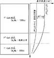
而且,当使用相同流量的Cp2Mg掺杂源或者通过顺序改变Cp2Mg的流量来生长具有0.1~0.5μm厚度范围的Mg掺杂p-GaN层时,合并从掺杂源中分离出的氢(H)气和NH3载气以在p-GaN层109中形成Mg-H络合物,其显示出大于约106Ω的高电阻绝缘特性。因此,为了在有源层107中的空穴和电子的再结合过程期间发射光,基本上需要活化过程以破坏Mg-H络合物的键。由于Mg掺杂p-GaN层109具有高电阻,因此其在没有任何改变的情况下无法使用。在600~800℃的温度范围和N2,N2/O2环境下通过退火过程来实施活化过程。然而,由于存在于p-GaN层109中的Mg具有低活化效率,因此其与用作第一电极接触层的n-GaN层105相比具有相对高的电阻值。在实际情况下,在活化过程之后,p-GaN层109中的Mg原子浓度在1019/cm3~1020/cm3的范围内,并且对纯载流子电导率有贡献的空穴载流子浓度在1017/cm3~1018/cm3的范围内,这相当于最大103倍的差异。另据报道空穴迁移率为10cm2/vsec,这是非常低的值。图2是示出传统的Mg掺杂p-GaN层的截面结构和在实施活化过程之后Mg掺杂p-GaN层内部的Mg分布曲线。参照图2,可以看出Mg原子浓度和空穴载流子浓度显示出最大103倍的差异。Also, when growing a Mg-doped p-GaN layer having a thickness ranging from 0.1 to 0.5 μm using the same flow rate of the Cp2 Mg doping source or by sequentially changing the flow rate of Cp2 Mg, the combined Hydrogen (H) gas and NH3 carrier gas to form a Mg-H complex in the p-
同时,在没有完全活化的情况下,p-GaN层109中残留的Mg原子浓度引起许多问题。例如,由有源层向表面发射的光被捕获从而降低光功率,或者当施加高电流时由于相对高的电阻值而产生热,使得发光器件的使用寿命被缩短,从而对可靠性产生致命的影响。具体而言,在使用倒装晶片技术的大尺寸/高功率的1mm×1mm发光器件的情况下,由于施加远高于20mA常规电流的350mA电流,所以在结表面产生高于100℃的结温度,其对器件的可靠性具有致命的影响并使将来的产品应用受限制。由于残留在用作第二电极接触层的p-GaN层109中的Mg原子浓度没有被活化为载流子而引起的电阻组分增加和由于电阻组分增加而引起的粗糙表面特性,因而导致大量生热。Meanwhile, the concentration of Mg atoms remaining in the p-
而且,在常规p-/n-结型发光器件中,用作第一电极接触层的n-GaN层105可以容易地将空穴浓度控制在5~6×1018/cm3的范围内并且控制在临界厚度内,所述临界厚度确保结晶度与随SiH4或Si2H6的流量增加而增加的硅掺杂浓度成比例,同时在用作第二电极接触层的p-GaN层109内,主要起载流子作用的空穴浓度被限制在1~9×1017/cm3的范围内,尽管Cp2Mg的流量增加并且掺杂大于最大值约1020/cm3的Mg原子。为此,传统的发光器件被制成具有不对称掺杂分布的p-/n-结型结构。Also, in conventional p-/n-junction light emitting devices, the n-
如上所述,用作第二电极接触层的p-GaN层109的低载流子浓度和高电阻组分导致发光效率降低。As described above, the low carrier concentration and high resistance composition of the p-
为了解决以上问题,已经提出了通过采用具有良好透射性和低接触电阻的Ni/Au TM(透明薄金属)来增加光功率的传统方法。然而,当应用于大尺寸/高功率的发光器件时,传统方法严重地影响器件的可靠性。在使用GaN半导体的发光器件中,这种问题仍悬而未决。To solve the above problems, a conventional method to increase optical power by adopting Ni/Au TM (transparent thin metal) with good transmittance and low contact resistance has been proposed. However, when applied to large-size/high-power light-emitting devices, conventional methods seriously affect device reliability. In light emitting devices using GaN semiconductors, such problems remain unsolved.
发明内容Contents of the invention
技术问题technical problem
本发明提供一种可以提高构成氮化物半导体发光器件的p-GaN层性能的氮化物半导体发光器件及其制造方法。The present invention provides a nitride semiconductor light emitting device capable of improving the performance of a p-GaN layer constituting the nitride semiconductor light emitting device and a manufacturing method thereof.
而且,本发明提供一种可以提高光功率和可靠性的氮化物半导体发光器件及其制造方法。Also, the present invention provides a nitride semiconductor light emitting device and a manufacturing method thereof that can improve optical power and reliability.
另外,本发明提供一种的氮化物半导体发光器件及其制造方法,该氮化物半导体发光器件可以克服由用作第二电极接触层的Mg掺杂p-GaN层的的低载流子浓度和迁移率以及在p-GaN层中保持完全未活化的Mg原子浓度的高电阻组分(包括Mg-H络合物)所引起的各种问题,并提高光功率和可靠性。In addition, the present invention provides a nitride semiconductor light emitting device and a manufacturing method thereof, which can overcome the low carrier concentration and the Mobility and various problems caused by high resistance components (including Mg-H complexes) that maintain a completely unactivated concentration of Mg atoms in the p-GaN layer, and improve optical power and reliability.
技术方案Technical solutions
提供一种氮化物半导体发光器件,包括:第一氮化物半导体层;形成在所述第一氮化物半导体层上方的有源层;和形成在所述有源层上方的δ掺杂第二氮化物半导体层。Provided is a nitride semiconductor light emitting device, comprising: a first nitride semiconductor layer; an active layer formed over the first nitride semiconductor layer; and a delta-doped second nitrogen oxide formed over the active layer compound semiconductor layer.
在本发明的另一个方面,提供一种氮化物半导体发光器件,包括:缓冲层;形成在所述缓冲层上方的第一氮化物半导体层;形成在所述第一氮化物半导体层上方的第一电极接触层;形成在所述第一氮化物半导体层上方的由阱层和势垒层组成的单量子阱结构或多量子阱结构的有源层;和形成在所述有源层上方的δ掺杂第二氮化物半导体层。In another aspect of the present invention, there is provided a nitride semiconductor light emitting device, comprising: a buffer layer; a first nitride semiconductor layer formed above the buffer layer; a first nitride semiconductor layer formed above the first nitride semiconductor layer. An electrode contact layer; an active layer of a single quantum well structure or a multi-quantum well structure formed on the first nitride semiconductor layer and formed on the first nitride semiconductor layer; and an active layer formed on the active layer delta-doped the second nitride semiconductor layer.
在本发明的另一个方面,提供一种制造氮化物半导体发光器件的方法,所述方法包括:在衬底上方形成缓冲层;在所述缓冲层上方形成第一氮化物半导体层;在所述第一氮化物半导体层上方形成有源层;和在所述有源层上方形成δ掺杂第二氮化物半导体层。In another aspect of the present invention, there is provided a method of manufacturing a nitride semiconductor light emitting device, the method comprising: forming a buffer layer over a substrate; forming a first nitride semiconductor layer over the buffer layer; An active layer is formed over the first nitride semiconductor layer; and a delta-doped second nitride semiconductor layer is formed over the active layer.
本发明还涉及以下技术方案。The present invention also relates to the following technical solutions.
1.一种氮化物半导体发光器件,包括:1. A nitride semiconductor light emitting device, comprising:
第一氮化物半导体层;a first nitride semiconductor layer;
形成在所述第一氮化物半导体层上方的有源层;和an active layer formed over the first nitride semiconductor layer; and
形成在所述有源层上方的δ掺杂第二氮化物半导体层。A delta-doped second nitride semiconductor layer is formed over the active layer.
2.根据技术方案1的氮化物半导体发光器件,还包括形成在所述δ掺杂第二氮化物半导体层上方的第三氮化物半导体层。2. The nitride semiconductor light emitting device according to technical solution 1, further comprising a third nitride semiconductor layer formed above the δ-doped second nitride semiconductor layer.
3.根据技术方案2的氮化物半导体发光器件,其中所述第三氮化物半导体层由具有铟含量逐渐变化的SG(超梯度)结构的n-InGaN层或n-InGaN/InGaN超晶格结构层构成。3. The nitride semiconductor light-emitting device according to technical solution 2, wherein the third nitride semiconductor layer is made of an n-InGaN layer or an n-InGaN/InGaN superlattice structure with a SG (super gradient) structure with a gradually changing indium content layer composition.
4.根据技术方案2的氮化物半导体发光器件,还包括形成在所述第三氮化物半导体层和所述δ掺杂第二氮化物半导体层之间的Si-掺杂GaN层。4. The nitride semiconductor light emitting device according to technical solution 2, further comprising a Si-doped GaN layer formed between the third nitride semiconductor layer and the delta-doped second nitride semiconductor layer.
5.根据技术方案2的氮化物半导体发光器件,还包括形成在所述第三氮化物半导体层上方的透明电极。5. The nitride semiconductor light emitting device according to technical solution 2, further comprising a transparent electrode formed over the third nitride semiconductor layer.
6.根据技术方案5的氮化物半导体发光器件,其中所述透明电极由选自ITO、IZO(In-ZnO)、GZO(Ga-ZnO)、AZO(Al-ZnO)、AGZO(Al-Ga ZnO)、IGZO(In-Ga ZnO)、IrOx、RuOx、RuOx/ITO、Ni/IrOx/Au、和Ni/IrOx/Au/ITO中的一种形成。6. The nitride semiconductor light-emitting device according to technical scheme 5, wherein said transparent electrode is selected from ITO, IZO (In-ZnO), GZO (Ga-ZnO), AZO (Al-ZnO), AGZO (Al-Ga ZnO ), IGZO (In-Ga ZnO),IrOx ,RuOx ,RuOx /ITO, Ni/IrOx /Au, and Ni/IrOx /Au/ITO are formed.
7.根据技术方案1的氮化物半导体发光器件,还包括:7. The nitride semiconductor light emitting device according to technical solution 1, further comprising:
位于所述第一氮化物半导体层下方的缓冲层;和a buffer layer under the first nitride semiconductor layer; and
位于所述缓冲层下方的衬底。A substrate located below the buffer layer.
8.根据技术方案7的氮化物半导体发光器件,还包括位于所述缓冲层上方的应变控制层。8. The nitride semiconductor light emitting device according to technical solution 7, further comprising a strain control layer located above the buffer layer.
9.根据技术方案7的氮化物半导体发光器件,其中所述缓冲层具有选自AlInN/GaN叠层结构、InGaN/GaN超晶格结构、InxGa1-xN/GaN叠层结构和AlxInyGa1-(x+y)N/InxGa1-xN/GaN叠层结构的结构。9. The nitride semiconductor light-emitting device according to technical solution 7, wherein the buffer layer has a structure selected from AlInN/GaN stacked structure, InGaN/GaN superlattice structure, Inx Ga1-x N/GaN stacked structure and Al The structure of thex Iny Ga1-(x+y) N/Inx Ga1-x N/GaN laminated structure.
10.根据技术方案1的氮化物半导体发光器件,还包括形成在所述第一氮化物半导体层和所述有源层之间并且具有1~5%铟含量的低摩尔含铟氮化物层。10. The nitride semiconductor light emitting device according to technical solution 1, further comprising a low mole indium-containing nitride layer formed between the first nitride semiconductor layer and the active layer and having an indium content of 1˜5%.
11.根据技术方案1的氮化物半导体发光器件,其中所述δ掺杂第二氮化物半导体层生长为
12.根据技术方案1的氮化物半导体发光器件,其中所述δ掺杂第二氮化物半导体层在选自未掺杂GaN/δ掺杂p-GaN、未掺杂AlGaN/δ掺杂p-GaN、未掺杂InGaN/δ掺杂p-GaN、未掺杂GaN/未掺杂AlGaN覆盖层/δ掺杂p-GaN、和未掺杂InGaN/未掺杂AlGaN覆盖层/δ掺杂p-GaN结构中的一种结构中重复生长。12. The nitride semiconductor light emitting device according to technical solution 1, wherein the δ-doped second nitride semiconductor layer is selected from undoped GaN/δ-doped p-GaN, undoped AlGaN/δ-doped p- GaN, undoped InGaN/delta doped p-GaN, undoped GaN/undoped AlGaN cladding/delta doped p-GaN, and undoped InGaN/undoped AlGaN cladding/delta doped p - Repeated growth in one of the GaN structures.
13.根据技术方案1的氮化物半导体发光器件,其中所述δ掺杂第二氮化物半导体层形成为具有由掺杂剂量变化的层组成的至少一个周期,其中在所述δ掺杂第二氮化物半导体层中重复生长所述周期。13. The nitride semiconductor light emitting device according to technical solution 1, wherein the δ-doped second nitride semiconductor layer is formed to have at least one period consisting of layers with varying doping doses, wherein the δ-doped second The period of growth is repeated in the nitride semiconductor layer.
14.根据技术方案1的氮化物半导体发光器件,其中所述δ掺杂第二氮化物半导体层包含选自Mgδ掺杂GaN层,Mg-Alδ掺杂GaN层和Mg-Al-Inδ掺杂GaN层中的一种。14. The nitride semiconductor light-emitting device according to technical solution 1, wherein the δ-doped second nitride semiconductor layer comprises an Mgδ-doped GaN layer, a Mg-Alδ-doped GaN layer, and a Mg-Al-Inδ-doped GaN layer. one of the layers.
15.根据技术方案1的氮化物半导体发光器件,其中所述δ掺杂第二氮化物半导体层在一个周期中重复生长至少两次,所述一个周期选自未掺杂GaN层/δ掺杂p-GaN层、未掺杂AlGaN层/δ掺杂p-GaN层、未掺杂InGaN层/δ掺杂p-GaN层、未掺杂GaN层/未掺杂AlGaN覆盖层/δ掺杂p-GaN层、和未掺杂InGaN层/未掺杂AlGaN覆盖层/δ掺杂p-GaN层结构中的一种,使得构成所述一个周期的选定层具有不同的厚度。15. The nitride semiconductor light-emitting device according to technical solution 1, wherein the δ-doped second nitride semiconductor layer is repeatedly grown at least twice in one cycle, and the one cycle is selected from undoped GaN layer/δ-doped p-GaN layer, undoped AlGaN layer/δ-doped p-GaN layer, undoped InGaN layer/δ-doped p-GaN layer, undoped GaN layer/undoped AlGaN capping layer/δ-doped p - one of a GaN layer, and an undoped InGaN layer/undoped AlGaN cladding layer/delta doped p-GaN layer structure such that selected layers constituting said one period have different thicknesses.
16.根据技术方案15的氮化物半导体发光器件,其中所述未掺杂AlGaN层生长为
17.根据技术方案15的氮化物半导体发光器件,其中所述未掺杂InGaN层生长为
18.根据技术方案15的氮化物半导体发光器件,其中所述未掺杂AlGaN覆盖层生长为的厚度并具有0.01~0.02的Al组成。18. The nitride semiconductor light emitting device according to technical solution 15, wherein the undoped AlGaN capping layer is grown as thickness and has an Al composition of 0.01 to 0.02.
19.根据技术方案1的氮化物半导体发光器件,其中所述第一氮化物半导体层是通过在1~9×10¹⁹/cm3的掺杂浓度范围内和1~4μm的厚度范围内同时掺杂Si-In而形成的n-GaN层。19. The nitride semiconductor light-emitting device according to technical solution 1, wherein the first nitride semiconductor layer is simultaneously doped in a doping concentration range of 1 to 9×10¹⁹ /cm3 and in a thickness range of 1 to 4 μm. n-GaN layer formed by doping Si-In.
20.根据技术方案1的氮化物半导体发光器件,其中所述第一氮化物半导体层通过使一个周期中的未掺杂AlGaN/掺杂GaN超晶格结构重复生长至少两次而形成为总厚度小于2μm。20. The nitride semiconductor light emitting device according to technical solution 1, wherein the first nitride semiconductor layer is formed to a total thickness by repeatedly growing the undoped AlGaN/doped GaN superlattice structure in one cycle at least twice less than 2μm.
21.根据技术方案20的氮化物半导体发光器件,其中所述未掺杂AlGaN层形成为
22.一种氮化物半导体发光器件,包括:22. A nitride semiconductor light emitting device, comprising:
缓冲层;The buffer layer;
形成在所述缓冲层上方的第一氮化物半导体层;a first nitride semiconductor layer formed over the buffer layer;
形成在所述第一氮化物半导体层上方的第一电极接触层;a first electrode contact layer formed over the first nitride semiconductor layer;
在所述第一氮化物半导体层上方形成为由阱层和势垒层组成的单量子阱结构或多量子阱结构的有源层;和forming an active layer of a single quantum well structure or a multiple quantum well structure consisting of a well layer and a barrier layer over the first nitride semiconductor layer; and
形成在所述有源层上方的Mg-δ掺杂第二氮化物半导体层。A Mg-δ doped second nitride semiconductor layer is formed over the active layer.
23.根据技术方案22的氮化物半导体发光器件,其中所述Mg-δ掺杂第二氮化物半导体层是第二电极接触层。23. The nitride semiconductor light emitting device according to technical solution 22, wherein the Mg-δ-doped second nitride semiconductor layer is a second electrode contact layer.
24.根据技术方案22的氮化物半导体发光器件,还包括形成在所述Mg-δ掺杂第二氮化物半导体层上方的n型第二电极接触层。24. The nitride semiconductor light emitting device according to technical solution 22, further comprising an n-type second electrode contact layer formed above the Mg-δ-doped second nitride semiconductor layer.
25.根据技术方案22的氮化物半导体发光器件,其中在所述阱层和所述势垒层之间进一步插入SiNx簇层。25. The nitride semiconductor light emitting device according to item 22, wherein aSiNx cluster layer is further inserted between the well layer and the barrier layer.
26.根据技术方案25的氮化物半导体发光器件,其中所述SiNx簇层用Si-δ掺杂方法生长。26. The nitride semiconductor light emitting device according to technical solution 25, wherein the SiNx cluster layer is grown by a Si-δ doping method.
27.一种制造氮化物半导体发光器件的方法,所述方法包括:27. A method of manufacturing a nitride semiconductor light emitting device, the method comprising:
在衬底上方形成缓冲层;forming a buffer layer over the substrate;
在所述缓冲层上方形成第一氮化物半导体层;forming a first nitride semiconductor layer over the buffer layer;
在所述第一氮化物半导体层上方形成有源层;和forming an active layer over the first nitride semiconductor layer; and
在所述有源层上方形成δ掺杂第二氮化物半导体层。A delta-doped second nitride semiconductor layer is formed over the active layer.
28.根据技术方案27的方法,其中所述缓冲层具有选自AlInN/GaN叠层结构、InGaN/GaN超晶格结构、InxGa1-xN/GaN叠层结构和AlxInyGa1-(x+y)N/InxGa1-xN/GaN叠层结构的结构。28. The method according to technical solution 27, wherein the buffer layer has a structure selected from AlInN/GaN stacked structure, InGaN/GaN superlattice structure, Inx Ga1-x N/GaN stacked structure and Alx Iny Ga The structure of the1-(x+y) N/Inx Ga1-x N/GaN stacked structure.
29.根据技术方案27的方法,在形成所述有源层之前,还包括形成具有1~5%的铟含量的低摩尔氮化物半导体层。29. The method according to technical solution 27, further comprising forming a low-mole nitride semiconductor layer having an indium content of 1-5% before forming the active layer.
30.根据技术方案27的方法,其中所述δ掺杂第二氮化物半导体层包括选自Mgδ掺杂GaN层、Mg-Alδ掺杂GaN层和Mg-Al-Inδ掺杂GaN层中的一种。30. The method according to technical solution 27, wherein the δ-doped second nitride semiconductor layer comprises one selected from a Mgδ-doped GaN layer, a Mg-Alδ-doped GaN layer, and a Mg-Al-Inδ-doped GaN layer kind.
31.根据技术方案27的方法,其中所述δ掺杂第二氮化物半导体层利用Cp2Mg或者DMZn MO(金属有机物)源生长为
32.根据技术方案27的方法,其中所述δ掺杂第二氮化物半导体层在选自未掺杂GaN层/δ掺杂p-GaN层、未掺杂AlGaN层/δ掺杂p-GaN层、未掺杂InGaN层/δ掺杂p-GaN层、未掺杂GaN层/未掺杂AlGaN覆盖层/δ掺杂p-GaN层、和未掺杂InGaN层/未掺杂AlGaN覆盖层/δ掺杂p-GaN层结构中的一种结构中重复生长至少一次。32. The method according to technical solution 27, wherein the δ-doped second nitride semiconductor layer is selected from undoped GaN layer/δ-doped p-GaN layer, undoped AlGaN layer/δ-doped p-GaN layer, undoped InGaN layer/δ-doped p-GaN layer, undoped GaN layer/undoped AlGaN cladding layer/δ-doped p-GaN layer, and undoped InGaN layer/undoped AlGaN cladding layer /δ-doped p-GaN layer structures are grown repeatedly at least once in one of the structures.
33.根据技术方案27的方法,其中所述δ掺杂第二氮化物半导体层形成为具有由掺杂剂量改变的层组成的至少一个周期,其中在所述δ掺杂第二氮化物半导体层中重复生长所述周期。33. The method according to technical solution 27, wherein the δ-doped second nitride semiconductor layer is formed to have at least one period consisting of layers whose dopant dose is changed, wherein the δ-doped second nitride semiconductor layer Repeat the growth cycle in .
34.根据技术方案27的方法,其中所述δ掺杂第二氮化物半导体层具有Cp2Mg和DMZn MO中的任何一种的掺杂源或TMAl和TMIn MO中的任何一种以及Cp2Mg和DMZn MO中的任何一种的掺杂源。34. The method according to technical scheme 27, wherein the δ-doped second nitride semiconductor layer has a dopant source of any one of Cp2 Mg and DMZn MO or any one of TMAl and TMIn MO and Cp2 Doping source for either Mg and DMZn MO.
35.根据技术方案27的方法,其中所述δ掺杂第二氮化物半导体层在一个周期中重复生长至少两次,所述一个周期选自未掺杂GaN层/δ掺杂p-GaN层、未掺杂AlGaN层/δ掺杂p-GaN层、未掺杂InGaN层/δ掺杂p-GaN层、未掺杂GaN层/未掺杂AlGaN覆盖层/δ掺杂p-GaN层、和未掺杂InGaN层/未掺杂AlGaN覆盖层/δ掺杂p-GaN层结构中的一种,使得构成所述一个周期的选定层具有不同的厚度。35. The method according to technical solution 27, wherein the δ-doped second nitride semiconductor layer is repeatedly grown at least twice in one cycle, and the one cycle is selected from an undoped GaN layer/δ-doped p-GaN layer , Undoped AlGaN layer/δ-doped p-GaN layer, Undoped InGaN layer/δ-doped p-GaN layer, Undoped GaN layer/Undoped AlGaN cladding layer/δ-doped p-GaN layer, and one of undoped InGaN layer/undoped AlGaN cladding layer/δ-doped p-GaN layer structure, so that the selected layers constituting the one period have different thicknesses.
36.根据技术方案35的方法,其中所述未掺杂AlGaN层生长为
37.根据技术方案35的方法,其中所述未掺杂InGaN层生长为

38.根据技术方案35的方法,其中所述未掺杂AlGaN覆盖层生长为
39.根据技术方案27的方法,还包括在所述第二氮化物半导体层上方形成第三氮化物半导体层。39. The method according to technical solution 27, further comprising forming a third nitride semiconductor layer over the second nitride semiconductor layer.
40.根据技术方案39的方法,其中所述第三氮化物半导体层由具有铟含量逐渐改变的SG(超梯度)结构的n-InGaN层或n-InGaN/InGaN超晶格层构成。40. The method according to technical item 39, wherein the third nitride semiconductor layer is composed of an n-InGaN layer or an n-InGaN/InGaN superlattice layer having a SG (super gradient) structure in which indium content gradually changes.
41.根据技术方案39的方法,还包括在所述第三氮化物半导体层和所述δ掺杂第二氮化物半导体层之间形成Si掺杂GaN层。41. The method according to technical solution 39, further comprising forming a Si-doped GaN layer between the third nitride semiconductor layer and the delta-doped second nitride semiconductor layer.
42.根据技术方案27的方法,还包括在形成所述缓冲层之后形成铟掺杂氮化物半导体层。42. The method according to technical solution 27, further comprising forming an indium-doped nitride semiconductor layer after forming the buffer layer.
43.根据技术方案27的方法,其中所述有源层提供为单量子阱结构或多量子阱结构,所述单量子阱结构由阱层/SiNx簇层/势垒层组成。43. The method according to technical solution 27, wherein the active layer is provided as a single quantum well structure or a multiple quantum well structure, and the single quantum well structure is composed of a well layer/SiNx cluster layer/barrier layer.
44.根据技术方案43的方法,其中所述SiNx簇层通过使用SiH4或SiH6作为掺杂源的Si-δ掺杂生长。44. The method according to technical solution 43, wherein the SiNx cluster layer is grown by Si-δ doping using SiH4 or SiH6 as a doping source.
有益效果Beneficial effect
根据本发明,提高构成氮化物半导体发光器件的p-GaN层的特性,提高氮化物半导体发光器件的光功率,改善光功率下降现象,并且提高抗ESD(静电放电)的可靠性。According to the present invention, the characteristics of the p-GaN layer constituting the nitride semiconductor light emitting device are improved, the optical power of the nitride semiconductor light emitting device is improved, the optical power drop phenomenon is improved, and the reliability against ESD (electrostatic discharge) is improved.
附图说明Description of drawings
通过附图将更容易理解本发明的实质。在附图中:The essence of the present invention will be more easily understood by the accompanying drawings. In the attached picture:
图1是示出常规氮化物半导体发光器件的叠层结构的示意图;1 is a schematic diagram showing a stacked structure of a conventional nitride semiconductor light emitting device;
图2是示出传统的Mg-掺杂p-GaN层的截面结构和在实施活化过程之后Mg掺杂p-GaN层内部的Mg分布的示意图;2 is a schematic view showing a cross-sectional structure of a conventional Mg-doped p-GaN layer and Mg distribution inside the Mg-doped p-GaN layer after performing an activation process;
图3是说明根据生长时间的Cp2Mgδ掺杂流量的示意图;FIG. 3 is a schematic diagram illustrating Cp2 Mg δ doping flux according to growth time;
图4是示出在Cp2Mgδ掺杂p-GaN晶体生长完成之后,在后续的活化过程之前和之后的Mg掺杂分布的视图;4 is a view showing Mg doping profiles before and after a subsequent activation process after completion of Cp2 Mg δ doped p-GaN crystal growth;
图5是示出在Cp2Mgδ掺杂p-GaN层的后续活化过程完成之后的电场分布的视图;5 is a view showing the electric field distribution after the completion of the subsequent activation process of theCp2Mgδ -doped p-GaN layer;
图6是示出根据本发明第一实施方案的氮化物半导体发光器件的叠层结构的示意图;和6 is a schematic diagram showing a stacked structure of a nitride semiconductor light emitting device according to a first embodiment of the present invention; and
图7是示出根据本发明第二实施方案的氮化物半导体发光器件的叠层结构的示意图。Fig. 7 is a schematic diagram showing a stacked structure of a nitride semiconductor light emitting device according to a second embodiment of the present invention.
具体实施方式Detailed ways
在下文中,将参照附图描述根据本发明实质的实施方案。Hereinafter, embodiments according to the essence of the present invention will be described with reference to the accompanying drawings.
本发明的特征在于氮化物半导体的制造方法,实施Cp2Mgδ掺杂过程以生长p-GaN层,将参照图3至图5描述Cp2Mgδ掺杂过程。The present invention is characterized by a method of manufacturing a nitride semiconductor, a Cp2 Mg δ doping process is performed to grow a p-GaN layer, and the Cp2 Mg δ doping process will be described with reference to FIGS. 3 to 5 .
图3是说明根据生长时间的Cp2Mgδ掺杂流量的示意图。FIG. 3 is a schematic diagram illustrating Cp2 Mg δ doping flux according to growth time.
参照图3,在生长发光有源层之后,生长小于

在生长Mg-δ掺杂GaN层时,可以改变构成一个周期的未掺杂GaN层和δ掺杂GaN层中的每一个的厚度。并且,在重复生长未掺杂GaN层/δ掺杂GaN层的一个周期时,可以改变每一周期的用量。同时,可以在
图4是示出在Cp2Mgδ掺杂p-GaN的晶体生长完成之后,在后续活化过程之前和之后的Mg掺杂分布的视图。FIG. 4 is a view showing Mg doping profiles before and after a subsequent activation process after the crystal growth of Cp2 Mg δ-doped p-GaN is completed.
参照图4,当在后续活化过程之前在恒定周期重复相同量的Cp2Mgδ掺杂时,可以在未掺杂GaN层之间的边界处获得具有陡峭的Mg掺杂分布曲线的δ掺杂GaN层。此后,当实施后续活化过程时,Mg扩散到两侧未掺杂GaN层内,以便获得宽的Mg掺杂分布。通过以上的后续活化过程,p-GaN层整体上具有均匀的Mg掺杂分布。Referring to Figure 4, when the same amount of Cp2 Mg δ doping is repeated at a constant period before the subsequent activation process, δ-doped GaN with a steep Mg doping profile can be obtained at the boundary between undoped GaN layers layer. Thereafter, when a subsequent activation process is performed, Mg diffuses into the undoped GaN layer on both sides, so as to obtain a broad Mg doping distribution. Through the above subsequent activation process, the p-GaN layer as a whole has a uniform Mg doping distribution.
通常,当向未掺杂GaN层施加正向偏压时,可以看到工作电压增加。在本发明中,可以通过控制Cp2Mgδ掺杂p-GaN层的厚度和未掺杂GaN层的厚度将工作电压有效地降低至小于3.5V(20mA),以增加发光器件的光功率。Typically, an increase in operating voltage is seen when a forward bias is applied to the undoped GaN layer. In the present invention, the operating voltage can be effectively reduced to less than 3.5V (20mA) by controlling the thickness of the Cp2 Mgδ-doped p-GaN layer and the thickness of the undoped GaN layer, so as to increase the optical power of the light-emitting device.
图5是示出在Cp2Mgδ掺杂p-GaN层的后续活化过程完成之后的电场分布的视图。FIG. 5 is a view showing the electric field distribution after the completion of the subsequent activation process of the Cp2 Mg δ doped p-GaN layer.
参照图5,可以看到,在周期性重复的Cp2Mgδ掺杂区内空穴载流子浓度分布是相对高的。因此,在Cp2Mgδ掺杂区域内,电势增加,以形成电场掺杂。因此,如在HEMT结构中利用能带差(AlGaN/GaN结)用作高速开关器件的2 DEG(二维电子阱层)一样,可以形成势阱,从而均匀和有效地控制空穴的流动,以及同样有效地控制电子的二维流动。总之,可见通过势阱能增加空穴注入率。Referring to FIG. 5 , it can be seen that the hole carrier concentration distribution is relatively high in the periodically repeated Cp2 Mg δ doped regions. Therefore, in the Cp2 Mgδ doped region, the potential increases to form electric field doping. Therefore, like 2 DEG (two-dimensional electron well layer) used as a high-speed switching device in a HEMT structure utilizing a band difference (AlGaN/GaN junction), a potential well can be formed to uniformly and efficiently control the flow of holes, and equally effectively control the two-dimensional flow of electrons. In conclusion, it can be seen that the hole injection rate can be increased through the potential well.
如从上面描述所看到的,通过传统技术生长的p-GaN层的问题在于,当施加正向偏压时,其高电阻组分急剧降低与从电极接触表面到其上表面的距离成反比的电流,同时在本发明中,势阱层可以更有效地增加电流密度以提高发光器件的光功率。As can be seen from the above description, the problem with p-GaN layers grown by conventional techniques is that, when a forward bias is applied, its high-resistance components drop sharply inversely proportional to the distance from the electrode contact surface to its upper surface At the same time, in the present invention, the potential well layer can increase the current density more effectively to increase the optical power of the light emitting device.
而且,通过Cp2Mgδ掺杂,由于掺杂元素以相对非常小的量被均匀地、重复地和周期性地掺杂,然后优化并实施用于p-GaN层的活化过程,因此可以降低其中存在的Mg、Mg-H络合物等的原子浓度,以尽可能地抑制电阻组分。换句话说,本发明增加完全贡献于电子电导率的空穴载流子浓度,从而增加其与电子再结合的概率,并且最终有效地增加光功率。因此,本发明提供一种可以减少电阻组分从而提高发光器件可靠性的高水平晶体生长技术。Moreover, by Cp2 Mgδ doping, since the doping element is uniformly, repeatedly and periodically doped in a relatively very small amount, and then the activation process for the p-GaN layer is optimized and implemented, it is possible to reduce the The atomic concentration of existing Mg, Mg-H complex, etc., to suppress the resistance component as much as possible. In other words, the present invention increases the concentration of hole carriers that fully contribute to electron conductivity, thereby increasing their probability of recombination with electrons, and ultimately effectively increasing optical power. Therefore, the present invention provides a high-level crystal growth technique that can reduce resistive components to improve reliability of a light emitting device.
在下文中,将详细描述根据本发明的氮化物半导体发光器件的实施方案。Hereinafter, embodiments of the nitride semiconductor light emitting device according to the present invention will be described in detail.
图6是示出根据本发明第一实施方案的氮化物半导体发光器件的叠层结构的示意图。Fig. 6 is a schematic diagram showing a stacked structure of a nitride semiconductor light emitting device according to a first embodiment of the present invention.
参照图6,根据本实施方案的氮化物半导体发光器件包括衬底401、缓冲层403、In掺杂GaN层405、n-GaN层407、低摩尔In掺杂GaN层或低摩尔InGaN层409、有源层411和Mg-δ掺杂p-GaN层413。已经参照图3至图5详细地描述了Mgδ掺杂p-GaN层413。6, the nitride semiconductor light emitting device according to this embodiment includes a
在下文中,将更详细地描述制造根据第一实施方案的氮化物半导体发光器件的方法。Hereinafter, a method of manufacturing the nitride semiconductor light emitting device according to the first embodiment will be described in more detail.
首先,在本实施方案中,在高温下仅将H2载气供应至蓝宝石衬底401上,以清洗蓝宝石衬底401。此后,在将生长温度降低至540℃的步骤中,供应NH3源气,以实施蓝宝石衬底401的氮化(nitridation),例如持续7分钟。First, in the present embodiment, only H2 carrier gas is supplied onto the
此后,使具有第一AlInN/第一GaN/第二AlInN/第二GaN结构的缓冲层403生长至约
此后,将生长温度降低至1050℃,然后在同样的生长温度下将硅和铟共掺杂n-GaN层407生长至2μm厚度。使用n-GaN层407作为第一电极层。Thereafter, the growth temperature was lowered to 1050° C., and then the silicon and indium co-doped n-
而且,为了调节有源层411的应变,在750℃下,使具有5%铟含量的低摩尔In掺杂GaN层或低摩尔InGaN层409(波长:480nm)生长至
此后,在相同的生长温度下,生长具有未掺杂InGaN/InGaN结构的单量子阱(SQW)的有源层411。在生长的有源层411中,势垒层具有小于5%的铟含量和约的厚度。此时,有源层411可以形成为多量子阱层。Thereafter, at the same growth temperature, an
此后,再次将生长温度升高至1000℃,将总厚度固定至0.1μm,也固定TMGa的流量,并且仅Cp2Mg的流量从0cc至1000cc被接通/切断,由此完成δ掺杂过程。为了有效地实施Cp2Mgδ掺杂,在生长发光有源层411后,首先将未掺杂GaN层生长为

在通过上述方法制成氮化物半导体发光器件后,利用ICP蚀刻装置实施台面蚀刻(mesa etching),并将氮化物半导体发光器件制成330μm×205μm的尺寸。分析并观察制成的氮化物半导体发光器件的电性能变化以检验其性能。结果,在正向偏压中的工作电压(20mA)低于3.4V,这与传统技术的值相同,但光功率增加50~100%。After the nitride semiconductor light emitting device was fabricated by the above method, mesa etching was performed using an ICP etching device, and the nitride semiconductor light emitting device was fabricated into a size of 330 μm×205 μm. Analyzing and observing the change of electrical properties of the manufactured nitride semiconductor light-emitting device to verify its performance. As a result, the operating voltage (20mA) in the forward bias is lower than 3.4V, which is the same value as the conventional technology, but the optical power is increased by 50-100%.
光功率增加的原因在于进入到形成在发光有源层的表面的“V”凹坑缺陷中的内部扩散被抑制,以及通过低于传统技术的Mg掺杂分布而降低在后续活化过程之后残留在所述层内的Mg原子(包括Mg-H络合物)的绝对量,但是对电子电导率有贡献的空穴载流子浓度增加。The reason for the increase in optical power is that the internal diffusion into the "V" pit defects formed on the surface of the light-emitting active layer is suppressed, and the Mg doping profile lower than that of the conventional technology is reduced by the Mg doping profile remaining after the subsequent activation process. The absolute amount of Mg atoms (including Mg-H complexes) within the layer, but the concentration of hole carriers that contribute to electronic conductivity increases.
图7示出根据本发明第二实施方案的氮化物半导体发光器件。Fig. 7 shows a nitride semiconductor light emitting device according to a second embodiment of the present invention.
参照图7,根据本发明第二实施方案的氮化物半导体发光器件包括衬底401、缓冲层403、In掺杂GaN层405、n-GaN层407、低摩尔In掺杂GaN层或低摩尔InGaN层409、有源层411、Mg-δ掺杂p-GaN层413和n-InGaN层515。Referring to FIG. 7, a nitride semiconductor light emitting device according to a second embodiment of the present invention includes a
与第一实施方案相比,上面的第二实施方案具有的区别在于,氮化物半导体发光器件还包括n-InGaN层515,因此,将仅额外描述n-InGaN层515,而其它元件的描述将参考第一实施方案。Compared with the first embodiment, the above second embodiment has a difference in that the nitride semiconductor light emitting device further includes an n-InGaN layer 515, therefore, only the n-InGaN layer 515 will be additionally described, and descriptions of other elements will be Reference is made to the first embodiment.
为了制造n-/p-/n-结型结构的发光器件,除了p-/n-结型结构的发光器件外,本发明的第二实施方案还生长Mg-δ掺杂p-GaN层416,然后生长n-InGaN层515,以用作第二电极接触层。In order to manufacture light-emitting devices with n-/p-/n-junction structure, in addition to the light-emitting devices with p-/n-junction structure, the second embodiment of the present invention also grows a Mg-δ doped p-GaN layer 416 , and then grow an n-InGaN layer 515 to serve as a second electrode contact layer.
在低至800℃的生长温度下,在NH3源气和N2载气的混合气体气氛下将用作第二电极接触层的n-InGaN层515生长至
发明模式invention model
除了上述实施方案之外,可以基于相同的实质提供多个其它实施例。In addition to the above-described embodiments, various other embodiments can be provided based on the same essence.
首先,可以在n-InGaN层515上进一步形成透明电极。该透明电极可以由选自ITO、IZO(In-ZnO)、GZO(Ga-ZnO)、AZO(Al-ZnO)、AGZO(Al-Ga ZnO)、IGZO(In-Ga ZnO)、IrOx、RuOx、RuOx/ITO、Ni/IrOx/Au、和Ni/IrOx/Au/ITO中的一种形成。First, a transparent electrode may be further formed on the n-InGaN layer 515 . The transparent electrode can be selected from ITO, IZO (In-ZnO), GZO (Ga-ZnO), AZO (Al-ZnO), AGZO (Al-Ga ZnO), IGZO (In-Ga ZnO), IrOx , RuOx ,RuOx /ITO, Ni/IrOx /Au, and Ni/IrOx /Au/ITO are formed.
并且,当第二实施方案说明n-InGaN层515形成为第二电极接触层时,n-InGaN/InGaN超晶格结构可以形成为第二电极接触层。作为替代方案,可以在n-InGaN/InGaN超晶格层和Mgδ掺杂p-GaN层413之间进一步形成Si掺杂GaN层。Also, when the second embodiment describes that the n-InGaN layer 515 is formed as the second electrode contact layer, an n-InGaN/InGaN superlattice structure may be formed as the second electrode contact layer. Alternatively, a Si-doped GaN layer may be further formed between the n-InGaN/InGaN superlattice layer and the Mgδ-doped p-
此外,第一和第二实施方案说明Mg在δ掺杂过程中被δ掺杂。然而,尽管过程类似,但是Mg-Al,Mg-Al-In等以及Mg可以被δ掺杂。此时,可以使用TMAl,TMInMO(金属有机物)作为掺杂源。Furthermore, the first and second embodiments illustrate that Mg is delta-doped during the delta doping process. However, although the process is similar, Mg-Al, Mg-Al-In etc. as well as Mg can be delta-doped. At this time, TMAl, TMInMO (metal organic compound) can be used as a dopant source.
此外,δ掺杂p-GaN层可以形成为具有由未掺杂AlGaN/δ掺杂p-GaN结构组成的一个周期,构成该一个周期的两层可以重复生长至少两次,未掺杂AlGaN层在
此外,δ掺杂p-GaN层可以形成为具有由未掺杂InGaN/δ掺杂p-GaN结构组成的一个周期,构成该一个周期的两层可以重复生长至少两次,未掺杂InGaN层在
而且,δ掺杂p-GaN层可以形成为具有由未掺杂GaN/未掺杂AlGaN覆盖层/δ掺杂p-GaN结构组成的一个周期,构成该一个周期的三层可以重复生长至少两次,未掺杂AlGaN覆盖层在
此外,δ掺杂p-GaN层可以形成为具有由未掺杂InGaN/未掺杂AlGaN覆盖层/δ掺杂p-GaN结构组成的一个周期,构成该一个周期的三层可以重复生长至少两次,未掺杂AlGaN覆盖层在
而且,在第一和第二实施方案中,用作第一电极接触层的n-GaN层可以是由Si和In共掺杂形成的n-GaN层,并且可以形成为1~9×10¹⁹/cm3的掺杂浓度和1~4μm的厚度范围。Also, in the first and second embodiments, the n-GaN layer used as the first electrode contact layer may be an n-GaN layer formed by Si and In co-doping, and may be formed to be 1˜9×10¹⁹ /cm3 doping concentration and a thickness range of 1 to 4 μm.
此外,第一电极接触层可以形成为具有由未掺杂AlGaN/掺杂GaN超晶格结构组成的一个周期,构成该一个周期的两层可以重复生长至少两次,具有1~2μm的总厚度和0.05~0.3的Al组成。掺杂GaN层形成为
此外,有源层可以制成由阱层/SiNx簇层/势垒层组成的单量子阱结构或多量子阱结构,而且SiNx簇层可以通过Si-δ掺杂方法生长。可以利用单独的SiH4掺杂源或SiH6通过Si-δ掺杂来生长SiNx簇层。In addition, the active layer can be made into a single quantum well structure or a multi-quantum well structure composed of well layer/SiNx cluster layer/barrier layer, and the SiNx cluster layer can be grown by Si-δ doping method. TheSiNx cluster layer can be grown with a separate SiH4 doping source or SiH6 by Si-δ doping.
工业适用性Industrial applicability
根据本发明提供的氮化物半导体发光器件及其制造方法,提高光功率,改善功率下降现象,并且提高抗ESD(静电放电)的可靠性。According to the nitride semiconductor light-emitting device and the manufacturing method thereof provided by the present invention, the light power is increased, the power drop phenomenon is improved, and the reliability against ESD (electrostatic discharge) is improved.
而且,本发明可以应用于需要高光功率和高可靠性的照明装置。Also, the present invention can be applied to lighting devices that require high optical power and high reliability.
Claims (14)
Translated fromChinese


Applications Claiming Priority (3)
| Application Number | Priority Date | Filing Date | Title |
|---|---|---|---|
| KR10-2004-0111087 | 2004-12-23 | ||
| KR1020040111087 | 2004-12-23 | ||
| KR1020040111087AKR100662191B1 (en) | 2004-12-23 | 2004-12-23 | Nitride semiconductor light emitting device and manufacturing method |
Related Parent Applications (1)
| Application Number | Title | Priority Date | Filing Date |
|---|---|---|---|
| CNB2005800409633ADivisionCN100555682C (en) | 2004-12-23 | 2005-12-05 | Nitride semiconductor light emitting device and method for manufacturing the same |
Publications (2)
| Publication Number | Publication Date |
|---|---|
| CN101577305A CN101577305A (en) | 2009-11-11 |
| CN101577305Btrue CN101577305B (en) | 2012-02-01 |
Family
ID=36601937
Family Applications (2)
| Application Number | Title | Priority Date | Filing Date |
|---|---|---|---|
| CN2009101430383AExpired - Fee RelatedCN101577305B (en) | 2004-12-23 | 2005-12-05 | Nitride semiconductor light emitting device and manufacturing method thereof |
| CNB2005800409633AExpired - Fee RelatedCN100555682C (en) | 2004-12-23 | 2005-12-05 | Nitride semiconductor light emitting device and method for manufacturing the same |
Family Applications After (1)
| Application Number | Title | Priority Date | Filing Date |
|---|---|---|---|
| CNB2005800409633AExpired - Fee RelatedCN100555682C (en) | 2004-12-23 | 2005-12-05 | Nitride semiconductor light emitting device and method for manufacturing the same |
Country Status (7)
| Country | Link |
|---|---|
| US (5) | US7791062B2 (en) |
| EP (3) | EP2306529A3 (en) |
| JP (2) | JP2008526014A (en) |
| KR (1) | KR100662191B1 (en) |
| CN (2) | CN101577305B (en) |
| DE (2) | DE202005021971U1 (en) |
| WO (1) | WO2006068376A1 (en) |
Families Citing this family (49)
| Publication number | Priority date | Publication date | Assignee | Title |
|---|---|---|---|---|
| KR100662191B1 (en)* | 2004-12-23 | 2006-12-27 | 엘지이노텍 주식회사 | Nitride semiconductor light emitting device and manufacturing method |
| KR100580751B1 (en) | 2004-12-23 | 2006-05-15 | 엘지이노텍 주식회사 | Nitride semiconductor light emitting device and manufacturing method |
| EP1883140B1 (en) | 2006-07-27 | 2013-02-27 | OSRAM Opto Semiconductors GmbH | LD or LED with superlattice clad layer and graded doping |
| EP1883141B1 (en) | 2006-07-27 | 2017-05-24 | OSRAM Opto Semiconductors GmbH | LD or LED with superlattice cladding layer |
| PL1883119T3 (en) | 2006-07-27 | 2016-04-29 | Osram Opto Semiconductors Gmbh | Semiconductor layer structure with overlay grid |
| JP4462251B2 (en)* | 2006-08-17 | 2010-05-12 | 日立電線株式会社 | III-V nitride semiconductor substrate and III-V nitride light emitting device |
| KR101438806B1 (en) | 2007-08-28 | 2014-09-12 | 엘지이노텍 주식회사 | Semiconductor light emitting device and manufacturing method thereof |
| JP2009177029A (en)* | 2008-01-25 | 2009-08-06 | Sumitomo Electric Ind Ltd | Method for manufacturing a semiconductor film |
| JP4640427B2 (en)* | 2008-03-14 | 2011-03-02 | ソニー株式会社 | GaN-based semiconductor light-emitting device, light-emitting device assembly, light-emitting device, method for manufacturing GaN-based semiconductor light-emitting device, driving method for GaN-based semiconductor light-emitting device, and image display device |
| DE102008056371A1 (en)* | 2008-11-07 | 2010-05-12 | Osram Opto Semiconductors Gmbh | Method for producing an optoelectronic semiconductor chip and optoelectronic semiconductor chip |
| KR101047691B1 (en)* | 2008-12-12 | 2011-07-08 | 엘지이노텍 주식회사 | Semiconductor light emitting device and manufacturing method thereof |
| KR101039982B1 (en)* | 2010-03-18 | 2011-06-09 | 엘지이노텍 주식회사 | Light emitting device and manufacturing method |
| US10134948B2 (en)* | 2011-02-25 | 2018-11-20 | Sensor Electronic Technology, Inc. | Light emitting diode with polarization control |
| JP5023230B1 (en) | 2011-05-16 | 2012-09-12 | 株式会社東芝 | Nitride semiconductor element, nitride semiconductor wafer, and method of manufacturing nitride semiconductor layer |
| JP5885942B2 (en)* | 2011-05-30 | 2016-03-16 | シャープ株式会社 | Nitride semiconductor light emitting device and manufacturing method thereof |
| CN102881784B (en)* | 2011-07-14 | 2016-02-03 | 比亚迪股份有限公司 | The p-type GaN/AlGaN structure that C δ adulterates, LED structure and preparation method |
| CN103178169B (en)* | 2011-12-22 | 2015-08-26 | 比亚迪股份有限公司 | A kind of LED and preparation method thereof |
| KR101881064B1 (en)* | 2012-03-05 | 2018-07-24 | 삼성전자주식회사 | Nitride Semiconductor light emitting device and manufacturing method of the same |
| JP6054620B2 (en) | 2012-03-29 | 2016-12-27 | トランスフォーム・ジャパン株式会社 | Compound semiconductor device and manufacturing method thereof |
| JP5337272B2 (en)* | 2012-04-16 | 2013-11-06 | 株式会社東芝 | Nitride semiconductor element, nitride semiconductor wafer, and method of manufacturing nitride semiconductor layer |
| KR101376976B1 (en)* | 2012-06-29 | 2014-03-21 | 인텔렉추얼디스커버리 주식회사 | Semiconductor light generating device |
| KR102035192B1 (en)* | 2013-03-21 | 2019-10-22 | 엘지이노텍 주식회사 | Light emitting device |
| DE102013104272A1 (en) | 2013-04-26 | 2014-10-30 | Osram Opto Semiconductors Gmbh | Optoelectronic component and method for its production |
| CN103367594B (en)* | 2013-07-26 | 2015-12-02 | 东南大学 | A kind of light-emitting diode and preparation method thereof |
| CN103489972A (en)* | 2013-09-24 | 2014-01-01 | 西安神光皓瑞光电科技有限公司 | LED structure resistant to electrostatic breakdown |
| CN103500702A (en)* | 2013-10-09 | 2014-01-08 | 西安神光皓瑞光电科技有限公司 | Low-diffusion and high-hole concentration P type GaN-based material growing method |
| CN103681986B (en)* | 2013-11-27 | 2016-02-10 | 江西圆融光电科技有限公司 | A kind of gallium nitride based LED epitaxial slice and preparation method thereof |
| US9224815B2 (en)* | 2014-01-03 | 2015-12-29 | Taiwan Semiconductor Manufacturing Company, Ltd. | Method of tuning doping concentration in III-V compound semiconductor through co-doping donor and acceptor impurities |
| KR102198693B1 (en) | 2014-01-15 | 2021-01-06 | 삼성전자주식회사 | Semiconductor light emitting device |
| CN103956413B (en)* | 2014-04-23 | 2017-04-12 | 湘能华磊光电股份有限公司 | LED epitaxial layer growing method and prepared LED epitaxial layer |
| JP6986349B2 (en)* | 2014-05-27 | 2021-12-22 | シランナ・ユー・ブイ・テクノロジーズ・プライベート・リミテッドSilanna Uv Technologies Pte Ltd | Electronic device with n-type superlattice and p-type superlattice |
| JP6817072B2 (en) | 2014-05-27 | 2021-01-20 | シランナ・ユー・ブイ・テクノロジーズ・プライベート・リミテッドSilanna Uv Technologies Pte Ltd | Optoelectronic device |
| JP6636459B2 (en) | 2014-05-27 | 2020-01-29 | シランナ・ユー・ブイ・テクノロジーズ・プライベート・リミテッドSilanna Uv Technologies Pte Ltd | Advanced electronic devices using semiconductor structures and superlattices |
| US11322643B2 (en) | 2014-05-27 | 2022-05-03 | Silanna UV Technologies Pte Ltd | Optoelectronic device |
| CN104091872B (en)* | 2014-07-30 | 2016-08-17 | 湘能华磊光电股份有限公司 | LED, growing method and the LED structure of Mg diffusion |
| KR102264671B1 (en) | 2014-09-30 | 2021-06-15 | 서울바이오시스 주식회사 | Vertical ultraviolet light emitting device |
| TWI581453B (en)* | 2014-12-23 | 2017-05-01 | 錼創科技股份有限公司 | Semiconductor light-emitting element |
| JP6380172B2 (en)* | 2015-03-06 | 2018-08-29 | 豊田合成株式会社 | Group III nitride semiconductor light emitting device and method for manufacturing the same |
| KR102604739B1 (en) | 2017-01-05 | 2023-11-22 | 삼성전자주식회사 | Semiconductor Light Emitting Device |
| DE102017119931A1 (en)* | 2017-08-30 | 2019-02-28 | Osram Opto Semiconductors Gmbh | Optoelectronic semiconductor component |
| CN113451458B (en)* | 2020-05-22 | 2022-04-01 | 重庆康佳光电技术研究院有限公司 | Superlattice layer, LED epitaxial structure, display device and manufacturing method thereof |
| KR102540198B1 (en) | 2020-05-22 | 2023-06-02 | 충칭 콘카 포토일렉트릭 테크놀로지 리서치 인스티튜트 컴퍼니 리미티드 | Superlattice layer, LED epitaxial structure, display device and manufacturing method thereof |
| CN112048710B (en)* | 2020-09-07 | 2023-09-19 | 湘能华磊光电股份有限公司 | LED epitaxial growth method for reducing blue shift of LED luminous wavelength |
| CN115050825A (en)* | 2021-03-09 | 2022-09-13 | 广西飓芯科技有限责任公司 | Preparation method of p-type III-V semiconductor material with low specific contact resistivity in ohmic contact with conductive electrode |
| KR20240019839A (en)* | 2021-07-15 | 2024-02-14 | 안후이 산안 옵토일렉트로닉스 컴퍼니 리미티드 | Semiconductor light-emitting devices and light-emitting devices |
| CN114388664B (en)* | 2021-12-29 | 2023-08-29 | 南昌大学 | A growth method for improving photoelectric conversion efficiency of GaN-based light-emitting devices |
| CN115172542A (en)* | 2022-02-22 | 2022-10-11 | 江西兆驰半导体有限公司 | LED epitaxial wafer, epitaxial growth method and LED chip |
| CN116130564B (en)* | 2023-03-09 | 2023-12-19 | 安徽格恩半导体有限公司 | Semiconductor light-emitting diode |
| CN118431366B (en)* | 2024-07-04 | 2024-09-20 | 江西兆驰半导体有限公司 | LED epitaxial wafer, preparation method thereof and LED |
Citations (3)
| Publication number | Priority date | Publication date | Assignee | Title |
|---|---|---|---|---|
| CN1265228A (en)* | 1997-07-25 | 2000-08-30 | 日亚化学工业株式会社 | Nitride semiconductor device |
| CN1413362A (en)* | 1998-09-16 | 2003-04-23 | 克里公司 | Vertical geometry InGaN light-emitting diode |
| CN1447447A (en)* | 2002-03-27 | 2003-10-08 | 联铨科技股份有限公司 | LED in III group nitride and its manufacturing methods |
Family Cites Families (31)
| Publication number | Priority date | Publication date | Assignee | Title |
|---|---|---|---|---|
| JP3605907B2 (en)* | 1994-10-28 | 2004-12-22 | 三菱化学株式会社 | Semiconductor device having contact resistance reduction layer |
| US6677619B1 (en)* | 1997-01-09 | 2004-01-13 | Nichia Chemical Industries, Ltd. | Nitride semiconductor device |
| CN1964094B (en)* | 1997-01-09 | 2012-03-14 | 日亚化学工业株式会社 | Nitride semiconductor device |
| JPH10294531A (en)* | 1997-02-21 | 1998-11-04 | Toshiba Corp | Nitride compound semiconductor light emitting device |
| JP4225594B2 (en)* | 1997-08-04 | 2009-02-18 | 三洋電機株式会社 | Gallium nitride compound semiconductor device |
| EP2273571A3 (en)* | 1998-03-12 | 2012-06-27 | Nichia Corporation | A nitride semiconductor device |
| US6657300B2 (en)* | 1998-06-05 | 2003-12-02 | Lumileds Lighting U.S., Llc | Formation of ohmic contacts in III-nitride light emitting devices |
| ES2194402T3 (en) | 1998-06-12 | 2003-11-16 | Hoffmann La Roche | DERIVATIVES OF DI - O TRIAZA-ESPIRO (4,5) DECANO .. |
| JP4149054B2 (en)* | 1998-11-27 | 2008-09-10 | シャープ株式会社 | Semiconductor device |
| KR100288851B1 (en)* | 1999-03-25 | 2001-04-16 | 조장연 | Method for making a III-Nitride semiconductor light-emitting device using delta-doping technique |
| CN1347581A (en)* | 1999-03-26 | 2002-05-01 | 松下电器产业株式会社 | Semiconductor structures having strain compensated layer and method of fabrication |
| KR100330228B1 (en)* | 1999-04-07 | 2002-03-25 | 조장연 | GaN-based Semiconductor Light Emitting Devices of Quantum Well Electronic Structures Resonating with Two-dimensional Electron Gas |
| JP3609661B2 (en)* | 1999-08-19 | 2005-01-12 | 株式会社東芝 | Semiconductor light emitting device |
| US6586762B2 (en)* | 2000-07-07 | 2003-07-01 | Nichia Corporation | Nitride semiconductor device with improved lifetime and high output power |
| WO2002023640A1 (en) | 2000-09-14 | 2002-03-21 | Optowell Co., Ltd. | Nitride compound semiconductor light emitting device having a tunnel junction structure and fabrication method thereof |
| KR100380536B1 (en) | 2000-09-14 | 2003-04-23 | 주식회사 옵토웰 | III-Nitride compound semiconductor light emitting device having a tunnel junction structure |
| KR100384598B1 (en)* | 2000-11-29 | 2003-05-22 | 주식회사 옵토웰 | Nitride compound semiconductor vertical-cavity surface-emitting laser |
| JP3453558B2 (en)* | 2000-12-25 | 2003-10-06 | 松下電器産業株式会社 | Nitride semiconductor device |
| TW488088B (en)* | 2001-01-19 | 2002-05-21 | South Epitaxy Corp | Light emitting diode structure |
| KR100889842B1 (en)* | 2001-07-04 | 2009-03-20 | 니치아 카가쿠 고교 가부시키가이샤 | Nitride Semiconductor Devices |
| TW550839B (en)* | 2001-07-25 | 2003-09-01 | Shinetsu Handotai Kk | Light emitting element and method for manufacturing thereof |
| US6833564B2 (en) | 2001-11-02 | 2004-12-21 | Lumileds Lighting U.S., Llc | Indium gallium nitride separate confinement heterostructure light emitting devices |
| US7919791B2 (en)* | 2002-03-25 | 2011-04-05 | Cree, Inc. | Doped group III-V nitride materials, and microelectronic devices and device precursor structures comprising same |
| KR100497890B1 (en)* | 2002-08-19 | 2005-06-29 | 엘지이노텍 주식회사 | Nitride semiconductor LED and fabrication method for thereof |
| KR100497127B1 (en)* | 2002-09-05 | 2005-06-28 | 삼성전기주식회사 | AlGaInN semiconductor LED device |
| US6921929B2 (en)* | 2003-06-27 | 2005-07-26 | Lockheed Martin Corporation | Light-emitting diode (LED) with amorphous fluoropolymer encapsulant and lens |
| WO2005050748A1 (en)* | 2003-11-19 | 2005-06-02 | Nichia Corporation | Semiconductor device and method for manufacturing same |
| JP4999278B2 (en) | 2004-02-24 | 2012-08-15 | 昭和電工株式会社 | Gallium nitride compound semiconductor light emitting device |
| KR100662191B1 (en)* | 2004-12-23 | 2006-12-27 | 엘지이노텍 주식회사 | Nitride semiconductor light emitting device and manufacturing method |
| JP3759746B2 (en) | 2005-04-08 | 2006-03-29 | シャープ株式会社 | Method for producing group III nitride compound semiconductor light emitting diode |
| JP2005252309A (en) | 2005-05-30 | 2005-09-15 | Toshiba Corp | Method for manufacturing gallium nitride based semiconductor light emitting device |
- 2004
- 2004-12-23KRKR1020040111087Apatent/KR100662191B1/ennot_activeExpired - Fee Related
- 2005
- 2005-12-05DEDE202005021971Upatent/DE202005021971U1/ennot_activeExpired - Lifetime
- 2005-12-05EPEP10191955.3Apatent/EP2306529A3/ennot_activeCeased
- 2005-12-05CNCN2009101430383Apatent/CN101577305B/ennot_activeExpired - Fee Related
- 2005-12-05EPEP10191954Apatent/EP2306528A3/ennot_activeCeased
- 2005-12-05DEDE202005021990Upatent/DE202005021990U1/ennot_activeExpired - Lifetime
- 2005-12-05EPEP05821284Apatent/EP1829120A4/ennot_activeWithdrawn
- 2005-12-05JPJP2007548057Apatent/JP2008526014A/enactivePending
- 2005-12-05CNCNB2005800409633Apatent/CN100555682C/ennot_activeExpired - Fee Related
- 2005-12-05WOPCT/KR2005/004120patent/WO2006068376A1/enactiveApplication Filing
- 2005-12-05USUS11/719,929patent/US7791062B2/enactiveActive
- 2010
- 2010-08-03USUS12/849,265patent/US8278646B2/enactiveActive
- 2012
- 2012-07-11JPJP2012155208Apatent/JP2012195616A/enactivePending
- 2012-08-14USUS13/585,451patent/US8674340B2/enactiveActive
- 2014
- 2014-03-09USUS14/201,883patent/US8969849B2/enactiveActive
- 2015
- 2015-01-23USUS14/604,133patent/US9190567B2/ennot_activeExpired - Fee Related
Patent Citations (3)
| Publication number | Priority date | Publication date | Assignee | Title |
|---|---|---|---|---|
| CN1265228A (en)* | 1997-07-25 | 2000-08-30 | 日亚化学工业株式会社 | Nitride semiconductor device |
| CN1413362A (en)* | 1998-09-16 | 2003-04-23 | 克里公司 | Vertical geometry InGaN light-emitting diode |
| CN1447447A (en)* | 2002-03-27 | 2003-10-08 | 联铨科技股份有限公司 | LED in III group nitride and its manufacturing methods |
Non-Patent Citations (1)
| Title |
|---|
| M. L. Nakarmi等.Enhanced p-type conduction in GaN and AlGaN by Mg-δ-doping.《APPLIED PHYSICS LETTERS》.2003,第82卷(第18期),* |
Also Published As
| Publication number | Publication date |
|---|---|
| EP2306529A2 (en) | 2011-04-06 |
| KR100662191B1 (en) | 2006-12-27 |
| US8278646B2 (en) | 2012-10-02 |
| CN100555682C (en) | 2009-10-28 |
| US7791062B2 (en) | 2010-09-07 |
| EP2306528A2 (en) | 2011-04-06 |
| US20150137071A1 (en) | 2015-05-21 |
| EP1829120A1 (en) | 2007-09-05 |
| DE202005021990U1 (en) | 2012-01-31 |
| US20120313109A1 (en) | 2012-12-13 |
| CN101577305A (en) | 2009-11-11 |
| WO2006068376A1 (en) | 2006-06-29 |
| US20090166606A1 (en) | 2009-07-02 |
| US8674340B2 (en) | 2014-03-18 |
| CN101069289A (en) | 2007-11-07 |
| US20140183449A1 (en) | 2014-07-03 |
| US8969849B2 (en) | 2015-03-03 |
| US20100289002A1 (en) | 2010-11-18 |
| JP2012195616A (en) | 2012-10-11 |
| EP1829120A4 (en) | 2010-06-02 |
| DE202005021971U1 (en) | 2011-11-11 |
| EP2306528A3 (en) | 2013-04-03 |
| EP2306529A3 (en) | 2013-04-10 |
| US9190567B2 (en) | 2015-11-17 |
| JP2008526014A (en) | 2008-07-17 |
| KR20060072446A (en) | 2006-06-28 |
Similar Documents
| Publication | Publication Date | Title |
|---|---|---|
| CN101577305B (en) | Nitride semiconductor light emitting device and manufacturing method thereof | |
| CN100466307C (en) | Nitride semiconductor light emitting device | |
| JP4966865B2 (en) | Nitride semiconductor light emitting device and manufacturing method thereof | |
| JP5048497B2 (en) | Nitride semiconductor light emitting device and manufacturing method thereof | |
| CN100568551C (en) | Nitride semiconductor light emitting device and method for manufacturing the same | |
| CN108550675A (en) | A kind of LED epitaxial slice and preparation method thereof | |
| CN108831974A (en) | A light-emitting diode epitaxial wafer and its manufacturing method | |
| CN108550669A (en) | Nitride semiconductor structure and semiconductor light emitting element | |
| CN108075019B (en) | Light emitting diode epitaxial wafer and preparation method thereof | |
| CN104952994A (en) | P-type LED structure of Al component gradual change type, and manufacturing method | |
| KR100593151B1 (en) | Nitride semiconductor light emitting device and manufacturing method | |
| CN101027792A (en) | Nitride semiconductor light emitting device and manufacturing method thereof | |
| CN107968138A (en) | A kind of iii-nitride light emitting devices | |
| JP2025026068A (en) | Light emitting element | |
| KR20070035660A (en) | Nitride semiconductor light emitting device manufacturing method | |
| KR20160014343A (en) | Light emitting device and lighting system |
Legal Events
| Date | Code | Title | Description |
|---|---|---|---|
| C06 | Publication | ||
| PB01 | Publication | ||
| C10 | Entry into substantive examination | ||
| SE01 | Entry into force of request for substantive examination | ||
| C14 | Grant of patent or utility model | ||
| GR01 | Patent grant | ||
| CF01 | Termination of patent right due to non-payment of annual fee | Granted publication date:20120201 Termination date:20191205 | |
| CF01 | Termination of patent right due to non-payment of annual fee |