CN101577256A - Semiconductor device and method of manufacturing the same - Google Patents
Semiconductor device and method of manufacturing the sameDownload PDFInfo
- Publication number
- CN101577256A CN101577256ACNA2009101298604ACN200910129860ACN101577256ACN 101577256 ACN101577256 ACN 101577256ACN A2009101298604 ACNA2009101298604 ACN A2009101298604ACN 200910129860 ACN200910129860 ACN 200910129860ACN 101577256 ACN101577256 ACN 101577256A
- Authority
- CN
- China
- Prior art keywords
- film
- substrate
- liquid crystal
- insulating film
- conductive film
- Prior art date
- Legal status (The legal status is an assumption and is not a legal conclusion. Google has not performed a legal analysis and makes no representation as to the accuracy of the status listed.)
- Granted
Links
- 239000004065semiconductorSubstances0.000titleclaimsabstractdescription146
- 238000004519manufacturing processMethods0.000titleclaimsabstractdescription42
- 229910000838Al alloyInorganic materials0.000claimsabstractdescription22
- 239000010408filmSubstances0.000claimsdescription633
- XLOMVQKBTHCTTD-UHFFFAOYSA-NZinc monoxideChemical compound[Zn]=OXLOMVQKBTHCTTD-UHFFFAOYSA-N0.000claimsdescription119
- 239000000758substrateSubstances0.000claimsdescription113
- 239000010410layerSubstances0.000claimsdescription90
- 239000011787zinc oxideSubstances0.000claimsdescription59
- 239000004973liquid crystal related substanceSubstances0.000claimsdescription38
- 239000000463materialSubstances0.000claimsdescription33
- 229910052751metalInorganic materials0.000claimsdescription24
- 239000002184metalSubstances0.000claimsdescription24
- 229910052782aluminiumInorganic materials0.000claimsdescription20
- 239000011159matrix materialSubstances0.000claimsdescription20
- 229920005989resinPolymers0.000claimsdescription18
- 239000011347resinSubstances0.000claimsdescription18
- XAGFODPZIPBFFR-UHFFFAOYSA-NaluminiumChemical compound[Al]XAGFODPZIPBFFR-UHFFFAOYSA-N0.000claimsdescription13
- 239000000203mixtureSubstances0.000claimsdescription13
- 239000010409thin filmSubstances0.000claimsdescription12
- 239000010936titaniumSubstances0.000claimsdescription12
- 230000015572biosynthetic processEffects0.000claimsdescription9
- RTAQQCXQSZGOHL-UHFFFAOYSA-NTitaniumChemical compound[Ti]RTAQQCXQSZGOHL-UHFFFAOYSA-N0.000claimsdescription5
- 229910052719titaniumInorganic materials0.000claimsdescription5
- 239000008393encapsulating agentSubstances0.000claims4
- XUIMIQQOPSSXEZ-UHFFFAOYSA-NSiliconChemical compound[Si]XUIMIQQOPSSXEZ-UHFFFAOYSA-N0.000abstractdescription48
- 229910052710siliconInorganic materials0.000abstractdescription48
- 239000010703siliconSubstances0.000abstractdescription48
- 229910052814silicon oxideInorganic materials0.000abstractdescription42
- VYPSYNLAJGMNEJ-UHFFFAOYSA-NSilicium dioxideChemical compoundO=[Si]=OVYPSYNLAJGMNEJ-UHFFFAOYSA-N0.000abstractdescription40
- 239000012535impuritySubstances0.000abstractdescription35
- 230000007547defectEffects0.000abstractdescription3
- 230000007257malfunctionEffects0.000abstract1
- 238000005530etchingMethods0.000description45
- 238000000034methodMethods0.000description36
- 239000000126substanceSubstances0.000description28
- 238000004544sputter depositionMethods0.000description27
- 239000003990capacitorSubstances0.000description23
- WGTYBPLFGIVFAS-UHFFFAOYSA-Mtetramethylammonium hydroxideChemical compound[OH-].C[N+](C)(C)CWGTYBPLFGIVFAS-UHFFFAOYSA-M0.000description20
- KRHYYFGTRYWZRS-UHFFFAOYSA-NFluoraneChemical compoundFKRHYYFGTRYWZRS-UHFFFAOYSA-N0.000description16
- IJGRMHOSHXDMSA-UHFFFAOYSA-NAtomic nitrogenChemical compoundN#NIJGRMHOSHXDMSA-UHFFFAOYSA-N0.000description13
- 229910052581Si3N4Inorganic materials0.000description13
- HQVNEWCFYHHQES-UHFFFAOYSA-Nsilicon nitrideChemical compoundN12[Si]34N5[Si]62N3[Si]51N64HQVNEWCFYHHQES-UHFFFAOYSA-N0.000description13
- 238000001039wet etchingMethods0.000description13
- 239000011521glassSubstances0.000description12
- 238000002347injectionMethods0.000description12
- 239000007924injectionSubstances0.000description12
- 229920002120photoresistant polymerPolymers0.000description12
- 238000005192partitionMethods0.000description11
- 238000001312dry etchingMethods0.000description10
- -1polyethylene terephthalatePolymers0.000description10
- 239000002356single layerSubstances0.000description10
- 229910001151AlNiInorganic materials0.000description9
- 239000002585baseSubstances0.000description9
- 238000002161passivationMethods0.000description9
- 239000000565sealantSubstances0.000description9
- 239000010949copperSubstances0.000description8
- 230000005525hole transportEffects0.000description8
- 238000000206photolithographyMethods0.000description8
- 239000000243solutionSubstances0.000description8
- 230000006866deteriorationEffects0.000description7
- 229910052733galliumInorganic materials0.000description7
- 239000007789gasSubstances0.000description7
- 239000011261inert gasSubstances0.000description7
- 150000004767nitridesChemical class0.000description7
- 229910052757nitrogenInorganic materials0.000description7
- 239000011734sodiumSubstances0.000description7
- DGAQECJNVWCQMB-PUAWFVPOSA-MIlexoside XXIXChemical compoundC[C@@H]1CC[C@@]2(CC[C@@]3(C(=CC[C@H]4[C@]3(CC[C@@H]5[C@@]4(CC[C@@H](C5(C)C)OS(=O)(=O)[O-])C)C)[C@@H]2[C@]1(C)O)C)C(=O)O[C@H]6[C@@H]([C@H]([C@@H]([C@H](O6)CO)O)O)O.[Na+]DGAQECJNVWCQMB-PUAWFVPOSA-M0.000description6
- 239000007769metal materialSubstances0.000description6
- 230000001681protective effectEffects0.000description6
- 229910052708sodiumInorganic materials0.000description6
- 238000005401electroluminescenceMethods0.000description5
- 239000010419fine particleSubstances0.000description5
- 238000005121nitridingMethods0.000description5
- 239000004033plasticSubstances0.000description5
- 229920003023plasticPolymers0.000description5
- 239000011701zincSubstances0.000description5
- VIZUPBYFLORCRA-UHFFFAOYSA-N9,10-dinaphthalen-2-ylanthraceneChemical compoundC12=CC=CC=C2C(C2=CC3=CC=CC=C3C=C2)=C(C=CC=C2)C2=C1C1=CC=C(C=CC=C2)C2=C1VIZUPBYFLORCRA-UHFFFAOYSA-N0.000description4
- QGZKDVFQNNGYKY-UHFFFAOYSA-NAmmoniaChemical compoundNQGZKDVFQNNGYKY-UHFFFAOYSA-N0.000description4
- RYGMFSIKBFXOCR-UHFFFAOYSA-NCopperChemical compound[Cu]RYGMFSIKBFXOCR-UHFFFAOYSA-N0.000description4
- OAICVXFJPJFONN-UHFFFAOYSA-NPhosphorusChemical compound[P]OAICVXFJPJFONN-UHFFFAOYSA-N0.000description4
- 239000004642PolyimideSubstances0.000description4
- HCHKCACWOHOZIP-UHFFFAOYSA-NZincChemical compound[Zn]HCHKCACWOHOZIP-UHFFFAOYSA-N0.000description4
- 239000000872bufferSubstances0.000description4
- XJHCXCQVJFPJIK-UHFFFAOYSA-Mcaesium fluorideChemical compound[F-].[Cs+]XJHCXCQVJFPJIK-UHFFFAOYSA-M0.000description4
- 230000001413cellular effectEffects0.000description4
- 239000000460chlorineSubstances0.000description4
- 150000001875compoundsChemical class0.000description4
- 229910052802copperInorganic materials0.000description4
- 238000009792diffusion processMethods0.000description4
- 239000010931goldSubstances0.000description4
- 239000011777magnesiumSubstances0.000description4
- 150000002894organic compoundsChemical class0.000description4
- 239000011368organic materialSubstances0.000description4
- 229910052698phosphorusInorganic materials0.000description4
- 239000011574phosphorusSubstances0.000description4
- 229920001721polyimidePolymers0.000description4
- 229910052709silverInorganic materials0.000description4
- 238000009751slip formingMethods0.000description4
- TVIVIEFSHFOWTE-UHFFFAOYSA-Ktri(quinolin-8-yloxy)alumaneChemical compound[Al+3].C1=CN=C2C([O-])=CC=CC2=C1.C1=CN=C2C([O-])=CC=CC2=C1.C1=CN=C2C([O-])=CC=CC2=C1TVIVIEFSHFOWTE-UHFFFAOYSA-K0.000description4
- 229910052725zincInorganic materials0.000description4
- UHOVQNZJYSORNB-UHFFFAOYSA-NBenzeneChemical groupC1=CC=CC=C1UHOVQNZJYSORNB-UHFFFAOYSA-N0.000description3
- ZOXJGFHDIHLPTG-UHFFFAOYSA-NBoronChemical compound[B]ZOXJGFHDIHLPTG-UHFFFAOYSA-N0.000description3
- GYHNNYVSQQEPJS-UHFFFAOYSA-NGalliumChemical compound[Ga]GYHNNYVSQQEPJS-UHFFFAOYSA-N0.000description3
- PXHVJJICTQNCMI-UHFFFAOYSA-NNickelChemical compound[Ni]PXHVJJICTQNCMI-UHFFFAOYSA-N0.000description3
- KDLHZDBZIXYQEI-UHFFFAOYSA-NPalladiumChemical compound[Pd]KDLHZDBZIXYQEI-UHFFFAOYSA-N0.000description3
- NPXOKRUENSOPAO-UHFFFAOYSA-NRaney nickelChemical compound[Al].[Ni]NPXOKRUENSOPAO-UHFFFAOYSA-N0.000description3
- 239000007983Tris bufferSubstances0.000description3
- 239000000956alloySubstances0.000description3
- 229910052785arsenicInorganic materials0.000description3
- RQNWIZPPADIBDY-UHFFFAOYSA-Narsenic atomChemical compound[As]RQNWIZPPADIBDY-UHFFFAOYSA-N0.000description3
- UFVXQDWNSAGPHN-UHFFFAOYSA-Kbis[(2-methylquinolin-8-yl)oxy]-(4-phenylphenoxy)alumaneChemical compound[Al+3].C1=CC=C([O-])C2=NC(C)=CC=C21.C1=CC=C([O-])C2=NC(C)=CC=C21.C1=CC([O-])=CC=C1C1=CC=CC=C1UFVXQDWNSAGPHN-UHFFFAOYSA-K0.000description3
- 229910052796boronInorganic materials0.000description3
- 238000004140cleaningMethods0.000description3
- 239000002274desiccantSubstances0.000description3
- 239000002270dispersing agentSubstances0.000description3
- 229910052739hydrogenInorganic materials0.000description3
- 229910010272inorganic materialInorganic materials0.000description3
- 239000011147inorganic materialSubstances0.000description3
- 239000011572manganeseSubstances0.000description3
- 229910044991metal oxideInorganic materials0.000description3
- 150000004706metal oxidesChemical class0.000description3
- 229910052760oxygenInorganic materials0.000description3
- 239000002245particleSubstances0.000description3
- 238000005268plasma chemical vapour depositionMethods0.000description3
- BASFCYQUMIYNBI-UHFFFAOYSA-NplatinumChemical compound[Pt]BASFCYQUMIYNBI-UHFFFAOYSA-N0.000description3
- 229910021420polycrystalline siliconInorganic materials0.000description3
- 238000012545processingMethods0.000description3
- 125000006850spacer groupChemical group0.000description3
- WFKWXMTUELFFGS-UHFFFAOYSA-NtungstenChemical compound[W]WFKWXMTUELFFGS-UHFFFAOYSA-N0.000description3
- 229910052721tungstenInorganic materials0.000description3
- 239000010937tungstenSubstances0.000description3
- IYZMXHQDXZKNCY-UHFFFAOYSA-N1-n,1-n-diphenyl-4-n,4-n-bis[4-(n-phenylanilino)phenyl]benzene-1,4-diamineChemical compoundC1=CC=CC=C1N(C=1C=CC(=CC=1)N(C=1C=CC(=CC=1)N(C=1C=CC=CC=1)C=1C=CC=CC=1)C=1C=CC(=CC=1)N(C=1C=CC=CC=1)C=1C=CC=CC=1)C1=CC=CC=C1IYZMXHQDXZKNCY-UHFFFAOYSA-N0.000description2
- STTGYIUESPWXOW-UHFFFAOYSA-N2,9-dimethyl-4,7-diphenyl-1,10-phenanthrolineChemical compoundC=12C=CC3=C(C=4C=CC=CC=4)C=C(C)N=C3C2=NC(C)=CC=1C1=CC=CC=C1STTGYIUESPWXOW-UHFFFAOYSA-N0.000description2
- GHGZVWOTJDLREY-UHFFFAOYSA-N2-(1,3-benzoxazol-2-yl)phenolChemical compoundOC1=CC=CC=C1C1=NC2=CC=CC=C2O1GHGZVWOTJDLREY-UHFFFAOYSA-N0.000description2
- FQJQNLKWTRGIEB-UHFFFAOYSA-N2-(4-tert-butylphenyl)-5-[3-[5-(4-tert-butylphenyl)-1,3,4-oxadiazol-2-yl]phenyl]-1,3,4-oxadiazoleChemical compoundC1=CC(C(C)(C)C)=CC=C1C1=NN=C(C=2C=C(C=CC=2)C=2OC(=NN=2)C=2C=CC(=CC=2)C(C)(C)C)O1FQJQNLKWTRGIEB-UHFFFAOYSA-N0.000description2
- DHDHJYNTEFLIHY-UHFFFAOYSA-N4,7-diphenyl-1,10-phenanthrolineChemical compoundC1=CC=CC=C1C1=CC=NC2=C1C=CC1=C(C=3C=CC=CC=3)C=CN=C21DHDHJYNTEFLIHY-UHFFFAOYSA-N0.000description2
- ZCYVEMRRCGMTRW-UHFFFAOYSA-N7553-56-2Chemical compound[I]ZCYVEMRRCGMTRW-UHFFFAOYSA-N0.000description2
- 239000004925Acrylic resinSubstances0.000description2
- 229920000178Acrylic resinPolymers0.000description2
- 229910018072Al 2 O 3Inorganic materials0.000description2
- XKRFYHLGVUSROY-UHFFFAOYSA-NArgonChemical compound[Ar]XKRFYHLGVUSROY-UHFFFAOYSA-N0.000description2
- ZAMOUSCENKQFHK-UHFFFAOYSA-NChlorine atomChemical compound[Cl]ZAMOUSCENKQFHK-UHFFFAOYSA-N0.000description2
- MYMOFIZGZYHOMD-UHFFFAOYSA-NDioxygenChemical compoundO=OMYMOFIZGZYHOMD-UHFFFAOYSA-N0.000description2
- WHXSMMKQMYFTQS-UHFFFAOYSA-NLithiumChemical compound[Li]WHXSMMKQMYFTQS-UHFFFAOYSA-N0.000description2
- FYYHWMGAXLPEAU-UHFFFAOYSA-NMagnesiumChemical compound[Mg]FYYHWMGAXLPEAU-UHFFFAOYSA-N0.000description2
- PWHULOQIROXLJO-UHFFFAOYSA-NManganeseChemical compound[Mn]PWHULOQIROXLJO-UHFFFAOYSA-N0.000description2
- ZOKXTWBITQBERF-UHFFFAOYSA-NMolybdenumChemical compound[Mo]ZOKXTWBITQBERF-UHFFFAOYSA-N0.000description2
- 229910017855NH 4 FInorganic materials0.000description2
- 239000004695Polyether sulfoneSubstances0.000description2
- BQCADISMDOOEFD-UHFFFAOYSA-NSilverChemical compound[Ag]BQCADISMDOOEFD-UHFFFAOYSA-N0.000description2
- 229910002367SrTiOInorganic materials0.000description2
- PPBRXRYQALVLMV-UHFFFAOYSA-NStyreneChemical compoundC=CC1=CC=CC=C1PPBRXRYQALVLMV-UHFFFAOYSA-N0.000description2
- 229910010413TiO 2Inorganic materials0.000description2
- 230000002159abnormal effectEffects0.000description2
- NIXOWILDQLNWCW-UHFFFAOYSA-Nacrylic acid groupChemical groupC(C=C)(=O)ONIXOWILDQLNWCW-UHFFFAOYSA-N0.000description2
- 239000003513alkaliSubstances0.000description2
- 229910052783alkali metalInorganic materials0.000description2
- 150000001340alkali metalsChemical class0.000description2
- 229910052784alkaline earth metalInorganic materials0.000description2
- 150000001342alkaline earth metalsChemical class0.000description2
- 229910045601alloyInorganic materials0.000description2
- CSDREXVUYHZDNP-UHFFFAOYSA-NalumanylidynesiliconChemical compound[Al].[Si]CSDREXVUYHZDNP-UHFFFAOYSA-N0.000description2
- 150000001408amidesChemical class0.000description2
- 229910021529ammoniaInorganic materials0.000description2
- 229910021417amorphous siliconInorganic materials0.000description2
- MWPLVEDNUUSJAV-UHFFFAOYSA-NanthraceneChemical compoundC1=CC=CC2=CC3=CC=CC=C3C=C21MWPLVEDNUUSJAV-UHFFFAOYSA-N0.000description2
- 230000008901benefitEffects0.000description2
- 229910052790berylliumInorganic materials0.000description2
- ATBAMAFKBVZNFJ-UHFFFAOYSA-Nberyllium atomChemical compound[Be]ATBAMAFKBVZNFJ-UHFFFAOYSA-N0.000description2
- 229910052792caesiumInorganic materials0.000description2
- TVFDJXOCXUVLDH-UHFFFAOYSA-Ncaesium atomChemical compound[Cs]TVFDJXOCXUVLDH-UHFFFAOYSA-N0.000description2
- 239000011575calciumSubstances0.000description2
- 239000000969carrierSubstances0.000description2
- 230000008859changeEffects0.000description2
- 229910052801chlorineInorganic materials0.000description2
- 239000011651chromiumSubstances0.000description2
- 238000004040coloringMethods0.000description2
- 238000004891communicationMethods0.000description2
- ZUOUZKKEUPVFJK-UHFFFAOYSA-NdiphenylChemical compoundC1=CC=CC=C1C1=CC=CC=C1ZUOUZKKEUPVFJK-UHFFFAOYSA-N0.000description2
- 239000000428dustSubstances0.000description2
- 239000003822epoxy resinSubstances0.000description2
- 238000001704evaporationMethods0.000description2
- 230000008020evaporationEffects0.000description2
- PCHJSUWPFVWCPO-UHFFFAOYSA-NgoldChemical compound[Au]PCHJSUWPFVWCPO-UHFFFAOYSA-N0.000description2
- 229910052737goldInorganic materials0.000description2
- 239000001257hydrogenSubstances0.000description2
- 125000004435hydrogen atomChemical class[H]*0.000description2
- AMGQUBHHOARCQH-UHFFFAOYSA-Nindium;oxotinChemical compound[In].[Sn]=OAMGQUBHHOARCQH-UHFFFAOYSA-N0.000description2
- 239000011810insulating materialSubstances0.000description2
- 239000011630iodineSubstances0.000description2
- 229910052740iodineInorganic materials0.000description2
- 239000003446ligandSubstances0.000description2
- 229910052744lithiumInorganic materials0.000description2
- 229910052749magnesiumInorganic materials0.000description2
- 239000012528membraneSubstances0.000description2
- 150000002736metal compoundsChemical class0.000description2
- VNWKTOKETHGBQD-UHFFFAOYSA-NmethaneChemical compoundCVNWKTOKETHGBQD-UHFFFAOYSA-N0.000description2
- 238000002156mixingMethods0.000description2
- 229910052750molybdenumInorganic materials0.000description2
- 239000011733molybdenumSubstances0.000description2
- QJGQUHMNIGDVPM-UHFFFAOYSA-Nnitrogen groupChemical group[N]QJGQUHMNIGDVPM-UHFFFAOYSA-N0.000description2
- YRZZLAGRKZIJJI-UHFFFAOYSA-Noxyvanadium phthalocyanineChemical compound[V+2]=O.C12=CC=CC=C2C(N=C2[N-]C(C3=CC=CC=C32)=N2)=NC1=NC([C]1C=CC=CC1=1)=NC=1N=C1[C]3C=CC=CC3=C2[N-]1YRZZLAGRKZIJJI-UHFFFAOYSA-N0.000description2
- 238000009832plasma treatmentMethods0.000description2
- 229920003207poly(ethylene-2,6-naphthalate)Polymers0.000description2
- 239000004417polycarbonateSubstances0.000description2
- 229920000647polyepoxidePolymers0.000description2
- 229920006393polyether sulfonePolymers0.000description2
- 239000011112polyethylene naphthalateSubstances0.000description2
- 229920000139polyethylene terephthalatePolymers0.000description2
- 239000005020polyethylene terephthalateSubstances0.000description2
- 229920000642polymerPolymers0.000description2
- 230000008569processEffects0.000description2
- 238000007789sealingMethods0.000description2
- 239000004332silverSubstances0.000description2
- DTZWGKCFKSJGPK-VOTSOKGWSA-N(e)-2-(2-methyl-6-(2-(1,1,7,7-tetramethyl-1,2,3,5,6,7-hexahydropyrido[3,2,1-ij]quinolin-9-yl)vinyl)-4h-pyran-4-ylidene)malononitrileChemical compoundO1C(C)=CC(=C(C#N)C#N)C=C1\C=C\C1=CC(C(CCN2CCC3(C)C)(C)C)=C2C3=C1DTZWGKCFKSJGPK-VOTSOKGWSA-N0.000description1
- BQCIDUSAKPWEOX-UHFFFAOYSA-N1,1-DifluoroetheneChemical compoundFC(F)=CBQCIDUSAKPWEOX-UHFFFAOYSA-N0.000description1
- KXJGSNRAQWDDJT-UHFFFAOYSA-N1-acetyl-5-bromo-2h-indol-3-oneChemical compoundBrC1=CC=C2N(C(=O)C)CC(=O)C2=C1KXJGSNRAQWDDJT-UHFFFAOYSA-N0.000description1
- OBMPIWRNYHXYBC-UHFFFAOYSA-N1-n,1-n,3-n,3-n,5-n,5-n-hexakis(3-methylphenyl)benzene-1,3,5-triamineChemical compoundCC1=CC=CC(N(C=2C=C(C)C=CC=2)C=2C=C(C=C(C=2)N(C=2C=C(C)C=CC=2)C=2C=C(C)C=CC=2)N(C=2C=C(C)C=CC=2)C=2C=C(C)C=CC=2)=C1OBMPIWRNYHXYBC-UHFFFAOYSA-N0.000description1
- SPDPTFAJSFKAMT-UHFFFAOYSA-N1-n-[4-[4-(n-[4-(3-methyl-n-(3-methylphenyl)anilino)phenyl]anilino)phenyl]phenyl]-4-n,4-n-bis(3-methylphenyl)-1-n-phenylbenzene-1,4-diamineChemical compoundCC1=CC=CC(N(C=2C=CC(=CC=2)N(C=2C=CC=CC=2)C=2C=CC(=CC=2)C=2C=CC(=CC=2)N(C=2C=CC=CC=2)C=2C=CC(=CC=2)N(C=2C=C(C)C=CC=2)C=2C=C(C)C=CC=2)C=2C=C(C)C=CC=2)=C1SPDPTFAJSFKAMT-UHFFFAOYSA-N0.000description1
- MVVGSPCXHRFDDR-UHFFFAOYSA-N2-(1,3-benzothiazol-2-yl)phenolChemical compoundOC1=CC=CC=C1C1=NC2=CC=CC=C2S1MVVGSPCXHRFDDR-UHFFFAOYSA-N0.000description1
- UOCMXZLNHQBBOS-UHFFFAOYSA-N2-(1,3-benzoxazol-2-yl)phenol zincChemical compound[Zn].Oc1ccccc1-c1nc2ccccc2o1.Oc1ccccc1-c1nc2ccccc2o1UOCMXZLNHQBBOS-UHFFFAOYSA-N0.000description1
- VQGHOUODWALEFC-UHFFFAOYSA-N2-phenylpyridineChemical compoundC1=CC=CC=C1C1=CC=CC=N1VQGHOUODWALEFC-UHFFFAOYSA-N0.000description1
- HPDNGBIRSIWOST-UHFFFAOYSA-N2-pyridin-2-ylphenolChemical compoundOC1=CC=CC=C1C1=CC=CC=N1HPDNGBIRSIWOST-UHFFFAOYSA-N0.000description1
- OBAJPWYDYFEBTF-UHFFFAOYSA-N2-tert-butyl-9,10-dinaphthalen-2-ylanthraceneChemical compoundC1=CC=CC2=CC(C3=C4C=CC=CC4=C(C=4C=C5C=CC=CC5=CC=4)C4=CC=C(C=C43)C(C)(C)C)=CC=C21OBAJPWYDYFEBTF-UHFFFAOYSA-N0.000description1
- OGGKVJMNFFSDEV-UHFFFAOYSA-N3-methyl-n-[4-[4-(n-(3-methylphenyl)anilino)phenyl]phenyl]-n-phenylanilineChemical groupCC1=CC=CC(N(C=2C=CC=CC=2)C=2C=CC(=CC=2)C=2C=CC(=CC=2)N(C=2C=CC=CC=2)C=2C=C(C)C=CC=2)=C1OGGKVJMNFFSDEV-UHFFFAOYSA-N0.000description1
- AWXGSYPUMWKTBR-UHFFFAOYSA-N4-carbazol-9-yl-n,n-bis(4-carbazol-9-ylphenyl)anilineChemical compoundC12=CC=CC=C2C2=CC=CC=C2N1C1=CC=C(N(C=2C=CC(=CC=2)N2C3=CC=CC=C3C3=CC=CC=C32)C=2C=CC(=CC=2)N2C3=CC=CC=C3C3=CC=CC=C32)C=C1AWXGSYPUMWKTBR-UHFFFAOYSA-N0.000description1
- SCZWJXTUYYSKGF-UHFFFAOYSA-N5,12-dimethylquinolino[2,3-b]acridine-7,14-dioneChemical compoundCN1C2=CC=CC=C2C(=O)C2=C1C=C1C(=O)C3=CC=CC=C3N(C)C1=C2SCZWJXTUYYSKGF-UHFFFAOYSA-N0.000description1
- DDFHBQSCUXNBSA-UHFFFAOYSA-N5-(5-carboxythiophen-2-yl)thiophene-2-carboxylic acidChemical compoundS1C(C(=O)O)=CC=C1C1=CC=C(C(O)=O)S1DDFHBQSCUXNBSA-UHFFFAOYSA-N0.000description1
- FCNCGHJSNVOIKE-UHFFFAOYSA-N9,10-diphenylanthraceneChemical compoundC1=CC=CC=C1C(C1=CC=CC=C11)=C(C=CC=C2)C2=C1C1=CC=CC=C1FCNCGHJSNVOIKE-UHFFFAOYSA-N0.000description1
- VFUDMQLBKNMONU-UHFFFAOYSA-N9-[4-(4-carbazol-9-ylphenyl)phenyl]carbazoleChemical groupC12=CC=CC=C2C2=CC=CC=C2N1C1=CC=C(C=2C=CC(=CC=2)N2C3=CC=CC=C3C3=CC=CC=C32)C=C1VFUDMQLBKNMONU-UHFFFAOYSA-N0.000description1
- SXGIRTCIFPJUEQ-UHFFFAOYSA-N9-anthracen-9-ylanthraceneChemical compoundC1=CC=CC2=CC3=CC=CC=C3C(C=3C4=CC=CC=C4C=C4C=CC=CC4=3)=C21SXGIRTCIFPJUEQ-UHFFFAOYSA-N0.000description1
- 229910017109AlONInorganic materials0.000description1
- WKBOTKDWSSQWDR-UHFFFAOYSA-NBromine atomChemical compound[Br]WKBOTKDWSSQWDR-UHFFFAOYSA-N0.000description1
- RYGGTAZYMWGZHX-UHFFFAOYSA-NC1=CC=CC=C1.C(C)(C)(C)C1=CC=2C=3C=C(C=C4C=C(C=C(C5=CC(=CC(=C1)C52)C(C)(C)C)C43)C(C)(C)C)C(C)(C)CChemical compoundC1=CC=CC=C1.C(C)(C)(C)C1=CC=2C=3C=C(C=C4C=C(C=C(C5=CC(=CC(=C1)C52)C(C)(C)C)C43)C(C)(C)C)C(C)(C)CRYGGTAZYMWGZHX-UHFFFAOYSA-N0.000description1
- MSDMPJCOOXURQD-UHFFFAOYSA-NC545TChemical compoundC1=CC=C2SC(C3=CC=4C=C5C6=C(C=4OC3=O)C(C)(C)CCN6CCC5(C)C)=NC2=C1MSDMPJCOOXURQD-UHFFFAOYSA-N0.000description1
- OYPRJOBELJOOCE-UHFFFAOYSA-NCalciumChemical compound[Ca]OYPRJOBELJOOCE-UHFFFAOYSA-N0.000description1
- OKTJSMMVPCPJKN-UHFFFAOYSA-NCarbonChemical compound[C]OKTJSMMVPCPJKN-UHFFFAOYSA-N0.000description1
- VYZAMTAEIAYCRO-UHFFFAOYSA-NChromiumChemical compound[Cr]VYZAMTAEIAYCRO-UHFFFAOYSA-N0.000description1
- PXGOKWXKJXAPGV-UHFFFAOYSA-NFluorineChemical compoundFFPXGOKWXKJXAPGV-UHFFFAOYSA-N0.000description1
- 101000837344Homo sapiens T-cell leukemia translocation-altered gene proteinProteins0.000description1
- XEEYBQQBJWHFJM-UHFFFAOYSA-NIronChemical compound[Fe]XEEYBQQBJWHFJM-UHFFFAOYSA-N0.000description1
- ZCQWOFVYLHDMMC-UHFFFAOYSA-NOxazoleChemical compoundC1=COC=N1ZCQWOFVYLHDMMC-UHFFFAOYSA-N0.000description1
- 239000004793PolystyreneSubstances0.000description1
- ZLMJMSJWJFRBEC-UHFFFAOYSA-NPotassiumChemical compound[K]ZLMJMSJWJFRBEC-UHFFFAOYSA-N0.000description1
- 229910004298SiO 2Inorganic materials0.000description1
- 102100028692T-cell leukemia translocation-altered gene proteinHuman genes0.000description1
- FZWLAAWBMGSTSO-UHFFFAOYSA-NThiazoleChemical compoundC1=CSC=N1FZWLAAWBMGSTSO-UHFFFAOYSA-N0.000description1
- GWEVSGVZZGPLCZ-UHFFFAOYSA-NTitan oxideChemical compoundO=[Ti]=OGWEVSGVZZGPLCZ-UHFFFAOYSA-N0.000description1
- WGLPBDUCMAPZCE-UHFFFAOYSA-NTrioxochromiumChemical compoundO=[Cr](=O)=OWGLPBDUCMAPZCE-UHFFFAOYSA-N0.000description1
- DGEZNRSVGBDHLK-UHFFFAOYSA-N[1,10]phenanthrolineChemical compoundC1=CN=C2C3=NC=CC=C3C=CC2=C1DGEZNRSVGBDHLK-UHFFFAOYSA-N0.000description1
- XHCLAFWTIXFWPH-UHFFFAOYSA-N[O-2].[O-2].[O-2].[O-2].[O-2].[V+5].[V+5]Chemical compound[O-2].[O-2].[O-2].[O-2].[O-2].[V+5].[V+5]XHCLAFWTIXFWPH-UHFFFAOYSA-N0.000description1
- CUJRVFIICFDLGR-UHFFFAOYSA-NacetylacetonateChemical compoundCC(=O)[CH-]C(C)=OCUJRVFIICFDLGR-UHFFFAOYSA-N0.000description1
- 230000009471actionEffects0.000description1
- 230000002411adverseEffects0.000description1
- VVTQWTOTJWCYQT-UHFFFAOYSA-Nalumane;neodymiumChemical compound[AlH3].[Nd]VVTQWTOTJWCYQT-UHFFFAOYSA-N0.000description1
- UQZIWOQVLUASCR-UHFFFAOYSA-Nalumane;titaniumChemical compound[AlH3].[Ti]UQZIWOQVLUASCR-UHFFFAOYSA-N0.000description1
- PNEYBMLMFCGWSK-UHFFFAOYSA-Naluminium oxideInorganic materials[O-2].[O-2].[O-2].[Al+3].[Al+3]PNEYBMLMFCGWSK-UHFFFAOYSA-N0.000description1
- UBSJOWMHLJZVDJ-UHFFFAOYSA-Naluminum neodymiumChemical compound[Al].[Nd]UBSJOWMHLJZVDJ-UHFFFAOYSA-N0.000description1
- 125000003277amino groupChemical group0.000description1
- 229910052787antimonyInorganic materials0.000description1
- WATWJIUSRGPENY-UHFFFAOYSA-Nantimony atomChemical compound[Sb]WATWJIUSRGPENY-UHFFFAOYSA-N0.000description1
- 229910052786argonInorganic materials0.000description1
- 150000004982aromatic aminesChemical class0.000description1
- 125000003118aryl groupChemical group0.000description1
- JRPBQTZRNDNNOP-UHFFFAOYSA-Nbarium titanateChemical compound[Ba+2].[Ba+2].[O-][Ti]([O-])([O-])[O-]JRPBQTZRNDNNOP-UHFFFAOYSA-N0.000description1
- 229910002113barium titanateInorganic materials0.000description1
- 230000004888barrier functionEffects0.000description1
- WZJYKHNJTSNBHV-UHFFFAOYSA-Nbenzo[h]quinolineChemical groupC1=CN=C2C3=CC=CC=C3C=CC2=C1WZJYKHNJTSNBHV-UHFFFAOYSA-N0.000description1
- GQVWHWAWLPCBHB-UHFFFAOYSA-Lberyllium;benzo[h]quinolin-10-olateChemical compound[Be+2].C1=CC=NC2=C3C([O-])=CC=CC3=CC=C21.C1=CC=NC2=C3C([O-])=CC=CC3=CC=C21GQVWHWAWLPCBHB-UHFFFAOYSA-L0.000description1
- 230000005540biological transmissionEffects0.000description1
- 235000010290biphenylNutrition0.000description1
- 239000004305biphenylSubstances0.000description1
- 229910052797bismuthInorganic materials0.000description1
- JCXGWMGPZLAOME-UHFFFAOYSA-Nbismuth atomChemical compound[Bi]JCXGWMGPZLAOME-UHFFFAOYSA-N0.000description1
- GDTBXPJZTBHREO-UHFFFAOYSA-NbromineSubstancesBrBrGDTBXPJZTBHREO-UHFFFAOYSA-N0.000description1
- 229910052794bromiumInorganic materials0.000description1
- XZCJVWCMJYNSQO-UHFFFAOYSA-Nbutyl pbdChemical compoundC1=CC(C(C)(C)C)=CC=C1C1=NN=C(C=2C=CC(=CC=2)C=2C=CC=CC=2)O1XZCJVWCMJYNSQO-UHFFFAOYSA-N0.000description1
- 229910052791calciumInorganic materials0.000description1
- WUKWITHWXAAZEY-UHFFFAOYSA-Lcalcium difluorideChemical compound[F-].[F-].[Ca+2]WUKWITHWXAAZEY-UHFFFAOYSA-L0.000description1
- 150000001716carbazolesChemical class0.000description1
- 229910052799carbonInorganic materials0.000description1
- 230000015556catabolic processEffects0.000description1
- 229910052804chromiumInorganic materials0.000description1
- 229910000423chromium oxideInorganic materials0.000description1
- 239000011248coating agentSubstances0.000description1
- 238000000576coating methodMethods0.000description1
- 229910017052cobaltInorganic materials0.000description1
- 239000010941cobaltSubstances0.000description1
- GUTLYIVDDKVIGB-UHFFFAOYSA-Ncobalt atomChemical compound[Co]GUTLYIVDDKVIGB-UHFFFAOYSA-N0.000description1
- 238000010668complexation reactionMethods0.000description1
- 150000004696coordination complexChemical class0.000description1
- XCJYREBRNVKWGJ-UHFFFAOYSA-Ncopper(II) phthalocyanineChemical compound[Cu+2].C12=CC=CC=C2C(N=C2[N-]C(C3=CC=CC=C32)=N2)=NC1=NC([C]1C=CC=CC1=1)=NC=1N=C1[C]3C=CC=CC3=C2[N-]1XCJYREBRNVKWGJ-UHFFFAOYSA-N0.000description1
- VBVAVBCYMYWNOU-UHFFFAOYSA-Ncoumarin 6Chemical compoundC1=CC=C2SC(C3=CC4=CC=C(C=C4OC3=O)N(CC)CC)=NC2=C1VBVAVBCYMYWNOU-UHFFFAOYSA-N0.000description1
- IOJUPLGTWVMSFF-UHFFFAOYSA-NcyclobenzothiazoleNatural productsC1=CC=C2SC=NC2=C1IOJUPLGTWVMSFF-UHFFFAOYSA-N0.000description1
- 238000000151depositionMethods0.000description1
- 230000008021depositionEffects0.000description1
- 230000002542deteriorative effectEffects0.000description1
- 238000010586diagramMethods0.000description1
- 239000003989dielectric materialSubstances0.000description1
- BKMIWBZIQAAZBD-UHFFFAOYSA-NdiindenoperyleneChemical compoundC12=C3C4=CC=C2C2=CC=CC=C2C1=CC=C3C1=CC=C2C3=CC=CC=C3C3=CC=C4C1=C32BKMIWBZIQAAZBD-UHFFFAOYSA-N0.000description1
- 238000007865dilutingMethods0.000description1
- 238000003618dip coatingMethods0.000description1
- 239000002019doping agentSubstances0.000description1
- 230000000694effectsEffects0.000description1
- 239000007772electrode materialSubstances0.000description1
- 238000002474experimental methodMethods0.000description1
- 239000000945fillerSubstances0.000description1
- 238000011049fillingMethods0.000description1
- 239000011737fluorineSubstances0.000description1
- 229910052731fluorineInorganic materials0.000description1
- 229910021478group 5 elementInorganic materials0.000description1
- 229910000449hafnium oxideInorganic materials0.000description1
- WIHZLLGSGQNAGK-UHFFFAOYSA-Nhafnium(4+);oxygen(2-)Chemical compound[O-2].[O-2].[Hf+4]WIHZLLGSGQNAGK-UHFFFAOYSA-N0.000description1
- LNEPOXFFQSENCJ-UHFFFAOYSA-NhaloperidolChemical compoundC1CC(O)(C=2C=CC(Cl)=CC=2)CCN1CCCC(=O)C1=CC=C(F)C=C1LNEPOXFFQSENCJ-UHFFFAOYSA-N0.000description1
- 238000010438heat treatmentMethods0.000description1
- RBTKNAXYKSUFRK-UHFFFAOYSA-Nheliogen blueChemical compound[Cu].[N-]1C2=C(C=CC=C3)C3=C1N=C([N-]1)C3=CC=CC=C3C1=NC([N-]1)=C(C=CC=C3)C3=C1N=C([N-]1)C3=CC=CC=C3C1=N2RBTKNAXYKSUFRK-UHFFFAOYSA-N0.000description1
- 150000004678hydridesChemical class0.000description1
- 230000006872improvementEffects0.000description1
- 229910052738indiumInorganic materials0.000description1
- APFVFJFRJDLVQX-UHFFFAOYSA-Nindium atomChemical compound[In]APFVFJFRJDLVQX-UHFFFAOYSA-N0.000description1
- 238000003780insertionMethods0.000description1
- 230000037431insertionEffects0.000description1
- 239000011229interlayerSubstances0.000description1
- PQXKHYXIUOZZFA-UHFFFAOYSA-Mlithium fluorideChemical compound[Li+].[F-]PQXKHYXIUOZZFA-UHFFFAOYSA-M0.000description1
- 229910052748manganeseInorganic materials0.000description1
- AMWRITDGCCNYAT-UHFFFAOYSA-Lmanganese oxideInorganic materials[Mn].O[Mn]=O.O[Mn]=OAMWRITDGCCNYAT-UHFFFAOYSA-L0.000description1
- 229910000476molybdenum oxideInorganic materials0.000description1
- MGRWKWACZDFZJT-UHFFFAOYSA-Nmolybdenum tungstenChemical compound[Mo].[W]MGRWKWACZDFZJT-UHFFFAOYSA-N0.000description1
- 229910021421monocrystalline siliconInorganic materials0.000description1
- IBHBKWKFFTZAHE-UHFFFAOYSA-Nn-[4-[4-(n-naphthalen-1-ylanilino)phenyl]phenyl]-n-phenylnaphthalen-1-amineChemical groupC1=CC=CC=C1N(C=1C2=CC=CC=C2C=CC=1)C1=CC=C(C=2C=CC(=CC=2)N(C=2C=CC=CC=2)C=2C3=CC=CC=C3C=CC=2)C=C1IBHBKWKFFTZAHE-UHFFFAOYSA-N0.000description1
- 229910052759nickelInorganic materials0.000description1
- 229910000484niobium oxideInorganic materials0.000description1
- URLJKFSTXLNXLG-UHFFFAOYSA-Nniobium(5+);oxygen(2-)Chemical compound[O-2].[O-2].[O-2].[O-2].[O-2].[Nb+5].[Nb+5]URLJKFSTXLNXLG-UHFFFAOYSA-N0.000description1
- QGLKJKCYBOYXKC-UHFFFAOYSA-NnonaoxidotritungstenChemical compoundO=[W]1(=O)O[W](=O)(=O)O[W](=O)(=O)O1QGLKJKCYBOYXKC-UHFFFAOYSA-N0.000description1
- 239000012788optical filmSubstances0.000description1
- 239000012044organic layerSubstances0.000description1
- JMANVNJQNLATNU-UHFFFAOYSA-NoxalonitrileChemical compoundN#CC#NJMANVNJQNLATNU-UHFFFAOYSA-N0.000description1
- PQQKPALAQIIWST-UHFFFAOYSA-NoxomolybdenumChemical compound[Mo]=OPQQKPALAQIIWST-UHFFFAOYSA-N0.000description1
- DYIZHKNUQPHNJY-UHFFFAOYSA-NoxorheniumChemical compound[Re]=ODYIZHKNUQPHNJY-UHFFFAOYSA-N0.000description1
- 239000001301oxygenSubstances0.000description1
- BPUBBGLMJRNUCC-UHFFFAOYSA-Noxygen(2-);tantalum(5+)Chemical compound[O-2].[O-2].[O-2].[O-2].[O-2].[Ta+5].[Ta+5]BPUBBGLMJRNUCC-UHFFFAOYSA-N0.000description1
- RVTZCBVAJQQJTK-UHFFFAOYSA-Noxygen(2-);zirconium(4+)Chemical compound[O-2].[O-2].[Zr+4]RVTZCBVAJQQJTK-UHFFFAOYSA-N0.000description1
- 229910052763palladiumInorganic materials0.000description1
- 230000002093peripheral effectEffects0.000description1
- 125000001997phenyl groupChemical group[H]C1=C([H])C([H])=C(*)C([H])=C1[H]0.000description1
- IEQIEDJGQAUEQZ-UHFFFAOYSA-NphthalocyanineChemical compoundN1C(N=C2C3=CC=CC=C3C(N=C3C4=CC=CC=C4C(=N4)N3)=N2)=C(C=CC=C2)C2=C1N=C1C2=CC=CC=C2C4=N1IEQIEDJGQAUEQZ-UHFFFAOYSA-N0.000description1
- 239000000049pigmentSubstances0.000description1
- 238000001020plasma etchingMethods0.000description1
- 229910052697platinumInorganic materials0.000description1
- 238000005498polishingMethods0.000description1
- 229920000515polycarbonatePolymers0.000description1
- 229920005678polyethylene based resinPolymers0.000description1
- 229920005673polypropylene based resinPolymers0.000description1
- 229920005591polysiliconPolymers0.000description1
- 229920002223polystyrenePolymers0.000description1
- 229910052700potassiumInorganic materials0.000description1
- 239000011591potassiumSubstances0.000description1
- 238000010791quenchingMethods0.000description1
- 230000000171quenching effectEffects0.000description1
- 125000002943quinolinyl groupChemical groupN1=C(C=CC2=CC=CC=C12)*0.000description1
- 229910052761rare earth metalInorganic materials0.000description1
- 230000009467reductionEffects0.000description1
- 229910003449rhenium oxideInorganic materials0.000description1
- 238000005096rolling processMethods0.000description1
- 229910052701rubidiumInorganic materials0.000description1
- IGLNJRXAVVLDKE-UHFFFAOYSA-Nrubidium atomChemical compound[Rb]IGLNJRXAVVLDKE-UHFFFAOYSA-N0.000description1
- 238000005070samplingMethods0.000description1
- 229920002050silicone resinPolymers0.000description1
- 238000004528spin coatingMethods0.000description1
- 229910052712strontiumInorganic materials0.000description1
- CIOAGBVUUVVLOB-UHFFFAOYSA-Nstrontium atomChemical compound[Sr]CIOAGBVUUVVLOB-UHFFFAOYSA-N0.000description1
- VEALVRVVWBQVSL-UHFFFAOYSA-Nstrontium titanateChemical compound[Sr+2].[O-][Ti]([O-])=OVEALVRVVWBQVSL-UHFFFAOYSA-N0.000description1
- 230000008961swellingEffects0.000description1
- 229910052715tantalumInorganic materials0.000description1
- GUVRBAGPIYLISA-UHFFFAOYSA-Ntantalum atomChemical compound[Ta]GUVRBAGPIYLISA-UHFFFAOYSA-N0.000description1
- 229910001936tantalum oxideInorganic materials0.000description1
- 229910052716thalliumInorganic materials0.000description1
- BKVIYDNLLOSFOA-UHFFFAOYSA-NthalliumChemical compound[Tl]BKVIYDNLLOSFOA-UHFFFAOYSA-N0.000description1
- OGIDPMRJRNCKJF-UHFFFAOYSA-Ntitanium oxideInorganic materials[Ti]=OOGIDPMRJRNCKJF-UHFFFAOYSA-N0.000description1
- YXFVVABEGXRONW-UHFFFAOYSA-NtolueneSubstancesCC1=CC=CC=C1YXFVVABEGXRONW-UHFFFAOYSA-N0.000description1
- 229910052723transition metalInorganic materials0.000description1
- 150000003624transition metalsChemical class0.000description1
- 238000002834transmittanceMethods0.000description1
- SXXNJJQVBPWGTP-UHFFFAOYSA-Ktris[(4-methylquinolin-8-yl)oxy]alumaneChemical compound[Al+3].C1=CC=C2C(C)=CC=NC2=C1[O-].C1=CC=C2C(C)=CC=NC2=C1[O-].C1=CC=C2C(C)=CC=NC2=C1[O-]SXXNJJQVBPWGTP-UHFFFAOYSA-K0.000description1
- 229910001930tungsten oxideInorganic materials0.000description1
- 229910001935vanadium oxideInorganic materials0.000description1
- 238000007740vapor depositionMethods0.000description1
- XLYOFNOQVPJJNP-UHFFFAOYSA-NwaterSubstancesOXLYOFNOQVPJJNP-UHFFFAOYSA-N0.000description1
- YVTHLONGBIQYBO-UHFFFAOYSA-Nzinc indium(3+) oxygen(2-)Chemical compound[O--].[Zn++].[In+3]YVTHLONGBIQYBO-UHFFFAOYSA-N0.000description1
- 229910001928zirconium oxideInorganic materials0.000description1
Images


Classifications
- H—ELECTRICITY
- H10—SEMICONDUCTOR DEVICES; ELECTRIC SOLID-STATE DEVICES NOT OTHERWISE PROVIDED FOR
- H10D—INORGANIC ELECTRIC SEMICONDUCTOR DEVICES
- H10D30/00—Field-effect transistors [FET]
- H10D30/60—Insulated-gate field-effect transistors [IGFET]
- H10D30/67—Thin-film transistors [TFT]
- H10D30/6729—Thin-film transistors [TFT] characterised by the electrodes
- H—ELECTRICITY
- H10—SEMICONDUCTOR DEVICES; ELECTRIC SOLID-STATE DEVICES NOT OTHERWISE PROVIDED FOR
- H10D—INORGANIC ELECTRIC SEMICONDUCTOR DEVICES
- H10D30/00—Field-effect transistors [FET]
- H10D30/60—Insulated-gate field-effect transistors [IGFET]
- H10D30/67—Thin-film transistors [TFT]
- H10D30/6704—Thin-film transistors [TFT] having supplementary regions or layers in the thin films or in the insulated bulk substrates for controlling properties of the device
- H10D30/6713—Thin-film transistors [TFT] having supplementary regions or layers in the thin films or in the insulated bulk substrates for controlling properties of the device characterised by the properties of the source or drain regions, e.g. compositions or sectional shapes
- H10D30/6715—Thin-film transistors [TFT] having supplementary regions or layers in the thin films or in the insulated bulk substrates for controlling properties of the device characterised by the properties of the source or drain regions, e.g. compositions or sectional shapes characterised by the doping profiles, e.g. having lightly-doped source or drain extensions
- H—ELECTRICITY
- H10—SEMICONDUCTOR DEVICES; ELECTRIC SOLID-STATE DEVICES NOT OTHERWISE PROVIDED FOR
- H10D—INORGANIC ELECTRIC SEMICONDUCTOR DEVICES
- H10D30/00—Field-effect transistors [FET]
- H10D30/60—Insulated-gate field-effect transistors [IGFET]
- H10D30/67—Thin-film transistors [TFT]
- H10D30/6729—Thin-film transistors [TFT] characterised by the electrodes
- H10D30/6737—Thin-film transistors [TFT] characterised by the electrodes characterised by the electrode materials
- H10D30/6739—Conductor-insulator-semiconductor electrodes
- H—ELECTRICITY
- H10—SEMICONDUCTOR DEVICES; ELECTRIC SOLID-STATE DEVICES NOT OTHERWISE PROVIDED FOR
- H10D—INORGANIC ELECTRIC SEMICONDUCTOR DEVICES
- H10D30/00—Field-effect transistors [FET]
- H10D30/60—Insulated-gate field-effect transistors [IGFET]
- H10D30/67—Thin-film transistors [TFT]
- H10D30/674—Thin-film transistors [TFT] characterised by the active materials
- H10D30/6755—Oxide semiconductors, e.g. zinc oxide, copper aluminium oxide or cadmium stannate
- H—ELECTRICITY
- H10—SEMICONDUCTOR DEVICES; ELECTRIC SOLID-STATE DEVICES NOT OTHERWISE PROVIDED FOR
- H10D—INORGANIC ELECTRIC SEMICONDUCTOR DEVICES
- H10D30/00—Field-effect transistors [FET]
- H10D30/60—Insulated-gate field-effect transistors [IGFET]
- H10D30/67—Thin-film transistors [TFT]
- H10D30/6757—Thin-film transistors [TFT] characterised by the structure of the channel, e.g. transverse or longitudinal shape or doping profile
- H—ELECTRICITY
- H10—SEMICONDUCTOR DEVICES; ELECTRIC SOLID-STATE DEVICES NOT OTHERWISE PROVIDED FOR
- H10D—INORGANIC ELECTRIC SEMICONDUCTOR DEVICES
- H10D64/00—Electrodes of devices having potential barriers
- H10D64/20—Electrodes characterised by their shapes, relative sizes or dispositions
- H10D64/27—Electrodes not carrying the current to be rectified, amplified, oscillated or switched, e.g. gates
- H10D64/311—Gate electrodes for field-effect devices
- H10D64/411—Gate electrodes for field-effect devices for FETs
- H10D64/511—Gate electrodes for field-effect devices for FETs for IGFETs
- H—ELECTRICITY
- H10—SEMICONDUCTOR DEVICES; ELECTRIC SOLID-STATE DEVICES NOT OTHERWISE PROVIDED FOR
- H10D—INORGANIC ELECTRIC SEMICONDUCTOR DEVICES
- H10D64/00—Electrodes of devices having potential barriers
- H10D64/60—Electrodes characterised by their materials
- H10D64/62—Electrodes ohmically coupled to a semiconductor
- H—ELECTRICITY
- H10—SEMICONDUCTOR DEVICES; ELECTRIC SOLID-STATE DEVICES NOT OTHERWISE PROVIDED FOR
- H10D—INORGANIC ELECTRIC SEMICONDUCTOR DEVICES
- H10D8/00—Diodes
- H—ELECTRICITY
- H10—SEMICONDUCTOR DEVICES; ELECTRIC SOLID-STATE DEVICES NOT OTHERWISE PROVIDED FOR
- H10D—INORGANIC ELECTRIC SEMICONDUCTOR DEVICES
- H10D86/00—Integrated devices formed in or on insulating or conducting substrates, e.g. formed in silicon-on-insulator [SOI] substrates or on stainless steel or glass substrates
- H10D86/40—Integrated devices formed in or on insulating or conducting substrates, e.g. formed in silicon-on-insulator [SOI] substrates or on stainless steel or glass substrates characterised by multiple TFTs
- H10D86/421—Integrated devices formed in or on insulating or conducting substrates, e.g. formed in silicon-on-insulator [SOI] substrates or on stainless steel or glass substrates characterised by multiple TFTs having a particular composition, shape or crystalline structure of the active layer
- H10D86/423—Integrated devices formed in or on insulating or conducting substrates, e.g. formed in silicon-on-insulator [SOI] substrates or on stainless steel or glass substrates characterised by multiple TFTs having a particular composition, shape or crystalline structure of the active layer comprising semiconductor materials not belonging to the Group IV, e.g. InGaZnO
- H—ELECTRICITY
- H10—SEMICONDUCTOR DEVICES; ELECTRIC SOLID-STATE DEVICES NOT OTHERWISE PROVIDED FOR
- H10D—INORGANIC ELECTRIC SEMICONDUCTOR DEVICES
- H10D86/00—Integrated devices formed in or on insulating or conducting substrates, e.g. formed in silicon-on-insulator [SOI] substrates or on stainless steel or glass substrates
- H10D86/40—Integrated devices formed in or on insulating or conducting substrates, e.g. formed in silicon-on-insulator [SOI] substrates or on stainless steel or glass substrates characterised by multiple TFTs
- H10D86/481—Integrated devices formed in or on insulating or conducting substrates, e.g. formed in silicon-on-insulator [SOI] substrates or on stainless steel or glass substrates characterised by multiple TFTs integrated with passive devices, e.g. auxiliary capacitors
- H—ELECTRICITY
- H10—SEMICONDUCTOR DEVICES; ELECTRIC SOLID-STATE DEVICES NOT OTHERWISE PROVIDED FOR
- H10D—INORGANIC ELECTRIC SEMICONDUCTOR DEVICES
- H10D86/00—Integrated devices formed in or on insulating or conducting substrates, e.g. formed in silicon-on-insulator [SOI] substrates or on stainless steel or glass substrates
- H10D86/40—Integrated devices formed in or on insulating or conducting substrates, e.g. formed in silicon-on-insulator [SOI] substrates or on stainless steel or glass substrates characterised by multiple TFTs
- H10D86/60—Integrated devices formed in or on insulating or conducting substrates, e.g. formed in silicon-on-insulator [SOI] substrates or on stainless steel or glass substrates characterised by multiple TFTs wherein the TFTs are in active matrices
Landscapes
- Thin Film Transistor (AREA)
- Liquid Crystal (AREA)
- Electroluminescent Light Sources (AREA)
- Devices For Indicating Variable Information By Combining Individual Elements (AREA)
- Electrodes Of Semiconductors (AREA)
- Metal-Oxide And Bipolar Metal-Oxide Semiconductor Integrated Circuits (AREA)
- Formation Of Insulating Films (AREA)
Abstract
Translated fromChineseDescription
Translated fromChinese本分案申请是基于申请号为200680037580.5,申请日为2006年11月13日,发明名称为“半导体器件及其制造方法”的中国专利申请的分案申请。This divisional application is based on the divisional application of the Chinese patent application with the application number 200680037580.5, the application date is November 13, 2006, and the invention title is "semiconductor device and its manufacturing method".
技术领域technical field
本发明涉及使用ZnO(氧化锌)的半导体器件及其制造方法。The present invention relates to a semiconductor device using ZnO (zinc oxide) and a manufacturing method thereof.
背景技术Background technique
一般通过使用a-Si(非晶硅)或poly-Si(多晶硅)形成用于液晶显示器或EL(电致发光)显示器的显示面板的半导体器件,例如TFT(薄膜晶体管)的半导体部分半导体器件。A semiconductor device for a display panel of a liquid crystal display or an EL (Electro Luminescence) display, such as a semiconductor part of a TFT (Thin Film Transistor) is generally formed by using a-Si (amorphous silicon) or poly-Si (polycrystalline silicon).
Si(硅)不具有大的带隙(例如,单晶硅为1.1eV)并且吸收可见光。通过用光照射,在Si中形成电子和空穴(载流子)。如果形成Si膜用于TFF的沟道形成区域,那么即使在OFF状态下也会通过用光照射在沟道形成区域中产生载流子。于是,电流从而在源极区和漏极区之间流动。在OFF状态中流动的电流被称为“OFF泄漏电流”。如果电流值较高,那么显示面板不正常工作。因此,形成光屏蔽膜以使得光不照射Si膜。但是,由于需要淀积步骤、光刻步骤和蚀刻步骤,因此,当形成光屏蔽膜时,工艺变得复杂。Si (silicon) does not have a large band gap (for example, 1.1 eV for single crystal silicon) and absorbs visible light. By irradiation with light, electrons and holes (carriers) are formed in Si. If a Si film is formed for the channel formation region of TFF, carriers are generated in the channel formation region by irradiation with light even in the OFF state. Current thus flows between the source region and the drain region. The current flowing in the OFF state is called "OFF leakage current". If the current value is high, the display panel is not working properly. Therefore, a light-shielding film is formed so that light does not irradiate the Si film. However, since a deposition step, a photolithography step, and an etching step are required, when forming the light-shielding film, the process becomes complicated.
为了解决该问题,关注使用氧化锌(ZnO)的透明晶体管,该氧化锌是具有比Si的带隙大的3.4eV的较大的带隙的半导体。关于这种透明晶体管,带隙比可见光带中的光能大,并且可见光不被吸收。因此,它具有在用光照射时OFF泄漏电流不增加的优点。In order to solve this problem, attention has been paid to a transparent transistor using zinc oxide (ZnO), which is a semiconductor having a larger band gap of 3.4 eV than that of Si. Regarding such a transparent transistor, the band gap is larger than light energy in the visible light band, and visible light is not absorbed. Therefore, it has an advantage that the OFF leakage current does not increase when irradiated with light.
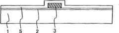
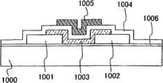
例如,在对比文件1中公开了对于沟道形成区域使用ZnO的半导体器件。参照图7A说明使用ZnO的半导体器件的结构。For example,
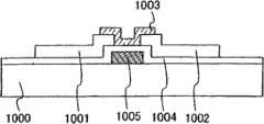
图7A中的半导体器件在诸如玻璃衬底的绝缘衬底1000之上具有源电极1001、漏电极1002、被配置为与源电极1001和漏电极1002接触的ZnO层1003、层叠在ZnO层1003之上的栅绝缘层1004和栅电极1005。The semiconductor device in FIG. 7A has a
对于源电极1001和漏电极1002,使用导电的ZnO。导电的ZnO掺杂有以下的元素中的一种:作为第III族元素的B(硼)、Al(铝)、镓(Ga)、铟(In)或Tl(铊);作为第VII族元素的F(氟)、Cl(氯)、Br(溴)或I(碘);作为第I族元素的锂(Li)、Na(钠)、K(钾)、Rb(铷)或Cs(铯);作为第V族元素的N(氮)、P(磷)、As(砷)、Sb(锑)或Bi(铋)。For the
[参考文件]日本公开专利申请No.2000-150900[Reference Document] Japanese Laid-Open Patent Application No.2000-150900
发明内容Contents of the invention
根据本发明的发明人的试验,揭示了当通过蚀刻形成图7A所示的顶栅半导体器件的源电极1001和漏电极1002时衬底1000在一些情况下被蚀刻。即使在形成通过在衬底1000上使用氧化硅膜或氧氮化硅膜形成的基膜1006的情况下,当基膜被蚀刻时衬底1000的表面也在一些情况下被露出。另外,在图7B所示的底栅半导体器件的情况下,揭示了当通过蚀刻形成源电极1001和漏电极1002时通过使用氧化硅膜或氧氮化硅膜形成的栅绝缘膜1004被蚀刻。According to experiments by the inventors of the present invention, it was revealed that
在顶栅半导体器件的情况下,当玻璃衬底1000或通过使用氧化硅膜或氧氮化硅膜形成的基膜1006被蚀刻时,诸如钠的杂质从衬底1000扩散到半导体膜1003中,使得特性劣化。In the case of a top-gate semiconductor device, when the
在底栅半导体器件(图7B)的情况下,如果当通过蚀刻形成源电极1001和漏电极1002时栅绝缘膜1004被蚀刻,那么特性是不稳定的并且导致故障。In the case of a bottom-gate semiconductor device ( FIG. 7B ), if the
考虑到以上情况,本发明的目的是,提供即使对沟道形成区域使用ZnO半导体膜并且对于源电极和漏电极使用其中添加n型或p型杂质的ZnO膜也不产生缺陷或故障的半导体器件及其制造方法。In view of the above circumstances, an object of the present invention is to provide a semiconductor device in which defects or failures do not occur even if a ZnO semiconductor film is used for a channel formation region and a ZnO film in which an n-type or p-type impurity is added is used for a source electrode and a drain electrode and methods of manufacture thereof.
本发明的半导体器件的一个方面具有:在氧化硅膜或氧氮化硅膜之上的Al膜或Al合金膜和在Al膜或Al合金膜之上的其中添加n型或p型杂质的ZnO膜。本说明书中的“氧化硅膜”、“氧氮化硅膜”、“Al膜”、“Al合金膜”和“ZnO膜”分别意味着包含氧化硅的膜、包含氧氮化硅的膜、包含Al的膜、包含Al合金的膜和包含ZnO的膜。One aspect of the semiconductor device of the present invention has: an Al film or an Al alloy film over a silicon oxide film or a silicon oxynitride film, and ZnO in which n-type or p-type impurities are added over the Al film or Al alloy film membrane. "Silicon oxide film", "silicon oxynitride film", "Al film", "Al alloy film" and "ZnO film" in this specification mean a film containing silicon oxide, a film containing silicon oxynitride, A film containing Al, a film containing an Al alloy, and a film containing ZnO.
本发明的半导体器件的一个方面具有:在栅电极之上的通过使用氧化硅膜或氧氮化硅膜形成的栅绝缘膜、在栅绝缘膜之上的Al膜或Al合金膜、在Al膜或Al合金膜之上的其中添加n型或p型杂质的ZnO膜、以及在其中添加n型或p型杂质的ZnO膜和栅绝缘膜之上的ZnO半导体膜。One aspect of the semiconductor device of the present invention has: a gate insulating film formed by using a silicon oxide film or a silicon oxynitride film over the gate electrode, an Al film or an Al alloy film over the gate insulating film, an Al film or a ZnO film to which n-type or p-type impurities are added over an Al alloy film, and a ZnO film to which n-type or p-type impurities are added and a ZnO semiconductor film over a gate insulating film.
本发明的半导体器件的一个方面具有:在氧化硅膜或氧氮化硅膜之上的Al膜或Al合金膜、在Al膜或Al合金膜之上的其中添加n型或p型杂质的ZnO膜、在氧化硅膜或氧氮化硅膜和其中添加n型或p型杂质的ZnO膜之上的ZnO半导体膜、在ZnO半导体膜之上的栅绝缘膜、和在栅绝缘膜之上的栅电极。One aspect of the semiconductor device of the present invention has: an Al film or an Al alloy film over a silicon oxide film or a silicon oxynitride film, and ZnO in which n-type or p-type impurities are added over the Al film or Al alloy film film, a ZnO semiconductor film over a silicon oxide film or a silicon oxynitride film and a ZnO film to which n-type or p-type impurities are added, a gate insulating film over the ZnO semiconductor film, and a gate insulating film over the gate electrode.
本发明的半导体器件的制造方法的一个方面具有以下步骤:形成氧化硅膜或氧氮化硅膜;在氧化硅膜或氧氮化硅膜之上形成Al膜或Al合金膜;在Al膜或Al合金膜之上形成其中添加n型或p型杂质的ZnO膜,其中,其中添加n型或p型杂质的ZnO膜通过第一蚀刻被蚀刻为具有岛状形状,并且Al膜或Al合金膜通过第二蚀刻被蚀刻为具有岛状形状。One aspect of the manufacturing method of the semiconductor device of the present invention has the following steps: forming a silicon oxide film or a silicon oxynitride film; forming an Al film or an Al alloy film on the silicon oxide film or the silicon oxynitride film; A ZnO film in which n-type or p-type impurities are added is formed over the Al alloy film, wherein the ZnO film in which n-type or p-type impurities are added is etched to have an island-like shape by the first etching, and the Al film or the Al alloy film It is etched to have an island shape by the second etching.
本发明的半导体器件的制造方法的一个方面,其中,在第二蚀刻之后,在其中添加n型或p型杂质的ZnO膜、和氧化硅膜或氧氮化硅膜之上形成ZnO半导体膜。An aspect of the method of manufacturing a semiconductor device of the present invention, wherein, after the second etching, a ZnO semiconductor film is formed over the ZnO film to which n-type or p-type impurities are added, and the silicon oxide film or silicon oxynitride film.
在底栅半导体器件的情况下,在形成栅电极之后,在栅电极之上形成通过使用氧化硅膜或氧氮化硅膜形成的栅绝缘膜。In the case of a bottom-gate semiconductor device, after forming a gate electrode, a gate insulating film formed by using a silicon oxide film or a silicon oxynitride film is formed over the gate electrode.
在顶栅半导体器件的情况下,在形成ZnO半导体膜之后形成栅绝缘膜并且形成栅电极。In the case of a top-gate semiconductor device, a gate insulating film is formed and a gate electrode is formed after the ZnO semiconductor film is formed.
本发明的第一蚀刻可以是湿蚀刻。The first etching of the present invention may be wet etching.
本发明的第一蚀刻可以是使用缓冲的氢氟酸的湿蚀刻。The first etch of the present invention may be a wet etch using buffered hydrofluoric acid.
本发明的第一蚀刻可以是干蚀刻。The first etching of the present invention may be dry etching.
本发明的第一蚀刻可以是使用CH4(甲烷)气体的干蚀刻。The first etching of the present invention may be dry etching using CH4 (methane) gas.
本发明的第二蚀刻可以是湿蚀刻。The second etching of the present invention may be wet etching.
本发明的第二蚀刻可以是使用光刻胶的显影溶液的湿蚀刻。The second etching of the present invention may be wet etching using a developing solution of a photoresist.
本发明的第二蚀刻可以是使用有机碱溶液的湿蚀刻。The second etching of the present invention may be wet etching using an organic alkali solution.
本发明的第二蚀刻可以是使用TMAH(四甲基氢氧化铵)的湿蚀刻。The second etching of the present invention may be wet etching using TMAH (tetramethylammonium hydroxide).
本发明的半导体器件的一个方面具有:栅电极、在栅电极之上的栅绝缘膜、在栅绝缘膜之上的包含金属材料的第一膜、在第一膜之上的包含透明半导体材料和n型或p型杂质的第二膜、以及在第二膜和栅绝缘膜之上的包含透明半导体材料的第三膜。One aspect of the semiconductor device of the present invention has: a gate electrode, a gate insulating film over the gate electrode, a first film containing a metal material over the gate insulating film, a transparent semiconductor material over the first film, and A second film of n-type or p-type impurities, and a third film containing a transparent semiconductor material over the second film and the gate insulating film.
本发明的半导体器件的一个方面具有:在衬底之上的绝缘膜、在绝缘膜之上的包含金属材料的第一膜、在金属膜之上的包含透明半导体材料和n型或p型杂质的第二膜、在绝缘膜和第二膜之上的包含透明半导体材料的第三膜、在第三膜之上的栅绝缘膜、和在栅绝缘膜之上的栅电极。One aspect of the semiconductor device of the present invention has: an insulating film over a substrate, a first film containing a metal material over the insulating film, a first film containing a transparent semiconductor material and an n-type or p-type impurity over the metal film a second film, a third film containing a transparent semiconductor material over the insulating film and the second film, a gate insulating film over the third film, and a gate electrode over the gate insulating film.
本发明的半导体器件的制造方法的一个方面具有以下步骤:在衬底之上形成绝缘膜;在绝缘膜之上形成包含金属材料的第一膜;在第一膜之上形成包含透明半导体材料和n型或p型杂质的第二膜;蚀刻第二膜;和蚀刻第一膜。One aspect of the method of manufacturing a semiconductor device of the present invention has the steps of: forming an insulating film over a substrate; forming a first film containing a metal material over the insulating film; forming a film containing a transparent semiconductor material and the second film of n-type or p-type impurities; etching the second film; and etching the first film.
本发明的半导体器件的制造方法的一个方面具有以下步骤:在衬底之上形成栅电极;在栅电极之上形成栅绝缘膜;在栅绝缘膜之上形成包含金属材料的第一膜;在第二膜之上形成包含透明半导体材料和n型或p型杂质的第二膜;蚀刻第二膜;和蚀刻第一膜。One aspect of the method of manufacturing a semiconductor device of the present invention has the steps of: forming a gate electrode over a substrate; forming a gate insulating film over the gate electrode; forming a first film containing a metal material over the gate insulating film; forming a second film containing a transparent semiconductor material and n-type or p-type impurities over the second film; etching the second film; and etching the first film.
在顶栅半导体器件中,通过使用玻璃衬底、氧化硅膜或氧氮化硅膜形成的基膜不被蚀刻,并且诸如钠的杂质不从衬底扩散到半导体膜中,使得其特性不劣化。In a top-gate semiconductor device, a base film formed by using a glass substrate, a silicon oxide film, or a silicon oxynitride film is not etched, and impurities such as sodium do not diffuse from the substrate into the semiconductor film, so that its characteristics are not deteriorated .
在底栅半导体器件中,栅绝缘膜不被蚀刻并且其特性不会变得不稳定。In a bottom-gate semiconductor device, the gate insulating film is not etched and its characteristics do not become unstable.
由于对于源电极和漏电极的一部分使用Al,因此可以获得低电阻的引线。Since Al is used for a part of the source electrode and the drain electrode, a low-resistance lead can be obtained.
附图说明Description of drawings
在附图中,In the attached picture,
图1A和图1B表示本发明的半导体器件;Figure 1A and Figure 1B represent the semiconductor device of the present invention;
图2A~2D表示本发明的半导体器件的制造步骤;2A~2D represent the manufacturing steps of the semiconductor device of the present invention;
图3A~3D表示本发明的半导体器件的制造步骤;3A~3D represent the manufacturing steps of the semiconductor device of the present invention;
图4A和图4B表示本发明的半导体器件的制造步骤;4A and 4B represent the manufacturing steps of the semiconductor device of the present invention;
图5A~5D表示本发明的半导体器件的制造步骤;5A-5D represent the manufacturing steps of the semiconductor device of the present invention;
图6A~6C表示本发明的半导体器件的制造步骤;6A~6C represent the manufacturing steps of the semiconductor device of the present invention;
图7A和图7B表示常规的例子;7A and 7B represent conventional examples;
图8A和图8B表示液晶显示器的制造步骤;8A and 8B represent the manufacturing steps of the liquid crystal display;
图9A和图9B表示液晶显示器的制造步骤;9A and 9B represent the manufacturing steps of the liquid crystal display;
图10A和图10B表示发光器件的制造步骤;10A and 10B represent the manufacturing steps of the light emitting device;
图11A和图11B表示发光器件的制造步骤;11A and 11B represent the manufacturing steps of the light emitting device;
图12A~12F分别表示发光器件的等效电路。12A to 12F each show an equivalent circuit of a light emitting device.
图13表示发光器件的等效电路。Fig. 13 shows an equivalent circuit of a light emitting device.
图14A表示像素部分的顶部前视图,图14B表示发光器件的等效电路;FIG. 14A shows a top front view of a pixel portion, and FIG. 14B shows an equivalent circuit of a light emitting device;
图15A~15E分别表示应用本发明的电子装置的例子;15A to 15E respectively represent an example of an electronic device applying the present invention;
图16表示应用本发明的电子装置的例子。FIG. 16 shows an example of an electronic device to which the present invention is applied.
以下参照附图说明本发明的实施例。注意,本发明不限于以下的说明,并且本领域技术人员很容易理解可以在不背离本发明的目的和范围的条件下以各种方式修改这里公开的实施例和细节。因此,本发明不应被解释为限于以下给出的实施例的说明。Embodiments of the present invention will be described below with reference to the drawings. Note that the present invention is not limited to the following description, and it is easily understood by those skilled in the art that the embodiments and details disclosed herein can be modified in various ways without departing from the purpose and scope of the present invention. Therefore, the present invention should not be construed as being limited to the description of the Examples given below.
具体实施方式Detailed ways
[实施例1][Example 1]
这里说明底栅半导体器件。A bottom-gate semiconductor device is explained here.
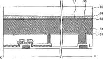
图1A是示出本发明的实施例的一个例子的截面图。在图1A中,附图标记1表示衬底,3表示栅电极,5表示栅绝缘膜、10表示源电极,10a表示第一导电膜,10b表示第二导电膜,11表示漏电极,11a表示第一导电膜,11b表示第二导电膜,13表示半导体膜。可以在半导体膜13之上形成用于钝化或平坦化的绝缘膜。FIG. 1A is a cross-sectional view showing an example of an embodiment of the present invention. In FIG. 1A,
在衬底1之上形成栅电极3,在栅电极3之上形成栅绝缘膜5,并且在栅绝缘膜5之上形成源电极10和漏电极11。源电极10由具有第一导电膜10a与第二导电膜10b的叠层膜形成,并且漏电极11由具有第一导电膜11a与第二导电膜11b的叠层膜形成。可以在第一导电膜10a和第二导电膜10b之间或者在第一导电膜11a和第二导电膜11b之间形成第三导电膜。源电极10和漏电极11可分别形成为通过栅绝缘膜5与栅电极3部分重叠。在源电极10之上形成半导体膜13并且在栅绝缘膜5之上形成漏电极11。
这里说明各结构。Each structure will be described here.
(1)衬底(1) Substrate
对于形成衬底,可以使用通过使用玻璃衬底形成的衬底、诸如氧化铝的绝缘材料和可以在后续步骤中抵抗处理温度的塑料衬底等。在对于衬底1使用塑料衬底的情况下,可以使用PC(聚碳酸酯)、PES(聚醚砜)、PET(聚对苯二甲酸乙二酯)或PEN(聚萘二甲酸乙二酯)等。在塑料衬底的情况下,可以在表面的上方设置无机层或有机层作为的气体阻挡层。在在塑料衬底的制造过程中在衬底上产生由灰尘等形成的突出物的情况下,可以在用CMP等抛光衬底以使其表面平坦化之后使用该衬底。可以在衬底1之上形成用于防止杂质等从衬底侧扩散的诸如氧化硅(SiOx)、氮化硅(SiNx)、氧氮化硅(SiOxNy)(x>y)和氮氧化硅(SiNxOy)(x>y)的绝缘膜。For forming the substrate, a substrate formed by using a glass substrate, an insulating material such as alumina, a plastic substrate that can withstand a processing temperature in a subsequent step, and the like can be used. In the case of using a plastic substrate for the
(2)栅电极(2) Gate electrode
可以通过使用Al(铝)膜、W(钨)膜、Mo(钼)膜、Ta(钽)膜、Cu(铜)膜、Ti(钛)膜或包含这些元素作为主要成分的合金材料(例如,Al合金膜、MoW(钼钨)合金膜)等形成栅电极。可以使用以掺杂有诸如P(磷)的杂质元素的多晶硅膜为代表的半导体膜。栅电极3可以是单层或其中层叠两层或更多层的叠层膜。By using an Al (aluminum) film, a W (tungsten) film, a Mo (molybdenum) film, a Ta (tantalum) film, a Cu (copper) film, a Ti (titanium) film, or an alloy material containing these elements as a main component (e.g. , Al alloy film, MoW (molybdenum-tungsten) alloy film) etc. form the gate electrode. A semiconductor film typified by a polysilicon film doped with an impurity element such as P (phosphorus) can be used. The
(3)栅绝缘膜(3) Gate insulating film
可以通过使用例如氧化硅膜和氧氮化硅膜的包含硅作为主要成分的绝缘膜形成栅绝缘膜5。另外,它可以是单层或叠层膜。
(4)源电极和漏电极(4) Source and drain electrodes
源电极10由第一导电膜10a与第二导电膜10b的叠层膜形成,并且漏电极11由第一导电膜11a与第二导电膜11b的叠层膜形成。The
作为第一导电膜,可以使用Al膜、诸如AlNi(铝镍)膜和AlNd(钕铝)膜的Al合金膜。作为第二导电膜,可以使用其中添加B(硼)、Al(铝)、Ga(镓)、P(磷)或As(砷)的p型或n型杂质的ZnO(氧化锌)。可以在第一导电膜和第二导电膜之间设置诸如Ti膜的金属膜作为第三导电膜。As the first conductive film, an Al film, an Al alloy film such as an AlNi (aluminum nickel) film and an AlNd (neodymium aluminum) film can be used. As the second conductive film, ZnO (zinc oxide) to which a p-type or n-type impurity of B (boron), Al (aluminum), Ga (gallium), P (phosphorus), or As (arsenic) is added can be used. A metal film such as a Ti film may be provided as the third conductive film between the first conductive film and the second conductive film.
(5)半导体膜(5) Semiconductor film
使用ZnO膜作为半导体膜。由于与半导体膜接触的源电极和漏电极具有其中添加p型或n型杂质的ZnO膜,因此它们可以很容易地与半导体膜连接。A ZnO film is used as the semiconductor film. Since the source and drain electrodes in contact with the semiconductor film have a ZnO film in which p-type or n-type impurities are added, they can be easily connected to the semiconductor film.
(6)绝缘膜(6) Insulating film
虽然没有示出,但可以在半导体膜13之上形成诸如钝化膜和平坦化膜的绝缘膜。可以使用氧化硅(SiOx)、氮化硅(SiNx)、氧氮化硅(SiOxNy)(x>y)和氮氧化硅(SiNxOy)(x>y)、SOG(旋涂玻璃)膜或丙烯的有机树脂膜或它们的叠层膜。Although not shown, an insulating film such as a passivation film and a planarization film may be formed over the
在底栅半导体器件中,栅绝缘膜在制造过程中不被蚀刻,并且特性不会变得不稳定。对于源电极和漏电极的一部分使用Al,由此实现低电阻的引线。In a bottom-gate semiconductor device, the gate insulating film is not etched during the manufacturing process, and characteristics do not become unstable. Al is used for a part of the source electrode and the drain electrode, thereby realizing a low-resistance lead.
[实施例2][Example 2]
这里说明顶栅半导体器件。Here, a top-gate semiconductor device is explained.
图1B是示出本发明的实施例的一个例子的截面图。在图1B中,附图标记1表示衬底,20表示绝缘膜、25表示源电极,25a表示第一导电膜,25b表示第二导电膜,26表示漏电极,26a表示第一导电膜,26b表示第二导电膜,27表示半导体膜,28表示栅绝缘膜,29表示栅电极。可以在栅电极之上形成用于钝化或平坦化的绝缘膜。FIG. 1B is a cross-sectional view showing an example of an embodiment of the present invention. In FIG. 1B,
在衬底1上形成绝缘膜20,并且在绝缘膜20之上形成源电极25和漏电极26。源电极25由第一导电膜25a与第二导电膜25b的叠层膜形成,并且漏电极26由第一导电膜26a与第二导电膜26b的叠层膜形成。可以在第一导电膜25a和第二导电膜25b之间或者在第一导电膜26a和第二导电膜26b之间形成第三导电膜。在源电极25之上形成半导体膜27并且在绝缘膜20之上形成漏电极26,在半导体膜27之上形成栅绝缘膜28,并且在栅绝缘膜28之上形成栅电极29。栅电极29可形成为与源电极和漏电极部分重叠,使得栅绝缘膜28和半导体膜27被插入它们之间。An insulating
这里说明各结构。Each structure will be described here.
对于衬底,可以使用与在实施例1中说明的那些相同的源电极、漏电极、半导体膜和栅电极。For the substrate, the same source electrode, drain electrode, semiconductor film, and gate electrode as those explained in
(1)在衬底之上的绝缘膜(1) Insulating film over substrate
在衬底1之上形成氧化硅膜和氧氮化硅膜作为用于防止杂质等从衬底侧扩散的绝缘膜20。另外,它可以是单层或叠层膜。A silicon oxide film and a silicon oxynitride film are formed over the
(2)栅绝缘膜(2) Gate insulating film
可以通过使用例如氧化硅膜、氧氮化硅膜、氮氧化硅膜和氮化硅膜的包含硅作为主要成分的绝缘膜形成栅绝缘膜28。另外,它可以是单层或叠层膜。The
(3)在栅电极之上的绝缘膜(3) Insulating film over the gate electrode
虽然没有示出,但在栅电极29之上形成诸如钝化膜和平坦化膜的层间绝缘膜。可以使用SiOx膜、SiNx膜、SiON膜、SiNO膜、SOG(旋涂玻璃)膜和丙烯的有机树脂膜或它们的叠层膜。Although not shown, an interlayer insulating film such as a passivation film and a planarization film is formed over the
在顶栅半导体器件中,衬底或通过使用氧化硅膜或氧氮化硅膜形成的基膜不被蚀刻,使得诸如钠的杂质不从衬底扩散到半导体膜中,并且特性不劣化。对于源电极和漏电极的一部分使用Al,由此实现低电阻的引线。In a top-gate semiconductor device, a substrate or a base film formed by using a silicon oxide film or a silicon oxynitride film is not etched, so that impurities such as sodium do not diffuse from the substrate into the semiconductor film, and characteristics do not deteriorate. Al is used for a part of the source electrode and the drain electrode, thereby realizing a low-resistance lead.
[实施例3][Example 3]
说明底栅半导体器件的制造方法,其中,在栅电极之上形成氧化硅膜或氧氮化硅膜作为栅绝缘膜,形成Al膜或Al合金膜作为第一导电膜,形成其中添加n型或p型杂质的ZnO膜作为第二导电膜,然后,第二导电膜通过第一蚀刻被蚀刻为具有岛状形状并且第一导电膜通过第二蚀刻被蚀刻为具有岛状形状以形成源电极和漏电极,并且,形成ZnO半导体膜。A method for manufacturing a bottom-gate semiconductor device is described, wherein a silicon oxide film or a silicon oxynitride film is formed as a gate insulating film over a gate electrode, an Al film or an Al alloy film is formed as a first conductive film, and an n-type or A ZnO film of p-type impurity is used as the second conductive film, and then, the second conductive film is etched to have an island-like shape by first etching and the first conductive film is etched to have an island-like shape by second etching to form the source electrode and A drain electrode, and a ZnO semiconductor film is formed.
如图2A所示,形成栅电极3。在衬底1之上的栅电极的厚度可以为10~200nm。可以通过使用实施例1所示的材料形成衬底1。这里,使用玻璃衬底。As shown in FIG. 2A,
可以通过CVD或溅射形成厚度为10~200nm的包含氧化硅(SiOx)、氮化硅(SiNx)、氧氮化硅(SiOxNy)(x>y)和氮氧化硅(SiNxOy)(x>y)的绝缘膜2,以防止杂质等从衬底侧扩散(图2B)。Silicon oxide (SiOx), silicon nitride (SiNx), silicon oxynitride (SiOxNy) (x>y) and silicon oxynitride (SiNxOy) (x>y) can be formed by CVD or sputtering with a thickness of 10-200nm. ) to prevent the diffusion of impurities and the like from the substrate side (FIG. 2B).
可以通过用高密度等离子处理衬底1的表面形成绝缘膜2。例如,可以通过使用2.45GHz的微波产生高密度等离子,并且仅要求电子密度为1×10¹¹~1×10¹³/cm3并且电子温度为2eV或更低。这种高密度等离子具有较低的动能的活性物质,并且,与常规的等离子处理相比,可以形成由等离子造成的损伤更少的具有更少的缺陷的膜。Insulating
可以在诸如包含氮气和惰性气体的气氛,包含氮气、氢气和惰性气体的气氛,以及包含氨气和惰性气体的气氛的氮化气氛下通过高密度等离子处理氮化衬底1的表面。在使用玻璃衬底作为经受高密度等离子氮化处理的衬底1的情况下,作为在衬底1的表面之上形成的氮化物膜,可以形成包含氮化硅作为主要成分的绝缘膜2。可以通过使用通过等离子CVD在氮化物膜的上方形成氧化硅膜或氧氮化硅膜的多个层来形成绝缘膜2。The surface of
另外,可以类似地通过用高密度等离子在绝缘膜2的表面之上进行氮化形成氮化物膜。In addition, a nitride film can be similarly formed by nitriding over the surface of the insulating
通过用高密度等离子氮化形成的氮化物膜可抑制杂质从衬底1的扩散。Diffusion of impurities from
可以通过使用实施例1所示的材料形成栅电极3。这里,通过使用AlNd(铝钕)靶材的溅射形成AlNd膜并将其处理成岛状形状。对于将膜处理成岛状形状,使用光刻方法,并且使用干蚀刻或湿蚀刻。
在清洗栅电极3的表面和衬底1或绝缘膜2的表面之后,在栅电极3之上通过使用已知的CVD或溅射形成厚度为10~200nm的栅绝缘膜5(图2A和图2B)。可以在不暴露于空气的情况下连续实施表面清洗步骤和栅绝缘膜5的形成步骤。在对于栅电极3使用Al膜的情况下,当在高温下形成栅绝缘膜5时,在一些情况下产生隆起(hillock)。因此,优选地,在500℃或更低、优选350℃或更低的低温下形成膜。After cleaning the surface of the
可以通过使用实施例1所示的材料形成栅绝缘膜5。这里,形成氧化硅膜。注意,在以下的附图中省略绝缘膜2。
在栅绝缘膜5上形成厚度为10~200nm的用于源电极和漏电极的第一导电膜6。可以通过使用实施例1所示的材料形成第一导电膜6。这里,使用AlNi(铝镍)膜或AlNd膜。可以通过使用AlNi靶材或AlNd靶材的溅射形成第一导电膜6。在形成栅绝缘膜5之后,可以在不暴露于空气的情况下连续形成第一导电膜6。A first conductive film 6 for source and drain electrodes is formed on the
在第一导电膜6上形成厚度为10~200nm的第二导电膜7(图2C)。可以通过使用实施例1所示的材料形成7。这里,使用其中添加诸如Al或Ga的杂质的ZnO(氧化锌)。因此,可以很容易地在第二导电膜7和后面形成为半导体层的ZnO膜之间产生欧姆接触。可以通过使用溅射形成第二导电膜7。例如,对于添加Al或Ga可以使用以下的方法:使用其中添加1~10重量%的Al或Ga的ZnO靶材的溅射;或在200~300℃下在ZnO靶材上安装Al或Ga芯片的溅射。A second conductive film 7 is formed on the first conductive film 6 with a thickness of 10 to 200 nm (FIG. 2C). 7 can be formed by using the materials shown in Example 1. Here, ZnO (zinc oxide) to which impurities such as Al or Ga are added is used. Therefore, ohmic contact can be easily produced between the second conductive film 7 and the ZnO film formed later as a semiconductor layer. The second conductive film 7 can be formed by using sputtering. For example, the following methods can be used for adding Al or Ga: sputtering using a ZnO target in which 1 to 10% by weight of Al or Ga is added; or mounting an Al or Ga chip on a ZnO target at 200 to 300°C of sputtering.
在形成第一导电膜6之后,可以在不暴露于空气的情况下连续形成第二导电膜7。因此,可以在不暴露于空气的情况下连续实施从栅绝缘膜5到第二导电膜7的形成。After the first conductive film 6 is formed, the second conductive film 7 can be continuously formed without exposure to air. Therefore, the formation from the
在第一导电膜6和第二导电膜7之间形成厚度为10~200nm的第三导电膜8(图2D)。接触电阻根据制造过程中的热处理温度在第一导电膜6和第二导电膜7之间偶尔增加。但是,通过形成第三导电膜8,可减小第一导电膜6与第二导电膜7之间的接触电阻。可以通过使用诸如通过溅射等形成的Ti膜的金属膜形成第三导电膜8。A third conductive film 8 having a thickness of 10 to 200 nm is formed between the first conductive film 6 and the second conductive film 7 (FIG. 2D). The contact resistance occasionally increases between the first conductive film 6 and the second conductive film 7 according to the heat treatment temperature in the manufacturing process. However, by forming the third conductive film 8, the contact resistance between the first conductive film 6 and the second conductive film 7 can be reduced. Third conductive film 8 can be formed by using a metal film such as a Ti film formed by sputtering or the like.
在第二导电膜7之上形成光刻胶掩模9,并且第二导电膜7被蚀刻(图3A和图3B)。在使用湿蚀刻的情况下,使用例如HF∶NH4F(重量比)=1∶100~1∶10的溶液的缓冲的氢氟酸(其中混合了HF(氢氟酸)和NH4F(氟化氨))。A photoresist mask 9 is formed over the second conductive film 7, and the second conductive film 7 is etched (FIGS. 3A and 3B). In the case of using wet etching, buffered hydrofluoric acid (in which HF (hydrofluoric acid) andNH 4F ( ammonium fluoride)).
在使用干蚀刻的情况下,可以采用使用CH4气体的各向异性等离子蚀刻。In the case of using dry etching, anisotropic plasma etching using CH4 gas can be employed.
在第二导电膜7之下形成第一导电膜6。因此,当第二导电膜7被蚀刻时,第一导电膜6用作蚀刻阻止层。因此,在蚀刻中可以在不损伤栅绝缘膜5的情况下形成源电极和漏电极。The first conductive film 6 is formed under the second conductive film 7 . Therefore, when the second conductive film 7 is etched, the first conductive film 6 functions as an etching stopper. Therefore, the source electrode and the drain electrode can be formed without damaging the
当第二导电膜7被蚀刻时,第一导电膜6的一部分会被蚀刻。但是,由于如果第一导电膜6被完全蚀刻,则栅绝缘膜受损,因此需要注意不要完全蚀刻第一导电膜6。When the second conductive film 7 is etched, a part of the first conductive film 6 is etched. However, since the gate insulating film is damaged if the first conductive film 6 is completely etched, care needs to be taken not to completely etch the first conductive film 6 .
然后,通过使用光刻胶掩模9蚀刻第一导电膜6形成源电极10和漏电极11(图3C)。在本发明中,通过使用以作为光刻胶的显影剂的TMAH(四甲基氢氧化铵)为代表的有机碱溶液蚀刻第一导电膜6。Then,
在对于第一导电膜6使用AlNi膜并且对于蚀刻溶液使用TMAH的情况下,在30℃下蚀刻速率为约300nm/min。另一方面,使用上述材料的第二导电膜7或栅绝缘膜5不被TMAH蚀刻。因此,可以在不损伤栅绝缘膜5的情况下形成源电极10和漏电极11。并且,岛状形状的第二导电膜10b和11b的尺寸不会减小。在本发明中,可以通过使用当在不使用特定的蚀刻溶液的情况下形成光刻胶掩模时使用的显影剂蚀刻第一导电膜6。因此,成本降低并且效率增加。In the case of using the AlNi film for the first conductive film 6 and using TMAH for the etching solution, the etching rate was about 300 nm/min at 30°C. On the other hand, the second conductive film 7 or the
在形成源电极10和漏电极11之后,光刻胶掩模9被去除。After the
在源电极10、漏电极11和栅绝缘膜5之上通过溅射形成厚度为20~200nm的ZnO膜作为半导体膜12(图3D)。例如,可以在200~300℃下通过使用ZnO靶材、氧气/氩气的流量比为30~20的溅射形成膜。A ZnO film having a thickness of 20 to 200 nm is formed as a
通过光刻方法蚀刻半导体膜12以形成岛状形状的半导体膜13(图4A)。可以采用使用缓冲的氢氟酸的湿蚀刻方法或使用CH4气体的各向异性干蚀刻方法。The
在半导体膜12和第二导电膜10b和11b中通常使用ZnO,并且,难以获得足够的蚀刻选择性。但是,由于要求在与半导体膜12接触的一部分中形成第二导电膜7,因此可以在例如引线部分的不与半导体膜12接触的一部分中蚀刻第二导电膜7。在上述的蚀刻方法中,第二导电膜10b和11b可被蚀刻,但第一导电膜10a和11a不被蚀刻。因此,第一导电膜10a和11a用作引线,并且与半导体器件的电连接得到保证。ZnO is generally used in the
通过CVD或溅射在半导体膜13之上形成厚度为50nm~1μm的绝缘膜14(图4B)。可以形成包含硅作为主要成分的绝缘膜作为绝缘膜14。可以在包含硅的绝缘膜之上层叠有机树脂膜等。绝缘膜14用作平坦化膜或钝化膜。由于在源电极10和漏电极11内包含Al,因此当在高温下形成绝缘膜14时偶尔产生隆起。因此,优选地,在500℃或更低、优选350℃或更低的低温下形成。An insulating
在绝缘膜14中形成接触孔,并且,如有必要设置与栅电极3、源电极10和漏电极11接触的导电膜。A contact hole is formed in the insulating
根据本发明,在不损伤栅绝缘膜的情况下形成半导体器件。使用诸如AlNi膜的Al合金膜作为第一导电膜,由此实现低电阻的引线。According to the present invention, a semiconductor device is formed without damaging the gate insulating film. An Al alloy film such as an AlNi film is used as the first conductive film, thereby realizing a low-resistance lead.
[实施例4][Example 4]
这里,说明顶栅半导体器件的制造方法,其中,在氧化硅膜或氧氮化硅膜上形成Al膜或Al合金膜作为第一导电膜,并且形成其中添加n型或p型杂质的ZnO膜作为第二导电膜,然后,第二导电膜通过第一蚀刻形成为具有岛状形状,第一导电膜通过第二蚀刻形成为具有岛状形状以形成源电极和漏电极,形成ZnO半导体膜,形成栅绝缘膜,并且形成栅电极。注意,不用说,在实施例1~3中说明的材料和制造方法可被应用于本实施例。Here, a method of manufacturing a top-gate semiconductor device is described in which an Al film or an Al alloy film is formed as a first conductive film on a silicon oxide film or a silicon oxynitride film, and a ZnO film to which n-type or p-type impurities are added is formed. As the second conductive film, then, the second conductive film is formed to have an island-like shape by first etching, the first conductive film is formed to have an island-like shape by second etching to form a source electrode and a drain electrode, a ZnO semiconductor film is formed, A gate insulating film is formed, and a gate electrode is formed. Note that it goes without saying that the materials and manufacturing methods described in
如图5A所示,通过CVD或溅射以10~200nm的厚度在衬底1之上形成氧化硅(SiOx)膜作为绝缘膜20。绝缘膜20防止杂质等从衬底1侧扩散。As shown in FIG. 5A, a silicon oxide (SiOx) film is formed as an insulating
在绝缘膜20之上通过溅射或蒸镀形成厚度为10~200nm的用于源电极和漏电极的第一导电膜21。可以使用诸如在实施例1中示出的AlNi(铝镍)膜的Al合金膜作为第一导电膜21。在形成绝缘膜20之后,可以在不暴露于空气的情况下连续形成第一导电膜21。A first
在第一导电膜21上通过溅射形成厚度为10~200nm的第二导电膜22(图5A)。作为第二导电膜22,可以使用其中添加B(硼)、Al(铝)、Ga(镓)、P(磷)或As(砷)等的p型或n型杂质的ZnO(氧化锌)。在形成第一导电膜21之后,可在不暴露于空气的情况下连续形成第二导电膜22。因此,可以在不暴露于空气的情况下连续实施形成绝缘膜20到第二导电膜22的步骤。A second
为了减小第一导电膜21与第二导电膜22之间的接触电阻,可以在第一导电膜21和第二导电膜22之间通过溅射形成厚度为10~200nm的诸如Ti膜的金属膜作为第三导电膜23(图5B)。In order to reduce the contact resistance between the first
在第二导电膜22之上形成光刻胶掩模24,并且蚀刻第二导电膜22(图5C)。作为蚀刻方法,可以采用使用缓冲的氢氟酸的湿蚀刻或使用CH4气体的干蚀刻方法。A
在第二导电膜22之下形成第一导电膜21。因此,当第二导电膜22被蚀刻时,第一导电膜21用作蚀刻阻止层。因此,可以在不通过蚀刻绝缘膜20露出衬底1的情况下形成源电极和漏电极。The first
当第二导电膜22被蚀刻时,第一导电膜21的一部分可被蚀刻。注意,如果所有的第一导电膜21被蚀刻,那么绝缘膜20被蚀刻并且衬底1被露出,这会导致在衬底1中包含的杂质的扩散。When the second
第一导电膜21被蚀刻以形成源电极25和漏电极26(图5D)。作为蚀刻方法,采用使用光刻胶的显影剂TMAH的湿蚀刻。因此,可以在不蚀刻绝缘膜20的情况下形成源电极25和漏电极26。并且,由于ZnO膜不会被TMAH蚀刻,所以岛状形状的第二导电膜25b和26b的尺寸不会减小。可以在不对第一导电膜21使用特殊的蚀刻溶液的情况下用在光刻胶掩模的形成中使用的显影剂进行蚀刻,这导致成本降低和效率提高。The first
在形成源电极25和漏电极26之后,去除光刻胶掩模24。After the
在源电极25、漏电极26和绝缘膜20之上通过溅射形成厚度为20~200nm的ZnO膜作为半导体膜27(图6A)。A ZnO film having a thickness of 20 to 200 nm is formed as a
通过光刻方法蚀刻半导体膜27以制成岛状形状半导体膜27。作为蚀刻方法,可以采用使用缓冲的氢氟酸的湿蚀刻或使用CH4气体的干蚀刻方法。The
对于半导体膜27和第二导电膜25b和26b通常使用ZnO,并且,难以获得较高的蚀刻选择性。但是,由于可与实施例3相同地在源电极和漏电极中形成第二导电膜22,因此可以在不与半导体膜27接触的部分特别是在引线部分中蚀刻第二导电膜。ZnO is generally used for the
在半导体膜27之上通过CVD或溅射形成厚度为10~200nm的栅绝缘膜28(图6B)。半导体膜27可经受在上述的实施例中示出的高密度等离子处理以形成栅绝缘膜。可以在诸如包含氮气和惰性气体的气氛,包含氮气、氢气和惰性气体的气氛和包含氨气和惰性气体的气氛的氮化气氛下通过高密度等离子处理氮化半导体膜27的表面。A
可以通过使用例如氧化硅膜、氧氮化硅膜、氮化硅膜和氮氧化硅膜的包含硅作为主要成分的绝缘膜形成栅绝缘膜28。另外,它可以是单层或叠层膜。The
在栅绝缘膜28之上形成栅电极29(图6B)。可以通过使用上述的实施例所示的材料形成栅电极29,并且它可以是单层或包含两个或更多层的叠层膜。作为用于成膜的方法,可以使用已知的CVD溅射或蒸镀等。对于用光刻方法将栅电极29处理成岛状形状,可以使用干蚀刻或湿蚀刻方法。A
在栅电极29和栅绝缘膜28之上通过CVD或溅射形成厚度为50nm~1μm的绝缘膜30(图6C)。可以通过使用包含硅的绝缘膜形成绝缘膜30。可以在包含硅的绝缘膜之上层叠有机树脂膜等。绝缘膜30用作平坦化膜或钝化膜。由于在源电极25和漏电极26中包含Al,因此,当在高温下形成栅绝缘膜28、栅电极29和绝缘膜30时,偶尔产生隆起(hillock)。因此,优选地,在500℃或更低、优选350℃或更低的低温下形成它们。An insulating film 30 having a thickness of 50 nm to 1 μm is formed by CVD or sputtering over the
如上所述,本发明可防止杂质由于衬底1的露出而扩散。诸如AlNi膜的Al合金膜被用作第一导电膜,由此实现引线的低电阻。As described above, the present invention prevents the diffusion of impurities due to the exposure of the
[实施例5][Example 5]
这里参照图8A和图8B以及图9A和图9B说明通过使用实施例1~3所示的底栅半导体器件制造液晶显示器的方法。注意,不用说,可以应用在实施例2和4中示出的顶栅半导体器件。图8A和图9A表示沿图8B中的线X-Y切取的截面图。Here, a method of manufacturing a liquid crystal display by using the bottom gate semiconductor device shown in
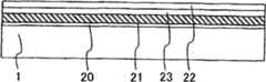
在玻璃衬底或塑料衬底1之上形成栅极引线40和辅助电容器引线41。通过溅射然后通过已知的光刻方法和蚀刻形成AlNd膜。A
通过使用通过CVD或溅射形成的氧化硅膜或氧氮化硅膜形成栅绝缘膜42。The
在栅绝缘膜42之上通过溅射形成AlNi膜作为第一导电膜。第一导电膜在后面形成源电极45a、漏电极46a和源极引线47。An AlNi film is formed as a first conductive film by sputtering over the
在第一导电膜之上通过溅射形成其中添加Al的ZnO(氧化锌)膜作为第二导电膜。第二导电膜在后面形成源电极45b、漏电极46b和源极引线47。A ZnO (zinc oxide) film in which Al was added was formed as a second conductive film by sputtering over the first conductive film. The second conductive film forms the
在第二导电膜(图中未示出)之上,在要成为源电极部分、漏电极部分和源极引线部分的区域中形成光刻胶掩模。然后,蚀刻第二导电膜。这里,通过使用缓冲的氢氟酸即HF∶NH4F=1∶100(重量比)的溶液进行蚀刻。Over the second conductive film (not shown in the figure), a photoresist mask is formed in regions to be the source electrode portion, the drain electrode portion, and the source lead portion. Then, the second conductive film is etched. Here, etching is performed by using buffered hydrofluoric acid, that is, a solution of HF:NH4 F = 1:100 (weight ratio).
然后,通过使用TMAH溶液蚀刻第一导电膜以形成源电极45a、漏电极46a和源极引线47。此后,光刻胶掩模被去除。然后,可以在不损伤栅绝缘膜42的情况下形成源电极45、漏电极46和源极引线47。另外,由于ZnO膜不被TMAH蚀刻,因此岛状形状的第二导电膜的尺寸不会减小。并且,由于AlNi膜被用于第一导电膜,因此源极引线的电阻可减小。Then, the first conductive film was etched by using a TMAH solution to form
然后,形成半导体膜48。通过溅射形成ZnO膜,然后,通过光刻方法和蚀刻从ZnO膜形成半导体膜48。作为蚀刻,采用使用缓冲的氢氟酸的湿蚀刻。这里,由于在要成为引线的部分中形成第一导电膜,因此第二导电膜中的不与半导体膜48接触的部分可被部分去除。Then, a
在半导体膜48之上通过CVD、溅射或涂敷等形成绝缘膜49。可以通过使用具有包含硅的绝缘膜或有机树脂膜等的叠层膜形成绝缘膜49。绝缘膜49可以是使得表面的不均匀性平坦化的膜。An insulating
通过使用光刻方法和蚀刻方法在绝缘膜49中形成通向漏电极46的接触孔和用于辅助电容器的接触孔。A contact hole leading to the
通过溅射形成透明导电膜,然后,通过使用光刻方法和蚀刻形成像素电极50。例如,可以使用ITO(氧化铟锡)、ITSO(包含氧化硅的氧化铟锡)或IZO(氧化铟锌)。A transparent conductive film is formed by sputtering, and then, the
在反射型液晶显示器的情况下,作为透明电极的替代,形成诸如Ag(银)、Au(金)、Cu(铜)、W(钨)或Al(铝)的反光金属材料。In the case of a reflective liquid crystal display, instead of a transparent electrode, a reflective metal material such as Ag (silver), Au (gold), Cu (copper), W (tungsten), or Al (aluminum) is formed.
像素电极50与辅助电容器引线41重叠的部分形成由像素电极50、栅绝缘膜42和辅助电容器引线41形成的辅助电容器100(图8A和图8B)。A portion where the
在引线和电极中,弯曲部分或宽度改变的部分的角可被平滑化和修圆。可以通过使用采用光掩模的图案制造的光掩模图案实现斜切的角的形状。这将具有下述的优点。当进行使用等离子的干蚀刻时,可以通过斜切突出部分来抑制由于异常放电(discharge)导致的细粒子的产生。即使产生细粒子,也可在清洗时防止细粒子在角上蓄积,并且可通过斜切凹进的部分将细粒子洗去。因此,可以解决制造过程中的细粒子或灰尘的问题,并且可提高产量。In lead wires and electrodes, the corners of bent portions or portions where the width changes can be smoothed and rounded. The shape of the chamfered corner can be realized by using a photomask pattern fabricated using the pattern of the photomask. This will have the following advantages. When dry etching using plasma is performed, generation of fine particles due to abnormal discharge can be suppressed by chamfering the protruding portion. Even if fine particles are generated, they are prevented from accumulating on the corners during cleaning, and the fine particles can be washed away by chamfering the recessed part. Therefore, the problem of fine particles or dust in the manufacturing process can be solved, and the yield can be improved.
形成取向膜51,以使其覆盖像素电极50。通过液滴排放方法或印刷等形成取向膜。在形成取向膜之后,进行摩擦。The
通过使用着色层和光屏蔽层(黑矩阵)形成滤色片55,并且,在相对衬底56上形成保护绝缘膜54。在保护绝缘膜54上形成透明电极57并且形成取向膜53(图9A)。对取向膜进行摩擦处理。The
然后,通过液滴排放方法形成密封剂的闭合图案75(图9B)。用液晶组合物52填充由密封剂包围的区域(图9A)。Then, a
在将液晶组合物52滴在闭合图案75中之后,相对衬底56和其中形成半导体器件的衬底1被相互固定。当填充液晶组合物52时,可以采用以下的替代方案:在衬底1上设置具有开口部分的密封图案;将相对衬底56和衬底1相互贴合;然后,通过利用毛细作用注入液晶。After the
作为液晶组合物52的对准模式,可以使用液晶分子的排列从光入射侧到光发射侧扭曲90°的TN模式、FLC模式或IPS模式等。注意,电极图案与图8B所示的电极图案不同,并且在IPS模式的情况下为梳状形状。As the alignment mode of the
偏振片被固定到相对衬底56和其上面形成了半导体器件的衬底1上。另外,如果需要的话可以固定光学膜。The polarizing plate is fixed to the
可以通过分散球形隔离件或形成由树脂形成的柱状隔离件或通过在密封剂中混入填充物来保持相对衬底56和其上面形成了半导体器件的衬底1之间的距离。上述的柱状隔离件由包含丙烯酸树脂、聚酰亚胺、聚酰亚胺酰胺(polyimide amide)或环氧树脂中的至少一种作为主要成分的有机树脂材料,或者具有氧化硅、氮化硅和含氮的氧化硅中的一种的无机材料,或者它们的叠层膜形成。The distance between the opposing
然后,通过使用已知的技术将FPC(柔性印刷电路)贴合到衬底1上,使得各向异性导电层被插入其间。Then, an FPC (Flexible Printed Circuit) is attached to the
可以在衬底之上形成外围驱动电路。在图9B中示出示例性平面图。Peripheral driver circuits may be formed over the substrate. An exemplary plan view is shown in Figure 9B.
在由玻璃等形成的衬底61之上形成栅极引线驱动电路62、源极引线驱动电路63和有源矩阵部分64。栅极引线驱动电路62至少由移位寄存器62a和缓冲器62b构成。源极引线驱动电路63至少由移位寄存器63a、缓冲器63b和对通过视频线68传送的视频信号进行采样的模拟开关69构成。从栅极引线驱动电路62延伸的多个栅极引线72在有源矩阵部分64中相互平行排列。从源极引线驱动电路63延伸的多根源极引线71与栅极引线72正交排列。另外,辅助电容器引线73与栅极引线72平行排列。另外,半导体器件65、液晶部分66和辅助电容器67被设置在被栅极引线72、源极引线71和辅助电容器引线73包围的区域中。A gate
栅极引线驱动电路62、源极引线驱动电路63和模拟开关69具有通过与半导体器件65相同的制造方法制成以具有类似的结构的半导体器件。The gate
在半导体器件65中,栅电极与栅极引线72连接,并且源电极与源极引线71连接。通过在与半导体器件65的漏电极连接的像素电极和在相对衬底之上的相对电极之间引入并密封液晶来形成液晶部分66。辅助电容器引线73与具有与相对电极相同的电位的电极连接。In the
在上述的液晶显示器中,栅绝缘膜不被蚀刻,并且特性不会变得不稳定,因此实现较高的可靠性。在使用顶栅半导体器件的情况下,玻璃衬底或通过使用形成的基膜、氧化硅膜或氧氮化硅膜均不会被蚀刻,使得诸如钠的杂质不从衬底扩散到半导体膜中,并且特性不会劣化,由此可实现较高的可靠性。In the liquid crystal display described above, the gate insulating film is not etched, and the characteristics do not become unstable, thus realizing high reliability. In the case of using a top-gate semiconductor device, neither the glass substrate nor the base film, silicon oxide film, or silicon oxynitride film formed by using it is etched so that impurities such as sodium do not diffuse from the substrate into the semiconductor film , and the characteristics do not deteriorate, thereby achieving high reliability.
对于源电极和漏电极的一部分使用Al,由此实现低电阻的引线。Al is used for a part of the source electrode and the drain electrode, thereby realizing a low-resistance lead.
[实施例6][Example 6]
这里参照图10A和图10B以及图11A和图11B说明通过使用实施例1~3所示的底栅半导体器件制造发光器件的方法。注意,不用说,可以应用实施例2和4的半导体器件。Here, a method of manufacturing a light emitting device by using the bottom-gate semiconductor device shown in
基于上述的实施例的说明制造半导体器件,并且实施到图10A所示的阶段的形成。注意,与上述的实施例相同的部分由相同的附图标记表示。A semiconductor device is manufactured based on the description of the above-mentioned embodiment, and the formation up to the stage shown in FIG. 10A is carried out. Note that the same parts as in the above-described embodiment are denoted by the same reference numerals.
在EL显示器中,像素电极50用作阳极或阴极。作为用于像素电极50的材料,可以使用以下的材料:诸如铝(Al)、银(Ag)、金(Au)、铂(Pt)、镍(Ni)、钨(W)、铬(Cr)、钼(Mo)、铁(Fe)、钴(Co)、铜(Cu)、钯(Pd)、锂(Li)、铯(Cs)、镁(Mg)、钙(Ca)、锶(Sr)或钛(Ti)的导电金属;诸如铝硅(Al-Si)、铝钛(Al-Ti)或铝硅铜(Al-Si-Cu)的合金;诸如氮化钛(TiN)的金属材料的氮化物;诸如ITO、含硅的ITO或IZO的金属化合物。In an EL display, the
仅需要通过使用透光的导电膜形成从中提取从EL层发射的光的电极,并且,可以使用诸如ITO、含硅的ITO或IZO的金属化合物以及诸如Al或Ag的金属的非常薄的膜。It is only necessary to form electrodes from which light emitted from the EL layer is extracted by using a light-transmissive conductive film, and a very thin film of a metal compound such as ITO, silicon-containing ITO or IZO and a metal such as Al or Ag can be used.
当从与像素电极50相对的电极提取发射光时,可以对于像素电极50使用高度反射材料(Al或Ag等)。在本实施例中,ITSO(即指含硅的ITO)被用作像素电极50(图10A)。When the emitted light is extracted from an electrode opposite to the
然后,形成通过使用有机材料或无机材料形成的绝缘膜以使其覆盖绝缘膜49和像素电极50。然后,处理绝缘膜以部分露出像素电极50,由此形成隔离壁81。作为隔离壁81的材料,优选光敏的有机材料(诸如丙烯酸树脂或聚酰亚胺)。作为替代方案,也可以使用非光敏的有机材料或无机材料。并且,可以通过以使得诸如钛黑或氮化硅的黑色颜料或染料借助于分散剂分散于隔离壁81的材料中的方式将隔离壁81着色成黑色,从而将隔离壁81用作黑矩阵。希望隔离壁81具有锥形形状,并且向着像素电极的那些端面81a具有连续变化的曲率(图10B)。Then, an insulating film formed by using an organic material or an inorganic material is formed so as to cover the insulating
然后,形成包含发光物质的层82,并且形成覆盖包含发光物质的层82的相对电极83。然后,可以制造包含发光物质的层82被插入像素电极50和相对电极83之间的发光元件,并且可通过在相对电极83和像素电极50之间施加电压获得光发射。Then, a
作为用于形成相对电极83的电极材料,可使用与可用于像素电极的材料类似的材料。在本实施例中,对于第二电极使用铝。As an electrode material for forming the
通过蒸镀、喷墨、旋涂、浸涂、卷绕式方法(roll-to-roll method)或溅射等形成包含发光物质的层82。The
在有机电致发光显示器的情况下,包含发光物质的层82可以是分别具有空穴传输、空穴注入、电子传输、电子注入或发光的功能的层的叠层膜或单层的发光层。作为包含发光物质的层,可以使用有机化合物的单层或叠层膜。In the case of an organic electroluminescence display, the
在阳极和空穴传输层之间设置空穴注入层。作为空穴注入层,可以使用有机化合物和金属氧化物的混合层。这防止由于在像素电极50的表面上形成的不均匀性或留在电极的表面上的外来物质在像素电极50和相对电极83之间出现短路。混合层的厚度优选为60nm或更厚,更优选120nm或更厚。由于膜厚的增加不导致驱动电压的增加,因此,可以选择膜厚,使得可充分掩盖不均匀性或外来物质的影响。因此,在通过本发明制造的发光器件中,不产生黑点,并且驱动电压或功耗不增加。A hole injection layer is provided between the anode and the hole transport layer. As the hole injection layer, a mixed layer of an organic compound and a metal oxide can be used. This prevents a short from occurring between the
作为金属氧化物,优选为过渡金属的氧化物或氮化物,具体而言,优选为氧化锆、氧化铪、氧化钒、氧化铌、氧化钽、氧化铬、氧化钼、氧化钨、氧化钛、氧化锰和氧化铼。The metal oxide is preferably an oxide or nitride of a transition metal, specifically, zirconium oxide, hafnium oxide, vanadium oxide, niobium oxide, tantalum oxide, chromium oxide, molybdenum oxide, tungsten oxide, titanium oxide, manganese and rhenium oxide.
作为有机化合物,可以使用以下的有机化合物:诸如4,4′-二[N-(1-萘基)-N-苯基-氨基]-联苯(NPB)、4,4′-二[N-(3-甲苯基)-N-苯基-氨基]-联苯(TPD)、4,4′,4″-三(N,N-联苯-氨基)-三苯胺(TDATA)、4,4′,4″-三[(N-(3-甲苯基)-N-苯基-氨基]-三苯胺(MTDATA)、4,4′-二(N-4(N,N-二间甲苯氨基)苯基)-N-苯氨基)联苯(DNTPD)、1,3,5-三[N,N-二(间甲苯基)氨基]苯(m-MTDAB)和4,4′,4″-三(N-咔唑基)三苯胺(TCTA)的具有芳氨基的有机材料,酞菁(缩写:H2Pc)、铜酞菁(缩写:CuPc)或钒氧酞菁(缩写:VOPc)等。As the organic compound, the following organic compounds can be used: such as 4,4'-bis[N-(1-naphthyl)-N-phenyl-amino]-biphenyl (NPB), 4,4'-bis[N -(3-methylphenyl)-N-phenyl-amino]-biphenyl (TPD), 4,4′,4″-tris(N,N-biphenyl-amino)-triphenylamine (TDATA), 4, 4′,4″-tris[(N-(3-methylphenyl)-N-phenyl-amino]-triphenylamine (MTDATA), 4,4′-bis(N-4(N,N-di-m-toluene Amino)phenyl)-N-phenylamino)biphenyl (DNTPD), 1,3,5-tris[N,N-bis(m-tolyl)amino]benzene (m-MTDAB) and 4,4′,4 ″-Tris(N-carbazolyl)triphenylamine (TCTA) organic material having an aromatic amino group, phthalocyanine (abbreviation: H2 Pc), copper phthalocyanine (abbreviation: CuPc) or vanadyl phthalocyanine (abbreviation: VOPc )wait.
在阳极和发光层之间,或者当设置空穴注入层时在空穴注入层和发光层之间设置空穴传输层。通过使用具有优异的空穴传输性能的层,例如,通过使用诸如NPB、TPD、TDATA、MTDATA和BSPB的芳香胺的化合物(即,具有苯环-氮键)形成的层,形成空穴传输层。这里提到的物质大体上具有1×10⁻⁶~10cm2/Vs的空穴迁移率。注意,作为这些材料,可以使用空穴传输性能比电子传输性能高的物质。注意,不仅可以通过单层而且可以通过层叠从上述的物质形成的两个或更多个层的叠层膜来形成空穴传输层。A hole transport layer is provided between the anode and the light emitting layer, or between the hole injection layer and the light emitting layer when a hole injection layer is provided. The hole transport layer is formed by using a layer having excellent hole transport properties, for example, a layer formed by using a compound (ie, having a benzene ring-nitrogen bond) of an aromatic amine such as NPB, TPD, TDATA, MTDATA, and BSPB . The substances mentioned here generally have a hole mobility of 1×10⁻⁶ to 10 cm2 /Vs. Note that, as these materials, substances having higher hole-transport performance than electron-transport performance can be used. Note that the hole transport layer can be formed not only by a single layer but also by stacking a laminated film of two or more layers formed from the above-mentioned substances.
在阳极和阴极之间,或者当设置空穴注入层和电子传输层时在空穴注入层和电子传输层之间设置发光层。对于发光层没有特别的限制;但是,用作发光层的层大致具有两种模式。一种是在由其能隙比变成发光中心的发光物质(掺杂材料)的能隙大的材料(宿主材料)形成的层中包含分散的发光物质的主客型层,另一种是其中发光层仅由发光物质制成的层。由于前一种几乎不会发生浓度淬火,因此它是优选的。作为要成为发光中心的发光物质,可以使用以下物质:4-二氰基亚甲基-2-甲基-6-[2-(1,1,7,7-四甲基久洛尼定基-9-烯基)]-4H-吡喃(DCJT)、4-二氰基亚甲基-2-叔丁基-6-[2-(1,1,7,7-四甲基久洛尼定基-9-烯基)]-4H-吡喃、periflanthene、2,5-二氰基-1、4-二(10-甲氧基-1,1,7,7-四甲基久洛尼定基-9-烯基)苯;N,N′-二甲基喹吖啶酮(DMQd)、香豆素6、香豆素545T、三(8-羟基喹啉)铝(Alq3)、9,9′-联蒽、9,10-二苯基蒽(DPA)、9,10-二(2-萘基)蒽(DNA);2,5,8,11-四叔丁基二萘嵌苯(TBP);PtOEP;Ir(ppy)3;Btp2Ir(acac);或FIrpic;等等。在形成散布发光物质的层时,作为要成为宿主材料的基体材料,可以使用以下的材料:诸如9,10-二(2-萘基)-2-叔丁基蒽(t-BuDNA)的蒽衍生物;诸如4,4′-二(N-咔唑基)联苯(CPB)的咔唑衍生物;或诸如三(8-羟基喹啉)铝(Alq3)、三(4-甲基-8-羟基喹啉)铝(Almq3)、二(10-羟苯基[h]-喹啉)铍(BeBq2)、二(2-甲基-8-羟基喹啉)-4-联苯氧基-铝(BAlq)、二[2-(2-羟苯基)吡啶]锌(Znpp2)或二[2-(2-羟苯基)苯恶唑]锌(ZnBOX)的金属络合物。作为可仅用发光物质构成发光层的材料,可以使用三(8-羟基喹啉)铝(Alq3)、9,10-二(2-萘基)蒽(DNA)或二(2-甲基-8-羟基喹啉)-4-联苯酚铝(BAlq)等。A light-emitting layer is provided between the anode and the cathode, or between the hole injection layer and the electron transport layer when the hole injection layer and the electron transport layer are provided. There are no particular limitations on the light emitting layer; however, the layer used as the light emitting layer roughly has two modes. One is a host-guest type layer containing a dispersed luminescent substance in a layer formed of a material (host material) whose energy gap is larger than that of a luminescent substance (dopant material) that becomes a luminescent center, and the other is a layer in which Luminescent layer A layer made of only luminescent substances. The former is preferable since concentration quenching hardly occurs. As a luminescent substance to become a luminescence center, the following substances can be used: 4-dicyanomethylene-2-methyl-6-[2-(1,1,7,7-tetramethyljulolidinyl- 9-enyl)]-4H-pyran (DCJT), 4-dicyanomethylene-2-tert-butyl-6-[2-(1,1,7,7-tetramethyljuloni Dynyl-9-enyl)]-4H-pyran, periflanthene, 2,5-dicyano-1,4-bis(10-methoxy-1,1,7,7-tetramethyljuloni N,N'-dimethylquinacridone (DMQd), coumarin 6, coumarin 545T, tris(8-hydroxyquinoline)aluminum (Alq3 ), 9 ,9'-Bianthracene, 9,10-Diphenylanthracene (DPA), 9,10-Di(2-naphthyl)anthracene (DNA); 2,5,8,11-tetra-tert-butylperylene Benzene (TBP); PtOEP; Ir(ppy)3 ; Btp2 Ir(acac); or FIrpic; When forming a layer in which a luminescent substance is dispersed, as a base material to be a host material, the following materials can be used: Anthracene such as 9,10-bis(2-naphthyl)-2-tert-butylanthracene (t-BuDNA) derivatives; carbazole derivatives such as 4,4′-bis(N-carbazolyl)biphenyl (CPB); or such as tris(8-hydroxyquinoline)aluminum (Alq3 ), tris(4-methyl -8-hydroxyquinoline) aluminum (Almq3 ), bis(10-hydroxyphenyl[h]-quinoline) beryllium (BeBq2), bis(2-methyl-8-hydroxyquinoline)-4-biphenyl Metal complexation of oxy-aluminum (BAlq), bis[2-(2-hydroxyphenyl)pyridine]zinc (Znpp2 ) or bis[2-(2-hydroxyphenyl)benzoxazole]zinc (ZnBOX) thing. As a material that can constitute a light-emitting layer with only a light-emitting substance, tris(8-quinolinolato)aluminum (Alq3 ), 9,10-bis(2-naphthyl)anthracene (DNA) or bis(2-methyl -8-hydroxyquinoline)-4-biphenolate aluminum (BAlq) and the like.
在发光层和阴极之间、或者当设置电子注入层时在发光层和电子注入层之间设置电子传输层。电子传输层是具有优异的电子传输性能的层,并且,例如是通过使用诸如三(8-羟基喹啉)铝(缩写:Alq3)、三(5-甲基-8-羟基喹啉)铝(缩写:Almq3)、二(10-羟基苯基[h]-喹啉)铍(缩写:BeBq2)和二(2-甲基-8-羟基喹啉)-4-联苯酚铝(缩写:BAlq)的具有喹啉骨架或苯并喹啉骨架的金属络合物形成的层。另外,可以使用诸如二[2-(2-羟基苯基)苯并恶唑]锌(缩写:Zn(BOX)2)或二[2-(2-羟基苯基)苯并噻唑]锌(缩写:Zn(BTZ)2)等的具有恶唑配位体或噻唑配位体的金属络合物。除了金属络合物以外,可以使用2-(4-联苯基)-5-(4-叔丁苯基)-1,3,4-恶二唑(PBD)、1,3-双[5-(4-叔丁苯基)-1,3,4-恶二唑-2-基]苯(OXD-7)、3-(4-叔丁苯基)-4-苯基-5-(4-联苯基)-1,2,4-三唑(TAZ)、3-(4-叔丁苯基)-4-(4-乙苯基)-5-(4-联苯基)-1,2,4-三唑(p-EtTAZ)、菲咯啉(bathophenanthroline,BPhen)或浴铜灵(bathocuproin,BCP)等。这里提到的这些物质主要具有1×10-6~10cm2/Vs的电子迁移率。注意,可以对电子传输层使用其它的物质,只要它的电子传输性能比空穴传输性能高即可。并且,不仅可以通过单层而且可以通过层叠由上述的物质形成的两个或更多个层的叠层膜来形成电子传输层。An electron transport layer is provided between the light emitting layer and the cathode, or between the light emitting layer and the electron injection layer when the electron injection layer is provided. The electron transport layer is a layer having excellent electron transport properties, and, for example, by using such as tris(8-quinolinolato)aluminum (abbreviation: Alq3 ), tris(5-methyl-8-quinolinolato)aluminum (abbreviation: Almq3 ), bis(10-hydroxyphenyl[h]-quinoline) beryllium (abbreviation: BeBq2 ) and bis(2-methyl-8-hydroxyquinoline)-4-biphenolaluminum (abbreviation : A layer formed of a metal complex having a quinoline skeleton or a benzoquinoline skeleton of BAlq). In addition, zinc such as bis[2-(2-hydroxyphenyl)benzoxazole] (abbreviation: Zn(BOX)2 ) or bis[2-(2-hydroxyphenyl)benzothiazole]zinc (abbreviation : Metal complexes having an oxazole ligand or a thiazole ligand such as Zn(BTZ)2 ). In addition to metal complexes, 2-(4-biphenyl)-5-(4-tert-butylphenyl)-1,3,4-oxadiazole (PBD), 1,3-bis[5 -(4-tert-butylphenyl)-1,3,4-oxadiazol-2-yl]benzene (OXD-7), 3-(4-tert-butylphenyl)-4-phenyl-5-( 4-biphenyl)-1,2,4-triazole (TAZ), 3-(4-tert-butylphenyl)-4-(4-ethylphenyl)-5-(4-biphenyl)- 1,2,4-triazole (p-EtTAZ), phenanthroline (bathophenanthroline, BPhen) or bathocuproin (bathocuproin, BCP), etc. These substances mentioned here mainly have an electron mobility of 1×10⁻⁶ to 10 cm2 /Vs. Note that other substances may be used for the electron transport layer as long as its electron transport performance is higher than the hole transport performance. Also, the electron transport layer can be formed not only by a single layer but also by stacking a laminated film of two or more layers formed of the above-mentioned substances.
在阴极和电子传输层之间设置电子注入层。作为电子注入层,可以使用诸如氟化锂(LiF)、氟化铯(CsF)或氟化钙(CaF2)的碱金属或碱土金属的化合物。此外,可以通过使用包含碱金属或碱土金属,例如,包含镁(Mg)等的Alq3的电子传输物质来形成层。An electron injection layer is provided between the cathode and the electron transport layer. As the electron injection layer, a compound of an alkali metal or an alkaline earth metal such as lithium fluoride (LiF), cesium fluoride (CsF), or calcium fluoride (CaF2 ) can be used. In addition, the layer can be formed by using an electron transport substance containing an alkali metal or an alkaline earth metal, for example, Alq3 containing magnesium (Mg) or the like.
在无机电致发光显示器的情况下,可以使用在用于包含发光物质的层82的分散剂中散布荧光物质粒子的无机电致发光显示器。In the case of an inorganic electroluminescent display, an inorganic electroluminescent display in which fluorescent substance particles are dispersed in a dispersant for the
可以使用在ZnS中添加诸如Cl(氯)、I(碘)或Al(铝)的施主杂质以及Cu(铜)的荧光物质。A fluorescent substance in which donor impurities such as Cl (chlorine), I (iodine), or Al (aluminum) and Cu (copper) are added to ZnS may be used.
作为分散剂,可以使用以下的材料:诸如氰乙基纤维素类树脂、聚乙烯类树脂、聚丙烯类树脂、聚苯乙烯类树脂、有机硅树脂、环氧树脂或偏二氟乙烯树脂等的具有相对较高的介电常数的聚合物。可以通过混合树脂和诸如BaTiO3(钛酸钡)或SrTiO3(钛酸锶)的具有较高的介电常数的小粒子来调整介电常数。作为扩散设备,可以使用超声波扩散机等。As the dispersant, the following materials can be used: materials such as cyanoethylcellulose-based resins, polyethylene-based resins, polypropylene-based resins, polystyrene-based resins, silicone resins, epoxy resins, or vinylidene fluoride resins. A polymer with a relatively high dielectric constant. The dielectric constant can be adjusted by mixing resin and small particles having a relatively high dielectric constant such as BaTiO3 (barium titanate) or SrTiO3 (strontium titanate). As a diffusing device, an ultrasonic diffusing machine or the like can be used.
可以在包含发光物质的层82与一个电极之间设置电介质层。对于电介质层,使用具有较高的电介质击穿电压的高度介电和绝缘材料。其中的一个选自例如TiO2、BaTiO3、SrTiO3、PbTiO3、KNbO3、PbNbO3、Ta2O3、BaT2O6、LiTaO3、Y2O3、Al2O3、ZrO2、AlON或ZnS等的金属氧化物或氮化物。它们可被设置为均匀的膜或具有粒子结构的膜。A dielectric layer can be arranged between the
在无机电致发光显示器的情况下,可以使用在绝缘层之间插入发光层的双绝缘结构。可以通过使用II-VI化合物,例如,包含稀土元素的Mn(锰)或ZnO(氧化锌)来形成发光层,并且,可以通过使用诸如Si3N4、SiO2、Al2O3或TiO2的氧化物或氮化物形成绝缘层。In the case of inorganic electroluminescent displays, a double insulating structure in which a light emitting layer is interposed between insulating layers can be used. The light emitting layer can be formed by using a II-VI compound, for example, Mn (manganese) or ZnO (zinc oxide) containing a rare earth element, and can be formed by using a compound such as Si3 N4 , SiO2 , Al2 O3 or TiO2 The oxide or nitride forms the insulating layer.
通过等离子CVD(未示出)在相对电极83之上形成含氮的氧化硅膜作为钝化膜。在使用含氮的氧化硅膜的情况下,使用以下的膜:通过利用等离子CVD使用SiH4、N2O和NH3形成的氧氮化硅膜;通过使用SiH4和N2O形成的氧氮化硅膜;或通过使用用Ar稀释SiH4和N2O得到的气体形成的氧氮化硅膜。A nitrogen-containing silicon oxide film is formed as a passivation film over the
可以使用由SiH4、N2O和H2制造的氧氮氢化硅(silicon oxidenitride hydride)膜作为钝化膜。注意,钝化膜不限于上述的物质。也可以使用包含硅作为主要成分的其它绝缘膜。另外,可以使用叠层膜结构以及单层结构。并且,可以使用氮化碳膜和氮化硅膜的多层膜或苯乙烯聚合物的多层膜。可以使用氮化硅膜或类金刚石碳膜。A silicon oxidenitride hydride film made of SiH4 , N2 O, and H2 can be used as the passivation film. Note that the passivation film is not limited to the above-mentioned substances. Other insulating films containing silicon as a main component may also be used. In addition, a laminated film structure as well as a single layer structure can be used. Also, a multilayer film of a carbon nitride film and a silicon nitride film or a multilayer film of a styrene polymer may be used. A silicon nitride film or a diamond-like carbon film may be used.
然后,密封显示部分以保护发光元件免受促进劣化的诸如水的材料影响。在使用用于密封的相对衬底的情况下,通过使用绝缘密封剂固定相对衬底以露出外部连接部分。可以用诸如干氮气的不活泼气体填充相对衬底和元件衬底之间的空间,或者,可以通过向整个像素部分施加密封剂来固定相对衬底。优选地,使用紫外线硬化树脂等作为密封剂。可以在密封剂中混合干燥剂或用于使衬底之间的间隙保持恒定的粒子。然后,通过将柔性布线板固定到外部连接部分上来完成发光器件。Then, the display portion is sealed to protect the light emitting element from materials such as water that promote deterioration. In the case of using an opposing substrate for sealing, the opposing substrate is fixed by using an insulating sealant to expose the external connection portion. The space between the opposing substrate and the element substrate may be filled with an inert gas such as dry nitrogen, or the opposing substrate may be fixed by applying a sealant to the entire pixel portion. Preferably, ultraviolet curable resin or the like is used as the sealant. A desiccant or particles for keeping the gap between the substrates constant may be mixed in the sealant. Then, the light emitting device is completed by fixing the flexible wiring board to the external connection part.
参照图11A和图11B示出如上面所述的那样制造的发光器件的结构的一个例子。注意,具有相同功能的部分即使具有不同的形状有时也由相同的附图标记表示,并且有时省略解释。One example of the structure of the light emitting device manufactured as described above is shown with reference to FIGS. 11A and 11B . Note that parts having the same function are sometimes denoted by the same reference numerals even if they have different shapes, and explanations are sometimes omitted.
图11A表示通过使用透光导电膜形成像素电极50的结构,并且向衬底1发射在包含发光物质的层82中产生的光。并且,附图标记86表示相对衬底。在形成发光元件之后,通过使用密封剂等将该相对电极牢固地固定到衬底1上。用具有透光性能等的树脂85填充相对衬底86与元件之间的空间以密封发光元件。因此,可以防止发光元件由于湿气等劣化。优选地,树脂85具有吸湿性能。更优选地,具有较高的透光性能的干燥剂84分散于树脂85中以防止湿气的不利影响。FIG. 11A shows a structure in which the
图11B表示通过使用具有透光性能的导电膜形成像素电极50和相对衬底83的结构。因此,如虚线箭头所示,可以向衬底1和相对衬底86发射光。在该结构中,通过在衬底1和相对衬底86外面设置偏振片88,可以防止屏幕透明,由此改善可视性。优选在偏振片88外面设置保护膜87。FIG. 11B shows a structure in which the
具有显示功能的本发明的发光器件可使用模拟视频信号或数字视频信号。如果使用数字视频信号,那么视频信号可使用电压或电流。The light emitting device of the present invention having a display function can use an analog video signal or a digital video signal. If a digital video signal is used, the video signal can use voltage or current.
当发光元件发光时,要被输入到像素的视频信号可具有恒定的电压或恒定的电流。当视频信号具有恒定的电压时,恒定的电压被施加到发光元件,或者恒定的电流流过发光元件。When the light emitting element emits light, the video signal to be input to the pixel may have a constant voltage or a constant current. When the video signal has a constant voltage, a constant voltage is applied to the light emitting element, or a constant current flows through the light emitting element.
并且,当视频信号具有恒定的电流时,恒定的电压被施加到发光元件,或者恒定的电流流过发光元件。恒定的电压被施加到发光元件上的驱动方法被称为恒压驱动。同时,恒定的电流流过发光元件的驱动方法被称为恒流驱动。在恒流驱动中,不管发光元件的电阻如何变化,均流过恒定的电流。根据本发明的发光显示器及其驱动方法可使用上述方法中的任一种。And, when the video signal has a constant current, a constant voltage is applied to the light emitting element, or a constant current flows through the light emitting element. A driving method in which a constant voltage is applied to a light emitting element is called constant voltage driving. Meanwhile, a driving method in which a constant current flows through a light emitting element is called constant current driving. In constant current driving, a constant current flows regardless of changes in the resistance of the light emitting element. The light emitting display and its driving method according to the present invention may use any of the above methods.
在发光器件中,栅绝缘膜不被蚀刻,并且,发光元件的特性不会不稳定,因此其可靠性较高。在使用顶栅半导体器件的情况下,由于玻璃衬底或者通过使用氧化硅膜或氧氮化硅膜形成的基膜不被蚀刻,因此使特性劣化的诸如钠的杂质不从衬底扩散到半导体膜中,所以可获得较高的可靠性。In the light emitting device, the gate insulating film is not etched, and the characteristics of the light emitting element are not unstable, so its reliability is high. In the case of using a top-gate semiconductor device, since a glass substrate or a base film formed by using a silicon oxide film or a silicon oxynitride film is not etched, impurities such as sodium that degrade characteristics do not diffuse from the substrate to the semiconductor film, so higher reliability can be obtained.
对源电极和漏电极的一部分使用Al,由此实现低电阻的引线。Al is used for a part of the source electrode and the drain electrode, thereby realizing a low-resistance lead.
参照图12A~12F和图13等示出在面板和模块中包含的像素电路和保护电路以及它们的操作。图10A和图10B以及图11A和图11B分别表示半导体器件的驱动TFT 1403的截面图。开关TFT 1401、电流控制TFT 1404和擦除器TFT 1406可以在驱动TFT 1403的同时被制造,并且可具有与驱动TFT 1403相同的结构。The pixel circuits and protection circuits included in the panel and the module and their operations are shown with reference to FIGS. 12A to 12F and FIG. 13 and the like. 10A and 10B and FIGS. 11A and 11B respectively show cross-sectional views of the driving
图12A所示的像素包含沿列方向配置的信号线1410和电源线1411和1412以及沿行方向配置的扫描线1414。像素还包含开关TFT 1401、驱动TFT 1403、电流控制TFT 1404、辅助电容器1402和发光元件1405。The pixel shown in FIG. 12A includes
除了驱动TFT 1403的栅电极与沿行方向设置的电源线1412连接以外,图12C所示的像素具有与图12A所示的结构相同的结构。换句话说,图12A和图12C所示的像素具有等效的电路图。但是,在与通过使用与在沿行方向配置电源线1412的情况下使用导电层形成电源线的层不同的层中,通过使用导电层形成在沿列方向配置电源线1412的情况下(图12A)形成的电源线。这里,关注与驱动TFT 1403的栅电极连接的引线,并且,为了表示这些引线由不同的层形成,在图12A和图12C中分别地示出其结构。The pixel shown in FIG. 12C has the same structure as that shown in FIG. 12A except that the gate electrode of the driving
作为图12A和图12C所示的像素的特征,驱动TFT 1403和电流控制TFT 1404在像素内被串联,并且优选地,设置驱动TFT 1403的沟道长度L(1403)和沟道宽度W(1403)以及电流控制TFT 1404的沟道长度L(1404)和沟道宽度W(1404),以满足L(1403)/W(1403)∶L(1404)/W(1404)=5~6000∶1。As a feature of the pixel shown in FIG. 12A and FIG. 12C, the driving
驱动TFT 1403在饱和区域中操作,并用于控制流入发光元件1405的电流的电流值。电流控制TFT 1404在线性区域中操作并用于控制供给到发光元件1405的电流。优选地,在本实施例中,这两种TFT在制造过程中具有相同的导电类型;并且,TFT是n沟道型TFT。驱动TFT1403可以是增强模式TFT或耗尽模式TFT。由于电流控制TFT 1404在具有以上的结构的发光器件中的线性区域中操作,因此电流控制TFT1404的Vgs的轻微波动不影响发光元件1405的电流值。也就是说,可以通过在饱和区域中操作的驱动TFT 1403确定发光元件1405的电流值。使用以上的结构,可以补偿由于TFT的特性的变化导致的发光元件的亮度的变化,由此提供具有改善的图像质量的发光器件。The driving
在图12A~12D中所示的各像素中,开关TFT 1401是要控制向像素输入视频信号,并且当开关TFT 1401被接通时视频信号被输入到像素中。然后,在辅助电容器1402中保持视频信号的电压。虽然图12A和图12C表示其中设置了辅助电容器1402的结构,但本发明不限于此。当栅电极电容等可用作保持视频信号的电容器时,未必设置辅助电容器1402。In each of the pixels shown in FIGS. 12A to 12D , the switching
除了添加TFT 1406和扫描线1415以外,图12B所示的像素具有与图12A所示的像素结构相同的像素结构。同样地,除了添加TFT 1406和扫描线1415以外,图12D所示的像素具有与图12C所示的像素结构相同的像素结构。The pixel shown in FIG. 12B has the same pixel structure as that shown in FIG. 12A except that a TFT 1406 and a scan line 1415 are added. Likewise, the pixel shown in FIG. 12D has the same pixel structure as that shown in FIG. 12C except that a TFT 1406 and a scan line 1415 are added.
通过另外设置扫描线1415来控制TFT 1406的ON和OFF。当TFT1406被接通时,保持在辅助电容器1402中的电荷被放电,由此关断电流控制TFT 1404。换句话说,通过设置TFT 1406,可以强制产生电流不流入发光元件1405中的状态。因此,TFT 1406可被称为擦除器TFT。因此,在图12B和图12D所示的结构中,可在将信号写入所有的像素之前,与写入周期的开始同时或紧接其后开始发光周期;由此增加负荷比。ON and OFF of the TFT 1406 are controlled by additionally setting a scanning line 1415. When the TFT 1406 is turned on, the charge held in the
在图12E所示的像素中,沿列方向配置信号线1410和电源线1411,并且沿行方向配置扫描线1414。并且,像素包含开关TFT 1401、驱动TFT 1403、辅助电容器1402和发光元件1405。除了添加TFT 1406和扫描线1415以外,图12F所示的像素具有与图12E所示的像素结构相同的像素结构。在图12F所示的结构中,也可以通过设置TFT 1406增加负荷比。In the pixel shown in FIG. 12E ,
由于在各个像素中设置TFT,因此当像素密度增加时可以在低电压下驱动有源矩阵发光器件。因此,可以认为有源矩阵发光器件是有利的。Since a TFT is provided in each pixel, the active matrix light emitting device can be driven at a low voltage when the pixel density increases. Therefore, active matrix light emitting devices can be considered to be advantageous.
虽然本实施例说明了在各个像素中设置各个TFT的有源矩阵发光器件,但也可形成无源矩阵发光器件。由于在无源矩阵发光器件中不在各个像素中设置TFT,因此可获得较高的开口率(aperture ratio)。在向发光叠层(stack)的两侧发射光的发光器件的情况下,无源矩阵发光器件的透射率增加。Although this embodiment describes an active matrix light emitting device in which individual TFTs are provided in individual pixels, a passive matrix light emitting device may also be formed. Since no TFT is provided in each pixel in the passive matrix light emitting device, a higher aperture ratio can be obtained. In the case of a light emitting device that emits light to both sides of a light emitting stack, the transmittance of the passive matrix light emitting device increases.
随后,将说明通过使用图12E所示的等效电路在扫描线和信号线上设置二极管作为保护电路的情况。Subsequently, the case where diodes are provided on the scanning line and the signal line as protection circuits by using the equivalent circuit shown in FIG. 12E will be described.
在图13中,在像素区域1500中设置开关TFT 1401、驱动TFT1403、辅助电容器1402和发光元件1405。在信号线1410上设置二极管1561和1562。基于以上的实施例,以与开关TFT 1401和驱动TFT 1403类似的方式制造二极管1561和1562,并且具有栅电极、半导体层、源电极、漏电极等。二极管1561和1562通过将栅电极与漏电极或源电极连接而作为二极管工作。In FIG. 13 , in a
通过使用与栅电极相同的层形成与二极管1561和1562连接的共用的等势线1554和1555。因此,为了将共用的等势线1554和1555与二极管的源电极或漏电极连接,必须在栅绝缘层中形成接触孔。Common
在扫描线1414上设置的二极管1563和1564具有类似的结构。并且,共用的等势线1565和1566具有类似的结构。The
这样,可以根据本发明在输入阶段中同时形成保护二极管。并且,保护二极管的设置不限于此,并且可以在驱动电路与像素之间设置它们。In this way, a protective diode can be formed simultaneously in the input phase according to the invention. Also, the arrangement of the protection diodes is not limited thereto, and they may be arranged between the drive circuit and the pixels.
在图14A中说明使用图12E所示的等效电路的情况下的像素部分的顶视图。另外,在图14B中示出与图12E中的等效电路相同的等效电路。图10A、图10B、图11A和图11B所示的各半导体器件与各个驱动TFT 1403对应。图10A、图10B、图11A和图11B表示沿图14A和图14B中的线X-Y切取的截面图。通过使用第一导电膜形成电源线1411、信号线1410和开关TFT 1401的源电极和漏电极,并且通过使用第二导电膜形成驱动TFT 1403的源电极和漏电极。A top view of a pixel portion in the case of using the equivalent circuit shown in FIG. 12E is illustrated in FIG. 14A . In addition, the same equivalent circuit as that in FIG. 12E is shown in FIG. 14B . Each semiconductor device shown in FIGS. 10A, 10B, 11A, and 11B corresponds to each driving
通过与驱动TFT 1403相同的方法制造开关TFT 1401。开关TFT1401的漏电极和驱动TFT 1403的栅电极40通过在与栅绝缘膜42相同的层中的绝缘膜中形成的接触孔相互电连接。The switching
通过使用驱动TFT 1403的栅电极延伸的部分、电源线1411和与栅绝缘膜42相同的层中的绝缘膜形成辅助电容器1402。The
在隔离壁81的开口部分中形成发光区域1420。虽然没有示出,但在发光区域1420的附近形成隔离壁81。发光区域1420的角部分可被修圆。通过使隔离壁81的开口部分的角部分被修圆,发光区域1420的角部分可被修圆。当进行使用等离子的干蚀刻以处理隔离壁81时,可以通过使角部分被修圆来抑制由于异常放电导致的细粒子的产生。A
本实施例可在适当情况下与以上的实施例的适当的结构组合。This embodiment can be combined with appropriate configurations of the above embodiments as appropriate.
[实施例7][Example 7]
作为具有安装了在以上的实施例中作为例子示出的模块的根据本发明的半导体器件的电子装置,可以举出诸如摄像机或数字照相机的照相机、护目镜型显示器(头戴式显示器)、导航系统、音频再生装置(例如,汽车音频部件)、计算机、游戏机、便携式信息终端(例如,移动计算机、蜂窝电话、便携式游戏机或电子图书等)和配备了记录介质的图像再生装置(特别是可再生诸如数字通用盘(DVD)的记录介质的内容并且具有用于显示存储在其中的图像的显示器的装置)等。在图15A~15E和图16中示出这些电子装置的具体例子。As an electronic device having a semiconductor device according to the present invention mounted with modules shown as examples in the above embodiments, cameras such as video cameras or digital cameras, goggle-type displays (head-mounted displays), navigation systems, audio reproduction devices (for example, car audio components), computers, game machines, portable information terminals (for example, mobile computers, cellular phones, portable game machines or electronic books, etc.), and image reproduction devices equipped with recording media (especially An apparatus that can reproduce the contents of a recording medium such as a digital versatile disk (DVD) and has a display for displaying an image stored therein) and the like. Specific examples of these electronic devices are shown in FIGS. 15A to 15E and FIG. 16 .
图15A表示包含外壳3001、显示区域3003和扬声器3004等的用于电视接收机或个人计算机等的监视器。在显示区域3003中设置有源矩阵显示器。显示区域3003的各像素包含根据本发明制造的半导体器件。通过使用具有该结构的本发明的半导体器件,可以获得具有更小的特性劣化的电视机。FIG. 15A shows a monitor for a television receiver or a personal computer or the like including a
图15B表示包含主体3101、外壳3102、显示区域3103、音频输入部分3104、音频输出部分3105、操作键3106和天线3108的蜂窝电话。在显示区域3103中设置有源矩阵显示器。显示区域3103的各像素包含根据本发明制造的半导体器件。通过使用具有该结构的本发明的半导体器件,可以获得具有更小的特性劣化的蜂窝电话。15B shows a cellular phone including a
图15C表示包含主体3201、外壳3202、显示区域3203、键盘3204、外部连接端口3205和指示鼠标3206的计算机。在显示区域3203中设置有源矩阵显示器。显示区域3203的各像素包含根据本发明制造的半导体器件。通过使用具有该结构的本发明的半导体器件,可以获得具有更小的特性劣化的计算机。FIG. 15C shows a computer comprising a
图15D表示包含主体3301、显示区域3302、开关3303、操作键3304和红外端口3305等的移动计算机。在显示区域3302中设置有源矩阵显示器。显示区域3302的各像素包含根据本发明制造的半导体器件。通过使用具有该结构的本发明的半导体器件,可以获得具有更小的特性劣化的移动计算机。FIG. 15D shows a mobile computer including a
图15E表示包含外壳3401、显示区域3402、扬声器3403、操作键3404和记录介质嵌入部分3405等的便携式游戏机。在显示区域3402中设置有源矩阵显示器。显示区域3402的各像素包含根据本发明制造的半导体器件。通过使用具有该结构的本发明的半导体器件,可以获得具有更小的特性劣化的便携式游戏机。FIG. 15E shows a portable game machine including a casing 3401, a display area 3402, a speaker 3403, operation keys 3404, a recording medium insertion portion 3405, and the like. An active matrix display is provided in the display area 3402 . Each pixel of display area 3402 includes a semiconductor device fabricated in accordance with the present invention. By using the semiconductor device of the present invention having this structure, a portable game machine with less deterioration in characteristics can be obtained.
图16表示包含主体3110、像素区域3111、驱动器IC 3112、接收装置3113和膜电池3114等的柔性显示器。接收装置可从上述的蜂窝电话的红外通信端口3107接收信号。在像素区域3111中设置有源矩阵显示器。像素区域3111的各像素包含根据本发明制造的半导体器件。通过使用具有该结构的本发明的半导体器件,可以获得具有更小的特性劣化的柔性显示器。FIG. 16 shows a flexible display including a
如上所述,本发明的应用范围是极宽的,并且本发明可被应用于所有领域中的电子装置。As described above, the application range of the present invention is extremely wide, and the present invention can be applied to electronic devices in all fields.
本申请基于2005年11月15日在日本专利局提交的日本专利申请No.2005-329806,在此加入其全部内容作为参考。This application is based on Japanese Patent Application No. 2005-329806 filed in Japan Patent Office on November 15, 2005, the entire contents of which are hereby incorporated by reference.
附图标记的说明:Explanation of reference signs:
1:衬底;2:绝缘膜;3:栅电极;5:栅绝缘膜;6:第一导电膜;7:第二导电膜;8:第三导电膜;9:光刻胶掩模;10:源电极;10a:源电极、第一导电膜;10b:源电极、第二导电膜;11:漏电极;11a:漏电极、第一导电膜;11b:漏电极、第二导电膜;12:半导体膜;13:岛状形状半导体膜;14:绝缘膜;20:绝缘膜;21:第一导电膜;22:第二导电膜;23:第三导电膜;24:光刻胶掩模;25:源电极;25a:源电极、第一导电膜;25b:源电极、第二导电膜;26:漏电极;26a:漏电极、第一导电膜;26b:漏电极、第二导电膜;27:半导体膜;28:栅绝缘膜;29:栅电极;30:绝缘膜;40:栅电极、栅极引线;41:辅助电容器引线;42:栅绝缘膜;45:源电极;45a:源电极;45b:源电极;46:漏电极;46a:漏电极;46b:漏电极;47:源极引线;48:半导体膜;49:绝缘膜;50:像素电极;51:对准引线;52:液晶组合物;53:取向膜;54:保护绝缘膜;55:滤色片;56:相对衬底;61:衬底;62:栅极引线驱动电路;62a:移位寄存器;62b:缓冲器;63:源极引线驱动电路;63a:移位寄存器;63b:缓冲器;64:有源矩阵部分;65:半导体器件;66:液晶部分;67:辅助电容器;68:视频线;69:模拟开关;71:源极引线;72:栅极引线;73:辅助电容器引线;75:密封剂;81:隔离壁;81a:端面;82:包含发光衬底的层;83:相对电极;84:干燥剂;85:树脂;86:相对衬底;87:保护膜;88:偏振片;100:辅助电容器;1000:衬底;1001:源电极;1002:漏电极;1003:半导体膜;1004:栅绝缘膜;1005:栅电极;1006:基膜;1401:开关TFT;1402:辅助电容器;1403:驱动TFT;1404:电流控制TFT;1405:发光元件;1406:TFT;1410:信号线;1411:电源线;1412:电源线;1414:扫描线;1415:扫描线;1420:发光区域;1500:像素部分;1554:共用的等势线;1555:共用的等势线;1561:二极管;1562:二极管;1563:二极管;1564:二极管;1565:共用的等势线;1566:共用的等势线;3001:外壳;3003:显示区域;3004:扬声器;3101:主体;3102:外壳;3102:外壳;3103:显示区域;3104:音频输入部分;3105:音频输出部分;3106:操作键;3107:红外通信端口;3108:天线;3110:主体;3111:像素部分;3112:驱动器IC;3113:接收装置;3114:膜电池;3201:主体;3202:外壳;3203:显示区域;3204:键盘;3205:外部连接端口;3206:指示鼠标;3301:主体;3302:显示区域;3303:开关;3304:操作键;3305:红外端口;3401:外壳;3402:显示区域;3403:扬声器;3404:操作键;3405:记录介质嵌入部分。1: substrate; 2: insulating film; 3: gate electrode; 5: gate insulating film; 6: first conductive film; 7: second conductive film; 8: third conductive film; 9: photoresist mask; 10: source electrode; 10a: source electrode, first conductive film; 10b: source electrode, second conductive film; 11: drain electrode; 11a: drain electrode, first conductive film; 11b: drain electrode, second conductive film; 12: semiconductor film; 13: island-shaped semiconductor film; 14: insulating film; 20: insulating film; 21: first conductive film; 22: second conductive film; 23: third conductive film; 24: photoresist mask 25: source electrode; 25a: source electrode, first conductive film; 25b: source electrode, second conductive film; 26: drain electrode; 26a: drain electrode, first conductive film; 26b: drain electrode, second conductive film film; 27: semiconductor film; 28: gate insulating film; 29: gate electrode; 30: insulating film; 40: gate electrode, gate lead; 41: auxiliary capacitor lead; 42: gate insulating film; 45: source electrode; 45a : source electrode; 45b: source electrode; 46: drain electrode; 46a: drain electrode; 46b: drain electrode; 47: source lead; 48: semiconductor film; 49: insulating film; 50: pixel electrode; 51: alignment lead ;52: liquid crystal composition; 53: alignment film; 54: protective insulating film; 55: color filter; 56: opposite substrate; 61: substrate; 62: gate lead driving circuit; 62a: shift register; 62b : buffer; 63: source lead driving circuit; 63a: shift register; 63b: buffer; 64: active matrix part; 65: semiconductor device; 66: liquid crystal part; 67: auxiliary capacitor; 68: video line; 69: analog switch; 71: source lead; 72: gate lead; 73: auxiliary capacitor lead; 75: sealant; 81: partition wall; 81a: end face; 82: layer including light emitting substrate; 83: opposite electrode ;84: desiccant; 85: resin; 86: relative substrate; 87: protective film; 88: polarizer; 100: auxiliary capacitor; 1000: substrate; 1001: source electrode; 1002: drain electrode; 1003: semiconductor film ;1004: gate insulating film; 1005: gate electrode; 1006: base film; 1401: switching TFT; 1402: auxiliary capacitor; 1403: driving TFT; 1404: current control TFT; 1405: light emitting element; 1406: TFT; line; 1411: power line; 1412: power line; 1414: scanning line; 1415: scanning line; 1420: light-emitting area; 1500: pixel part; 1554: shared equipotential line; 1555: shared equipotential line; 1561: Diode; 1562: diode; 1563: diode; 1564: diode; 1565: shared equipotential line; 1566: shared equipotential line; 3001: shell; 3003: display area; 3004: speaker; 3101: main body; 3102: outer Shell; 3102: shell; 3103: display area; 3104: audio input part; 3105: audio output part; 3106: operation keys; 3107: infrared communication port; 3108: antenna; 3110: main body; 3111: pixel part; 3112: driver IC; 3113: receiving device; 3114: membrane battery; 3201: main body; 3202: shell; 3203: display area; 3204: keyboard; 3205: external connection port; 3206: pointer mouse; 3301: main body; 3302: display area; : switch; 3304: operation key; 3305: infrared port; 3401: casing; 3402: display area; 3403: speaker; 3404: operation key; 3405: recording medium embedded part.
Claims (13)
Translated fromChineseApplications Claiming Priority (3)
| Application Number | Priority Date | Filing Date | Title |
|---|---|---|---|
| JP2005329806 | 2005-11-15 | ||
| JP2005-329806 | 2005-11-15 | ||
| JP2005329806 | 2005-11-15 |
Related Parent Applications (1)
| Application Number | Title | Priority Date | Filing Date |
|---|---|---|---|
| CN2006800375805ADivisionCN101283444B (en) | 2005-11-15 | 2006-11-13 | Semiconductor device and manufacturing method thereof |
Publications (2)
| Publication Number | Publication Date |
|---|---|
| CN101577256Atrue CN101577256A (en) | 2009-11-11 |
| CN101577256B CN101577256B (en) | 2011-07-27 |
Family
ID=38039819
Family Applications (8)
| Application Number | Title | Priority Date | Filing Date |
|---|---|---|---|
| CN2009101298591AActiveCN101577231B (en) | 2005-11-15 | 2006-11-13 | Semiconductor device and method of manufacturing the same |
| CN2009101785060AActiveCN101667544B (en) | 2005-11-15 | 2006-11-13 | Semiconductor device and method of manufacturing a semiconductor device |
| CN2006800375805AActiveCN101283444B (en) | 2005-11-15 | 2006-11-13 | Semiconductor device and manufacturing method thereof |
| CN2009101298587AActiveCN101577281B (en) | 2005-11-15 | 2006-11-13 | Active matrix display and TV comprising the display |
| CNA2009101325300APendingCN101577282A (en) | 2005-11-15 | 2006-11-13 | Semiconductor device and method of manufacturing the same |
| CN2009101298604AActiveCN101577256B (en) | 2005-11-15 | 2006-11-13 | Semiconductor device and method of manufacturing the same |
| CN2009102088514AActiveCN101707212B (en) | 2005-11-15 | 2006-11-13 | Semiconductor device and manufacturing method thereof |
| CN2009101348849AActiveCN101577293B (en) | 2005-11-15 | 2006-11-13 | Semiconductor device and manufacturing method thereof |
Family Applications Before (5)
| Application Number | Title | Priority Date | Filing Date |
|---|---|---|---|
| CN2009101298591AActiveCN101577231B (en) | 2005-11-15 | 2006-11-13 | Semiconductor device and method of manufacturing the same |
| CN2009101785060AActiveCN101667544B (en) | 2005-11-15 | 2006-11-13 | Semiconductor device and method of manufacturing a semiconductor device |
| CN2006800375805AActiveCN101283444B (en) | 2005-11-15 | 2006-11-13 | Semiconductor device and manufacturing method thereof |
| CN2009101298587AActiveCN101577281B (en) | 2005-11-15 | 2006-11-13 | Active matrix display and TV comprising the display |
| CNA2009101325300APendingCN101577282A (en) | 2005-11-15 | 2006-11-13 | Semiconductor device and method of manufacturing the same |
Family Applications After (2)
| Application Number | Title | Priority Date | Filing Date |
|---|---|---|---|
| CN2009102088514AActiveCN101707212B (en) | 2005-11-15 | 2006-11-13 | Semiconductor device and manufacturing method thereof |
| CN2009101348849AActiveCN101577293B (en) | 2005-11-15 | 2006-11-13 | Semiconductor device and manufacturing method thereof |
Country Status (6)
| Country | Link |
|---|---|
| US (7) | US8134156B2 (en) |
| JP (5) | JP5089636B2 (en) |
| KR (9) | KR20090130089A (en) |
| CN (8) | CN101577231B (en) |
| TW (8) | TWI427797B (en) |
| WO (1) | WO2007058329A1 (en) |
Families Citing this family (1914)
| Publication number | Priority date | Publication date | Assignee | Title |
|---|---|---|---|---|
| US7262463B2 (en)* | 2003-07-25 | 2007-08-28 | Hewlett-Packard Development Company, L.P. | Transistor including a deposited channel region having a doped portion |
| US7579224B2 (en)* | 2005-01-21 | 2009-08-25 | Semiconductor Energy Laboratory Co., Ltd. | Method for manufacturing a thin film semiconductor device |
| TWI445178B (en) | 2005-01-28 | 2014-07-11 | Semiconductor Energy Lab | Semiconductor device, electronic device, and method of manufacturing semiconductor device |
| TWI505473B (en)* | 2005-01-28 | 2015-10-21 | Semiconductor Energy Lab | Semiconductor device, electronic device, and method of manufacturing semiconductor device |
| US7858451B2 (en)* | 2005-02-03 | 2010-12-28 | Semiconductor Energy Laboratory Co., Ltd. | Electronic device, semiconductor device and manufacturing method thereof |
| US7948171B2 (en)* | 2005-02-18 | 2011-05-24 | Semiconductor Energy Laboratory Co., Ltd. | Light emitting device |
| US8030643B2 (en)* | 2005-03-28 | 2011-10-04 | Semiconductor Energy Laboratory Co., Ltd. | Memory device and manufacturing method the same |
| US7928938B2 (en)* | 2005-04-19 | 2011-04-19 | Semiconductor Energy Laboratory Co., Ltd. | Semiconductor device including memory circuit, display device and electronic apparatus |
| CN102394049B (en) | 2005-05-02 | 2015-04-15 | 株式会社半导体能源研究所 | Driving method of display device |
| US8059109B2 (en) | 2005-05-20 | 2011-11-15 | Semiconductor Energy Laboratory Co., Ltd. | Display device and electronic apparatus |
| EP1724751B1 (en)* | 2005-05-20 | 2013-04-10 | Semiconductor Energy Laboratory Co., Ltd. | Liquid crystal display device and electronic apparatus |
| US8629819B2 (en) | 2005-07-14 | 2014-01-14 | Semiconductor Energy Laboratory Co., Ltd. | Semiconductor device and driving method thereof |
| EP1758072A3 (en)* | 2005-08-24 | 2007-05-02 | Semiconductor Energy Laboratory Co., Ltd. | Display device and driving method thereof |
| EP1770788A3 (en) | 2005-09-29 | 2011-09-21 | Semiconductor Energy Laboratory Co., Ltd. | Semiconductor device having oxide semiconductor layer and manufacturing method thereof |
| CN101577231B (en)* | 2005-11-15 | 2013-01-02 | 株式会社半导体能源研究所 | Semiconductor device and method of manufacturing the same |
| US8008670B2 (en)* | 2006-02-21 | 2011-08-30 | Semiconductor Energy Laboratory Co., Ltd. | Light emitting device |
| CN102360442B (en)* | 2006-03-10 | 2015-01-07 | 株式会社半导体能源研究所 | Semiconductor device and operating method thereof |
| EP1843194A1 (en) | 2006-04-06 | 2007-10-10 | Semiconductor Energy Laboratory Co., Ltd. | Liquid crystal display device, semiconductor device, and electronic appliance |
| TWI545380B (en) | 2006-05-16 | 2016-08-11 | 半導體能源研究所股份有限公司 | Liquid crystal display device and semiconductor device |
| US7847904B2 (en) | 2006-06-02 | 2010-12-07 | Semiconductor Energy Laboratory Co., Ltd. | Liquid crystal display device and electronic appliance |
| JP5332091B2 (en)* | 2006-08-29 | 2013-11-06 | カシオ計算機株式会社 | Thin film transistor manufacturing method |
| JP5116277B2 (en) | 2006-09-29 | 2013-01-09 | 株式会社半導体エネルギー研究所 | Semiconductor device, display device, liquid crystal display device, display module, and electronic apparatus |
| US7646015B2 (en)* | 2006-10-31 | 2010-01-12 | Semiconductor Energy Laboratory Co., Ltd. | Manufacturing method of semiconductor device and semiconductor device |
| JP5412034B2 (en) | 2006-12-26 | 2014-02-12 | 株式会社半導体エネルギー研究所 | Semiconductor device |
| KR101340514B1 (en)* | 2007-01-24 | 2013-12-12 | 삼성디스플레이 주식회사 | Thin film transistor substrate and method of fabricating the same |
| JP4727684B2 (en)* | 2007-03-27 | 2011-07-20 | 富士フイルム株式会社 | Thin film field effect transistor and display device using the same |
| KR100863909B1 (en) | 2007-04-06 | 2008-10-17 | 삼성에스디아이 주식회사 | Flat panel display device and method for manufacturing same |
| KR100858617B1 (en)* | 2007-05-10 | 2008-09-17 | 삼성에스디아이 주식회사 | Thin film transistor and organic light emitting display device using same |
| JP5542296B2 (en) | 2007-05-17 | 2014-07-09 | 株式会社半導体エネルギー研究所 | Liquid crystal display device, display module, and electronic device |
| JP5542297B2 (en) | 2007-05-17 | 2014-07-09 | 株式会社半導体エネルギー研究所 | Liquid crystal display device, display module, and electronic device |
| US8513678B2 (en) | 2007-05-18 | 2013-08-20 | Semiconductor Energy Laboratory Co., Ltd. | Light-emitting device |
| JP4989309B2 (en) | 2007-05-18 | 2012-08-01 | 株式会社半導体エネルギー研究所 | Liquid crystal display |
| EP2153468B1 (en)* | 2007-05-31 | 2010-12-01 | Canon Kabushiki Kaisha | Manufacturing method of thin film transistor using oxide semiconductor |
| US7897482B2 (en)* | 2007-05-31 | 2011-03-01 | Semiconductor Energy Laboratory Co., Ltd. | Semiconductor device and manufacturing method thereof |
| US20090001881A1 (en)* | 2007-06-28 | 2009-01-01 | Masaya Nakayama | Organic el display and manufacturing method thereof |
| US8354674B2 (en)* | 2007-06-29 | 2013-01-15 | Semiconductor Energy Laboratory Co., Ltd. | Semiconductor device wherein a property of a first semiconductor layer is different from a property of a second semiconductor layer |
| WO2009014155A1 (en) | 2007-07-25 | 2009-01-29 | Semiconductor Energy Laboratory Co., Ltd. | Photoelectric conversion device and electronic device having the same |
| US7633089B2 (en)* | 2007-07-26 | 2009-12-15 | Semiconductor Energy Laboratory Co., Ltd. | Liquid crystal display device and electronic device provided with the same |
| JP5393058B2 (en)* | 2007-09-05 | 2014-01-22 | キヤノン株式会社 | Field effect transistor |
| KR101392276B1 (en)* | 2007-10-31 | 2014-05-07 | 삼성디스플레이 주식회사 | Thin film transistor substrate and method of manufacturing the same |
| TW200921226A (en)* | 2007-11-06 | 2009-05-16 | Wintek Corp | Panel structure and manufacture method thereof |
| US20100237355A1 (en)* | 2007-11-15 | 2010-09-23 | Masao Moriguchi | Thin film transistor, method for manufacturing thin film transistor, and display device |
| KR100963003B1 (en)* | 2008-02-05 | 2010-06-10 | 삼성모바일디스플레이주식회사 | Thin film transistor, its manufacturing method, and flat panel display device comprising thin film transistor |
| KR100922759B1 (en)* | 2008-02-26 | 2009-10-21 | 삼성모바일디스플레이주식회사 | Organic light emitting device |
| KR100922760B1 (en)* | 2008-03-03 | 2009-10-21 | 삼성모바일디스플레이주식회사 | Organic light emitting device |
| JP4555358B2 (en)* | 2008-03-24 | 2010-09-29 | 富士フイルム株式会社 | Thin film field effect transistor and display device |
| JP5182993B2 (en) | 2008-03-31 | 2013-04-17 | 株式会社半導体エネルギー研究所 | Display device and manufacturing method thereof |
| US9041202B2 (en) | 2008-05-16 | 2015-05-26 | Semiconductor Energy Laboratory Co., Ltd. | Semiconductor device and manufacturing method of the same |
| US8465795B2 (en)* | 2008-05-20 | 2013-06-18 | Palo Alto Research Center Incorporated | Annealing a buffer layer for fabricating electronic devices on compliant substrates |
| KR20090126766A (en)* | 2008-06-05 | 2009-12-09 | 삼성전자주식회사 | Thin film transistor array panel |
| US8314765B2 (en) | 2008-06-17 | 2012-11-20 | Semiconductor Energy Laboratory Co., Ltd. | Driver circuit, display device, and electronic device |
| KR100958006B1 (en)* | 2008-06-18 | 2010-05-17 | 삼성모바일디스플레이주식회사 | Thin film transistor, its manufacturing method, and flat panel display device comprising thin film transistor |
| KR101910451B1 (en) | 2008-07-10 | 2018-10-22 | 가부시키가이샤 한도오따이 에네루기 켄큐쇼 | Light-emitting device and electronic device using the same |
| JP5616038B2 (en) | 2008-07-31 | 2014-10-29 | 株式会社半導体エネルギー研究所 | Method for manufacturing semiconductor device |
| TWI491048B (en)* | 2008-07-31 | 2015-07-01 | Semiconductor Energy Lab | Semiconductor device |
| JP2010056541A (en) | 2008-07-31 | 2010-03-11 | Semiconductor Energy Lab Co Ltd | Semiconductor device and manufacturing method thereof |
| TWI627757B (en) | 2008-07-31 | 2018-06-21 | 半導體能源研究所股份有限公司 | Semiconductor device |
| TWI469354B (en) | 2008-07-31 | 2015-01-11 | Semiconductor Energy Lab | Semiconductor device and method of manufacturing same |
| JP5480554B2 (en) | 2008-08-08 | 2014-04-23 | 株式会社半導体エネルギー研究所 | Semiconductor device |
| JP5608347B2 (en)* | 2008-08-08 | 2014-10-15 | 株式会社半導体エネルギー研究所 | Semiconductor device and manufacturing method of semiconductor device |
| TWI424506B (en) | 2008-08-08 | 2014-01-21 | Semiconductor Energy Lab | Semiconductor device manufacturing method |
| TWI508282B (en)* | 2008-08-08 | 2015-11-11 | Semiconductor Energy Lab | Semiconductor device and method of manufacturing same |
| JP5525778B2 (en) | 2008-08-08 | 2014-06-18 | 株式会社半導体エネルギー研究所 | Semiconductor device |
| US9082857B2 (en) | 2008-09-01 | 2015-07-14 | Semiconductor Energy Laboratory Co., Ltd. | Semiconductor device comprising an oxide semiconductor layer |
| TWI511299B (en) | 2008-09-01 | 2015-12-01 | Semiconductor Energy Lab | Semiconductor device manufacturing method |
| JP5627071B2 (en) | 2008-09-01 | 2014-11-19 | 株式会社半導体エネルギー研究所 | Method for manufacturing semiconductor device |
| KR20100030975A (en)* | 2008-09-11 | 2010-03-19 | 삼성전자주식회사 | Method of crystallizing amorphous silicon and method of fabricating thin film transistor using thereof |
| KR101623224B1 (en) | 2008-09-12 | 2016-05-20 | 가부시키가이샤 한도오따이 에네루기 켄큐쇼 | Semiconductor device and method for manufacturing the same |
| WO2010029865A1 (en) | 2008-09-12 | 2010-03-18 | Semiconductor Energy Laboratory Co., Ltd. | Display device |
| KR101657957B1 (en)* | 2008-09-12 | 2016-09-20 | 가부시키가이샤 한도오따이 에네루기 켄큐쇼 | Display device |
| KR101767864B1 (en) | 2008-09-12 | 2017-08-11 | 가부시키가이샤 한도오따이 에네루기 켄큐쇼 | Semiconductor device and manufacturing method thereof |
| KR101681483B1 (en) | 2008-09-12 | 2016-12-02 | 삼성디스플레이 주식회사 | Thin film transistor array substrate and method of manufacturing the same |
| JP4623179B2 (en)* | 2008-09-18 | 2011-02-02 | ソニー株式会社 | Thin film transistor and manufacturing method thereof |
| KR101670695B1 (en) | 2008-09-19 | 2016-10-31 | 가부시키가이샤 한도오따이 에네루기 켄큐쇼 | Semiconductor device |
| KR101803264B1 (en) | 2008-09-19 | 2017-12-28 | 가부시키가이샤 한도오따이 에네루기 켄큐쇼 | Semiconductor device |
| CN102160103B (en) | 2008-09-19 | 2013-09-11 | 株式会社半导体能源研究所 | Display device |
| CN102160105B (en)* | 2008-09-19 | 2014-06-11 | 株式会社半导体能源研究所 | Display device and manufacturing method thereof |
| CN102160184B (en)* | 2008-09-19 | 2014-07-09 | 株式会社半导体能源研究所 | Display device |
| WO2010032603A1 (en) | 2008-09-19 | 2010-03-25 | Semiconductor Energy Laboratory Co., Ltd. | Semiconductor device and wireless tag using the same |
| KR101611643B1 (en)* | 2008-10-01 | 2016-04-11 | 가부시키가이샤 한도오따이 에네루기 켄큐쇼 | Semiconductor device |
| KR101652693B1 (en) | 2008-10-03 | 2016-09-01 | 가부시키가이샤 한도오따이 에네루기 켄큐쇼 | Display device |
| CN101714546B (en) | 2008-10-03 | 2014-05-14 | 株式会社半导体能源研究所 | Display device and manufacturing method thereof |
| WO2010038596A1 (en) | 2008-10-03 | 2010-04-08 | Semiconductor Energy Laboratory Co., Ltd. | Modulation circuit and semiconductor device including the same |
| KR101435501B1 (en) | 2008-10-03 | 2014-08-29 | 가부시키가이샤 한도오따이 에네루기 켄큐쇼 | Display device |
| EP2172804B1 (en) | 2008-10-03 | 2016-05-11 | Semiconductor Energy Laboratory Co, Ltd. | Display device |
| EP2172977A1 (en)* | 2008-10-03 | 2010-04-07 | Semiconductor Energy Laboratory Co., Ltd. | Display device |
| US8187919B2 (en) | 2008-10-08 | 2012-05-29 | Lg Display Co. Ltd. | Oxide thin film transistor and method of fabricating the same |
| KR101298611B1 (en)* | 2008-10-08 | 2013-08-26 | 엘지디스플레이 주식회사 | Oxide thin film transistor and method of fabricating the same |
| JP5430113B2 (en)* | 2008-10-08 | 2014-02-26 | キヤノン株式会社 | Field effect transistor and manufacturing method thereof |
| CN101719493B (en) | 2008-10-08 | 2014-05-14 | 株式会社半导体能源研究所 | Display device |
| JP5484853B2 (en)* | 2008-10-10 | 2014-05-07 | 株式会社半導体エネルギー研究所 | Method for manufacturing semiconductor device |
| KR101799601B1 (en)* | 2008-10-16 | 2017-11-20 | 가부시키가이샤 한도오따이 에네루기 켄큐쇼 | Light-emitting display device |
| JP5361651B2 (en) | 2008-10-22 | 2013-12-04 | 株式会社半導体エネルギー研究所 | Method for manufacturing semiconductor device |
| WO2010047288A1 (en)* | 2008-10-24 | 2010-04-29 | Semiconductor Energy Laboratory Co., Ltd. | Method for manufacturing semiconductordevice |
| KR101667909B1 (en) | 2008-10-24 | 2016-10-28 | 가부시키가이샤 한도오따이 에네루기 켄큐쇼 | Method for manufacturing semiconductor device |
| KR20160072845A (en) | 2008-10-24 | 2016-06-23 | 가부시키가이샤 한도오따이 에네루기 켄큐쇼 | Semiconductor device and method for manufacturing the same |
| US8106400B2 (en) | 2008-10-24 | 2012-01-31 | Semiconductor Energy Laboratory Co., Ltd. | Semiconductor device and method for manufacturing the same |
| US8741702B2 (en)* | 2008-10-24 | 2014-06-03 | Semiconductor Energy Laboratory Co., Ltd. | Method for manufacturing semiconductor device |
| JP5616012B2 (en)* | 2008-10-24 | 2014-10-29 | 株式会社半導体エネルギー研究所 | Method for manufacturing semiconductor device |
| JP5442234B2 (en) | 2008-10-24 | 2014-03-12 | 株式会社半導体エネルギー研究所 | Semiconductor device and display device |
| EP2180518B1 (en)* | 2008-10-24 | 2018-04-25 | Semiconductor Energy Laboratory Co, Ltd. | Method for manufacturing semiconductor device |
| KR101631454B1 (en) | 2008-10-31 | 2016-06-17 | 가부시키가이샤 한도오따이 에네루기 켄큐쇼 | Logic circuit |
| TWI567829B (en) | 2008-10-31 | 2017-01-21 | 半導體能源研究所股份有限公司 | Semiconductor device and method of manufacturing same |
| WO2010050419A1 (en)* | 2008-10-31 | 2010-05-06 | Semiconductor Energy Laboratory Co., Ltd. | Driver circuit and display device |
| KR101603303B1 (en) | 2008-10-31 | 2016-03-14 | 가부시키가이샤 한도오따이 에네루기 켄큐쇼 | Conductive oxynitride and method for manufacturing conductive oxynitride film |
| TWI467663B (en)* | 2008-11-07 | 2015-01-01 | Semiconductor Energy Lab | Semiconductor device and method of manufacturing the same |
| TWI487104B (en) | 2008-11-07 | 2015-06-01 | Semiconductor Energy Lab | Semiconductor device and method of manufacturing same |
| TWI606595B (en) | 2008-11-07 | 2017-11-21 | 半導體能源研究所股份有限公司 | Semiconductor device and method of manufacturing same |
| CN101740631B (en)* | 2008-11-07 | 2014-07-16 | 株式会社半导体能源研究所 | Semiconductor device and method for manufacturing the semiconductor device |
| EP2184783B1 (en) | 2008-11-07 | 2012-10-03 | Semiconductor Energy Laboratory Co, Ltd. | Semiconductor device and method for manufacturing the same |
| KR20170021903A (en)* | 2008-11-07 | 2017-02-28 | 가부시키가이샤 한도오따이 에네루기 켄큐쇼 | Method of manufacturing a semiconductor device |
| KR101432764B1 (en)* | 2008-11-13 | 2014-08-21 | 가부시키가이샤 한도오따이 에네루기 켄큐쇼 | Method for manufacturing semiconductor device |
| TWI656645B (en) | 2008-11-13 | 2019-04-11 | 日商半導體能源研究所股份有限公司 | Semiconductor device and method of manufacturing same |
| US8232947B2 (en) | 2008-11-14 | 2012-07-31 | Semiconductor Energy Laboratory Co., Ltd. | Liquid crystal display device |
| JP2010153802A (en)* | 2008-11-20 | 2010-07-08 | Semiconductor Energy Lab Co Ltd | Semiconductor device and method of manufacturing the same |
| KR101914404B1 (en) | 2008-11-21 | 2018-11-01 | 가부시키가이샤 한도오따이 에네루기 켄큐쇼 | Semiconductor device |
| TWI585955B (en)* | 2008-11-28 | 2017-06-01 | 半導體能源研究所股份有限公司 | Light sensor and display device |
| TWI506795B (en) | 2008-11-28 | 2015-11-01 | Semiconductor Energy Lab | Semiconductor device and method of manufacturing same |
| TWI749283B (en) | 2008-11-28 | 2021-12-11 | 日商半導體能源研究所股份有限公司 | Liquid crystal display device |
| KR101643204B1 (en)* | 2008-12-01 | 2016-07-27 | 가부시키가이샤 한도오따이 에네루기 켄큐쇼 | Semiconductor device and manufacturing method thereof |
| TWI633371B (en)* | 2008-12-03 | 2018-08-21 | 半導體能源研究所股份有限公司 | Liquid crystal display device |
| JP5491833B2 (en)* | 2008-12-05 | 2014-05-14 | 株式会社半導体エネルギー研究所 | Semiconductor device |
| WO2010071183A1 (en)* | 2008-12-19 | 2010-06-24 | Semiconductor Energy Laboratory Co., Ltd. | Method for manufacturing semiconductor device |
| CN103456794B (en) | 2008-12-19 | 2016-08-10 | 株式会社半导体能源研究所 | How Transistors Are Made |
| EP2515337B1 (en) | 2008-12-24 | 2016-02-24 | Semiconductor Energy Laboratory Co., Ltd. | Driver circuit and semiconductor device |
| US8441007B2 (en) | 2008-12-25 | 2013-05-14 | Semiconductor Energy Laboratory Co., Ltd. | Display device and manufacturing method thereof |
| US8383470B2 (en)* | 2008-12-25 | 2013-02-26 | Semiconductor Energy Laboratory Co., Ltd. | Thin film transistor (TFT) having a protective layer and manufacturing method thereof |
| KR101719350B1 (en)* | 2008-12-25 | 2017-03-23 | 가부시키가이샤 한도오따이 에네루기 켄큐쇼 | Semiconductor device and manufacturing method thereof |
| US8114720B2 (en) | 2008-12-25 | 2012-02-14 | Semiconductor Energy Laboratory Co., Ltd. | Semiconductor device and manufacturing method thereof |
| TWI501319B (en)* | 2008-12-26 | 2015-09-21 | Semiconductor Energy Lab | Semiconductor device and manufacturing method thereof |
| JP5590877B2 (en) | 2008-12-26 | 2014-09-17 | 株式会社半導体エネルギー研究所 | Semiconductor device |
| KR101648927B1 (en) | 2009-01-16 | 2016-08-17 | 가부시키가이샤 한도오따이 에네루기 켄큐쇼 | Semiconductor device and manufacturing method thereof |
| US8492756B2 (en) | 2009-01-23 | 2013-07-23 | Semiconductor Energy Laboratory Co., Ltd. | Semiconductor device and method for manufacturing the same |
| US8436350B2 (en)* | 2009-01-30 | 2013-05-07 | Semiconductor Energy Laboratory Co., Ltd. | Semiconductor device using an oxide semiconductor with a plurality of metal clusters |
| US8367486B2 (en)* | 2009-02-05 | 2013-02-05 | Semiconductor Energy Laboratory Co., Ltd. | Transistor and method for manufacturing the transistor |
| US8174021B2 (en) | 2009-02-06 | 2012-05-08 | Semiconductor Energy Laboratory Co., Ltd. | Semiconductor device and method of manufacturing the semiconductor device |
| US8749930B2 (en)* | 2009-02-09 | 2014-06-10 | Semiconductor Energy Laboratory Co., Ltd. | Protection circuit, semiconductor device, photoelectric conversion device, and electronic device |
| US8247812B2 (en) | 2009-02-13 | 2012-08-21 | Semiconductor Energy Laboratory Co., Ltd. | Transistor, semiconductor device including the transistor, and manufacturing method of the transistor and the semiconductor device |
| US8278657B2 (en)* | 2009-02-13 | 2012-10-02 | Semiconductor Energy Laboratory Co., Ltd. | Transistor, semiconductor device including the transistor, and manufacturing method of the transistor and the semiconductor device |
| CN101840936B (en)* | 2009-02-13 | 2014-10-08 | 株式会社半导体能源研究所 | Semiconductor device including a transistor, and manufacturing method of the semiconductor device |
| US8247276B2 (en)* | 2009-02-20 | 2012-08-21 | Semiconductor Energy Laboratory Co., Ltd. | Thin film transistor, method for manufacturing the same, and semiconductor device |
| US8841661B2 (en) | 2009-02-25 | 2014-09-23 | Semiconductor Energy Laboratory Co., Ltd. | Staggered oxide semiconductor TFT semiconductor device and manufacturing method thereof |
| US8704216B2 (en) | 2009-02-27 | 2014-04-22 | Semiconductor Energy Laboratory Co., Ltd. | Semiconductor device and manufacturing method thereof |
| JP2010205987A (en)* | 2009-03-04 | 2010-09-16 | Sony Corp | Thin film transistor, method for manufacturing the same, and display |
| US20100224878A1 (en)* | 2009-03-05 | 2010-09-09 | Semiconductor Energy Laboratory Co., Ltd. | Semiconductor device |
| US20100224880A1 (en)* | 2009-03-05 | 2010-09-09 | Semiconductor Energy Laboratory Co., Ltd. | Semiconductor device |
| US8461582B2 (en)* | 2009-03-05 | 2013-06-11 | Semiconductor Energy Laboratory Co., Ltd. | Semiconductor device and method for manufacturing the same |
| JP5504008B2 (en) | 2009-03-06 | 2014-05-28 | 株式会社半導体エネルギー研究所 | Semiconductor device |
| JP5202395B2 (en)* | 2009-03-09 | 2013-06-05 | 株式会社半導体エネルギー研究所 | Touch panel, electronic equipment |
| TW201106069A (en)* | 2009-03-11 | 2011-02-16 | Semiconductor Energy Lab | Liquid crystal display device |
| KR102391280B1 (en) | 2009-03-12 | 2022-04-28 | 가부시키가이샤 한도오따이 에네루기 켄큐쇼 | Semiconductor device |
| TWI485781B (en)* | 2009-03-13 | 2015-05-21 | Semiconductor Energy Lab | Semiconductor device and method of manufacturing the same |
| US8450144B2 (en)* | 2009-03-26 | 2013-05-28 | Semiconductor Energy Laboratory Co., Ltd. | Semiconductor device and method for manufacturing the same |
| KR101752640B1 (en) | 2009-03-27 | 2017-06-30 | 가부시키가이샤 한도오따이 에네루기 켄큐쇼 | Semiconductor device |
| KR101681884B1 (en) | 2009-03-27 | 2016-12-05 | 가부시키가이샤 한도오따이 에네루기 켄큐쇼 | Semiconductor device, display device, and electronic appliance |
| TWI511288B (en) | 2009-03-27 | 2015-12-01 | Semiconductor Energy Lab | Semiconductor device |
| US8927981B2 (en)* | 2009-03-30 | 2015-01-06 | Semiconductor Energy Laboratory Co., Ltd. | Semiconductor device and method for manufacturing the same |
| TWI489628B (en)* | 2009-04-02 | 2015-06-21 | Semiconductor Energy Lab | Semiconductor device and method of manufacturing same |
| US8338226B2 (en) | 2009-04-02 | 2012-12-25 | Semiconductor Energy Laboratory Co., Ltd. | Method for manufacturing semiconductor device |
| JP5615018B2 (en) | 2009-04-10 | 2014-10-29 | 株式会社半導体エネルギー研究所 | Semiconductor device and manufacturing method of semiconductor device |
| TWI535023B (en) | 2009-04-16 | 2016-05-21 | 半導體能源研究所股份有限公司 | Semiconductor device and method of manufacturing same |
| JP5669426B2 (en)* | 2009-05-01 | 2015-02-12 | 株式会社半導体エネルギー研究所 | Method for manufacturing semiconductor device |
| KR101711678B1 (en) | 2009-05-02 | 2017-03-02 | 가부시키가이샤 한도오따이 에네루기 켄큐쇼 | Electronic device |
| CN104597651B (en) | 2009-05-02 | 2017-12-05 | 株式会社半导体能源研究所 | Display device |
| JP5751762B2 (en) | 2009-05-21 | 2015-07-22 | 株式会社半導体エネルギー研究所 | Semiconductor device |
| KR101640812B1 (en)* | 2009-05-26 | 2016-08-01 | 엘지디스플레이 주식회사 | Method of fabricating oxide thin film transistor |
| JP5396335B2 (en) | 2009-05-28 | 2014-01-22 | 株式会社半導体エネルギー研究所 | Touch panel |
| JP5564331B2 (en)* | 2009-05-29 | 2014-07-30 | 株式会社半導体エネルギー研究所 | Method for manufacturing semiconductor device |
| EP2256814B1 (en) | 2009-05-29 | 2019-01-16 | Semiconductor Energy Laboratory Co, Ltd. | Oxide semiconductor device and method for manufacturing the same |
| EP2256795B1 (en)* | 2009-05-29 | 2014-11-19 | Semiconductor Energy Laboratory Co., Ltd. | Manufacturing method for oxide semiconductor device |
| WO2011001881A1 (en)* | 2009-06-30 | 2011-01-06 | Semiconductor Energy Laboratory Co., Ltd. | Method for manufacturing semiconductor device |
| KR101732859B1 (en) | 2009-06-30 | 2017-05-04 | 가부시키가이샤 한도오따이 에네루기 켄큐쇼 | Method for manufacturing semiconductor device |
| KR102011616B1 (en) | 2009-06-30 | 2019-08-16 | 가부시키가이샤 한도오따이 에네루기 켄큐쇼 | Method for manufacturing semiconductor device |
| KR101810699B1 (en) | 2009-06-30 | 2018-01-25 | 가부시키가이샤 한도오따이 에네루기 켄큐쇼 | Method for manufacturing semiconductor device |
| US20110000175A1 (en)* | 2009-07-01 | 2011-01-06 | Husqvarna Consumer Outdoor Products N.A. Inc. | Variable speed controller |
| KR102503687B1 (en) | 2009-07-03 | 2023-02-27 | 가부시키가이샤 한도오따이 에네루기 켄큐쇼 | Method for manufacturing semiconductor device |
| KR101476817B1 (en) | 2009-07-03 | 2014-12-26 | 가부시키가이샤 한도오따이 에네루기 켄큐쇼 | Display device including transistor and manufacturing method thereof |
| JP5663214B2 (en)* | 2009-07-03 | 2015-02-04 | 株式会社半導体エネルギー研究所 | Method for manufacturing semiconductor device |
| KR102798889B1 (en)* | 2009-07-10 | 2025-04-23 | 가부시키가이샤 한도오따이 에네루기 켄큐쇼 | Method for manufacturing liquid crystal display device |
| KR101791370B1 (en) | 2009-07-10 | 2017-10-27 | 가부시키가이샤 한도오따이 에네루기 켄큐쇼 | Semiconductor device |
| KR101857405B1 (en) | 2009-07-10 | 2018-05-11 | 가부시키가이샤 한도오따이 에네루기 켄큐쇼 | Semiconductor device and method for manufacturing the same |
| KR101739154B1 (en)* | 2009-07-17 | 2017-05-23 | 가부시키가이샤 한도오따이 에네루기 켄큐쇼 | Semiconductor device and manufacturing method thereof |
| WO2011007682A1 (en) | 2009-07-17 | 2011-01-20 | Semiconductor Energy Laboratory Co., Ltd. | Method of manufacturing semiconductor device |
| WO2011007677A1 (en)* | 2009-07-17 | 2011-01-20 | Semiconductor Energy Laboratory Co., Ltd. | Semiconductor device and method for manufacturing the same |
| CN102751295B (en) | 2009-07-18 | 2015-07-15 | 株式会社半导体能源研究所 | Semiconductor device and method for manufacturing semiconductor device |
| CN105070749B (en) | 2009-07-18 | 2019-08-09 | 株式会社半导体能源研究所 | Semiconductor device and method of manufacturing semiconductor device |
| WO2011010545A1 (en)* | 2009-07-18 | 2011-01-27 | Semiconductor Energy Laboratory Co., Ltd. | Semiconductor device and method for manufacturing the same |
| WO2011010541A1 (en)* | 2009-07-18 | 2011-01-27 | Semiconductor Energy Laboratory Co., Ltd. | Semiconductor device and method for manufacturing the same |
| WO2011010542A1 (en)* | 2009-07-23 | 2011-01-27 | Semiconductor Energy Laboratory Co., Ltd. | Semiconductor device and method for manufacturing the same |
| KR101904811B1 (en) | 2009-07-24 | 2018-10-05 | 가부시키가이샤 한도오따이 에네루기 켄큐쇼 | Semiconductor device |
| KR101320229B1 (en)* | 2009-07-27 | 2013-10-21 | 가부시키가이샤 고베 세이코쇼 | Wiring structure and display apparatus having wiring structure |
| WO2011013596A1 (en) | 2009-07-31 | 2011-02-03 | Semiconductor Energy Laboratory Co., Ltd. | Semiconductor device and manufacturing method thereof |
| WO2011013523A1 (en) | 2009-07-31 | 2011-02-03 | Semiconductor Energy Laboratory Co., Ltd. | Semiconductor device and method for manufacturing the same |
| KR102097932B1 (en) | 2009-07-31 | 2020-04-06 | 가부시키가이샤 한도오따이 에네루기 켄큐쇼 | Semiconductor device and manufacturing method thereof |
| KR101799252B1 (en) | 2009-07-31 | 2017-11-17 | 가부시키가이샤 한도오따이 에네루기 켄큐쇼 | Semiconductor device and method for manufacturing the same |
| WO2011013502A1 (en)* | 2009-07-31 | 2011-02-03 | Semiconductor Energy Laboratory Co., Ltd. | Semiconductor device and manufacturing method thereof |
| JP5642447B2 (en) | 2009-08-07 | 2014-12-17 | 株式会社半導体エネルギー研究所 | Semiconductor device |
| TWI604594B (en)* | 2009-08-07 | 2017-11-01 | 半導體能源研究所股份有限公司 | Semiconductor device and telephone, watch, and display device including the same |
| EP2284891B1 (en) | 2009-08-07 | 2019-07-24 | Semiconductor Energy Laboratory Co, Ltd. | Semiconductor device and manufacturing method thereof |
| TWI700810B (en) | 2009-08-07 | 2020-08-01 | 日商半導體能源研究所股份有限公司 | Semiconductor device and method for manufacturing the same |
| JP5663231B2 (en)* | 2009-08-07 | 2015-02-04 | 株式会社半導体エネルギー研究所 | Light emitting device |
| TWI596741B (en)* | 2009-08-07 | 2017-08-21 | 半導體能源研究所股份有限公司 | Semiconductor device and method of manufacturing same |
| TWI634642B (en) | 2009-08-07 | 2018-09-01 | 半導體能源研究所股份有限公司 | Semiconductor device and method of manufacturing same |
| US8441012B2 (en)* | 2009-08-20 | 2013-05-14 | Sharp Kabushiki Kaisha | Array substrate, method for manufacturing array substrate, and display device |
| US8115883B2 (en) | 2009-08-27 | 2012-02-14 | Semiconductor Energy Laboratory Co., Ltd. | Display device and method for manufacturing the same |
| WO2011027649A1 (en) | 2009-09-02 | 2011-03-10 | Semiconductor Energy Laboratory Co., Ltd. | Semiconductor device including a transistor, and manufacturing method of semiconductor device |
| DE102009039777A1 (en)* | 2009-09-02 | 2011-03-03 | Forschungszentrum Jülich GmbH | Process for the preparation and structuring of a zinc oxide layer and zinc oxide layer |
| KR101746198B1 (en) | 2009-09-04 | 2017-06-12 | 가부시키가이샤 한도오따이 에네루기 켄큐쇼 | Display device and electronic device |
| WO2011027656A1 (en) | 2009-09-04 | 2011-03-10 | Semiconductor Energy Laboratory Co., Ltd. | Transistor and display device |
| CN102498570B (en) | 2009-09-04 | 2016-02-10 | 株式会社半导体能源研究所 | Light emitting device and manufacturing method thereof |
| WO2011027664A1 (en)* | 2009-09-04 | 2011-03-10 | Semiconductor Energy Laboratory Co., Ltd. | Liquid crystal display device and method for manufacturing the same |
| WO2011027701A1 (en) | 2009-09-04 | 2011-03-10 | Semiconductor Energy Laboratory Co., Ltd. | Light-emitting device and method for manufacturing the same |
| KR101374816B1 (en)* | 2009-09-04 | 2014-03-17 | 주식회사 엘지화학 | Process for preparing thin film transistor |
| WO2011027702A1 (en)* | 2009-09-04 | 2011-03-10 | Semiconductor Energy Laboratory Co., Ltd. | Light-emitting device and method for manufacturing the same |
| CN102598283B (en) | 2009-09-04 | 2016-05-18 | 株式会社半导体能源研究所 | Semiconductor device and manufacturing method thereof |
| CN104681447A (en) | 2009-09-04 | 2015-06-03 | 株式会社半导体能源研究所 | Manufacturing Method Of Semiconductor Device |
| US9805641B2 (en)* | 2009-09-04 | 2017-10-31 | Semiconductor Energy Laboratory Co., Ltd. | Display device and electronic device including the same |
| WO2011027676A1 (en) | 2009-09-04 | 2011-03-10 | Semiconductor Energy Laboratory Co., Ltd. | Semiconductor device and manufacturing method thereof |
| WO2011033909A1 (en)* | 2009-09-16 | 2011-03-24 | Semiconductor Energy Laboratory Co., Ltd. | Driver circuit, display device including the driver circuit, and electronic device including the display device |
| CN102511082B (en)* | 2009-09-16 | 2016-04-27 | 株式会社半导体能源研究所 | Semiconductor device and manufacturing method thereof |
| KR20190045396A (en)* | 2009-09-16 | 2019-05-02 | 가부시키가이샤 한도오따이 에네루기 켄큐쇼 | Transistor |
| KR101709749B1 (en) | 2009-09-16 | 2017-03-08 | 가부시키가이샤 한도오따이 에네루기 켄큐쇼 | Driving method of display device and display device |
| US9715845B2 (en) | 2009-09-16 | 2017-07-25 | Semiconductor Energy Laboratory Co., Ltd. | Semiconductor display device |
| WO2011034012A1 (en)* | 2009-09-16 | 2011-03-24 | Semiconductor Energy Laboratory Co., Ltd. | Logic circuit, light emitting device, semiconductor device, and electronic device |
| KR20120068772A (en) | 2009-09-16 | 2012-06-27 | 가부시키가이샤 한도오따이 에네루기 켄큐쇼 | Light-emitting device and manufacturing method thereof |
| KR20230165355A (en) | 2009-09-16 | 2023-12-05 | 가부시키가이샤 한도오따이 에네루기 켄큐쇼 | Display device |
| WO2011037010A1 (en)* | 2009-09-24 | 2011-03-31 | Semiconductor Energy Laboratory Co., Ltd. | Semiconductor element and method for manufacturing the same |
| WO2011037008A1 (en) | 2009-09-24 | 2011-03-31 | Semiconductor Energy Laboratory Co., Ltd. | Method for manufacturing oxide semiconductor film and method for manufacturing semiconductor device |
| KR101740943B1 (en) | 2009-09-24 | 2017-06-15 | 가부시키가이샤 한도오따이 에네루기 켄큐쇼 | Display device |
| KR102219095B1 (en)* | 2009-09-24 | 2021-02-23 | 가부시키가이샤 한도오따이 에네루기 켄큐쇼 | Semiconductor device and method for manufacturing the same |
| KR20220127372A (en) | 2009-09-24 | 2022-09-19 | 가부시키가이샤 한도오따이 에네루기 켄큐쇼 | Oxide semiconductor film and semiconductor device |
| TWI512997B (en) | 2009-09-24 | 2015-12-11 | Semiconductor Energy Lab | Semiconductor device, power supply circuit, and method of manufacturing semiconductor device |
| KR101707260B1 (en) | 2009-09-24 | 2017-02-15 | 가부시키가이샤 한도오따이 에네루기 켄큐쇼 | Semiconductor device |
| WO2011037050A1 (en) | 2009-09-24 | 2011-03-31 | Semiconductor Energy Laboratory Co., Ltd. | Semiconductor device and manufacturing method thereof |
| CN105513644B (en) | 2009-09-24 | 2019-10-15 | 株式会社半导体能源研究所 | Driver circuit, display device including driver circuit, and electronic appliance including display device |
| WO2011040349A1 (en)* | 2009-09-30 | 2011-04-07 | Semiconductor Energy Laboratory Co., Ltd. | Redox capacitor and manufacturing method thereof |
| KR101767035B1 (en) | 2009-10-01 | 2017-08-10 | 가부시키가이샤 한도오따이 에네루기 켄큐쇼 | Semiconductor device and method for manufacturing the same |
| WO2011043182A1 (en) | 2009-10-05 | 2011-04-14 | Semiconductor Energy Laboratory Co., Ltd. | Method for removing electricity and method for manufacturing semiconductor device |
| KR20120084751A (en) | 2009-10-05 | 2012-07-30 | 가부시키가이샤 한도오따이 에네루기 켄큐쇼 | Semiconductor device and manufacturing method thereof |
| EP2486594B1 (en) | 2009-10-08 | 2017-10-25 | Semiconductor Energy Laboratory Co., Ltd. | Oxide semiconductor device |
| KR102246127B1 (en) | 2009-10-08 | 2021-04-29 | 가부시키가이샤 한도오따이 에네루기 켄큐쇼 | Semiconductor device |
| KR102329380B1 (en) | 2009-10-09 | 2021-11-22 | 가부시키가이샤 한도오따이 에네루기 켄큐쇼 | Semiconductor device |
| KR101424950B1 (en)* | 2009-10-09 | 2014-08-01 | 가부시키가이샤 한도오따이 에네루기 켄큐쇼 | Liquid crystal display device |
| KR101843558B1 (en) | 2009-10-09 | 2018-03-30 | 가부시키가이샤 한도오따이 에네루기 켄큐쇼 | Shift register and display device and driving method thereof |
| WO2011043206A1 (en) | 2009-10-09 | 2011-04-14 | Semiconductor Energy Laboratory Co., Ltd. | Semiconductor device |
| WO2011043194A1 (en)* | 2009-10-09 | 2011-04-14 | Semiconductor Energy Laboratory Co., Ltd. | Semiconductor device and method for manufacturing the same |
| KR101882350B1 (en) | 2009-10-09 | 2018-07-27 | 가부시키가이샤 한도오따이 에네루기 켄큐쇼 | Display device |
| KR101759504B1 (en) | 2009-10-09 | 2017-07-19 | 가부시키가이샤 한도오따이 에네루기 켄큐쇼 | Light-emitting display device and electronic device including the same |
| KR101820973B1 (en) | 2009-10-09 | 2018-01-22 | 가부시키가이샤 한도오따이 에네루기 켄큐쇼 | Semiconductor device and method for manufacturing the semiconductor device |
| KR101396096B1 (en) | 2009-10-09 | 2014-05-15 | 가부시키가이샤 한도오따이 에네루기 켄큐쇼 | Semiconductor device and manufacturing method thereof |
| CN102598278B (en)* | 2009-10-09 | 2015-04-08 | 株式会社半导体能源研究所 | Semiconductor device |
| WO2011043164A1 (en)* | 2009-10-09 | 2011-04-14 | Semiconductor Energy Laboratory Co., Ltd. | Semiconductor device and method for manufacturing the semiconductor device |
| KR101779349B1 (en)* | 2009-10-14 | 2017-09-18 | 가부시키가이샤 한도오따이 에네루기 켄큐쇼 | Semiconductor device and manufacturing method thereof |
| KR101745747B1 (en) | 2009-10-16 | 2017-06-27 | 가부시키가이샤 한도오따이 에네루기 켄큐쇼 | Logic circuit and semiconductor device |
| KR102143040B1 (en) | 2009-10-16 | 2020-08-11 | 가부시키가이샤 한도오따이 에네루기 켄큐쇼 | Liquid crystal display device and electronic apparatus having the same |
| KR101772639B1 (en)* | 2009-10-16 | 2017-08-29 | 가부시키가이샤 한도오따이 에네루기 켄큐쇼 | Semiconductor device |
| KR101717460B1 (en)* | 2009-10-16 | 2017-03-17 | 가부시키가이샤 한도오따이 에네루기 켄큐쇼 | Liquid crystal display device and electronic device including the liquid crystal display device |
| KR102462043B1 (en)* | 2009-10-16 | 2022-11-03 | 가부시키가이샤 한도오따이 에네루기 켄큐쇼 | Semiconductor device |
| WO2011048923A1 (en) | 2009-10-21 | 2011-04-28 | Semiconductor Energy Laboratory Co., Ltd. | E-book reader |
| CN107731931B (en) | 2009-10-21 | 2021-03-23 | 株式会社半导体能源研究所 | Display device and electronic equipment including display device |
| KR101812683B1 (en) | 2009-10-21 | 2017-12-27 | 가부시키가이샤 한도오따이 에네루기 켄큐쇼 | Method for manufacturing semiconductor device |
| CN105702688B (en) | 2009-10-21 | 2020-09-08 | 株式会社半导体能源研究所 | Liquid crystal display device and electronic apparatus including the same |
| KR101291488B1 (en) | 2009-10-21 | 2013-07-31 | 가부시키가이샤 한도오따이 에네루기 켄큐쇼 | Semiconductor device |
| KR101751908B1 (en) | 2009-10-21 | 2017-06-28 | 가부시키가이샤 한도오따이 에네루기 켄큐쇼 | Voltage regulator circuit |
| KR101490726B1 (en) | 2009-10-21 | 2015-02-09 | 가부시키가이샤 한도오따이 에네루기 켄큐쇼 | Semiconductor device |
| KR102162746B1 (en) | 2009-10-21 | 2020-10-07 | 가부시키가이샤 한도오따이 에네루기 켄큐쇼 | Analog circuit and semiconductor device |
| TWI467770B (en)* | 2009-10-26 | 2015-01-01 | Prime View Int Co Ltd | Display and its thin film transistor array substrate and thin film transistor |
| KR101969279B1 (en)* | 2009-10-29 | 2019-04-15 | 가부시키가이샤 한도오따이 에네루기 켄큐쇼 | Semiconductor device |
| SG10201406869QA (en) | 2009-10-29 | 2014-12-30 | Semiconductor Energy Lab | Semiconductor device |
| KR20120099657A (en) | 2009-10-30 | 2012-09-11 | 가부시키가이샤 한도오따이 에네루기 켄큐쇼 | transistor |
| WO2011052366A1 (en) | 2009-10-30 | 2011-05-05 | Semiconductor Energy Laboratory Co., Ltd. | Voltage regulator circuit |
| KR102019239B1 (en) | 2009-10-30 | 2019-09-06 | 가부시키가이샤 한도오따이 에네루기 켄큐쇼 | Semiconductor device |
| KR101835155B1 (en)* | 2009-10-30 | 2018-03-06 | 가부시키가이샤 한도오따이 에네루기 켄큐쇼 | Liquid crystal display device, driving method of the same, and electronic appliance including the same |
| WO2011052437A1 (en) | 2009-10-30 | 2011-05-05 | Semiconductor Energy Laboratory Co., Ltd. | Non-linear element, display device including non-linear element, and electronic device including display device |
| WO2011052410A1 (en) | 2009-10-30 | 2011-05-05 | Semiconductor Energy Laboratory Co., Ltd. | Power diode, rectifier, and semiconductor device including the same |
| WO2011052382A1 (en) | 2009-10-30 | 2011-05-05 | Semiconductor Energy Laboratory Co., Ltd. | Semiconductor device and method for manufacturing the same |
| CN102687400B (en) | 2009-10-30 | 2016-08-24 | 株式会社半导体能源研究所 | Logic circuit and semiconductor device |
| CN102576708B (en)* | 2009-10-30 | 2015-09-23 | 株式会社半导体能源研究所 | Semiconductor device |
| WO2011052367A1 (en)* | 2009-10-30 | 2011-05-05 | Semiconductor Energy Laboratory Co., Ltd. | Semiconductor device |
| WO2011052411A1 (en)* | 2009-10-30 | 2011-05-05 | Semiconductor Energy Laboratory Co., Ltd. | Transistor |
| WO2011052384A1 (en) | 2009-10-30 | 2011-05-05 | Semiconductor Energy Laboratory Co., Ltd. | Semiconductor device and method for manufacturing the same |
| WO2011052368A1 (en)* | 2009-10-30 | 2011-05-05 | Semiconductor Energy Laboratory Co., Ltd. | Driver circuit, display device including the driver circuit, and electronic device including the display device |
| WO2011052413A1 (en)* | 2009-10-30 | 2011-05-05 | Semiconductor Energy Laboratory Co., Ltd. | Non-linear element, display device, and electronic device |
| CN102054873B (en)* | 2009-11-05 | 2014-03-05 | 元太科技工业股份有限公司 | Display and its thin film transistor array substrate and thin film transistor |
| KR20120093952A (en)* | 2009-11-06 | 2012-08-23 | 가부시키가이샤 한도오따이 에네루기 켄큐쇼 | Method for manufacturing semiconductor element and semiconductor device, and deposition apparatus |
| KR102148664B1 (en) | 2009-11-06 | 2020-08-28 | 가부시키가이샤 한도오따이 에네루기 켄큐쇼 | Semiconductor device and manufacturing method thereof |
| WO2011055660A1 (en) | 2009-11-06 | 2011-05-12 | Semiconductor Energy Laboratory Co., Ltd. | Semiconductor device |
| CN102598279B (en)* | 2009-11-06 | 2015-10-07 | 株式会社半导体能源研究所 | Semiconductor device |
| CN102598284B (en)* | 2009-11-06 | 2015-04-15 | 株式会社半导体能源研究所 | Semiconductor device |
| KR101488521B1 (en) | 2009-11-06 | 2015-02-02 | 가부시키가이샤 한도오따이 에네루기 켄큐쇼 | Semiconductor device |
| KR101753927B1 (en) | 2009-11-06 | 2017-07-04 | 가부시키가이샤 한도오따이 에네루기 켄큐쇼 | Semiconductor device |
| KR101747158B1 (en) | 2009-11-06 | 2017-06-14 | 가부시키가이샤 한도오따이 에네루기 켄큐쇼 | Method for manufacturing semiconductor device |
| KR101849321B1 (en) | 2009-11-06 | 2018-04-16 | 가부시키가이샤 한도오따이 에네루기 켄큐쇼 | Semiconductor device and manufacturing method thereof |
| KR101727469B1 (en) | 2009-11-06 | 2017-04-17 | 가부시키가이샤 한도오따이 에네루기 켄큐쇼 | Display device |
| WO2011055625A1 (en) | 2009-11-06 | 2011-05-12 | Semiconductor Energy Laboratory Co., Ltd. | Semiconductor device and operating method thereof |
| JP5539846B2 (en) | 2009-11-06 | 2014-07-02 | 株式会社半導体エネルギー研究所 | Evaluation method, manufacturing method of semiconductor device |
| KR101893332B1 (en) | 2009-11-13 | 2018-08-31 | 가부시키가이샤 한도오따이 에네루기 켄큐쇼 | Semiconductor device and driving method thereof |
| KR102329497B1 (en) | 2009-11-13 | 2021-11-22 | 가부시키가이샤 한도오따이 에네루기 켄큐쇼 | Display device and electronic device including the same |
| WO2011058913A1 (en)* | 2009-11-13 | 2011-05-19 | Semiconductor Energy Laboratory Co., Ltd. | Semiconductor device and manufacturing method thereof |
| KR102393447B1 (en)* | 2009-11-13 | 2022-05-03 | 가부시키가이샤 한도오따이 에네루기 켄큐쇼 | Semiconductor device and manufacturing method thereof |
| KR101975741B1 (en)* | 2009-11-13 | 2019-05-09 | 가부시키가이샤 한도오따이 에네루기 켄큐쇼 | Method for packaging target material and method for mounting target |
| KR20120106950A (en)* | 2009-11-13 | 2012-09-27 | 가부시키가이샤 한도오따이 에네루기 켄큐쇼 | Sputtering target and method for manufacturing the same, and transistor |
| KR20120094013A (en) | 2009-11-13 | 2012-08-23 | 가부시키가이샤 한도오따이 에네루기 켄큐쇼 | Sputtering target and manufacturing method thereof, and transistor |
| KR101738996B1 (en)* | 2009-11-13 | 2017-05-23 | 가부시키가이샤 한도오따이 에네루기 켄큐쇼 | Device including nonvolatile memory element |
| CN102668097B (en)* | 2009-11-13 | 2015-08-12 | 株式会社半导体能源研究所 | Semiconductor device and manufacture method thereof |
| KR101721850B1 (en) | 2009-11-13 | 2017-03-31 | 가부시키가이샤 한도오따이 에네루기 켄큐쇼 | Semiconductor device |
| WO2011062029A1 (en) | 2009-11-18 | 2011-05-26 | Semiconductor Energy Laboratory Co., Ltd. | Memory device |
| KR101448908B1 (en)* | 2009-11-20 | 2014-10-15 | 가부시키가이샤 한도오따이 에네루기 켄큐쇼 | Semiconductor device |
| WO2011062041A1 (en)* | 2009-11-20 | 2011-05-26 | Semiconductor Energy Laboratory Co., Ltd. | Transistor |
| JP5866089B2 (en)* | 2009-11-20 | 2016-02-17 | 株式会社半導体エネルギー研究所 | Electronics |
| KR101945660B1 (en) | 2009-11-20 | 2019-02-07 | 가부시키가이샤 한도오따이 에네루기 켄큐쇼 | Transistor |
| KR101829176B1 (en) | 2009-11-20 | 2018-02-13 | 가부시키가이샤 한도오따이 에네루기 켄큐쇼 | Semiconductor device |
| TWI507934B (en)* | 2009-11-20 | 2015-11-11 | Semiconductor Energy Lab | Display device |
| KR101370301B1 (en) | 2009-11-20 | 2014-03-05 | 가부시키가이샤 한도오따이 에네루기 켄큐쇼 | Method for manufacturing semiconductor device |
| JP5762723B2 (en) | 2009-11-20 | 2015-08-12 | 株式会社半導体エネルギー研究所 | Modulation circuit and semiconductor device having the same |
| CN104332177B (en) | 2009-11-20 | 2018-05-08 | 株式会社半导体能源研究所 | Non-volatile latch circuit and logic circuit, and use its semiconductor devices |
| KR101800852B1 (en)* | 2009-11-20 | 2017-12-20 | 가부시키가이샤 한도오따이 에네루기 켄큐쇼 | Semiconductor device |
| WO2011062068A1 (en)* | 2009-11-20 | 2011-05-26 | Semiconductor Energy Laboratory Co., Ltd. | Semiconductor device |
| KR20190124813A (en) | 2009-11-20 | 2019-11-05 | 가부시키가이샤 한도오따이 에네루기 켄큐쇼 | Semiconductor device |
| WO2011065183A1 (en)* | 2009-11-24 | 2011-06-03 | Semiconductor Energy Laboratory Co., Ltd. | Semiconductor device including memory cell |
| WO2011065209A1 (en) | 2009-11-27 | 2011-06-03 | Semiconductor Energy Laboratory Co., Ltd. | Non-linear element, display device including non-linear element, and electronic device including display device |
| KR20170091760A (en) | 2009-11-27 | 2017-08-09 | 가부시키가이샤 한도오따이 에네루기 켄큐쇼 | Semiconductor device |
| WO2011065258A1 (en)* | 2009-11-27 | 2011-06-03 | Semiconductor Energy Laboratory Co., Ltd. | Semiconductor device |
| KR101802406B1 (en) | 2009-11-27 | 2017-11-28 | 가부시키가이샤 한도오따이 에네루기 켄큐쇼 | Semiconductor device and method for manufacturing the same |
| WO2011065243A1 (en) | 2009-11-28 | 2011-06-03 | Semiconductor Energy Laboratory Co., Ltd. | Semiconductor device and manufacturing method thereof |
| KR101825345B1 (en) | 2009-11-28 | 2018-02-05 | 가부시키가이샤 한도오따이 에네루기 켄큐쇼 | Stacked oxide material, semiconductor device, and method for manufacturing the semiconductor device |
| WO2011065244A1 (en) | 2009-11-28 | 2011-06-03 | Semiconductor Energy Laboratory Co., Ltd. | Semiconductor device and method for manufacturing the same |
| WO2011065210A1 (en)* | 2009-11-28 | 2011-06-03 | Semiconductor Energy Laboratory Co., Ltd. | Stacked oxide material, semiconductor device, and method for manufacturing the semiconductor device |
| KR20180030255A (en) | 2009-11-30 | 2018-03-21 | 가부시키가이샤 한도오따이 에네루기 켄큐쇼 | Liquid crystal display device, method for driving the same, and electronic device including the same |
| WO2011068022A1 (en) | 2009-12-04 | 2011-06-09 | Semiconductor Energy Laboratory Co., Ltd. | Semiconductor device |
| KR102719739B1 (en) | 2009-12-04 | 2024-10-21 | 가부시키가이샤 한도오따이 에네루기 켄큐쇼 | Semiconductor device |
| WO2011068028A1 (en) | 2009-12-04 | 2011-06-09 | Semiconductor Energy Laboratory Co., Ltd. | Semiconductor element, semiconductor device, and method for manufacturing the same |
| KR102250803B1 (en) | 2009-12-04 | 2021-05-11 | 가부시키가이샤 한도오따이 에네루기 켄큐쇼 | Semiconductor device |
| KR101523358B1 (en) | 2009-12-04 | 2015-05-27 | 가부시키가이샤 한도오따이 에네루기 켄큐쇼 | Display device |
| WO2011068025A1 (en) | 2009-12-04 | 2011-06-09 | Semiconductor Energy Laboratory Co., Ltd. | Dc converter circuit and power supply circuit |
| KR20120103676A (en)* | 2009-12-04 | 2012-09-19 | 가부시키가이샤 한도오따이 에네루기 켄큐쇼 | Semiconductor device |
| KR101800038B1 (en) | 2009-12-04 | 2017-11-21 | 가부시키가이샤 한도오따이 에네루기 켄큐쇼 | Display device |
| JP5584103B2 (en) | 2009-12-04 | 2014-09-03 | 株式会社半導体エネルギー研究所 | Semiconductor device |
| KR102241766B1 (en) | 2009-12-04 | 2021-04-19 | 가부시키가이샤 한도오따이 에네루기 켄큐쇼 | Semiconductor device and manufacturing method thereof |
| KR101840623B1 (en)* | 2009-12-04 | 2018-03-21 | 가부시키가이샤 한도오따이 에네루기 켄큐쇼 | Display device and electronic device including the same |
| KR101797253B1 (en) | 2009-12-04 | 2017-11-13 | 가부시키가이샤 한도오따이 에네루기 켄큐쇼 | Semiconductor device and manufacturing method thereof |
| JP2011139052A (en)* | 2009-12-04 | 2011-07-14 | Semiconductor Energy Lab Co Ltd | Semiconductor memory device |
| KR101511076B1 (en)* | 2009-12-08 | 2015-04-10 | 가부시키가이샤 한도오따이 에네루기 켄큐쇼 | Semiconductor device and manufacturing method thereof |
| KR101945171B1 (en) | 2009-12-08 | 2019-02-07 | 가부시키가이샤 한도오따이 에네루기 켄큐쇼 | Semiconductor device |
| KR20170061194A (en) | 2009-12-10 | 2017-06-02 | 가부시키가이샤 한도오따이 에네루기 켄큐쇼 | Display device and driving method thereof |
| KR101048987B1 (en)* | 2009-12-10 | 2011-07-12 | 삼성모바일디스플레이주식회사 | Flat panel display and manufacturing method thereof |
| KR20120102748A (en) | 2009-12-11 | 2012-09-18 | 가부시키가이샤 한도오따이 에네루기 켄큐쇼 | Field effect transistor |
| WO2011070929A1 (en) | 2009-12-11 | 2011-06-16 | Semiconductor Energy Laboratory Co., Ltd. | Semiconductor device and electronic device |
| WO2011070901A1 (en) | 2009-12-11 | 2011-06-16 | Semiconductor Energy Laboratory Co., Ltd. | Semiconductor device and manufacturing method thereof |
| JP5727204B2 (en) | 2009-12-11 | 2015-06-03 | 株式会社半導体エネルギー研究所 | Method for manufacturing semiconductor device |
| KR101894821B1 (en) | 2009-12-11 | 2018-09-05 | 가부시키가이샤 한도오따이 에네루기 켄큐쇼 | Semiconductor device |
| KR101720072B1 (en) | 2009-12-11 | 2017-03-27 | 가부시키가이샤 한도오따이 에네루기 켄큐쇼 | Nonvolatile latch circuit and logic circuit, and semiconductor device using the same |
| WO2011074590A1 (en) | 2009-12-17 | 2011-06-23 | Semiconductor Energy Laboratory Co., Ltd. | Semiconductor device, measurement apparatus, and measurement method of relative permittivity |
| KR102257564B1 (en) | 2009-12-18 | 2021-05-31 | 가부시키가이샤 한도오따이 에네루기 켄큐쇼 | Driving method of display device and display device |
| KR102020739B1 (en) | 2009-12-18 | 2019-09-10 | 가부시키가이샤 한도오따이 에네루기 켄큐쇼 | Display device including optical sensor and driving method thereof |
| KR101763660B1 (en)* | 2009-12-18 | 2017-08-01 | 가부시키가이샤 한도오따이 에네루기 켄큐쇼 | Liquid crystal display device and driving method thereof |
| KR102352590B1 (en) | 2009-12-18 | 2022-01-17 | 가부시키가이샤 한도오따이 에네루기 켄큐쇼 | Liquid crystal display device and electronic device |
| KR101768433B1 (en) | 2009-12-18 | 2017-08-16 | 가부시키가이샤 한도오따이 에네루기 켄큐쇼 | Method for manufacturing semiconductor device |
| WO2011074408A1 (en)* | 2009-12-18 | 2011-06-23 | Semiconductor Energy Laboratory Co., Ltd. | Non-volatile latch circuit and logic circuit, and semiconductor device using the same |
| WO2011074407A1 (en) | 2009-12-18 | 2011-06-23 | Semiconductor Energy Laboratory Co., Ltd. | Semiconductor device and method for manufacturing the same |
| KR101481399B1 (en) | 2009-12-18 | 2015-01-14 | 가부시키가이샤 한도오따이 에네루기 켄큐쇼 | Semiconductor device |
| US9057758B2 (en)* | 2009-12-18 | 2015-06-16 | Semiconductor Energy Laboratory Co., Ltd. | Method for measuring current, method for inspecting semiconductor device, semiconductor device, and test element group |
| WO2011077908A1 (en) | 2009-12-23 | 2011-06-30 | Semiconductor Energy Laboratory Co., Ltd. | Semiconductor device |
| KR20120101716A (en) | 2009-12-24 | 2012-09-14 | 가부시키가이샤 한도오따이 에네루기 켄큐쇼 | Display device and electronic device |
| WO2011077916A1 (en) | 2009-12-24 | 2011-06-30 | Semiconductor Energy Laboratory Co., Ltd. | Display device |
| KR102111309B1 (en)* | 2009-12-25 | 2020-05-15 | 가부시키가이샤 한도오따이 에네루기 켄큐쇼 | Method for manufacturing semiconductor device |
| WO2011077978A1 (en) | 2009-12-25 | 2011-06-30 | Semiconductor Energy Laboratory Co., Ltd. | Method for manufacturing display device |
| CN102656801B (en) | 2009-12-25 | 2016-04-27 | 株式会社半导体能源研究所 | Memory device, semiconductor device and electronic device |
| KR20250048807A (en) | 2009-12-25 | 2025-04-10 | 가부시키가이샤 한도오따이 에네루기 켄큐쇼 | Semiconductor device |
| CN103985760B (en) | 2009-12-25 | 2017-07-18 | 株式会社半导体能源研究所 | Semiconductor device |
| US8441009B2 (en)* | 2009-12-25 | 2013-05-14 | Semiconductor Energy Laboratory Co., Ltd. | Semiconductor device and manufacturing method thereof |
| KR101613701B1 (en) | 2009-12-25 | 2016-04-19 | 가부시키가이샤 한도오따이 에네루기 켄큐쇼 | Method for driving liquid crystal display device |
| KR101781788B1 (en)* | 2009-12-28 | 2017-09-26 | 가부시키가이샤 한도오따이 에네루기 켄큐쇼 | Liquid crystal display device and electronic device |
| CN105353551A (en) | 2009-12-28 | 2016-02-24 | 株式会社半导体能源研究所 | Liquid crystal display device and electronic device |
| WO2011081011A1 (en)* | 2009-12-28 | 2011-07-07 | Semiconductor Energy Laboratory Co., Ltd. | Liquid crystal display device and manufacturing method thereof |
| WO2011081041A1 (en) | 2009-12-28 | 2011-07-07 | Semiconductor Energy Laboratory Co., Ltd. | Semiconductor device and method for manufacturing the semiconductor device |
| EP2519969A4 (en)* | 2009-12-28 | 2016-07-06 | Semiconductor Energy Lab | SEMICONDUCTOR DEVICE |
| KR101762316B1 (en) | 2009-12-28 | 2017-07-27 | 가부시키가이샤 한도오따이 에네루기 켄큐쇼 | Semiconductor device |
| KR102198144B1 (en) | 2009-12-28 | 2021-01-04 | 가부시키가이샤 한도오따이 에네루기 켄큐쇼 | Memory device and semiconductor device |
| CN102903758B (en)* | 2009-12-28 | 2015-06-03 | 株式会社半导体能源研究所 | Semiconductor device |
| US8119473B2 (en)* | 2009-12-31 | 2012-02-21 | Taiwan Semiconductor Manufacturing Company, Ltd. | High temperature anneal for aluminum surface protection |
| US8759917B2 (en) | 2010-01-04 | 2014-06-24 | Samsung Electronics Co., Ltd. | Thin-film transistor having etch stop multi-layer and method of manufacturing the same |
| KR101791279B1 (en)* | 2010-01-15 | 2017-10-27 | 가부시키가이샤 한도오따이 에네루기 켄큐쇼 | Semiconductor device |
| KR101798367B1 (en) | 2010-01-15 | 2017-11-16 | 가부시키가이샤 한도오따이 에네루기 켄큐쇼 | Semiconductor device |
| SG10201500220TA (en) | 2010-01-15 | 2015-03-30 | Semiconductor Energy Lab | Semiconductor device and method for driving the same |
| CN102696064B (en)* | 2010-01-15 | 2015-11-25 | 株式会社半导体能源研究所 | Semiconductor device and electronic installation |
| KR101943807B1 (en)* | 2010-01-15 | 2019-01-29 | 가부시키가이샤 한도오따이 에네루기 켄큐쇼 | Semiconductor device |
| CN102725841B (en)* | 2010-01-15 | 2016-10-05 | 株式会社半导体能源研究所 | Semiconductor devices |
| US8780629B2 (en)* | 2010-01-15 | 2014-07-15 | Semiconductor Energy Laboratory Co., Ltd. | Semiconductor device and driving method thereof |
| US8415731B2 (en)* | 2010-01-20 | 2013-04-09 | Semiconductor Energy Laboratory Co., Ltd. | Semiconductor storage device with integrated capacitor and having transistor overlapping sections |
| WO2011089843A1 (en) | 2010-01-20 | 2011-07-28 | Semiconductor Energy Laboratory Co., Ltd. | Method for driving display device |
| KR101861991B1 (en) | 2010-01-20 | 2018-05-30 | 가부시키가이샤 한도오따이 에네루기 켄큐쇼 | Signal processing circuit and method for driving the same |
| KR102542681B1 (en) | 2010-01-20 | 2023-06-14 | 가부시키가이샤 한도오따이 에네루기 켄큐쇼 | Electronic device |
| KR101816505B1 (en)* | 2010-01-20 | 2018-01-09 | 가부시키가이샤 한도오따이 에네루기 켄큐쇼 | Display method of display device |
| WO2011089835A1 (en)* | 2010-01-20 | 2011-07-28 | Semiconductor Energy Laboratory Co., Ltd. | Semiconductor memory device |
| US9984617B2 (en) | 2010-01-20 | 2018-05-29 | Semiconductor Energy Laboratory Co., Ltd. | Display device including light emitting element |
| MY187143A (en)* | 2010-01-20 | 2021-09-03 | Semiconductor Energy Lab | Semiconductor device |
| CN102714023B (en) | 2010-01-20 | 2016-05-04 | 株式会社半导体能源研究所 | Driving method of liquid crystal display device |
| KR102129540B1 (en) | 2010-01-20 | 2020-07-03 | 가부시키가이샤 한도오따이 에네루기 켄큐쇼 | Display device |
| WO2011089848A1 (en) | 2010-01-20 | 2011-07-28 | Semiconductor Energy Laboratory Co., Ltd. | Electronic device and electronic system |
| KR101750126B1 (en)* | 2010-01-20 | 2017-06-22 | 가부시키가이샤 한도오따이 에네루기 켄큐쇼 | Method for driving display device and liquid crystal display device |
| CN103779426B (en)* | 2010-01-22 | 2017-01-04 | 株式会社半导体能源研究所 | Semiconductor device |
| KR20180043383A (en)* | 2010-01-22 | 2018-04-27 | 가부시키가이샤 한도오따이 에네루기 켄큐쇼 | Method for manufacturing semiconductor device |
| WO2011089841A1 (en) | 2010-01-22 | 2011-07-28 | Semiconductor Energy Laboratory Co., Ltd. | Semiconductor device |
| US8879010B2 (en) | 2010-01-24 | 2014-11-04 | Semiconductor Energy Laboratory Co., Ltd. | Display device |
| KR20190093706A (en) | 2010-01-24 | 2019-08-09 | 가부시키가이샤 한도오따이 에네루기 켄큐쇼 | Display device and manufacturing method thereof |
| KR102135326B1 (en) | 2010-01-24 | 2020-07-20 | 가부시키가이샤 한도오따이 에네루기 켄큐쇼 | Display device |
| KR101948707B1 (en)* | 2010-01-29 | 2019-02-15 | 가부시키가이샤 한도오따이 에네루기 켄큐쇼 | Semiconductor memory device |
| KR20120120330A (en) | 2010-01-29 | 2012-11-01 | 가부시키가이샤 한도오따이 에네루기 켄큐쇼 | Semiconductor device |
| KR20120112803A (en) | 2010-01-29 | 2012-10-11 | 가부시키가이샤 한도오따이 에네루기 켄큐쇼 | Semiconductor device and electronic device including the same |
| WO2011096270A1 (en)* | 2010-02-05 | 2011-08-11 | Semiconductor Energy Laboratory Co., Ltd. | Semiconductor device |
| WO2011096153A1 (en) | 2010-02-05 | 2011-08-11 | Semiconductor Energy Laboratory Co., Ltd. | Display device |
| KR101921618B1 (en) | 2010-02-05 | 2018-11-26 | 가부시키가이샤 한도오따이 에네루기 켄큐쇼 | Semiconductor device and method of driving semiconductor device |
| KR20180006507A (en) | 2010-02-05 | 2018-01-17 | 가부시키가이샤 한도오따이 에네루기 켄큐쇼 | Semiconductor device and method for manufacturing the same |
| KR20120130763A (en) | 2010-02-05 | 2012-12-03 | 가부시키가이샤 한도오따이 에네루기 켄큐쇼 | Semiconductor device and method for manufacturing semiconductor device |
| WO2011096277A1 (en)* | 2010-02-05 | 2011-08-11 | Semiconductor Energy Laboratory Co., Ltd. | Semiconductor device and method of driving semiconductor device |
| US9391209B2 (en) | 2010-02-05 | 2016-07-12 | Semiconductor Energy Laboratory Co., Ltd. | Semiconductor device |
| CN105590964B (en)* | 2010-02-05 | 2019-01-04 | 株式会社半导体能源研究所 | Semiconductor device |
| KR101791713B1 (en) | 2010-02-05 | 2017-10-30 | 가부시키가이샤 한도오따이 에네루기 켄큐쇼 | Field effect transistor and semiconductor device |
| US8436403B2 (en)* | 2010-02-05 | 2013-05-07 | Semiconductor Energy Laboratory Co., Ltd. | Semiconductor device including transistor provided with sidewall and electronic appliance |
| WO2011096262A1 (en)* | 2010-02-05 | 2011-08-11 | Semiconductor Energy Laboratory Co., Ltd. | Semiconductor device |
| WO2011099342A1 (en)* | 2010-02-10 | 2011-08-18 | Semiconductor Energy Laboratory Co., Ltd. | Field effect transistor |
| US8947337B2 (en) | 2010-02-11 | 2015-02-03 | Semiconductor Energy Laboratory Co., Ltd. | Display device |
| KR101838130B1 (en) | 2010-02-12 | 2018-03-13 | 가부시키가이샤 한도오따이 에네루기 켄큐쇼 | Semiconductor device and method for manufacturing the same |
| KR101817054B1 (en)* | 2010-02-12 | 2018-01-11 | 가부시키가이샤 한도오따이 에네루기 켄큐쇼 | Semiconductor device and display device including the same |
| WO2011099343A1 (en) | 2010-02-12 | 2011-08-18 | Semiconductor Energy Laboratory Co., Ltd. | Semiconductor device and driving method thereof |
| KR101814222B1 (en)* | 2010-02-12 | 2018-01-02 | 가부시키가이샤 한도오따이 에네루기 켄큐쇼 | Liquid crystal display device and electronic device |
| KR101775180B1 (en) | 2010-02-12 | 2017-09-05 | 가부시키가이샤 한도오따이 에네루기 켄큐쇼 | Semiconductor device and method for driving the same |
| KR20180001594A (en) | 2010-02-12 | 2018-01-04 | 가부시키가이샤 한도오따이 에네루기 켄큐쇼 | Display device and driving method |
| US8617920B2 (en)* | 2010-02-12 | 2013-12-31 | Semiconductor Energy Laboratory Co., Ltd. | Semiconductor device and manufacturing method thereof |
| CN105336744B (en) | 2010-02-12 | 2018-12-21 | 株式会社半导体能源研究所 | Semiconductor device and its driving method |
| WO2011099389A1 (en) | 2010-02-12 | 2011-08-18 | Semiconductor Energy Laboratory Co., Ltd. | Semiconductor device and driving method of the same |
| KR102139209B1 (en) | 2010-02-18 | 2020-07-29 | 가부시키가이샤 한도오따이 에네루기 켄큐쇼 | Display device and electronic device |
| JP5740169B2 (en)* | 2010-02-19 | 2015-06-24 | 株式会社半導体エネルギー研究所 | Method for manufacturing transistor |
| KR101889285B1 (en)* | 2010-02-19 | 2018-08-20 | 가부시키가이샤 한도오따이 에네루기 켄큐쇼 | Semiconductor memory device, driving method thereof, and method for manufacturing semiconductor device |
| WO2011102228A1 (en)* | 2010-02-19 | 2011-08-25 | Semiconductor Energy Laboratory Co., Ltd. | Semiconductor device and driving method of semiconductor device |
| US8928644B2 (en)* | 2010-02-19 | 2015-01-06 | Semiconductor Energy Laboratory Co., Ltd. | Display device and method for driving display device |
| KR101832119B1 (en) | 2010-02-19 | 2018-02-26 | 가부시키가이샤 한도오따이 에네루기 켄큐쇼 | Semiconductor device |
| WO2011102233A1 (en)* | 2010-02-19 | 2011-08-25 | Semiconductor Energy Laboratory Co., Ltd. | Semiconductor device |
| WO2011102248A1 (en) | 2010-02-19 | 2011-08-25 | Semiconductor Energy Laboratory Co., Ltd. | Liquid crystal display device and electronic device |
| KR20120121931A (en)* | 2010-02-19 | 2012-11-06 | 가부시키가이샤 한도오따이 에네루기 켄큐쇼 | Semiconductor device and method for manufacturing the same |
| KR101780748B1 (en)* | 2010-02-19 | 2017-09-21 | 가부시키가이샤 한도오따이 에네루기 켄큐쇼 | Demodulation circuit and rfid tag including the demodulatiion circuit |
| CN104617105B (en) | 2010-02-19 | 2018-01-26 | 株式会社半导体能源研究所 | Semiconductor device |
| KR20190102090A (en) | 2010-02-19 | 2019-09-02 | 가부시키가이샤 한도오따이 에네루기 켄큐쇼 | Transistor and display device using the same |
| CN102763332B (en)* | 2010-02-23 | 2016-04-13 | 株式会社半导体能源研究所 | Display device, semiconductor device, and their driving method |
| KR101780841B1 (en)* | 2010-02-26 | 2017-09-21 | 가부시키가이샤 한도오따이 에네루기 켄큐쇼 | Semiconductor device |
| WO2011105200A1 (en)* | 2010-02-26 | 2011-09-01 | Semiconductor Energy Laboratory Co., Ltd. | Display device and driving method thereof |
| CN102770903B (en)* | 2010-02-26 | 2015-10-07 | 株式会社半导体能源研究所 | Display device and possess the E-book reader of this display device |
| US9000438B2 (en) | 2010-02-26 | 2015-04-07 | Semiconductor Energy Laboratory Co., Ltd. | Semiconductor device and manufacturing method thereof |
| WO2011105268A1 (en)* | 2010-02-26 | 2011-09-01 | Semiconductor Energy Laboratory Co., Ltd. | Method for manufacturing semiconductor device |
| KR102420689B1 (en) | 2010-02-26 | 2022-07-15 | 가부시키가이샤 한도오따이 에네루기 켄큐쇼 | Semiconductor device |
| WO2011105310A1 (en)* | 2010-02-26 | 2011-09-01 | Semiconductor Energy Laboratory Co., Ltd. | Semiconductor device |
| KR20130009978A (en) | 2010-02-26 | 2013-01-24 | 가부시키가이샤 한도오따이 에네루기 켄큐쇼 | Method for manufacturing semiconductor element and deposition apparatus |
| KR102838177B1 (en)* | 2010-02-26 | 2025-07-23 | 가부시키가이샤 한도오따이 에네루기 켄큐쇼 | Liquid crystal display device |
| KR101838628B1 (en)* | 2010-03-02 | 2018-03-14 | 가부시키가이샤 한도오따이 에네루기 켄큐쇼 | Pulse signal output circuit and shift register |
| DE112011100749B4 (en) | 2010-03-02 | 2015-06-11 | Semiconductor Energy Laboratory Co., Ltd. | Pulse signal output circuit and shift register |
| WO2011108367A1 (en) | 2010-03-02 | 2011-09-09 | Semiconductor Energy Laboratory Co., Ltd. | Boosting circuit and rfid tag including boosting circuit |
| WO2011108678A1 (en)* | 2010-03-02 | 2011-09-09 | Semiconductor Energy Laboratory Co., Ltd. | Pulse signal output circuit and shift register |
| KR101932909B1 (en)* | 2010-03-04 | 2018-12-27 | 가부시키가이샤 한도오따이 에네루기 켄큐쇼 | Semiconductor memory device and semiconductor device |
| KR102114012B1 (en)* | 2010-03-05 | 2020-05-22 | 가부시키가이샤 한도오따이 에네루기 켄큐쇼 | Display device |
| KR101878206B1 (en)* | 2010-03-05 | 2018-07-16 | 가부시키가이샤 한도오따이 에네루기 켄큐쇼 | Manufacturing method of oxide semiconductor film and manufacturing method of transistor |
| WO2011108374A1 (en)* | 2010-03-05 | 2011-09-09 | Semiconductor Energy Laboratory Co., Ltd. | Semiconductor device and method for manufacturing semiconductor device |
| WO2011108382A1 (en)* | 2010-03-05 | 2011-09-09 | Semiconductor Energy Laboratory Co., Ltd. | Method for manufacturing semiconductor device |
| WO2011111522A1 (en)* | 2010-03-08 | 2011-09-15 | Semiconductor Energy Laboratory Co., Ltd. | Semiconductor device |
| EP2365417A3 (en)* | 2010-03-08 | 2015-04-29 | Semiconductor Energy Laboratory Co, Ltd. | Electronic device and electronic system |
| WO2011111490A1 (en) | 2010-03-08 | 2011-09-15 | Semiconductor Energy Laboratory Co., Ltd. | Semiconductor device and driving method thereof |
| DE112011100842T5 (en) | 2010-03-08 | 2013-01-17 | Semiconductor Energy Laboratory Co., Ltd. | Semiconductor component and method for its production |
| WO2011111502A1 (en)* | 2010-03-08 | 2011-09-15 | Semiconductor Energy Laboratory Co., Ltd. | Display device |
| KR101791253B1 (en) | 2010-03-08 | 2017-11-20 | 가부시키가이샤 한도오따이 에네루기 켄큐쇼 | Electronic device and electronic system |
| WO2011111505A1 (en)* | 2010-03-08 | 2011-09-15 | Semiconductor Energy Laboratory Co., Ltd. | Semiconductor device and method for manufacturing semiconductor device |
| DE112011100841B4 (en) | 2010-03-08 | 2021-11-25 | Semiconductor Energy Laboratory Co., Ltd. | Semiconductor device and method for manufacturing the semiconductor device |
| KR101770550B1 (en)* | 2010-03-12 | 2017-08-23 | 가부시키가이샤 한도오따이 에네루기 켄큐쇼 | Driving method of display device |
| KR101773992B1 (en) | 2010-03-12 | 2017-09-01 | 가부시키가이샤 한도오따이 에네루기 켄큐쇼 | Semiconductor device |
| US8900362B2 (en)* | 2010-03-12 | 2014-12-02 | Semiconductor Energy Laboratory Co., Ltd. | Manufacturing method of gallium oxide single crystal |
| CN102822978B (en)* | 2010-03-12 | 2015-07-22 | 株式会社半导体能源研究所 | Semiconductor device and method for manufacturing the same |
| WO2011111506A1 (en) | 2010-03-12 | 2011-09-15 | Semiconductor Energy Laboratory Co., Ltd. | Method for driving circuit and method for driving display device |
| KR101761558B1 (en)* | 2010-03-12 | 2017-07-26 | 가부시키가이샤 한도오따이 에네루기 켄큐쇼 | Method for driving input circuit and method for driving input-output device |
| WO2011114866A1 (en) | 2010-03-17 | 2011-09-22 | Semiconductor Energy Laboratory Co., Ltd. | Memory device and semiconductor device |
| CN102812547B (en)* | 2010-03-19 | 2015-09-09 | 株式会社半导体能源研究所 | Semiconductor device |
| US20110227082A1 (en)* | 2010-03-19 | 2011-09-22 | Semiconductor Energy Laboratory Co., Ltd. | Semiconductor device |
| KR101891065B1 (en)* | 2010-03-19 | 2018-08-24 | 가부시키가이샤 한도오따이 에네루기 켄큐쇼 | Semiconductor device and driving method of semiconductor device |
| WO2011114868A1 (en) | 2010-03-19 | 2011-09-22 | Semiconductor Energy Laboratory Co., Ltd. | Semiconductor device |
| WO2011114905A1 (en)* | 2010-03-19 | 2011-09-22 | Semiconductor Energy Laboratory Co., Ltd. | Semiconductor memory device |
| WO2011118351A1 (en)* | 2010-03-25 | 2011-09-29 | Semiconductor Energy Laboratory Co., Ltd. | Semiconductor device |
| CN102822980B (en) | 2010-03-26 | 2015-12-16 | 株式会社半导体能源研究所 | Manufacturing method of semiconductor device |
| WO2011118741A1 (en) | 2010-03-26 | 2011-09-29 | Semiconductor Energy Laboratory Co., Ltd. | Method for manufacturing semiconductor device |
| KR101862539B1 (en)* | 2010-03-26 | 2018-05-31 | 가부시키가이샤 한도오따이 에네루기 켄큐쇼 | Semiconductor device |
| JP5731244B2 (en)* | 2010-03-26 | 2015-06-10 | 株式会社半導体エネルギー研究所 | Method for manufacturing semiconductor device |
| CN102834921B (en)* | 2010-03-26 | 2016-04-27 | 株式会社半导体能源研究所 | Manufacturing method of semiconductor device |
| WO2011122514A1 (en) | 2010-03-31 | 2011-10-06 | Semiconductor Energy Laboratory Co., Ltd. | Power supply device and driving method thereof |
| WO2011122299A1 (en) | 2010-03-31 | 2011-10-06 | Semiconductor Energy Laboratory Co., Ltd. | Driving method of liquid crystal display device |
| CN102884477B (en) | 2010-03-31 | 2015-11-25 | 株式会社半导体能源研究所 | Liquid crystal display and driving method thereof |
| CN102844873B (en) | 2010-03-31 | 2015-06-17 | 株式会社半导体能源研究所 | Semiconductor display device |
| WO2011122271A1 (en) | 2010-03-31 | 2011-10-06 | Semiconductor Energy Laboratory Co., Ltd. | Field-sequential display device |
| KR102436902B1 (en)* | 2010-04-02 | 2022-08-25 | 가부시키가이샤 한도오따이 에네루기 켄큐쇼 | Semiconductor device |
| US8884282B2 (en) | 2010-04-02 | 2014-11-11 | Semiconductor Energy Laboratory Co., Ltd. | Semiconductor device |
| US9147768B2 (en) | 2010-04-02 | 2015-09-29 | Semiconductor Energy Laboratory Co., Ltd. | Semiconductor device having an oxide semiconductor and a metal oxide film |
| KR102276768B1 (en) | 2010-04-02 | 2021-07-13 | 가부시키가이샤 한도오따이 에네루기 켄큐쇼 | Semiconductor device |
| US9190522B2 (en) | 2010-04-02 | 2015-11-17 | Semiconductor Energy Laboratory Co., Ltd. | Semiconductor device having an oxide semiconductor |
| US9196739B2 (en) | 2010-04-02 | 2015-11-24 | Semiconductor Energy Laboratory Co., Ltd. | Semiconductor device including oxide semiconductor film and metal oxide film |
| WO2011125453A1 (en) | 2010-04-07 | 2011-10-13 | Semiconductor Energy Laboratory Co., Ltd. | Transistor |
| KR101884031B1 (en) | 2010-04-07 | 2018-07-31 | 가부시키가이샤 한도오따이 에네루기 켄큐쇼 | Semiconductor memory device |
| KR101803730B1 (en) | 2010-04-09 | 2017-12-01 | 가부시키가이샤 한도오따이 에네루기 켄큐쇼 | Semiconductor device |
| CN102213854B (en) | 2010-04-09 | 2015-08-05 | 株式会社半导体能源研究所 | Liquid crystal indicator and electronic equipment |
| WO2011125688A1 (en) | 2010-04-09 | 2011-10-13 | Semiconductor Energy Laboratory Co., Ltd. | Liquid crystal display device and method for driving the same |
| US8653514B2 (en) | 2010-04-09 | 2014-02-18 | Semiconductor Energy Laboratory Co., Ltd. | Semiconductor device and method for manufacturing the same |
| WO2011125455A1 (en) | 2010-04-09 | 2011-10-13 | Semiconductor Energy Laboratory Co., Ltd. | Oxide semiconductor memory device |
| US8207025B2 (en) | 2010-04-09 | 2012-06-26 | Semiconductor Energy Laboratory Co., Ltd. | Manufacturing method of semiconductor device |
| WO2011125806A1 (en) | 2010-04-09 | 2011-10-13 | Semiconductor Energy Laboratory Co., Ltd. | Manufacturing method of semiconductor device |
| WO2011125456A1 (en) | 2010-04-09 | 2011-10-13 | Semiconductor Energy Laboratory Co., Ltd. | Semiconductor device |
| US8854583B2 (en) | 2010-04-12 | 2014-10-07 | Semiconductor Energy Laboratory Co., Ltd. | Semiconductor device and liquid crystal display device |
| JP5744366B2 (en) | 2010-04-12 | 2015-07-08 | 株式会社半導体エネルギー研究所 | Liquid crystal display |
| CN102844847B (en) | 2010-04-16 | 2015-09-23 | 株式会社半导体能源研究所 | The manufacture method of deposition process and semiconductor device |
| WO2011129233A1 (en) | 2010-04-16 | 2011-10-20 | Semiconductor Energy Laboratory Co., Ltd. | Semiconductor device |
| WO2011129209A1 (en) | 2010-04-16 | 2011-10-20 | Semiconductor Energy Laboratory Co., Ltd. | Power source circuit |
| JP2011237418A (en) | 2010-04-16 | 2011-11-24 | Semiconductor Energy Lab Co Ltd | Current measurement method, semiconductor device inspection method, semiconductor device and characteristic evaluation circuit |
| US8692243B2 (en) | 2010-04-20 | 2014-04-08 | Semiconductor Energy Laboratory Co., Ltd. | Semiconductor device and method for manufacturing the same |
| KR20130045418A (en) | 2010-04-23 | 2013-05-03 | 가부시키가이샤 한도오따이 에네루기 켄큐쇼 | Manufacturing method of semiconductor device |
| US9537043B2 (en) | 2010-04-23 | 2017-01-03 | Semiconductor Energy Laboratory Co., Ltd. | Photoelectric conversion device and manufacturing method thereof |
| US8836906B2 (en) | 2010-04-23 | 2014-09-16 | Semiconductor Energy Laboratory Co., Ltd. | Display device with light receiving element under transparent spacer and manufacturing method therefor |
| KR101754380B1 (en) | 2010-04-23 | 2017-07-05 | 가부시키가이샤 한도오따이 에네루기 켄큐쇼 | Method for manufacturing semiconductor device |
| KR102434906B1 (en) | 2010-04-23 | 2022-08-23 | 가부시키가이샤 한도오따이 에네루기 켄큐쇼 | Method for manufacturing semiconductor device |
| CN105390402B (en) | 2010-04-23 | 2018-09-07 | 株式会社半导体能源研究所 | The manufacturing method of semiconductor device and semiconductor device |
| WO2011132591A1 (en) | 2010-04-23 | 2011-10-27 | Semiconductor Energy Laboratory Co., Ltd. | Method for manufacturing semiconductor device |
| DE112011101396T5 (en) | 2010-04-23 | 2013-03-21 | Semiconductor Energy Laboratory Co., Ltd. | Display device and driving method for the same |
| KR101324760B1 (en) | 2010-04-23 | 2013-11-05 | 가부시키가이샤 한도오따이 에네루기 켄큐쇼 | Method for manufacturing semiconductor device |
| WO2011135999A1 (en) | 2010-04-27 | 2011-11-03 | Semiconductor Energy Laboratory Co., Ltd. | Semiconductor memory device |
| WO2011135988A1 (en) | 2010-04-28 | 2011-11-03 | Semiconductor Energy Laboratory Co., Ltd. | Semiconductor display device and driving method the same |
| US8890555B2 (en) | 2010-04-28 | 2014-11-18 | Semiconductor Energy Laboratory Co., Ltd. | Method for measuring transistor |
| WO2011135987A1 (en) | 2010-04-28 | 2011-11-03 | Semiconductor Energy Laboratory Co., Ltd. | Method for manufacturing semiconductor device |
| US9349325B2 (en) | 2010-04-28 | 2016-05-24 | Semiconductor Energy Laboratory Co., Ltd. | Liquid crystal display device and electronic device |
| US9697788B2 (en) | 2010-04-28 | 2017-07-04 | Semiconductor Energy Laboratory Co., Ltd. | Liquid crystal display device |
| WO2011136018A1 (en) | 2010-04-28 | 2011-11-03 | Semiconductor Energy Laboratory Co., Ltd. | Liquid crystal display device and electronic appliance |
| US9478185B2 (en) | 2010-05-12 | 2016-10-25 | Semiconductor Energy Laboratory Co., Ltd. | Electro-optical display device and display method thereof |
| US9064473B2 (en) | 2010-05-12 | 2015-06-23 | Semiconductor Energy Laboratory Co., Ltd. | Electro-optical display device and display method thereof |
| TWI406415B (en)* | 2010-05-12 | 2013-08-21 | Prime View Int Co Ltd | Thin film transistor array substrate and manufacturing method thereof |
| JP5797449B2 (en) | 2010-05-13 | 2015-10-21 | 株式会社半導体エネルギー研究所 | Semiconductor device evaluation method |
| TWI511236B (en) | 2010-05-14 | 2015-12-01 | Semiconductor Energy Lab | Semiconductor device |
| US8664658B2 (en) | 2010-05-14 | 2014-03-04 | Semiconductor Energy Laboratory Co., Ltd. | Semiconductor device |
| WO2011142371A1 (en) | 2010-05-14 | 2011-11-17 | Semiconductor Energy Laboratory Co., Ltd. | Semiconductor device |
| KR101806271B1 (en) | 2010-05-14 | 2017-12-07 | 가부시키가이샤 한도오따이 에네루기 켄큐쇼 | Method for manufacturing semiconductor device |
| US8624239B2 (en) | 2010-05-20 | 2014-01-07 | Semiconductor Energy Laboratory Co., Ltd. | Semiconductor device |
| US9496405B2 (en) | 2010-05-20 | 2016-11-15 | Semiconductor Energy Laboratory Co., Ltd. | Method for manufacturing semiconductor device including step of adding cation to oxide semiconductor layer |
| US9490368B2 (en) | 2010-05-20 | 2016-11-08 | Semiconductor Energy Laboratory Co., Ltd. | Semiconductor device and manufacturing method of the same |
| US8588000B2 (en) | 2010-05-20 | 2013-11-19 | Semiconductor Energy Laboratory Co., Ltd. | Semiconductor memory device having a reading transistor with a back-gate electrode |
| US20110287593A1 (en)* | 2010-05-20 | 2011-11-24 | Semiconductor Energy Laboratory Co., Ltd. | Method for forming semiconductor film and method for manufacturing semiconductor device |
| JP5923248B2 (en) | 2010-05-20 | 2016-05-24 | 株式会社半導体エネルギー研究所 | Semiconductor device |
| CN102906881B (en) | 2010-05-21 | 2016-02-10 | 株式会社半导体能源研究所 | Semiconductor device |
| WO2011145707A1 (en) | 2010-05-21 | 2011-11-24 | Semiconductor Energy Laboratory Co., Ltd. | Semiconductor device and display device |
| WO2011145484A1 (en) | 2010-05-21 | 2011-11-24 | Semiconductor Energy Laboratory Co., Ltd. | Semiconductor device |
| JP5714973B2 (en) | 2010-05-21 | 2015-05-07 | 株式会社半導体エネルギー研究所 | Semiconductor device |
| JP5852793B2 (en) | 2010-05-21 | 2016-02-03 | 株式会社半導体エネルギー研究所 | Method for manufacturing liquid crystal display device |
| KR101872188B1 (en) | 2010-05-21 | 2018-06-29 | 가부시키가이샤 한도오따이 에네루기 켄큐쇼 | Semiconductor device and display device |
| WO2011145633A1 (en) | 2010-05-21 | 2011-11-24 | Semiconductor Energy Laboratory Co., Ltd. | Semiconductor device |
| KR20130077839A (en) | 2010-05-21 | 2013-07-09 | 가부시키가이샤 한도오따이 에네루기 켄큐쇼 | Semiconductor device and method of manufacturing the same |
| WO2011145468A1 (en)* | 2010-05-21 | 2011-11-24 | Semiconductor Energy Laboratory Co., Ltd. | Memory device and semiconductor device |
| WO2011145537A1 (en) | 2010-05-21 | 2011-11-24 | Semiconductor Energy Laboratory Co., Ltd. | Liquid crystal display device |
| KR101808198B1 (en) | 2010-05-21 | 2017-12-12 | 가부시키가이샤 한도오따이 에네루기 켄큐쇼 | Method for manufacturing semiconductor device |
| CN105957802A (en) | 2010-05-21 | 2016-09-21 | 株式会社半导体能源研究所 | Semiconductor device and manufacturing method thereof |
| US8629438B2 (en) | 2010-05-21 | 2014-01-14 | Semiconductor Energy Laboratory Co., Ltd. | Semiconductor device and manufacturing method thereof |
| JP5766012B2 (en) | 2010-05-21 | 2015-08-19 | 株式会社半導体エネルギー研究所 | Liquid crystal display |
| WO2011145634A1 (en) | 2010-05-21 | 2011-11-24 | Semiconductor Energy Laboratory Co., Ltd. | Semiconductor device |
| JP5749975B2 (en) | 2010-05-28 | 2015-07-15 | 株式会社半導体エネルギー研究所 | Photodetector and touch panel |
| US8895375B2 (en) | 2010-06-01 | 2014-11-25 | Semiconductor Energy Laboratory Co., Ltd. | Field effect transistor and method for manufacturing the same |
| WO2011152286A1 (en) | 2010-06-04 | 2011-12-08 | Semiconductor Energy Laboratory Co., Ltd. | Semiconductor device |
| WO2011152254A1 (en) | 2010-06-04 | 2011-12-08 | Semiconductor Energy Laboratory Co., Ltd. | Semiconductor device |
| KR101894897B1 (en) | 2010-06-04 | 2018-09-04 | 가부시키가이샤 한도오따이 에네루기 켄큐쇼 | Semiconductor device |
| US8779433B2 (en) | 2010-06-04 | 2014-07-15 | Semiconductor Energy Laboratory Co., Ltd. | Semiconductor device |
| WO2011155295A1 (en) | 2010-06-10 | 2011-12-15 | Semiconductor Energy Laboratory Co., Ltd. | Dc/dc converter, power supply circuit, and semiconductor device |
| WO2011155302A1 (en) | 2010-06-11 | 2011-12-15 | Semiconductor Energy Laboratory Co., Ltd. | Semiconductor device |
| KR101938726B1 (en) | 2010-06-11 | 2019-01-16 | 가부시키가이샤 한도오따이 에네루기 켄큐쇼 | Semiconductor device and method for manufacturing the same |
| US8610180B2 (en) | 2010-06-11 | 2013-12-17 | Semiconductor Energy Laboratory Co., Ltd. | Gas sensor and method for manufacturing the gas sensor |
| JP5823740B2 (en) | 2010-06-16 | 2015-11-25 | 株式会社半導体エネルギー研究所 | Input/Output Devices |
| US9209314B2 (en) | 2010-06-16 | 2015-12-08 | Semiconductor Energy Laboratory Co., Ltd. | Field effect transistor |
| JP5797471B2 (en) | 2010-06-16 | 2015-10-21 | 株式会社半導体エネルギー研究所 | Input/Output Devices |
| WO2011158704A1 (en) | 2010-06-18 | 2011-12-22 | Semiconductor Energy Laboratory Co., Ltd. | Method for manufacturing semiconductor device |
| KR101862808B1 (en) | 2010-06-18 | 2018-05-30 | 가부시키가이샤 한도오따이 에네루기 켄큐쇼 | Semiconductor device |
| US8637802B2 (en) | 2010-06-18 | 2014-01-28 | Semiconductor Energy Laboratory Co., Ltd. | Photosensor, semiconductor device including photosensor, and light measurement method using photosensor |
| US8552425B2 (en) | 2010-06-18 | 2013-10-08 | Semiconductor Energy Laboratory Co., Ltd. | Semiconductor device |
| WO2011162147A1 (en) | 2010-06-23 | 2011-12-29 | Semiconductor Energy Laboratory Co., Ltd. | Semiconductor device |
| KR101746197B1 (en) | 2010-06-25 | 2017-06-12 | 가부시키가이샤 한도오따이 에네루기 켄큐쇼 | Manufacturing method and test method of semiconductor device |
| WO2011162104A1 (en) | 2010-06-25 | 2011-12-29 | Semiconductor Energy Laboratory Co., Ltd. | Semiconductor device and method for driving the same |
| KR20120000499A (en) | 2010-06-25 | 2012-01-02 | 가부시키가이샤 한도오따이 에네루기 켄큐쇼 | Transistors and Semiconductor Devices |
| WO2012002236A1 (en) | 2010-06-29 | 2012-01-05 | Semiconductor Energy Laboratory Co., Ltd. | Wiring board, semiconductor device, and manufacturing methods thereof |
| KR101822526B1 (en) | 2010-06-30 | 2018-01-26 | 가부시키가이샤 한도오따이 에네루기 켄큐쇼 | Semiconductor device and manufacturing method thereof |
| WO2012002040A1 (en) | 2010-07-01 | 2012-01-05 | Semiconductor Energy Laboratory Co., Ltd. | Driving method of liquid crystal display device |
| US9473714B2 (en)* | 2010-07-01 | 2016-10-18 | Semiconductor Energy Laboratory Co., Ltd. | Solid-state imaging device and semiconductor display device |
| US8441010B2 (en) | 2010-07-01 | 2013-05-14 | Semiconductor Energy Laboratory Co., Ltd. | Semiconductor device |
| TWI541782B (en) | 2010-07-02 | 2016-07-11 | 半導體能源研究所股份有限公司 | Liquid crystal display device |
| KR20250021395A (en) | 2010-07-02 | 2025-02-12 | 가부시키가이샤 한도오따이 에네루기 켄큐쇼 | Semiconductor device and manufacturing method thereof |
| KR101995851B1 (en) | 2010-07-02 | 2019-07-03 | 가부시키가이샤 한도오따이 에네루기 켄큐쇼 | Semiconductor device |
| US8605059B2 (en) | 2010-07-02 | 2013-12-10 | Semiconductor Energy Laboratory Co., Ltd. | Input/output device and driving method thereof |
| WO2012002186A1 (en) | 2010-07-02 | 2012-01-05 | Semiconductor Energy Laboratory Co., Ltd. | Semiconductor device |
| US9336739B2 (en) | 2010-07-02 | 2016-05-10 | Semiconductor Energy Laboratory Co., Ltd. | Liquid crystal display device |
| US8642380B2 (en) | 2010-07-02 | 2014-02-04 | Semiconductor Energy Laboratory Co., Ltd. | Manufacturing method of semiconductor device |
| JP5792524B2 (en) | 2010-07-02 | 2015-10-14 | 株式会社半導体エネルギー研究所 | apparatus |
| WO2012002197A1 (en) | 2010-07-02 | 2012-01-05 | Semiconductor Energy Laboratory Co., Ltd. | Liquid crystal display device |
| KR101859361B1 (en) | 2010-07-16 | 2018-05-21 | 가부시키가이샤 한도오따이 에네루기 켄큐쇼 | Semiconductor device |
| US8785241B2 (en) | 2010-07-16 | 2014-07-22 | Semiconductor Energy Laboratory Co., Ltd. | Semiconductor device and manufacturing method thereof |
| WO2012008390A1 (en) | 2010-07-16 | 2012-01-19 | Semiconductor Energy Laboratory Co., Ltd. | Semiconductor device |
| WO2012008304A1 (en) | 2010-07-16 | 2012-01-19 | Semiconductor Energy Laboratory Co., Ltd. | Semiconductor device |
| US8519387B2 (en) | 2010-07-26 | 2013-08-27 | Semiconductor Energy Laboratory Co., Ltd. | Semiconductor device and method for manufacturing |
| WO2012014952A1 (en) | 2010-07-27 | 2012-02-02 | Semiconductor Energy Laboratory Co., Ltd. | Semiconductor device and method of manufacturing the same |
| JP5735872B2 (en) | 2010-07-27 | 2015-06-17 | 株式会社半導体エネルギー研究所 | Semiconductor device |
| TWI565001B (en) | 2010-07-28 | 2017-01-01 | 半導體能源研究所股份有限公司 | Semiconductor device and driving method of semiconductor device |
| JP5846789B2 (en)* | 2010-07-29 | 2016-01-20 | 株式会社半導体エネルギー研究所 | Semiconductor device |
| WO2012014786A1 (en) | 2010-07-30 | 2012-02-02 | Semiconductor Energy Laboratory Co., Ltd. | Semicondcutor device and manufacturing method thereof |
| KR101842181B1 (en) | 2010-08-04 | 2018-03-26 | 가부시키가이샤 한도오따이 에네루기 켄큐쇼 | Semiconductor device |
| US8537600B2 (en) | 2010-08-04 | 2013-09-17 | Semiconductor Energy Laboratory Co., Ltd. | Low off-state leakage current semiconductor memory device |
| US8928466B2 (en) | 2010-08-04 | 2015-01-06 | Semiconductor Energy Laboratory Co., Ltd. | Semiconductor device |
| JP5739257B2 (en) | 2010-08-05 | 2015-06-24 | 株式会社半導体エネルギー研究所 | Method for manufacturing semiconductor device |
| US8467231B2 (en) | 2010-08-06 | 2013-06-18 | Semiconductor Energy Laboratory Co., Ltd. | Semiconductor device and driving method thereof |
| JP5832181B2 (en) | 2010-08-06 | 2015-12-16 | 株式会社半導体エネルギー研究所 | Liquid crystal display |
| KR101925159B1 (en) | 2010-08-06 | 2018-12-04 | 가부시키가이샤 한도오따이 에네루기 켄큐쇼 | Semiconductor device |
| JP5671418B2 (en) | 2010-08-06 | 2015-02-18 | 株式会社半導体エネルギー研究所 | Driving method of semiconductor device |
| US8467232B2 (en) | 2010-08-06 | 2013-06-18 | Semiconductor Energy Laboratory Co., Ltd. | Semiconductor device |
| TWI545587B (en) | 2010-08-06 | 2016-08-11 | 半導體能源研究所股份有限公司 | Semiconductor device and method for driving semiconductor device |
| US8422272B2 (en) | 2010-08-06 | 2013-04-16 | Semiconductor Energy Laboratory Co., Ltd. | Semiconductor device and driving method thereof |
| TWI524347B (en) | 2010-08-06 | 2016-03-01 | 半導體能源研究所股份有限公司 | Semiconductor device and method for driving semiconductor device |
| TWI555128B (en) | 2010-08-06 | 2016-10-21 | 半導體能源研究所股份有限公司 | Semiconductor device and driving method of semiconductor device |
| CN107947763B (en) | 2010-08-06 | 2021-12-28 | 株式会社半导体能源研究所 | Semiconductor integrated circuit having a plurality of transistors |
| US8803164B2 (en) | 2010-08-06 | 2014-08-12 | Semiconductor Energy Laboratory Co., Ltd. | Solid-state image sensing device and semiconductor display device |
| TWI688047B (en) | 2010-08-06 | 2020-03-11 | 半導體能源研究所股份有限公司 | Semiconductor device |
| US8792284B2 (en) | 2010-08-06 | 2014-07-29 | Semiconductor Energy Laboratory Co., Ltd. | Oxide semiconductor memory device |
| US9129703B2 (en) | 2010-08-16 | 2015-09-08 | Semiconductor Energy Laboratory Co., Ltd. | Method for driving semiconductor memory device |
| US9343480B2 (en) | 2010-08-16 | 2016-05-17 | Semiconductor Energy Laboratory Co., Ltd. | Semiconductor device |
| JP5848912B2 (en) | 2010-08-16 | 2016-01-27 | 株式会社半導体エネルギー研究所 | Control circuit for liquid crystal display device, liquid crystal display device, and electronic apparatus including the liquid crystal display device |
| TWI621184B (en) | 2010-08-16 | 2018-04-11 | 半導體能源研究所股份有限公司 | Semiconductor device manufacturing method |
| TWI508294B (en) | 2010-08-19 | 2015-11-11 | Semiconductor Energy Lab | Semiconductor device |
| US8759820B2 (en) | 2010-08-20 | 2014-06-24 | Semiconductor Energy Laboratory Co., Ltd. | Semiconductor device |
| US8508276B2 (en) | 2010-08-25 | 2013-08-13 | Semiconductor Energy Laboratory Co., Ltd. | Semiconductor device including latch circuit |
| US8685787B2 (en) | 2010-08-25 | 2014-04-01 | Semiconductor Energy Laboratory Co., Ltd. | Manufacturing method of semiconductor device |
| US8883555B2 (en) | 2010-08-25 | 2014-11-11 | Semiconductor Energy Laboratory Co., Ltd. | Electronic device, manufacturing method of electronic device, and sputtering target |
| JP5727892B2 (en) | 2010-08-26 | 2015-06-03 | 株式会社半導体エネルギー研究所 | Semiconductor device |
| JP2013009285A (en) | 2010-08-26 | 2013-01-10 | Semiconductor Energy Lab Co Ltd | Signal processing circuit and method of driving the same |
| US9058047B2 (en) | 2010-08-26 | 2015-06-16 | Semiconductor Energy Laboratory Co., Ltd. | Semiconductor device |
| JP5864163B2 (en) | 2010-08-27 | 2016-02-17 | 株式会社半導体エネルギー研究所 | Semiconductor device design method |
| JP5763474B2 (en) | 2010-08-27 | 2015-08-12 | 株式会社半導体エネルギー研究所 | Optical sensor |
| JP5674594B2 (en) | 2010-08-27 | 2015-02-25 | 株式会社半導体エネルギー研究所 | Semiconductor device and driving method of semiconductor device |
| US8450123B2 (en) | 2010-08-27 | 2013-05-28 | Semiconductor Energy Laboratory Co., Ltd. | Oxygen diffusion evaluation method of oxide film stacked body |
| JP5806043B2 (en) | 2010-08-27 | 2015-11-10 | 株式会社半導体エネルギー研究所 | Method for manufacturing semiconductor device |
| US8603841B2 (en) | 2010-08-27 | 2013-12-10 | Semiconductor Energy Laboratory Co., Ltd. | Manufacturing methods of semiconductor device and light-emitting display device |
| DE112011102837B4 (en) | 2010-08-27 | 2021-03-11 | Semiconductor Energy Laboratory Co., Ltd. | Memory device and semiconductor device with double gate and oxide semiconductor |
| US8593858B2 (en) | 2010-08-31 | 2013-11-26 | Semiconductor Energy Laboratory Co., Ltd. | Driving method of semiconductor device |
| US8575610B2 (en) | 2010-09-02 | 2013-11-05 | Semiconductor Energy Laboratory Co., Ltd. | Semiconductor device and method for driving the same |
| US8634228B2 (en) | 2010-09-02 | 2014-01-21 | Semiconductor Energy Laboratory Co., Ltd. | Driving method of semiconductor device |
| KR20180015760A (en) | 2010-09-03 | 2018-02-13 | 가부시키가이샤 한도오따이 에네루기 켄큐쇼 | Field effect transistor and method for manufacturing semiconductor device |
| WO2012029638A1 (en) | 2010-09-03 | 2012-03-08 | Semiconductor Energy Laboratory Co., Ltd. | Semiconductor device |
| WO2012029612A1 (en) | 2010-09-03 | 2012-03-08 | Semiconductor Energy Laboratory Co., Ltd. | Sputtering target and method for manufacturing semiconductor device |
| WO2012029596A1 (en) | 2010-09-03 | 2012-03-08 | Semiconductor Energy Laboratory Co., Ltd. | Method for manufacturing semiconductor device |
| US8520426B2 (en) | 2010-09-08 | 2013-08-27 | Semiconductor Energy Laboratory Co., Ltd. | Method for driving semiconductor device |
| JP2012256819A (en) | 2010-09-08 | 2012-12-27 | Semiconductor Energy Lab Co Ltd | Semiconductor device |
| US8487844B2 (en) | 2010-09-08 | 2013-07-16 | Semiconductor Energy Laboratory Co., Ltd. | EL display device and electronic device including the same |
| US8766253B2 (en) | 2010-09-10 | 2014-07-01 | Semiconductor Energy Laboratory Co., Ltd. | Semiconductor device |
| KR101824125B1 (en) | 2010-09-10 | 2018-02-01 | 가부시키가이샤 한도오따이 에네루기 켄큐쇼 | Display device |
| KR20120026970A (en) | 2010-09-10 | 2012-03-20 | 가부시키가이샤 한도오따이 에네루기 켄큐쇼 | Semiconductor device and light-emitting device |
| US9142568B2 (en) | 2010-09-10 | 2015-09-22 | Semiconductor Energy Laboratory Co., Ltd. | Method for manufacturing light-emitting display device |
| US8797487B2 (en) | 2010-09-10 | 2014-08-05 | Semiconductor Energy Laboratory Co., Ltd. | Transistor, liquid crystal display device, and manufacturing method thereof |
| KR101932576B1 (en) | 2010-09-13 | 2018-12-26 | 가부시키가이샤 한도오따이 에네루기 켄큐쇼 | Semiconductor device and method for manufacturing the same |
| US9496743B2 (en) | 2010-09-13 | 2016-11-15 | Semiconductor Energy Laboratory Co., Ltd. | Power receiving device and wireless power feed system |
| TWI608486B (en) | 2010-09-13 | 2017-12-11 | 半導體能源研究所股份有限公司 | Semiconductor device |
| JP5827520B2 (en) | 2010-09-13 | 2015-12-02 | 株式会社半導体エネルギー研究所 | Semiconductor memory device |
| US8835917B2 (en) | 2010-09-13 | 2014-09-16 | Semiconductor Energy Laboratory Co., Ltd. | Semiconductor device, power diode, and rectifier |
| US9546416B2 (en) | 2010-09-13 | 2017-01-17 | Semiconductor Energy Laboratory Co., Ltd. | Method of forming crystalline oxide semiconductor film |
| JP5815337B2 (en) | 2010-09-13 | 2015-11-17 | 株式会社半導体エネルギー研究所 | Semiconductor device |
| US8558960B2 (en) | 2010-09-13 | 2013-10-15 | Semiconductor Energy Laboratory Co., Ltd. | Liquid crystal display device and method for manufacturing the same |
| US8592879B2 (en) | 2010-09-13 | 2013-11-26 | Semiconductor Energy Laboratory Co., Ltd. | Method for manufacturing semiconductor device |
| US8546161B2 (en) | 2010-09-13 | 2013-10-01 | Semiconductor Energy Laboratory Co., Ltd. | Manufacturing method of thin film transistor and liquid crystal display device |
| US8871565B2 (en) | 2010-09-13 | 2014-10-28 | Semiconductor Energy Laboratory Co., Ltd. | Method for manufacturing semiconductor device |
| US8647919B2 (en) | 2010-09-13 | 2014-02-11 | Semiconductor Energy Laboratory Co., Ltd. | Light-emitting display device and method for manufacturing the same |
| US8664097B2 (en)* | 2010-09-13 | 2014-03-04 | Semiconductor Energy Laboratory Co., Ltd. | Manufacturing method of semiconductor device |
| JP2012256821A (en) | 2010-09-13 | 2012-12-27 | Semiconductor Energy Lab Co Ltd | Memory device |
| KR101872926B1 (en) | 2010-09-13 | 2018-06-29 | 가부시키가이샤 한도오따이 에네루기 켄큐쇼 | Semiconductor device |
| KR101952235B1 (en) | 2010-09-13 | 2019-02-26 | 가부시키가이샤 한도오따이 에네루기 켄큐쇼 | Display device |
| TWI670711B (en) | 2010-09-14 | 2019-09-01 | 日商半導體能源研究所股份有限公司 | Memory device and semiconductor device |
| US9230994B2 (en) | 2010-09-15 | 2016-01-05 | Semiconductor Energy Laboratory Co., Ltd. | Liquid crystal display device |
| KR20140054465A (en) | 2010-09-15 | 2014-05-08 | 가부시키가이샤 한도오따이 에네루기 켄큐쇼 | Semiconductor device and display device |
| KR20180124158A (en) | 2010-09-15 | 2018-11-20 | 가부시키가이샤 한도오따이 에네루기 켄큐쇼 | Liquid crystal display device and manufacturing method thereof |
| JP2012256012A (en)* | 2010-09-15 | 2012-12-27 | Semiconductor Energy Lab Co Ltd | Display device |
| KR101856722B1 (en) | 2010-09-22 | 2018-05-10 | 가부시키가이샤 한도오따이 에네루기 켄큐쇼 | Power-insulated-gate field-effect transistor |
| US8767443B2 (en) | 2010-09-22 | 2014-07-01 | Semiconductor Energy Laboratory Co., Ltd. | Semiconductor memory device and method for inspecting the same |
| US8792260B2 (en) | 2010-09-27 | 2014-07-29 | Semiconductor Energy Laboratory Co., Ltd. | Rectifier circuit and semiconductor device using the same |
| TWI574259B (en) | 2010-09-29 | 2017-03-11 | 半導體能源研究所股份有限公司 | Semiconductor memory device and driving method thereof |
| TWI664631B (en) | 2010-10-05 | 2019-07-01 | 日商半導體能源研究所股份有限公司 | Semiconductor memory device and driving method thereof |
| TWI556317B (en) | 2010-10-07 | 2016-11-01 | 半導體能源研究所股份有限公司 | Thin film element, semiconductor device, and method of manufacturing same |
| US8716646B2 (en) | 2010-10-08 | 2014-05-06 | Semiconductor Energy Laboratory Co., Ltd. | Photoelectric conversion device and method for operating the same |
| US8679986B2 (en) | 2010-10-14 | 2014-03-25 | Semiconductor Energy Laboratory Co., Ltd. | Method for manufacturing display device |
| US8803143B2 (en) | 2010-10-20 | 2014-08-12 | Semiconductor Energy Laboratory Co., Ltd. | Thin film transistor including buffer layers with high resistivity |
| TWI565079B (en) | 2010-10-20 | 2017-01-01 | 半導體能源研究所股份有限公司 | Semiconductor device and method of manufacturing semiconductor device |
| TWI543158B (en) | 2010-10-25 | 2016-07-21 | 半導體能源研究所股份有限公司 | Semiconductor memory device and driving method thereof |
| KR101924231B1 (en) | 2010-10-29 | 2018-11-30 | 가부시키가이샤 한도오따이 에네루기 켄큐쇼 | Semiconductor memory device |
| JP5771505B2 (en) | 2010-10-29 | 2015-09-02 | 株式会社半導体エネルギー研究所 | Receiver circuit |
| KR101952456B1 (en) | 2010-10-29 | 2019-02-26 | 가부시키가이샤 한도오따이 에네루기 켄큐쇼 | Storage device |
| TWI550119B (en) | 2010-11-02 | 2016-09-21 | 宇部興產股份有限公司 | (amidoaminoalkane) metal compound and method for producing thin film containing metal using the metal compound |
| US8916866B2 (en) | 2010-11-03 | 2014-12-23 | Semiconductor Energy Laboratory Co., Ltd. | Semiconductor device |
| KR101952733B1 (en) | 2010-11-05 | 2019-02-27 | 가부시키가이샤 한도오따이 에네루기 켄큐쇼 | Semiconductor device |
| US8569754B2 (en) | 2010-11-05 | 2013-10-29 | Semiconductor Energy Laboratory Co., Ltd. | Semiconductor device and manufacturing method thereof |
| JP6010291B2 (en) | 2010-11-05 | 2016-10-19 | 株式会社半導体エネルギー研究所 | Driving method of display device |
| TWI555205B (en) | 2010-11-05 | 2016-10-21 | 半導體能源研究所股份有限公司 | Semiconductor device and method of manufacturing semiconductor device |
| KR101973212B1 (en) | 2010-11-05 | 2019-04-26 | 가부시키가이샤 한도오따이 에네루기 켄큐쇼 | Semiconductor device |
| US9087744B2 (en) | 2010-11-05 | 2015-07-21 | Semiconductor Energy Laboratory Co., Ltd. | Semiconductor device and method for driving transistor |
| US8957468B2 (en) | 2010-11-05 | 2015-02-17 | Semiconductor Energy Laboratory Co., Ltd. | Variable capacitor and liquid crystal display device |
| US8902637B2 (en) | 2010-11-08 | 2014-12-02 | Semiconductor Energy Laboratory Co., Ltd. | Semiconductor memory device comprising inverting amplifier circuit and driving method thereof |
| TWI535014B (en) | 2010-11-11 | 2016-05-21 | 半導體能源研究所股份有限公司 | Semiconductor device and method of manufacturing same |
| TWI541981B (en) | 2010-11-12 | 2016-07-11 | 半導體能源研究所股份有限公司 | Semiconductor device |
| US8854865B2 (en) | 2010-11-24 | 2014-10-07 | Semiconductor Energy Laboratory Co., Ltd. | Semiconductor memory device |
| US8936965B2 (en) | 2010-11-26 | 2015-01-20 | Semiconductor Energy Laboratory Co., Ltd. | Semiconductor device and manufacturing method thereof |
| US8816425B2 (en) | 2010-11-30 | 2014-08-26 | Semiconductor Energy Laboratory Co., Ltd. | Semiconductor device and method for manufacturing the same |
| US8823092B2 (en) | 2010-11-30 | 2014-09-02 | Semiconductor Energy Laboratory Co., Ltd. | Semiconductor device and manufacturing method thereof |
| US8629496B2 (en) | 2010-11-30 | 2014-01-14 | Semiconductor Energy Laboratory Co., Ltd. | Semiconductor device and method for manufacturing the same |
| TWI562379B (en) | 2010-11-30 | 2016-12-11 | Semiconductor Energy Lab Co Ltd | Semiconductor device and method for manufacturing semiconductor device |
| US9103724B2 (en) | 2010-11-30 | 2015-08-11 | Semiconductor Energy Laboratory Co., Ltd. | Semiconductor device comprising photosensor comprising oxide semiconductor, method for driving the semiconductor device, method for driving the photosensor, and electronic device |
| US8809852B2 (en) | 2010-11-30 | 2014-08-19 | Semiconductor Energy Laboratory Co., Ltd. | Semiconductor film, semiconductor element, semiconductor device, and method for manufacturing the same |
| US8461630B2 (en) | 2010-12-01 | 2013-06-11 | Semiconductor Energy Laboratory Co., Ltd. | Semiconductor device and manufacturing method thereof |
| JP5908263B2 (en) | 2010-12-03 | 2016-04-26 | 株式会社半導体エネルギー研究所 | DC-DC converter |
| CN103500712B (en) | 2010-12-03 | 2016-05-25 | 株式会社半导体能源研究所 | Semiconductor device |
| TWI632551B (en) | 2010-12-03 | 2018-08-11 | 半導體能源研究所股份有限公司 | Integrated circuit, driving method thereof, and semiconductor device |
| US8957462B2 (en) | 2010-12-09 | 2015-02-17 | Semiconductor Energy Laboratory Co., Ltd. | Semiconductor device comprising an N-type transistor with an N-type semiconductor containing nitrogen as a gate |
| TWI534905B (en) | 2010-12-10 | 2016-05-21 | 半導體能源研究所股份有限公司 | Display device and method of manufacturing display device |
| JP2012256020A (en) | 2010-12-15 | 2012-12-27 | Semiconductor Energy Lab Co Ltd | Semiconductor device and driving method for the same |
| US9202822B2 (en) | 2010-12-17 | 2015-12-01 | Semiconductor Energy Laboratory Co., Ltd. | Semiconductor device and manufacturing method thereof |
| US8894825B2 (en) | 2010-12-17 | 2014-11-25 | Semiconductor Energy Laboratory Co., Ltd. | Sputtering target, method for manufacturing the same, manufacturing semiconductor device |
| US8730416B2 (en) | 2010-12-17 | 2014-05-20 | Semiconductor Energy Laboratory Co., Ltd. | Liquid crystal display device |
| JP2012142562A (en) | 2010-12-17 | 2012-07-26 | Semiconductor Energy Lab Co Ltd | Semiconductor memory device |
| US9024317B2 (en) | 2010-12-24 | 2015-05-05 | Semiconductor Energy Laboratory Co., Ltd. | Semiconductor circuit, method for driving the same, storage device, register circuit, display device, and electronic device |
| US8735892B2 (en) | 2010-12-28 | 2014-05-27 | Semiconductor Energy Laboratory Co., Ltd. | Semiconductor device using oxide semiconductor |
| JP6030298B2 (en) | 2010-12-28 | 2016-11-24 | 株式会社半導体エネルギー研究所 | Buffer storage device and signal processing circuit |
| US9911858B2 (en) | 2010-12-28 | 2018-03-06 | Semiconductor Energy Laboratory Co., Ltd. | Semiconductor device and method for manufacturing the same |
| JP5975635B2 (en) | 2010-12-28 | 2016-08-23 | 株式会社半導体エネルギー研究所 | Semiconductor device |
| JP2012151453A (en) | 2010-12-28 | 2012-08-09 | Semiconductor Energy Lab Co Ltd | Semiconductor device and driving method of the same |
| WO2012090799A1 (en) | 2010-12-28 | 2012-07-05 | Semiconductor Energy Laboratory Co., Ltd. | Semiconductor device and method for manufacturing the same |
| US8883556B2 (en) | 2010-12-28 | 2014-11-11 | Semiconductor Energy Laboratory Co., Ltd. | Semiconductor device and manufacturing method thereof |
| JP5852874B2 (en) | 2010-12-28 | 2016-02-03 | 株式会社半導体エネルギー研究所 | Semiconductor device |
| JP5993141B2 (en) | 2010-12-28 | 2016-09-14 | 株式会社半導体エネルギー研究所 | Storage device |
| US9443984B2 (en) | 2010-12-28 | 2016-09-13 | Semiconductor Energy Laboratory Co., Ltd. | Semiconductor device and manufacturing method thereof |
| US9048142B2 (en) | 2010-12-28 | 2015-06-02 | Semiconductor Energy Laboratory Co., Ltd. | Semiconductor device |
| US8941112B2 (en) | 2010-12-28 | 2015-01-27 | Semiconductor Energy Laboratory Co., Ltd. | Semiconductor device and method for manufacturing the same |
| JP5864054B2 (en) | 2010-12-28 | 2016-02-17 | 株式会社半導体エネルギー研究所 | Semiconductor device |
| TWI621121B (en) | 2011-01-05 | 2018-04-11 | 半導體能源研究所股份有限公司 | Storage component, storage device, and signal processing circuit |
| US20120178224A1 (en)* | 2011-01-12 | 2012-07-12 | Semiconductor Energy Laboratory Co., Ltd. | Method for manufacturing semiconductor device |
| US8536571B2 (en) | 2011-01-12 | 2013-09-17 | Semiconductor Energy Laboratory Co., Ltd. | Manufacturing method of semiconductor device |
| TWI535032B (en) | 2011-01-12 | 2016-05-21 | 半導體能源研究所股份有限公司 | Semiconductor device manufacturing method |
| US8921948B2 (en) | 2011-01-12 | 2014-12-30 | Semiconductor Energy Laboratory Co., Ltd. | Semiconductor device and manufacturing method thereof |
| US8912080B2 (en) | 2011-01-12 | 2014-12-16 | Semiconductor Energy Laboratory Co., Ltd. | Manufacturing method of the semiconductor device |
| TWI570809B (en) | 2011-01-12 | 2017-02-11 | 半導體能源研究所股份有限公司 | Semiconductor device and method of manufacturing same |
| US8575678B2 (en) | 2011-01-13 | 2013-11-05 | Semiconductor Energy Laboratory Co., Ltd. | Semiconductor memory device with floating gate |
| US8421071B2 (en) | 2011-01-13 | 2013-04-16 | Semiconductor Energy Laboratory Co., Ltd. | Memory device |
| KR102026718B1 (en) | 2011-01-14 | 2019-09-30 | 가부시키가이샤 한도오따이 에네루기 켄큐쇼 | Memory device, semiconductor device, and detecting method |
| JP5859839B2 (en) | 2011-01-14 | 2016-02-16 | 株式会社半導体エネルギー研究所 | Storage element driving method and storage element |
| TWI572009B (en) | 2011-01-14 | 2017-02-21 | 半導體能源研究所股份有限公司 | Semiconductor memory device |
| KR101942701B1 (en) | 2011-01-20 | 2019-01-29 | 가부시키가이샤 한도오따이 에네루기 켄큐쇼 | Oxide semiconductor element and semiconductor device |
| JP5719610B2 (en)* | 2011-01-21 | 2015-05-20 | 三菱電機株式会社 | Thin film transistor and active matrix substrate |
| TWI564890B (en) | 2011-01-26 | 2017-01-01 | 半導體能源研究所股份有限公司 | Memory device and semiconductor device |
| TWI602303B (en) | 2011-01-26 | 2017-10-11 | 半導體能源研究所股份有限公司 | Semiconductor device and method of manufacturing same |
| TWI866652B (en) | 2011-01-26 | 2024-12-11 | 日商半導體能源研究所股份有限公司 | Semiconductor device and manufacturing method thereof |
| TWI570920B (en) | 2011-01-26 | 2017-02-11 | 半導體能源研究所股份有限公司 | Semiconductor device and method of manufacturing same |
| WO2012102182A1 (en) | 2011-01-26 | 2012-08-02 | Semiconductor Energy Laboratory Co., Ltd. | Semiconductor device |
| WO2012102183A1 (en) | 2011-01-26 | 2012-08-02 | Semiconductor Energy Laboratory Co., Ltd. | Semiconductor device and manufacturing method thereof |
| JP5798933B2 (en) | 2011-01-26 | 2015-10-21 | 株式会社半導体エネルギー研究所 | Signal processing circuit |
| KR20130140824A (en) | 2011-01-27 | 2013-12-24 | 가부시키가이샤 한도오따이 에네루기 켄큐쇼 | Semiconductor device |
| TWI525619B (en) | 2011-01-27 | 2016-03-11 | 半導體能源研究所股份有限公司 | Memory circuit |
| KR102233959B1 (en) | 2011-01-28 | 2021-03-29 | 가부시키가이샤 한도오따이 에네루기 켄큐쇼 | Method for manufacturing semiconductor device and semiconductor device |
| US8634230B2 (en) | 2011-01-28 | 2014-01-21 | Semiconductor Energy Laboratory Co., Ltd. | Semiconductor device and method for driving the same |
| KR101899375B1 (en) | 2011-01-28 | 2018-09-17 | 가부시키가이샤 한도오따이 에네루기 켄큐쇼 | Semiconductor device |
| US9494829B2 (en) | 2011-01-28 | 2016-11-15 | Semiconductor Energy Laboratory Co., Ltd. | Semiconductor device and liquid crystal display device containing the same |
| US8513773B2 (en) | 2011-02-02 | 2013-08-20 | Semiconductor Energy Laboratory Co., Ltd. | Capacitor and semiconductor device including dielectric and N-type semiconductor |
| TWI520273B (en) | 2011-02-02 | 2016-02-01 | 半導體能源研究所股份有限公司 | Semiconductor storage device |
| US8780614B2 (en) | 2011-02-02 | 2014-07-15 | Semiconductor Energy Laboratory Co., Ltd. | Semiconductor memory device |
| US9799773B2 (en) | 2011-02-02 | 2017-10-24 | Semiconductor Energy Laboratory Co., Ltd. | Transistor and semiconductor device |
| US9431400B2 (en) | 2011-02-08 | 2016-08-30 | Semiconductor Energy Laboratory Co., Ltd. | Semiconductor memory device and method for manufacturing the same |
| US8787083B2 (en) | 2011-02-10 | 2014-07-22 | Semiconductor Energy Laboratory Co., Ltd. | Memory circuit |
| JP5969216B2 (en)* | 2011-02-11 | 2016-08-17 | 株式会社半導体エネルギー研究所 | Light emitting element, display device, lighting device, and manufacturing method thereof |
| KR20120092386A (en)* | 2011-02-11 | 2012-08-21 | 삼성디스플레이 주식회사 | Organic light emitting display device and method for manufacturing the same |
| TWI569041B (en) | 2011-02-14 | 2017-02-01 | 半導體能源研究所股份有限公司 | Display device |
| US8975680B2 (en) | 2011-02-17 | 2015-03-10 | Semiconductor Energy Laboratory Co., Ltd. | Semiconductor memory device and method manufacturing semiconductor memory device |
| KR101899880B1 (en) | 2011-02-17 | 2018-09-18 | 가부시키가이샤 한도오따이 에네루기 켄큐쇼 | Programmable lsi |
| US8643007B2 (en) | 2011-02-23 | 2014-02-04 | Semiconductor Energy Laboratory Co., Ltd. | Semiconductor device |
| US8709920B2 (en) | 2011-02-24 | 2014-04-29 | Semiconductor Energy Laboratory Co., Ltd. | Method for manufacturing semiconductor device |
| US9443455B2 (en) | 2011-02-25 | 2016-09-13 | Semiconductor Energy Laboratory Co., Ltd. | Display device having a plurality of pixels |
| US9691772B2 (en) | 2011-03-03 | 2017-06-27 | Semiconductor Energy Laboratory Co., Ltd. | Semiconductor memory device including memory cell which includes transistor and capacitor |
| US8659015B2 (en) | 2011-03-04 | 2014-02-25 | Semiconductor Energy Laboratory Co., Ltd. | Semiconductor device |
| US9023684B2 (en) | 2011-03-04 | 2015-05-05 | Semiconductor Energy Laboratory Co., Ltd. | Semiconductor device and manufacturing method thereof |
| US8841664B2 (en) | 2011-03-04 | 2014-09-23 | Semiconductor Energy Laboratory Co., Ltd. | Semiconductor device |
| US8785933B2 (en) | 2011-03-04 | 2014-07-22 | Semiconductor Energy Laboratory Co., Ltd. | Semiconductor device |
| US9646829B2 (en) | 2011-03-04 | 2017-05-09 | Semiconductor Energy Laboratory Co., Ltd. | Manufacturing method of semiconductor device |
| JP5898527B2 (en) | 2011-03-04 | 2016-04-06 | 株式会社半導体エネルギー研究所 | Semiconductor device |
| US8659957B2 (en) | 2011-03-07 | 2014-02-25 | Semiconductor Energy Laboratory Co., Ltd. | Semiconductor device and method of driving semiconductor device |
| US8625085B2 (en) | 2011-03-08 | 2014-01-07 | Semiconductor Energy Laboratory Co., Ltd. | Defect evaluation method for semiconductor |
| JP5827145B2 (en) | 2011-03-08 | 2015-12-02 | 株式会社半導体エネルギー研究所 | Signal processing circuit |
| US9099437B2 (en) | 2011-03-08 | 2015-08-04 | Semiconductor Energy Laboratory Co., Ltd. | Semiconductor device |
| US8541781B2 (en) | 2011-03-10 | 2013-09-24 | Semiconductor Energy Laboratory Co., Ltd. | Semiconductor device and method for manufacturing the same |
| WO2012121265A1 (en) | 2011-03-10 | 2012-09-13 | Semiconductor Energy Laboratory Co., Ltd. | Memory device and method for manufacturing the same |
| US8772849B2 (en) | 2011-03-10 | 2014-07-08 | Semiconductor Energy Laboratory Co., Ltd. | Semiconductor memory device |
| US8760903B2 (en) | 2011-03-11 | 2014-06-24 | Semiconductor Energy Laboratory Co., Ltd. | Storage circuit |
| JP2012209543A (en) | 2011-03-11 | 2012-10-25 | Semiconductor Energy Lab Co Ltd | Semiconductor device |
| TWI521612B (en) | 2011-03-11 | 2016-02-11 | 半導體能源研究所股份有限公司 | Semiconductor device manufacturing method |
| TWI624878B (en) | 2011-03-11 | 2018-05-21 | 半導體能源研究所股份有限公司 | Semiconductor device manufacturing method |
| JP5933300B2 (en) | 2011-03-16 | 2016-06-08 | 株式会社半導体エネルギー研究所 | Semiconductor device |
| JP5933897B2 (en) | 2011-03-18 | 2016-06-15 | 株式会社半導体エネルギー研究所 | Semiconductor device |
| KR101995682B1 (en) | 2011-03-18 | 2019-07-02 | 가부시키가이샤 한도오따이 에네루기 켄큐쇼 | Oxide semiconductor film, semiconductor device, and manufacturing method of semiconductor device |
| US8797303B2 (en)* | 2011-03-21 | 2014-08-05 | Qualcomm Mems Technologies, Inc. | Amorphous oxide semiconductor thin film transistor fabrication method |
| US8859330B2 (en) | 2011-03-23 | 2014-10-14 | Semiconductor Energy Laboratory Co., Ltd. | Method for manufacturing semiconductor device |
| JP5839474B2 (en) | 2011-03-24 | 2016-01-06 | 株式会社半導体エネルギー研究所 | Signal processing circuit |
| US9012904B2 (en) | 2011-03-25 | 2015-04-21 | Semiconductor Energy Laboratory Co., Ltd. | Semiconductor device and method for manufacturing the same |
| US8987728B2 (en) | 2011-03-25 | 2015-03-24 | Semiconductor Energy Laboratory Co., Ltd. | Semiconductor device and method of manufacturing semiconductor device |
| US8686416B2 (en) | 2011-03-25 | 2014-04-01 | Semiconductor Energy Laboratory Co., Ltd. | Oxide semiconductor film and semiconductor device |
| US8956944B2 (en) | 2011-03-25 | 2015-02-17 | Semiconductor Energy Laboratory Co., Ltd. | Semiconductor device and method for manufacturing the same |
| TWI545652B (en) | 2011-03-25 | 2016-08-11 | 半導體能源研究所股份有限公司 | Semiconductor device and method of manufacturing same |
| US9219159B2 (en) | 2011-03-25 | 2015-12-22 | Semiconductor Energy Laboratory Co., Ltd. | Method for forming oxide semiconductor film and method for manufacturing semiconductor device |
| TWI582999B (en) | 2011-03-25 | 2017-05-11 | 半導體能源研究所股份有限公司 | Field effect transistor and memory and semiconductor circuit including the field effect transistor |
| JP6053098B2 (en) | 2011-03-28 | 2016-12-27 | 株式会社半導体エネルギー研究所 | Semiconductor device |
| US8927329B2 (en) | 2011-03-30 | 2015-01-06 | Semiconductor Energy Laboratory Co., Ltd. | Method for manufacturing oxide semiconductor device with improved electronic properties |
| JP5879165B2 (en) | 2011-03-30 | 2016-03-08 | 株式会社半導体エネルギー研究所 | Semiconductor device |
| US8686486B2 (en) | 2011-03-31 | 2014-04-01 | Semiconductor Energy Laboratory Co., Ltd. | Memory device |
| US9082860B2 (en) | 2011-03-31 | 2015-07-14 | Semiconductor Energy Laboratory Co., Ltd. | Semiconductor device |
| TWI567735B (en) | 2011-03-31 | 2017-01-21 | 半導體能源研究所股份有限公司 | Memory circuit, memory unit, and signal processing circuit |
| US8541266B2 (en) | 2011-04-01 | 2013-09-24 | Semiconductor Energy Laboratory Co., Ltd. | Method for manufacturing semiconductor device |
| JP5982147B2 (en) | 2011-04-01 | 2016-08-31 | 株式会社半導体エネルギー研究所 | Light emitting device |
| US9960278B2 (en) | 2011-04-06 | 2018-05-01 | Yuhei Sato | Manufacturing method of semiconductor device |
| US9093538B2 (en) | 2011-04-08 | 2015-07-28 | Semiconductor Energy Laboratory Co., Ltd. | Semiconductor device and method for manufacturing the same |
| JP2012256406A (en) | 2011-04-08 | 2012-12-27 | Semiconductor Energy Lab Co Ltd | Memory device and semiconductor device using the same |
| TWI567736B (en) | 2011-04-08 | 2017-01-21 | 半導體能源研究所股份有限公司 | Memory element and signal processing circuit |
| US9012905B2 (en) | 2011-04-08 | 2015-04-21 | Semiconductor Energy Laboratory Co., Ltd. | Semiconductor device including transistor comprising oxide semiconductor and method for manufacturing the same |
| US8854867B2 (en) | 2011-04-13 | 2014-10-07 | Semiconductor Energy Laboratory Co., Ltd. | Memory device and driving method of the memory device |
| US9478668B2 (en) | 2011-04-13 | 2016-10-25 | Semiconductor Energy Laboratory Co., Ltd. | Oxide semiconductor film and semiconductor device |
| JP5883699B2 (en) | 2011-04-13 | 2016-03-15 | 株式会社半導体エネルギー研究所 | Programmable LSI |
| US9070776B2 (en) | 2011-04-15 | 2015-06-30 | Semiconductor Energy Laboratory Co., Ltd. | Semiconductor device and driving method thereof |
| US8779488B2 (en) | 2011-04-15 | 2014-07-15 | Semiconductor Energy Laboratory Co., Ltd. | Semiconductor memory device |
| US8878174B2 (en) | 2011-04-15 | 2014-11-04 | Semiconductor Energy Laboratory Co., Ltd. | Semiconductor element, memory circuit, integrated circuit, and driving method of the integrated circuit |
| US8878270B2 (en) | 2011-04-15 | 2014-11-04 | Semiconductor Energy Laboratory Co., Ltd. | Semiconductor memory device |
| JP6001900B2 (en) | 2011-04-21 | 2016-10-05 | 株式会社半導体エネルギー研究所 | Signal processing circuit |
| US9006803B2 (en)* | 2011-04-22 | 2015-04-14 | Semiconductor Energy Laboratory Co., Ltd. | Semiconductor device and method for manufacturing thereof |
| US8809854B2 (en) | 2011-04-22 | 2014-08-19 | Semiconductor Energy Laboratory Co., Ltd. | Semiconductor device |
| US8878288B2 (en) | 2011-04-22 | 2014-11-04 | Semiconductor Energy Laboratory Co., Ltd. | Semiconductor device |
| US9331206B2 (en) | 2011-04-22 | 2016-05-03 | Semiconductor Energy Laboratory Co., Ltd. | Oxide material and semiconductor device |
| US10079053B2 (en) | 2011-04-22 | 2018-09-18 | Semiconductor Energy Laboratory Co., Ltd. | Memory element and memory device |
| US8941958B2 (en) | 2011-04-22 | 2015-01-27 | Semiconductor Energy Laboratory Co., Ltd. | Semiconductor device |
| US8797788B2 (en) | 2011-04-22 | 2014-08-05 | Semiconductor Energy Laboratory Co., Ltd. | Semiconductor device |
| US8916868B2 (en) | 2011-04-22 | 2014-12-23 | Semiconductor Energy Laboratory Co., Ltd. | Semiconductor device and method for manufacturing semiconductor device |
| US8932913B2 (en) | 2011-04-22 | 2015-01-13 | Semiconductor Energy Laboratory Co., Ltd. | Manufacturing method of semiconductor device |
| CN105931967B (en) | 2011-04-27 | 2019-05-03 | 株式会社半导体能源研究所 | Manufacturing method of semiconductor device |
| US8681533B2 (en) | 2011-04-28 | 2014-03-25 | Semiconductor Energy Laboratory Co., Ltd. | Memory circuit, signal processing circuit, and electronic device |
| US8729545B2 (en) | 2011-04-28 | 2014-05-20 | Semiconductor Energy Laboratory Co., Ltd. | Semiconductor memory device |
| KR101919056B1 (en) | 2011-04-28 | 2018-11-15 | 가부시키가이샤 한도오따이 에네루기 켄큐쇼 | Semiconductor circuit |
| US9935622B2 (en) | 2011-04-28 | 2018-04-03 | Semiconductor Energy Laboratory Co., Ltd. | Comparator and semiconductor device including comparator |
| KR101963457B1 (en) | 2011-04-29 | 2019-03-28 | 가부시키가이샤 한도오따이 에네루기 켄큐쇼 | Semiconductor device and driving method thereof |
| US9614094B2 (en) | 2011-04-29 | 2017-04-04 | Semiconductor Energy Laboratory Co., Ltd. | Semiconductor device including oxide semiconductor layer and method for driving the same |
| US8785923B2 (en) | 2011-04-29 | 2014-07-22 | Semiconductor Energy Laboratory Co., Ltd. | Semiconductor device |
| TWI525615B (en) | 2011-04-29 | 2016-03-11 | 半導體能源研究所股份有限公司 | Semiconductor storage device |
| US9111795B2 (en) | 2011-04-29 | 2015-08-18 | Semiconductor Energy Laboratory Co., Ltd. | Semiconductor device with capacitor connected to memory element through oxide semiconductor film |
| US8848464B2 (en) | 2011-04-29 | 2014-09-30 | Semiconductor Energy Laboratory Co., Ltd. | Semiconductor device and method of driving semiconductor device |
| US8446171B2 (en) | 2011-04-29 | 2013-05-21 | Semiconductor Energy Laboratory Co., Ltd. | Signal processing unit |
| US8476927B2 (en) | 2011-04-29 | 2013-07-02 | Semiconductor Energy Laboratory Co., Ltd. | Programmable logic device |
| KR20120124126A (en)* | 2011-05-03 | 2012-11-13 | 삼성디스플레이 주식회사 | Oxide semiconductor device, method of forming an oxide semiconductor device, and display device having an oxide semiconductor device |
| TWI743509B (en) | 2011-05-05 | 2021-10-21 | 日商半導體能源研究所股份有限公司 | Semiconductor device and method for manufacturing the same |
| CN102768989A (en)* | 2011-05-06 | 2012-11-07 | 京东方科技集团股份有限公司 | Thin film transistor array substrate structure and manufacturing method |
| US8709922B2 (en) | 2011-05-06 | 2014-04-29 | Semiconductor Energy Laboratory Co., Ltd. | Semiconductor device |
| WO2012153473A1 (en) | 2011-05-06 | 2012-11-15 | Semiconductor Energy Laboratory Co., Ltd. | Semiconductor device |
| US8809928B2 (en) | 2011-05-06 | 2014-08-19 | Semiconductor Energy Laboratory Co., Ltd. | Semiconductor device, memory device, and method for manufacturing the semiconductor device |
| US9117701B2 (en) | 2011-05-06 | 2015-08-25 | Semiconductor Energy Laboratory Co., Ltd. | Semiconductor device |
| TWI568181B (en) | 2011-05-06 | 2017-01-21 | 半導體能源研究所股份有限公司 | Logic circuit and semiconductor device |
| WO2012153697A1 (en) | 2011-05-06 | 2012-11-15 | Semiconductor Energy Laboratory Co., Ltd. | Semiconductor memory device |
| US9443844B2 (en) | 2011-05-10 | 2016-09-13 | Semiconductor Energy Laboratory Co., Ltd. | Gain cell semiconductor memory device and driving method thereof |
| US8946066B2 (en) | 2011-05-11 | 2015-02-03 | Semiconductor Energy Laboratory Co., Ltd. | Method of manufacturing semiconductor device |
| TWI541978B (en) | 2011-05-11 | 2016-07-11 | 半導體能源研究所股份有限公司 | Semiconductor device and driving method of semiconductor device |
| US8847233B2 (en) | 2011-05-12 | 2014-09-30 | Semiconductor Energy Laboratory Co., Ltd. | Semiconductor device having a trenched insulating layer coated with an oxide semiconductor film |
| TWI557711B (en) | 2011-05-12 | 2016-11-11 | 半導體能源研究所股份有限公司 | Display device driving method |
| US8897049B2 (en) | 2011-05-13 | 2014-11-25 | Semiconductor Energy Laboratories Co., Ltd. | Semiconductor device and memory device including semiconductor device |
| US9093539B2 (en) | 2011-05-13 | 2015-07-28 | Semiconductor Energy Laboratory Co., Ltd. | Semiconductor device and method for manufacturing the same |
| US9048788B2 (en) | 2011-05-13 | 2015-06-02 | Semiconductor Energy Laboratory Co., Ltd. | Semiconductor device comprising a photoelectric conversion portion |
| SG11201503709SA (en) | 2011-05-13 | 2015-07-30 | Semiconductor Energy Lab | Semiconductor device |
| US9105749B2 (en) | 2011-05-13 | 2015-08-11 | Semiconductor Energy Laboratory Co., Ltd. | Semiconductor device and manufacturing method thereof |
| JP5886128B2 (en) | 2011-05-13 | 2016-03-16 | 株式会社半導体エネルギー研究所 | Semiconductor device |
| US9466618B2 (en) | 2011-05-13 | 2016-10-11 | Semiconductor Energy Laboratory Co., Ltd. | Semiconductor device including two thin film transistors and method of manufacturing the same |
| WO2012157472A1 (en) | 2011-05-13 | 2012-11-22 | Semiconductor Energy Laboratory Co., Ltd. | Semiconductor device |
| JP6110075B2 (en) | 2011-05-13 | 2017-04-05 | 株式会社半導体エネルギー研究所 | Display device |
| WO2012157463A1 (en) | 2011-05-13 | 2012-11-22 | Semiconductor Energy Laboratory Co., Ltd. | Semiconductor device |
| TWI536502B (en) | 2011-05-13 | 2016-06-01 | 半導體能源研究所股份有限公司 | Memory circuit and electronic device |
| JP6109489B2 (en) | 2011-05-13 | 2017-04-05 | 株式会社半導体エネルギー研究所 | EL display device |
| DE112012002113T5 (en) | 2011-05-16 | 2014-02-13 | Semiconductor Energy Laboratory Co., Ltd. | Programmable logic device |
| TWI570891B (en) | 2011-05-17 | 2017-02-11 | 半導體能源研究所股份有限公司 | Semiconductor device |
| US9673823B2 (en) | 2011-05-18 | 2017-06-06 | Semiconductor Energy Laboratory Co., Ltd. | Semiconductor device and method of driving semiconductor device |
| TWI552150B (en) | 2011-05-18 | 2016-10-01 | 半導體能源研究所股份有限公司 | Semiconductor storage device |
| US8581625B2 (en) | 2011-05-19 | 2013-11-12 | Semiconductor Energy Laboratory Co., Ltd. | Programmable logic device |
| JP6014362B2 (en) | 2011-05-19 | 2016-10-25 | 株式会社半導体エネルギー研究所 | Method for manufacturing semiconductor device |
| KR102081792B1 (en) | 2011-05-19 | 2020-02-26 | 가부시키가이샤 한도오따이 에네루기 켄큐쇼 | Arithmetic circuit and method of driving the same |
| KR101991735B1 (en) | 2011-05-19 | 2019-06-21 | 가부시키가이샤 한도오따이 에네루기 켄큐쇼 | Semiconductor integrated circuit |
| KR102093909B1 (en) | 2011-05-19 | 2020-03-26 | 가부시키가이샤 한도오따이 에네루기 켄큐쇼 | Circuit and method of driving the same |
| US8779799B2 (en) | 2011-05-19 | 2014-07-15 | Semiconductor Energy Laboratory Co., Ltd. | Logic circuit |
| JP6006975B2 (en) | 2011-05-19 | 2016-10-12 | 株式会社半導体エネルギー研究所 | Method for manufacturing semiconductor device |
| US8837203B2 (en) | 2011-05-19 | 2014-09-16 | Semiconductor Energy Laboratory Co., Ltd. | Semiconductor device |
| JP5886496B2 (en) | 2011-05-20 | 2016-03-16 | 株式会社半導体エネルギー研究所 | Semiconductor device |
| US9336845B2 (en) | 2011-05-20 | 2016-05-10 | Semiconductor Energy Laboratory Co., Ltd. | Register circuit including a volatile memory and a nonvolatile memory |
| JP5820335B2 (en) | 2011-05-20 | 2015-11-24 | 株式会社半導体エネルギー研究所 | Semiconductor device |
| JP5947099B2 (en) | 2011-05-20 | 2016-07-06 | 株式会社半導体エネルギー研究所 | Semiconductor device |
| US8508256B2 (en) | 2011-05-20 | 2013-08-13 | Semiconductor Energy Laboratory Co., Ltd. | Semiconductor integrated circuit |
| WO2012161059A1 (en) | 2011-05-20 | 2012-11-29 | Semiconductor Energy Laboratory Co., Ltd. | Semiconductor device and method for driving the same |
| JP5892852B2 (en) | 2011-05-20 | 2016-03-23 | 株式会社半導体エネルギー研究所 | Programmable logic device |
| JP6091083B2 (en) | 2011-05-20 | 2017-03-08 | 株式会社半導体エネルギー研究所 | Storage device |
| JP5951351B2 (en) | 2011-05-20 | 2016-07-13 | 株式会社半導体エネルギー研究所 | Adder and full adder |
| JP6030334B2 (en) | 2011-05-20 | 2016-11-24 | 株式会社半導体エネルギー研究所 | Storage device |
| JP6013682B2 (en) | 2011-05-20 | 2016-10-25 | 株式会社半導体エネルギー研究所 | Driving method of semiconductor device |
| JP5820336B2 (en) | 2011-05-20 | 2015-11-24 | 株式会社半導体エネルギー研究所 | Semiconductor device |
| TWI559683B (en) | 2011-05-20 | 2016-11-21 | 半導體能源研究所股份有限公司 | Semiconductor integrated circuit |
| CN102789808B (en) | 2011-05-20 | 2018-03-06 | 株式会社半导体能源研究所 | Storage arrangement and the method for driving storage arrangement |
| JP6013680B2 (en) | 2011-05-20 | 2016-10-25 | 株式会社半導体エネルギー研究所 | Semiconductor device |
| WO2012160963A1 (en) | 2011-05-20 | 2012-11-29 | Semiconductor Energy Laboratory Co., Ltd. | Semiconductor device |
| TWI573136B (en) | 2011-05-20 | 2017-03-01 | 半導體能源研究所股份有限公司 | Storage device and signal processing circuit |
| TWI614995B (en) | 2011-05-20 | 2018-02-11 | 半導體能源研究所股份有限公司 | Phase-locked loop and semiconductor device using the same |
| TWI557739B (en) | 2011-05-20 | 2016-11-11 | 半導體能源研究所股份有限公司 | Semiconductor integrated circuit |
| TWI616873B (en) | 2011-05-20 | 2018-03-01 | 半導體能源研究所股份有限公司 | Storage device and signal processing circuit |
| JP5936908B2 (en) | 2011-05-20 | 2016-06-22 | 株式会社半導体エネルギー研究所 | Parity bit output circuit and parity check circuit |
| US20120298998A1 (en) | 2011-05-25 | 2012-11-29 | Semiconductor Energy Laboratory Co., Ltd. | Method for forming oxide semiconductor film, semiconductor device, and method for manufacturing semiconductor device |
| US9171840B2 (en) | 2011-05-26 | 2015-10-27 | Semiconductor Energy Laboratory Co., Ltd. | Semiconductor device and manufacturing method thereof |
| KR101912971B1 (en) | 2011-05-26 | 2018-10-29 | 가부시키가이샤 한도오따이 에네루기 켄큐쇼 | Divider circuit and semiconductor device using the same |
| TWI534956B (en) | 2011-05-27 | 2016-05-21 | 半導體能源研究所股份有限公司 | Method for adjusting circuit and driving adjustment circuit |
| US8669781B2 (en) | 2011-05-31 | 2014-03-11 | Semiconductor Energy Laboratory Co., Ltd. | Semiconductor device |
| JP5912844B2 (en) | 2011-05-31 | 2016-04-27 | 株式会社半導体エネルギー研究所 | Programmable logic device |
| US9467047B2 (en) | 2011-05-31 | 2016-10-11 | Semiconductor Energy Laboratory Co., Ltd. | DC-DC converter, power source circuit, and semiconductor device |
| JP6231735B2 (en)* | 2011-06-01 | 2017-11-15 | 株式会社半導体エネルギー研究所 | Semiconductor device |
| CN102655095B (en) | 2011-06-01 | 2014-10-15 | 京东方科技集团股份有限公司 | Manufacture methods of thin film transistor and array base plate |
| JP5890251B2 (en) | 2011-06-08 | 2016-03-22 | 株式会社半導体エネルギー研究所 | Communication method |
| KR20140003315A (en) | 2011-06-08 | 2014-01-09 | 가부시키가이샤 한도오따이 에네루기 켄큐쇼 | Sputtering target, method for manufacturing sputtering target, and method for forming thin film |
| JP2013016243A (en) | 2011-06-09 | 2013-01-24 | Semiconductor Energy Lab Co Ltd | Memory device |
| US8958263B2 (en) | 2011-06-10 | 2015-02-17 | Semiconductor Energy Laboratory Co., Ltd. | Semiconductor device |
| JP6005401B2 (en) | 2011-06-10 | 2016-10-12 | 株式会社半導体エネルギー研究所 | Method for manufacturing semiconductor device |
| US8891285B2 (en) | 2011-06-10 | 2014-11-18 | Semiconductor Energy Laboratory Co., Ltd. | Semiconductor memory device |
| JP6104522B2 (en) | 2011-06-10 | 2017-03-29 | 株式会社半導体エネルギー研究所 | Semiconductor device |
| US9112036B2 (en) | 2011-06-10 | 2015-08-18 | Semiconductor Energy Laboratory Co., Ltd. | Manufacturing method of semiconductor device |
| US8804405B2 (en) | 2011-06-16 | 2014-08-12 | Semiconductor Energy Laboratory Co., Ltd. | Memory device and semiconductor device |
| TWI575751B (en) | 2011-06-16 | 2017-03-21 | 半導體能源研究所股份有限公司 | Semiconductor device and method of manufacturing same |
| US9299852B2 (en) | 2011-06-16 | 2016-03-29 | Semiconductor Energy Laboratory Co., Ltd. | Semiconductor device and method for manufacturing the same |
| US8901554B2 (en) | 2011-06-17 | 2014-12-02 | Semiconductor Energy Laboratory Co., Ltd. | Semiconductor device including channel formation region including oxide semiconductor |
| US9099885B2 (en) | 2011-06-17 | 2015-08-04 | Semiconductor Energy Laboratory Co., Ltd. | Wireless power feeding system |
| KR102282833B1 (en) | 2011-06-17 | 2021-07-27 | 가부시키가이샤 한도오따이 에네루기 켄큐쇼 | Transistor |
| KR20130007426A (en) | 2011-06-17 | 2013-01-18 | 가부시키가이샤 한도오따이 에네루기 켄큐쇼 | Semiconductor device and manufacturing method thereof |
| TWI595565B (en)* | 2011-06-17 | 2017-08-11 | 半導體能源研究所股份有限公司 | Semiconductor device and method of manufacturing same |
| US9166055B2 (en) | 2011-06-17 | 2015-10-20 | Semiconductor Energy Laboratory Co., Ltd. | Semiconductor device and method for manufacturing the same |
| US8673426B2 (en) | 2011-06-29 | 2014-03-18 | Semiconductor Energy Laboratory Co., Ltd. | Driver circuit, method of manufacturing the driver circuit, and display device including the driver circuit |
| US8878589B2 (en) | 2011-06-30 | 2014-11-04 | Semiconductor Energy Laboratory Co., Ltd. | Semiconductor device and driving method thereof |
| US9130044B2 (en) | 2011-07-01 | 2015-09-08 | Semiconductor Energy Laboratory Co., Ltd. | Semiconductor device and manufacturing method thereof |
| US9496138B2 (en) | 2011-07-08 | 2016-11-15 | Semiconductor Energy Laboratory Co., Ltd. | Method for manufacturing oxide semiconductor film, method for manufacturing semiconductor device, and semiconductor device |
| US8748886B2 (en) | 2011-07-08 | 2014-06-10 | Semiconductor Energy Laboratory Co., Ltd. | Semiconductor device and method for manufacturing semiconductor device |
| US9385238B2 (en) | 2011-07-08 | 2016-07-05 | Semiconductor Energy Laboratory Co., Ltd. | Transistor using oxide semiconductor |
| KR102014876B1 (en) | 2011-07-08 | 2019-08-27 | 가부시키가이샤 한도오따이 에네루기 켄큐쇼 | Semiconductor device and method for manufacturing the same |
| US9490241B2 (en) | 2011-07-08 | 2016-11-08 | Semiconductor Energy Laboratory Co., Ltd. | Semiconductor device comprising a first inverter and a second inverter |
| US9318506B2 (en) | 2011-07-08 | 2016-04-19 | Semiconductor Energy Laboratory Co., Ltd. | Semiconductor device and manufacturing method thereof |
| US8952377B2 (en) | 2011-07-08 | 2015-02-10 | Semiconductor Energy Laboratory Co., Ltd. | Semiconductor device and manufacturing method thereof |
| US9214474B2 (en) | 2011-07-08 | 2015-12-15 | Semiconductor Energy Laboratory Co., Ltd. | Semiconductor device and method for manufacturing semiconductor device |
| JP2013042117A (en) | 2011-07-15 | 2013-02-28 | Semiconductor Energy Lab Co Ltd | Semiconductor device |
| US9200952B2 (en) | 2011-07-15 | 2015-12-01 | Semiconductor Energy Laboratory Co., Ltd. | Semiconductor device comprising a photodetector and an analog arithmetic circuit |
| US8847220B2 (en) | 2011-07-15 | 2014-09-30 | Semiconductor Energy Laboratory Co., Ltd. | Semiconductor device |
| US8836626B2 (en) | 2011-07-15 | 2014-09-16 | Semiconductor Energy Laboratory Co., Ltd. | Semiconductor device and method for driving the same |
| US8946812B2 (en) | 2011-07-21 | 2015-02-03 | Semiconductor Energy Laboratory Co., Ltd. | Semiconductor device and manufacturing method thereof |
| KR20140051268A (en) | 2011-07-22 | 2014-04-30 | 가부시키가이샤 한도오따이 에네루기 켄큐쇼 | Light-emitting device |
| US8716073B2 (en) | 2011-07-22 | 2014-05-06 | Semiconductor Energy Laboratory Co., Ltd. | Method for processing oxide semiconductor film and method for manufacturing semiconductor device |
| JP6013685B2 (en) | 2011-07-22 | 2016-10-25 | 株式会社半導体エネルギー研究所 | Semiconductor device |
| US8643008B2 (en) | 2011-07-22 | 2014-02-04 | Semiconductor Energy Laboratory Co., Ltd. | Semiconductor device |
| US9012993B2 (en) | 2011-07-22 | 2015-04-21 | Semiconductor Energy Laboratory Co., Ltd. | Semiconductor device |
| US8718224B2 (en) | 2011-08-05 | 2014-05-06 | Semiconductor Energy Laboratory Co., Ltd. | Pulse signal output circuit and shift register |
| US8994019B2 (en) | 2011-08-05 | 2015-03-31 | Semiconductor Energy Laboratory Co., Ltd. | Semiconductor device |
| US8878176B2 (en)* | 2011-08-11 | 2014-11-04 | The Hong Kong University Of Science And Technology | Metal-oxide based thin-film transistors with fluorinated active layer |
| JP6006572B2 (en) | 2011-08-18 | 2016-10-12 | 株式会社半導体エネルギー研究所 | Semiconductor device |
| TWI575494B (en) | 2011-08-19 | 2017-03-21 | 半導體能源研究所股份有限公司 | Semiconductor device driving method |
| JP6128775B2 (en) | 2011-08-19 | 2017-05-17 | 株式会社半導体エネルギー研究所 | Semiconductor device |
| JP6116149B2 (en) | 2011-08-24 | 2017-04-19 | 株式会社半導体エネルギー研究所 | Semiconductor device |
| TWI703708B (en) | 2011-08-29 | 2020-09-01 | 日商半導體能源研究所股份有限公司 | Semiconductor device |
| TWI446545B (en)* | 2011-08-30 | 2014-07-21 | Au Optronics Corp | Thin film transistor of display panel and manufacturing method thereof |
| US9252279B2 (en) | 2011-08-31 | 2016-02-02 | Semiconductor Energy Laboratory Co., Ltd. | Semiconductor device and manufacturing method thereof |
| US9660092B2 (en) | 2011-08-31 | 2017-05-23 | Semiconductor Energy Laboratory Co., Ltd. | Oxide semiconductor thin film transistor including oxygen release layer |
| JP6016532B2 (en) | 2011-09-07 | 2016-10-26 | 株式会社半導体エネルギー研究所 | Semiconductor device |
| JP6050054B2 (en) | 2011-09-09 | 2016-12-21 | 株式会社半導体エネルギー研究所 | Semiconductor device |
| US8802493B2 (en) | 2011-09-13 | 2014-08-12 | Semiconductor Energy Laboratory Co., Ltd. | Manufacturing method of oxide semiconductor device |
| JP5825744B2 (en) | 2011-09-15 | 2015-12-02 | 株式会社半導体エネルギー研究所 | Power insulated gate field effect transistor |
| US8952379B2 (en) | 2011-09-16 | 2015-02-10 | Semiconductor Energy Laboratory Co., Ltd. | Semiconductor device |
| JP5832399B2 (en) | 2011-09-16 | 2015-12-16 | 株式会社半導体エネルギー研究所 | Light emitting device |
| WO2013039126A1 (en) | 2011-09-16 | 2013-03-21 | Semiconductor Energy Laboratory Co., Ltd. | Semiconductor device |
| US9082663B2 (en) | 2011-09-16 | 2015-07-14 | Semiconductor Energy Laboratory Co., Ltd. | Semiconductor device and manufacturing method thereof |
| CN103022012B (en) | 2011-09-21 | 2017-03-01 | 株式会社半导体能源研究所 | Semiconductor storage |
| WO2013042562A1 (en) | 2011-09-22 | 2013-03-28 | Semiconductor Energy Laboratory Co., Ltd. | Semiconductor device |
| KR101976228B1 (en) | 2011-09-22 | 2019-05-07 | 가부시키가이샤 한도오따이 에네루기 켄큐쇼 | Photodetector and method for driving photodetector |
| US9431545B2 (en) | 2011-09-23 | 2016-08-30 | Semiconductor Energy Laboratory Co., Ltd. | Semiconductor device and method for manufacturing the same |
| US8841675B2 (en) | 2011-09-23 | 2014-09-23 | Semiconductor Energy Laboratory Co., Ltd. | Minute transistor |
| KR102108572B1 (en) | 2011-09-26 | 2020-05-07 | 가부시키가이샤 한도오따이 에네루기 켄큐쇼 | Semiconductor device and method for manufacturing the same |
| JP2013084333A (en) | 2011-09-28 | 2013-05-09 | Semiconductor Energy Lab Co Ltd | Shift register circuit |
| KR101506303B1 (en) | 2011-09-29 | 2015-03-26 | 가부시키가이샤 한도오따이 에네루기 켄큐쇼 | Semiconductor device and method for manufacturing the same |
| TWI613822B (en) | 2011-09-29 | 2018-02-01 | 半導體能源研究所股份有限公司 | Semiconductor device and method of manufacturing same |
| KR102504604B1 (en) | 2011-09-29 | 2023-02-27 | 가부시키가이샤 한도오따이 에네루기 켄큐쇼 | Semiconductor device |
| KR101424799B1 (en) | 2011-09-29 | 2014-08-01 | 가부시키가이샤 한도오따이 에네루기 켄큐쇼 | Semiconductor device |
| US8982607B2 (en) | 2011-09-30 | 2015-03-17 | Semiconductor Energy Laboratory Co., Ltd. | Memory element and signal processing circuit |
| JP5806905B2 (en) | 2011-09-30 | 2015-11-10 | 株式会社半導体エネルギー研究所 | Semiconductor device |
| JP6022880B2 (en) | 2011-10-07 | 2016-11-09 | 株式会社半導体エネルギー研究所 | Semiconductor device and manufacturing method of semiconductor device |
| JP2013093565A (en) | 2011-10-07 | 2013-05-16 | Semiconductor Energy Lab Co Ltd | Semiconductor device |
| JP2013093561A (en) | 2011-10-07 | 2013-05-16 | Semiconductor Energy Lab Co Ltd | Oxide semiconductor film and semiconductor device |
| US8637864B2 (en) | 2011-10-13 | 2014-01-28 | Semiconductor Energy Laboratory Co., Ltd. | Semiconductor device and method of manufacturing the same |
| JP5912394B2 (en) | 2011-10-13 | 2016-04-27 | 株式会社半導体エネルギー研究所 | Semiconductor device |
| US9117916B2 (en)* | 2011-10-13 | 2015-08-25 | Semiconductor Energy Laboratory Co., Ltd. | Semiconductor device comprising oxide semiconductor film |
| US9018629B2 (en) | 2011-10-13 | 2015-04-28 | Semiconductor Energy Laboratory Co., Ltd. | Semiconductor device and method for manufacturing semiconductor device |
| JP6026839B2 (en) | 2011-10-13 | 2016-11-16 | 株式会社半導体エネルギー研究所 | Semiconductor device |
| US9287405B2 (en) | 2011-10-13 | 2016-03-15 | Semiconductor Energy Laboratory Co., Ltd. | Semiconductor device comprising oxide semiconductor |
| WO2013054933A1 (en) | 2011-10-14 | 2013-04-18 | Semiconductor Energy Laboratory Co., Ltd. | Semiconductor device |
| KR20130040706A (en) | 2011-10-14 | 2013-04-24 | 가부시키가이샤 한도오따이 에네루기 켄큐쇼 | Semiconductor device and method of manufacturing semiconductor device |
| KR20130043063A (en) | 2011-10-19 | 2013-04-29 | 가부시키가이샤 한도오따이 에네루기 켄큐쇼 | Semiconductor device and manufacturing method thereof |
| KR20130042867A (en) | 2011-10-19 | 2013-04-29 | 삼성디스플레이 주식회사 | Solution composition for passivation layer, thin film transistor array panel and manufacturing method for thin film transistor array panel |
| TWI567985B (en) | 2011-10-21 | 2017-01-21 | 半導體能源研究所股份有限公司 | Semiconductor device and method of manufacturing same |
| JP6226518B2 (en) | 2011-10-24 | 2017-11-08 | 株式会社半導体エネルギー研究所 | Semiconductor device |
| KR101976212B1 (en) | 2011-10-24 | 2019-05-07 | 가부시키가이샤 한도오따이 에네루기 켄큐쇼 | Semiconductor device and method for manufacturing the same |
| JP6045285B2 (en) | 2011-10-24 | 2016-12-14 | 株式会社半導体エネルギー研究所 | Method for manufacturing semiconductor device |
| JP6082562B2 (en) | 2011-10-27 | 2017-02-15 | 株式会社半導体エネルギー研究所 | Semiconductor device |
| KR20130046357A (en) | 2011-10-27 | 2013-05-07 | 가부시키가이샤 한도오따이 에네루기 켄큐쇼 | Semiconductor device |
| WO2013061895A1 (en) | 2011-10-28 | 2013-05-02 | Semiconductor Energy Laboratory Co., Ltd. | Semiconductor device and manufacturing method thereof |
| KR102012981B1 (en) | 2011-11-09 | 2019-08-21 | 가부시키가이샤 한도오따이 에네루기 켄큐쇼 | Semiconductor device |
| JP5933895B2 (en)* | 2011-11-10 | 2016-06-15 | 株式会社半導体エネルギー研究所 | Semiconductor device and manufacturing method of semiconductor device |
| US8796682B2 (en) | 2011-11-11 | 2014-08-05 | Semiconductor Energy Laboratory Co., Ltd. | Method for manufacturing a semiconductor device |
| US9082861B2 (en) | 2011-11-11 | 2015-07-14 | Semiconductor Energy Laboratory Co., Ltd. | Transistor with oxide semiconductor channel having protective layer |
| JP6122275B2 (en) | 2011-11-11 | 2017-04-26 | 株式会社半導体エネルギー研究所 | Display device |
| US8878177B2 (en) | 2011-11-11 | 2014-11-04 | Semiconductor Energy Laboratory Co., Ltd. | Semiconductor device and method for manufacturing semiconductor device |
| KR101984739B1 (en) | 2011-11-11 | 2019-05-31 | 가부시키가이샤 한도오따이 에네루기 켄큐쇼 | Signal line driver circuit and liquid crystal display device |
| JP6076038B2 (en) | 2011-11-11 | 2017-02-08 | 株式会社半導体エネルギー研究所 | Method for manufacturing display device |
| US8969130B2 (en) | 2011-11-18 | 2015-03-03 | Semiconductor Energy Laboratory Co., Ltd. | Insulating film, formation method thereof, semiconductor device, and manufacturing method thereof |
| US10026847B2 (en) | 2011-11-18 | 2018-07-17 | Semiconductor Energy Laboratory Co., Ltd. | Semiconductor element, method for manufacturing semiconductor element, and semiconductor device including semiconductor element |
| US9379254B2 (en) | 2011-11-18 | 2016-06-28 | Qualcomm Mems Technologies, Inc. | Amorphous oxide semiconductor thin film transistor fabrication method |
| JP6125211B2 (en) | 2011-11-25 | 2017-05-10 | 株式会社半導体エネルギー研究所 | Method for manufacturing semiconductor device |
| US8829528B2 (en) | 2011-11-25 | 2014-09-09 | Semiconductor Energy Laboratory Co., Ltd. | Semiconductor device including groove portion extending beyond pixel electrode |
| US8951899B2 (en) | 2011-11-25 | 2015-02-10 | Semiconductor Energy Laboratory | Method for manufacturing semiconductor device |
| JP6099368B2 (en) | 2011-11-25 | 2017-03-22 | 株式会社半導体エネルギー研究所 | Storage device |
| US8962386B2 (en) | 2011-11-25 | 2015-02-24 | Semiconductor Energy Laboratory Co., Ltd. | Semiconductor device and method for manufacturing the same |
| US9057126B2 (en) | 2011-11-29 | 2015-06-16 | Semiconductor Energy Laboratory Co., Ltd. | Method for manufacturing sputtering target and method for manufacturing semiconductor device |
| US20130137232A1 (en) | 2011-11-30 | 2013-05-30 | Semiconductor Energy Laboratory Co., Ltd. | Method for forming oxide semiconductor film and method for manufacturing semiconductor device |
| CN103137701B (en) | 2011-11-30 | 2018-01-19 | 株式会社半导体能源研究所 | Transistor and semiconductor device |
| TWI591611B (en) | 2011-11-30 | 2017-07-11 | 半導體能源研究所股份有限公司 | Semiconductor display device |
| US8956929B2 (en) | 2011-11-30 | 2015-02-17 | Semiconductor Energy Laboratory Co., Ltd. | Method for manufacturing semiconductor device |
| US9076871B2 (en) | 2011-11-30 | 2015-07-07 | Semiconductor Energy Laboratory Co., Ltd. | Semiconductor device and method for manufacturing the same |
| KR102072244B1 (en) | 2011-11-30 | 2020-01-31 | 가부시키가이샤 한도오따이 에네루기 켄큐쇼 | Semiconductor device and method for manufacturing the same |
| US8981367B2 (en) | 2011-12-01 | 2015-03-17 | Semiconductor Energy Laboratory Co., Ltd. | Semiconductor device |
| TWI621185B (en) | 2011-12-01 | 2018-04-11 | 半導體能源研究所股份有限公司 | Semiconductor device and method of manufacturing semiconductor device |
| JP6050662B2 (en) | 2011-12-02 | 2016-12-21 | 株式会社半導体エネルギー研究所 | Semiconductor device and manufacturing method of semiconductor device |
| JP2013137853A (en) | 2011-12-02 | 2013-07-11 | Semiconductor Energy Lab Co Ltd | Storage device and driving method thereof |
| EP2786404A4 (en) | 2011-12-02 | 2015-07-15 | Semiconductor Energy Lab | SEMICONDUCTOR DEVICE AND METHOD FOR MANUFACTURING THE SAME |
| US9257422B2 (en) | 2011-12-06 | 2016-02-09 | Semiconductor Energy Laboratory Co., Ltd. | Signal processing circuit and method for driving signal processing circuit |
| US9076505B2 (en) | 2011-12-09 | 2015-07-07 | Semiconductor Energy Laboratory Co., Ltd. | Memory device |
| US10002968B2 (en) | 2011-12-14 | 2018-06-19 | Semiconductor Energy Laboratory Co., Ltd. | Semiconductor device and display device including the same |
| JP6105266B2 (en) | 2011-12-15 | 2017-03-29 | 株式会社半導体エネルギー研究所 | Storage device |
| WO2013089115A1 (en) | 2011-12-15 | 2013-06-20 | Semiconductor Energy Laboratory Co., Ltd. | Semiconductor device and method for manufacturing the same |
| US8785258B2 (en) | 2011-12-20 | 2014-07-22 | Semiconductor Energy Laboratory Co., Ltd. | Method for manufacturing semiconductor device |
| JP2013149953A (en) | 2011-12-20 | 2013-08-01 | Semiconductor Energy Lab Co Ltd | Semiconductor device and method for manufacturing semiconductor device |
| US8748240B2 (en) | 2011-12-22 | 2014-06-10 | Semiconductor Energy Laboratory Co., Ltd. | Method for manufacturing semiconductor device |
| US8907392B2 (en) | 2011-12-22 | 2014-12-09 | Semiconductor Energy Laboratory Co., Ltd. | Semiconductor memory device including stacked sub memory cells |
| JP2013130802A (en) | 2011-12-22 | 2013-07-04 | Semiconductor Energy Lab Co Ltd | Semiconductor device, image display device, storage device, and electronic apparatus |
| JP6053490B2 (en) | 2011-12-23 | 2016-12-27 | 株式会社半導体エネルギー研究所 | Method for manufacturing semiconductor device |
| JP6033071B2 (en) | 2011-12-23 | 2016-11-30 | 株式会社半導体エネルギー研究所 | Semiconductor device |
| TWI613824B (en) | 2011-12-23 | 2018-02-01 | 半導體能源研究所股份有限公司 | Semiconductor device |
| WO2013094547A1 (en) | 2011-12-23 | 2013-06-27 | Semiconductor Energy Laboratory Co., Ltd. | Semiconductor device and method for manufacturing the same |
| TWI569446B (en) | 2011-12-23 | 2017-02-01 | 半導體能源研究所股份有限公司 | Semiconductor device, method of manufacturing semiconductor device, and semiconductor device including the same |
| TWI580189B (en) | 2011-12-23 | 2017-04-21 | 半導體能源研究所股份有限公司 | Level shift circuit and semiconductor integrated circuit |
| US8704221B2 (en) | 2011-12-23 | 2014-04-22 | Semiconductor Energy Laboratory Co., Ltd. | Semiconductor device |
| JP6012450B2 (en) | 2011-12-23 | 2016-10-25 | 株式会社半導体エネルギー研究所 | Driving method of semiconductor device |
| WO2013099537A1 (en) | 2011-12-26 | 2013-07-04 | Semiconductor Energy Laboratory Co., Ltd. | Motion recognition device |
| KR102100425B1 (en) | 2011-12-27 | 2020-04-13 | 가부시키가이샤 한도오따이 에네루기 켄큐쇼 | Semiconductor device and method for manufacturing the same |
| TWI584383B (en) | 2011-12-27 | 2017-05-21 | 半導體能源研究所股份有限公司 | Semiconductor device and method of manufacturing same |
| KR102103913B1 (en)* | 2012-01-10 | 2020-04-23 | 가부시키가이샤 한도오따이 에네루기 켄큐쇼 | Semiconductor device and method for manufacturing semiconductor device |
| US8969867B2 (en) | 2012-01-18 | 2015-03-03 | Semiconductor Energy Laboratory Co., Ltd. | Semiconductor device |
| US8836555B2 (en) | 2012-01-18 | 2014-09-16 | Semiconductor Energy Laboratory Co., Ltd. | Circuit, sensor circuit, and semiconductor device using the sensor circuit |
| US9099560B2 (en) | 2012-01-20 | 2015-08-04 | Semiconductor Energy Laboratory Co., Ltd. | Semiconductor device and manufacturing method thereof |
| US20130187150A1 (en) | 2012-01-20 | 2013-07-25 | Semiconductor Energy Laboratory Co., Ltd. | Semiconductor device |
| US9040981B2 (en) | 2012-01-20 | 2015-05-26 | Semiconductor Energy Laboratory Co., Ltd. | Semiconductor device |
| US9653614B2 (en) | 2012-01-23 | 2017-05-16 | Semiconductor Energy Laboratory Co., Ltd. | Semiconductor device and method for manufacturing the same |
| KR102433736B1 (en) | 2012-01-23 | 2022-08-19 | 가부시키가이샤 한도오따이 에네루기 켄큐쇼 | Semiconductor device |
| KR102034911B1 (en) | 2012-01-25 | 2019-10-21 | 가부시키가이샤 한도오따이 에네루기 켄큐쇼 | Semiconductor device and method for manufacturing semiconductor device |
| US9006733B2 (en) | 2012-01-26 | 2015-04-14 | Semiconductor Energy Laboratory Co., Ltd. | Semiconductor device and method for manufacturing thereof |
| US9419146B2 (en) | 2012-01-26 | 2016-08-16 | Semiconductor Energy Laboratory Co., Ltd. | Semiconductor device and method for manufacturing the same |
| JP6091905B2 (en) | 2012-01-26 | 2017-03-08 | 株式会社半導体エネルギー研究所 | Semiconductor device |
| TWI581431B (en) | 2012-01-26 | 2017-05-01 | 半導體能源研究所股份有限公司 | Semiconductor device and method of manufacturing semiconductor device |
| US8956912B2 (en) | 2012-01-26 | 2015-02-17 | Semiconductor Energy Laboratory Co., Ltd. | Method for manufacturing semiconductor device |
| TWI561951B (en) | 2012-01-30 | 2016-12-11 | Semiconductor Energy Lab Co Ltd | Power supply circuit |
| TWI604609B (en) | 2012-02-02 | 2017-11-01 | 半導體能源研究所股份有限公司 | Semiconductor device |
| US9196741B2 (en) | 2012-02-03 | 2015-11-24 | Semiconductor Energy Laboratory Co., Ltd. | Semiconductor device |
| US9362417B2 (en) | 2012-02-03 | 2016-06-07 | Semiconductor Energy Laboratory Co., Ltd. | Semiconductor device |
| KR102101167B1 (en) | 2012-02-03 | 2020-04-16 | 가부시키가이샤 한도오따이 에네루기 켄큐쇼 | Semiconductor device |
| US8916424B2 (en) | 2012-02-07 | 2014-12-23 | Semiconductor Energy Laboratory Co., Ltd. | Method for manufacturing semiconductor device |
| US9859114B2 (en) | 2012-02-08 | 2018-01-02 | Semiconductor Energy Laboratory Co., Ltd. | Oxide semiconductor device with an oxygen-controlling insulating layer |
| JP6125850B2 (en) | 2012-02-09 | 2017-05-10 | 株式会社半導体エネルギー研究所 | Semiconductor device and manufacturing method of semiconductor device |
| US9112037B2 (en) | 2012-02-09 | 2015-08-18 | Semiconductor Energy Laboratory Co., Ltd. | Semiconductor device |
| US20130207111A1 (en) | 2012-02-09 | 2013-08-15 | Semiconductor Energy Laboratory Co., Ltd. | Semiconductor device, display device including semiconductor device, electronic device including semiconductor device, and method for manufacturing semiconductor device |
| JP5981157B2 (en) | 2012-02-09 | 2016-08-31 | 株式会社半導体エネルギー研究所 | Semiconductor device |
| US8817516B2 (en) | 2012-02-17 | 2014-08-26 | Semiconductor Energy Laboratory Co., Ltd. | Memory circuit and semiconductor device |
| JP2014063557A (en) | 2012-02-24 | 2014-04-10 | Semiconductor Energy Lab Co Ltd | Storage element and semiconductor element |
| US20130221345A1 (en) | 2012-02-28 | 2013-08-29 | Semiconductor Energy Laboratory Co., Ltd. | Semiconductor device and method for manufacturing the same |
| US8988152B2 (en) | 2012-02-29 | 2015-03-24 | Semiconductor Energy Laboratory Co., Ltd. | Semiconductor device |
| JP6220526B2 (en) | 2012-02-29 | 2017-10-25 | 株式会社半導体エネルギー研究所 | Method for manufacturing semiconductor device |
| JP6151530B2 (en) | 2012-02-29 | 2017-06-21 | 株式会社半導体エネルギー研究所 | Image sensor, camera, and surveillance system |
| US9312257B2 (en) | 2012-02-29 | 2016-04-12 | Semiconductor Energy Laboratory Co., Ltd. | Semiconductor device |
| US8975917B2 (en) | 2012-03-01 | 2015-03-10 | Semiconductor Energy Laboratory Co., Ltd. | Programmable logic device |
| JP6046514B2 (en) | 2012-03-01 | 2016-12-14 | 株式会社半導体エネルギー研究所 | Semiconductor device |
| JP2013183001A (en) | 2012-03-01 | 2013-09-12 | Semiconductor Energy Lab Co Ltd | Semiconductor device |
| US9176571B2 (en) | 2012-03-02 | 2015-11-03 | Semiconductor Energy Laboratories Co., Ltd. | Microprocessor and method for driving microprocessor |
| US9735280B2 (en) | 2012-03-02 | 2017-08-15 | Semiconductor Energy Laboratory Co., Ltd. | Semiconductor device, method for manufacturing semiconductor device, and method for forming oxide film |
| US9287370B2 (en) | 2012-03-02 | 2016-03-15 | Semiconductor Energy Laboratory Co., Ltd. | Memory device comprising a transistor including an oxide semiconductor and semiconductor device including the same |
| JP6100559B2 (en) | 2012-03-05 | 2017-03-22 | 株式会社半導体エネルギー研究所 | Semiconductor memory device |
| JP6041707B2 (en) | 2012-03-05 | 2016-12-14 | 株式会社半導体エネルギー研究所 | Latch circuit and semiconductor device |
| US8995218B2 (en) | 2012-03-07 | 2015-03-31 | Semiconductor Energy Laboratory Co., Ltd. | Semiconductor device |
| US8981370B2 (en) | 2012-03-08 | 2015-03-17 | Semiconductor Energy Laboratory Co., Ltd. | Semiconductor device |
| CN107340509B (en) | 2012-03-09 | 2020-04-14 | 株式会社半导体能源研究所 | Driving method of semiconductor device |
| KR20210078571A (en) | 2012-03-13 | 2021-06-28 | 가부시키가이샤 한도오따이 에네루기 켄큐쇼 | Light-emitting device and method for driving the same |
| US9058892B2 (en) | 2012-03-14 | 2015-06-16 | Semiconductor Energy Laboratory Co., Ltd. | Semiconductor device and shift register |
| KR102108248B1 (en) | 2012-03-14 | 2020-05-07 | 가부시키가이샤 한도오따이 에네루기 켄큐쇼 | Oxide semiconductor film, transistor, and semiconductor device |
| JP6168795B2 (en) | 2012-03-14 | 2017-07-26 | 株式会社半導体エネルギー研究所 | Method for manufacturing semiconductor device |
| US9117409B2 (en) | 2012-03-14 | 2015-08-25 | Semiconductor Energy Laboratory Co., Ltd. | Light-emitting display device with transistor and capacitor discharging gate of driving electrode and oxide semiconductor layer |
| US9541386B2 (en) | 2012-03-21 | 2017-01-10 | Semiconductor Energy Laboratory Co., Ltd. | Distance measurement device and distance measurement system |
| US9349849B2 (en) | 2012-03-28 | 2016-05-24 | Semiconductor Energy Laboratory Co., Ltd. | Semiconductor device and electronic device including the semiconductor device |
| US9324449B2 (en) | 2012-03-28 | 2016-04-26 | Semiconductor Energy Laboratory Co., Ltd. | Driver circuit, signal processing unit having the driver circuit, method for manufacturing the signal processing unit, and display device |
| JP6169376B2 (en) | 2012-03-28 | 2017-07-26 | 株式会社半導体エネルギー研究所 | Battery management unit, protection circuit, power storage device |
| US9786793B2 (en) | 2012-03-29 | 2017-10-10 | Semiconductor Energy Laboratory Co., Ltd. | Semiconductor device comprising oxide semiconductor layer including regions with different concentrations of resistance-reducing elements |
| WO2013146154A1 (en) | 2012-03-29 | 2013-10-03 | Semiconductor Energy Laboratory Co., Ltd. | Power supply control device |
| JP2013229013A (en) | 2012-03-29 | 2013-11-07 | Semiconductor Energy Lab Co Ltd | Array controller and storage system |
| JP6139187B2 (en) | 2012-03-29 | 2017-05-31 | 株式会社半導体エネルギー研究所 | Semiconductor device |
| US8941113B2 (en) | 2012-03-30 | 2015-01-27 | Semiconductor Energy Laboratory Co., Ltd. | Semiconductor element, semiconductor device, and manufacturing method of semiconductor element |
| KR20130111873A (en) | 2012-04-02 | 2013-10-11 | 단국대학교 산학협력단 | Manufacturing method for a thin film transistor array panel |
| US8999773B2 (en) | 2012-04-05 | 2015-04-07 | Semiconductor Energy Laboratory Co., Ltd. | Processing method of stacked-layer film and manufacturing method of semiconductor device |
| US8901556B2 (en) | 2012-04-06 | 2014-12-02 | Semiconductor Energy Laboratory Co., Ltd. | Insulating film, method for manufacturing semiconductor device, and semiconductor device |
| JP2013232885A (en) | 2012-04-06 | 2013-11-14 | Semiconductor Energy Lab Co Ltd | Semiconductor relay |
| US9793444B2 (en) | 2012-04-06 | 2017-10-17 | Semiconductor Energy Laboratory Co., Ltd. | Display device and electronic device |
| US9711110B2 (en) | 2012-04-06 | 2017-07-18 | Semiconductor Energy Laboratory Co., Ltd. | Display device comprising grayscale conversion portion and display portion |
| JP5975907B2 (en) | 2012-04-11 | 2016-08-23 | 株式会社半導体エネルギー研究所 | Semiconductor device |
| US9208849B2 (en) | 2012-04-12 | 2015-12-08 | Semiconductor Energy Laboratory Co., Ltd. | Semiconductor device and method for driving semiconductor device, and electronic device |
| JP2013236068A (en) | 2012-04-12 | 2013-11-21 | Semiconductor Energy Lab Co Ltd | Semiconductor device and manufacturing method therefor |
| JP6059566B2 (en) | 2012-04-13 | 2017-01-11 | 株式会社半導体エネルギー研究所 | Method for manufacturing semiconductor device |
| US9030232B2 (en) | 2012-04-13 | 2015-05-12 | Semiconductor Energy Laboratory Co., Ltd. | Isolator circuit and semiconductor device |
| KR20230004930A (en) | 2012-04-13 | 2023-01-06 | 가부시키가이샤 한도오따이 에네루기 켄큐쇼 | Semiconductor device |
| JP6128906B2 (en) | 2012-04-13 | 2017-05-17 | 株式会社半導体エネルギー研究所 | Semiconductor device |
| JP6143423B2 (en) | 2012-04-16 | 2017-06-07 | 株式会社半導体エネルギー研究所 | Manufacturing method of semiconductor device |
| JP6001308B2 (en) | 2012-04-17 | 2016-10-05 | 株式会社半導体エネルギー研究所 | Semiconductor device |
| JP6076612B2 (en) | 2012-04-17 | 2017-02-08 | 株式会社半導体エネルギー研究所 | Semiconductor device |
| US9029863B2 (en) | 2012-04-20 | 2015-05-12 | Semiconductor Energy Laboratory Co., Ltd. | Semiconductor device and method for manufacturing the same |
| US9219164B2 (en) | 2012-04-20 | 2015-12-22 | Semiconductor Energy Laboratory Co., Ltd. | Semiconductor device with oxide semiconductor channel |
| KR101968115B1 (en)* | 2012-04-23 | 2019-08-13 | 엘지디스플레이 주식회사 | Array substrate and method of fabricating the same |
| US9236408B2 (en) | 2012-04-25 | 2016-01-12 | Semiconductor Energy Laboratory Co., Ltd. | Oxide semiconductor device including photodiode |
| US9230683B2 (en) | 2012-04-25 | 2016-01-05 | Semiconductor Energy Laboratory Co., Ltd. | Semiconductor device and driving method thereof |
| US9006024B2 (en) | 2012-04-25 | 2015-04-14 | Semiconductor Energy Laboratory Co., Ltd. | Method for manufacturing semiconductor device |
| US9331689B2 (en) | 2012-04-27 | 2016-05-03 | Semiconductor Energy Laboratory Co., Ltd. | Power supply circuit and semiconductor device including the same |
| US8860022B2 (en) | 2012-04-27 | 2014-10-14 | Semiconductor Energy Laboratory Co., Ltd. | Oxide semiconductor film and semiconductor device |
| US9285848B2 (en) | 2012-04-27 | 2016-03-15 | Semiconductor Energy Laboratory Co., Ltd. | Power reception control device, power reception device, power transmission and reception system, and electronic device |
| JP6199583B2 (en) | 2012-04-27 | 2017-09-20 | 株式会社半導体エネルギー研究所 | Semiconductor device |
| JP6228381B2 (en) | 2012-04-30 | 2017-11-08 | 株式会社半導体エネルギー研究所 | Semiconductor device |
| JP6100071B2 (en) | 2012-04-30 | 2017-03-22 | 株式会社半導体エネルギー研究所 | Method for manufacturing semiconductor device |
| US9048323B2 (en) | 2012-04-30 | 2015-06-02 | Semiconductor Energy Laboratory Co., Ltd. | Semiconductor device |
| US8860023B2 (en) | 2012-05-01 | 2014-10-14 | Semiconductor Energy Laboratory Co., Ltd. | Semiconductor device |
| US9703704B2 (en) | 2012-05-01 | 2017-07-11 | Semiconductor Energy Laboratory Co., Ltd. | Semiconductor device |
| US9007090B2 (en) | 2012-05-01 | 2015-04-14 | Semiconductor Energy Laboratory Co., Ltd. | Method of driving semiconductor device |
| JP2013250965A (en) | 2012-05-02 | 2013-12-12 | Semiconductor Energy Lab Co Ltd | Semiconductor device and driving method thereof |
| KR102025722B1 (en) | 2012-05-02 | 2019-09-26 | 가부시키가이샤 한도오따이 에네루기 켄큐쇼 | Temperature sensor circuit and semiconductor device including temperature sensor circuit |
| JP6227890B2 (en) | 2012-05-02 | 2017-11-08 | 株式会社半導体エネルギー研究所 | Signal processing circuit and control circuit |
| WO2013164958A1 (en) | 2012-05-02 | 2013-11-07 | Semiconductor Energy Laboratory Co., Ltd. | Programmable logic device |
| US9104395B2 (en) | 2012-05-02 | 2015-08-11 | Semiconductor Energy Laboratory Co., Ltd. | Processor and driving method thereof |
| US8866510B2 (en) | 2012-05-02 | 2014-10-21 | Semiconductor Energy Laboratory Co., Ltd. | Semiconductor device |
| JP6243136B2 (en) | 2012-05-02 | 2017-12-06 | 株式会社半導体エネルギー研究所 | Switching converter |
| KR20130125717A (en) | 2012-05-09 | 2013-11-19 | 가부시키가이샤 한도오따이 에네루기 켄큐쇼 | Semiconductor device and method for driving the same |
| KR20210109658A (en) | 2012-05-10 | 2021-09-06 | 가부시키가이샤 한도오따이 에네루기 켄큐쇼 | Semiconductor device |
| KR102069158B1 (en) | 2012-05-10 | 2020-01-22 | 가부시키가이샤 한도오따이 에네루기 켄큐쇼 | Method for forming wiring, semiconductor device, and method for manufacturing semiconductor device |
| KR20250009548A (en) | 2012-05-10 | 2025-01-17 | 가부시키가이샤 한도오따이 에네루기 켄큐쇼 | Semiconductor device |
| KR102087443B1 (en) | 2012-05-11 | 2020-03-10 | 가부시키가이샤 한도오따이 에네루기 켄큐쇼 | Semiconductor device and driving method of semiconductor device |
| DE102013207324A1 (en) | 2012-05-11 | 2013-11-14 | Semiconductor Energy Laboratory Co., Ltd. | Semiconductor device and electronic device |
| TWI670553B (en) | 2012-05-16 | 2019-09-01 | 日商半導體能源研究所股份有限公司 | Semiconductor device and touch panel |
| US8929128B2 (en) | 2012-05-17 | 2015-01-06 | Semiconductor Energy Laboratory Co., Ltd. | Storage device and writing method of the same |
| US9817032B2 (en) | 2012-05-23 | 2017-11-14 | Semiconductor Energy Laboratory Co., Ltd. | Measurement device |
| JP6050721B2 (en) | 2012-05-25 | 2016-12-21 | 株式会社半導体エネルギー研究所 | Semiconductor device |
| JP2014003594A (en) | 2012-05-25 | 2014-01-09 | Semiconductor Energy Lab Co Ltd | Semiconductor device and method of driving the same |
| JP6250955B2 (en) | 2012-05-25 | 2017-12-20 | 株式会社半導体エネルギー研究所 | Driving method of semiconductor device |
| WO2013176199A1 (en) | 2012-05-25 | 2013-11-28 | Semiconductor Energy Laboratory Co., Ltd. | Programmable logic device and semiconductor device |
| KR102164990B1 (en) | 2012-05-25 | 2020-10-13 | 가부시키가이샤 한도오따이 에네루기 켄큐쇼 | Method for driving memory element |
| US9147706B2 (en) | 2012-05-29 | 2015-09-29 | Semiconductor Energy Laboratory Co., Ltd. | Semiconductor device having sensor circuit having amplifier circuit |
| JP6377317B2 (en) | 2012-05-30 | 2018-08-22 | 株式会社半導体エネルギー研究所 | Programmable logic device |
| US8995607B2 (en) | 2012-05-31 | 2015-03-31 | Semiconductor Energy Laboratory Co., Ltd. | Pulse signal output circuit and shift register |
| KR102119914B1 (en) | 2012-05-31 | 2020-06-05 | 가부시키가이샤 한도오따이 에네루기 켄큐쇼 | Semiconductor device and manufacturing method thereof |
| JP6158588B2 (en) | 2012-05-31 | 2017-07-05 | 株式会社半導体エネルギー研究所 | Light emitting device |
| US9048265B2 (en) | 2012-05-31 | 2015-06-02 | Semiconductor Energy Laboratory Co., Ltd. | Method for manufacturing semiconductor device comprising oxide semiconductor layer |
| CN104380473B (en) | 2012-05-31 | 2017-10-13 | 株式会社半导体能源研究所 | Semiconductor device |
| JP6208469B2 (en) | 2012-05-31 | 2017-10-04 | 株式会社半導体エネルギー研究所 | Semiconductor device |
| WO2013180016A1 (en) | 2012-06-01 | 2013-12-05 | Semiconductor Energy Laboratory Co., Ltd. | Semiconductor device and alarm device |
| US9343120B2 (en) | 2012-06-01 | 2016-05-17 | Semiconductor Energy Laboratory Co., Ltd. | High speed processing unit with non-volatile register |
| US9135182B2 (en) | 2012-06-01 | 2015-09-15 | Semiconductor Energy Laboratory Co., Ltd. | Central processing unit and driving method thereof |
| US8872174B2 (en) | 2012-06-01 | 2014-10-28 | Semiconductor Energy Laboratory Co., Ltd. | Light-emitting device |
| US9916793B2 (en) | 2012-06-01 | 2018-03-13 | Semiconductor Energy Laboratory Co., Ltd. | Semiconductor device and method of driving the same |
| US8901557B2 (en) | 2012-06-15 | 2014-12-02 | Semiconductor Energy Laboratory Co., Ltd. | Semiconductor device |
| KR102113160B1 (en) | 2012-06-15 | 2020-05-20 | 가부시키가이샤 한도오따이 에네루기 켄큐쇼 | Semiconductor device |
| US9059219B2 (en) | 2012-06-27 | 2015-06-16 | Semiconductor Energy Laboratory Co., Ltd. | Semiconductor device and method for manufacturing semiconductor device |
| US9742378B2 (en) | 2012-06-29 | 2017-08-22 | Semiconductor Energy Laboratory Co., Ltd. | Pulse output circuit and semiconductor device |
| US8873308B2 (en) | 2012-06-29 | 2014-10-28 | Semiconductor Energy Laboratory Co., Ltd. | Signal processing circuit |
| KR102082794B1 (en) | 2012-06-29 | 2020-02-28 | 가부시키가이샤 한도오따이 에네루기 켄큐쇼 | Method of driving display device, and display device |
| WO2014002920A1 (en) | 2012-06-29 | 2014-01-03 | Semiconductor Energy Laboratory Co., Ltd. | Semiconductor device |
| KR102099445B1 (en) | 2012-06-29 | 2020-04-09 | 가부시키가이샤 한도오따이 에네루기 켄큐쇼 | Semiconductor device and method for manufacturing semiconductor device |
| KR102161077B1 (en) | 2012-06-29 | 2020-09-29 | 가부시키가이샤 한도오따이 에네루기 켄큐쇼 | Semiconductor device |
| US8900938B2 (en)* | 2012-07-02 | 2014-12-02 | Shenzhen China Star Optoelectronics Technology Co., Ltd. | Manufacturing method of array substrate, array substrate and LCD device |
| JP6310194B2 (en) | 2012-07-06 | 2018-04-11 | 株式会社半導体エネルギー研究所 | Semiconductor device |
| US9054678B2 (en) | 2012-07-06 | 2015-06-09 | Semiconductor Energy Laboratory Co., Ltd. | Semiconductor device and driving method thereof |
| US9083327B2 (en) | 2012-07-06 | 2015-07-14 | Semiconductor Energy Laboratory Co., Ltd. | Semiconductor device and method of driving semiconductor device |
| KR102099262B1 (en) | 2012-07-11 | 2020-04-09 | 가부시키가이샤 한도오따이 에네루기 켄큐쇼 | Liquid crystal display device and method for driving the same |
| JP2014032399A (en) | 2012-07-13 | 2014-02-20 | Semiconductor Energy Lab Co Ltd | Liquid crystal display device |
| JP6006558B2 (en) | 2012-07-17 | 2016-10-12 | 株式会社半導体エネルギー研究所 | Semiconductor device and manufacturing method thereof |
| KR20240138123A (en) | 2012-07-20 | 2024-09-20 | 가부시키가이샤 한도오따이 에네루기 켄큐쇼 | Display device and electronic device including the display device |
| WO2014013958A1 (en) | 2012-07-20 | 2014-01-23 | Semiconductor Energy Laboratory Co., Ltd. | Display device |
| TWI635501B (en) | 2012-07-20 | 2018-09-11 | 半導體能源研究所股份有限公司 | Pulse output circuit, display device, and electronic device |
| JP6185311B2 (en) | 2012-07-20 | 2017-08-23 | 株式会社半導体エネルギー研究所 | Power supply control circuit and signal processing circuit |
| KR102343715B1 (en) | 2012-07-20 | 2021-12-27 | 가부시키가이샤 한도오따이 에네루기 켄큐쇼 | Semiconductor device and method for manufacturing semiconductor device |
| JP2014042004A (en) | 2012-07-26 | 2014-03-06 | Semiconductor Energy Lab Co Ltd | Semiconductor device and manufacturing method of the same |
| KR20140013931A (en) | 2012-07-26 | 2014-02-05 | 가부시키가이샤 한도오따이 에네루기 켄큐쇼 | Liquid crystal display device |
| JP6224931B2 (en) | 2012-07-27 | 2017-11-01 | 株式会社半導体エネルギー研究所 | Semiconductor device |
| JP2014045175A (en) | 2012-08-02 | 2014-03-13 | Semiconductor Energy Lab Co Ltd | Semiconductor device |
| JP6134598B2 (en) | 2012-08-02 | 2017-05-24 | 株式会社半導体エネルギー研究所 | Semiconductor device |
| CN108054175A (en) | 2012-08-03 | 2018-05-18 | 株式会社半导体能源研究所 | Semiconductor device |
| WO2014021442A1 (en) | 2012-08-03 | 2014-02-06 | Semiconductor Energy Laboratory Co., Ltd. | Oxide semiconductor stacked film and semiconductor device |
| US10557192B2 (en) | 2012-08-07 | 2020-02-11 | Semiconductor Energy Laboratory Co., Ltd. | Method for using sputtering target and method for forming oxide film |
| US9885108B2 (en) | 2012-08-07 | 2018-02-06 | Semiconductor Energy Laboratory Co., Ltd. | Method for forming sputtering target |
| US9929276B2 (en) | 2012-08-10 | 2018-03-27 | Semiconductor Energy Laboratory Co., Ltd. | Semiconductor device and method for manufacturing the same |
| WO2014024808A1 (en) | 2012-08-10 | 2014-02-13 | Semiconductor Energy Laboratory Co., Ltd. | Semiconductor device and manufacturing method thereof |
| US8937307B2 (en) | 2012-08-10 | 2015-01-20 | Semiconductor Energy Laboratory Co., Ltd. | Semiconductor device |
| JP2014057298A (en) | 2012-08-10 | 2014-03-27 | Semiconductor Energy Lab Co Ltd | Semiconductor device driving method |
| US9245958B2 (en) | 2012-08-10 | 2016-01-26 | Semiconductor Energy Laboratory Co., Ltd. | Semiconductor device and method for manufacturing the same |
| TWI581404B (en) | 2012-08-10 | 2017-05-01 | 半導體能源研究所股份有限公司 | Semiconductor device and method of driving the same |
| JP2014057296A (en) | 2012-08-10 | 2014-03-27 | Semiconductor Energy Lab Co Ltd | Semiconductor device driving method |
| JP6220597B2 (en) | 2012-08-10 | 2017-10-25 | 株式会社半導体エネルギー研究所 | Semiconductor device |
| JP2014199899A (en) | 2012-08-10 | 2014-10-23 | 株式会社半導体エネルギー研究所 | Semiconductor device |
| KR102171650B1 (en) | 2012-08-10 | 2020-10-29 | 가부시키가이샤 한도오따이 에네루기 켄큐쇼 | Semiconductor device and manufacturing method thereof |
| CN104584229B (en) | 2012-08-10 | 2018-05-15 | 株式会社半导体能源研究所 | Semiconductor device and manufacturing method thereof |
| US8872120B2 (en) | 2012-08-23 | 2014-10-28 | Semiconductor Energy Laboratory Co., Ltd. | Imaging device and method for driving the same |
| KR102069683B1 (en) | 2012-08-24 | 2020-01-23 | 가부시키가이샤 한도오따이 에네루기 켄큐쇼 | Radiation detection panel, radiation imaging device, and diagnostic imaging device |
| KR20140029202A (en) | 2012-08-28 | 2014-03-10 | 가부시키가이샤 한도오따이 에네루기 켄큐쇼 | Display device |
| KR102161078B1 (en) | 2012-08-28 | 2020-09-29 | 가부시키가이샤 한도오따이 에네루기 켄큐쇼 | Display device and manufacturing method thereof |
| US9625764B2 (en) | 2012-08-28 | 2017-04-18 | Semiconductor Energy Laboratory Co., Ltd. | Display device and electronic device |
| DE102013216824B4 (en) | 2012-08-28 | 2024-10-17 | Semiconductor Energy Laboratory Co., Ltd. | semiconductor device |
| TWI611511B (en) | 2012-08-31 | 2018-01-11 | 半導體能源研究所股份有限公司 | Semiconductor device |
| US8947158B2 (en) | 2012-09-03 | 2015-02-03 | Semiconductor Energy Laboratory Co., Ltd. | Semiconductor device and electronic device |
| SG11201504939RA (en) | 2012-09-03 | 2015-07-30 | Semiconductor Energy Lab | Microcontroller |
| DE102013217278B4 (en) | 2012-09-12 | 2017-03-30 | Semiconductor Energy Laboratory Co., Ltd. | A photodetector circuit, an imaging device, and a method of driving a photodetector circuit |
| CN104620390A (en) | 2012-09-13 | 2015-05-13 | 株式会社半导体能源研究所 | Semiconductor device |
| US8981372B2 (en) | 2012-09-13 | 2015-03-17 | Semiconductor Energy Laboratory Co., Ltd. | Display device and electronic appliance |
| US9018624B2 (en) | 2012-09-13 | 2015-04-28 | Semiconductor Energy Laboratory Co., Ltd. | Display device and electronic appliance |
| TWI799011B (en) | 2012-09-14 | 2023-04-11 | 日商半導體能源研究所股份有限公司 | Semiconductor device and method for fabricating the same |
| US8927985B2 (en) | 2012-09-20 | 2015-01-06 | Semiconductor Energy Laboratory Co., Ltd. | Semiconductor device |
| WO2014046222A1 (en) | 2012-09-24 | 2014-03-27 | Semiconductor Energy Laboratory Co., Ltd. | Display device |
| TW202431646A (en) | 2012-09-24 | 2024-08-01 | 日商半導體能源研究所股份有限公司 | Semiconductor device |
| KR102201963B1 (en) | 2012-09-24 | 2021-01-11 | 가부시키가이샤 한도오따이 에네루기 켄큐쇼 | Method and program for driving information processing device |
| JP6351947B2 (en) | 2012-10-12 | 2018-07-04 | 株式会社半導体エネルギー研究所 | Method for manufacturing liquid crystal display device |
| TWI681233B (en) | 2012-10-12 | 2020-01-01 | 日商半導體能源研究所股份有限公司 | Liquid crystal display device, touch panel and method for manufacturing liquid crystal display device |
| KR102226090B1 (en) | 2012-10-12 | 2021-03-09 | 가부시키가이샤 한도오따이 에네루기 켄큐쇼 | Method for manufacturing semiconductor device and manufacturing apparatus of semiconductor device |
| JP6290576B2 (en) | 2012-10-12 | 2018-03-07 | 株式会社半導体エネルギー研究所 | Liquid crystal display device and driving method thereof |
| KR102046996B1 (en) | 2012-10-16 | 2019-11-21 | 삼성디스플레이 주식회사 | Thin film transistor array |
| JP2014082388A (en) | 2012-10-17 | 2014-05-08 | Semiconductor Energy Lab Co Ltd | Semiconductor device |
| TWI591966B (en) | 2012-10-17 | 2017-07-11 | 半導體能源研究所股份有限公司 | Programmable logic device and method for driving programmable logic device |
| US9166021B2 (en) | 2012-10-17 | 2015-10-20 | Semiconductor Energy Laboratory Co., Ltd. | Semiconductor device and method for manufacturing the same |
| JP6059501B2 (en) | 2012-10-17 | 2017-01-11 | 株式会社半導体エネルギー研究所 | Method for manufacturing semiconductor device |
| WO2014061567A1 (en) | 2012-10-17 | 2014-04-24 | Semiconductor Energy Laboratory Co., Ltd. | Programmable logic device |
| WO2014061535A1 (en) | 2012-10-17 | 2014-04-24 | Semiconductor Energy Laboratory Co., Ltd. | Semiconductor device |
| JP6021586B2 (en) | 2012-10-17 | 2016-11-09 | 株式会社半導体エネルギー研究所 | Semiconductor device |
| DE112013005029T5 (en) | 2012-10-17 | 2015-07-30 | Semiconductor Energy Laboratory Co., Ltd. | Microcontroller and manufacturing process for it |
| KR102094568B1 (en) | 2012-10-17 | 2020-03-27 | 가부시키가이샤 한도오따이 에네루기 켄큐쇼 | Semiconductor device and method for manufacturing the same |
| JP6283191B2 (en) | 2012-10-17 | 2018-02-21 | 株式会社半導体エネルギー研究所 | Semiconductor device |
| JP5951442B2 (en) | 2012-10-17 | 2016-07-13 | 株式会社半導体エネルギー研究所 | Semiconductor device |
| KR102220279B1 (en) | 2012-10-19 | 2021-02-24 | 가부시키가이샤 한도오따이 에네루기 켄큐쇼 | Method for forming multilayer film including oxide semiconductor film and method for manufacturing semiconductor device |
| JP6204145B2 (en) | 2012-10-23 | 2017-09-27 | 株式会社半導体エネルギー研究所 | Semiconductor device |
| US9287411B2 (en) | 2012-10-24 | 2016-03-15 | Semiconductor Energy Laboratory Co., Ltd. | Semiconductor device and method for manufacturing the same |
| TWI637517B (en) | 2012-10-24 | 2018-10-01 | 半導體能源研究所股份有限公司 | Semiconductor device and method of manufacturing same |
| WO2014065343A1 (en) | 2012-10-24 | 2014-05-01 | Semiconductor Energy Laboratory Co., Ltd. | Semiconductor device |
| US9865743B2 (en) | 2012-10-24 | 2018-01-09 | Semiconductor Energy Laboratory Co., Ltd. | Semiconductor device including oxide layer surrounding oxide semiconductor layer |
| KR102279459B1 (en) | 2012-10-24 | 2021-07-19 | 가부시키가이샤 한도오따이 에네루기 켄큐쇼 | Semiconductor device and method for manufacturing the same |
| WO2014065389A1 (en) | 2012-10-25 | 2014-05-01 | Semiconductor Energy Laboratory Co., Ltd. | Central control system |
| JP6219562B2 (en) | 2012-10-30 | 2017-10-25 | 株式会社半導体エネルギー研究所 | Display device and electronic device |
| WO2014073374A1 (en) | 2012-11-06 | 2014-05-15 | Semiconductor Energy Laboratory Co., Ltd. | Semiconductor device and driving method thereof |
| WO2014073585A1 (en) | 2012-11-08 | 2014-05-15 | Semiconductor Energy Laboratory Co., Ltd. | Metal oxide film and method for forming metal oxide film |
| JP6220641B2 (en) | 2012-11-15 | 2017-10-25 | 株式会社半導体エネルギー研究所 | Semiconductor device |
| TWI605593B (en) | 2012-11-15 | 2017-11-11 | 半導體能源研究所股份有限公司 | Semiconductor device |
| TWI608616B (en) | 2012-11-15 | 2017-12-11 | 半導體能源研究所股份有限公司 | Semiconductor device |
| JP6317059B2 (en) | 2012-11-16 | 2018-04-25 | 株式会社半導体エネルギー研究所 | Semiconductor device and display device |
| TWI661553B (en) | 2012-11-16 | 2019-06-01 | 日商半導體能源研究所股份有限公司 | Semiconductor device |
| JP6285150B2 (en) | 2012-11-16 | 2018-02-28 | 株式会社半導体エネルギー研究所 | Semiconductor device |
| TWI620323B (en) | 2012-11-16 | 2018-04-01 | 半導體能源研究所股份有限公司 | Semiconductor device |
| US9263531B2 (en) | 2012-11-28 | 2016-02-16 | Semiconductor Energy Laboratory Co., Ltd. | Oxide semiconductor film, film formation method thereof, and semiconductor device |
| TWI662698B (en) | 2012-11-28 | 2019-06-11 | 日商半導體能源研究所股份有限公司 | Display device |
| US9412764B2 (en) | 2012-11-28 | 2016-08-09 | Semiconductor Energy Laboratory Co., Ltd. | Semiconductor device, display device, and electronic device |
| TWI627483B (en) | 2012-11-28 | 2018-06-21 | 半導體能源研究所股份有限公司 | Display device and television receiver |
| WO2014084153A1 (en) | 2012-11-28 | 2014-06-05 | Semiconductor Energy Laboratory Co., Ltd. | Display device |
| KR102720789B1 (en) | 2012-11-30 | 2024-10-22 | 가부시키가이샤 한도오따이 에네루기 켄큐쇼 | Semiconductor device |
| US9153649B2 (en) | 2012-11-30 | 2015-10-06 | Semiconductor Energy Laboratory Co., Ltd. | Semiconductor device and method for evaluating semiconductor device |
| JP2014130336A (en) | 2012-11-30 | 2014-07-10 | Semiconductor Energy Lab Co Ltd | Display device |
| TWI624949B (en) | 2012-11-30 | 2018-05-21 | 半導體能源研究所股份有限公司 | Semiconductor device |
| US9246011B2 (en) | 2012-11-30 | 2016-01-26 | Semiconductor Energy Laboratory Co., Ltd. | Semiconductor device |
| US9594281B2 (en) | 2012-11-30 | 2017-03-14 | Semiconductor Energy Laboratory Co., Ltd. | Liquid crystal display device |
| KR102207028B1 (en) | 2012-12-03 | 2021-01-22 | 가부시키가이샤 한도오따이 에네루기 켄큐쇼 | Semiconductor device |
| JP6320009B2 (en) | 2012-12-03 | 2018-05-09 | 株式会社半導体エネルギー研究所 | Semiconductor device and manufacturing method thereof |
| US9406810B2 (en) | 2012-12-03 | 2016-08-02 | Semiconductor Energy Laboratory Co., Ltd. | Semiconductor device and manufacturing method thereof |
| KR102112364B1 (en) | 2012-12-06 | 2020-05-18 | 가부시키가이샤 한도오따이 에네루기 켄큐쇼 | Semiconductor device |
| US9577446B2 (en) | 2012-12-13 | 2017-02-21 | Semiconductor Energy Laboratory Co., Ltd. | Power storage system and power storage device storing data for the identifying power storage device |
| TWI611419B (en) | 2012-12-24 | 2018-01-11 | 半導體能源研究所股份有限公司 | Programmable logic device and semiconductor device |
| KR102680781B1 (en) | 2012-12-25 | 2024-07-04 | 가부시키가이샤 한도오따이 에네루기 켄큐쇼 | Semiconductor device |
| KR102241249B1 (en) | 2012-12-25 | 2021-04-15 | 가부시키가이샤 한도오따이 에네루기 켄큐쇼 | Resistor, display device, and electronic device |
| DE112013006219T5 (en) | 2012-12-25 | 2015-09-24 | Semiconductor Energy Laboratory Co., Ltd. | Semiconductor device and its manufacturing method |
| US9905585B2 (en) | 2012-12-25 | 2018-02-27 | Semiconductor Energy Laboratory Co., Ltd. | Semiconductor device comprising capacitor |
| JP2014142986A (en) | 2012-12-26 | 2014-08-07 | Semiconductor Energy Lab Co Ltd | Semiconductor device |
| JP2014143410A (en) | 2012-12-28 | 2014-08-07 | Semiconductor Energy Lab Co Ltd | Semiconductor device and manufacturing method of the same |
| KR102853941B1 (en) | 2012-12-28 | 2025-09-02 | 가부시키가이샤 한도오따이 에네루기 켄큐쇼 | Semiconductor device |
| WO2014104265A1 (en) | 2012-12-28 | 2014-07-03 | Semiconductor Energy Laboratory Co., Ltd. | Semiconductor device and manufacturing method thereof |
| JP6329762B2 (en) | 2012-12-28 | 2018-05-23 | 株式会社半導体エネルギー研究所 | Semiconductor device |
| TWI607510B (en) | 2012-12-28 | 2017-12-01 | 半導體能源研究所股份有限公司 | Semiconductor device and method of manufacturing semiconductor device |
| US9316695B2 (en) | 2012-12-28 | 2016-04-19 | Semiconductor Energy Laboratory Co., Ltd. | Semiconductor device |
| US9391096B2 (en) | 2013-01-18 | 2016-07-12 | Semiconductor Energy Laboratory Co., Ltd. | Semiconductor device and method for manufacturing the same |
| TWI614813B (en) | 2013-01-21 | 2018-02-11 | 半導體能源研究所股份有限公司 | Semiconductor device manufacturing method |
| US9466725B2 (en) | 2013-01-24 | 2016-10-11 | Semiconductor Energy Laboratory Co., Ltd. | Semiconductor device and method for manufacturing the same |
| JP5807076B2 (en) | 2013-01-24 | 2015-11-10 | 株式会社半導体エネルギー研究所 | Semiconductor device |
| JP6223198B2 (en) | 2013-01-24 | 2017-11-01 | 株式会社半導体エネルギー研究所 | Semiconductor device |
| US9190172B2 (en) | 2013-01-24 | 2015-11-17 | Semiconductor Energy Laboratory Co., Ltd. | Semiconductor device |
| TWI619010B (en) | 2013-01-24 | 2018-03-21 | 半導體能源研究所股份有限公司 | Semiconductor device |
| US9076825B2 (en) | 2013-01-30 | 2015-07-07 | Semiconductor Energy Laboratory Co., Ltd. | Semiconductor device and method for manufacturing the semiconductor device |
| US8981374B2 (en) | 2013-01-30 | 2015-03-17 | Semiconductor Energy Laboratory Co., Ltd. | Semiconductor device |
| US9105658B2 (en) | 2013-01-30 | 2015-08-11 | Semiconductor Energy Laboratory Co., Ltd. | Method for processing oxide semiconductor layer |
| TWI618252B (en) | 2013-02-12 | 2018-03-11 | 半導體能源研究所股份有限公司 | Semiconductor device |
| KR102112367B1 (en) | 2013-02-12 | 2020-05-18 | 가부시키가이샤 한도오따이 에네루기 켄큐쇼 | Semiconductor device |
| US9231111B2 (en) | 2013-02-13 | 2016-01-05 | Semiconductor Energy Laboratory Co., Ltd. | Semiconductor device |
| US8952723B2 (en) | 2013-02-13 | 2015-02-10 | Semiconductor Energy Laboratory Co., Ltd. | Programmable logic device and semiconductor device |
| KR102125593B1 (en) | 2013-02-13 | 2020-06-22 | 가부시키가이샤 한도오따이 에네루기 켄큐쇼 | Programmable logic device and semiconductor device |
| US9190527B2 (en) | 2013-02-13 | 2015-11-17 | Semiconductor Energy Laboratory Co., Ltd. | Semiconductor device and manufacturing method of semiconductor device |
| US9318484B2 (en) | 2013-02-20 | 2016-04-19 | Semiconductor Energy Laboratory Co., Ltd. | Semiconductor device |
| TWI611566B (en) | 2013-02-25 | 2018-01-11 | 半導體能源研究所股份有限公司 | Display device and electronic device |
| US9293544B2 (en) | 2013-02-26 | 2016-03-22 | Semiconductor Energy Laboratory Co., Ltd. | Semiconductor device having buried channel structure |
| TWI612321B (en) | 2013-02-27 | 2018-01-21 | 半導體能源研究所股份有限公司 | Imaging device |
| TWI651839B (en) | 2013-02-27 | 2019-02-21 | 半導體能源研究所股份有限公司 | Semiconductor device, drive circuit and display device |
| US9373711B2 (en) | 2013-02-27 | 2016-06-21 | Semiconductor Energy Laboratory Co., Ltd. | Semiconductor device |
| JP6141777B2 (en) | 2013-02-28 | 2017-06-07 | 株式会社半導体エネルギー研究所 | Method for manufacturing semiconductor device |
| KR102238682B1 (en) | 2013-02-28 | 2021-04-08 | 가부시키가이샤 한도오따이 에네루기 켄큐쇼 | Semiconductor device and method for manufacturing the same |
| JP2014195241A (en) | 2013-02-28 | 2014-10-09 | Semiconductor Energy Lab Co Ltd | Semiconductor device |
| JP2014195243A (en) | 2013-02-28 | 2014-10-09 | Semiconductor Energy Lab Co Ltd | Semiconductor device |
| JP2014195060A (en) | 2013-03-01 | 2014-10-09 | Semiconductor Energy Lab Co Ltd | Sensor circuit and semiconductor device using sensor circuit |
| US9276125B2 (en) | 2013-03-01 | 2016-03-01 | Semiconductor Energy Laboratory Co., Ltd. | Semiconductor device and method for manufacturing the same |
| KR102153110B1 (en) | 2013-03-06 | 2020-09-07 | 가부시키가이샤 한도오따이 에네루기 켄큐쇼 | Semiconductor film and semiconductor device |
| US9269315B2 (en) | 2013-03-08 | 2016-02-23 | Semiconductor Energy Laboratory Co., Ltd. | Driving method of semiconductor device |
| US8947121B2 (en) | 2013-03-12 | 2015-02-03 | Semiconductor Energy Laboratory Co., Ltd. | Programmable logic device |
| TWI644433B (en) | 2013-03-13 | 2018-12-11 | 半導體能源研究所股份有限公司 | Semiconductor device |
| KR20150128820A (en) | 2013-03-14 | 2015-11-18 | 가부시키가이샤 한도오따이 에네루기 켄큐쇼 | Method for driving semiconductor device and semiconductor device |
| JP6298662B2 (en) | 2013-03-14 | 2018-03-20 | 株式会社半導体エネルギー研究所 | Semiconductor device |
| JP2014199708A (en) | 2013-03-14 | 2014-10-23 | 株式会社半導体エネルギー研究所 | Method for driving semiconductor device |
| KR102290247B1 (en) | 2013-03-14 | 2021-08-13 | 가부시키가이샤 한도오따이 에네루기 켄큐쇼 | Semiconductor device and manufacturing method thereof |
| US9294075B2 (en) | 2013-03-14 | 2016-03-22 | Semiconductor Energy Laboratory Co., Ltd. | Semiconductor device |
| JP2014199709A (en) | 2013-03-14 | 2014-10-23 | 株式会社半導体エネルギー研究所 | Memory device and semiconductor device |
| JP6283237B2 (en) | 2013-03-14 | 2018-02-21 | 株式会社半導体エネルギー研究所 | Semiconductor device |
| TWI722545B (en) | 2013-03-15 | 2021-03-21 | 日商半導體能源研究所股份有限公司 | Semiconductor device |
| US9786350B2 (en) | 2013-03-18 | 2017-10-10 | Semiconductor Energy Laboratory Co., Ltd. | Memory device |
| US9577107B2 (en) | 2013-03-19 | 2017-02-21 | Semiconductor Energy Laboratory Co., Ltd. | Oxide semiconductor film and method for forming oxide semiconductor film |
| US9153650B2 (en) | 2013-03-19 | 2015-10-06 | Semiconductor Energy Laboratory Co., Ltd. | Oxide semiconductor |
| JP6093726B2 (en) | 2013-03-22 | 2017-03-08 | 株式会社半導体エネルギー研究所 | Semiconductor device |
| JP6355374B2 (en) | 2013-03-22 | 2018-07-11 | 株式会社半導体エネルギー研究所 | Method for manufacturing semiconductor device |
| US9007092B2 (en) | 2013-03-22 | 2015-04-14 | Semiconductor Energy Laboratory Co., Ltd. | Semiconductor device |
| WO2014157019A1 (en) | 2013-03-25 | 2014-10-02 | Semiconductor Energy Laboratory Co., Ltd. | Semiconductor device |
| JP6272713B2 (en) | 2013-03-25 | 2018-01-31 | 株式会社半導体エネルギー研究所 | Programmable logic device and semiconductor device |
| US10347769B2 (en) | 2013-03-25 | 2019-07-09 | Semiconductor Energy Laboratory Co., Ltd. | Thin film transistor with multi-layer source/drain electrodes |
| JP6376788B2 (en) | 2013-03-26 | 2018-08-22 | 株式会社半導体エネルギー研究所 | Semiconductor device and manufacturing method thereof |
| JP6316630B2 (en) | 2013-03-26 | 2018-04-25 | 株式会社半導体エネルギー研究所 | Semiconductor device |
| JP6395409B2 (en) | 2013-03-27 | 2018-09-26 | 株式会社半導体エネルギー研究所 | Semiconductor device and manufacturing method thereof |
| JP2014209209A (en) | 2013-03-28 | 2014-11-06 | 株式会社半導体エネルギー研究所 | Display device |
| US9368636B2 (en) | 2013-04-01 | 2016-06-14 | Semiconductor Energy Laboratory Co., Ltd. | Method for manufacturing a semiconductor device comprising a plurality of oxide semiconductor layers |
| JP6300589B2 (en) | 2013-04-04 | 2018-03-28 | 株式会社半導体エネルギー研究所 | Method for manufacturing semiconductor device |
| US9112460B2 (en) | 2013-04-05 | 2015-08-18 | Semiconductor Energy Laboratory Co., Ltd. | Signal processing device |
| JP6198434B2 (en) | 2013-04-11 | 2017-09-20 | 株式会社半導体エネルギー研究所 | Display device and electronic device |
| JP6224338B2 (en) | 2013-04-11 | 2017-11-01 | 株式会社半導体エネルギー研究所 | Semiconductor device, display device, and method for manufacturing semiconductor device |
| US10304859B2 (en) | 2013-04-12 | 2019-05-28 | Semiconductor Energy Laboratory Co., Ltd. | Semiconductor device having an oxide film on an oxide semiconductor film |
| TWI620324B (en) | 2013-04-12 | 2018-04-01 | 半導體能源研究所股份有限公司 | Semiconductor device |
| JP6280794B2 (en) | 2013-04-12 | 2018-02-14 | 株式会社半導体エネルギー研究所 | Semiconductor device and driving method thereof |
| JP2014209522A (en) | 2013-04-16 | 2014-11-06 | 富士通株式会社 | Semiconductor device and manufacturing method of the same |
| JP6456598B2 (en) | 2013-04-19 | 2019-01-23 | 株式会社半導体エネルギー研究所 | Display device |
| JP6333028B2 (en) | 2013-04-19 | 2018-05-30 | 株式会社半導体エネルギー研究所 | Memory device and semiconductor device |
| US9915848B2 (en) | 2013-04-19 | 2018-03-13 | Semiconductor Energy Laboratory Co., Ltd. | Display device and electronic device |
| US9893192B2 (en) | 2013-04-24 | 2018-02-13 | Semiconductor Energy Laboratory Co., Ltd. | Semiconductor device |
| TWI647559B (en) | 2013-04-24 | 2019-01-11 | 日商半導體能源研究所股份有限公司 | Display device |
| JP6401483B2 (en) | 2013-04-26 | 2018-10-10 | 株式会社半導体エネルギー研究所 | Method for manufacturing semiconductor device |
| JP6396671B2 (en) | 2013-04-26 | 2018-09-26 | 株式会社半導体エネルギー研究所 | Semiconductor device |
| TWI644434B (en) | 2013-04-29 | 2018-12-11 | 日商半導體能源研究所股份有限公司 | Semiconductor device and method of manufacturing same |
| TWI631711B (en) | 2013-05-01 | 2018-08-01 | 半導體能源研究所股份有限公司 | Semiconductor device |
| KR102222344B1 (en) | 2013-05-02 | 2021-03-02 | 가부시키가이샤 한도오따이 에네루기 켄큐쇼 | Semiconductor device |
| US9882058B2 (en) | 2013-05-03 | 2018-01-30 | Semiconductor Energy Laboratory Co., Ltd. | Semiconductor device |
| US9231002B2 (en) | 2013-05-03 | 2016-01-05 | Semiconductor Energy Laboratory Co., Ltd. | Display device and electronic device |
| KR102210298B1 (en) | 2013-05-09 | 2021-01-29 | 가부시키가이샤 한도오따이 에네루기 켄큐쇼 | Semiconductor device and manufacturing method thereof |
| US9246476B2 (en) | 2013-05-10 | 2016-01-26 | Semiconductor Energy Laboratory Co., Ltd. | Driver circuit |
| US9704894B2 (en) | 2013-05-10 | 2017-07-11 | Semiconductor Energy Laboratory Co., Ltd. | Display device including pixel electrode including oxide |
| TWI621337B (en) | 2013-05-14 | 2018-04-11 | 半導體能源研究所股份有限公司 | Signal processing device |
| TWI618058B (en) | 2013-05-16 | 2018-03-11 | 半導體能源研究所股份有限公司 | Semiconductor device |
| US9312392B2 (en) | 2013-05-16 | 2016-04-12 | Semiconductor Energy Laboratory Co., Ltd. | Semiconductor device |
| TWI742574B (en) | 2013-05-16 | 2021-10-11 | 日商半導體能源研究所股份有限公司 | Semiconductor device |
| TWI809474B (en) | 2013-05-16 | 2023-07-21 | 日商半導體能源研究所股份有限公司 | Semiconductor device |
| US9209795B2 (en) | 2013-05-17 | 2015-12-08 | Semiconductor Energy Laboratory Co., Ltd. | Signal processing device and measuring method |
| TWI638519B (en) | 2013-05-17 | 2018-10-11 | 半導體能源研究所股份有限公司 | Programmable logic device and semiconductor device |
| US10032872B2 (en) | 2013-05-17 | 2018-07-24 | Semiconductor Energy Laboratory Co., Ltd. | Semiconductor device, method for manufacturing the same, and apparatus for manufacturing semiconductor device |
| US9454923B2 (en) | 2013-05-17 | 2016-09-27 | Semiconductor Energy Laboratory Co., Ltd. | Semiconductor device |
| US9754971B2 (en) | 2013-05-18 | 2017-09-05 | Semiconductor Energy Laboratory Co., Ltd. | Semiconductor device |
| US9293599B2 (en) | 2013-05-20 | 2016-03-22 | Semiconductor Energy Laboratory Co., Ltd. | Semiconductor device and method for manufacturing the same |
| KR102537022B1 (en) | 2013-05-20 | 2023-05-30 | 가부시키가이샤 한도오따이 에네루기 켄큐쇼 | Semiconductor device |
| TWI664731B (en) | 2013-05-20 | 2019-07-01 | 半導體能源研究所股份有限公司 | Semiconductor device |
| CN109888022A (en) | 2013-05-20 | 2019-06-14 | 株式会社半导体能源研究所 | semiconductor device |
| US9343579B2 (en) | 2013-05-20 | 2016-05-17 | Semiconductor Energy Laboratory Co., Ltd. | Semiconductor device |
| DE102014019794B4 (en) | 2013-05-20 | 2024-10-24 | Semiconductor Energy Laboratory Co., Ltd. | semiconductor device |
| US9647125B2 (en) | 2013-05-20 | 2017-05-09 | Semiconductor Energy Laboratory Co., Ltd. | Semiconductor device and method for manufacturing the same |
| WO2014188983A1 (en) | 2013-05-21 | 2014-11-27 | Semiconductor Energy Laboratory Co., Ltd. | Oxide semiconductor film and formation method thereof |
| US10416504B2 (en) | 2013-05-21 | 2019-09-17 | Semiconductor Energy Laboratory Co., Ltd. | Liquid crystal display device |
| KR102090289B1 (en)* | 2013-05-30 | 2020-04-16 | 삼성디스플레이 주식회사 | Oxide sputtering target, thin film transistor using the same and method for manufacturing thin film transistor |
| JP6475424B2 (en) | 2013-06-05 | 2019-02-27 | 株式会社半導体エネルギー研究所 | Semiconductor device |
| US9806198B2 (en) | 2013-06-05 | 2017-10-31 | Semiconductor Energy Laboratory Co., Ltd. | Semiconductor device and method for manufacturing the same |
| JP6400336B2 (en) | 2013-06-05 | 2018-10-03 | 株式会社半導体エネルギー研究所 | Semiconductor device |
| JP2015195327A (en) | 2013-06-05 | 2015-11-05 | 株式会社半導体エネルギー研究所 | semiconductor device |
| TWI624936B (en) | 2013-06-05 | 2018-05-21 | 半導體能源研究所股份有限公司 | Display device |
| TWI687748B (en) | 2013-06-05 | 2020-03-11 | 日商半導體能源研究所股份有限公司 | Display device and electronic device |
| US9773915B2 (en) | 2013-06-11 | 2017-09-26 | Semiconductor Energy Laboratory Co., Ltd. | Semiconductor device and manufacturing method thereof |
| KR102282108B1 (en) | 2013-06-13 | 2021-07-26 | 가부시키가이샤 한도오따이 에네루기 켄큐쇼 | Semiconductor device |
| JP6368155B2 (en) | 2013-06-18 | 2018-08-01 | 株式会社半導体エネルギー研究所 | Programmable logic device |
| US9035301B2 (en) | 2013-06-19 | 2015-05-19 | Semiconductor Energy Laboratory Co., Ltd. | Imaging device |
| TWI652822B (en) | 2013-06-19 | 2019-03-01 | 日商半導體能源研究所股份有限公司 | Oxide semiconductor film and formation method thereof |
| KR102257058B1 (en) | 2013-06-21 | 2021-05-26 | 가부시키가이샤 한도오따이 에네루기 켄큐쇼 | Semiconductor device |
| KR102090713B1 (en)* | 2013-06-25 | 2020-03-19 | 삼성디스플레이 주식회사 | flexible display panel and the display apparatus comprising the flexible display panel |
| JP6357363B2 (en) | 2013-06-26 | 2018-07-11 | 株式会社半導体エネルギー研究所 | Storage device |
| KR102522133B1 (en) | 2013-06-27 | 2023-04-17 | 가부시키가이샤 한도오따이 에네루기 켄큐쇼 | Semiconductor device |
| TW201513128A (en) | 2013-07-05 | 2015-04-01 | Semiconductor Energy Lab | Semiconductor device |
| US9312349B2 (en) | 2013-07-08 | 2016-04-12 | Semiconductor Energy Laboratory Co., Ltd. | Semiconductor device and method for manufacturing semiconductor device |
| US9666697B2 (en) | 2013-07-08 | 2017-05-30 | Semiconductor Energy Laboratory Co., Ltd. | Semiconductor device and method for manufacturing semiconductor device including an electron trap layer |
| US20150008428A1 (en) | 2013-07-08 | 2015-01-08 | Semiconductor Energy Laboratory Co., Ltd. | Semiconductor device and method for manufacturing semiconductor device |
| US9293480B2 (en) | 2013-07-10 | 2016-03-22 | Semiconductor Energy Laboratory Co., Ltd. | Semiconductor device and display device including the semiconductor device |
| TWI654614B (en) | 2013-07-10 | 2019-03-21 | 日商半導體能源研究所股份有限公司 | Semiconductor device |
| US9006736B2 (en) | 2013-07-12 | 2015-04-14 | Semiconductor Energy Laboratory Co., Ltd. | Semiconductor device |
| US9818763B2 (en) | 2013-07-12 | 2017-11-14 | Semiconductor Energy Laboratory Co., Ltd. | Display device and method for manufacturing display device |
| JP6322503B2 (en) | 2013-07-16 | 2018-05-09 | 株式会社半導体エネルギー研究所 | Semiconductor device |
| JP6516978B2 (en) | 2013-07-17 | 2019-05-22 | 株式会社半導体エネルギー研究所 | Semiconductor device |
| TWI621130B (en) | 2013-07-18 | 2018-04-11 | 半導體能源研究所股份有限公司 | Semiconductor device and method for manufacturing the same |
| US9379138B2 (en) | 2013-07-19 | 2016-06-28 | Semiconductor Energy Laboratory Co., Ltd. | Imaging device with drive voltage dependent on external light intensity |
| US9395070B2 (en) | 2013-07-19 | 2016-07-19 | Semiconductor Energy Laboratory Co., Ltd. | Support of flexible component and light-emitting device |
| TWI608523B (en) | 2013-07-19 | 2017-12-11 | 半導體能源研究所股份有限公司 | Oxide semiconductor film, method of manufacturing oxide semiconductor film, and semiconductor device |
| TWI636309B (en) | 2013-07-25 | 2018-09-21 | 日商半導體能源研究所股份有限公司 | Liquid crystal display device and electronic device |
| TWI632688B (en) | 2013-07-25 | 2018-08-11 | 半導體能源研究所股份有限公司 | Semiconductor device and method of manufacturing the same |
| US10529740B2 (en) | 2013-07-25 | 2020-01-07 | Semiconductor Energy Laboratory Co., Ltd. | Semiconductor device including semiconductor layer and conductive layer |
| TWI641208B (en) | 2013-07-26 | 2018-11-11 | 日商半導體能源研究所股份有限公司 | DC to DC converter |
| JP6460592B2 (en) | 2013-07-31 | 2019-01-30 | 株式会社半導体エネルギー研究所 | DC-DC converter and semiconductor device |
| JP6410496B2 (en) | 2013-07-31 | 2018-10-24 | 株式会社半導体エネルギー研究所 | Multi-gate transistor |
| US9343288B2 (en) | 2013-07-31 | 2016-05-17 | Semiconductor Energy Laboratory Co., Ltd. | Semiconductor device |
| US9496330B2 (en) | 2013-08-02 | 2016-11-15 | Semiconductor Energy Laboratory Co., Ltd. | Oxide semiconductor film and semiconductor device |
| TWI635750B (en) | 2013-08-02 | 2018-09-11 | 半導體能源研究所股份有限公司 | Camera device and working method thereof |
| JP2015053477A (en) | 2013-08-05 | 2015-03-19 | 株式会社半導体エネルギー研究所 | Semiconductor device and manufacturing method of semiconductor device |
| JP6345023B2 (en) | 2013-08-07 | 2018-06-20 | 株式会社半導体エネルギー研究所 | Semiconductor device and manufacturing method thereof |
| US9601591B2 (en) | 2013-08-09 | 2017-03-21 | Semiconductor Energy Laboratory Co., Ltd. | Method for manufacturing semiconductor device |
| KR102304824B1 (en) | 2013-08-09 | 2021-09-23 | 가부시키가이샤 한도오따이 에네루기 켄큐쇼 | Semiconductor device |
| JP6329843B2 (en) | 2013-08-19 | 2018-05-23 | 株式会社半導体エネルギー研究所 | Semiconductor device |
| US9374048B2 (en) | 2013-08-20 | 2016-06-21 | Semiconductor Energy Laboratory Co., Ltd. | Signal processing device, and driving method and program thereof |
| TWI663820B (en) | 2013-08-21 | 2019-06-21 | 日商半導體能源研究所股份有限公司 | Charge pump circuit and semiconductor device including the same |
| KR102232133B1 (en) | 2013-08-22 | 2021-03-24 | 가부시키가이샤 한도오따이 에네루기 켄큐쇼 | Semiconductor device |
| KR102244553B1 (en) | 2013-08-23 | 2021-04-23 | 가부시키가이샤 한도오따이 에네루기 켄큐쇼 | Capacitor and semiconductor device |
| US9443987B2 (en) | 2013-08-23 | 2016-09-13 | Semiconductor Energy Laboratory Co., Ltd. | Semiconductor device |
| TWI803081B (en) | 2013-08-28 | 2023-05-21 | 日商半導體能源研究所股份有限公司 | Display device |
| US9590109B2 (en) | 2013-08-30 | 2017-03-07 | Semiconductor Energy Laboratory Co., Ltd. | Semiconductor device and method for manufacturing the same |
| JP6426402B2 (en) | 2013-08-30 | 2018-11-21 | 株式会社半導体エネルギー研究所 | Display device |
| WO2015030150A1 (en) | 2013-08-30 | 2015-03-05 | Semiconductor Energy Laboratory Co., Ltd. | Storage circuit and semiconductor device |
| US9552767B2 (en) | 2013-08-30 | 2017-01-24 | Semiconductor Energy Laboratory Co., Ltd. | Light-emitting device |
| US9360564B2 (en) | 2013-08-30 | 2016-06-07 | Semiconductor Energy Laboratory Co., Ltd. | Imaging device |
| US9449853B2 (en) | 2013-09-04 | 2016-09-20 | Semiconductor Energy Laboratory Co., Ltd. | Method for manufacturing semiconductor device comprising electron trap layer |
| JP6406926B2 (en) | 2013-09-04 | 2018-10-17 | 株式会社半導体エネルギー研究所 | Semiconductor device |
| JP6345544B2 (en) | 2013-09-05 | 2018-06-20 | 株式会社半導体エネルギー研究所 | Method for manufacturing semiconductor device |
| US10008513B2 (en) | 2013-09-05 | 2018-06-26 | Semiconductor Energy Laboratory Co., Ltd. | Semiconductor device |
| US9607991B2 (en) | 2013-09-05 | 2017-03-28 | Semiconductor Energy Laboratory Co., Ltd. | Semiconductor device |
| KR102294507B1 (en) | 2013-09-06 | 2021-08-30 | 가부시키가이샤 한도오따이 에네루기 켄큐쇼 | Semiconductor device |
| JP6401977B2 (en) | 2013-09-06 | 2018-10-10 | 株式会社半導体エネルギー研究所 | Semiconductor device |
| US9590110B2 (en) | 2013-09-10 | 2017-03-07 | Semiconductor Energy Laboratory Co., Ltd. | Ultraviolet light sensor circuit |
| CN103474472B (en)* | 2013-09-10 | 2016-05-11 | 深圳市华星光电技术有限公司 | A kind of thin film transistor (TFT), array base palte and display floater |
| TWI640014B (en) | 2013-09-11 | 2018-11-01 | 半導體能源研究所股份有限公司 | Memory device, semiconductor device, and electronic device |
| US9893194B2 (en) | 2013-09-12 | 2018-02-13 | Semiconductor Energy Laboratory Co., Ltd. | Method for manufacturing semiconductor device |
| US9269822B2 (en) | 2013-09-12 | 2016-02-23 | Semiconductor Energy Laboratory Co., Ltd. | Semiconductor device and method for manufacturing semiconductor device |
| TWI646690B (en) | 2013-09-13 | 2019-01-01 | 半導體能源研究所股份有限公司 | Semiconductor device and manufacturing method thereof |
| US9461126B2 (en) | 2013-09-13 | 2016-10-04 | Semiconductor Energy Laboratory Co., Ltd. | Transistor, clocked inverter circuit, sequential circuit, and semiconductor device including sequential circuit |
| JP2015079946A (en) | 2013-09-13 | 2015-04-23 | 株式会社半導体エネルギー研究所 | Semiconductor device manufacturing method |
| US9805952B2 (en) | 2013-09-13 | 2017-10-31 | Semiconductor Energy Laboratory Co., Ltd. | Method for manufacturing semiconductor device |
| KR102307142B1 (en) | 2013-09-13 | 2021-09-29 | 가부시키가이샤 한도오따이 에네루기 켄큐쇼 | Display device |
| US9887297B2 (en) | 2013-09-17 | 2018-02-06 | Semiconductor Energy Laboratory Co., Ltd. | Semiconductor device comprising oxide semiconductor layer in which thickness of the oxide semiconductor layer is greater than or equal to width of the oxide semiconductor layer |
| JP6347704B2 (en) | 2013-09-18 | 2018-06-27 | 株式会社半導体エネルギー研究所 | Semiconductor device |
| US9269915B2 (en) | 2013-09-18 | 2016-02-23 | Semiconductor Energy Laboratory Co., Ltd. | Display device |
| TWI677989B (en) | 2013-09-19 | 2019-11-21 | 日商半導體能源研究所股份有限公司 | Semiconductor device and manufacturing method thereof |
| JP6570817B2 (en) | 2013-09-23 | 2019-09-04 | 株式会社半導体エネルギー研究所 | Semiconductor device |
| TWI633668B (en) | 2013-09-23 | 2018-08-21 | 半導體能源研究所股份有限公司 | Semiconductor device |
| US9425217B2 (en) | 2013-09-23 | 2016-08-23 | Semiconductor Energy Laboratory Co., Ltd. | Semiconductor device |
| JP2015084418A (en) | 2013-09-23 | 2015-04-30 | 株式会社半導体エネルギー研究所 | Semiconductor device |
| JP6383616B2 (en) | 2013-09-25 | 2018-08-29 | 株式会社半導体エネルギー研究所 | Semiconductor device |
| WO2015046025A1 (en) | 2013-09-26 | 2015-04-02 | Semiconductor Energy Laboratory Co., Ltd. | Switch circuit, semiconductor device, and system |
| JP6392603B2 (en) | 2013-09-27 | 2018-09-19 | 株式会社半導体エネルギー研究所 | Semiconductor device |
| JP6581765B2 (en) | 2013-10-02 | 2019-09-25 | 株式会社半導体エネルギー研究所 | Bootstrap circuit and semiconductor device having bootstrap circuit |
| JP6386323B2 (en) | 2013-10-04 | 2018-09-05 | 株式会社半導体エネルギー研究所 | Semiconductor device |
| TW202431651A (en) | 2013-10-10 | 2024-08-01 | 日商半導體能源研究所股份有限公司 | Liquid crystal display device |
| JP6438727B2 (en) | 2013-10-11 | 2018-12-19 | 株式会社半導体エネルギー研究所 | Semiconductor device and manufacturing method of semiconductor device |
| US9245593B2 (en) | 2013-10-16 | 2016-01-26 | Semiconductor Energy Laboratory Co., Ltd. | Method for driving arithmetic processing unit |
| TWI642170B (en) | 2013-10-18 | 2018-11-21 | 半導體能源研究所股份有限公司 | Display device and electronic device |
| TWI621127B (en) | 2013-10-18 | 2018-04-11 | 半導體能源研究所股份有限公司 | Arithmetic processing unit and driving method thereof |
| JP2015179247A (en) | 2013-10-22 | 2015-10-08 | 株式会社半導体エネルギー研究所 | display device |
| US9455349B2 (en) | 2013-10-22 | 2016-09-27 | Semiconductor Energy Laboratory Co., Ltd. | Oxide semiconductor thin film transistor with reduced impurity diffusion |
| CN105659369B (en) | 2013-10-22 | 2019-10-22 | 株式会社半导体能源研究所 | Semiconductor device and method of manufacturing the same |
| DE102014220672A1 (en) | 2013-10-22 | 2015-05-07 | Semiconductor Energy Laboratory Co., Ltd. | Semiconductor device |
| WO2015060203A1 (en) | 2013-10-22 | 2015-04-30 | Semiconductor Energy Laboratory Co., Ltd. | Display device |
| KR102244460B1 (en) | 2013-10-22 | 2021-04-23 | 가부시키가이샤 한도오따이 에네루기 켄큐쇼 | Semiconductor device |
| JP2015109424A (en) | 2013-10-22 | 2015-06-11 | 株式会社半導体エネルギー研究所 | Semiconductor device, method for manufacturing the semiconductor device, and etching solution used for the semiconductor device |
| CN103579361A (en)* | 2013-10-23 | 2014-02-12 | 昆山龙腾光电有限公司 | Metal-oxide semiconductor thin film transistor and manufacturing method thereof |
| JP6625796B2 (en) | 2013-10-25 | 2019-12-25 | 株式会社半導体エネルギー研究所 | Display device |
| JP6457239B2 (en) | 2013-10-31 | 2019-01-23 | 株式会社半導体エネルギー研究所 | Semiconductor device |
| US9590111B2 (en) | 2013-11-06 | 2017-03-07 | Semiconductor Energy Laboratory Co., Ltd. | Semiconductor device and display device including the semiconductor device |
| JP6478562B2 (en) | 2013-11-07 | 2019-03-06 | 株式会社半導体エネルギー研究所 | Semiconductor device |
| JP6440457B2 (en) | 2013-11-07 | 2018-12-19 | 株式会社半導体エネルギー研究所 | Semiconductor device |
| US9385054B2 (en) | 2013-11-08 | 2016-07-05 | Semiconductor Energy Laboratory Co., Ltd. | Data processing device and manufacturing method thereof |
| JP2015118724A (en) | 2013-11-13 | 2015-06-25 | 株式会社半導体エネルギー研究所 | Semiconductor device and method for driving the semiconductor device |
| CN104637950A (en)* | 2013-11-14 | 2015-05-20 | 上海和辉光电有限公司 | Driving back plate of thin-film transistor and method for manufacturing driving back plate |
| JP6393590B2 (en) | 2013-11-22 | 2018-09-19 | 株式会社半導体エネルギー研究所 | Semiconductor device |
| KR102248641B1 (en)* | 2013-11-22 | 2021-05-04 | 엘지디스플레이 주식회사 | Organic electro luminescent device |
| JP6426437B2 (en) | 2013-11-22 | 2018-11-21 | 株式会社半導体エネルギー研究所 | Semiconductor device |
| JP6486660B2 (en) | 2013-11-27 | 2019-03-20 | 株式会社半導体エネルギー研究所 | Display device |
| US9882014B2 (en) | 2013-11-29 | 2018-01-30 | Semiconductor Energy Laboratory Co., Ltd. | Semiconductor device and method for manufacturing the same |
| US20150155313A1 (en) | 2013-11-29 | 2015-06-04 | Semiconductor Energy Laboratory Co., Ltd. | Semiconductor device |
| JP2016001712A (en) | 2013-11-29 | 2016-01-07 | 株式会社半導体エネルギー研究所 | Method for manufacturing semiconductor device |
| JP6496132B2 (en) | 2013-12-02 | 2019-04-03 | 株式会社半導体エネルギー研究所 | Semiconductor device |
| KR102264987B1 (en) | 2013-12-02 | 2021-06-16 | 가부시키가이샤 한도오따이 에네루기 켄큐쇼 | Display device |
| KR102361966B1 (en) | 2013-12-02 | 2022-02-14 | 가부시키가이샤 한도오따이 에네루기 켄큐쇼 | Display device and method for manufacturing the same |
| US9991392B2 (en) | 2013-12-03 | 2018-06-05 | Semiconductor Energy Laboratory Co., Ltd. | Semiconductor device and manufacturing method thereof |
| JP2016027597A (en) | 2013-12-06 | 2016-02-18 | 株式会社半導体エネルギー研究所 | Semiconductor device |
| US9627413B2 (en) | 2013-12-12 | 2017-04-18 | Semiconductor Energy Laboratory Co., Ltd. | Semiconductor device and display device |
| US9349751B2 (en) | 2013-12-12 | 2016-05-24 | Semiconductor Energy Laboratory Co., Ltd. | Semiconductor device |
| TWI642186B (en) | 2013-12-18 | 2018-11-21 | 日商半導體能源研究所股份有限公司 | Semiconductor device |
| TWI666770B (en) | 2013-12-19 | 2019-07-21 | 日商半導體能源研究所股份有限公司 | Semiconductor device |
| US9379192B2 (en) | 2013-12-20 | 2016-06-28 | Semiconductor Energy Laboratory Co., Ltd. | Semiconductor device |
| JP6444714B2 (en) | 2013-12-20 | 2018-12-26 | 株式会社半導体エネルギー研究所 | Method for manufacturing semiconductor device |
| WO2015097586A1 (en) | 2013-12-25 | 2015-07-02 | Semiconductor Energy Laboratory Co., Ltd. | Semiconductor device |
| WO2015097596A1 (en) | 2013-12-26 | 2015-07-02 | Semiconductor Energy Laboratory Co., Ltd. | Semiconductor device |
| KR20240042562A (en) | 2013-12-26 | 2024-04-02 | 가부시키가이샤 한도오따이 에네루기 켄큐쇼 | Semiconductor device |
| US9960280B2 (en) | 2013-12-26 | 2018-05-01 | Semiconductor Energy Laboratory Co., Ltd. | Semiconductor device |
| TWI637484B (en) | 2013-12-26 | 2018-10-01 | 日商半導體能源研究所股份有限公司 | Semiconductor device |
| JP6402017B2 (en) | 2013-12-26 | 2018-10-10 | 株式会社半導体エネルギー研究所 | Semiconductor device |
| US9472678B2 (en) | 2013-12-27 | 2016-10-18 | Semiconductor Energy Laboratory Co., Ltd. | Semiconductor device |
| US9349418B2 (en) | 2013-12-27 | 2016-05-24 | Semiconductor Energy Laboratory Co., Ltd. | Semiconductor device and method for driving the same |
| JP6446258B2 (en) | 2013-12-27 | 2018-12-26 | 株式会社半導体エネルギー研究所 | Transistor |
| KR102791575B1 (en) | 2013-12-27 | 2025-04-08 | 가부시키가이샤 한도오따이 에네루기 켄큐쇼 | Semiconductor device |
| US9397149B2 (en) | 2013-12-27 | 2016-07-19 | Semiconductor Energy Laboratory Co., Ltd. | Semiconductor device |
| JP6506961B2 (en) | 2013-12-27 | 2019-04-24 | 株式会社半導体エネルギー研究所 | Liquid crystal display |
| KR102841877B1 (en) | 2013-12-27 | 2025-08-05 | 가부시키가이샤 한도오따이 에네루기 켄큐쇼 | Light-emitting device |
| JP6506545B2 (en) | 2013-12-27 | 2019-04-24 | 株式会社半導体エネルギー研究所 | Semiconductor device |
| US9577110B2 (en) | 2013-12-27 | 2017-02-21 | Semiconductor Energy Laboratory Co., Ltd. | Semiconductor device including an oxide semiconductor and the display device including the semiconductor device |
| JP6444723B2 (en) | 2014-01-09 | 2018-12-26 | 株式会社半導体エネルギー研究所 | apparatus |
| US9300292B2 (en) | 2014-01-10 | 2016-03-29 | Semiconductor Energy Laboratory Co., Ltd. | Circuit including transistor |
| US9401432B2 (en) | 2014-01-16 | 2016-07-26 | Semiconductor Energy Laboratory Co., Ltd. | Semiconductor device and electronic device |
| US9379713B2 (en) | 2014-01-17 | 2016-06-28 | Semiconductor Energy Laboratory Co., Ltd. | Data processing device and driving method thereof |
| KR102306200B1 (en) | 2014-01-24 | 2021-09-30 | 가부시키가이샤 한도오따이 에네루기 켄큐쇼 | Semiconductor device |
| WO2015114476A1 (en) | 2014-01-28 | 2015-08-06 | Semiconductor Energy Laboratory Co., Ltd. | Semiconductor device |
| US9929044B2 (en) | 2014-01-30 | 2018-03-27 | Semiconductor Energy Laboratory Co., Ltd. | Method of manufacturing semiconductor device |
| US9443876B2 (en) | 2014-02-05 | 2016-09-13 | Semiconductor Energy Laboratory Co., Ltd. | Semiconductor device, display device including the semiconductor device, display module including the display device, and electronic device including the semiconductor device, the display device, and the display module |
| US9653487B2 (en) | 2014-02-05 | 2017-05-16 | Semiconductor Energy Laboratory Co., Ltd. | Semiconductor device, manufacturing method thereof, module, and electronic device |
| TWI665778B (en) | 2014-02-05 | 2019-07-11 | 日商半導體能源研究所股份有限公司 | Semiconductor device, module and electronic device |
| US9929279B2 (en) | 2014-02-05 | 2018-03-27 | Semiconductor Energy Laboratory Co., Ltd. | Semiconductor device and manufacturing method thereof |
| JP6473626B2 (en) | 2014-02-06 | 2019-02-20 | 株式会社半導体エネルギー研究所 | Semiconductor device |
| TWI658597B (en) | 2014-02-07 | 2019-05-01 | 日商半導體能源研究所股份有限公司 | Semiconductor device |
| JP6545970B2 (en) | 2014-02-07 | 2019-07-17 | 株式会社半導体エネルギー研究所 | apparatus |
| JP2015165226A (en) | 2014-02-07 | 2015-09-17 | 株式会社半導体エネルギー研究所 | Device |
| CN105960633B (en) | 2014-02-07 | 2020-06-19 | 株式会社半导体能源研究所 | Semiconductor device, device and electronic apparatus |
| JP6534530B2 (en) | 2014-02-07 | 2019-06-26 | 株式会社半導体エネルギー研究所 | Semiconductor device |
| JP6420165B2 (en) | 2014-02-07 | 2018-11-07 | 株式会社半導体エネルギー研究所 | Semiconductor device |
| WO2015121770A1 (en) | 2014-02-11 | 2015-08-20 | Semiconductor Energy Laboratory Co., Ltd. | Display device and electronic device |
| KR102317297B1 (en) | 2014-02-19 | 2021-10-26 | 가부시키가이샤 한도오따이 에네루기 켄큐쇼 | Oxide, semiconductor device, module, and electronic device |
| TWI845968B (en) | 2014-02-21 | 2024-06-21 | 日商半導體能源研究所股份有限公司 | Semiconductor device |
| US9817040B2 (en) | 2014-02-21 | 2017-11-14 | Semiconductor Energy Laboratory Co., Ltd. | Measuring method of low off-state current of transistor |
| TWI675004B (en) | 2014-02-21 | 2019-10-21 | 日商半導體能源研究所股份有限公司 | Semiconductor film, transistor, semiconductor device, display device, and electronic appliance |
| JP2015172991A (en) | 2014-02-21 | 2015-10-01 | 株式会社半導体エネルギー研究所 | Semiconductor device, electronic component, and electronic device |
| JP6542542B2 (en) | 2014-02-28 | 2019-07-10 | 株式会社半導体エネルギー研究所 | Semiconductor device |
| CN112233982A (en) | 2014-02-28 | 2021-01-15 | 株式会社半导体能源研究所 | Method for manufacturing semiconductor device |
| US9294096B2 (en) | 2014-02-28 | 2016-03-22 | Semiconductor Energy Laboratory Co., Ltd. | Semiconductor device |
| US10074576B2 (en) | 2014-02-28 | 2018-09-11 | Semiconductor Energy Laboratory Co., Ltd. | Semiconductor memory device |
| US9564535B2 (en) | 2014-02-28 | 2017-02-07 | Semiconductor Energy Laboratory Co., Ltd. | Semiconductor device, display device including the semiconductor device, display module including the display device, and electronic appliance including the semiconductor device, the display device, and the display module |
| JP6474280B2 (en) | 2014-03-05 | 2019-02-27 | 株式会社半導体エネルギー研究所 | Semiconductor device |
| KR20150104518A (en) | 2014-03-05 | 2015-09-15 | 가부시키가이샤 한도오따이 에네루기 켄큐쇼 | Level shifter circuit |
| US10096489B2 (en) | 2014-03-06 | 2018-10-09 | Semiconductor Energy Laboratory Co., Ltd. | Method for manufacturing semiconductor device |
| US9537478B2 (en) | 2014-03-06 | 2017-01-03 | Semiconductor Energy Laboratory Co., Ltd. | Semiconductor device |
| JP6625328B2 (en) | 2014-03-06 | 2019-12-25 | 株式会社半導体エネルギー研究所 | Method for driving semiconductor device |
| US9397637B2 (en) | 2014-03-06 | 2016-07-19 | Semiconductor Energy Laboratory Co., Ltd. | Voltage controlled oscillator, semiconductor device, and electronic device |
| JP6607681B2 (en) | 2014-03-07 | 2019-11-20 | 株式会社半導体エネルギー研究所 | Semiconductor device |
| US9711536B2 (en) | 2014-03-07 | 2017-07-18 | Semiconductor Energy Laboratory Co., Ltd. | Semiconductor device, electronic component, and electronic device |
| KR102267237B1 (en) | 2014-03-07 | 2021-06-18 | 가부시키가이샤 한도오따이 에네루기 켄큐쇼 | Semiconductor device and electronic device |
| JP6585354B2 (en) | 2014-03-07 | 2019-10-02 | 株式会社半導体エネルギー研究所 | Semiconductor device |
| US9419622B2 (en) | 2014-03-07 | 2016-08-16 | Semiconductor Energy Laboratory Co., Ltd. | Semiconductor device |
| JP6442321B2 (en) | 2014-03-07 | 2018-12-19 | 株式会社半導体エネルギー研究所 | Semiconductor device, driving method thereof, and electronic apparatus |
| WO2015132697A1 (en) | 2014-03-07 | 2015-09-11 | Semiconductor Energy Laboratory Co., Ltd. | Semiconductor device |
| JP6545976B2 (en) | 2014-03-07 | 2019-07-17 | 株式会社半導体エネルギー研究所 | Semiconductor device |
| WO2015132694A1 (en) | 2014-03-07 | 2015-09-11 | Semiconductor Energy Laboratory Co., Ltd. | Touch sensor, touch panel, and manufacturing method of touch panel |
| WO2015136413A1 (en) | 2014-03-12 | 2015-09-17 | Semiconductor Energy Laboratory Co., Ltd. | Semiconductor device |
| JP6677449B2 (en) | 2014-03-13 | 2020-04-08 | 株式会社半導体エネルギー研究所 | Driving method of semiconductor device |
| JP6525421B2 (en) | 2014-03-13 | 2019-06-05 | 株式会社半導体エネルギー研究所 | Semiconductor device |
| US9640669B2 (en) | 2014-03-13 | 2017-05-02 | Semiconductor Energy Laboratory Co., Ltd. | Semiconductor device, display device including the semiconductor device, display module including the display device, and electronic appliance including the semiconductor device, the display device, and the display module |
| JP6560508B2 (en) | 2014-03-13 | 2019-08-14 | 株式会社半導体エネルギー研究所 | Semiconductor device |
| KR102450562B1 (en) | 2014-03-13 | 2022-10-07 | 가부시키가이샤 한도오따이 에네루기 켄큐쇼 | Imaging device |
| US9324747B2 (en) | 2014-03-13 | 2016-04-26 | Semiconductor Energy Laboratory Co., Ltd. | Imaging device |
| JP6541376B2 (en) | 2014-03-13 | 2019-07-10 | 株式会社半導体エネルギー研究所 | Method of operating programmable logic device |
| JP2015188071A (en) | 2014-03-14 | 2015-10-29 | 株式会社半導体エネルギー研究所 | Semiconductor device |
| KR102367921B1 (en) | 2014-03-14 | 2022-02-25 | 가부시키가이샤 한도오따이 에네루기 켄큐쇼 | Circuit system |
| US9299848B2 (en) | 2014-03-14 | 2016-03-29 | Semiconductor Energy Laboratory Co., Ltd. | Semiconductor device, RF tag, and electronic device |
| US10361290B2 (en) | 2014-03-14 | 2019-07-23 | Semiconductor Energy Laboratory Co., Ltd. | Method for manufacturing semiconductor device comprising adding oxygen to buffer film and insulating film |
| US9887212B2 (en) | 2014-03-14 | 2018-02-06 | Semiconductor Energy Laboratory Co., Ltd. | Semiconductor device and electronic device |
| KR102257978B1 (en)* | 2014-03-17 | 2021-05-31 | 삼성디스플레이 주식회사 | Display divece and method for preparing the same |
| SG11201606536XA (en) | 2014-03-18 | 2016-09-29 | Semiconductor Energy Lab Co Ltd | Semiconductor device and manufacturing method thereof |
| JP6509596B2 (en) | 2014-03-18 | 2019-05-08 | 株式会社半導体エネルギー研究所 | Semiconductor device |
| US9842842B2 (en) | 2014-03-19 | 2017-12-12 | Semiconductor Energy Laboratory Co., Ltd. | Semiconductor memory device and semiconductor device and electronic device having the same |
| US9887291B2 (en) | 2014-03-19 | 2018-02-06 | Semiconductor Energy Laboratory Co., Ltd. | Semiconductor device, display device including the semiconductor device, display module including the display device, and electronic device including the semiconductor device, the display device, or the display module |
| JP6495698B2 (en) | 2014-03-20 | 2019-04-03 | 株式会社半導体エネルギー研究所 | Semiconductor device, electronic component, and electronic device |
| TWI657488B (en) | 2014-03-20 | 2019-04-21 | 日商半導體能源研究所股份有限公司 | Semiconductor device, display device including semiconductor device, display module including display device, and electronic device including semiconductor device, display device, and display module |
| WO2015145292A1 (en) | 2014-03-28 | 2015-10-01 | Semiconductor Energy Laboratory Co., Ltd. | Transistor and semiconductor device |
| JP6487738B2 (en) | 2014-03-31 | 2019-03-20 | 株式会社半導体エネルギー研究所 | Semiconductor devices, electronic components |
| TWI695375B (en) | 2014-04-10 | 2020-06-01 | 日商半導體能源研究所股份有限公司 | Memory device and semiconductor device |
| JP6635670B2 (en) | 2014-04-11 | 2020-01-29 | 株式会社半導体エネルギー研究所 | Semiconductor device |
| US9674470B2 (en) | 2014-04-11 | 2017-06-06 | Semiconductor Energy Laboratory Co., Ltd. | Semiconductor device, method for driving semiconductor device, and method for driving electronic device |
| TWI646782B (en) | 2014-04-11 | 2019-01-01 | 日商半導體能源研究所股份有限公司 | Holding circuit, driving method of holding circuit, and semiconductor device including holding circuit |
| JP6541398B2 (en) | 2014-04-11 | 2019-07-10 | 株式会社半導体エネルギー研究所 | Semiconductor device |
| KR102511325B1 (en) | 2014-04-18 | 2023-03-20 | 가부시키가이샤 한도오따이 에네루기 켄큐쇼 | Display device and operation method thereof |
| DE112015001878B4 (en) | 2014-04-18 | 2021-09-09 | Semiconductor Energy Laboratory Co., Ltd. | Semiconductor device and electronic equipment |
| US9768315B2 (en) | 2014-04-18 | 2017-09-19 | Semiconductor Energy Laboratory Co., Ltd. | Semiconductor device and display device having the same |
| JP6613044B2 (en) | 2014-04-22 | 2019-11-27 | 株式会社半導体エネルギー研究所 | Display device, display module, and electronic device |
| KR102380829B1 (en) | 2014-04-23 | 2022-03-31 | 가부시키가이샤 한도오따이 에네루기 켄큐쇼 | Imaging device |
| KR102330412B1 (en) | 2014-04-25 | 2021-11-25 | 가부시키가이샤 한도오따이 에네루기 켄큐쇼 | Semiconductor device, electronic component, and electronic device |
| TWI643457B (en) | 2014-04-25 | 2018-12-01 | 日商半導體能源研究所股份有限公司 | Semiconductor device |
| JP6468686B2 (en) | 2014-04-25 | 2019-02-13 | 株式会社半導体エネルギー研究所 | Input/Output Devices |
| US9780226B2 (en) | 2014-04-25 | 2017-10-03 | Semiconductor Energy Laboratory Co., Ltd. | Semiconductor device and manufacturing method thereof |
| US10043913B2 (en) | 2014-04-30 | 2018-08-07 | Semiconductor Energy Laboratory Co., Ltd. | Semiconductor film, semiconductor device, display device, module, and electronic device |
| US10656799B2 (en) | 2014-05-02 | 2020-05-19 | Semiconductor Energy Laboratory Co., Ltd. | Display device and operation method thereof |
| TWI679624B (en) | 2014-05-02 | 2019-12-11 | 日商半導體能源研究所股份有限公司 | Semiconductor device |
| JP6537341B2 (en) | 2014-05-07 | 2019-07-03 | 株式会社半導体エネルギー研究所 | Semiconductor device |
| JP6653997B2 (en) | 2014-05-09 | 2020-02-26 | 株式会社半導体エネルギー研究所 | Display correction circuit and display device |
| KR102333604B1 (en) | 2014-05-15 | 2021-11-30 | 가부시키가이샤 한도오따이 에네루기 켄큐쇼 | Semiconductor device and display device including the same |
| JP2015233130A (en) | 2014-05-16 | 2015-12-24 | 株式会社半導体エネルギー研究所 | Method for manufacturing semiconductor substrate and semiconductor device |
| JP6612056B2 (en) | 2014-05-16 | 2019-11-27 | 株式会社半導体エネルギー研究所 | Imaging device and monitoring device |
| JP6609764B2 (en)* | 2014-05-16 | 2019-11-27 | 国立大学法人 名古屋工業大学 | Method for producing p-type zinc oxide film |
| JP6580863B2 (en) | 2014-05-22 | 2019-09-25 | 株式会社半導体エネルギー研究所 | Semiconductor devices, health management systems |
| JP6616102B2 (en) | 2014-05-23 | 2019-12-04 | 株式会社半導体エネルギー研究所 | Storage device and electronic device |
| TWI672804B (en) | 2014-05-23 | 2019-09-21 | 日商半導體能源研究所股份有限公司 | Manufacturing method of semiconductor device |
| KR20170003674A (en)* | 2014-05-27 | 2017-01-09 | 가부시키가이샤 한도오따이 에네루기 켄큐쇼 | Semiconductor device and method for manufacturing the same |
| US10020403B2 (en) | 2014-05-27 | 2018-07-10 | Semiconductor Energy Laboratory Co., Ltd. | Semiconductor device |
| US9874775B2 (en) | 2014-05-28 | 2018-01-23 | Semiconductor Energy Laboratory Co., Ltd. | Liquid crystal display device and electronic device |
| KR20150138026A (en) | 2014-05-29 | 2015-12-09 | 가부시키가이샤 한도오따이 에네루기 켄큐쇼 | Semiconductor device |
| JP6653129B2 (en) | 2014-05-29 | 2020-02-26 | 株式会社半導体エネルギー研究所 | Storage device |
| KR102418666B1 (en) | 2014-05-29 | 2022-07-11 | 가부시키가이샤 한도오따이 에네루기 켄큐쇼 | Imaging element, electronic appliance, method for driving imaging device, and method for driving electronic appliance |
| JP6615490B2 (en) | 2014-05-29 | 2019-12-04 | 株式会社半導体エネルギー研究所 | Semiconductor device and electronic equipment |
| JP6525722B2 (en) | 2014-05-29 | 2019-06-05 | 株式会社半導体エネルギー研究所 | Memory device, electronic component, and electronic device |
| JP6538426B2 (en) | 2014-05-30 | 2019-07-03 | 株式会社半導体エネルギー研究所 | Semiconductor device and electronic device |
| TWI646658B (en) | 2014-05-30 | 2019-01-01 | 日商半導體能源研究所股份有限公司 | Semiconductor device |
| KR102760229B1 (en) | 2014-05-30 | 2025-02-03 | 가부시키가이샤 한도오따이 에네루기 켄큐쇼 | Semiconductor device, manufacturing method thereof, and electronic device |
| TWI663726B (en) | 2014-05-30 | 2019-06-21 | Semiconductor Energy Laboratory Co., Ltd. | Semiconductor device, module and electronic device |
| JP6537892B2 (en) | 2014-05-30 | 2019-07-03 | 株式会社半導体エネルギー研究所 | Semiconductor device and electronic device |
| SG10201912585TA (en) | 2014-05-30 | 2020-02-27 | Semiconductor Energy Lab | Semiconductor device and method for manufacturing the same |
| US9831238B2 (en) | 2014-05-30 | 2017-11-28 | Semiconductor Energy Laboratory Co., Ltd. | Semiconductor device including insulating film having opening portion and conductive film in the opening portion |
| KR102344782B1 (en) | 2014-06-13 | 2021-12-28 | 가부시키가이샤 한도오따이 에네루기 켄큐쇼 | Input device and input/output device |
| JP2016015475A (en) | 2014-06-13 | 2016-01-28 | 株式会社半導体エネルギー研究所 | Semiconductor device and electronic device |
| WO2015189731A1 (en) | 2014-06-13 | 2015-12-17 | Semiconductor Energy Laboratory Co., Ltd. | Semiconductor device and electronic device including the semiconductor device |
| TWI663733B (en) | 2014-06-18 | 2019-06-21 | 日商半導體能源研究所股份有限公司 | Transistor and semiconductor device |
| KR20150146409A (en) | 2014-06-20 | 2015-12-31 | 가부시키가이샤 한도오따이 에네루기 켄큐쇼 | Semiconductor device, display device, input/output device, and electronic device |
| TWI666776B (en) | 2014-06-20 | 2019-07-21 | 日商半導體能源研究所股份有限公司 | Semiconductor device and display device having the same |
| US9722090B2 (en) | 2014-06-23 | 2017-08-01 | Semiconductor Energy Laboratory Co., Ltd. | Semiconductor device including first gate oxide semiconductor film, and second gate |
| JP6545541B2 (en) | 2014-06-25 | 2019-07-17 | 株式会社半導体エネルギー研究所 | Imaging device, monitoring device, and electronic device |
| US10002971B2 (en) | 2014-07-03 | 2018-06-19 | Semiconductor Energy Laboratory Co., Ltd. | Semiconductor device and display device including the semiconductor device |
| US9647129B2 (en) | 2014-07-04 | 2017-05-09 | Semiconductor Energy Laboratory Co., Ltd. | Semiconductor device |
| US9461179B2 (en) | 2014-07-11 | 2016-10-04 | Semiconductor Energy Laboratory Co., Ltd. | Thin film transistor device (TFT) comprising stacked oxide semiconductor layers and having a surrounded channel structure |
| US9729809B2 (en) | 2014-07-11 | 2017-08-08 | Semiconductor Energy Laboratory Co., Ltd. | Semiconductor device and driving method of semiconductor device or electronic device |
| KR102399893B1 (en) | 2014-07-15 | 2022-05-20 | 가부시키가이샤 한도오따이 에네루기 켄큐쇼 | Semiconductor device, manufacturing method thereof, and display device including the semiconductor device |
| JP2016029795A (en) | 2014-07-18 | 2016-03-03 | 株式会社半導体エネルギー研究所 | Semiconductor device, imaging device, and electronic apparatus |
| JP6581825B2 (en) | 2014-07-18 | 2019-09-25 | 株式会社半導体エネルギー研究所 | Display system |
| KR102352633B1 (en) | 2014-07-25 | 2022-01-17 | 가부시키가이샤 한도오따이 에네루기 켄큐쇼 | Oscillator circuit and semiconductor device including the same |
| KR102247825B1 (en)* | 2014-07-25 | 2021-05-04 | 엘지디스플레이 주식회사 | Bottom Emission Type Organic Light Emission Diode Display Having Color Filters And Method For Manufacturing The Same |
| US9312280B2 (en) | 2014-07-25 | 2016-04-12 | Semiconductor Energy Laboratory Co., Ltd. | Semiconductor device |
| US10115830B2 (en) | 2014-07-29 | 2018-10-30 | Semiconductor Energy Laboratory Co., Ltd. | Semiconductor device, manufacturing method thereof, and electronic device |
| CN106537486B (en) | 2014-07-31 | 2020-09-15 | 株式会社半导体能源研究所 | Display device and electronic device |
| JP6555956B2 (en) | 2014-07-31 | 2019-08-07 | 株式会社半導体エネルギー研究所 | Imaging device, monitoring device, and electronic device |
| US9705004B2 (en) | 2014-08-01 | 2017-07-11 | Semiconductor Energy Laboratory Co., Ltd. | Semiconductor device |
| CN104157699B (en)* | 2014-08-06 | 2019-02-01 | 北京大学深圳研究生院 | A kind of back channel-etch type thin film transistor and preparation method thereof |
| JP6553444B2 (en) | 2014-08-08 | 2019-07-31 | 株式会社半導体エネルギー研究所 | Semiconductor device |
| JP6652342B2 (en) | 2014-08-08 | 2020-02-19 | 株式会社半導体エネルギー研究所 | Semiconductor device |
| JP6739150B2 (en) | 2014-08-08 | 2020-08-12 | 株式会社半導体エネルギー研究所 | Semiconductor device, oscillator circuit, phase locked loop circuit, and electronic device |
| US10147747B2 (en) | 2014-08-21 | 2018-12-04 | Semiconductor Energy Laboratory Co., Ltd. | Semiconductor device, manufacturing method thereof, and electronic device |
| US10032888B2 (en) | 2014-08-22 | 2018-07-24 | Semiconductor Energy Laboratory Co., Ltd. | Semiconductor device, method for manufacturing semiconductor device, and electronic appliance having semiconductor device |
| US9698173B2 (en)* | 2014-08-24 | 2017-07-04 | Royole Corporation | Thin film transistor, display, and method for fabricating the same |
| US10559667B2 (en) | 2014-08-25 | 2020-02-11 | Semiconductor Energy Laboratory Co., Ltd. | Semiconductor device and method for measuring current of semiconductor device |
| WO2016030801A1 (en) | 2014-08-29 | 2016-03-03 | Semiconductor Energy Laboratory Co., Ltd. | Imaging device and electronic device |
| CN104241299B (en)* | 2014-09-02 | 2017-02-15 | 深圳市华星光电技术有限公司 | Oxide semiconductor TFT substrate manufacturing method and oxide semiconductor TFT substrate structure |
| WO2016034983A1 (en) | 2014-09-02 | 2016-03-10 | Semiconductor Energy Laboratory Co., Ltd. | Imaging device and electronic device |
| KR102329498B1 (en) | 2014-09-04 | 2021-11-19 | 가부시키가이샤 한도오따이 에네루기 켄큐쇼 | Semiconductor device |
| US9766517B2 (en) | 2014-09-05 | 2017-09-19 | Semiconductor Energy Laboratory Co., Ltd. | Display device and display module |
| JP2016066065A (en) | 2014-09-05 | 2016-04-28 | 株式会社半導体エネルギー研究所 | Display device and electronic device |
| JP6676316B2 (en) | 2014-09-12 | 2020-04-08 | 株式会社半導体エネルギー研究所 | Method for manufacturing semiconductor device |
| US9722091B2 (en) | 2014-09-12 | 2017-08-01 | Semiconductor Energy Laboratory Co., Ltd. | Method for manufacturing semiconductor device |
| KR20160034200A (en) | 2014-09-19 | 2016-03-29 | 가부시키가이샤 한도오따이 에네루기 켄큐쇼 | Method for manufacturing semiconductor device |
| JP2016066788A (en) | 2014-09-19 | 2016-04-28 | 株式会社半導体エネルギー研究所 | Semiconductor film evaluation method and semiconductor device manufacturing method |
| US9401364B2 (en) | 2014-09-19 | 2016-07-26 | Semiconductor Energy Laboratory Co., Ltd. | Semiconductor device, electronic component, and electronic device |
| DE112015004272T5 (en) | 2014-09-19 | 2017-06-01 | Semiconductor Energy Laboratory Co., Ltd. | Manufacturing method of the semiconductor device |
| US10071904B2 (en) | 2014-09-25 | 2018-09-11 | Semiconductor Energy Laboratory Co., Ltd. | Semiconductor device, display module, and electronic device |
| US10170055B2 (en) | 2014-09-26 | 2019-01-01 | Semiconductor Energy Laboratory Co., Ltd. | Display device and driving method thereof |
| JP6633330B2 (en) | 2014-09-26 | 2020-01-22 | 株式会社半導体エネルギー研究所 | Semiconductor device |
| JP2016111677A (en) | 2014-09-26 | 2016-06-20 | 株式会社半導体エネルギー研究所 | Semiconductor device, wireless sensor and electronic device |
| WO2016046685A1 (en) | 2014-09-26 | 2016-03-31 | Semiconductor Energy Laboratory Co., Ltd. | Imaging device |
| US9450581B2 (en) | 2014-09-30 | 2016-09-20 | Semiconductor Energy Laboratory Co., Ltd. | Logic circuit, semiconductor device, electronic component, and electronic device |
| KR20170068511A (en) | 2014-10-06 | 2017-06-19 | 가부시키가이샤 한도오따이 에네루기 켄큐쇼 | Semiconductor device and electronic device |
| US9698170B2 (en) | 2014-10-07 | 2017-07-04 | Semiconductor Energy Laboratory Co., Ltd. | Semiconductor device, display module, and electronic device |
| KR102341741B1 (en) | 2014-10-10 | 2021-12-22 | 가부시키가이샤 한도오따이 에네루기 켄큐쇼 | Logic circuit, processing unit, electronic component, and electronic device |
| WO2016055903A1 (en) | 2014-10-10 | 2016-04-14 | Semiconductor Energy Laboratory Co., Ltd. | Semiconductor device, circuit board, and electronic device |
| US9991393B2 (en) | 2014-10-16 | 2018-06-05 | Semiconductor Energy Laboratory Co., Ltd. | Semiconductor device, module, and electronic device |
| JP6645793B2 (en) | 2014-10-17 | 2020-02-14 | 株式会社半導体エネルギー研究所 | Semiconductor device |
| WO2016063159A1 (en) | 2014-10-20 | 2016-04-28 | Semiconductor Energy Laboratory Co., Ltd. | Semiconductor device and manufacturing method thereof, module, and electronic device |
| US10068927B2 (en) | 2014-10-23 | 2018-09-04 | Semiconductor Energy Laboratory Co., Ltd. | Semiconductor device, display module, and electronic device |
| JP6615565B2 (en) | 2014-10-24 | 2019-12-04 | 株式会社半導体エネルギー研究所 | Semiconductor device |
| KR102439023B1 (en) | 2014-10-28 | 2022-08-31 | 가부시키가이샤 한도오따이 에네루기 켄큐쇼 | Display device, manufacturing method of display device, and electronic device |
| TWI652362B (en) | 2014-10-28 | 2019-03-01 | 日商半導體能源研究所股份有限公司 | Oxide and manufacturing method thereof |
| CN107111972B (en) | 2014-10-28 | 2020-04-28 | 株式会社半导体能源研究所 | Function panel, method for manufacturing function panel, module, and data processing device |
| US9704704B2 (en) | 2014-10-28 | 2017-07-11 | Semiconductor Energy Laboratory Co., Ltd. | Semiconductor device and display device including the same |
| JP6780927B2 (en) | 2014-10-31 | 2020-11-04 | 株式会社半導体エネルギー研究所 | Semiconductor device |
| US10680017B2 (en) | 2014-11-07 | 2020-06-09 | Semiconductor Energy Laboratory Co., Ltd. | Light-emitting element including EL layer, electrode which has high reflectance and a high work function, display device, electronic device, and lighting device |
| US9548327B2 (en) | 2014-11-10 | 2017-01-17 | Semiconductor Energy Laboratory Co., Ltd. | Imaging device having a selenium containing photoelectric conversion layer |
| US9584707B2 (en) | 2014-11-10 | 2017-02-28 | Semiconductor Energy Laboratory Co., Ltd. | Imaging device and electronic device |
| TWI691088B (en) | 2014-11-21 | 2020-04-11 | 日商半導體能源研究所股份有限公司 | Semiconductor device |
| TWI711165B (en) | 2014-11-21 | 2020-11-21 | 日商半導體能源研究所股份有限公司 | Semiconductor device and electronic device |
| US9438234B2 (en) | 2014-11-21 | 2016-09-06 | Semiconductor Energy Laboratory Co., Ltd. | Logic circuit and semiconductor device including logic circuit |
| JP6563313B2 (en) | 2014-11-21 | 2019-08-21 | 株式会社半導体エネルギー研究所 | Semiconductor device and electronic device |
| KR102456654B1 (en) | 2014-11-26 | 2022-10-18 | 가부시키가이샤 한도오따이 에네루기 켄큐쇼 | Display device and electronic device |
| WO2016083952A1 (en) | 2014-11-28 | 2016-06-02 | Semiconductor Energy Laboratory Co., Ltd. | Semiconductor device, module, and electronic device |
| JP6647841B2 (en) | 2014-12-01 | 2020-02-14 | 株式会社半導体エネルギー研究所 | Preparation method of oxide |
| JP6613116B2 (en) | 2014-12-02 | 2019-11-27 | 株式会社半導体エネルギー研究所 | Semiconductor device and manufacturing method of semiconductor device |
| US9768317B2 (en) | 2014-12-08 | 2017-09-19 | Semiconductor Energy Laboratory Co., Ltd. | Semiconductor device, manufacturing method of semiconductor device, and electronic device |
| JP6667267B2 (en) | 2014-12-08 | 2020-03-18 | 株式会社半導体エネルギー研究所 | Semiconductor device |
| US9773832B2 (en) | 2014-12-10 | 2017-09-26 | Semiconductor Energy Laboratory Co., Ltd. | Semiconductor device and electronic device |
| JP6833315B2 (en) | 2014-12-10 | 2021-02-24 | 株式会社半導体エネルギー研究所 | Semiconductor devices and electronic devices |
| JP6689062B2 (en) | 2014-12-10 | 2020-04-28 | 株式会社半導体エネルギー研究所 | Semiconductor device |
| CN113793872A (en) | 2014-12-10 | 2021-12-14 | 株式会社半导体能源研究所 | Semiconductor device and method of manufacturing the same |
| WO2016092416A1 (en) | 2014-12-11 | 2016-06-16 | Semiconductor Energy Laboratory Co., Ltd. | Semiconductor device, memory device, and electronic device |
| JP2016116220A (en) | 2014-12-16 | 2016-06-23 | 株式会社半導体エネルギー研究所 | Semiconductor device and electronic device |
| JP6676354B2 (en) | 2014-12-16 | 2020-04-08 | 株式会社半導体エネルギー研究所 | Semiconductor device |
| TWI791952B (en) | 2014-12-18 | 2023-02-11 | 日商半導體能源研究所股份有限公司 | Semiconductor device, sensor device, and electronic device |
| KR20170101233A (en) | 2014-12-26 | 2017-09-05 | 가부시키가이샤 한도오따이 에네루기 켄큐쇼 | Method for producing sputtering target |
| TWI686874B (en) | 2014-12-26 | 2020-03-01 | 日商半導體能源研究所股份有限公司 | Semiconductor device, display device, display module, electronic evice, oxide, and manufacturing method of oxide |
| US10396210B2 (en) | 2014-12-26 | 2019-08-27 | Semiconductor Energy Laboratory Co., Ltd. | Semiconductor device with stacked metal oxide and oxide semiconductor layers and display device including the semiconductor device |
| WO2016108122A1 (en) | 2014-12-29 | 2016-07-07 | Semiconductor Energy Laboratory Co., Ltd. | Semiconductor device and display device having semiconductor device |
| US10522693B2 (en) | 2015-01-16 | 2019-12-31 | Semiconductor Energy Laboratory Co., Ltd. | Memory device and electronic device |
| US9443564B2 (en) | 2015-01-26 | 2016-09-13 | Semiconductor Energy Laboratory Co., Ltd. | Semiconductor device, electronic component, and electronic device |
| US9954112B2 (en)* | 2015-01-26 | 2018-04-24 | Semiconductor Energy Laboratory Co., Ltd. | Semiconductor device and manufacturing method thereof |
| JP6857447B2 (en) | 2015-01-26 | 2021-04-14 | 株式会社半導体エネルギー研究所 | Semiconductor device |
| US9647132B2 (en) | 2015-01-30 | 2017-05-09 | Semiconductor Energy Laboratory Co., Ltd. | Semiconductor device and memory device |
| TWI792065B (en) | 2015-01-30 | 2023-02-11 | 日商半導體能源研究所股份有限公司 | Imaging device and electronic device |
| WO2016125049A1 (en) | 2015-02-02 | 2016-08-11 | Semiconductor Energy Laboratory Co., Ltd. | Oxide and manufacturing method thereof |
| KR102669385B1 (en) | 2015-02-04 | 2024-05-28 | 가부시키가이샤 한도오따이 에네루기 켄큐쇼 | Semiconductor device, method of manufacturing a semiconductor device, or display device including a semiconductor device |
| WO2016125044A1 (en) | 2015-02-06 | 2016-08-11 | Semiconductor Energy Laboratory Co., Ltd. | Device, manufacturing method thereof, and electronic device |
| US9660100B2 (en) | 2015-02-06 | 2017-05-23 | Semiconductor Energy Laboratory Co., Ltd. | Semiconductor device and method for manufacturing the same |
| KR102649091B1 (en)* | 2015-02-06 | 2024-03-20 | 가부시키가이샤 한도오따이 에네루기 켄큐쇼 | Semiconductor device and method for manufacturing same |
| JP6717604B2 (en) | 2015-02-09 | 2020-07-01 | 株式会社半導体エネルギー研究所 | Semiconductor device, central processing unit and electronic equipment |
| US9954113B2 (en) | 2015-02-09 | 2018-04-24 | Semiconductor Energy Laboratory Co., Ltd. | Transistor including oxide semiconductor, semiconductor device including the transistor, and electronic device including the transistor |
| WO2016128859A1 (en) | 2015-02-11 | 2016-08-18 | Semiconductor Energy Laboratory Co., Ltd. | Semiconductor device and manufacturing method thereof |
| US9818880B2 (en) | 2015-02-12 | 2017-11-14 | Semiconductor Energy Laboratory Co., Ltd. | Semiconductor device and display device including the semiconductor device |
| KR102775945B1 (en) | 2015-02-12 | 2025-03-07 | 가부시키가이샤 한도오따이 에네루기 켄큐쇼 | Oxide semiconductor film and semiconductor device |
| JP2016154225A (en) | 2015-02-12 | 2016-08-25 | 株式会社半導体エネルギー研究所 | Semiconductor device and manufacturing method of the same |
| JP6758844B2 (en) | 2015-02-13 | 2020-09-23 | 株式会社半導体エネルギー研究所 | Display device |
| US9991394B2 (en) | 2015-02-20 | 2018-06-05 | Semiconductor Energy Laboratory Co., Ltd. | Semiconductor device and fabrication method thereof |
| US10403646B2 (en) | 2015-02-20 | 2019-09-03 | Semiconductor Energy Laboratory Co., Ltd. | Semiconductor device and method for manufacturing the same |
| US9489988B2 (en) | 2015-02-20 | 2016-11-08 | Semiconductor Energy Laboratory Co., Ltd. | Memory device |
| US9722092B2 (en) | 2015-02-25 | 2017-08-01 | Semiconductor Energy Laboratory Co., Ltd. | Semiconductor device having a stacked metal oxide |
| JP6739185B2 (en) | 2015-02-26 | 2020-08-12 | 株式会社半導体エネルギー研究所 | Storage system and storage control circuit |
| US9653613B2 (en) | 2015-02-27 | 2017-05-16 | Semiconductor Energy Laboratory Co., Ltd. | Semiconductor device and manufacturing method thereof |
| US9685560B2 (en) | 2015-03-02 | 2017-06-20 | Semiconductor Energy Laboratory Co., Ltd. | Transistor, method for manufacturing transistor, semiconductor device, and electronic device |
| CN107406966B (en) | 2015-03-03 | 2020-11-20 | 株式会社半导体能源研究所 | Oxide semiconductor film, semiconductor device including the oxide semiconductor film, and display device including the semiconductor device |
| KR102653836B1 (en) | 2015-03-03 | 2024-04-03 | 가부시키가이샤 한도오따이 에네루기 켄큐쇼 | Semiconductor device, method for manufacturing the same, or display device including the same |
| TWI718125B (en) | 2015-03-03 | 2021-02-11 | 日商半導體能源研究所股份有限公司 | Semiconductor device and manufacturing method thereof |
| US9905700B2 (en) | 2015-03-13 | 2018-02-27 | Semiconductor Energy Laboratory Co., Ltd. | Semiconductor device or memory device and driving method thereof |
| CN107430461B (en) | 2015-03-17 | 2022-01-28 | 株式会社半导体能源研究所 | Touch screen |
| US9964799B2 (en) | 2015-03-17 | 2018-05-08 | Semiconductor Energy Laboratory Co., Ltd. | Display device, display module, and electronic device |
| JP2016225602A (en) | 2015-03-17 | 2016-12-28 | 株式会社半導体エネルギー研究所 | Semiconductor device and manufacturing method thereof |
| US10008609B2 (en) | 2015-03-17 | 2018-06-26 | Semiconductor Energy Laboratory Co., Ltd. | Semiconductor device, method for manufacturing the same, or display device including the same |
| JP2016177280A (en) | 2015-03-18 | 2016-10-06 | 株式会社半導体エネルギー研究所 | Display device, electronic device, and driving method of display device |
| US10147823B2 (en) | 2015-03-19 | 2018-12-04 | Semiconductor Energy Laboratory Co., Ltd. | Semiconductor device |
| JP6662665B2 (en) | 2015-03-19 | 2020-03-11 | 株式会社半導体エネルギー研究所 | Liquid crystal display device and electronic equipment using the liquid crystal display device |
| KR102582523B1 (en) | 2015-03-19 | 2023-09-26 | 가부시키가이샤 한도오따이 에네루기 켄큐쇼 | Semiconductor device and electronic device |
| US9842938B2 (en) | 2015-03-24 | 2017-12-12 | Semiconductor Energy Laboratory Co., Ltd. | Semiconductor device and display device including semiconductor device |
| US9634048B2 (en) | 2015-03-24 | 2017-04-25 | Semiconductor Energy Laboratory Co., Ltd. | Imaging device and electronic device |
| KR20160114511A (en) | 2015-03-24 | 2016-10-05 | 가부시키가이샤 한도오따이 에네루기 켄큐쇼 | Method for manufacturing semiconductor device |
| US10096715B2 (en) | 2015-03-26 | 2018-10-09 | Semiconductor Energy Laboratory Co., Ltd. | Semiconductor device, method for manufacturing the same, and electronic device |
| US10429704B2 (en) | 2015-03-26 | 2019-10-01 | Semiconductor Energy Laboratory Co., Ltd. | Display device, display module including the display device, and electronic device including the display device or the display module |
| US9806200B2 (en) | 2015-03-27 | 2017-10-31 | Semiconductor Energy Laboratory Co., Ltd. | Semiconductor device |
| JP6736321B2 (en) | 2015-03-27 | 2020-08-05 | 株式会社半導体エネルギー研究所 | Method of manufacturing semiconductor device |
| TWI695513B (en) | 2015-03-27 | 2020-06-01 | 日商半導體能源研究所股份有限公司 | Semiconductor device and electronic device |
| TW202316486A (en) | 2015-03-30 | 2023-04-16 | 日商半導體能源研究所股份有限公司 | Method for manufacturing semiconductor device |
| US9716852B2 (en) | 2015-04-03 | 2017-07-25 | Semiconductor Energy Laboratory Co., Ltd. | Broadcast system |
| US10389961B2 (en) | 2015-04-09 | 2019-08-20 | Semiconductor Energy Laboratory Co., Ltd. | Imaging device and electronic device |
| US10372274B2 (en) | 2015-04-13 | 2019-08-06 | Semiconductor Energy Laboratory Co., Ltd. | Semiconductor device and touch panel |
| WO2016166628A1 (en) | 2015-04-13 | 2016-10-20 | Semiconductor Energy Laboratory Co., Ltd. | Semiconductor device and manufacturing method of the same |
| US10056497B2 (en) | 2015-04-15 | 2018-08-21 | Semiconductor Energy Laboratory Co., Ltd. | Semiconductor device and manufacturing method thereof |
| US10460984B2 (en) | 2015-04-15 | 2019-10-29 | Semiconductor Energy Laboratory Co., Ltd. | Method for fabricating electrode and semiconductor device |
| JP2016206659A (en) | 2015-04-16 | 2016-12-08 | 株式会社半導体エネルギー研究所 | Display device, electronic device, and method for driving display device |
| US10192995B2 (en) | 2015-04-28 | 2019-01-29 | Semiconductor Energy Laboratory Co., Ltd. | Semiconductor device and manufacturing method thereof |
| US10002970B2 (en) | 2015-04-30 | 2018-06-19 | Semiconductor Energy Laboratory Co., Ltd. | Semiconductor device, manufacturing method of the same, or display device including the same |
| KR102549926B1 (en) | 2015-05-04 | 2023-06-29 | 가부시키가이샤 한도오따이 에네루기 켄큐쇼 | Semiconductor device, method for manufacturing the same, and electronic device |
| US10671204B2 (en) | 2015-05-04 | 2020-06-02 | Semiconductor Energy Laboratory Co., Ltd. | Touch panel and data processor |
| JP6681780B2 (en) | 2015-05-07 | 2020-04-15 | 株式会社半導体エネルギー研究所 | Display systems and electronic devices |
| DE102016207737A1 (en) | 2015-05-11 | 2016-11-17 | Semiconductor Energy Laboratory Co., Ltd. | Semiconductor device, method for manufacturing the semiconductor device, tire and moving object |
| TWI693719B (en)* | 2015-05-11 | 2020-05-11 | 日商半導體能源研究所股份有限公司 | Manufacturing method of semiconductor device |
| JP6935171B2 (en) | 2015-05-14 | 2021-09-15 | 株式会社半導体エネルギー研究所 | Semiconductor device |
| US11728356B2 (en) | 2015-05-14 | 2023-08-15 | Semiconductor Energy Laboratory Co., Ltd. | Photoelectric conversion element and imaging device |
| US9627034B2 (en) | 2015-05-15 | 2017-04-18 | Semiconductor Energy Laboratory Co., Ltd. | Electronic device |
| JP6803682B2 (en) | 2015-05-22 | 2020-12-23 | 株式会社半導体エネルギー研究所 | Manufacturing method of semiconductor device |
| US9837547B2 (en) | 2015-05-22 | 2017-12-05 | Semiconductor Energy Laboratory Co., Ltd. | Semiconductor device comprising oxide conductor and display device including the semiconductor device |
| JP6773453B2 (en) | 2015-05-26 | 2020-10-21 | 株式会社半導体エネルギー研究所 | Storage devices and electronic devices |
| JP2016225614A (en) | 2015-05-26 | 2016-12-28 | 株式会社半導体エネルギー研究所 | Semiconductor device |
| US10139663B2 (en) | 2015-05-29 | 2018-11-27 | Semiconductor Energy Laboratory Co., Ltd. | Input/output device and electronic device |
| KR102553553B1 (en) | 2015-06-12 | 2023-07-10 | 가부시키가이샤 한도오따이 에네루기 켄큐쇼 | Imaging device, method for operating the same, and electronic device |
| KR102593883B1 (en) | 2015-06-19 | 2023-10-24 | 가부시키가이샤 한도오따이 에네루기 켄큐쇼 | Semiconductor device, manufacturing method thereof, and electronic device |
| US9860465B2 (en) | 2015-06-23 | 2018-01-02 | Semiconductor Energy Laboratory Co., Ltd. | Imaging device and electronic device |
| US9935633B2 (en) | 2015-06-30 | 2018-04-03 | Semiconductor Energy Laboratory Co., Ltd. | Logic circuit, semiconductor device, electronic component, and electronic device |
| US10290573B2 (en) | 2015-07-02 | 2019-05-14 | Semiconductor Energy Laboratory Co., Ltd. | Semiconductor device and electronic device |
| US9917209B2 (en) | 2015-07-03 | 2018-03-13 | Semiconductor Energy Laboratory Co., Ltd. | Manufacturing method of semiconductor device including step of forming trench over semiconductor |
| WO2017006207A1 (en) | 2015-07-08 | 2017-01-12 | Semiconductor Energy Laboratory Co., Ltd. | Semiconductor device and manufacturing method thereof |
| JP6457896B2 (en)* | 2015-07-09 | 2019-01-23 | 株式会社ジャパンディスプレイ | Semiconductor device and manufacturing method of semiconductor device |
| JP2017022377A (en) | 2015-07-14 | 2017-01-26 | 株式会社半導体エネルギー研究所 | Semiconductor device |
| US10501003B2 (en) | 2015-07-17 | 2019-12-10 | Semiconductor Energy Laboratory Co., Ltd. | Semiconductor device, lighting device, and vehicle |
| US10985278B2 (en) | 2015-07-21 | 2021-04-20 | Semiconductor Energy Laboratory Co., Ltd. | Method for manufacturing semiconductor device |
| US11024725B2 (en) | 2015-07-24 | 2021-06-01 | Semiconductor Energy Laboratory Co., Ltd. | Semiconductor device including metal oxide film |
| US11189736B2 (en) | 2015-07-24 | 2021-11-30 | Semiconductor Energy Laboratory Co., Ltd. | Semiconductor device and manufacturing method thereof |
| US10978489B2 (en) | 2015-07-24 | 2021-04-13 | Semiconductor Energy Laboratory Co., Ltd. | Semiconductor device, display panel, method for manufacturing semiconductor device, method for manufacturing display panel, and information processing device |
| US10424671B2 (en) | 2015-07-29 | 2019-09-24 | Semiconductor Energy Laboratory Co., Ltd. | Semiconductor device, circuit board, and electronic device |
| CN106409919A (en) | 2015-07-30 | 2017-02-15 | 株式会社半导体能源研究所 | Semiconductor device and display device including the semiconductor device |
| US9825177B2 (en) | 2015-07-30 | 2017-11-21 | Semiconductor Energy Laboratory Co., Ltd. | Manufacturing method of a semiconductor device using multiple etching mask |
| US10019025B2 (en) | 2015-07-30 | 2018-07-10 | Semiconductor Energy Laboratory Co., Ltd. | Semiconductor device and electronic device |
| US10585506B2 (en) | 2015-07-30 | 2020-03-10 | Semiconductor Energy Laboratory Co., Ltd. | Display device with high visibility regardless of illuminance of external light |
| US9911861B2 (en) | 2015-08-03 | 2018-03-06 | Semiconductor Energy Laboratory Co., Ltd. | Semiconductor device, manufacturing method of the same, and electronic device |
| US9876946B2 (en) | 2015-08-03 | 2018-01-23 | Semiconductor Energy Laboratory Co., Ltd. | Imaging device and electronic device |
| JP6791661B2 (en) | 2015-08-07 | 2020-11-25 | 株式会社半導体エネルギー研究所 | Display panel |
| WO2017029576A1 (en) | 2015-08-19 | 2017-02-23 | Semiconductor Energy Laboratory Co., Ltd. | Manufacturing method of semiconductor device |
| US9666606B2 (en) | 2015-08-21 | 2017-05-30 | Semiconductor Energy Laboratory Co., Ltd. | Semiconductor device and electronic device |
| JP2017041877A (en) | 2015-08-21 | 2017-02-23 | 株式会社半導体エネルギー研究所 | Semiconductor device, electronic component, and electronic device |
| US9773919B2 (en) | 2015-08-26 | 2017-09-26 | Semiconductor Energy Laboratory Co., Ltd. | Semiconductor device and manufacturing method thereof |
| WO2017037564A1 (en) | 2015-08-28 | 2017-03-09 | Semiconductor Energy Laboratory Co., Ltd. | Oxide semiconductor, transistor, and semiconductor device |
| US9911756B2 (en) | 2015-08-31 | 2018-03-06 | Semiconductor Energy Laboratory Co., Ltd. | Semiconductor device including transistor and electronic device surrounded by layer having assigned band gap to prevent electrostatic discharge damage |
| JP2017050537A (en) | 2015-08-31 | 2017-03-09 | 株式会社半導体エネルギー研究所 | Semiconductor device |
| JP6807683B2 (en) | 2015-09-11 | 2021-01-06 | 株式会社半導体エネルギー研究所 | Input / output panel |
| SG10201607278TA (en) | 2015-09-18 | 2017-04-27 | Semiconductor Energy Lab Co Ltd | Semiconductor device and electronic device |
| JP2017063420A (en) | 2015-09-25 | 2017-03-30 | 株式会社半導体エネルギー研究所 | Semiconductor device |
| CN108140657A (en) | 2015-09-30 | 2018-06-08 | 株式会社半导体能源研究所 | Semiconductor device and electronic equipment |
| WO2017064590A1 (en) | 2015-10-12 | 2017-04-20 | Semiconductor Energy Laboratory Co., Ltd. | Method for manufacturing semiconductor device |
| WO2017064587A1 (en) | 2015-10-12 | 2017-04-20 | Semiconductor Energy Laboratory Co., Ltd. | Display panel, input/output device, data processor, and method for manufacturing display panel |
| JP6692439B2 (en) | 2015-10-13 | 2020-05-13 | アモルフィックス・インコーポレイテッド | Amorphous metal thin film Non-linear resistance |
| US9852926B2 (en) | 2015-10-20 | 2017-12-26 | Semiconductor Energy Laboratory Co., Ltd. | Manufacturing method for semiconductor device |
| CN107273973B (en) | 2015-10-23 | 2022-07-05 | 株式会社半导体能源研究所 | Semiconductor device and electronic apparatus |
| JP2017102904A (en) | 2015-10-23 | 2017-06-08 | 株式会社半導体エネルギー研究所 | Semiconductor device and electronic device |
| US10007161B2 (en) | 2015-10-26 | 2018-06-26 | Semiconductor Energy Laboratory Co., Ltd. | Display device |
| SG10201608814YA (en) | 2015-10-29 | 2017-05-30 | Semiconductor Energy Lab Co Ltd | Semiconductor device and method for manufacturing the semiconductor device |
| US9773787B2 (en) | 2015-11-03 | 2017-09-26 | Semiconductor Energy Laboratory Co., Ltd. | Semiconductor device, memory device, electronic device, or method for driving the semiconductor device |
| US9741400B2 (en) | 2015-11-05 | 2017-08-22 | Semiconductor Energy Laboratory Co., Ltd. | Semiconductor device, memory device, electronic device, and method for operating the semiconductor device |
| CN105610524B (en)* | 2015-11-06 | 2018-07-13 | 中国计量学院 | A kind of organic flexible thin film microwave signal detector and preparation method thereof |
| JP6796461B2 (en) | 2015-11-18 | 2020-12-09 | 株式会社半導体エネルギー研究所 | Semiconductor devices, computers and electronic devices |
| JP6887243B2 (en) | 2015-12-11 | 2021-06-16 | 株式会社半導体エネルギー研究所 | Transistors, semiconductor devices, electronic devices and semi-conducting wafers |
| JP2018032839A (en) | 2015-12-11 | 2018-03-01 | 株式会社半導体エネルギー研究所 | Transistor, circuit, semiconductor device, display device, and electronic apparatus |
| CN105576017B (en)* | 2015-12-15 | 2019-01-15 | 浙江大学 | A kind of thin film transistor (TFT) based on zinc-oxide film |
| JP2017112374A (en) | 2015-12-16 | 2017-06-22 | 株式会社半導体エネルギー研究所 | Transistor, semiconductor device, and electronic device |
| WO2017103731A1 (en) | 2015-12-18 | 2017-06-22 | Semiconductor Energy Laboratory Co., Ltd. | Semiconductor device and display device including the same |
| US10847656B2 (en)* | 2015-12-23 | 2020-11-24 | Intel Corporation | Fabrication of non-planar IGZO devices for improved electrostatics |
| US10177142B2 (en) | 2015-12-25 | 2019-01-08 | Semiconductor Energy Laboratory Co., Ltd. | Circuit, logic circuit, processor, electronic component, and electronic device |
| KR102595042B1 (en) | 2015-12-28 | 2023-10-26 | 가부시키가이샤 한도오따이 에네루기 켄큐쇼 | Semiconductor devices and display devices including semiconductor devices |
| JP2017135698A (en) | 2015-12-29 | 2017-08-03 | 株式会社半導体エネルギー研究所 | Semiconductor device, computer, and electronic device |
| JP6851814B2 (en) | 2015-12-29 | 2021-03-31 | 株式会社半導体エネルギー研究所 | Transistor |
| CN113105213A (en) | 2015-12-29 | 2021-07-13 | 株式会社半导体能源研究所 | Metal oxide film and semiconductor device |
| JP6827328B2 (en) | 2016-01-15 | 2021-02-10 | 株式会社半導体エネルギー研究所 | Semiconductor devices and electronic devices |
| KR102233786B1 (en) | 2016-01-18 | 2021-03-29 | 가부시키가이샤 한도오따이 에네루기 켄큐쇼 | Metal oxide film, semiconductor device, and display device |
| JP6839986B2 (en) | 2016-01-20 | 2021-03-10 | 株式会社半導体エネルギー研究所 | Manufacturing method of semiconductor device |
| CN105552134A (en)* | 2016-01-20 | 2016-05-04 | 中国科学院物理研究所 | Field effect diode |
| JP6822853B2 (en) | 2016-01-21 | 2021-01-27 | 株式会社半導体エネルギー研究所 | Storage device and driving method of storage device |
| US10411013B2 (en) | 2016-01-22 | 2019-09-10 | Semiconductor Energy Laboratory Co., Ltd. | Semiconductor device and memory device |
| US10700212B2 (en) | 2016-01-28 | 2020-06-30 | Semiconductor Energy Laboratory Co., Ltd. | Semiconductor device, semiconductor wafer, module, electronic device, and manufacturing method thereof |
| US10115741B2 (en) | 2016-02-05 | 2018-10-30 | Semiconductor Energy Laboratory Co., Ltd. | Semiconductor device and electronic device |
| US10250247B2 (en) | 2016-02-10 | 2019-04-02 | Semiconductor Energy Laboratory Co., Ltd. | Semiconductor device, electronic component, and electronic device |
| JP6970511B2 (en) | 2016-02-12 | 2021-11-24 | 株式会社半導体エネルギー研究所 | Transistor |
| CN109121438B (en) | 2016-02-12 | 2022-02-18 | 株式会社半导体能源研究所 | Semiconductor device and display device including the same |
| KR20170096956A (en) | 2016-02-17 | 2017-08-25 | 가부시키가이샤 한도오따이 에네루기 켄큐쇼 | Semiconductor device and electronic device |
| WO2017149413A1 (en) | 2016-03-04 | 2017-09-08 | Semiconductor Energy Laboratory Co., Ltd. | Semiconductor device and manufacturing method thereof |
| WO2017149428A1 (en) | 2016-03-04 | 2017-09-08 | Semiconductor Energy Laboratory Co., Ltd. | Semiconductor device, manufacturing method thereof, and display device including the semiconductor device |
| US10263114B2 (en) | 2016-03-04 | 2019-04-16 | Semiconductor Energy Laboratory Co., Ltd. | Semiconductor device, method for manufacturing the same, or display device including the same |
| JP6904730B2 (en) | 2016-03-08 | 2021-07-21 | 株式会社半導体エネルギー研究所 | Imaging device |
| US9882064B2 (en) | 2016-03-10 | 2018-01-30 | Semiconductor Energy Laboratory Co., Ltd. | Transistor and electronic device |
| US10096720B2 (en) | 2016-03-25 | 2018-10-09 | Semiconductor Energy Laboratory Co., Ltd. | Transistor, semiconductor device, and electronic device |
| US10942408B2 (en) | 2016-04-01 | 2021-03-09 | Semiconductor Energy Laboratory Co., Ltd. | Composite oxide semiconductor, semiconductor device using the composite oxide semiconductor, and display device including the semiconductor device |
| WO2017178923A1 (en) | 2016-04-15 | 2017-10-19 | Semiconductor Energy Laboratory Co., Ltd. | Semiconductor device, electronic component, and electronic device |
| US10236875B2 (en) | 2016-04-15 | 2019-03-19 | Semiconductor Energy Laboratory Co., Ltd. | Semiconductor device and method for operating the semiconductor device |
| KR102492209B1 (en) | 2016-05-19 | 2023-01-27 | 가부시키가이샤 한도오따이 에네루기 켄큐쇼 | Composite oxide semiconductor and transistor |
| CN105789120B (en)* | 2016-05-23 | 2019-05-31 | 深圳市华星光电技术有限公司 | The production method and TFT substrate of TFT substrate |
| WO2017208119A1 (en) | 2016-06-03 | 2017-12-07 | Semiconductor Energy Laboratory Co., Ltd. | Metal oxide and field-effect transistor |
| US10242617B2 (en) | 2016-06-03 | 2019-03-26 | Semiconductor Energy Laboratory Co., Ltd. | Display device, display module, electronic device, and driving method |
| KR102330605B1 (en) | 2016-06-22 | 2021-11-24 | 가부시키가이샤 한도오따이 에네루기 켄큐쇼 | Semiconductor device |
| JP7068265B2 (en) | 2016-07-07 | 2022-05-16 | アモルフィックス・インコーポレイテッド | Amorphous metal hot electron transistor |
| US10141544B2 (en) | 2016-08-10 | 2018-11-27 | Semiconductor Energy Laboratory Co., Ltd. | Electroluminescent display device and manufacturing method thereof |
| GB2554362B (en)* | 2016-09-21 | 2020-11-11 | Pragmatic Printing Ltd | Transistor and its method of manufacture |
| US10411003B2 (en) | 2016-10-14 | 2019-09-10 | Semiconductor Energy Laboratory Co., Ltd. | Semiconductor device and method for manufacturing the same |
| JP2018157210A (en)* | 2017-03-17 | 2018-10-04 | 株式会社リコー | Field effect transistor and manufacturing method thereof |
| US20200176712A1 (en)* | 2017-06-27 | 2020-06-04 | Sakai Display Products Corporation | Flexible display, production method therefor, and flexible display support substrate |
| US20190041693A1 (en)* | 2017-08-01 | 2019-02-07 | HKC Corporation Limited | Display panel |
| CN109427878A (en)* | 2017-08-21 | 2019-03-05 | 中国科学院物理研究所 | Field-effect diode and full-wave bridge and energy management circuit including it |
| CN113764533A (en)* | 2017-08-24 | 2021-12-07 | 上海耕岩智能科技有限公司 | Infrared phototransistor, infrared light detection device, display device, and preparation method |
| JP6782211B2 (en)* | 2017-09-08 | 2020-11-11 | 株式会社東芝 | Transparent electrodes, devices using them, and methods for manufacturing devices |
| US11257959B2 (en) | 2017-12-06 | 2022-02-22 | Semiconductor Energy Laboratory Co., Ltd. | Semiconductor device and method for manufacturing the semiconductor device |
| CN112041776B (en) | 2018-01-24 | 2022-06-07 | 株式会社半导体能源研究所 | Semiconductor devices, electronic components and electronic equipment |
| WO2019175704A1 (en) | 2018-03-16 | 2019-09-19 | 株式会社半導体エネルギー研究所 | Electrical module, display panel, display device, input/output device, information processing device, and production method for electrical module |
| CN111886932A (en)* | 2018-03-19 | 2020-11-03 | 株式会社理光 | Inorganic EL element, display element, image display device, and system |
| JP2021520060A (en)* | 2018-03-30 | 2021-08-12 | アモルフィックス・インコーポレイテッド | Amorphous metal thin film transistor |
| CN108596113B (en)* | 2018-04-27 | 2021-01-22 | 京东方科技集团股份有限公司 | Fingerprint identification device, display panel and manufacturing method thereof |
| WO2020012284A1 (en) | 2018-07-10 | 2020-01-16 | 株式会社半導体エネルギー研究所 | Secondary battery protection circuit and secondary battery abnormality detection system |
| CN110890428B (en) | 2018-09-07 | 2023-03-24 | 联华电子股份有限公司 | Oxide semiconductor field effect transistor and forming method thereof |
| WO2020084406A1 (en) | 2018-10-26 | 2020-04-30 | 株式会社半導体エネルギー研究所 | Semiconductor device and method for producing semiconductor device |
| CN109449211B (en)* | 2018-11-01 | 2022-06-07 | 合肥鑫晟光电科技有限公司 | Thin film transistor and method of making the same, array substrate and method of making the same |
| WO2020089733A1 (en) | 2018-11-02 | 2020-05-07 | 株式会社半導体エネルギー研究所 | Semiconductor device |
| JP7345497B2 (en) | 2018-11-22 | 2023-09-15 | 株式会社半導体エネルギー研究所 | battery pack |
| CN113196546A (en) | 2018-12-20 | 2021-07-30 | 株式会社半导体能源研究所 | Semiconductor device and battery pack |
| US11107929B2 (en) | 2018-12-21 | 2021-08-31 | Semiconductor Energy Laboratory Co., Ltd. | Semiconductor device |
| US10978563B2 (en) | 2018-12-21 | 2021-04-13 | Semiconductor Energy Laboratory Co., Ltd. | Semiconductor device and method for manufacturing semiconductor device |
| WO2020217130A1 (en) | 2019-04-26 | 2020-10-29 | 株式会社半導体エネルギー研究所 | Semiconductor device and electronic instrument |
| KR20220006541A (en) | 2019-05-10 | 2022-01-17 | 가부시키가이샤 한도오따이 에네루기 켄큐쇼 | Display devices and electronic devices |
| EP4040511B1 (en)* | 2019-10-01 | 2025-10-08 | Nichia Corporation | Image display device manufacturing method and image display device |
| US11024774B2 (en)* | 2019-10-15 | 2021-06-01 | Taiwan Semiconductor Manufacturing Co., Ltd. | Display device reflector having improved reflectivity |
| KR20230041683A (en) | 2020-06-12 | 2023-03-24 | 아모르픽스, 인크 | Circuits for electronic devices with non-linear components |
| KR102797855B1 (en) | 2020-10-05 | 2025-04-17 | 삼성전자주식회사 | Semiconductor device and method for fabricating the same |
Family Cites Families (166)
| Publication number | Priority date | Publication date | Assignee | Title |
|---|---|---|---|---|
| JPS62252973A (en)* | 1986-04-25 | 1987-11-04 | Nec Corp | Forward staggered type thin film transistor |
| JPH01236655A (en)* | 1988-03-17 | 1989-09-21 | Matsushita Electric Ind Co Ltd | Thin film field effect transistor and its manufacturing method |
| JP2844342B2 (en)* | 1989-02-28 | 1999-01-06 | 株式会社半導体エネルギー研究所 | Method for manufacturing thin film transistor |
| JP3182758B2 (en)* | 1990-08-31 | 2001-07-03 | カシオ計算機株式会社 | Thin film transistor memory |
| US5849601A (en) | 1990-12-25 | 1998-12-15 | Semiconductor Energy Laboratory Co., Ltd. | Electro-optical device and method for manufacturing the same |
| JPH04302435A (en) | 1991-03-29 | 1992-10-26 | Casio Comput Co Ltd | Manufacture of thin-film transistor |
| JP3173854B2 (en) | 1992-03-25 | 2001-06-04 | 株式会社半導体エネルギー研究所 | Method for manufacturing thin-film insulated gate semiconductor device and semiconductor device manufactured |
| JP3173926B2 (en)* | 1993-08-12 | 2001-06-04 | 株式会社半導体エネルギー研究所 | Method of manufacturing thin-film insulated gate semiconductor device and semiconductor device thereof |
| JP3106786B2 (en) | 1993-08-26 | 2000-11-06 | 松下電器産業株式会社 | Semiconductor device and manufacturing method thereof |
| US5382457A (en)* | 1993-09-30 | 1995-01-17 | Colorado Seminary | Near-resonant laser sputtering method |
| US6459418B1 (en)* | 1995-07-20 | 2002-10-01 | E Ink Corporation | Displays combining active and non-active inks |
| US5930607A (en)* | 1995-10-03 | 1999-07-27 | Seiko Epson Corporation | Method to prevent static destruction of an active element comprised in a liquid crystal display device |
| US5817548A (en)* | 1995-11-10 | 1998-10-06 | Sony Corporation | Method for fabricating thin film transistor device |
| TWI228625B (en)* | 1995-11-17 | 2005-03-01 | Semiconductor Energy Lab | Display device |
| JP3625598B2 (en)* | 1995-12-30 | 2005-03-02 | 三星電子株式会社 | Manufacturing method of liquid crystal display device |
| US5803975A (en)* | 1996-03-01 | 1998-09-08 | Canon Kabushiki Kaisha | Microwave plasma processing apparatus and method therefor |
| JPH09270514A (en)* | 1996-03-29 | 1997-10-14 | Sanyo Electric Co Ltd | Semiconductor device and liquid crystal display |
| JPH09326298A (en)* | 1996-04-01 | 1997-12-16 | Denso Corp | Dry etching method and manufacture of el element |
| JP4103202B2 (en)* | 1997-10-03 | 2008-06-18 | 株式会社日立製作所 | Wiring board manufacturing method |
| US5994157A (en) | 1998-01-22 | 1999-11-30 | Ois Optical Imaging Systems, Inc. | Method of making a large area imager with UV Blocking layer, and corresponding imager |
| JP4170454B2 (en) | 1998-07-24 | 2008-10-22 | Hoya株式会社 | Article having transparent conductive oxide thin film and method for producing the same |
| JP2000150861A (en)* | 1998-11-16 | 2000-05-30 | Tdk Corp | Oxide thin film |
| JP3276930B2 (en) | 1998-11-17 | 2002-04-22 | 科学技術振興事業団 | Transistor and semiconductor device |
| JP3362008B2 (en)* | 1999-02-23 | 2003-01-07 | シャープ株式会社 | Liquid crystal display device and manufacturing method thereof |
| US6674136B1 (en) | 1999-03-04 | 2004-01-06 | Semiconductor Energy Laboratory Co., Ltd. | Semiconductor device having driver circuit and pixel section provided over same substrate |
| JP2000330134A (en)* | 1999-03-16 | 2000-11-30 | Furontekku:Kk | Thin film transistor substrate and liquid crystal display |
| TW444257B (en) | 1999-04-12 | 2001-07-01 | Semiconductor Energy Lab | Semiconductor device and method for fabricating the same |
| JP4298131B2 (en) | 1999-05-14 | 2009-07-15 | 株式会社半導体エネルギー研究所 | Method for manufacturing liquid crystal display device |
| KR100326202B1 (en) | 1999-08-19 | 2002-02-27 | 구본준, 론 위라하디락사 | Liquid Crystal Display Device and Method of Detecting Etching Point Thereof |
| TW460731B (en) | 1999-09-03 | 2001-10-21 | Ind Tech Res Inst | Electrode structure and production method of wide viewing angle LCD |
| KR100661825B1 (en) | 1999-12-28 | 2006-12-27 | 엘지.필립스 엘시디 주식회사 | Array substrate of reflective transmissive liquid crystal display device and manufacturing method thereof |
| US6885064B2 (en)* | 2000-01-07 | 2005-04-26 | Samsung Electronics Co., Ltd. | Contact structure of wiring and a method for manufacturing the same |
| US7633471B2 (en)* | 2000-05-12 | 2009-12-15 | Semiconductor Energy Laboratory Co., Ltd. | Light-emitting device and electric appliance |
| TWI238375B (en) | 2000-05-31 | 2005-08-21 | Toshiba Corp | Pumping circuit and flat panel display device |
| JP3719939B2 (en) | 2000-06-02 | 2005-11-24 | シャープ株式会社 | Active matrix substrate, method for manufacturing the same, display device, and imaging device |
| US6995753B2 (en)* | 2000-06-06 | 2006-02-07 | Semiconductor Energy Laboratory Co., Ltd. | Display device and method of manufacturing the same |
| JP4777500B2 (en) | 2000-06-19 | 2011-09-21 | 三菱電機株式会社 | Array substrate, display device using the same, and method of manufacturing array substrate |
| JP4089858B2 (en) | 2000-09-01 | 2008-05-28 | 国立大学法人東北大学 | Semiconductor device |
| KR20020038482A (en) | 2000-11-15 | 2002-05-23 | 모리시타 요이찌 | Thin film transistor array, method for producing the same, and display panel using the same |
| JP2003050405A (en)* | 2000-11-15 | 2003-02-21 | Matsushita Electric Ind Co Ltd | Thin film transistor array, method of manufacturing the same, and display panel using the same |
| JP2002237594A (en)* | 2001-02-02 | 2002-08-23 | Internatl Business Mach Corp <Ibm> | Thin film transistor, method of manufacturing thin film transistor, and display device including thin film transistor |
| US6757031B2 (en)* | 2001-02-09 | 2004-06-29 | Prime View International Co., Ltd. | Metal contact structure and method for thin film transistor array in liquid crystal display |
| JP4139085B2 (en)* | 2001-02-15 | 2008-08-27 | 三星エスディアイ株式会社 | Organic EL device and manufacturing method thereof |
| SG143946A1 (en) | 2001-02-19 | 2008-07-29 | Semiconductor Energy Lab | Light emitting device and method of manufacturing the same |
| JP3997731B2 (en) | 2001-03-19 | 2007-10-24 | 富士ゼロックス株式会社 | Method for forming a crystalline semiconductor thin film on a substrate |
| JP2002289859A (en) | 2001-03-23 | 2002-10-04 | Minolta Co Ltd | Thin film transistor |
| US6888586B2 (en)* | 2001-06-05 | 2005-05-03 | Lg. Philips Lcd Co., Ltd. | Array substrate for liquid crystal display and method for fabricating the same |
| JP2002373867A (en) | 2001-06-14 | 2002-12-26 | Idemitsu Kosan Co Ltd | Conductive thin film for semiconductor device, semiconductor device, and method of manufacturing the same |
| KR100433209B1 (en) | 2001-06-25 | 2004-05-27 | 엘지.필립스 엘시디 주식회사 | Array Substrate of Liquid Crystal Display Device and Fabricating Method Thereof |
| JP2003017706A (en)* | 2001-07-02 | 2003-01-17 | Idemitsu Kosan Co Ltd | TFT substrate, liquid crystal display device using the same, and method of manufacturing the same |
| JP2003037268A (en)* | 2001-07-24 | 2003-02-07 | Minolta Co Ltd | Semiconductor device and method of manufacturing the same |
| JP4090716B2 (en)* | 2001-09-10 | 2008-05-28 | 雅司 川崎 | Thin film transistor and matrix display device |
| KR100433805B1 (en)* | 2001-10-11 | 2004-06-02 | 엘지.필립스 엘시디 주식회사 | method for fabricating a Transflective liquid crystal display device and the same |
| WO2003040441A1 (en) | 2001-11-05 | 2003-05-15 | Japan Science And Technology Agency | Natural superlattice homologous single crystal thin film, method for preparation thereof, and device using said single crystal thin film |
| KR20020023821A (en)* | 2001-12-11 | 2002-03-29 | 태원필 | Humidity sensor using Al-doped ZnO thin film |
| JP4083486B2 (en)* | 2002-02-21 | 2008-04-30 | 独立行政法人科学技術振興機構 | Method for producing LnCuO (S, Se, Te) single crystal thin film |
| CN1445821A (en) | 2002-03-15 | 2003-10-01 | 三洋电机株式会社 | Forming method of ZnO film and ZnO semiconductor layer, semiconductor element and manufacturing method thereof |
| WO2003088345A1 (en)* | 2002-03-29 | 2003-10-23 | Tokyo Electron Limited | Material for electronic device and process for producing the same |
| JP2003298062A (en) | 2002-03-29 | 2003-10-17 | Sharp Corp | Thin film transistor and method of manufacturing the same |
| US7189992B2 (en)* | 2002-05-21 | 2007-03-13 | State Of Oregon Acting By And Through The Oregon State Board Of Higher Education On Behalf Of Oregon State University | Transistor structures having a transparent channel |
| US7339187B2 (en) | 2002-05-21 | 2008-03-04 | State Of Oregon Acting By And Through The Oregon State Board Of Higher Education On Behalf Of Oregon State University | Transistor structures |
| CN100369267C (en)* | 2002-05-22 | 2008-02-13 | 夏普株式会社 | Semiconductor device and display device using the same |
| US7002176B2 (en)* | 2002-05-31 | 2006-02-21 | Ricoh Company, Ltd. | Vertical organic transistor |
| US20030236388A1 (en)* | 2002-06-12 | 2003-12-25 | General Electric Company | Epoxy polymer precursors and epoxy polymers resistant to damage by high-energy radiation |
| JP2004022625A (en)* | 2002-06-13 | 2004-01-22 | Murata Mfg Co Ltd | Semiconductor device and method of manufacturing the semiconductor device |
| US7105868B2 (en)* | 2002-06-24 | 2006-09-12 | Cermet, Inc. | High-electron mobility transistor with zinc oxide |
| JP2005532724A (en)* | 2002-07-05 | 2005-10-27 | コーニンクレッカ フィリップス エレクトロニクス エヌ ヴィ | Television receiver with isolated input |
| JP4627961B2 (en)* | 2002-09-20 | 2011-02-09 | 株式会社半導体エネルギー研究所 | Method for manufacturing semiconductor device |
| US7067843B2 (en)* | 2002-10-11 | 2006-06-27 | E. I. Du Pont De Nemours And Company | Transparent oxide semiconductor thin film transistors |
| JP2004343031A (en)* | 2002-12-03 | 2004-12-02 | Advanced Lcd Technologies Development Center Co Ltd | Dielectric film, method of forming the same, semiconductor device using dielectric film and method of manufacturing the same |
| JP2004235180A (en)* | 2003-01-28 | 2004-08-19 | Sanyo Electric Co Ltd | Semiconductor device and manufacturing method thereof |
| JP4166105B2 (en) | 2003-03-06 | 2008-10-15 | シャープ株式会社 | Semiconductor device and manufacturing method thereof |
| JP2004273732A (en) | 2003-03-07 | 2004-09-30 | Sharp Corp | Active matrix substrate and manufacturing method thereof |
| JP4417072B2 (en)* | 2003-03-28 | 2010-02-17 | シャープ株式会社 | Substrate for liquid crystal display device and liquid crystal display device using the same |
| TWI254182B (en)* | 2003-06-13 | 2006-05-01 | Chunghwa Picture Tubes Ltd | Liquid crystal display and the manufacturing method thereof |
| JP4108633B2 (en) | 2003-06-20 | 2008-06-25 | シャープ株式会社 | THIN FILM TRANSISTOR, MANUFACTURING METHOD THEREOF, AND ELECTRONIC DEVICE |
| US8319219B2 (en)* | 2003-07-14 | 2012-11-27 | Semiconductor Energy Laboratory Co., Ltd. | Light-emitting device |
| US7262463B2 (en)* | 2003-07-25 | 2007-08-28 | Hewlett-Packard Development Company, L.P. | Transistor including a deposited channel region having a doped portion |
| US20050017244A1 (en)* | 2003-07-25 | 2005-01-27 | Randy Hoffman | Semiconductor device |
| JP4483235B2 (en) | 2003-09-01 | 2010-06-16 | カシオ計算機株式会社 | Transistor array substrate manufacturing method and transistor array substrate |
| US20060108363A1 (en)* | 2003-09-15 | 2006-05-25 | Yates William M Iii | Source selecting cap and closure for multiple chamber bottles |
| TWI230462B (en)* | 2003-09-15 | 2005-04-01 | Toppoly Optoelectronics Corp | Thin film transistor structure with self-aligned intra-gate |
| TWI221341B (en)* | 2003-09-18 | 2004-09-21 | Ind Tech Res Inst | Method and material for forming active layer of thin film transistor |
| JP4574158B2 (en) | 2003-10-28 | 2010-11-04 | 株式会社半導体エネルギー研究所 | Semiconductor display device and manufacturing method thereof |
| JP4712361B2 (en)* | 2003-12-02 | 2011-06-29 | 株式会社半導体エネルギー研究所 | Method for manufacturing thin film transistor |
| US7659138B2 (en)* | 2003-12-26 | 2010-02-09 | Semiconductor Energy Laboratory Co., Ltd. | Method for manufacturing an organic semiconductor element |
| TWI366701B (en)* | 2004-01-26 | 2012-06-21 | Semiconductor Energy Lab | Method of manufacturing display and television |
| JP2005252012A (en)* | 2004-03-04 | 2005-09-15 | Advanced Lcd Technologies Development Center Co Ltd | Deposited film forming method, forming method of semiconductor element, semiconductor device and display device |
| US7297977B2 (en) | 2004-03-12 | 2007-11-20 | Hewlett-Packard Development Company, L.P. | Semiconductor device |
| US7282782B2 (en) | 2004-03-12 | 2007-10-16 | Hewlett-Packard Development Company, L.P. | Combined binary oxide semiconductor device |
| CN1998087B (en) | 2004-03-12 | 2014-12-31 | 独立行政法人科学技术振兴机构 | Amorphous oxide and thin film transistor |
| US7145174B2 (en)* | 2004-03-12 | 2006-12-05 | Hewlett-Packard Development Company, Lp. | Semiconductor device |
| JP2005294815A (en)* | 2004-03-12 | 2005-10-20 | Semiconductor Energy Lab Co Ltd | Thin film transistor and semiconductor device |
| JP4461873B2 (en)* | 2004-03-29 | 2010-05-12 | カシオ計算機株式会社 | Zinc oxide processing method and thin film transistor manufacturing method |
| CN2731722Y (en)* | 2004-03-31 | 2005-10-05 | 浙江大学 | ZnO-base transparent thin film transistor |
| CN1564324A (en)* | 2004-03-31 | 2005-01-12 | 浙江大学 | ZnO based transparent thin film transistor and its prepn. method |
| JP2005302808A (en) | 2004-04-07 | 2005-10-27 | Sharp Corp | Method for manufacturing thin film transistor array substrate |
| JP2005303003A (en)* | 2004-04-12 | 2005-10-27 | Kobe Steel Ltd | Display device and manufacturing method thereof |
| US7764012B2 (en)* | 2004-04-16 | 2010-07-27 | Semiconductor Energy Laboratory Co., Ltd | Light emitting device comprising reduced frame portion, manufacturing method with improve productivity thereof, and electronic apparatus |
| US7521368B2 (en) | 2004-05-07 | 2009-04-21 | Semiconductor Energy Laboratory Co., Ltd. | Method for manufacturing semiconductor device |
| KR100603835B1 (en) | 2004-05-24 | 2006-07-24 | 엘지.필립스 엘시디 주식회사 | Array board for transverse electric field type liquid crystal display |
| US7211825B2 (en) | 2004-06-14 | 2007-05-01 | Yi-Chi Shih | Indium oxide-based thin film transistors and circuits |
| JP2006100760A (en)* | 2004-09-02 | 2006-04-13 | Casio Comput Co Ltd | Thin film transistor and manufacturing method thereof |
| US7285501B2 (en) | 2004-09-17 | 2007-10-23 | Hewlett-Packard Development Company, L.P. | Method of forming a solution processed device |
| US8772783B2 (en) | 2004-10-14 | 2014-07-08 | Semiconductor Energy Laboratory Co., Ltd. | Display device |
| US7298084B2 (en) | 2004-11-02 | 2007-11-20 | 3M Innovative Properties Company | Methods and displays utilizing integrated zinc oxide row and column drivers in conjunction with organic light emitting diodes |
| AU2005302964B2 (en)* | 2004-11-10 | 2010-11-04 | Canon Kabushiki Kaisha | Field effect transistor employing an amorphous oxide |
| US7829444B2 (en)* | 2004-11-10 | 2010-11-09 | Canon Kabushiki Kaisha | Field effect transistor manufacturing method |
| US7791072B2 (en)* | 2004-11-10 | 2010-09-07 | Canon Kabushiki Kaisha | Display |
| US7453065B2 (en)* | 2004-11-10 | 2008-11-18 | Canon Kabushiki Kaisha | Sensor and image pickup device |
| EP2453481B1 (en)* | 2004-11-10 | 2017-01-11 | Canon Kabushiki Kaisha | Field effect transistor with amorphous oxide |
| US7863611B2 (en)* | 2004-11-10 | 2011-01-04 | Canon Kabushiki Kaisha | Integrated circuits utilizing amorphous oxides |
| KR100953596B1 (en)* | 2004-11-10 | 2010-04-21 | 캐논 가부시끼가이샤 | Light emitting device |
| KR101220102B1 (en) | 2004-12-06 | 2013-01-14 | 가부시키가이샤 한도오따이 에네루기 켄큐쇼 | Display device |
| CN100342552C (en)* | 2004-12-21 | 2007-10-10 | 友达光电股份有限公司 | Thin film transistor and manufacturing method thereof |
| US7579224B2 (en)* | 2005-01-21 | 2009-08-25 | Semiconductor Energy Laboratory Co., Ltd. | Method for manufacturing a thin film semiconductor device |
| TWI445178B (en) | 2005-01-28 | 2014-07-11 | Semiconductor Energy Lab | Semiconductor device, electronic device, and method of manufacturing semiconductor device |
| TWI505473B (en) | 2005-01-28 | 2015-10-21 | Semiconductor Energy Lab | Semiconductor device, electronic device, and method of manufacturing semiconductor device |
| US7858451B2 (en) | 2005-02-03 | 2010-12-28 | Semiconductor Energy Laboratory Co., Ltd. | Electronic device, semiconductor device and manufacturing method thereof |
| US7948171B2 (en) | 2005-02-18 | 2011-05-24 | Semiconductor Energy Laboratory Co., Ltd. | Light emitting device |
| US20060197092A1 (en) | 2005-03-03 | 2006-09-07 | Randy Hoffman | System and method for forming conductive material on a substrate |
| US8681077B2 (en)* | 2005-03-18 | 2014-03-25 | Semiconductor Energy Laboratory Co., Ltd. | Semiconductor device, and display device, driving method and electronic apparatus thereof |
| US7544967B2 (en) | 2005-03-28 | 2009-06-09 | Massachusetts Institute Of Technology | Low voltage flexible organic/transparent transistor for selective gas sensing, photodetecting and CMOS device applications |
| US7645478B2 (en) | 2005-03-31 | 2010-01-12 | 3M Innovative Properties Company | Methods of making displays |
| US8300031B2 (en) | 2005-04-20 | 2012-10-30 | Semiconductor Energy Laboratory Co., Ltd. | Semiconductor device comprising transistor having gate and drain connected through a current-voltage conversion element |
| JP2006344849A (en)* | 2005-06-10 | 2006-12-21 | Casio Comput Co Ltd | Thin film transistor |
| US7691666B2 (en) | 2005-06-16 | 2010-04-06 | Eastman Kodak Company | Methods of making thin film transistors comprising zinc-oxide-based semiconductor materials and transistors made thereby |
| US7402506B2 (en)* | 2005-06-16 | 2008-07-22 | Eastman Kodak Company | Methods of making thin film transistors comprising zinc-oxide-based semiconductor materials and transistors made thereby |
| US7507618B2 (en) | 2005-06-27 | 2009-03-24 | 3M Innovative Properties Company | Method for making electronic devices using metal oxide nanoparticles |
| KR100711890B1 (en)* | 2005-07-28 | 2007-04-25 | 삼성에스디아이 주식회사 | OLED display and manufacturing method thereof |
| JP2007059128A (en)* | 2005-08-23 | 2007-03-08 | Canon Inc | Organic EL display device and manufacturing method thereof |
| JP4958253B2 (en)* | 2005-09-02 | 2012-06-20 | 財団法人高知県産業振興センター | Thin film transistor |
| JP5116225B2 (en)* | 2005-09-06 | 2013-01-09 | キヤノン株式会社 | Manufacturing method of oxide semiconductor device |
| JP2007073705A (en)* | 2005-09-06 | 2007-03-22 | Canon Inc | Oxide semiconductor channel thin film transistor and method for manufacturing the same |
| JP4850457B2 (en) | 2005-09-06 | 2012-01-11 | キヤノン株式会社 | Thin film transistor and thin film diode |
| JP4280736B2 (en)* | 2005-09-06 | 2009-06-17 | キヤノン株式会社 | Semiconductor element |
| EP1770788A3 (en)* | 2005-09-29 | 2011-09-21 | Semiconductor Energy Laboratory Co., Ltd. | Semiconductor device having oxide semiconductor layer and manufacturing method thereof |
| JP5037808B2 (en)* | 2005-10-20 | 2012-10-03 | キヤノン株式会社 | Field effect transistor using amorphous oxide, and display device using the transistor |
| CN101577231B (en) | 2005-11-15 | 2013-01-02 | 株式会社半导体能源研究所 | Semiconductor device and method of manufacturing the same |
| KR101229280B1 (en)* | 2005-12-28 | 2013-02-04 | 삼성디스플레이 주식회사 | Display substrate, method of manufacturing the same and display panel having the same |
| TWI292281B (en)* | 2005-12-29 | 2008-01-01 | Ind Tech Res Inst | Pixel structure of active organic light emitting diode and method of fabricating the same |
| US7867636B2 (en)* | 2006-01-11 | 2011-01-11 | Murata Manufacturing Co., Ltd. | Transparent conductive film and method for manufacturing the same |
| JP4977478B2 (en)* | 2006-01-21 | 2012-07-18 | 三星電子株式会社 | ZnO film and method of manufacturing TFT using the same |
| US7576394B2 (en)* | 2006-02-02 | 2009-08-18 | Kochi Industrial Promotion Center | Thin film transistor including low resistance conductive thin films and manufacturing method thereof |
| US7977169B2 (en)* | 2006-02-15 | 2011-07-12 | Kochi Industrial Promotion Center | Semiconductor device including active layer made of zinc oxide with controlled orientations and manufacturing method thereof |
| US7754509B2 (en) | 2006-03-29 | 2010-07-13 | Chunghua Picture Tubes, Ltd. | Manufacturing method for thin film transistor |
| KR20070101595A (en) | 2006-04-11 | 2007-10-17 | 삼성전자주식회사 | ZnO TFT |
| US20070252928A1 (en) | 2006-04-28 | 2007-11-01 | Toppan Printing Co., Ltd. | Structure, transmission type liquid crystal display, reflection type display and manufacturing method thereof |
| JP5028033B2 (en) | 2006-06-13 | 2012-09-19 | キヤノン株式会社 | Oxide semiconductor film dry etching method |
| JP4609797B2 (en)* | 2006-08-09 | 2011-01-12 | Nec液晶テクノロジー株式会社 | Thin film device and manufacturing method thereof |
| JP4999400B2 (en)* | 2006-08-09 | 2012-08-15 | キヤノン株式会社 | Oxide semiconductor film dry etching method |
| JP4332545B2 (en)* | 2006-09-15 | 2009-09-16 | キヤノン株式会社 | Field effect transistor and manufacturing method thereof |
| JP5164357B2 (en)* | 2006-09-27 | 2013-03-21 | キヤノン株式会社 | Semiconductor device and manufacturing method of semiconductor device |
| JP4274219B2 (en)* | 2006-09-27 | 2009-06-03 | セイコーエプソン株式会社 | Electronic devices, organic electroluminescence devices, organic thin film semiconductor devices |
| TWI324020B (en)* | 2006-10-05 | 2010-04-21 | Ind Tech Res Inst | Encoder and image encoding method |
| US7622371B2 (en)* | 2006-10-10 | 2009-11-24 | Hewlett-Packard Development Company, L.P. | Fused nanocrystal thin film semiconductor and method |
| US7772021B2 (en)* | 2006-11-29 | 2010-08-10 | Samsung Electronics Co., Ltd. | Flat panel displays comprising a thin-film transistor having a semiconductive oxide in its channel and methods of fabricating the same for use in flat panel displays |
| JP2008140684A (en)* | 2006-12-04 | 2008-06-19 | Toppan Printing Co Ltd | Color EL display and manufacturing method thereof |
| KR101303578B1 (en)* | 2007-01-05 | 2013-09-09 | 삼성전자주식회사 | Etching method of thin film |
| US8207063B2 (en)* | 2007-01-26 | 2012-06-26 | Eastman Kodak Company | Process for atomic layer deposition |
| KR100851215B1 (en)* | 2007-03-14 | 2008-08-07 | 삼성에스디아이 주식회사 | Thin film transistor and organic light emitting display device using same |
| US7795613B2 (en) | 2007-04-17 | 2010-09-14 | Toppan Printing Co., Ltd. | Structure with transistor |
| KR101325053B1 (en) | 2007-04-18 | 2013-11-05 | 삼성디스플레이 주식회사 | Thin film transistor substrate and manufacturing method thereof |
| KR20080094300A (en) | 2007-04-19 | 2008-10-23 | 삼성전자주식회사 | Thin film transistors and methods of manufacturing the same and flat panel displays comprising thin film transistors |
| KR101334181B1 (en) | 2007-04-20 | 2013-11-28 | 삼성전자주식회사 | Thin Film Transistor having selectively crystallized channel layer and method of manufacturing the same |
| DE102007046700A1 (en)* | 2007-09-28 | 2009-04-16 | Siemens Ag | ultrasound device |
- 2006
- 2006-11-13CNCN2009101298591Apatent/CN101577231B/enactiveActive
- 2006-11-13KRKR1020097022582Apatent/KR20090130089A/ennot_activeCeased
- 2006-11-13KRKR1020097006657Apatent/KR101112655B1/enactiveActive
- 2006-11-13KRKR1020127003190Apatent/KR101358954B1/enactiveActive
- 2006-11-13CNCN2009101785060Apatent/CN101667544B/enactiveActive
- 2006-11-13CNCN2006800375805Apatent/CN101283444B/enactiveActive
- 2006-11-13KRKR1020097019975Apatent/KR20090115222A/ennot_activeCeased
- 2006-11-13CNCN2009101298587Apatent/CN101577281B/enactiveActive
- 2006-11-13CNCNA2009101325300Apatent/CN101577282A/enactivePending
- 2006-11-13CNCN2009101298604Apatent/CN101577256B/enactiveActive
- 2006-11-13KRKR1020097007664Apatent/KR101117948B1/enactiveActive
- 2006-11-13WOPCT/JP2006/323042patent/WO2007058329A1/enactiveApplication Filing
- 2006-11-13KRKR1020087008868Apatent/KR101397571B1/ennot_activeExpired - Fee Related
- 2006-11-13KRKR1020097007324Apatent/KR101103374B1/enactiveActive
- 2006-11-13KRKR1020097006656Apatent/KR101112652B1/enactiveActive
- 2006-11-13CNCN2009102088514Apatent/CN101707212B/enactiveActive
- 2006-11-13KRKR1020097007162Apatent/KR101050767B1/enactiveActive
- 2006-11-13CNCN2009101348849Apatent/CN101577293B/enactiveActive
- 2006-11-14TWTW098110679Apatent/TWI427797B/enactive
- 2006-11-14TWTW098110683Apatent/TWI427798B/enactive
- 2006-11-14TWTW098110687Apatent/TWI427799B/enactive
- 2006-11-14TWTW098132929Apatent/TW201005953A/enunknown
- 2006-11-14TWTW098110709Apatent/TWI423447B/enactive
- 2006-11-14USUS11/598,669patent/US8134156B2/enactiveActive
- 2006-11-14TWTW098110673Apatent/TWI427708B/enactive
- 2006-11-14TWTW095142083Apatent/TWI427793B/ennot_activeIP Right Cessation
- 2006-11-14TWTW098136152Apatent/TWI429086B/enactive
- 2009
- 2009-03-26USUS12/411,957patent/US8158464B2/enactiveActive
- 2009-03-26USUS12/411,900patent/US20090186445A1/ennot_activeAbandoned
- 2009-03-26JPJP2009076053Apatent/JP5089636B2/enactiveActive
- 2009-04-03USUS12/417,682patent/US8525165B2/ennot_activeExpired - Fee Related
- 2009-04-03USUS12/417,677patent/US20090189155A1/ennot_activeAbandoned
- 2009-09-18USUS12/562,160patent/US20100003783A1/ennot_activeAbandoned
- 2009-10-14JPJP2009236821Apatent/JP2010010721A/ennot_activeWithdrawn
- 2009-10-27USUS12/606,281patent/US8368079B2/enactiveActive
- 2011
- 2011-01-11JPJP2011002880Apatent/JP5178850B2/enactiveActive
- 2012
- 2012-11-27JPJP2012258196Apatent/JP2013058797A/ennot_activeWithdrawn
- 2014
- 2014-08-29JPJP2014174983Apatent/JP5890494B2/enactiveActive
Also Published As
Similar Documents
| Publication | Publication Date | Title |
|---|---|---|
| CN101707212B (en) | Semiconductor device and manufacturing method thereof | |
| JP5089139B2 (en) | Method for manufacturing semiconductor device |
Legal Events
| Date | Code | Title | Description |
|---|---|---|---|
| C06 | Publication | ||
| PB01 | Publication | ||
| C10 | Entry into substantive examination | ||
| SE01 | Entry into force of request for substantive examination | ||
| C14 | Grant of patent or utility model | ||
| GR01 | Patent grant |