CN101577217A - Breaking apparatus for membraniform adhesive and breaking method thereof - Google Patents
Breaking apparatus for membraniform adhesive and breaking method thereofDownload PDFInfo
- Publication number
- CN101577217A CN101577217ACN 200910135065CN200910135065ACN101577217ACN 101577217 ACN101577217 ACN 101577217ACN 200910135065CN200910135065CN 200910135065CN 200910135065 ACN200910135065 ACN 200910135065ACN 101577217 ACN101577217 ACN 101577217A
- Authority
- CN
- China
- Prior art keywords
- film
- adhesive
- wafer
- breaking
- mentioned
- Prior art date
- Legal status (The legal status is an assumption and is not a legal conclusion. Google has not performed a legal analysis and makes no representation as to the accuracy of the status listed.)
- Granted
Links
Images


Landscapes
- Container, Conveyance, Adherence, Positioning, Of Wafer (AREA)
- Dicing (AREA)
Abstract
Translated fromChinese
Description
Translated fromChinese技术领域technical field
本发明涉及使在安装或层叠半导体芯片时使用的膜状粘接剂断裂的断裂装置和断裂方法。The present invention relates to a fracturing device and a fracturing method for fracturing a film adhesive used for mounting or laminating semiconductor chips.
背景技术Background technique
在半导体器件的制造工序中,在大致圆板形状的半导体晶片的表面上形成大量IC(integrated circuit:集成电路)或者LSI(large-scaleintegration:大规模集成电路)等电路,将形成有这些电路的各区域沿预定的间隔道(切断线)呈格子状地进行切割,由此,制造出一个个半导体芯片(器件)。In the manufacturing process of semiconductor devices, a large number of circuits such as IC (integrated circuit: integrated circuit) or LSI (large-scale integration: large-scale integrated circuit) are formed on the surface of a roughly disc-shaped semiconductor wafer. Each region is diced in a grid pattern along predetermined streets (cutting lines), thereby manufacturing individual semiconductor chips (devices).
然后,关于分割出的半导体芯片,在其背面粘贴由环氧树脂等热固化型树脂构成的、厚度为例如20~100μm的膜状粘接剂,并将所述半导体芯片经该膜状粘接剂安装到芯片焊接框架等上。Then, on the back surface of the separated semiconductor chip, a film-like adhesive made of a thermosetting resin such as epoxy resin and having a thickness of, for example, 20 to 100 μm is pasted, and the semiconductor chip is bonded via the film-like adhesive. agent mounted on a die-bonding frame, etc.
作为将该膜状粘接剂粘贴到半导体芯片背面上的方法,一般采用将膜状粘接剂粘贴到分割前的半导体晶片的背面上、将膜状粘接剂与半导体晶片一起进行切割的方法(例如,参照专利文献1)。此外,以往还提出了这样的方法:不使膜状粘接剂完全切断,而加工成形成了切深的状态,通过使保持半导体晶片的切割带扩展,来使膜状粘接剂断裂(参照专利文献2)。As a method of affixing the film adhesive to the back surface of the semiconductor chip, a method of affixing the film adhesive to the back surface of the semiconductor wafer before division and dicing the film adhesive together with the semiconductor wafer is generally employed. (For example, refer to Patent Document 1). In addition, such a method has also been proposed in the past: the film-shaped adhesive is not completely cut, but is processed into a deep cut state, and the film-shaped adhesive is broken by expanding the dicing tape holding the semiconductor wafer (see Patent Document 2).
另一方面,近年来,作为分割半导体晶片等板状加工物的方法,尝试了将聚光点对准应分割区域的内部地照射相对于被加工物具有透射性的脉冲激光光线的激光加工方法(例如,参照专利文献3)。关于使用了激光加工方法的分割方法,例如如专利文献1所述,将聚光点对准被加工物的内部,从被加工物的一面侧照射相对于被加工物具有透射性的红外光区域的脉冲激光光线,从而在被加工物的内部沿着分割预定线连续地形成变质层。然后,沿着因形成变质层而导致强度降低了的分割预定线施加外力,将被加工物分割开来。On the other hand, in recent years, as a method of dividing a plate-shaped workpiece such as a semiconductor wafer, a laser processing method of irradiating a pulsed laser beam that is transparent to the workpiece with a focused point aligned with the inside of the region to be divided has been attempted. (For example, refer to Patent Document 3). As for the division method using the laser processing method, for example, as described in Patent Document 1, the focus point is aligned with the inside of the workpiece, and an infrared light region that is transparent to the workpiece is irradiated from one side of the workpiece. The pulsed laser light continuously forms a degenerated layer inside the workpiece along the planned dividing line. Then, an external force is applied along the planned dividing line whose strength has been lowered due to the formation of the degenerated layer, and the workpiece is divided.
在利用上述激光加工方法对半导体晶片进行切割的情况下,还提出了这样的方法:通过在膜状粘接剂的内部沿着分割预定线形成改性区域,并扩展切割带,来使膜状粘接剂与半导体晶片一起断裂(参照专利文献4)。在该专利文献4所述的方法中,当在半导体晶片内形成了变质层后,将聚光点对准膜状粘接剂的内部来照射激光光线,从而沿着分割预定线形成了由热固化或光固化而产生的改性区域。In the case of dicing a semiconductor wafer by the above-mentioned laser processing method, a method has also been proposed in which a modified region is formed inside the film-like adhesive along the planned dividing line and the dicing zone is expanded to make the film-like The adhesive breaks together with the semiconductor wafer (see Patent Document 4). In the method described in this
另一方面,由于膜状粘接剂由柔软的糊状物质形成,所以在对切割带进行了扩展时,膜状粘接剂也伸展,难以在预定位置可靠地进行断裂。因此还提出了这样的断裂方法:在扩展切割带时,利用冷却构件对膜状粘接剂进行冷却,使其伸缩性降低,由此来使膜状粘接剂能够可靠地断裂(参照专利文献5)。On the other hand, since the film adhesive is formed of a soft paste, when the dicing tape is expanded, the film adhesive also stretches, making it difficult to reliably break at a predetermined position. Therefore, such a fracture method has also been proposed: when the dicing tape is expanded, the film adhesive is cooled by a cooling member to reduce its stretchability, thereby enabling the film adhesive to be reliably broken (refer to Patent Document 5).
专利文献1:日本特开2007-109808号公报Patent Document 1: Japanese Patent Laid-Open No. 2007-109808
专利文献2:日本特开2007-294651号公报Patent Document 2: Japanese Patent Laid-Open No. 2007-294651
专利文献3:日本特许第3408805号公报Patent Document 3: Japanese Patent No. 3408805
专利文献4:日本特开2006-80142号公报Patent Document 4: Japanese Patent Laid-Open No. 2006-80142
专利文献5:日本特开2007-27250号公报Patent Document 5: Japanese Patent Laid-Open No. 2007-27250
但是,在上述现有的技术中,存在如下所示的问题。即,当如专利文献1所述的方法那样,利用切削刀具将膜状粘接剂与半导体晶片一起切断时,会在膜状粘接剂的背面产生飞边,从而存在当引线接合(wirebonding)时引起断线的问题。如专利文献2所述的方法那样,不是将膜状粘接剂完全切断而是设置切割残留部,由此能够消除该问题,但是在该情况下,为了将硬质的半导体晶片和软质的膜状粘接剂同时切断,必须使切断速度变慢,从而存在生产效率低的问题。However, the above-mentioned prior art has the following problems. That is, when the film-like adhesive is cut together with the semiconductor wafer by a cutting tool as in the method described in Patent Document 1, burrs will be generated on the back surface of the film-like adhesive, and there will be a problem when wire bonding (wirebonding) occurs. When causing disconnection problems. As in the method described in
此外,在专利文献2、4所述的方法中,通过扩展切割带来使膜状粘接剂断裂,但是在该方法中,膜状粘接剂也与切割带一起伸展,存在膜状粘接剂无法在预定位置可靠地断裂的问题。另一方面,如专利文献5所述的方法那样,如果使膜状粘接剂在冷却的同时断裂,则不会产生上述问题,但是在该方法中还存在以下问题:在扩展了切割带时,膜状粘接剂的探出部分断裂,其碎片会飞溅。In addition, in the methods described in
当前一般将芯片焊接膜和芯片贴附膜等膜状粘接剂层叠在当进行切割时保持晶片的切割带上,作为一体型膜进行销售。另外,在将膜状粘接剂粘贴到半导体晶片的背面时,采用了以下方法:将这样的一体型膜安装到环状框架上,在该状态下将膜状粘接剂和半导体晶片的背面贴合起来。由于通常使用粘贴装置自动地进行这样的粘贴作业,所以考虑到位置偏移等因素,膜状粘接剂的外径设定得比半导体晶片的外经要大出几mm左右。Currently, film-like adhesives such as die-bonding film and die-attach film are laminated on a dicing tape that holds a wafer during dicing, and sold as an integral film. In addition, when sticking the film-like adhesive to the back of the semiconductor wafer, the following method is adopted: such an integrated film is mounted on the ring frame, and the film-like adhesive and the back of the semiconductor wafer are attached in this state. fit together. Since such a bonding operation is usually performed automatically using a bonding device, the outer diameter of the film adhesive is set to be larger than the outer diameter of the semiconductor wafer by about several mm in consideration of factors such as positional deviation.
因此,在将膜状粘接剂粘贴在半导体晶片的背面上的状态下,膜状粘接剂的一部分探出到半导体晶片之外。另外,如果在使膜状粘接剂断裂时进行冷却,则该探出部分的伸缩性也会降低而变硬,因此在扩展了切割带时会发生断裂,其碎片会附着在晶片表面上,或者向周围飞溅。特别是当膜状粘接剂的碎片附着在半导体芯片上时,会成为造成芯片不合格的原因,因此不是优选的。Therefore, in a state where the film adhesive is attached to the back surface of the semiconductor wafer, a part of the film adhesive protrudes out of the semiconductor wafer. In addition, if cooling is performed when the film adhesive is broken, the stretchability of the protruding portion will also decrease and become hard, so when the dicing tape is expanded, it will break and its fragments will adhere to the wafer surface. Or splash around. In particular, when fragments of the film-like adhesive adhere to the semiconductor chip, it is not preferable because it will cause chip failure.
发明内容Contents of the invention
因此,本发明的主要目的在于,提供能够防止因膜状粘接剂的探出部分断裂而产生的碎片附着在晶片表面上的膜状粘接剂的断裂装置和断裂方法。Therefore, a main object of the present invention is to provide a film adhesive breaking device and a breaking method capable of preventing fragments generated by breaking a protruding portion of the film adhesive from adhering to the wafer surface.
本发明的膜状粘接剂的断裂装置是使膜状粘接剂在粘贴于保护带上的状态下沿着划分器件的间隔道断裂的断裂装置,其中,上述膜状粘接剂粘贴在呈矩阵状地形成有多个上述器件的晶片的背面上,并且该膜状粘接剂的直径比上述晶片要大,上述保护带安装于环状框架的开口部并且具有伸缩性,上述膜状粘接剂的断裂装置包括:框架保持构件,其具有保持上述环状框架的保持面;扩展构件,其作用于上述保护带的晶片粘贴区域,以使该保护带扩展,其中,该保护带安装在保持于上述保持面的上述环状框架上;进退构件,其使上述扩展构件和上述保持面相对地定位在彼此分离的待机位置和使上述保护带被扩展的扩展位置;鼓风构件,其至少在扩展上述保护带时向上述晶片以使空气从该晶片的内侧向外侧流动的方式喷射空气;和冷却构件,其至少冷却上述膜状粘接剂。另外,在本发明中,关于粘贴作为断裂对象的膜状粘接剂的晶片,其包括通过切割或者切割后的磨削等而分割成了一个个芯片的晶片、通过利用激光在间隔道处形成变质层等而赋予了分割的开端的晶片等、各种状态的晶片。The breaking device of the film-like adhesive of the present invention is a breaking device that makes the film-like adhesive stick to the protective tape and breaks along the partition road of the dividing device, wherein the above-mentioned film-like adhesive sticks on the On the back of the wafer with a plurality of the above-mentioned devices formed in a matrix, and the diameter of the film adhesive is larger than that of the wafer, the protective tape is installed in the opening of the ring frame and has stretchability, and the film adhesive The breaking device of the adhesive comprises: a frame holding member, which has a holding surface for holding the above-mentioned annular frame; an expanding member, which acts on the wafer bonding area of the above-mentioned protective tape to expand the protective tape, wherein the protective tape is installed on The above-mentioned annular frame held on the above-mentioned holding surface; the advancing and retreating member, which positions the above-mentioned expanding member and the above-mentioned holding surface oppositely at a standby position separated from each other and an expanding position where the above-mentioned protective band is expanded; an air blowing member, which at least Air is sprayed onto the wafer so that the air flows from the inside to the outside of the wafer when the protective tape is expanded; and a cooling member for cooling at least the film-like adhesive. In addition, in the present invention, the wafer to which the film-like adhesive to be broken is pasted includes a wafer that is divided into individual chips by dicing or grinding after dicing, and a chip formed by using a laser at the street. Wafers in various states, such as wafers that have given the beginning of division due to the degenerated layer or the like.
在本发明中,在扩展保护带从而使膜状粘接剂断裂时,利用鼓风构件以使空气从晶片的内侧向外侧流动的方式喷射空气,因此,即使膜状粘接剂的从晶片探出的部分断裂,其碎片也不会朝向晶片表面飞溅。In the present invention, when the protective tape is expanded to break the film adhesive, air is blown from the inside of the wafer to the outside by blowing the air from the blower member. Even if the part breaks, its fragments will not be splashed towards the wafer surface.
也可以构成为:该断裂装置的上述鼓风构件在上述晶片的正上方区域设置有1个或者多个空气喷射口,该空气喷射口中的至少一个能够沿上述晶片的半径方向移动。The blowing member of the fracturing device may be provided with one or more air injection ports in a region directly above the wafer, and at least one of the air injection ports can move in the radial direction of the wafer.
此外,在该断裂装置中,还能够使上述晶片与上述膜状粘接剂一起沿着上述间隔道断裂。In addition, in this breaking device, it is also possible to break the wafer together with the film-like adhesive along the lanes.
本发明的膜状粘接剂的断裂方法是使膜状粘接剂在粘贴于保护带上的状态下沿着划分器件的间隔道断裂的断裂方法,其中,上述膜状粘接剂粘贴在呈矩阵状地形成有多个上述器件的晶片的背面上,并且该膜状粘接剂的直径比上述晶片要大,上述保护带安装于环状框架的开口部并且具有伸缩性,上述膜状粘接剂的断裂方法具有:将上述环状框架保持到框架保持构件的保持面上的工序;和对安装在上述环状框架上的上述保护带一边进行冷却一边进行扩展的工序,至少在扩展上述保护带时,对上述晶片以使空气从该晶片的内侧向外侧流动的方式进行鼓风。The breaking method of the film-like adhesive of the present invention is a breaking method of breaking the film-like adhesive along the partitions dividing the device in a state where the film-like adhesive is pasted on the protective tape. On the back of the wafer with a plurality of the above-mentioned devices formed in a matrix, and the diameter of the film adhesive is larger than that of the wafer, the protective tape is installed in the opening of the ring frame and has stretchability, and the film adhesive The fracture method of the adhesive comprises: the process of holding the above-mentioned annular frame on the holding surface of the frame holding member; When the protective tape is applied, the wafer is blown so that air flows from the inside to the outside of the wafer.
在该断裂方法中,也可以在进行上述鼓风时,从上述晶片的中心部和边缘部的正上方区域喷射空气。In this fracturing method, air may be blown from areas directly above the center and edge of the wafer during the blowing.
此外,还能够使上述晶片与上述膜状粘接剂一起沿着上述间隔道断裂。Moreover, the said wafer can also be fractured along the said partition road together with the said film-form adhesive agent.
根据本发明,由于在使膜状粘接剂断裂时以使空气从晶片的内侧向外侧流动的方式进行鼓风,因此,即使膜状粘接剂的从晶片探出的部分断裂,也能够防止其碎片附着在晶片表面上。According to the present invention, since air is blown so that air flows from the inside of the wafer to the outside when breaking the film adhesive, even if the part of the film adhesive protruding from the wafer breaks, it is possible to prevent the Its fragments adhere to the wafer surface.
附图说明Description of drawings
图1是表示本发明的第一实施方式的断裂装置的结构的分解立体图。Fig. 1 is an exploded perspective view showing the structure of a breaking device according to a first embodiment of the present invention.
图2是表示图1所示的断裂装置1的外观的立体图。FIG. 2 is a perspective view showing the appearance of the breaking device 1 shown in FIG. 1 .
图3是表示作为断裂对象的膜状粘接剂的状态的立体图。Fig. 3 is a perspective view showing a state of a film adhesive to be broken.
图4是表示通过图1所示的断裂装置1使膜状粘接剂10断裂的方法的剖视图。FIG. 4 is a cross-sectional view showing a method of breaking the film adhesive 10 by the breaking device 1 shown in FIG. 1 .
图5是表示通过图1所示的断裂装置1使膜状粘接剂10断裂的方法的剖视图,其表示图4的下一工序。FIG. 5 is a cross-sectional view showing a method of breaking the film adhesive 10 by the breaking device 1 shown in FIG. 1 , showing the next step of FIG. 4 .
图6是表示通过图1所示的断裂装置1使膜状粘接剂10断裂的方法的剖视图,其表示图5的下一工序。FIG. 6 is a cross-sectional view showing a method of breaking the film adhesive 10 by the breaking device 1 shown in FIG. 1 , showing the next step of FIG. 5 .
图7是表示通过图1所示的断裂装置1使膜状粘接剂10断裂的方法的剖视图,其表示图6的下一工序。FIG. 7 is a cross-sectional view showing a method of breaking the film adhesive 10 by the breaking device 1 shown in FIG. 1 , showing the next step of FIG. 6 .
图8是表示本发明的第二实施方式的断裂装置的结构的分解立体图。Fig. 8 is an exploded perspective view showing the structure of a breaking device according to a second embodiment of the present invention.
图9是表示通过图8所示的断裂装置21使膜状粘接剂10断裂的方法的剖视图。FIG. 9 is a cross-sectional view showing a method of breaking the
图10是表示通过图8所示的断裂装置21使膜状粘接剂10断裂的方法的剖视图,其表示图9的下一工序。FIG. 10 is a cross-sectional view showing a method of breaking the
图11是表示通过图8所示的断裂装置21使膜状粘接剂10断裂的方法的剖视图,其表示图10的下一工序。FIG. 11 is a cross-sectional view showing a method of breaking the
图12是表示通过图8所示的断裂装置21使膜状粘接剂10断裂的方法的剖视图,其表示图11的下一工序。FIG. 12 is a cross-sectional view showing a method of breaking the
标号说明Label description
1、21:断裂装置;2:框架保持构件;3:扩展构件;4:进退构件;5:鼓风构件;5a:空气喷射口;6:冷却构件;7:外壳;7a:壳体;7b:盖体;7c:闸门机构;8:止推部件;10:膜状粘接剂;11:晶片;12:环状框架;12a:开口部;13:保护带;14:器件;15:间隔道。1, 21: Fracture device; 2: Frame holding member; 3: Expansion member; 4: Advance and retreat member; 5: Blast member; 5a: Air injection port; 6: Cooling member; 7: Shell; 7a: Housing; 7b : cover; 7c: gate mechanism; 8: thrust member; 10: film adhesive; 11: chip; 12: ring frame; 12a: opening; 13: protective belt; 14: device; 15: spacer road.
具体实施方式Detailed ways
下面,参照附图,对用于实施本发明的最佳方式进行说明。首先,对本发明的第一实施方式的断裂装置进行说明。图1是表示本实施方式的断裂装置的结构的分解立体图,图2是表示其外观的立体图。此外,图3是表示作为断裂对象的膜状粘接剂的状态的立体图。Hereinafter, the best mode for carrying out the present invention will be described with reference to the drawings. First, a breaking device according to a first embodiment of the present invention will be described. FIG. 1 is an exploded perspective view showing the structure of a breaking device according to this embodiment, and FIG. 2 is a perspective view showing its appearance. In addition, FIG. 3 is a perspective view showing a state of a film-shaped adhesive to be broken.
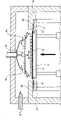
如图1和图2所示,本实施方式的断裂装置1用于使粘贴在晶片11背面的膜状粘接剂10在粘贴于保护带13的状态下断裂,所述保护带13安装在环状框架12的开口部12a上。另外,该断裂装置1至少包括:保持环状框架12的框架保持构件2;扩展保护带13的扩展构件3;使该扩展构件3和框架保持构件2的保持面相对定位的进退构件4;以及用于冷却膜状粘接剂10的冷却构件6,并且,该断裂装置1设置有对晶片11的表面进行鼓风的鼓风构件5。As shown in FIGS. 1 and 2 , the breaking device 1 of the present embodiment is used to break the film adhesive 10 attached to the back of the
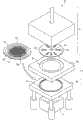
作为利用该断裂装置1进行断裂的对象的膜状粘接剂10是在安装或层叠半导体芯片时使用的部件,例如可以举出芯片焊接膜和芯片贴附膜等。此外,如图3所示,这些膜状粘接剂10通常设计成外径比晶片11的外径大,这些膜状粘接剂10的一部分从晶片11探出。另一方面,在晶片11的表面上呈矩阵状地形成有多个器件14,使膜状粘接剂10沿着划分这些器件14的格子状的间隔道15断裂。The film adhesive 10 to be broken by the breaking device 1 is a member used when mounting or laminating semiconductor chips, and examples thereof include die-bonding films and die-attach films. In addition, as shown in FIG. 3 , these
此外,本实施方式的断裂装置1的框架保持构件2具有由例如SUS(不锈钢)等金属材料构成的板状的保持部件2a、2b。在这一对保持部件2a、2b的中央部上,形成有直径与环状框架12的开口部12a大致相同的开口。另外,环状框架12以开口部12a与保持部件2a、2b的开口对齐的方式配置在保持部件2a和保持部件2b之间,通过利用保持部件2a、2b夹持环状框架12来保持环状框架12。该情况下,保持部件2a、2b各自的开口周围的面作为环状框架12的保持面发挥作用。Furthermore, the
另外,在图1所示的断裂装置1中,构成为利用保持部件2a和保持部件2b夹持环状框架12的结构,但是本发明并不限定于此,例如,也可以构成为利用夹紧器等固定部件将环状框架12固定在保持部件2a上的结构。该情况下,保持部件2a的开口的周围的面作为保持面发挥作用。In addition, in the breaking device 1 shown in FIG. 1, the ring-shaped
另一方面,扩展构件3作用于保护带13的晶片粘贴区域以使保护带13扩展,并具有圆形的推压面,所述保护带13安装在保持于上述框架保持构件2的环状框架12上。该推压面的直径比保持部件2a、2b的开口要小,该推压面构成为能够贯穿插入这些开口内。此外,扩展构件3在不作用于保护带13的待机状态时,配置在例如比保持部件2a的保持面靠下方的位置等那样的、不与保护带13接触的位置(以下称为待机位置)。另外,关于扩展构件3,也可以在推压面的外周部形成环状槽,并沿着该环状槽以能够自由旋转的方式配设多个扩展辅助辊。如果设置这样的扩展辅助辊,则能够减小在扩展保护带13时产生的摩擦阻力,能够均等地作用拉伸力。On the other hand, the
此外,进退构件4是使扩展构件3从待机位置定位到使保护带13扩展的扩展位置的构件,进退构件4可以使用例如伺服电动机等。在图1所示的断裂装置1中,进退构件4与扩展构件3的下部连接,使扩展构件3从比保持部件2a的保持面靠下方的待机位置移动至比保持面靠上方的扩展位置。另外,本发明的断裂装置并不限定于图1所示的使扩展构件3移动的结构,例如也可以构成为:将由空气活塞机构等构成的进退构件与框架保持构件2连接,并将扩展构件3的位置固定,通过移动框架保持构件2,来使保持部件2a的保持面与扩展构件3之间的位置关系成为待机位置或扩展位置。In addition, the forward and
另外,本实施方式的断裂装置1包括鼓风构件5,该鼓风构件5至少在扩展构件3定位于扩展位置时,向粘贴在正被扩展的保护带13上的晶片11进行鼓风。在该鼓风构件5中,在晶片11的正上方区域内设置有1个或多个空气喷射口5a。另外,从该空气喷射口5a向晶片11以使空气从晶片11的内侧流向外侧的方式喷射空气。通过该空气的流动,能够防止从晶片11探出的膜状粘接剂10的探出部分断裂而产生的碎片飞溅并附着到晶片11的表面上。In addition, the breaking device 1 of the present embodiment includes an
另外,在本实施方式的断裂装置1中,通过在晶片11的接近探出部分的边缘部的正上方区域配置多个空气喷射口5a,能够进一步提高防止碎片附着到晶片11上的效果。此外,除了在晶片11的边缘部的正上方区域之外,通过在晶片11的中心部的正上方区域也配置空气喷射口5a,还能够防止膜状粘接剂10沿间隔道15断裂时产生的灰尘等的附着。In addition, in the breaker 1 of the present embodiment, the effect of preventing debris from adhering to the
另外,在该断裂装置1中,也可以使空气喷射口5a的至少一个能够沿晶片11的半径方向移动。由此,能够容易地改变鼓风位置,所以能够应对各种尺寸的晶片11。In addition, in this breaking device 1 , at least one of the
在本实施方式的断裂装置1中,如图2所示,也可以将上述框架保持构件2、扩展构件3、进退构件4以及鼓风构件5用外壳7包围起来,该情况下,通过利用冷却构件6对外壳7内进行冷却,能够使膜状粘接剂10冷却。此时,外壳7例如可以构成为:其具有上方开口的长方体状的壳体7a、和以能够通过铰链自由开闭的方式将该壳体7a的上方开口部封闭起来的箱状的盖体7a,在壳体7a的一部分以能够自由开闭的方式设置有用于取出和放入环状框架12等的闸门机构7c。In the breaking device 1 of the present embodiment, as shown in FIG. 2 , the above-mentioned
此外,冷却构件6只要能够将外壳7内的温度冷却至大约-10~0℃即可,冷却构件6例如可以构成为:从冷却单元(cooler unit)等冷却气体供给装置经配管向外壳7内导入冷气,并且从设置于外壳7的排气口将内部的气体排出。In addition, the cooling
这样,在本实施方式的断裂装置1中,在使膜状粘接剂10断裂时,由于设置有从晶片11的内侧向外侧鼓风的鼓风构件5,所以能够防止膜状粘接剂10的探出部分断裂而产生的碎片飞溅并附着到晶片11的表面。In this way, in the breaking device 1 of the present embodiment, when the
接下来,对上述断裂装置1的动作、即、使用断裂装置1使膜状粘接剂10断裂的方法进行说明。图4~图7是按照工序顺序对利用本实施方式的断裂装置1使膜状粘接剂10断裂的方法进行表示的剖视图。在利用本实施方式的断裂装置1使膜状粘接剂10断裂的情况下,首先,如图4所示,在环状框架12的开口部12a上经保护带13支撑有在背面粘贴了膜状粘接剂10的晶片11,将该环状框架12载置到框架保持构件2的保持部件2a上。此时的晶片11可以是在切割后被分割成了一个个芯片的状态,也可以是利用激光在间隔道上形成了变质层的状态。Next, the operation of the breaking device 1 , that is, a method for breaking the
接下来,如图5所示,向外壳7内导入冷气,使膜状粘接剂10冷却,并且通过空气活塞机构等使保持部件2a上升,利用保持部件2a和保持部件2b夹持环状框架12。另外,在图5中,表示了通过使保持部件2a上升来形成夹持状态的情况,但是本发明并不限定于此,也可以通过使保持部件2b下降来夹持环状框架12。Next, as shown in FIG. 5 , cold air is introduced into the casing 7 to cool the
接下来,如图6所示,通过进退构件4,使扩展构件3从待机位置上升,并以预定的速度移动至比保持部件2a的保持面靠上方的扩展位置。由此,安装在环状框架12上的保护带13的晶片粘贴区域被顶起。此时,保护带13受到来自扩展构件3的外力而呈放射线状地扩展,由于保护带13的凝固点低,所以即使在大约-10~0℃的温度条件下也不会硬化。另一方面,在粘贴于保护带13上的膜状粘接剂10上也作用有拉伸力,但是,由于膜状粘接剂10被冷却而变硬,所以膜状粘接剂10沿着间隔道断裂而不是被扩展。Next, as shown in FIG. 6 , the
另外,在晶片11处于未分割、并且利用激光等在间隔道处形成了变质层的状态的情况下,当扩展保护带13时,拉伸力还作用于晶片11。由此,晶片11也与膜状粘接剂10一起沿着形成有变质层的位置、即间隔道断裂。In addition, when the
另外,在本实施方式的断裂载置1中,在上述的保护带13的扩展时,从鼓风构件5的空气喷射口5a向晶片11的表面喷射空气,进行鼓风。此时,空气从晶片11的内侧向外侧流动。由此,在扩展了保护带13时,即使膜状粘接剂10的从晶片11探出的探出部分发生断裂,也能够防止其碎片向晶片11的方向飞溅。Moreover, in fracture mounting 1 according to the present embodiment, air is blown by blowing air from
另外,关于上述鼓风,如图6所示,当从晶片11的边缘部的正上方区域喷射空气时,能够可靠地防止因探出部分的断裂而产生的碎片附着在晶片11上,另外,通过从晶片11的中心部的正上方区域喷射空气,还能够防止因沿着间隔道的通常位置处的断裂而产生的灰尘等的附着。In addition, regarding the above-mentioned blowing, as shown in FIG. 6, when the air is sprayed from the area directly above the edge of the
在膜状粘接剂10的断裂完成之后,如图7所示,使鼓风终止,利用进退构件4使扩展构件3下降至待机位置,并且使保持部件2a下降至预定位置。然后,结束外壳7内的冷却,将环状框架12取出。After the breaking of the
如上所述,在本实施方式的断裂装置1中,由于设置有对晶片11的表面进行鼓风的鼓风构件5,在使膜状粘接剂10断裂时,鼓风构件5以使空气从晶片11的内侧向外侧流动的方式进行鼓风,因此,即使膜状粘接剂10的探出部分断裂,也能够防止其碎片飞溅并附着到晶片11的表面上。由此,即使在使膜状粘接剂10在冷却的同时断裂的情况下,也能够抑制因异物附着在晶片11的表面而引起的不良情况的产生。其结果为,能够使膜状粘接剂10可靠地断裂,而不会使成品率降低。As described above, in the breaking device 1 of this embodiment, since the blowing
接下来,对本发明的第二实施方式的断裂装置进行说明。图8是表示本实施方式的断裂装置的结构的分解立体图。另外,在图8所示的断裂装置21中,对于与图1所示的断裂装置1的结构要素相同的部分标以相同标号,并省略其详细的说明。Next, a breaking device according to a second embodiment of the present invention will be described. Fig. 8 is an exploded perspective view showing the structure of the breaking device according to the present embodiment. In addition, in the
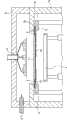
关于本实施方式的断裂装置21,在框架保持构件2的保持部件2b的开口处设置有止推部件8,除了该止推部件8以外,其余结构与上述第一实施方式的断裂装置1相同。在扩展构件3或保持部件2a的保持面定位于扩展位置时、即、在保护带13被扩展了时候,本实施方式的断裂装置21的止推部件8对膜状粘接剂10的从晶片11探出的部分进行止挡。The breaking
另外,本发明并不限定于如图8所示地在保持部件2b的开口处设置止推部件8的结构,止推部件8只要设置在能够对膜状粘接剂10的探出部分进行止挡的位置即可。例如,在像利用固定部件将框架12固定在保持部件2a上的情况那样的没有保持部件2b的结构的装置中,也可以单独设置止推部件8。In addition, the present invention is not limited to the structure in which the
此外,本实施方式的断裂装置21的止推部件8的材质优选为这样的材料:即使在-10~0℃的温度条件下仍具有挠性、而且在与膜状粘接剂10之间不会发生粘贴,可以举出例如橡胶和树脂等,特别优选梨皮面的聚氨酯材料。另外,优选的是,止推部件8在与膜状粘接剂10接触的面上形成有凹凸,由此,能够提高止推部件8与膜状粘接剂10之间的剥离性。In addition, the material of the
这样,在本实施方式的断裂装置21中,除了设置有鼓风构件5之外,还设置有对膜状粘接剂10的从晶片11探出的部分进行止挡的止推部件8,因此能够可靠地防止因膜状粘接剂10的探出部分的断裂而产生的碎片的飞溅。In this way, in the
接下来,对上述断裂装置21的动作、即、使用断裂装置21使膜状粘接剂10断裂的方法进行说明。图9~图12是按照工序顺序对利用本实施方式的断裂装置21使膜状粘接剂10断裂的方法进行表示的剖视图。在利用本实施方式的断裂装置21使膜状粘接剂10断裂的情况下,首先,如图9所示,在环状框架12的开口部12a处经保护带13支撑有在背面粘贴了膜状粘接剂10的晶片11,将该环状框架12载置到框架保持构件2的保持部件2a上。Next, the operation of the breaking
接下来,如图10所示,向外壳7内导入冷气,使膜状粘接剂10冷却,并且通过空气活塞机构等使保持部件2a上升,利用保持部件2a和保持部件2b夹持环状框架12。此时,膜状粘接剂10的探出部分与止推部件8接触,该探出部分成为被保护带13与止推部件8夹住的状态。Next, as shown in FIG. 10 , cool air is introduced into the casing 7 to cool the
接下来,如图11所示,通过进退构件,使扩展构件3从待机位置上升,并以预定的速度移动至比保持部件2a的保持面靠上方的扩展位置。由此,安装在环状框架12上的保护带13的晶片粘贴区域被顶起,因此,保护带13呈放射线状地扩展,膜状粘接剂10断裂。此外,由于此时膜状粘接剂10的探出部分被止推部件8止挡,所以即使在探出部分发生了断裂的情况下,也能够防止碎片的飞溅。Next, as shown in FIG. 11 , the
另外,在本实施方式的断裂装置21中,也与上述第一实施方式一样,在扩展构件3定位在了扩展位置时,通过鼓风构件5对晶片11的表面从内侧向外侧进行鼓风。由此,即使在未被止推部件8完全压住的部分飞溅出细小的碎片,也能够防止碎片附着在晶片11的表面上。Also in the
接下来,如图12所示,使鼓风终止,利用进退构件4使扩展构件3下降至待机位置,并且利用空气活塞机构等使保持部件2a也下降至预定位置。由此,解除止推部件8进行的止挡。然后,使外壳7内的冷却结束,将环状框架12取出。Next, as shown in FIG. 12 , the air blowing is terminated, the
如上所述,在本实施方式的断裂装置21中,在扩展保护带13时,在利用鼓风构件5向晶片11的表面进行鼓风的基础上,利用止推部件8对膜状粘接剂10的探出部分进行止挡,因此能够可靠地防止在膜状粘接剂10的探出部分产生的碎片的飞溅。由此,能够大幅度地减少因异物附着在晶片11表面上而引起的不良情况的产生。As described above, in the
另外,本实施方式的断裂装置21的除上述以外的其它结构和效果与上述第一实施方式的断裂装置1相同。In addition, the structure and effects other than the above of the breaking
Claims (6)
Translated fromChineseApplications Claiming Priority (3)
| Application Number | Priority Date | Filing Date | Title |
|---|---|---|---|
| JP2008122868 | 2008-05-09 | ||
| JP2008-122868 | 2008-05-09 | ||
| JP2008122868AJP2009272503A (en) | 2008-05-09 | 2008-05-09 | Breaking device and breaking method for filmy adhesive |
Publications (2)
| Publication Number | Publication Date |
|---|---|
| CN101577217Atrue CN101577217A (en) | 2009-11-11 |
| CN101577217B CN101577217B (en) | 2013-02-27 |
Family
ID=41272108
Family Applications (1)
| Application Number | Title | Priority Date | Filing Date |
|---|---|---|---|
| CN 200910135065ActiveCN101577217B (en) | 2008-05-09 | 2009-04-22 | Breaking device and breaking method of film adhesive |
Country Status (2)
| Country | Link |
|---|---|
| JP (1) | JP2009272503A (en) |
| CN (1) | CN101577217B (en) |
Cited By (7)
| Publication number | Priority date | Publication date | Assignee | Title |
|---|---|---|---|---|
| CN104425334A (en)* | 2013-09-09 | 2015-03-18 | 株式会社东芝 | Manufacturing method of semiconductor apparatus and semiconductor manufacturing apparatus |
| CN105321865A (en)* | 2014-06-13 | 2016-02-10 | 株式会社迪思科 | Tape expanding apparatus |
| CN106024671A (en)* | 2015-03-25 | 2016-10-12 | 株式会社迪思科 | Extension apparatus |
| CN107275256A (en)* | 2016-04-01 | 2017-10-20 | 株式会社迪思科 | Expanding unit |
| CN107452609A (en)* | 2016-05-11 | 2017-12-08 | 株式会社迪思科 | The processing method of chip |
| CN108630592A (en)* | 2017-03-24 | 2018-10-09 | 株式会社迪思科 | Sheet material expanding unit |
| CN111063648A (en)* | 2019-11-29 | 2020-04-24 | 力成科技(苏州)有限公司 | Non-adhesion separation process for wafer adhesive film |
Families Citing this family (13)
| Publication number | Priority date | Publication date | Assignee | Title |
|---|---|---|---|---|
| JP5648512B2 (en)* | 2011-02-08 | 2015-01-07 | トヨタ自動車株式会社 | Expanding method, expanding device, adhesive sheet |
| JP5939451B2 (en)* | 2011-02-18 | 2016-06-22 | 株式会社東京精密 | Work dividing apparatus and work dividing method |
| JP2011119767A (en)* | 2011-03-07 | 2011-06-16 | Sony Chemical & Information Device Corp | Method for dicing wafer, method for mounting, method for manufacturing chip with adhesive layer, and mounted body |
| JP5992277B2 (en) | 2012-09-20 | 2016-09-14 | 株式会社ディスコ | Processing method |
| JP6047353B2 (en) | 2012-09-20 | 2016-12-21 | 株式会社ディスコ | Processing method |
| JP5977633B2 (en)* | 2012-09-20 | 2016-08-24 | 株式会社ディスコ | Processing method |
| JP6320198B2 (en) | 2014-06-27 | 2018-05-09 | 株式会社ディスコ | Tape expansion unit |
| JP6270642B2 (en)* | 2014-06-27 | 2018-01-31 | 株式会社ディスコ | Tape expansion unit |
| JP6425435B2 (en)* | 2014-07-01 | 2018-11-21 | 株式会社ディスコ | Tip spacing maintenance device |
| JP6041065B2 (en)* | 2016-05-16 | 2016-12-07 | 株式会社東京精密 | Work dividing device |
| JP6376363B2 (en)* | 2016-11-10 | 2018-08-22 | 株式会社東京精密 | Work dividing device |
| KR102563929B1 (en) | 2018-03-09 | 2023-08-04 | 삼성전자주식회사 | Method of singulating semiconductor die and method of fabricating semiconductor package |
| JP7743525B2 (en)* | 2021-09-14 | 2025-09-24 | ヤマハ発動機株式会社 | Expanding Device |
Family Cites Families (7)
| Publication number | Priority date | Publication date | Assignee | Title |
|---|---|---|---|---|
| JP4137471B2 (en)* | 2002-03-04 | 2008-08-20 | 東京エレクトロン株式会社 | Dicing method, integrated circuit chip inspection method, and substrate holding apparatus |
| JP4503429B2 (en)* | 2004-02-10 | 2010-07-14 | リンテック株式会社 | Manufacturing method of semiconductor device |
| JP2006049591A (en)* | 2004-08-05 | 2006-02-16 | Disco Abrasive Syst Ltd | Method and apparatus for rupturing adhesive film adhered to wafer |
| JP4744957B2 (en)* | 2005-07-13 | 2011-08-10 | 株式会社ディスコ | Breaker for adhesive film mounted on wafer |
| JP2007067278A (en)* | 2005-09-01 | 2007-03-15 | Tokyo Seimitsu Co Ltd | Expanding method and expanding apparatus |
| JP4851795B2 (en)* | 2006-01-13 | 2012-01-11 | 株式会社ディスコ | Wafer divider |
| JP2007242787A (en)* | 2006-03-07 | 2007-09-20 | Disco Abrasive Syst Ltd | Wafer division method |
- 2008
- 2008-05-09JPJP2008122868Apatent/JP2009272503A/enactivePending
- 2009
- 2009-04-22CNCN 200910135065patent/CN101577217B/enactiveActive
Cited By (12)
| Publication number | Priority date | Publication date | Assignee | Title |
|---|---|---|---|---|
| CN104425334A (en)* | 2013-09-09 | 2015-03-18 | 株式会社东芝 | Manufacturing method of semiconductor apparatus and semiconductor manufacturing apparatus |
| CN104425334B (en)* | 2013-09-09 | 2018-11-13 | 东芝存储器株式会社 | The manufacturing method and semiconductor manufacturing apparatus of semiconductor device |
| CN105321865A (en)* | 2014-06-13 | 2016-02-10 | 株式会社迪思科 | Tape expanding apparatus |
| CN106024671A (en)* | 2015-03-25 | 2016-10-12 | 株式会社迪思科 | Extension apparatus |
| CN106024671B (en)* | 2015-03-25 | 2021-03-05 | 株式会社迪思科 | Expansion device |
| CN107275256A (en)* | 2016-04-01 | 2017-10-20 | 株式会社迪思科 | Expanding unit |
| CN107275256B (en)* | 2016-04-01 | 2022-02-22 | 株式会社迪思科 | Expansion device |
| CN107452609A (en)* | 2016-05-11 | 2017-12-08 | 株式会社迪思科 | The processing method of chip |
| CN107452609B (en)* | 2016-05-11 | 2023-04-25 | 株式会社迪思科 | Wafer processing method |
| CN108630592A (en)* | 2017-03-24 | 2018-10-09 | 株式会社迪思科 | Sheet material expanding unit |
| CN108630592B (en)* | 2017-03-24 | 2023-07-07 | 株式会社迪思科 | Sheet Expansion Device |
| CN111063648A (en)* | 2019-11-29 | 2020-04-24 | 力成科技(苏州)有限公司 | Non-adhesion separation process for wafer adhesive film |
Also Published As
| Publication number | Publication date |
|---|---|
| JP2009272503A (en) | 2009-11-19 |
| CN101577217B (en) | 2013-02-27 |
Similar Documents
| Publication | Publication Date | Title |
|---|---|---|
| CN101577217B (en) | Breaking device and breaking method of film adhesive | |
| JP5207455B2 (en) | Film adhesive breaking apparatus and breaking method | |
| CN100452287C (en) | Method and apparatus for dividing an adhesive film mounted on a wafer | |
| EP2038923B1 (en) | Method for fabricating semiconductor chips | |
| US20060130974A1 (en) | System for attaching semiconductor components to substrates | |
| JP4744957B2 (en) | Breaker for adhesive film mounted on wafer | |
| JP2007027562A (en) | Breaking method of adhesive film attached to wafer | |
| JP2010135356A (en) | Dicing method of wafer | |
| JP4324788B2 (en) | Wafer mounter | |
| JP4927582B2 (en) | Breaking method of adhesive film mounted on backside of wafer | |
| JP5636266B2 (en) | Workpiece processing method and dicing tape | |
| JP2006332078A (en) | Manufacturing method of semiconductor chip | |
| JP4971869B2 (en) | Adhesive film breaker | |
| JP6298699B2 (en) | Wafer processing method | |
| JP2000164535A (en) | Laser processing equipment | |
| KR100567040B1 (en) | Method and apparatus for machining substrate | |
| JP2012104644A (en) | Wafer cutting method and wafer cutting device | |
| KR100675001B1 (en) | Wafer dicing method and die manufactured using the method | |
| JP2004031844A (en) | Method of manufacturing semiconductor chip and manufacturing apparatus for semiconductor chip | |
| JP2000299329A (en) | Manufacturing apparatus and manufacturing method for resin package type semiconductor device | |
| JP2007180252A (en) | Manufacturing method of semiconductor device | |
| JP7629790B2 (en) | Cleaning tool and method for cleaning cover member | |
| TWI251899B (en) | Wafer dicing process for die free control | |
| JP2000021915A (en) | Semiconductor device and manufacture of semiconductor device | |
| JP2001267342A (en) | Method of manufacturing semiconductor device |
Legal Events
| Date | Code | Title | Description |
|---|---|---|---|
| C06 | Publication | ||
| PB01 | Publication | ||
| C10 | Entry into substantive examination | ||
| SE01 | Entry into force of request for substantive examination | ||
| C14 | Grant of patent or utility model | ||
| GR01 | Patent grant |