CN101577089B - Display apparatus and method of driving same - Google Patents
Display apparatus and method of driving sameDownload PDFInfo
- Publication number
- CN101577089B CN101577089BCN2009101411170ACN200910141117ACN101577089BCN 101577089 BCN101577089 BCN 101577089BCN 2009101411170 ACN2009101411170 ACN 2009101411170ACN 200910141117 ACN200910141117 ACN 200910141117ACN 101577089 BCN101577089 BCN 101577089B
- Authority
- CN
- China
- Prior art keywords
- potential
- signal
- source
- transistor
- driving transistor
- Prior art date
- Legal status (The legal status is an assumption and is not a legal conclusion. Google has not performed a legal analysis and makes no representation as to the accuracy of the status listed.)
- Active
Links
Images


Classifications
- G—PHYSICS
- G09—EDUCATION; CRYPTOGRAPHY; DISPLAY; ADVERTISING; SEALS
- G09G—ARRANGEMENTS OR CIRCUITS FOR CONTROL OF INDICATING DEVICES USING STATIC MEANS TO PRESENT VARIABLE INFORMATION
- G09G3/00—Control arrangements or circuits, of interest only in connection with visual indicators other than cathode-ray tubes
- G09G3/20—Control arrangements or circuits, of interest only in connection with visual indicators other than cathode-ray tubes for presentation of an assembly of a number of characters, e.g. a page, by composing the assembly by combination of individual elements arranged in a matrix no fixed position being assigned to or needed to be assigned to the individual characters or partial characters
- G09G3/22—Control arrangements or circuits, of interest only in connection with visual indicators other than cathode-ray tubes for presentation of an assembly of a number of characters, e.g. a page, by composing the assembly by combination of individual elements arranged in a matrix no fixed position being assigned to or needed to be assigned to the individual characters or partial characters using controlled light sources
- G09G3/30—Control arrangements or circuits, of interest only in connection with visual indicators other than cathode-ray tubes for presentation of an assembly of a number of characters, e.g. a page, by composing the assembly by combination of individual elements arranged in a matrix no fixed position being assigned to or needed to be assigned to the individual characters or partial characters using controlled light sources using electroluminescent panels
- G09G3/32—Control arrangements or circuits, of interest only in connection with visual indicators other than cathode-ray tubes for presentation of an assembly of a number of characters, e.g. a page, by composing the assembly by combination of individual elements arranged in a matrix no fixed position being assigned to or needed to be assigned to the individual characters or partial characters using controlled light sources using electroluminescent panels semiconductive, e.g. using light-emitting diodes [LED]
- G09G3/3208—Control arrangements or circuits, of interest only in connection with visual indicators other than cathode-ray tubes for presentation of an assembly of a number of characters, e.g. a page, by composing the assembly by combination of individual elements arranged in a matrix no fixed position being assigned to or needed to be assigned to the individual characters or partial characters using controlled light sources using electroluminescent panels semiconductive, e.g. using light-emitting diodes [LED] organic, e.g. using organic light-emitting diodes [OLED]
- G09G3/3225—Control arrangements or circuits, of interest only in connection with visual indicators other than cathode-ray tubes for presentation of an assembly of a number of characters, e.g. a page, by composing the assembly by combination of individual elements arranged in a matrix no fixed position being assigned to or needed to be assigned to the individual characters or partial characters using controlled light sources using electroluminescent panels semiconductive, e.g. using light-emitting diodes [LED] organic, e.g. using organic light-emitting diodes [OLED] using an active matrix
- G09G3/3233—Control arrangements or circuits, of interest only in connection with visual indicators other than cathode-ray tubes for presentation of an assembly of a number of characters, e.g. a page, by composing the assembly by combination of individual elements arranged in a matrix no fixed position being assigned to or needed to be assigned to the individual characters or partial characters using controlled light sources using electroluminescent panels semiconductive, e.g. using light-emitting diodes [LED] organic, e.g. using organic light-emitting diodes [OLED] using an active matrix with pixel circuitry controlling the current through the light-emitting element
- G—PHYSICS
- G09—EDUCATION; CRYPTOGRAPHY; DISPLAY; ADVERTISING; SEALS
- G09G—ARRANGEMENTS OR CIRCUITS FOR CONTROL OF INDICATING DEVICES USING STATIC MEANS TO PRESENT VARIABLE INFORMATION
- G09G3/00—Control arrangements or circuits, of interest only in connection with visual indicators other than cathode-ray tubes
- G09G3/20—Control arrangements or circuits, of interest only in connection with visual indicators other than cathode-ray tubes for presentation of an assembly of a number of characters, e.g. a page, by composing the assembly by combination of individual elements arranged in a matrix no fixed position being assigned to or needed to be assigned to the individual characters or partial characters
- G09G3/22—Control arrangements or circuits, of interest only in connection with visual indicators other than cathode-ray tubes for presentation of an assembly of a number of characters, e.g. a page, by composing the assembly by combination of individual elements arranged in a matrix no fixed position being assigned to or needed to be assigned to the individual characters or partial characters using controlled light sources
- G09G3/30—Control arrangements or circuits, of interest only in connection with visual indicators other than cathode-ray tubes for presentation of an assembly of a number of characters, e.g. a page, by composing the assembly by combination of individual elements arranged in a matrix no fixed position being assigned to or needed to be assigned to the individual characters or partial characters using controlled light sources using electroluminescent panels
- G—PHYSICS
- G09—EDUCATION; CRYPTOGRAPHY; DISPLAY; ADVERTISING; SEALS
- G09G—ARRANGEMENTS OR CIRCUITS FOR CONTROL OF INDICATING DEVICES USING STATIC MEANS TO PRESENT VARIABLE INFORMATION
- G09G3/00—Control arrangements or circuits, of interest only in connection with visual indicators other than cathode-ray tubes
- G09G3/20—Control arrangements or circuits, of interest only in connection with visual indicators other than cathode-ray tubes for presentation of an assembly of a number of characters, e.g. a page, by composing the assembly by combination of individual elements arranged in a matrix no fixed position being assigned to or needed to be assigned to the individual characters or partial characters
- G09G3/22—Control arrangements or circuits, of interest only in connection with visual indicators other than cathode-ray tubes for presentation of an assembly of a number of characters, e.g. a page, by composing the assembly by combination of individual elements arranged in a matrix no fixed position being assigned to or needed to be assigned to the individual characters or partial characters using controlled light sources
- G09G3/30—Control arrangements or circuits, of interest only in connection with visual indicators other than cathode-ray tubes for presentation of an assembly of a number of characters, e.g. a page, by composing the assembly by combination of individual elements arranged in a matrix no fixed position being assigned to or needed to be assigned to the individual characters or partial characters using controlled light sources using electroluminescent panels
- G09G3/32—Control arrangements or circuits, of interest only in connection with visual indicators other than cathode-ray tubes for presentation of an assembly of a number of characters, e.g. a page, by composing the assembly by combination of individual elements arranged in a matrix no fixed position being assigned to or needed to be assigned to the individual characters or partial characters using controlled light sources using electroluminescent panels semiconductive, e.g. using light-emitting diodes [LED]
- H—ELECTRICITY
- H05—ELECTRIC TECHNIQUES NOT OTHERWISE PROVIDED FOR
- H05B—ELECTRIC HEATING; ELECTRIC LIGHT SOURCES NOT OTHERWISE PROVIDED FOR; CIRCUIT ARRANGEMENTS FOR ELECTRIC LIGHT SOURCES, IN GENERAL
- H05B33/00—Electroluminescent light sources
- H05B33/12—Light sources with substantially two-dimensional radiating surfaces
- G—PHYSICS
- G09—EDUCATION; CRYPTOGRAPHY; DISPLAY; ADVERTISING; SEALS
- G09G—ARRANGEMENTS OR CIRCUITS FOR CONTROL OF INDICATING DEVICES USING STATIC MEANS TO PRESENT VARIABLE INFORMATION
- G09G2300/00—Aspects of the constitution of display devices
- G09G2300/08—Active matrix structure, i.e. with use of active elements, inclusive of non-linear two terminal elements, in the pixels together with light emitting or modulating elements
- G09G2300/0809—Several active elements per pixel in active matrix panels
- G09G2300/0819—Several active elements per pixel in active matrix panels used for counteracting undesired variations, e.g. feedback or autozeroing
- G—PHYSICS
- G09—EDUCATION; CRYPTOGRAPHY; DISPLAY; ADVERTISING; SEALS
- G09G—ARRANGEMENTS OR CIRCUITS FOR CONTROL OF INDICATING DEVICES USING STATIC MEANS TO PRESENT VARIABLE INFORMATION
- G09G2300/00—Aspects of the constitution of display devices
- G09G2300/08—Active matrix structure, i.e. with use of active elements, inclusive of non-linear two terminal elements, in the pixels together with light emitting or modulating elements
- G09G2300/0809—Several active elements per pixel in active matrix panels
- G09G2300/0842—Several active elements per pixel in active matrix panels forming a memory circuit, e.g. a dynamic memory with one capacitor
- G09G2300/0861—Several active elements per pixel in active matrix panels forming a memory circuit, e.g. a dynamic memory with one capacitor with additional control of the display period without amending the charge stored in a pixel memory, e.g. by means of additional select electrodes
- G09G2300/0866—Several active elements per pixel in active matrix panels forming a memory circuit, e.g. a dynamic memory with one capacitor with additional control of the display period without amending the charge stored in a pixel memory, e.g. by means of additional select electrodes by means of changes in the pixel supply voltage
- G—PHYSICS
- G09—EDUCATION; CRYPTOGRAPHY; DISPLAY; ADVERTISING; SEALS
- G09G—ARRANGEMENTS OR CIRCUITS FOR CONTROL OF INDICATING DEVICES USING STATIC MEANS TO PRESENT VARIABLE INFORMATION
- G09G2320/00—Control of display operating conditions
- G09G2320/04—Maintaining the quality of display appearance
- G09G2320/043—Preventing or counteracting the effects of ageing
Landscapes
- Engineering & Computer Science (AREA)
- Physics & Mathematics (AREA)
- Computer Hardware Design (AREA)
- General Physics & Mathematics (AREA)
- Theoretical Computer Science (AREA)
- Control Of Indicators Other Than Cathode Ray Tubes (AREA)
- Control Of El Displays (AREA)
- Electroluminescent Light Sources (AREA)
- Liquid Crystal (AREA)
Abstract
Translated fromChinese
Description
Translated fromChinese本申请是申请日为2007年5月22日、申请号为200710142109.9、发明名称为“显示设备和驱动该显示设备的方法”的发明专利申请的分案申请。This application is a divisional application of an invention patent application with a filing date of May 22, 2007, an application number of 200710142109.9, and an invention title of "Display Device and Method for Driving the Display Device".
相关申请的交叉引用Cross References to Related Applications
本发明包含于2006年5月22日向日本专利局提交的日本专利申请JP2006-141836相关的主题,在此通过引用的方式将其完整地包含在本申请中。The present invention contains subject matter related to Japanese Patent Application JP2006-141836 filed in the Japan Patent Office on May 22, 2006, which is hereby incorporated by reference in its entirety.
技术领域technical field
本发明涉及有源矩阵显示设备,其具有作为其像素的发光器件,并涉及驱动该有源矩阵显示设备的方法。The present invention relates to an active matrix display device having light emitting devices as pixels thereof and to a method of driving the active matrix display device.
背景技术Background technique
近年来,更多的努力用于研发用有机EL器件作为发光器件的平板自发射显示设备。有机EL器件是一种利用有机薄膜在电场下发光的现象的设备。由于有机EL器件能在10V或者更低的低电压下激发,因此其需要较低的能量。由于有机EL器件是自己能够发光的自发射器件,其不需要照明元件,因此可以重量轻、外形小。由于有机EL器件具有非常高的大约几微秒的值的响应速度,所以,在其显示运动图像时不会产生成图像滞后。In recent years, more efforts have been devoted to the development of flat-panel self-emission display devices using organic EL devices as light-emitting devices. An organic EL device is a device that utilizes the phenomenon that an organic thin film emits light under an electric field. Since the organic EL device can be excited at a low voltage of 10 V or less, it requires lower energy. Since the organic EL device is a self-emitting device capable of emitting light by itself, it does not require a lighting element, and thus can be light in weight and small in shape. Since the organic EL device has a very high response speed on the order of several microseconds, no image lag occurs when it displays a moving image.
在使用有机EL器件作为像素的平板自发射显示设备中,包括集成在各个像素中作为驱动元件的薄膜晶体管的有源矩阵显示设备发展尤其活跃。有源矩阵平板自发射显示设备在日本特许公开专利号2003-255856、2003-271095、2004-133240、2004-029791和2004-093682中公开。Among flat panel self-emission display devices using organic EL devices as pixels, active matrix display devices including thin film transistors integrated in individual pixels as driving elements are particularly actively developed. Active matrix flat panel self-emissive display devices are disclosed in Japanese Laid-Open Patent Nos. 2003-255856, 2003-271095, 2004-133240, 2004-029791 and 2004-093682.
发明内容Contents of the invention
在现有的有源矩阵平板自发射显示设备中,驱动发光器件的晶体管具有多种阈值电压和由制造过程变化导致的迁移率。另外,有机EL器件具有趋向于随时间变化的特性。驱动晶体管的这种特性变化和有机EL器件的特性变化不利地影响发光亮度。为了一致地控制在显示设备的整个屏幕上的发光亮度,有必要在像素电路中校正驱动晶体管和有机EL器件的上述特性变化。迄今为止,已提出了在每个像素上都具有校正功能的显示设备。然而,由于现有的具有校正功能的像素电路要求用于提供校正电位、切换晶体管、以及切换脉冲的互连,所以,现有的具有校正功能的像素电路的结构非常复杂。由于每个像素电路具有很多部件,所以,它们已阻碍了实现高清晰度显示的努力。In existing active-matrix flat-panel self-emitting display devices, the transistors driving the light-emitting devices have various threshold voltages and mobilities caused by manufacturing process variations. In addition, organic EL devices have characteristics that tend to change with time. Such characteristic variation of the driving transistor and characteristic variation of the organic EL device adversely affect light emission luminance. In order to uniformly control the luminance of light emission over the entire screen of the display device, it is necessary to correct the above-mentioned characteristic variation of the driving transistor and the organic EL device in the pixel circuit. So far, display devices having a correction function on each pixel have been proposed. However, since the conventional pixel circuit with correction function requires interconnection for providing correction potential, switching transistor, and switching pulse, the structure of the conventional pixel circuit with correction function is very complicated. Since each pixel circuit has many components, they have hindered efforts to achieve high definition displays.
期望提供用简化的像素电路来实现高清晰度显示的显示设备、以及驱动这样的显示设备的方法。It is desirable to provide a display device that realizes high-definition display with simplified pixel circuits, and a method of driving such a display device.
根据本发明的实施例,提供了一种显示设备,其包括像素阵列和被配置为驱动像素阵列的驱动器,该像素阵列具有作为行的扫描线、作为列的信号线、被置于扫描线和信号线的各个相交处的像素矩阵、以及沿像素的各行而布置的电源线,该驱动器具有:主扫描器,用于向扫描线连续地提供控制信号,以对像素的行执行逐行扫描(line-sequential scanning);电源扫描器,用于与逐行扫描同步地向电源线提供可选择性地在第一电位和第二电位之间切换的电源电压;以及信号选择器,用于与逐行扫描同步地向作为列的信号线提供用作视频信号的信号电位、以及参考电位,其中,每个像素包括发光器件、采样晶体管、驱动晶体管和保持电容器,采样晶体管具有栅极、源极和漏极,栅极连接到扫描线之一,源极和漏极中的任一个连接到信号线之一,而源极和漏极中的另一个连接到驱动晶体管的栅极,驱动晶体管具有源极和漏极,所述源极和漏极中的任一个连接到发光器件,而所述源极和漏极中的另一个连接到电源线之一,保持电容器连接在驱动晶体管的源极和栅极之间,其中,采样晶体管根据从扫描线提供的控制信号而呈现为导通,对从信号线提供的信号电位进行采样,并把采样的信号电位保持在保持电容器中,从在第一电位上的电源线向驱动晶体管提供电流,并且,根据保持在保持电容器中的信号电位而将驱动电流传递到发光器件,并且,当信号选择器在采样晶体管呈现为导通之后向信号线提供参考电位时,电源扫描器在第一电位和第二电位之间切换电源线,由此,在保持电容器中保持与驱动晶体管的阈值电压基本相对应的电压。According to an embodiment of the present invention, there is provided a display device including a pixel array and a driver configured to drive the pixel array, the pixel array has scan lines as rows, signal lines as columns, and a driver configured to drive the pixel array. pixel matrix at each intersection of signal lines, and power supply lines arranged along each row of pixels, the driver has: a main scanner for continuously supplying control signals to scanning lines to perform row-by-row scanning of rows of pixels ( line-sequential scanning); a power scanner for supplying a power supply line with a power supply voltage selectively switchable between a first potential and a second potential in synchronization with progressive scanning; and a signal selector for synchronizing with progressive scanning Row scanning synchronously supplies a signal potential used as a video signal and a reference potential to a signal line as a column, wherein each pixel includes a light emitting device, a sampling transistor, a driving transistor, and a holding capacitor, and the sampling transistor has a gate, a source, and a The drain and the gate are connected to one of the scanning lines, either one of the source and the drain is connected to one of the signal lines, and the other of the source and the drain is connected to the gate of the driving transistor, which has a source and a drain, either one of the source and the drain is connected to the light emitting device, and the other of the source and the drain is connected to one of the power supply lines, and a holding capacitor is connected between the source and the drain of the driving transistor. Between the gates, in which the sampling transistor is rendered conductive according to the control signal supplied from the scanning line, samples the signal potential supplied from the signal line, and holds the sampled signal potential in the holding capacitor, from the first The power supply line on the potential supplies current to the driving transistor, and delivers the driving current to the light emitting device according to the signal potential held in the holding capacitor, and, when the signal selector supplies the reference to the signal line after the sampling transistor is rendered conductive The power scanner switches the power supply line between the first potential and the second potential, thereby maintaining a voltage substantially corresponding to the threshold voltage of the driving transistor in the holding capacitor.
优选地,在采样晶体管呈现为导通之后的第一定时,信号选择器将信号线从参考电位切换到信号电位,主扫描器在第一定时后的第二定时停止向扫描线施加控制信号,由此,使采样晶体管呈现为非导通,并且,适当地设置第一定时和第二定时之间的周期,以针对驱动晶体管的迁移率,而在信号电位被保持在保持电容器中时校正信号电位。驱动器调整在从信号选择器提供的视频信号和从主扫描器提供的控制信号之间的相对相位差,以优化第一定时和第二定时之间的周期。信号选择器向从参考电位切换到信号电位的视频信号的上升沿施加梯度,以由此允许第一定时和第二定时之间的周期自动地跟随信号电位。当信号电位被保持电容器保持时,主扫描器停止向扫描线施加控制信号,因此,使采样晶体管呈现为非导通,以断开驱动晶体管的栅极与信号线的电连接,使得驱动晶体管的栅极电位与驱动晶体管的源极电位的变化相关联,以保持驱动晶体管的栅极和源极之间的电压恒定。Preferably, the signal selector switches the signal line from the reference potential to the signal potential at a first timing after the sampling transistor is turned on, and the main scanner stops applying the control signal to the scanning line at a second timing after the first timing, Thereby, the sampling transistor is rendered non-conductive, and the period between the first timing and the second timing is appropriately set to correct the signal while the signal potential is held in the holding capacitor with respect to the mobility of the driving transistor. potential. The driver adjusts a relative phase difference between the video signal supplied from the signal selector and the control signal supplied from the main scanner to optimize a period between the first timing and the second timing. The signal selector applies a gradient to the rising edge of the video signal switching from the reference potential to the signal potential to thereby allow the period between the first timing and the second timing to automatically follow the signal potential. When the signal potential is held by the hold capacitor, the main scanner stops applying the control signal to the scan line, so that the sampling transistor is rendered non-conductive to disconnect the electrical connection between the gate of the drive transistor and the signal line, so that the drive transistor The gate potential is correlated with the change in the source potential of the drive transistor to keep the voltage between the gate and source of the drive transistor constant.
根据本发明的实施例,还提供了一种显示设备,其包括像素阵列和被配置为驱动像素阵列的驱动器,该像素阵列具有作为行的扫描线、作为列的信号线、被置于扫描线和信号线的各个相交处的像素矩阵、以及沿像素的各行而布置的电源线,该驱动器具有:主扫描器,用于向扫描线连续地提供控制信号,以对像素的行执行逐行扫描;电源扫描器,用于与逐行扫描同步地向电源线提供可选择性地在第一电位和第二电位之间切换的电源电压;以及信号选择器,用于与逐行扫描同步地向作为列的信号线提供用作视频信号的信号电位、以及参考电位,其中,每个像素包括发光器件、采样晶体管、驱动晶体管和保持电容器,采样晶体管具有栅极、源极和漏极,栅极连接到扫描线之一,所述源极和漏极中的任一个连接到信号线之一,而所述源极和漏极中的另一个连接到驱动晶体管的栅极,驱动晶体管具有源极和漏极,所述源极和漏极中的任一个连接到发光器件,而所述源极和漏极中的另一个连接到电源线之一,保持电容器连接在驱动晶体管的源极和栅极之间,其中,采样晶体管根据从扫描线提供的控制信号而呈现为导通,对从信号线提供的信号电位进行采样,并把采样的信号电位保持在保持电容器中,从在第一电位上的电源线向驱动晶体管提供电流,并且,根据保持在保持电容器中的信号电位而将驱动电流传递到发光器件,在采样晶体管呈现为导通之后的第一定时,信号选择器将信号线从参考电位切换到信号电位,主扫描器在第一定时后的第二定时停止向扫描线施加控制信号,由此,使采样晶体管呈现为非导通,并且,适当地设置第一定时和第二定时之间的周期,以针对驱动晶体管的迁移率,而在信号电位被保持在保持电容器中时校正信号电位。According to an embodiment of the present invention, there is also provided a display device including a pixel array and a driver configured to drive the pixel array, the pixel array has scan lines as rows, signal lines as columns, and a pixel matrix at respective intersections of signal lines, and power supply lines arranged along respective rows of pixels, the driver has: a main scanner for continuously supplying control signals to scanning lines to perform row-by-row scanning of rows of pixels ; a power scanner for supplying a power supply voltage selectively switchable between a first potential and a second potential to a power supply line in synchronization with progressive scanning; and a signal selector for supplying a power supply voltage in synchronization with progressive scanning to A signal line serving as a column provides a signal potential used as a video signal, and a reference potential, wherein each pixel includes a light emitting device, a sampling transistor, a driving transistor, and a holding capacitor, the sampling transistor has a gate, a source, and a drain, and the gate connected to one of the scanning lines, either one of the source and drain is connected to one of the signal lines, and the other of the source and drain is connected to the gate of the driving transistor, which has a source and the drain, either one of the source and the drain is connected to the light emitting device, and the other of the source and the drain is connected to one of the power supply lines, and the holding capacitor is connected between the source and the gate of the driving transistor between electrodes, in which the sampling transistor is rendered conductive in accordance with the control signal supplied from the scanning line, samples the signal potential supplied from the signal line, and holds the sampled signal potential in the holding capacitor from the first potential The power supply line above supplies current to the driving transistor, and delivers the driving current to the light emitting device according to the signal potential held in the holding capacitor, and at the first timing after the sampling transistor is turned on, the signal selector switches the signal line from The reference potential is switched to the signal potential, the main scanner stops applying the control signal to the scanning line at the second timing after the first timing, thereby rendering the sampling transistor non-conductive, and setting the first timing and the second timing appropriately. The periods between are timed to correct the signal potential while the signal potential is held in the hold capacitor for the mobility of the drive transistor.
优选地,驱动器调整在从信号选择器提供的视频信号和从主扫描器提供的控制信号之间的相对相位差,以优化第一定时和第二定时之间的周期。信号选择器向在第一定时从参考电位切换到信号电位的视频信号的上升沿施加梯度,以由此允许第一定时和第二定时之间的周期自动地跟随信号电位。在信号电位被保持电容器保持的第二定时,主扫描器停止向扫描线施加控制信号,因此,使采样晶体管呈现为非导通,以断开驱动晶体管的栅极与信号线的电连接,使得驱动晶体管的栅极电位与驱动晶体管的源极电位的变化相关联,以保持驱动晶体管的栅极和源极之间的电压恒定。当信号选择器在采样晶体管呈现为导通之后向信号线提供参考电位时,电源扫描器在第一电位和第二电位之间切换电源线,由此,在保持电容器中保持与驱动晶体管的阈值电压相对应的电压。Preferably, the driver adjusts a relative phase difference between the video signal supplied from the signal selector and the control signal supplied from the main scanner to optimize a period between the first timing and the second timing. The signal selector applies a gradient to a rising edge of the video signal switched from the reference potential to the signal potential at the first timing, to thereby allow a period between the first timing and the second timing to automatically follow the signal potential. At the second timing at which the signal potential is held by the holding capacitor, the main scanner stops applying the control signal to the scanning line, thereby rendering the sampling transistor non-conductive to disconnect the electrical connection between the gate of the driving transistor and the signal line, so that The potential of the gate of the driving transistor is correlated with the variation of the potential of the source of the driving transistor to keep the voltage between the gate and the source of the driving transistor constant. When the signal selector supplies the reference potential to the signal line after the sampling transistor is rendered conductive, the power scanner switches the power supply line between the first potential and the second potential, whereby the threshold value of the driving transistor is held in the hold capacitor voltage corresponding to the voltage.
根据本发明的实施例的显示设备在每个像素中具有阈值电压校正功能、迁移率校正功能、以及自举功能。阈值电压校正功能校正驱动晶体管的阈值电压的变化。迁移率校正功能校正驱动晶体管的迁移率的变化。不论用作发光器件的有机EL器件的特性变化如何,在发光器件发光时保持电容器的自举操作在所有时间内都有效地将发光亮度保持为恒定的级别。具体地,即使有机EL器件的电流对电压特性随时间而变化,但由于驱动晶体管的栅极到源极电位通过被自举的保持电容器而保持恒定,所以,发光亮度仍然保持在恒定的级别。A display device according to an embodiment of the present invention has a threshold voltage correction function, a mobility correction function, and a bootstrap function in each pixel. The threshold voltage correction function corrects variations in the threshold voltage of the drive transistor. The mobility correction function corrects variations in the mobility of the drive transistor. The bootstrap operation of the holding capacitor is effective in maintaining the luminance of light emission at a constant level at all times when the light emitting device emits light regardless of the characteristic variation of the organic EL device used as the light emitting device. Specifically, even if the current versus voltage characteristic of the organic EL device varies with time, since the gate-to-source potential of the driving transistor is kept constant by the bootstrap holding capacitor, the luminance of light emission is maintained at a constant level.
为了把阈值电压校正功能、迁移率校正功能和自举功能合并到每一个像素中,作为切换脉冲而施加向每个像素提供的电源电压。通过作为切换脉冲施加的电源电压,不再要求用于校正阈值电压的开关晶体管、以及用于控制开关晶体管的栅极的扫描线。因此,像素内的部件数目和互连就大大减少,使减少像素面积以提供高清晰度显示成为可能。可以基于视频信号和采样脉冲的相位差,通过与视频信号电位的采样同时校正迁移率,来调整迁移率校正周期。此外,可以控制迁移率校正周期,以自动地跟随视频信号的电平。由于像素的部件数目比较小,所以,加到驱动晶体管的栅极上的任何寄生电容也比较小,使得可以可靠地自举保持电容器,由此改善校正有机EL器件的依赖于时间的变化。In order to incorporate a threshold voltage correction function, a mobility correction function, and a bootstrap function into each pixel, the power supply voltage supplied to each pixel is applied as a switching pulse. With the power supply voltage applied as a switching pulse, switching transistors for correcting threshold voltages, and scan lines for controlling the gates of the switching transistors are no longer required. As a result, the number of components and interconnections within a pixel are greatly reduced, making it possible to reduce the pixel area to provide high-definition displays. The mobility correction cycle can be adjusted by correcting the mobility simultaneously with the sampling of the potential of the video signal based on the phase difference between the video signal and the sampling pulse. In addition, the mobility correction period can be controlled to automatically follow the level of the video signal. Since the component count of the pixel is relatively small, any parasitic capacitance added to the gate of the drive transistor is also relatively small so that the holding capacitor can be reliably bootstrapped, thereby improving correction for time-dependent variations of the organic EL device.
根据本发明的实施例,在使用如有机EL器件的发光器件作为像素的有源矩阵显示设备中,每个像素都具有为驱动晶体管的阈值电压校正功能、迁移率校正功能、以及用来校正有机EL器件的依赖于时间的变化的功能(自举功能),从而允许显示设备可以显示高清晰度图像。由于迁移率校正周期可以根据视频信号电位而被自动设置,所以,不管显示图像的亮度和图案如何,都可以校正迁移率。现有的具有这些校正功能的像素电路由很多部件构成,具有较大的布局面积,并因此不适合于提供高清晰度显示。然而,根据本发明的一个实施例,由于作为切换脉冲而施加电源电压,所以,大大减少了像素的部件数目及其互连,使得减少像素布局面积成为可能。因此,根据本发明的实施例的显示设备可被提供为高质量、高清晰度平板显示单元。According to an embodiment of the present invention, in an active matrix display device using a light-emitting device such as an organic EL device as a pixel, each pixel has a threshold voltage correction function for a drive transistor, a mobility correction function, and a function for correcting the organic EL device. The function (bootstrap function) of the time-dependent change of the EL device, thereby allowing the display device to display high-definition images. Since the mobility correction cycle can be automatically set according to the video signal potential, the mobility can be corrected regardless of the brightness and pattern of the displayed image. Existing pixel circuits having these correction functions are composed of many components, have a large layout area, and are therefore not suitable for providing high-definition displays. However, according to an embodiment of the present invention, since a power supply voltage is applied as a switching pulse, the number of components of a pixel and their interconnections are greatly reduced, making it possible to reduce a layout area of a pixel. Therefore, a display device according to an embodiment of the present invention can be provided as a high-quality, high-definition flat panel display unit.
根据本发明的另一方面,提供了一种驱动具有像素阵列和被配置为驱动像素阵列的驱动器的显示设备的方法,所述像素阵列具有作为行的扫描线、作为列的信号线、被置于所述扫描线和所述信号线的各个相交处的像素矩阵、以及沿所述像素的各行而布置的电源线,所述驱动器具有:主扫描器,用于向所述扫描线连续地提供控制信号,以对所述像素的行执行逐行扫描;电源扫描器,用于与逐行扫描同步地向所述电源线提供可选择性地在第一电位和第二电位之间切换的电源电压;以及信号选择器,用于与逐行扫描同步地向作为列的所述信号线提供用作视频信号的信号电位、以及参考电位,每个所述像素包括发光器件、采样晶体管、驱动晶体管和保持电容器,所述采样晶体管具有栅极、源极和漏极,所述栅极连接到所述扫描线之一,所述源极和所述漏极中的任一个连接到所述信号线之一,而所述源极和所述漏极中的另一个连接到所述驱动晶体管的栅极,所述驱动晶体管具有源极和漏极,所述源极和所述漏极中的任一个连接到所述发光器件,而所述源极和所述漏极中的另一个连接到所述电源线之一,所述保持电容器连接在所述驱动晶体管的源极和栅极之间,所述方法包括以下步骤:根据从所述扫描线提供的控制信号而使所述采样晶体管呈现为导通,以对从所述信号线提供的信号电位进行采样,并把采样的信号电位保持在所述保持电容器中;从在所述第一电位上的电源线向所述驱动晶体管提供电流,并且,根据保持在所述保持电容器中的信号电位而将驱动电流传递到所述发光器件;在所述采样晶体管呈现为导通之后的第一定时,控制所述信号选择器将所述信号线从参考电位切换到信号电位;在所述第一定时后的第二定时,控制所述主扫描器停止向所述扫描线施加控制信号,由此,使所述采样晶体管呈现为非导通;以及适当地设置第一定时和第二定时之间的周期,以针对所述驱动晶体管的迁移率,而在信号电位被保持在所述保持电容器中时校正信号电位。According to another aspect of the present invention, there is provided a method of driving a display device having a pixel array having scanning lines as rows, signal lines as columns, and a driver configured to drive the pixel arrays. A pixel matrix at each intersection of the scanning line and the signal line, and a power supply line arranged along each row of the pixel, the driver has: a main scanner for continuously supplying the scanning line a control signal to perform progressive scanning on the rows of the pixels; a power scanner for supplying power selectively switchable between a first potential and a second potential to the power supply line in synchronization with the progressive scanning a voltage; and a signal selector for supplying a signal potential serving as a video signal and a reference potential to said signal line as a column in synchronization with progressive scanning, each of said pixels including a light emitting device, a sampling transistor, a driving transistor and a hold capacitor, the sampling transistor has a gate, a source, and a drain, the gate is connected to one of the scan lines, and either one of the source and the drain is connected to the signal line One of the source and the drain is connected to the gate of the driving transistor, the driving transistor has a source and a drain, and any of the source and the drain one is connected to the light emitting device and the other of the source and the drain is connected to one of the power supply lines, the holding capacitor is connected between the source and the gate of the driving transistor, The method includes the steps of rendering the sampling transistor conductive according to a control signal supplied from the scanning line to sample a signal potential supplied from the signal line, and maintaining the sampled signal potential at In the hold capacitor; supply current from a power supply line at the first potential to the drive transistor, and deliver drive current to the light emitting device according to the signal potential held in the hold capacitor; At a first timing after the sampling transistor is turned on, the signal selector is controlled to switch the signal line from a reference potential to a signal potential; at a second timing after the first timing, control the main scanning The device stops applying the control signal to the scan line, thereby rendering the sampling transistor non-conductive; and appropriately setting the period between the first timing and the second timing to target the mobility of the driving transistor , and the signal potential is corrected while the signal potential is held in the holding capacitor.
附图说明Description of drawings
图1为一般像素结构的电路图;FIG. 1 is a circuit diagram of a general pixel structure;
图2为图1所示的像素电路的操作序列的时序图;FIG. 2 is a timing diagram of an operation sequence of the pixel circuit shown in FIG. 1;
图3A为根据本发明一个实施例的显示设备的总体布置的框图;3A is a block diagram of a general arrangement of a display device according to one embodiment of the present invention;
图3B为根据本发明一个实施例的显示设备的像素电路的电路图;3B is a circuit diagram of a pixel circuit of a display device according to an embodiment of the present invention;
图4A为图3B所示的像素电路的操作序列的时序图;FIG. 4A is a timing diagram of the operation sequence of the pixel circuit shown in FIG. 3B;
图4B为说明图3B所示的像素电路的操作方式的电路图;4B is a circuit diagram illustrating the operation of the pixel circuit shown in FIG. 3B;
图4C为说明图3B所示的像素电路的操作方式的电路图;4C is a circuit diagram illustrating the operation of the pixel circuit shown in FIG. 3B;
图4D为说明图3B所示的像素电路的操作方式的电路图;4D is a circuit diagram illustrating the operation of the pixel circuit shown in FIG. 3B;
图4E为说明图3B所示的像素电路的操作方式的电路图;FIG. 4E is a circuit diagram illustrating the mode of operation of the pixel circuit shown in FIG. 3B;
图4F为说明图3B所示的像素电路的操作方式的电路图;FIG. 4F is a circuit diagram illustrating the operation of the pixel circuit shown in FIG. 3B;
图4G为说明图3B所示的像素电路的操作方式的电路图;FIG. 4G is a circuit diagram illustrating the operation of the pixel circuit shown in FIG. 3B;
图5为示出驱动晶体管的电流对电压特性的图;5 is a graph showing current versus voltage characteristics of a driving transistor;
图6A为示出不同的驱动晶体管的电流对电压特性的图;FIG. 6A is a graph showing current versus voltage characteristics of different drive transistors;
图6B为说明图3B所示的像素电路的操作方式的电路图;FIG. 6B is a circuit diagram illustrating the mode of operation of the pixel circuit shown in FIG. 3B;
图6C为说明图3B所示的像素电路的操作方式的波形图;6C is a waveform diagram illustrating the operation of the pixel circuit shown in FIG. 3B;
图6D为示出用于说明图3B所示的像素电路的操作方式的电流对电压特性的图;FIG. 6D is a graph showing current versus voltage characteristics for explaining the manner of operation of the pixel circuit shown in FIG. 3B;
图7A为示出发光器件的电流对电压特性的图;7A is a graph showing current versus voltage characteristics of a light emitting device;
图7B为示出驱动晶体管的自举(bootstrap)操作的波形图;7B is a waveform diagram illustrating a bootstrap operation of a drive transistor;
图7C为说明图3B所示的像素电路的操作方式的电路图;7C is a circuit diagram illustrating the operation of the pixel circuit shown in FIG. 3B;
图8为根据本发明的一个实施例的显示设备的像素电路的电路图;8 is a circuit diagram of a pixel circuit of a display device according to an embodiment of the present invention;
图9A到9G为示出电子单元显示设备的具体示例的图;和9A to 9G are diagrams showing specific examples of electronic unit display devices; and
图10为模块的平面图。Figure 10 is a plan view of the module.
具体实施方式Detailed ways
为了更容易地理解本发明和清楚其背景,下面开始结合图1而描述显示设备的一般结构。图1为示出一般的显示设备的像素的电路图。如图1所示,该像素电路具有设置在互相垂直延伸的扫描线1E和信号线1F相交处的采样晶体管1A。采样晶体管1A为N型晶体管,其具有连接到扫描线1E的栅极和连接到信号线1F的漏极。采样晶体管1A具有连接到保持电容器器1C的电极和驱动晶体管1B的栅极的源极。驱动晶体管1B为N型晶体管,其具有与电源线1G连接的漏极、以及与发光器件1D的阳极连接的源极。保持电容器1C的另一电极和发光器件1D的阴极与地线1H连接。In order to understand the present invention more easily and clarify its background, the general structure of a display device will be described below in conjunction with FIG. 1 . FIG. 1 is a circuit diagram showing a pixel of a general display device. As shown in FIG. 1, the pixel circuit has a sampling transistor 1A provided at the intersection of a scanning line 1E and a signal line 1F extending perpendicularly to each other. The sampling transistor 1A is an N-type transistor having a gate connected to the scan line 1E and a drain connected to the signal line 1F. The sampling transistor 1A has a source connected to the electrode of the holding capacitor 1C and the gate of the driving transistor 1B. The driving transistor 1B is an N-type transistor having a drain connected to the power supply line 1G and a source connected to the anode of the light emitting device 1D. The other electrode of the holding capacitor 1C and the cathode of the light emitting device 1D are connected to the ground 1H.
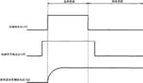
图2为说明图1所示的像素电路的操作序列的时序图。该时序图示出了用于对从信号线1F提供的视频信号的电位(视频信号线电位)进行采样、并使可为有机EL器件的发光器件1D进入发光状态的操作序列。当扫描线1E的电位(扫描线电位)升高时,采样晶体管1A导通,用视频信号线电位向保持电容器1C充电。驱动晶体管1B的栅极电位Vg开始升高,并且,驱动晶体管1B开始通过漏极电流。因此,发光器件D的阳极电位增加,导致发光器件D开始发光。当扫描线电位变低时,保持电容器1C保持视频信号线电位,从而保持驱动晶体管1B的栅极电位恒定。发光器件D的发光亮度一直保持恒定,直到下一帧为止。FIG. 2 is a timing diagram illustrating an operation sequence of the pixel circuit shown in FIG. 1 . This timing chart shows an operation sequence for sampling the potential of the video signal supplied from the signal line 1F (video signal line potential) and bringing the light emitting device 1D, which may be an organic EL device, into a light emitting state. When the potential of the scanning line 1E (scanning line potential) rises, the sampling transistor 1A is turned on, and the storage capacitor 1C is charged with the potential of the video signal line. The gate potential Vg of the drive transistor 1B starts to rise, and the drive transistor 1B starts to pass a drain current. Accordingly, the anode potential of the light emitting device D increases, causing the light emitting device D to start emitting light. When the scanning line potential becomes low, the holding capacitor 1C holds the video signal line potential, thereby keeping the gate potential of the driving transistor 1B constant. The light emitting brightness of the light emitting device D remains constant until the next frame.
由于像素电路的驱动晶体管1B的制造过程变化,显示设备的像素经受阈值电压和迁移率变化。由于那些特性变化,即使将相同的栅极电位施加到像素电路的驱动晶体管1B,像素还是具有它们自己的漏极电流(驱动电流)变化,其将作为发光亮度变化而出现。而且,可为有机EL器件的发光器件1D具有随时间变化的特性,从而导致发光器件1D的阳极电位的变化。发光器件1D的阳极电位的变化导致驱动晶体管1B的栅极到源极电位的变化,从而带来了漏极电流(驱动电流)的变化。多种原因造成的驱动电流的变化导致像素的发光亮度变化,这趋向于降低显示图像质量。The pixels of the display device are subject to threshold voltage and mobility variations due to variations in the manufacturing process of the drive transistor 1B of the pixel circuit. Due to those characteristic changes, even if the same gate potential is applied to the drive transistor 1B of the pixel circuit, the pixels have their own drain current (drive current) change, which will appear as a light emission luminance change. Also, the light emitting device 1D, which may be an organic EL device, has characteristics that vary with time, resulting in changes in the anode potential of the light emitting device 1D. A change in the anode potential of the light emitting device 1D causes a change in the gate-to-source potential of the drive transistor 1B, thereby bringing about a change in drain current (drive current). Variations in drive current due to various causes lead to variations in light emission luminance of pixels, which tends to degrade display image quality.
图3A以框图形式示出了根据本发明的实施例的显示设备的总体布置。如图3A所示,通常用标记100表示的显示设备包括像素阵列102和驱动器103、104、105。像素阵列102具有作为行的多个扫描线WSL101到WSL10m、作为列的多个信号线DTL101到DTL10n,像素矩阵(PXLC)101被设置在扫描线WSL101到WS10n与信号线DTL101到DTL10n的各个相交的位置,并且,多个电源线DSL101到DSL10m沿像素101的各行而被设置。驱动器包括:主扫描器(写入扫描器WSCN)104,用于向扫描线WSL101到WSL10m连续地提供控制信号,以在像素101的行上执行逐行扫描(line-sequential scan);电源扫描器(DSCN)105,用于与逐行扫描同步地向电源线DSL101到DSL10m提供可选择性地在第一电位和第二电位之间切换的电源电压;以及信号选择器(水平选择器(HSEL))103,用于与逐行扫描同步地向作为列的信号线DTL101到DTL10n提供作为视频信号的信号电位、以及参考电位。FIG. 3A shows the general arrangement of a display device according to an embodiment of the present invention in the form of a block diagram. As shown in FIG. 3A , a display device, generally indicated by
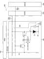
图3B为示出图3A所示的显示设备100的每个像素101的详细结构和互连的电路图。如图3B所示,像素101包括发光器件3D(典型地,为有机EL器件)、采样晶体管3A、驱动晶体管3B、以及保持电容器3C。采样晶体管3A具有与相应扫描线WSL101连接的栅极。采样晶体管3A的源极和漏极中的任一个与相应的信号线DTL101连接,而其源极和漏极中的另外一个与驱动晶体管3B的栅极g连接。驱动晶体管3B具有源极s和漏极d,源极s和漏极d中的任一个与发光器件3D连接,源极s和漏极d中的另一个与相应的电源线DSL101连接。在本实施例中,驱动晶体管3B的漏极d与电源线DSL101连接,并且,驱动晶体管3B的源极s与发光器件3D的阳极连接。发光器件3D的阴极与地线3H连接,所有像素101共同连接到地线3H。保持电容器3C连接在驱动晶体管3B的源极s和栅极g之间。FIG. 3B is a circuit diagram showing a detailed structure and interconnection of each
采样晶体管3A通过从扫描线WSL101提供的控制信号而呈现为导通,对从信号线DTL101提供的信号电位采样,并把采样的信号电位保持在保持电容器3C中。从第一电位上的电源线DSL101向驱动晶体管3B提供电流,并且,根据保持在保持电容器3C中的信号电位而向发光器件3D传递驱动电流。在采样晶体管3A呈现为导通之后,当信号选择器(HSEL)103正在向信号线DTL101提供参考电位时,电源扫描器(DSCN)105把电源线DSL101从第一电位切换到第二电位,从而在保持电容器3C中保持与驱动晶体管3B的阈值电压Vth基本相对应的电压。这样的阈值电压校正功能允许显示设备100消除逐像素而变化的驱动晶体管3B的阈值电压的影响。The
除了上述的阈值电压校正功能之外,如图3B所示的像素101还具有迁移率校正功能。具体地,在采样晶体管3A呈现为导通之后,信号选择器(HSEL)103在第一定时把信号线DTL101从参考电位切换到信号电位,并且,主扫描器(WSCN)104在第一定时后的第二定时停止向扫描线WSL101施加控制信号,因此,使采样晶体管3A呈现为非导通。适当地设置第一定时和第二定时之间的周期,以针对驱动晶体管3B的迁移率μ,而在信号电位被保持在保持电容器3C中时校正信号电位。驱动器103、104、105可以在视频选择器103所提供的视频信号和主扫描器104所提供的控制信号之间调整相关相位差,由此优化第一定时和第二定时之间的周期(迁移率校正周期)。信号选择器103还可以向从参考电位切换到信号电位的视频信号的上升沿施加梯度,由此允许第一定时和第二定时之间的迁移率校正周期自动跟随信号电位。In addition to the threshold voltage correction function described above, the
如图3B所示的像素101还具有自举功能。具体地,在保持电容器3C中保持信号电位时,主扫描器(WSCN)104停止向扫描线WSL101施加控制信号,由此使采样晶体管3A呈现为非导通,以断开驱动晶体管3B的栅极g与信号线DTL101的电连接。因此,栅极电位Vg与驱动晶体管3B的源极电位Vs的变化相关联,以保持栅极g和源极s之间的电压Vgs恒定。The
图4A为说明图3B所示的像素101的操作序列的时序图。图4A示出了沿公共时间轴的扫描线WSL101的电位变化、电源线DSL101的电位变化、和信号线DTL101的电位变化。除了上述电位变化以外,图4A还示出了驱动晶体管3B的栅极电位Vg和源极电位Vs的变化。FIG. 4A is a timing diagram illustrating an operation sequence of the
图4A所示的时序图被分成了像素101的不同操作周期(B)到(G)。具体地,在发光周期(B)中,发光器件3D为发光状态。其后,逐行扫描的新的扫描场开始,驱动晶体管3B的栅极电位Vg在第一周期(C)中被初始化。接着,在下一周期(D)中,驱动晶体管的源极电位Vs被初始化。驱动晶体管3B的栅极电位Vg和源极电位Vs被初始化后,像素101为阈值电压校正操作做好了充分的准备。在阈值电压校正周期(E)中,实际执行阈值电压校正操作,以在驱动晶体管3B的栅极g和源极s之间保持与阈值电压Vth基本上相对应的电压。实际上,与Vth相对应的电压被写入连接在驱动晶体管3B的栅极g和源极s之间的保持电容器3C中。接着,在采样周期/迁移率校正周期(F)中,除了阈值电压Vth以外,还将视频信号的信号电压Vin重新写入保持电容器3C中,并且,从保持电容器3C中保持的电压减去用来校正迁移率的电压ΔV。此后,在发光周期(G)中,发光器件3D根据信号电压Vin发出一定亮度级别的光。由于已通过与阈值电压Vth基本上相对应的电压、以及迁移率校正电压ΔV而调节了信号电压Vin,所以,发光器件3D的发光亮度不再不利地受阈值电压Vth和驱动晶体管3B的迁移率μ的影响。当驱动晶体管3B的栅极到源极的电压Vgs=Vin+Vth-ΔV保持恒定时,在发光周期(G)的初始阶段中进行自举操作,以增大驱动晶体管3B的栅极电位Vg和源极电位Vs。The timing diagram shown in FIG. 4A is divided into different operation periods (B) to (G) of the
下面结合图4B到4G而详细描述图3B所示的像素101的操作。图4B到4G示出了分别与图4A所示的时序图的周期(B)到(G)相对应的操作阶段。为了更简单地理解本发明,发光器件3D的电容部件在图4B到4G的每个中都被图解为电容元件31。如图4B所示,在发光周期(B)中,电源线DSL101处于高电位Vcc_H(第一电位),并且,驱动晶体管3B向发光器件3D提供驱动电流Ids。驱动电流Ids从处于高电位Vcc_H的电源线DSL101流过驱动晶体管3B和发光器件3D而进入公共地线3H。The operation of the
在周期(C)中,如图4C所示,扫描线WSL101变高,从而导通采样晶体管3A,以将驱动晶体管3B的栅极电位Vg初始化(重置)为视频线DTL101的参考电位Vo。In period (C), as shown in FIG. 4C , the scanning line WSL101 goes high to turn on the
在周期(D)中,如图4D所示,电源线DSL101从高电位Vcc_H(第一电位)切换到充分低于视频信号线DTL101的参考电位Vo的低电位Vcc_L(第二电位)。驱动晶体管3B的源极电位Vs被初始化(重置)为充分低于视频信号线DTL101的参考电位Vo的低电位Vcc_L。具体地,如此建立电源线DSL101的低电位Vcc_L(第二电位),使得驱动晶体管3B的栅极到源极电位Vgs(栅极电位Vg和源极电位Vs之间的差值)大于驱动晶体管3B的阈值电压Vth。In a period (D), as shown in FIG. 4D , the power supply line DSL101 switches from a high potential Vcc_H (first potential) to a low potential Vcc_L (second potential) sufficiently lower than the reference potential Vo of the video signal line DTL101 . The source potential Vs of the
阈值校正周期(E)中,如图4E所示,电源线DSL101从低电位Vcc_L切换到高电位Vcc_H,并且,驱动晶体管3B的源极电位Vs开始升高。当驱动晶体管3B的栅极到源极电位Vgs达到阈值电压Vth时,切断电流。这样,基本与驱动晶体管3B的阈值电压Vth相对应的电压被写入保持电容器3C。这个过程被称为阈值电压校正操作。为了使电流仅仅流入保持电容器3C、而不流入发光器件3D,设置公共地线3H的电位,以截止发光器件3D。In the threshold correction period (E), as shown in FIG. 4E , the power supply line DSL101 is switched from the low potential Vcc_L to the high potential Vcc_H, and the source potential Vs of the driving
在采样周期/迁移率校正周期(F),如图4F所示,视频信号线DTL101在第一定时从参考电位Vo变化到信号电位Vin,从而将驱动晶体管3B的栅极电位Vg设置为Vin。由于发光器件3D在这时初始为截止(位于高阻抗),所以,驱动晶体管3B的漏极电流Ids流入发光器件3D的寄生电容3I。发光器件3D的寄生电容3I现在开始被充电。因此,驱动晶体管3B的源极电位Vs开始升高,并且,驱动晶体管3B的栅极到源极电压Vgs在第二定时达到Vin+Vth-ΔV。这样,对信号电压Vin进行了采样,并调节了校正变量ΔV。Vin越高,Ids便越大,并且,ΔV的绝对值便越大。因此,可以执行根据发光亮度级别的迁移率校正。如果Vin恒定,那么,驱动晶体管3B的迁移率μ越大,ΔV的绝对值便越高。换句话说,由于负反馈变量ΔV随着迁移率μ的变大而变大,所以,有可能消除各个像素的迁移率μ的变化。In the sampling period/mobility correction period (F), as shown in FIG. 4F , the video signal line DTL101 changes from the reference potential Vo to the signal potential Vin at the first timing, thereby setting the gate potential Vg of the
最后,在发光周期(G)中,如图4G所示,扫描线WSL101转到低电位,从而关断采样晶体管3A。现在,驱动晶体管3B的栅极g与信号线DTL101分离。同时,漏极电流Ids开始流入发光器件3D。发光器件3D的阳极电位取决于驱动电流Ids而增高。发光器件3D的阳极电位的增加等价于驱动晶体管3B的源极电位Vs的升高。如同驱动晶体管3B的源极电位Vs那样,由于保持电容器3C的自举操作,驱动晶体管3B的栅极电位Vg也升高。栅极电位Vg的升高量与源极电位Vs的升高量相等。因此,在发光周期期间,驱动晶体管3B的栅极到源极电压Vgs保持在恒定电平Vin+Vth-ΔV。Finally, in the light emitting period (G), as shown in FIG. 4G , the scanning line WSL101 turns to low potential, thereby turning off the
图5为示出驱动晶体管3B的电流对电压特性的图。驱动晶体管3B的栅极到源极电流Ids在饱和区操作时,被表示为Ids=(1/2)·μ·(W/L)·Cox·(Vgs-Vth)2,其中μ代表迁移率,W代表栅极宽度,L代表栅极长度,而Cox代表单位面积上栅极氧化薄膜电容。如可从此晶体管特征方程中看出的,当阈值电压Vth变化时,即使Vgs恒定,漏极到源极电流Ids也变化。由于在像素发光时、栅极到源极电压Vgs被表示为Vin+Vth-ΔV,如果在上述晶体管特征方程中代入Vgs=Vin+Vth-ΔV,那么,漏极到源极电流被表示为Ids=(1/2)·μ·(W/L)·Cox·(Vin-ΔV)2,并且,不依赖于阈值电压Vth。结果,即使阈值电压Vth由于其制造过程而变化,漏极到源极电流Ids也不变,并且因此,有机EL器件的发光亮度不变。FIG. 5 is a graph showing the current versus voltage characteristics of the
如果不采取对策,那么如图5所示,在阈值电压为Vth时对应于栅极电压Vgs的驱动电流由Ids表示,而在阈值电压为Vth′时对应于相同的栅极电压Vgs的驱动电流由不同于Ids的Ids′表示。If no countermeasures are taken, then as shown in Figure 5, the drive current corresponding to the gate voltage Vgs when the threshold voltage is Vth is denoted by Ids, and the drive current corresponding to the same gate voltage Vgs when the threshold voltage is Vth' Denoted by Ids' different from Ids.
图6A也是示出不同驱动晶体管的电流对电压特性的图。图6A示出了两个具有不同迁移率μ、μ′的驱动晶体管的相应的特性曲线。如可由图6A的特性曲线看出的,如果驱动晶体管具有不同的迁移率μ、μ′,那么,即使栅极电压Vgs恒定,它们也具有不同的漏极到源极电流Ids、Ids′。FIG. 6A is also a graph showing the current versus voltage characteristics of different drive transistors. FIG. 6A shows the corresponding characteristic curves of two driver transistors with different mobilities μ, μ′. As can be seen from the characteristic curve of FIG. 6A, if the drive transistors have different mobilities μ, μ', they have different drain-to-source currents Ids, Ids' even if the gate voltage Vgs is constant.
图6B为说明如图3B所示的像素电路的用于对视频信号电位进行采样、并校正迁移率的操作的方式的电路图。为了更容易理解本发明,图6B还示出了发光器件3D的寄生电容3I。为了对视频信号电位Vin采样,导通采样晶体管3A。因此,驱动晶体管3B的栅极电位Vg被设置为视频信号电位Vin,并且,驱动晶体管3B的栅极到源极电压Vgs达到Vin+Vth。此时,导通驱动晶体管3B。由于截止了发光器件3D,所以,漏极到源极电流Ids流入发光器件电容3I。当漏极到源极电流Ids流入发光器件电容3I时,发光器件电容3I开始被充电,从而导致发光器件3D的阳极的电位(由此的驱动晶体管3B的源极电位Vs)开始升高。当驱动晶体管3B的源极电位Vs升高了ΔV时,驱动晶体管3B的栅极到源极电压Vgs减少了ΔV。这个过程被称为基于负反馈的迁移率校正操作。栅极到源极电压Vgs的减小量由ΔV=Ids·Cel/t确定,并用作迁移率校正的参数。其中,Cel代表发光器件电容3I的电容值,而t代表迁移率校正周期,即,第一定时和第二定时之间的周期。6B is a circuit diagram illustrating the manner of operation of the pixel circuit shown in FIG. 3B for sampling the video signal potential and correcting the mobility. For easier understanding of the present invention, FIG. 6B also shows the parasitic capacitance 3I of the
图6C示出了用于确定迁移率校正周期t的像素电路的操作时序图。在如图6C所示的例子中,向视频信号电位的上升沿施加梯度,由此允许迁移率校正周期自动跟随视频信号电位,从而优化迁移率校正周期t。如图6C所示,迁移率校正周期t由扫描线WSL101和视频信号线DTL101之间的相位差来确定,并且,还由视频信号线DTL101的电位确定。迁移率校正参数ΔV被表示为ΔV=Ids·cel/t。如从此方程可以看出的,随着驱动晶体管3B的漏极到源极电流Ids变大,迁移率校正参数ΔV变大。相反,当驱动晶体管3B的漏极到源极电流Ids变小时,迁移率校正参数ΔV变小。因此,迁移率校正参数ΔV依赖于漏极到源极电流Ids而被确定。迁移率校正周期t不一定为常量,但是,在某些情况下,优选应根据Ids而调整迁移率校正周期t。例如,如果Ids变大,那么迁移率校正周期t应变短,而如果Ids变小,那么迁移率校正周期t应变长。在如图6C所示的例子中,至少向视频信号电位的上升沿施加梯度,以自动地调节迁移率校正周期t,使得在视频信号线DTL101的电位变高(Ids变大)时,迁移率校正周期t变短,而视频信号线DTL101的电位变低(Ids变小)时,迁移率校正周期t变长。FIG. 6C shows an operation timing chart of the pixel circuit for determining the mobility correction period t. In the example shown in FIG. 6C, a gradient is applied to the rising edge of the video signal potential, thereby allowing the mobility correction period to automatically follow the video signal potential, thereby optimizing the mobility correction period t. As shown in FIG. 6C, the mobility correction period t is determined by the phase difference between the scanning line WSL101 and the video signal line DTL101, and is also determined by the potential of the video signal line DTL101. The mobility correction parameter ΔV is expressed as ΔV=Ids·cel/t. As can be seen from this equation, as the drain-to-source current Ids of the
图6D为说明校正迁移率时的驱动晶体管3B的操作点的图。当对由于制造过程引起的不同的迁移率μ、μ′执行上述迁移率校正时,确定最佳的校正参数ΔV、ΔV′,以确定驱动晶体管3B的漏极到源极电流Ids、Ids′。在无迁移率校正的情况下,如果关于栅极到源极电压Vgs而给出不同的迁移率μ、μ’,那么,产生对应地不同的漏极到源极电流Ids0、Ids0′。为了解决上述问题,将适当的校正参数ΔV、ΔV′分别应用于不同的迁移率μ、μ′,以在相同级别上确定漏极到源极电流Ids,Ids′。通过回顾图6D所示的图,清楚地示出:施加负反馈,以使在迁移率μ变大时,校正变量ΔV也变大,并还使在迁移率μ′变小时,校正变量ΔV′也变小。FIG. 6D is a graph illustrating the operating point of the driving
图7A为示出作为有机EL器件的形式的发光器件3D的电流对电压特性的图。当电流Iel开始流入发光器件3D时,唯一地确定阳极到阴极电压Vel。当扫描线WSL101转到低电位时,关断采样晶体管3A,如图4G所示,发光器件3D的阳极电位升高了由驱动晶体管3B的漏极到源极电流Ids确定的阳极到阴极电压Vel。FIG. 7A is a graph showing current versus voltage characteristics of a
图7B为示出在发光器件3D的阳极电位升高时的驱动晶体管3B的栅极电位Vg和源极电位Vs的电位变化的图。当发光器件3D的阳极电位增加了Vel时,驱动晶体管3B的源极电位Vs也增加Vel,并且,由于保持电容器3C的自举操作,驱动晶体管3B的栅极电位Vg也增加Vel。因此,在自举操作之前保持的驱动晶体管3的栅极到源极电压Vgs=Vin+Vth-ΔV在自举操作之后同样保持。即使由于发光器件3D的老化而导致发光器件3D的阳极电位变化,驱动晶体管3B的栅极到源极电位在所有时间都保持为恒定电平Vin+Vth-ΔV。7B is a graph showing potential changes of the gate potential Vg and the source potential Vs of the
图7C为如图3B所示的像素电路的电路图,其中图解了寄生电容7A、7B。寄生电容7A、7B被以寄生方式添加到驱动晶体管3B的栅极g。上述的自举操作能力被称为Cs/(Cs+Cw+Cp),其中Cs代表保持电容器3C的电容值,而Cw,Cp为寄生电容7A、7B的相应的电容值。随着Cs/(Cs+Cw+Cp)越来越接近1,自举操作能力越高,也就是说,针对发光器件3D老化的校正能力越高。根据本发明的实施例,连接在驱动晶体管3B栅极g上的装置的数目被保持在最小。因此,电容值Cp可被忽略。因此,自举操作能力可被表示为Cs/(Cs+Cw),其极接近1,从而表示针对发光器件3D的老化的校正性能很高。Fig. 7C is a circuit diagram of the pixel circuit shown in Fig. 3B, in which
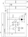
图8为根据本发明的另一实施例的显示设备的像素电路的电路图。为了更容易理解本发明,图8中与图3B相应的部分用相应的附图标记表示。图8所示的像素电路与图3所示的像素电路的不同之处在于,尽管图3所示的像素电路采用N型晶体管,但图8所示像素电路采用P型晶体管。图8所示的像素电路能够以与图3所示的像素电路完全一样的实施方式执行阈值电压校正操作、迁移率校正操作和自举操作。FIG. 8 is a circuit diagram of a pixel circuit of a display device according to another embodiment of the present invention. For easier understanding of the present invention, parts in FIG. 8 corresponding to those in FIG. 3B are denoted by corresponding reference numerals. The difference between the pixel circuit shown in FIG. 8 and the pixel circuit shown in FIG. 3 is that although the pixel circuit shown in FIG. 3 uses N-type transistors, the pixel circuit shown in FIG. 8 uses P-type transistors. The pixel circuit shown in FIG. 8 is capable of performing a threshold voltage correction operation, a mobility correction operation, and a bootstrap operation in exactly the same manner as the pixel circuit shown in FIG. 3 .
如上所述的根据本发明的实施例的显示设备可以用作用于如图9A到图9G所示的各个电子单元的显示设备,包括数码相机、笔记本式个人计算机、蜂窝式电话单元、摄像机等,以便将在电子单元中生成的视频信号显示为静态图像、或者视频图像。The display device according to the embodiment of the present invention as described above can be used as a display device for various electronic units as shown in FIGS. 9A to 9G , including digital cameras, notebook personal computers, cellular phone units, video cameras, etc., In order to display the video signal generated in the electronic unit as a still image or as a video image.
根据本发明的实施例的显示设备可以是如图10所示的模块配置,例如,具有应用于透明面单元(transparent facing unit)的像素矩阵的显示模块。显示模块可包括滤色器、保护膜、和光阻膜等,其被置于透明面单元上。显示模块还可以具有FPCs(多个柔性印刷电路),用于输入信号到像素矩阵、以及从像素矩阵输出信号。A display device according to an embodiment of the present invention may be a module configuration as shown in FIG. 10, for example, a display module having a pixel matrix applied to a transparent facing unit. The display module may include a color filter, a protective film, a photoresist film, etc., which are placed on the transparent face unit. The display module may also have FPCs (flexible printed circuits) for inputting signals to and outputting signals from the pixel matrix.
下面描述如图9A到图9G所示的电子单元。The electronic unit shown in FIGS. 9A to 9G is described below.
图9A示出了具有由前面板2等制成的视频显示屏1的电视机。根据本发明的实施例的显示设备被并入视频显示屏1中。FIG. 9A shows a television set having a video display screen 1 made of a
图9B和图9C示出了数码相机,其包括图像捕捉镜头1、闪烁发光单元2、显示单元3等。根据本发明的实施例的显示设备被并入显示单元3中。9B and 9C illustrate a digital camera including an image capturing lens 1, a blinking
图9D示出了摄像机,其包括主体1、显示面板2等。根据本发明的实施例的显示设备被并入显示面板2中。FIG. 9D shows a camera, which includes a main body 1, a
图9E和图9F示出了蜂窝式电话单元,其包括显示面板1、辅助显示面板2等。根据本发明一个实施例的显示设备被并入显示面板1和辅助显示面板2。9E and 9F show a cellular phone unit including a display panel 1, an
图9G示出了笔记本式个人计算机,其包括具有用于输入字符的键盘2等的主体1、以及用于显示图像的显示面板3。根据本发明的实施例的显示设备被并入显示面板3中。FIG. 9G shows a notebook type personal computer including a main body 1 having a
尽管详细描述和示出了根据本发明特定优选实施例,但应该理解,根据其所作的各种变化和修改都没有脱离开所附权利要求的范围。Although certain preferred embodiments according to the present invention have been described and shown in detail, it should be understood that various changes and modifications can be made thereon without departing from the scope of the appended claims.
Claims (5)
Translated fromChineseApplications Claiming Priority (2)
| Application Number | Priority Date | Filing Date | Title |
|---|---|---|---|
| JP141836/06 | 2006-05-22 | ||
| JP2006141836AJP4240059B2 (en) | 2006-05-22 | 2006-05-22 | Display device and driving method thereof |
Related Parent Applications (1)
| Application Number | Title | Priority Date | Filing Date |
|---|---|---|---|
| CN200710142109ADivisionCN100587775C (en) | 2006-05-22 | 2007-05-22 | Display device and method of driving the same |
Publications (2)
| Publication Number | Publication Date |
|---|---|
| CN101577089A CN101577089A (en) | 2009-11-11 |
| CN101577089Btrue CN101577089B (en) | 2013-03-27 |
Family
ID=38291197
Family Applications (2)
| Application Number | Title | Priority Date | Filing Date |
|---|---|---|---|
| CN2009101411170AActiveCN101577089B (en) | 2006-05-22 | 2007-05-22 | Display apparatus and method of driving same |
| CN200710142109AActiveCN100587775C (en) | 2006-05-22 | 2007-05-22 | Display device and method of driving the same |
Family Applications After (1)
| Application Number | Title | Priority Date | Filing Date |
|---|---|---|---|
| CN200710142109AActiveCN100587775C (en) | 2006-05-22 | 2007-05-22 | Display device and method of driving the same |
Country Status (6)
| Country | Link |
|---|---|
| US (2) | US7768485B2 (en) |
| EP (2) | EP2341495B1 (en) |
| JP (1) | JP4240059B2 (en) |
| KR (1) | KR101424693B1 (en) |
| CN (2) | CN101577089B (en) |
| TW (1) | TW200813955A (en) |
Families Citing this family (191)
| Publication number | Priority date | Publication date | Assignee | Title |
|---|---|---|---|---|
| JP4240059B2 (en) | 2006-05-22 | 2009-03-18 | ソニー株式会社 | Display device and driving method thereof |
| JP4240068B2 (en) | 2006-06-30 | 2009-03-18 | ソニー株式会社 | Display device and driving method thereof |
| JP5114889B2 (en)* | 2006-07-27 | 2013-01-09 | ソニー株式会社 | Display element, display element drive method, display device, and display device drive method |
| JP4984863B2 (en)* | 2006-12-08 | 2012-07-25 | ソニー株式会社 | Display device and driving method thereof |
| JP4337897B2 (en)* | 2007-03-22 | 2009-09-30 | ソニー株式会社 | Display device, driving method thereof, and electronic apparatus |
| JP4470960B2 (en)* | 2007-05-21 | 2010-06-02 | ソニー株式会社 | Display device, driving method thereof, and electronic apparatus |
| JP2008310128A (en)* | 2007-06-15 | 2008-12-25 | Sony Corp | Display device, display device driving method, and electronic apparatus |
| KR101526475B1 (en) | 2007-06-29 | 2015-06-05 | 가부시키가이샤 한도오따이 에네루기 켄큐쇼 | Display device and driving method thereof |
| JP2009031620A (en)* | 2007-07-30 | 2009-02-12 | Sony Corp | Display device and driving method of display device |
| JP2009063719A (en)* | 2007-09-05 | 2009-03-26 | Sony Corp | Method of driving organic electroluminescence emission part |
| JP4428436B2 (en) | 2007-10-23 | 2010-03-10 | ソニー株式会社 | Display device and electronic device |
| JP2009133913A (en)* | 2007-11-28 | 2009-06-18 | Sony Corp | Display device |
| JP5256710B2 (en)* | 2007-11-28 | 2013-08-07 | ソニー株式会社 | EL display panel |
| JP2009139671A (en)* | 2007-12-07 | 2009-06-25 | Sony Corp | Display device, method of driving display device and electronic device |
| JP2009145531A (en)* | 2007-12-13 | 2009-07-02 | Sony Corp | Display, driving method for display, and electronic equipment |
| JP5176522B2 (en)* | 2007-12-13 | 2013-04-03 | ソニー株式会社 | Self-luminous display device and driving method thereof |
| JP5194781B2 (en) | 2007-12-26 | 2013-05-08 | ソニー株式会社 | Display device, driving method thereof, and electronic apparatus |
| JP4715849B2 (en) | 2008-01-15 | 2011-07-06 | ソニー株式会社 | Display device, driving method thereof, and electronic apparatus |
| JP4591511B2 (en)* | 2008-01-15 | 2010-12-01 | ソニー株式会社 | Display device and electronic device |
| JP4715850B2 (en)* | 2008-01-15 | 2011-07-06 | ソニー株式会社 | Display device, driving method thereof, and electronic apparatus |
| JP2009169071A (en) | 2008-01-16 | 2009-07-30 | Sony Corp | Display device |
| JP2009175198A (en) | 2008-01-21 | 2009-08-06 | Sony Corp | El display panel and electronic apparatus |
| JP4816653B2 (en)* | 2008-02-04 | 2011-11-16 | ソニー株式会社 | Display device, driving method thereof, and electronic apparatus |
| JP4438869B2 (en)* | 2008-02-04 | 2010-03-24 | ソニー株式会社 | Display device, driving method thereof, and electronic apparatus |
| JP5186950B2 (en)* | 2008-02-28 | 2013-04-24 | ソニー株式会社 | EL display panel, electronic device, and driving method of EL display panel |
| JP2009204978A (en)* | 2008-02-28 | 2009-09-10 | Sony Corp | El display panel module, el display panel, and electronic device |
| JP2009237558A (en)* | 2008-03-05 | 2009-10-15 | Semiconductor Energy Lab Co Ltd | Driving method for semiconductor device |
| KR100911978B1 (en) | 2008-03-10 | 2009-08-13 | 삼성모바일디스플레이주식회사 | Pixel and organic light emitting display device using same |
| JP2009237041A (en)* | 2008-03-26 | 2009-10-15 | Sony Corp | Image displaying apparatus and image display method |
| JP5245879B2 (en) | 2008-03-26 | 2013-07-24 | ソニー株式会社 | Image display device and method of repairing short circuit accident |
| JP4780134B2 (en) | 2008-04-09 | 2011-09-28 | ソニー株式会社 | Image display device and driving method of image display device |
| JP4826598B2 (en)* | 2008-04-09 | 2011-11-30 | ソニー株式会社 | Image display device and driving method of image display device |
| JP2009258301A (en)* | 2008-04-15 | 2009-11-05 | Eastman Kodak Co | Display device |
| JP2009258275A (en)* | 2008-04-15 | 2009-11-05 | Sony Corp | Display device and output buffer circuit |
| JP4737221B2 (en)* | 2008-04-16 | 2011-07-27 | ソニー株式会社 | Display device |
| JP4640443B2 (en) | 2008-05-08 | 2011-03-02 | ソニー株式会社 | Display device, display device driving method, and electronic apparatus |
| JP2009294635A (en)* | 2008-05-08 | 2009-12-17 | Sony Corp | Display device, method for driving display device thereof, and electronic equipment |
| JP4640442B2 (en) | 2008-05-08 | 2011-03-02 | ソニー株式会社 | Display device, display device driving method, and electronic apparatus |
| JP4582195B2 (en) | 2008-05-29 | 2010-11-17 | ソニー株式会社 | Display device |
| JP4640449B2 (en)* | 2008-06-02 | 2011-03-02 | ソニー株式会社 | Display device, driving method thereof, and electronic apparatus |
| JP2009288734A (en) | 2008-06-02 | 2009-12-10 | Sony Corp | Image display device |
| KR100922065B1 (en) | 2008-06-11 | 2009-10-19 | 삼성모바일디스플레이주식회사 | Pixel and organic light emitting display device using same |
| JP5235516B2 (en) | 2008-06-13 | 2013-07-10 | 富士フイルム株式会社 | Display device and driving method |
| JP2009300853A (en)* | 2008-06-16 | 2009-12-24 | Sony Corp | Display device and method of driving the same, and electronic device |
| JP4614106B2 (en) | 2008-06-18 | 2011-01-19 | ソニー株式会社 | Self-luminous display device and electronic device |
| JP2010002498A (en)* | 2008-06-18 | 2010-01-07 | Sony Corp | Panel and drive control method |
| JP2010002736A (en)* | 2008-06-20 | 2010-01-07 | Toshiba Mobile Display Co Ltd | El display |
| JP4784780B2 (en)* | 2008-06-30 | 2011-10-05 | ソニー株式会社 | Display device, driving method thereof, and electronic apparatus |
| JP2010020034A (en) | 2008-07-10 | 2010-01-28 | Sony Corp | Image display device |
| JP4544355B2 (en)* | 2008-08-04 | 2010-09-15 | ソニー株式会社 | Pixel circuit, driving method thereof, display device, and driving method thereof |
| JP5027755B2 (en)* | 2008-08-04 | 2012-09-19 | ソニー株式会社 | Display device and driving method thereof |
| JP2010039118A (en) | 2008-08-04 | 2010-02-18 | Sony Corp | Display and electronic equipment |
| JP2010039176A (en)* | 2008-08-05 | 2010-02-18 | Sony Corp | Image display, and method for driving image device |
| JP2010039397A (en) | 2008-08-08 | 2010-02-18 | Sony Corp | Display and electronic device |
| JP2010039436A (en)* | 2008-08-08 | 2010-02-18 | Sony Corp | Display panel module and electronic apparatus |
| JP5107824B2 (en)* | 2008-08-18 | 2012-12-26 | 富士フイルム株式会社 | Display device and drive control method thereof |
| US8310416B2 (en) | 2008-08-18 | 2012-11-13 | Seiko Epson Corporation | Method of driving pixel circuit, light-emitting apparatus, and electronic apparatus |
| JP2010049041A (en) | 2008-08-22 | 2010-03-04 | Sony Corp | Image display device and driving method of the image display device |
| JP5384051B2 (en)* | 2008-08-27 | 2014-01-08 | 株式会社ジャパンディスプレイ | Image display device |
| JP2010060601A (en) | 2008-09-01 | 2010-03-18 | Sony Corp | Image display apparatus and method for driving the same |
| US8599222B2 (en) | 2008-09-04 | 2013-12-03 | Seiko Epson Corporation | Method of driving pixel circuit, light emitting device, and electronic apparatus |
| JP2010060873A (en) | 2008-09-04 | 2010-03-18 | Sony Corp | Image display device |
| JP5412770B2 (en) | 2008-09-04 | 2014-02-12 | セイコーエプソン株式会社 | Pixel circuit driving method, light emitting device, and electronic apparatus |
| JP5458540B2 (en)* | 2008-09-29 | 2014-04-02 | セイコーエプソン株式会社 | Pixel circuit driving method, light emitting device, and electronic apparatus |
| JP5439782B2 (en) | 2008-09-29 | 2014-03-12 | セイコーエプソン株式会社 | Pixel circuit driving method, light emitting device, and electronic apparatus |
| JP5401895B2 (en)* | 2008-09-29 | 2014-01-29 | セイコーエプソン株式会社 | Pixel circuit driving method, light emitting device, and electronic apparatus |
| KR101498094B1 (en) | 2008-09-29 | 2015-03-05 | 삼성디스플레이 주식회사 | Display device and driving method thereof |
| JP5088294B2 (en) | 2008-10-29 | 2012-12-05 | ソニー株式会社 | Image display device and driving method of image display device |
| JP2010107630A (en) | 2008-10-29 | 2010-05-13 | Sony Corp | Image display device and method for driving image display device |
| JP2010113188A (en) | 2008-11-07 | 2010-05-20 | Sony Corp | Organic electroluminescence emitting unit driving method |
| JP2010117475A (en)* | 2008-11-12 | 2010-05-27 | Sony Corp | Display apparatus, electronic device, and method of driving the display apparatus |
| KR100986915B1 (en) | 2008-11-26 | 2010-10-08 | 삼성모바일디스플레이주식회사 | Organic light emitting display device and driving method thereof |
| KR100986896B1 (en) | 2008-12-05 | 2010-10-08 | 삼성모바일디스플레이주식회사 | Organic light emitting display device and driving method thereof |
| JP4957713B2 (en) | 2008-12-08 | 2012-06-20 | ソニー株式会社 | Driving method of organic electroluminescence display device |
| JP5168116B2 (en)* | 2008-12-11 | 2013-03-21 | ソニー株式会社 | Display device, display device driving method, and electronic apparatus |
| JP5239812B2 (en) | 2008-12-11 | 2013-07-17 | ソニー株式会社 | Display device, display device driving method, and electronic apparatus |
| JP5277926B2 (en)* | 2008-12-15 | 2013-08-28 | ソニー株式会社 | Display device, driving method thereof, and electronic apparatus |
| JP2010145578A (en)* | 2008-12-17 | 2010-07-01 | Sony Corp | Display device, method of driving display device, and electronic apparatus |
| JP2010145581A (en) | 2008-12-17 | 2010-07-01 | Sony Corp | Display device, method of driving display device, and electronic apparatus |
| KR101056241B1 (en) | 2008-12-19 | 2011-08-11 | 삼성모바일디스플레이주식회사 | Organic light emitting display |
| JP4930501B2 (en) | 2008-12-22 | 2012-05-16 | ソニー株式会社 | Display device and electronic device |
| JP5449785B2 (en)* | 2009-01-06 | 2014-03-19 | 株式会社ジャパンディスプレイ | Active matrix organic light emitting display |
| JP4844634B2 (en)* | 2009-01-06 | 2011-12-28 | ソニー株式会社 | Driving method of organic electroluminescence light emitting unit |
| JP2010170018A (en) | 2009-01-26 | 2010-08-05 | Seiko Epson Corp | Light-emitting device, driving method thereof, and electronic apparatus |
| WO2010087420A1 (en) | 2009-01-30 | 2010-08-05 | Fujifilm Corporation | Driving of oled display device with interleaving of control phases |
| TWI453910B (en) | 2009-02-04 | 2014-09-21 | Sony Corp | Image display device and repair method of short circuit accident |
| JP2010181788A (en)* | 2009-02-09 | 2010-08-19 | Sony Corp | Display device and its driving method |
| US9047815B2 (en) | 2009-02-27 | 2015-06-02 | Semiconductor Energy Laboratory Co., Ltd. | Method for driving semiconductor device |
| JP5736114B2 (en) | 2009-02-27 | 2015-06-17 | 株式会社半導体エネルギー研究所 | Semiconductor device driving method and electronic device driving method |
| KR101056228B1 (en) | 2009-03-02 | 2011-08-11 | 삼성모바일디스플레이주식회사 | Organic light emitting display |
| KR101056240B1 (en) | 2009-03-02 | 2011-08-11 | 삼성모바일디스플레이주식회사 | Organic light emitting display |
| JP4844641B2 (en) | 2009-03-12 | 2011-12-28 | ソニー株式会社 | Display device and driving method thereof |
| CN101847648B (en)* | 2009-03-23 | 2012-11-21 | 北京京东方光电科技有限公司 | Active matrix organic light-emitting diode pixel structure and manufacturing method thereof |
| KR101056302B1 (en) | 2009-03-26 | 2011-08-11 | 삼성모바일디스플레이주식회사 | Organic light emitting display |
| JP5262930B2 (en) | 2009-04-01 | 2013-08-14 | ソニー株式会社 | Display element driving method and display device driving method |
| JP5278119B2 (en)* | 2009-04-02 | 2013-09-04 | ソニー株式会社 | Driving method of display device |
| JP5458671B2 (en) | 2009-05-29 | 2014-04-02 | セイコーエプソン株式会社 | LIGHT EMITTING DEVICE, LIGHT EMITTING DEVICE DRIVE METHOD, AND ELECTRONIC DEVICE |
| JP5293417B2 (en) | 2009-06-03 | 2013-09-18 | ソニー株式会社 | Driving method of display device |
| JP5326850B2 (en) | 2009-06-18 | 2013-10-30 | セイコーエプソン株式会社 | LIGHT EMITTING DEVICE, LIGHT EMITTING DEVICE DRIVE METHOD, AND ELECTRONIC DEVICE |
| JP2011002651A (en)* | 2009-06-18 | 2011-01-06 | Canon Inc | Image display device and control method of image display device |
| JP2011008161A (en)* | 2009-06-29 | 2011-01-13 | Seiko Epson Corp | Light emitting device and electronic equipment, method of driving pixel circuit |
| KR101056281B1 (en) | 2009-08-03 | 2011-08-11 | 삼성모바일디스플레이주식회사 | Organic electroluminescent display and driving method thereof |
| KR101056308B1 (en) | 2009-10-19 | 2011-08-11 | 삼성모바일디스플레이주식회사 | Organic light emitting display device and driving method thereof |
| KR102162746B1 (en)* | 2009-10-21 | 2020-10-07 | 가부시키가이샤 한도오따이 에네루기 켄큐쇼 | Analog circuit and semiconductor device |
| JP5493733B2 (en)* | 2009-11-09 | 2014-05-14 | ソニー株式会社 | Display device and electronic device |
| JP2011112724A (en)* | 2009-11-24 | 2011-06-09 | Sony Corp | Display device, method of driving the same and electronic equipment |
| KR101056318B1 (en) | 2009-12-31 | 2011-08-11 | 삼성모바일디스플레이주식회사 | Pixel and organic light emitting display device using same |
| JP5577719B2 (en)* | 2010-01-28 | 2014-08-27 | ソニー株式会社 | Display device, driving method thereof, and electronic apparatus |
| JP5007844B2 (en)* | 2010-01-29 | 2012-08-22 | ソニー株式会社 | EL display panel and electronic device |
| JP2011170244A (en) | 2010-02-22 | 2011-09-01 | Sony Corp | Display device, method for driving display device, and method for driving display element |
| AU2011236333B2 (en) | 2010-04-02 | 2014-02-27 | Sharp Kabushiki Kaisha | Display device and drive method therefor |
| KR101452655B1 (en) | 2010-07-12 | 2014-10-22 | 샤프 가부시키가이샤 | Display device and method for driving same |
| KR101348537B1 (en) | 2010-09-29 | 2014-01-07 | 파나소닉 주식회사 | El display panel, el display device and method for manufacturing el display panel |
| WO2012042565A1 (en) | 2010-09-29 | 2012-04-05 | パナソニック株式会社 | El display panel, el display device, and method for producing el display panel |
| WO2012042566A1 (en) | 2010-09-29 | 2012-04-05 | パナソニック株式会社 | Thin-film semiconductor device for display device, method for producing thin-film semiconductor device for display device, el display panel and el display device |
| JP5721736B2 (en) | 2010-10-21 | 2015-05-20 | シャープ株式会社 | Display device and driving method thereof |
| JP5696463B2 (en) | 2010-12-15 | 2015-04-08 | ソニー株式会社 | Display device and driving method of display device |
| JP5625864B2 (en) | 2010-12-15 | 2014-11-19 | ソニー株式会社 | Display device and driving method of display device |
| JP5652188B2 (en) | 2010-12-15 | 2015-01-14 | ソニー株式会社 | Display device |
| JP5633357B2 (en) | 2010-12-15 | 2014-12-03 | ソニー株式会社 | Display device and driving method of display device |
| KR101839533B1 (en) | 2010-12-28 | 2018-03-19 | 삼성디스플레이 주식회사 | Organic light emitting display device, driving method for the same, and method for manufacturing the same |
| JP5644511B2 (en) | 2011-01-06 | 2014-12-24 | ソニー株式会社 | Organic EL display device and electronic device |
| JP5682385B2 (en) | 2011-03-10 | 2015-03-11 | セイコーエプソン株式会社 | Electro-optical device and electronic apparatus |
| JP5803232B2 (en) | 2011-04-18 | 2015-11-04 | セイコーエプソン株式会社 | Organic EL device and electronic device |
| JP6018409B2 (en) | 2011-05-13 | 2016-11-02 | 株式会社半導体エネルギー研究所 | Light emitting device |
| JP2012237919A (en) | 2011-05-13 | 2012-12-06 | Sony Corp | Pixel circuit, display device, electronic apparatus and drive method of pixel circuit |
| JP6109489B2 (en) | 2011-05-13 | 2017-04-05 | 株式会社半導体エネルギー研究所 | EL display device |
| JP6110075B2 (en) | 2011-05-13 | 2017-04-05 | 株式会社半導体エネルギー研究所 | Display device |
| CN102800274B (en)* | 2011-05-26 | 2015-03-25 | 群康科技(深圳)有限公司 | Display device and control method thereof |
| US9053665B2 (en)* | 2011-05-26 | 2015-06-09 | Innocom Technology (Shenzhen) Co., Ltd. | Display device and control method thereof without flicker issues |
| JP5686043B2 (en) | 2011-06-02 | 2015-03-18 | セイコーエプソン株式会社 | Electro-optical device and electronic apparatus |
| JP5842263B2 (en) | 2011-06-08 | 2016-01-13 | 株式会社Joled | Display element, display device, and electronic device |
| JP5842264B2 (en) | 2011-06-08 | 2016-01-13 | 株式会社Joled | Display device and electronic device |
| JP5891492B2 (en) | 2011-06-22 | 2016-03-23 | 株式会社Joled | Display element, display device, and electronic device |
| JP5795893B2 (en)* | 2011-07-07 | 2015-10-14 | 株式会社Joled | Display device, display element, and electronic device |
| JP5870546B2 (en) | 2011-08-23 | 2016-03-01 | ソニー株式会社 | Display device and electronic device |
| JP2013044891A (en) | 2011-08-23 | 2013-03-04 | Sony Corp | Display device and electronic apparatus |
| JP5780649B2 (en) | 2011-11-11 | 2015-09-16 | 株式会社Joled | Buffer circuit, scanning circuit, display device, and electronic device |
| JP5780650B2 (en) | 2011-11-11 | 2015-09-16 | 株式会社Joled | Level shifter circuit, scanning circuit, display device, and electronic device |
| US9460660B2 (en) | 2011-12-21 | 2016-10-04 | Sharp Kabushiki Kaisha | Pixel circuit and display device |
| JP6108856B2 (en) | 2012-03-09 | 2017-04-05 | キヤノン株式会社 | Display device, electronic device using the same, and display device driving method |
| CN104520918B (en) | 2012-08-02 | 2016-08-31 | 夏普株式会社 | Display device and driving method thereof |
| JP6031652B2 (en)* | 2012-08-31 | 2016-11-24 | 株式会社Joled | Display device and electronic device |
| JP2014048485A (en) | 2012-08-31 | 2014-03-17 | Sony Corp | Display device and electronic apparatus |
| TWI559064B (en) | 2012-10-19 | 2016-11-21 | Japan Display Inc | Display device |
| TWI511113B (en) | 2012-10-19 | 2015-12-01 | Japan Display Inc | Display device |
| JP6082908B2 (en) | 2012-11-13 | 2017-02-22 | 株式会社Joled | Display device and driving method of display device |
| KR20140064170A (en)* | 2012-11-19 | 2014-05-28 | 삼성디스플레이 주식회사 | Display device, power control device and driving method thereof |
| US9953563B2 (en) | 2013-04-23 | 2018-04-24 | Sharp Kabushiki Kaisha | Display device and drive current detection method for same |
| US10453398B2 (en) | 2013-06-20 | 2019-10-22 | Sharp Kabushiki Kaisha | Display apparatus and driving method thereof |
| JP2015034861A (en) | 2013-08-08 | 2015-02-19 | ソニー株式会社 | Display device, driving method of display device, and electronic apparatus |
| JP2015043008A (en)* | 2013-08-26 | 2015-03-05 | 株式会社ジャパンディスプレイ | Organic EL display device |
| JP6153830B2 (en) | 2013-09-13 | 2017-06-28 | 株式会社ジャパンディスプレイ | Display device and driving method thereof |
| JP6495602B2 (en) | 2013-09-13 | 2019-04-03 | 株式会社半導体エネルギー研究所 | Light emitting device |
| JP2015060020A (en)* | 2013-09-18 | 2015-03-30 | ソニー株式会社 | Display device and electronic device |
| KR102053444B1 (en)* | 2013-11-06 | 2019-12-06 | 엘지디스플레이 주식회사 | Organic Light Emitting Display And Mobility Compensation Method Thereof |
| JP2015102793A (en) | 2013-11-27 | 2015-06-04 | 株式会社ジャパンディスプレイ | Display device and method for driving display device |
| JP2015125366A (en)* | 2013-12-27 | 2015-07-06 | 株式会社ジャパンディスプレイ | Display device |
| JP6300534B2 (en) | 2014-01-17 | 2018-03-28 | 株式会社ジャパンディスプレイ | Display device |
| JP6333951B2 (en) | 2014-03-13 | 2018-05-30 | 株式会社Joled | EL display device |
| JP2015225150A (en) | 2014-05-27 | 2015-12-14 | ソニー株式会社 | Display device and electronic apparatus |
| KR102190161B1 (en)* | 2014-06-23 | 2020-12-14 | 삼성디스플레이 주식회사 | Pixel, display panel and organic light emitting display including the same |
| KR101640192B1 (en)* | 2014-08-05 | 2016-07-18 | 삼성디스플레이 주식회사 | Display apparatus |
| US10170055B2 (en) | 2014-09-26 | 2019-01-01 | Semiconductor Energy Laboratory Co., Ltd. | Display device and driving method thereof |
| KR102244075B1 (en)* | 2014-10-29 | 2021-04-26 | 삼성디스플레이 주식회사 | Apparatus for scan driving and display apparatus using thereof |
| US10002564B2 (en) | 2014-10-31 | 2018-06-19 | Semiconductor Energy Laboratory Co., Ltd. | Display device, display module, and electronic device |
| JP6618779B2 (en) | 2014-11-28 | 2019-12-11 | 株式会社半導体エネルギー研究所 | Semiconductor device |
| TWI682632B (en) | 2014-12-26 | 2020-01-11 | 日商半導體能源研究所股份有限公司 | Semiconductor device |
| JP2016177280A (en)* | 2015-03-18 | 2016-10-06 | 株式会社半導体エネルギー研究所 | Display device, electronic device, and driving method of display device |
| JP6518471B2 (en) | 2015-03-19 | 2019-05-22 | 株式会社ジャパンディスプレイ | Light emitting element display |
| CN104680982B (en)* | 2015-03-27 | 2017-03-08 | 深圳市华星光电技术有限公司 | AMOLED pixel-driving circuit and image element driving method |
| JP2016206659A (en) | 2015-04-16 | 2016-12-08 | 株式会社半導体エネルギー研究所 | Display device, electronic device, and method for driving display device |
| US10424246B2 (en) | 2015-07-21 | 2019-09-24 | Shenzhen Royole Technologies Co., Ltd. | Pixel circuit and method for driving pixel circuit |
| US9704893B2 (en) | 2015-08-07 | 2017-07-11 | Semiconductor Energy Laboratory Co., Ltd. | Semiconductor device and electronic device |
| JP6164269B2 (en)* | 2015-09-30 | 2017-07-19 | セイコーエプソン株式会社 | Electro-optical device and electronic apparatus |
| JP2017068032A (en) | 2015-09-30 | 2017-04-06 | ソニー株式会社 | Method for driving display element, display device, and electronic apparatus |
| KR102485572B1 (en) | 2016-05-18 | 2023-01-09 | 삼성디스플레이 주식회사 | Display apparatus and method of driving the same |
| JP6245326B2 (en)* | 2016-09-01 | 2017-12-13 | セイコーエプソン株式会社 | Electro-optical device and electronic apparatus |
| CN116189620A (en)* | 2016-09-09 | 2023-05-30 | 索尼半导体解决方案公司 | display device and electronic device |
| KR102730406B1 (en) | 2016-12-12 | 2024-11-18 | 삼성디스플레이 주식회사 | Pixel and organic light emitting display device having the pixel |
| JP6323584B2 (en)* | 2017-03-22 | 2018-05-16 | セイコーエプソン株式会社 | Electro-optical device and electronic apparatus |
| KR102367752B1 (en) | 2017-07-26 | 2022-03-02 | 삼성디스플레이 주식회사 | Organic Light Emitting Display Device and Driving Method Thereof |
| JP6477838B2 (en)* | 2017-11-16 | 2019-03-06 | セイコーエプソン株式会社 | Electro-optical device and electronic apparatus |
| KR102542980B1 (en) | 2017-11-21 | 2023-06-15 | 삼성디스플레이 주식회사 | Organic Light Emitting Display Device and Driving Method Thereof |
| KR102388662B1 (en)* | 2017-11-24 | 2022-04-20 | 엘지디스플레이 주식회사 | Electroluminescence display and driving method thereof |
| KR102458407B1 (en) | 2017-11-29 | 2022-10-31 | 삼성디스플레이 주식회사 | Pixel and display device having the same |
| JP6555381B2 (en)* | 2018-04-11 | 2019-08-07 | セイコーエプソン株式会社 | Electro-optical device and electronic apparatus |
| WO2020184081A1 (en) | 2019-03-08 | 2020-09-17 | ソニーセミコンダクタソリューションズ株式会社 | Display device and electronic equipment |
| JP7374543B2 (en)* | 2019-10-03 | 2023-11-07 | JDI Design and Development 合同会社 | display device |
| CN111445858B (en)* | 2020-04-20 | 2024-09-03 | 昆山国显光电有限公司 | Pixel circuit, driving method thereof and display device |
| CN113450712B (en)* | 2021-06-29 | 2023-04-18 | 京东方科技集团股份有限公司 | Pixel driving device and method of silicon-based light-emitting unit and display panel |
Citations (3)
| Publication number | Priority date | Publication date | Assignee | Title |
|---|---|---|---|---|
| CN1530904A (en)* | 2003-03-04 | 2004-09-22 | �����ɷ� | Display and driving method and device thereof |
| US20050067970A1 (en)* | 2003-09-26 | 2005-03-31 | International Business Machines Corporation | Active-matrix light emitting display and method for obtaining threshold voltage compensation for same |
| CN1705001A (en)* | 2004-06-02 | 2005-12-07 | 索尼株式会社 | Pixel circuit, active matrix apparatus and display apparatus |
Family Cites Families (23)
| Publication number | Priority date | Publication date | Assignee | Title |
|---|---|---|---|---|
| KR100433216B1 (en)* | 2001-11-06 | 2004-05-27 | 엘지.필립스 엘시디 주식회사 | Apparatus and method of driving electro luminescence panel |
| JP3956347B2 (en) | 2002-02-26 | 2007-08-08 | インターナショナル・ビジネス・マシーンズ・コーポレーション | Display device |
| JP3750616B2 (en)* | 2002-03-05 | 2006-03-01 | 日本電気株式会社 | Image display device and control method used for the image display device |
| JP3613253B2 (en)* | 2002-03-14 | 2005-01-26 | 日本電気株式会社 | Current control element drive circuit and image display device |
| WO2003075256A1 (en)* | 2002-03-05 | 2003-09-12 | Nec Corporation | Image display and its control method |
| JP4195337B2 (en) | 2002-06-11 | 2008-12-10 | 三星エスディアイ株式会社 | Light emitting display device, display panel and driving method thereof |
| JP2004093682A (en) | 2002-08-29 | 2004-03-25 | Toshiba Matsushita Display Technology Co Ltd | Electroluminescence display panel, driving method of electroluminescence display panel, driving circuit of electroluminescence display apparatus and electroluminescence display apparatus |
| JP3832415B2 (en) | 2002-10-11 | 2006-10-11 | ソニー株式会社 | Active matrix display device |
| KR100497246B1 (en)* | 2003-04-01 | 2005-06-23 | 삼성에스디아이 주식회사 | Light emitting display device and display panel and driving method thereof |
| TWI261213B (en)* | 2003-08-21 | 2006-09-01 | Seiko Epson Corp | Optoelectronic apparatus and electronic machine |
| JP2005099715A (en)* | 2003-08-29 | 2005-04-14 | Seiko Epson Corp | Electronic circuit driving method, electronic circuit, electronic device, electro-optical device, electronic apparatus, and electronic device driving method |
| TWI286654B (en)* | 2003-11-13 | 2007-09-11 | Hannstar Display Corp | Pixel structure in a matrix display and driving method thereof |
| JP4830256B2 (en)* | 2003-12-25 | 2011-12-07 | ソニー株式会社 | Display device, display device drive circuit, and display device drive method |
| JP4203656B2 (en)* | 2004-01-16 | 2009-01-07 | カシオ計算機株式会社 | Display device and display panel driving method |
| JP2005215102A (en)* | 2004-01-28 | 2005-08-11 | Sony Corp | Pixel circuit, display apparatus, and driving method for same |
| US7173590B2 (en)* | 2004-06-02 | 2007-02-06 | Sony Corporation | Pixel circuit, active matrix apparatus and display apparatus |
| JP4103851B2 (en)* | 2004-06-02 | 2008-06-18 | ソニー株式会社 | Pixel circuit, active matrix device, and display device |
| KR100578813B1 (en)* | 2004-06-29 | 2006-05-11 | 삼성에스디아이 주식회사 | Light emitting display device and driving method thereof |
| JP2006141836A (en) | 2004-11-24 | 2006-06-08 | Fuji Photo Film Co Ltd | Vacuum cleaner |
| CA2490858A1 (en)* | 2004-12-07 | 2006-06-07 | Ignis Innovation Inc. | Driving method for compensated voltage-programming of amoled displays |
| JP5037832B2 (en)* | 2006-02-17 | 2012-10-03 | グローバル・オーエルイーディー・テクノロジー・リミテッド・ライアビリティ・カンパニー | Display device |
| JP5037858B2 (en)* | 2006-05-16 | 2012-10-03 | グローバル・オーエルイーディー・テクノロジー・リミテッド・ライアビリティ・カンパニー | Display device |
| JP4240059B2 (en) | 2006-05-22 | 2009-03-18 | ソニー株式会社 | Display device and driving method thereof |
- 2006
- 2006-05-22JPJP2006141836Apatent/JP4240059B2/enactiveActive
- 2007
- 2007-05-18KRKR1020070048456Apatent/KR101424693B1/enactiveActive
- 2007-05-18EPEP11156768.1Apatent/EP2341495B1/enactiveActive
- 2007-05-18EPEP07252040Apatent/EP1860637B1/enactiveActive
- 2007-05-21USUS11/802,150patent/US7768485B2/enactiveActive
- 2007-05-22CNCN2009101411170Apatent/CN101577089B/enactiveActive
- 2007-05-22TWTW096118236Apatent/TW200813955A/enunknown
- 2007-05-22CNCN200710142109Apatent/CN100587775C/enactiveActive
- 2010
- 2010-03-30USUS12/662,063patent/US9041627B2/enactiveActive
Patent Citations (3)
| Publication number | Priority date | Publication date | Assignee | Title |
|---|---|---|---|---|
| CN1530904A (en)* | 2003-03-04 | 2004-09-22 | �����ɷ� | Display and driving method and device thereof |
| US20050067970A1 (en)* | 2003-09-26 | 2005-03-31 | International Business Machines Corporation | Active-matrix light emitting display and method for obtaining threshold voltage compensation for same |
| CN1705001A (en)* | 2004-06-02 | 2005-12-07 | 索尼株式会社 | Pixel circuit, active matrix apparatus and display apparatus |
Also Published As
| Publication number | Publication date |
|---|---|
| EP2341495A1 (en) | 2011-07-06 |
| US20100188384A1 (en) | 2010-07-29 |
| KR20070112714A (en) | 2007-11-27 |
| CN101136170A (en) | 2008-03-05 |
| EP2341495B1 (en) | 2016-06-29 |
| CN100587775C (en) | 2010-02-03 |
| EP1860637B1 (en) | 2012-11-07 |
| JP4240059B2 (en) | 2009-03-18 |
| EP1860637A2 (en) | 2007-11-28 |
| US7768485B2 (en) | 2010-08-03 |
| US9041627B2 (en) | 2015-05-26 |
| CN101577089A (en) | 2009-11-11 |
| TWI377542B (en) | 2012-11-21 |
| US20070268210A1 (en) | 2007-11-22 |
| EP1860637A3 (en) | 2009-05-06 |
| KR101424693B1 (en) | 2014-08-01 |
| JP2007310311A (en) | 2007-11-29 |
| TW200813955A (en) | 2008-03-16 |
Similar Documents
| Publication | Publication Date | Title |
|---|---|---|
| CN101577089B (en) | Display apparatus and method of driving same | |
| JP5114889B2 (en) | Display element, display element drive method, display device, and display device drive method | |
| US8072399B2 (en) | Display device, method of driving same, and electonic device | |
| KR101360303B1 (en) | Display device and electronic equipment | |
| KR101376394B1 (en) | Display apparatus | |
| JP4984715B2 (en) | Display device driving method and display element driving method | |
| JP2008032862A5 (en) | ||
| JP2008032863A5 (en) | ||
| KR101497538B1 (en) | display device and electronic equipment | |
| CN101211534A (en) | Display device and driving method thereof | |
| JP4544355B2 (en) | Pixel circuit, driving method thereof, display device, and driving method thereof | |
| JP2010122604A (en) | Display device and electronic equipment |
Legal Events
| Date | Code | Title | Description |
|---|---|---|---|
| C06 | Publication | ||
| PB01 | Publication | ||
| C10 | Entry into substantive examination | ||
| SE01 | Entry into force of request for substantive examination | ||
| C14 | Grant of patent or utility model | ||
| GR01 | Patent grant | ||
| ASS | Succession or assignment of patent right | Owner name:JANPAN ORGANIC RATE DISPLAY CO., LTD. Free format text:FORMER OWNER: SONY CORPORATION Effective date:20150731 | |
| C41 | Transfer of patent application or patent right or utility model | ||
| TR01 | Transfer of patent right | Effective date of registration:20150731 Address after:Tokyo, Japan Patentee after:JOLED Inc. Address before:Tokyo, Japan Patentee before:Sony Corp. | |
| TR01 | Transfer of patent right | ||
| TR01 | Transfer of patent right | Effective date of registration:20231129 Address after:Tokyo, Japan Patentee after:Japan Display Design and Development Contract Society Address before:Tokyo, Japan Patentee before:JOLED Inc. | |
| TR01 | Transfer of patent right | Effective date of registration:20250806 Address after:Tokyo, Japan Patentee after:Magno Bolan Co.,Ltd. Country or region after:Japan Address before:Tokyo, Japan Patentee before:Japan Display Design and Development Contract Society Country or region before:Japan | |
| TR01 | Transfer of patent right |