CN101571781A - Display device - Google Patents
Display deviceDownload PDFInfo
- Publication number
- CN101571781A CN101571781ACNA2009101358380ACN200910135838ACN101571781ACN 101571781 ACN101571781 ACN 101571781ACN A2009101358380 ACNA2009101358380 ACN A2009101358380ACN 200910135838 ACN200910135838 ACN 200910135838ACN 101571781 ACN101571781 ACN 101571781A
- Authority
- CN
- China
- Prior art keywords
- electrode
- electrodes
- sensing
- sub
- display device
- Prior art date
- Legal status (The legal status is an assumption and is not a legal conclusion. Google has not performed a legal analysis and makes no representation as to the accuracy of the status listed.)
- Granted
Links
Images


Classifications
- G—PHYSICS
- G06—COMPUTING OR CALCULATING; COUNTING
- G06F—ELECTRIC DIGITAL DATA PROCESSING
- G06F3/00—Input arrangements for transferring data to be processed into a form capable of being handled by the computer; Output arrangements for transferring data from processing unit to output unit, e.g. interface arrangements
- G06F3/01—Input arrangements or combined input and output arrangements for interaction between user and computer
- G06F3/03—Arrangements for converting the position or the displacement of a member into a coded form
- G06F3/041—Digitisers, e.g. for touch screens or touch pads, characterised by the transducing means
- G06F3/044—Digitisers, e.g. for touch screens or touch pads, characterised by the transducing means by capacitive means
- G06F3/0446—Digitisers, e.g. for touch screens or touch pads, characterised by the transducing means by capacitive means using a grid-like structure of electrodes in at least two directions, e.g. using row and column electrodes
- G—PHYSICS
- G06—COMPUTING OR CALCULATING; COUNTING
- G06F—ELECTRIC DIGITAL DATA PROCESSING
- G06F3/00—Input arrangements for transferring data to be processed into a form capable of being handled by the computer; Output arrangements for transferring data from processing unit to output unit, e.g. interface arrangements
- G06F3/01—Input arrangements or combined input and output arrangements for interaction between user and computer
- G06F3/03—Arrangements for converting the position or the displacement of a member into a coded form
- G06F3/041—Digitisers, e.g. for touch screens or touch pads, characterised by the transducing means
- G06F3/0412—Digitisers structurally integrated in a display
- G—PHYSICS
- G06—COMPUTING OR CALCULATING; COUNTING
- G06F—ELECTRIC DIGITAL DATA PROCESSING
- G06F3/00—Input arrangements for transferring data to be processed into a form capable of being handled by the computer; Output arrangements for transferring data from processing unit to output unit, e.g. interface arrangements
- G06F3/01—Input arrangements or combined input and output arrangements for interaction between user and computer
- G06F3/03—Arrangements for converting the position or the displacement of a member into a coded form
- G06F3/041—Digitisers, e.g. for touch screens or touch pads, characterised by the transducing means
- G06F3/047—Digitisers, e.g. for touch screens or touch pads, characterised by the transducing means using sets of wires, e.g. crossed wires
Landscapes
- Engineering & Computer Science (AREA)
- General Engineering & Computer Science (AREA)
- Theoretical Computer Science (AREA)
- Human Computer Interaction (AREA)
- Physics & Mathematics (AREA)
- General Physics & Mathematics (AREA)
- Position Input By Displaying (AREA)
- Devices For Indicating Variable Information By Combining Individual Elements (AREA)
- Liquid Crystal (AREA)
- Measurement Of Length, Angles, Or The Like Using Electric Or Magnetic Means (AREA)
- Electronic Switches (AREA)
Abstract
Translated fromChinese
Description
Translated fromChinese技术领域technical field
本发明涉及一种例如用于具有触控式荧幕的显示装置的触控式输入元件。The invention relates to a touch input element, for example for a display device with a touch screen.
背景技术Background technique
在例如手机、掌上型电脑(PDA)或相机等具有液晶显示器的元件的消费性电子产品应用方面,触控式荧幕变得愈来愈普及。使用者经由触控式荧幕操作,可节省输入按键的空间,因而容许固定尺寸的装置具有较大的显示面积。触控式荧幕提供感测平面(2D)位置的功能,且触控式荧幕通常做为控制装置或与装置互动的元件。Touch screens are becoming more and more popular in consumer electronics applications such as cell phones, PDAs, or cameras that have components with liquid crystal displays. The user operates through the touch screen, which saves space for input keys, thus allowing a device with a fixed size to have a larger display area. The touch screen provides the function of sensing a flat (2D) position, and the touch screen is usually used as a control device or an element for interacting with the device.
用于触控式荧幕上定位“触控”位置的可能实体接触的影响中,触控式荧幕须于容易与现有工艺相容的情形下仍保证具有最高的分辨率,其中上述触控式荧幕用以感测正交(orthogonal)的电极群组之间或接地触控物(stylus)与各别电极之间产生的电容值改变。In the effect of possible physical contact for positioning the "touch" position on a touch screen, the touch screen must still have the highest resolution while being easily compatible with existing processes, wherein the above touch The control screen is used to sense the change in capacitance between orthogonal (orthogonal) electrode groups or between a grounded stylus and individual electrodes.
典型地,高分辨率的平面电容感测元件的电极布局为如图1中电极10a和10b所示的正交(orthogonal)电极的阵列图案。可利用例如铟锡氧化物(ITO)的两个隔开的透明导电材料层形成电极。当物体于电极上方移动时,电极与物体之间的电容值和电极之间的电容值会产生变化。连接至电极的感测电路能够侦测在这些交叉设置以测定物体位置的电容中的变化。Typically, the electrode layout of the high-resolution planar capacitive sensing element is an array pattern of orthogonal electrodes as shown by the
典型地,位置感测元件以覆盖方式与显示器结合以供触控输入或触控物输入。用来感测电容值的感测元件组成电极群组,上述电极群组连接以驱动及/或感测电路。利用量测电容及物体的电容改变值,以得知例如触控物或手指的物体的位置。Typically, the position sensing element is combined with the display in an overlay manner for touch input or stylus input. Sensing elements for sensing capacitances form electrode groups, which are connected to driving and/or sensing circuits. The position of the object such as a touch object or a finger is obtained by using the measured capacitance and the capacitance change value of the object.
在图1中,电极显示为窄线。然而,电极的外形可随感测元件的操作而改变。举例来说,为了增加感测电极和物体之间的电容值,可以使用如图2所示的宽度较宽的电极。In Figure 1, the electrodes are shown as narrow lines. However, the shape of the electrodes may change with the operation of the sensing element. For example, in order to increase the capacitance value between the sensing electrode and the object, wider electrodes as shown in FIG. 2 can be used.
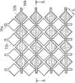
在本例中,电极由连接顶点的菱形物组成,以形成水平和垂直感测电极。In this example, the electrodes consist of rhombuses connecting vertices to form horizontal and vertical sensing electrodes.
上述电极形成笔直电极线20a和20b,其包括沿着电极线的菱形部分22a和22b。菱形部分22a和22b的节距(pitch)(意即菱形部分中心之间的距离)与其它阵列的电极线的节距相同,以便定义出规则阵列。The electrodes described above form straight electrode lines 20a and 20b, which include diamond-shaped portions 22a and 22b along the electrode lines. The pitch of the rhombic portions 22a and 22b (ie the distance between the centers of the rhombic portions) is the same as the pitch of the electrode lines of the other arrays so as to define a regular array.
上述电极的面积实质上较图1大,因而导致较高且更易于量测的电容值。The area of the above-mentioned electrodes is substantially larger than that in FIG. 1 , thus resulting in a higher and more measurable capacitance.
在本例中,感测元件与矩阵显示装置的结合处,感测电极的数量可能会低于显示装置中像素的行和列的数量,但是当物体位于感测电极中心之间的中间位置时,可以使用内插技术(interpolation technique)以测定物体的位置。In this example, where the sensing element is combined with the matrix display device, the number of sensing electrodes may be lower than the number of rows and columns of pixels in the display device, but when the object is located in the middle between the centers of the sensing electrodes , an interpolation technique can be used to determine the position of the object.
当感测电极结构位于矩阵显示装置的光学路径(optical path)中时,会发生位于显示装置表面上方的感测电极的图案可能会因亮度变化而被看见的问题。举例来说,铟锡氧化物(ITO)的导电层可典型具有95%的穿透率。人眼可以看出仅1%的亮度变化,所以当感测电极图案为线性或反复的结构的情况下,当使用者在观看荧幕时会看见感测电极图案。特别是观看移动影像的时候,感测电极的存在会降低显示影像的品质。When the sensing electrode structure is located in the optical path of the matrix display device, a problem occurs that the pattern of the sensing electrodes located above the surface of the display device may be visible due to brightness changes. For example, a conductive layer of indium tin oxide (ITO) may typically have a transmittance of 95%. Human eyes can see only 1% brightness variation, so when the sensing electrode pattern is a linear or repeated structure, the user will see the sensing electrode pattern when viewing the screen. Especially when watching moving images, the existence of the sensing electrodes will reduce the quality of the displayed images.
另一个问题是,当被感测的物体明显小于感测电极的节距时会影响物体位置的电容值的变化,当物体位于感测电极其中之一的中心时,会难以确定物体的位置。Another problem is that when the object being sensed is significantly smaller than the pitch of the sensing electrodes, the change in capacitance value affects the position of the object, making it difficult to determine the position of the object when the object is centered on one of the sensing electrodes.
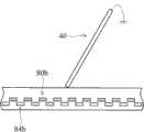
举例来说,图3为显示感测电极布局的一部分,而图4为显示其剖面图。For example, FIG. 3 shows a part of the layout of the sensing electrodes, and FIG. 4 shows a cross-sectional view thereof.
图3为显示沿着一行电极行的中心的线X-X。当触控物40位于如图4所示的线X-X的中心时(位于行方向感测电极32b和30b的其中之一的菱形部分的中间位置),会对行方向(水平方向)感测电极32b和30b(于后续的描述中会称为B电极)的电容值影响较大,但对邻近的列方向(垂直方向)感测电极30a和32a的电容值影响较小(于后续的描述中会称为A电极)。当触控物位于例如B电极的其它感测电极群组的其中之一的上方的中间位置时,会难以侦测位于例如A电极的感测电极群组的其中之一的触控的位置。触控物沿着列方向的移动对电容值的影响会远小于触控物沿着行方向的移动对电容值的影响。Fig. 3 shows a line X-X along the center of a row of electrodes. When the
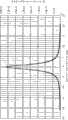
图5为显示当触控物对线X-X的中心的任一侧移动时,触控物与感测电极之间的电容估计值。曲线50显示触控物与B(行)电极之间的电容值,而曲线52和54显示触控物与位于两侧的A(列)电极之间的电容值。FIG. 5 shows the estimated capacitance between the touch object and the sensing electrode when the touch object moves to either side of the center of the line X-X.
就图5而言,触控物40的尖端直径为1mm,而菱形状的感测电极结构的侧边长度4.2mm(如图3所示的尺寸L)。Referring to FIG. 5 , the tip diameter of the
在图5中,x轴显示沿着线X-X的位置。位置0相当于菱形部分32b(如图4所示)的中间位置行方向感测电极(30a)。因此,这个位置对于行方向感测电极30b和32b具有电容最大值。当移动至一边时,对于行方向感测电极的电容值会下降(曲线50),但对于其中之一的列方向感测电极的电容值会增加(曲线52和54)。In Fig. 5, the x-axis shows the position along the line X-X.
当触控物40位于线X-X的中间位置时,触控物与邻近的A电极之间的电容会下降到低电容值,而大部分的电场位于触控物与感测电极之间,且终止在B感测电极。这样会难以侦测物体最靠近那一个A电极。When the
随物体位置变化的感测电极的电容值依感测电极的形状和尺寸而定。然而,符合想要的感测元件特性要求的电极图案会不同于符合最小化感测电极的可见度(visibility)要求的电极图案。当感测电极与显示器结合时,降低感测电极的可见度特别重要。The capacitance value of the sensing electrode that varies with the position of the object depends on the shape and size of the sensing electrode. However, electrode patterns that meet the requirements for desired sensing element characteristics may differ from electrode patterns that meet the requirements for minimizing the visibility of the sensing electrodes. Reducing the visibility of the sensing electrodes is particularly important when the sensing electrodes are combined with a display.
发明内容Contents of the invention
有鉴于此,本发明的实施例提供一种具有触控式感测输入元件的显示装置,其包括显示像素阵列或具有多个次像素群组的显示次像素阵列,该显示像素阵列和该显示次像素阵列共同定义各别的显示像素,该显示装置包括显示层;触控式感测输入元件,位于该显示层上方,该触控式感测输入元件使触控输入至该显示装置,其中该触控式感测输入元件包括第一电极阵列和第二电极阵列,其中在该第一电极阵列中的该多个电极与该第二电极阵列中的该多个电极正交;用于感测随现今的该触控输入变化的电极电容信号的电容感测排列结构,其中为了得到各别单独的感测信号而组合每一个该电极阵列的电极群组中的该电极电容信号,其中该第一电极阵列和该第二电极阵列的节距与该显示装置的像素节距或次像素节距相等。In view of this, an embodiment of the present invention provides a display device with a touch sensing input element, which includes a display pixel array or a display sub-pixel array with a plurality of sub-pixel groups, the display pixel array and the display The sub-pixel arrays jointly define respective display pixels, and the display device includes a display layer; a touch sensing input element is located above the display layer, and the touch sensing input element enables touch input to the display device, wherein The touch sensing input element includes a first electrode array and a second electrode array, wherein the plurality of electrodes in the first electrode array are orthogonal to the plurality of electrodes in the second electrode array; used for sensing A capacitive sensing arrangement structure for measuring electrode capacitive signals that vary with the current touch input, wherein the electrode capacitive signals in each electrode group of the electrode array are combined in order to obtain individual sensing signals, wherein the The pitch of the first electrode array and the second electrode array is equal to the pixel pitch or sub-pixel pitch of the display device.
这种排列方式使电极具有较感测分辨率细微的分辨率。每一个感测电极为各别电极的组合。可利用插入具有较感测电极排列结构小的几何形状且连接在一起的次电极以定义感测电极的方式形成上述感测电极结构。在这种方式中,感测电极排列结构与物体之间感测到的电场会在感测电极排列结构之间更均匀地分布,其中感测电极排列结构是侦测当物体靠近感测元件表面的特定区域时的位置。This arrangement allows the electrodes to have a finer resolution than the sensing resolution. Each sensing electrode is a combination of individual electrodes. The sensing electrode structure described above may be formed by inserting sub-electrodes having a smaller geometry than the sensing electrode arrangement and connected together to define the sensing electrodes. In this way, the electric field sensed between the sensing electrode arrangement and the object will be more evenly distributed among the sensing electrode arrangement, wherein the sensing electrode arrangement detects when the object approaches the surface of the sensing element. location in a specific area of .
本发明可更容易确认触控输入的位置。The present invention can more easily confirm the position of the touch input.
为了最小化感测电极排列结构的可见度,是利用感测电极的节距与显示器中像素或次像素的节距匹配的方式选择次电极节距的重复周期,使其等于显示器中像素节距的重复周期。In order to minimize the visibility of the sensing electrode arrangement structure, the repetition period of the sub-electrode pitch is chosen to be equal to the pixel pitch of the display in such a way that the pitch of the sensing electrodes matches the pitch of the pixels or sub-pixels in the display. repeat cycle.
优选地,一些电极(位于一个或两个电极阵列)作为虚设电极,上述虚设电极不为任何电极群组使用,因而不用以得到任何各别的感测信号。在这种方式中,可以选择想要的电极组合以形成感测信号,因而使感测电极产生的视觉影响愈小愈好,上述想要的电极组合不会破坏感测电极的规则图案。Preferably, some electrodes (in one or two electrode arrays) are used as dummy electrodes, which are not used by any electrode group and thus not used to obtain any individual sensing signal. In this way, the desired combination of electrodes can be selected to form the sensing signal, so that the visual impact of the sensing electrodes is as small as possible, and the desired combination of electrodes will not disrupt the regular pattern of the sensing electrodes.
在实施例中,每一个电极群组包括邻近的电极群组。意谓实际上每个感测电极的电极排列结构有效地延伸成为高分辨率电极阵列区域。因此高分辨率电极可视为次电极。因为这些次电极具有较感测分辨率细微的分辨率(举例来说,较被侦测物体尺寸细微的分辨率),当用来输入的物体移动时,从一个感测电极到下一个感测电极会有渐进的电容值变化。然而,上述感测电极排列结构仍会占据小的面积,因此可以最小化触控式感测元件在其下方的显示装置影像输出处的效应。当输入位置位于感测电极排列结构所在位置之间时,会有较强的触控式感测电容信号。In an embodiment, each electrode group includes adjacent electrode groups. It means that actually the electrode arrangement structure of each sensing electrode effectively extends into a high-resolution electrode array area. The high-resolution electrodes can therefore be regarded as sub-electrodes. Because these sub-electrodes have a finer resolution than the sensing resolution (for example, a finer resolution than the size of the detected object), when the object used for input moves, the The electrodes will have a gradual change in capacitance value. However, the above sensing electrode arrangement structure still occupies a small area, so the effect of the touch sensing element on the image output of the display device below it can be minimized. When the input position is located between the positions of the sensing electrode arrangement structure, there will be a stronger touch sensing capacitive signal.
在另一实施例中,每一个电极群组包括没有邻近电极区块的电极群组。在本例中,可将次电极连接在一起形成感测电极,以便在感测电极和物体侦测位置产生想要的电容关联。在本例中,可以使感测电极的输出信号最佳化。In another embodiment, each electrode group includes electrode groups with no adjacent electrode blocks. In this case, the sub-electrodes can be connected together to form the sensing electrodes to create the desired capacitive correlation between the sensing electrodes and the object detection location. In this example, the output signal of the sensing electrodes can be optimized.
举例来说,可由不同次电极得到的不同的感测信号。有些电极可不用于测得任何各别的感测信号。然而,仍可提供这些不使用的电极以使次电极能定义出规则阵列。For example, different sensing signals can be obtained from different sub-electrodes. Some electrodes may not be used to measure any respective sense signal. However, these unused electrodes can still be provided so that the sub-electrodes can define a regular array.
举例来说,每一个电极阵列可包括笔直的电极线,上述电极线具有沿着电极线的放大部分,上述放大部分的间距对应于其它阵列的电极线之间的节距。上述间距为定义放大部分的阵列,且会增加电容值。上述放大部分可为菱形。两个电极阵列可具有相同的节距。For example, each electrode array may include straight electrode lines with enlarged portions along the electrode lines, the intervals of the enlarged portions corresponding to the pitches between electrode lines of other arrays. The above pitches define the array of enlarged sections and will increase the capacitance value. The aforesaid enlarged part may be in the shape of a rhombus. Both electrode arrays may have the same pitch.
本发明实施例的显示装置可包括彩色滤光片排列结构,且电极的节距可与彩色滤光片图案的节距(对应于次像素节距)相等。The display device of the embodiment of the present invention may include a color filter arrangement structure, and the pitch of the electrodes may be equal to the pitch of the color filter pattern (corresponding to the sub-pixel pitch).
因此,在使用彩色滤光片的有源矩阵显示器的实施例中,次电极的重复周期与彩色滤光片图案的重复周期相等。彩色滤光片阵列可位于显示层和触控式感测输入元件之间。Thus, in an embodiment of an active matrix display using color filters, the repetition period of the sub-electrodes is equal to the repetition period of the color filter pattern. A color filter array may be located between the display layer and the touch-sensing input element.
上述触控式感测输入元件可包括位于第一电极阵列和第二电极阵列之间的玻璃基板,以及位于第二电极阵列上方的抗刮涂层,其中上述第二电极阵列位于玻璃基板和显示层相邻侧的相反侧。上述显示层可包括液晶层。The touch sensing input element may include a glass substrate between the first electrode array and the second electrode array, and an anti-scratch coating on the second electrode array, wherein the second electrode array is located between the glass substrate and the display The side opposite to the adjacent side of the layer. The above-mentioned display layer may include a liquid crystal layer.
以下以各实施例详细说明并伴随着附图说明的范例,做为本发明的参考依据。Hereinafter, each embodiment is described in detail and examples accompanied by accompanying drawings are used as a reference basis of the present invention.
附图说明Description of drawings
图1为已知触控式感测元件的电极的第一排列结构。FIG. 1 is a first arrangement structure of electrodes of a known touch sensing element.
图2为另一已知触控式感测元件的电极的第二排列结构。FIG. 2 is a second arrangement structure of electrodes of another known touch sensing element.
图3为图2的一部分,其用以解释图2排列结构的问题。FIG. 3 is a part of FIG. 2 , which is used to explain the problem of the arrangement structure in FIG. 2 .
图4显示输入元件与触控式感测元件如何互相作用,其用以解释图2排列结构的问题。FIG. 4 shows how the input element interacts with the touch sensing element, which is used to explain the problem of the arrangement shown in FIG. 2 .
图5用以解释图2排列结构的问题。Figure 5 is used to explain the problem of the arrangement structure in Figure 2.
图6为可应用于本发明实施例的具有触控式感测输入元件的已知显示装置结构。FIG. 6 is a structure of a known display device with a touch sensing input element applicable to an embodiment of the present invention.
图7为本发明实施例的触控式感测元件的电极的第一排列结构。FIG. 7 is a first arrangement structure of electrodes of the touch sensing element according to the embodiment of the present invention.
图8为本发明实施例的触控式感测元件的电极的第二排列结构。FIG. 8 is a second arrangement structure of electrodes of the touch sensing element according to the embodiment of the present invention.
图9为图8的一部分,其用以解释本发明的优点。Fig. 9 is a part of Fig. 8, which is used to explain the advantages of the present invention.
图10显示输入元件与触控式感测元件如何互相作用,其用以解释本发明的优点。FIG. 10 shows how the input element interacts with the touch sensing element, which is used to explain the advantages of the present invention.
图11用以解释本发明的优点。Figure 11 is used to explain the advantages of the present invention.
图12定义本发明实施例的感测电极的节距。Figure 12 defines the pitch of the sensing electrodes of an embodiment of the present invention.
图13显示本发明实施例的感测电极的节距如何可与彩色滤光片的排列结构匹配。FIG. 13 shows how the pitch of the sensing electrodes according to the embodiment of the present invention can match the arrangement structure of the color filters.
图14显示介于触控物和单一基板之间的电容如何随触控物与次电极的中心的距离变化。Figure 14 shows how the capacitance between a stylus and a single substrate varies with the distance of the stylus from the center of the sub-electrode.
图15显示本发明实施例的次电极群组,上述次电极群组不以邻近的次电极群组为基础。FIG. 15 shows a sub-electrode group according to an embodiment of the present invention, which is not based on adjacent sub-electrode groups.
图16为触控物位置的电容目标曲线,以及利用图15所示的次电极群组量测的电容近似曲线。FIG. 16 is a capacitance target curve at the position of the touch object, and an approximate curve of capacitance measured using the sub-electrode group shown in FIG. 15 .
图17显示为了形成一组感测电极,而使如图15所示的一些次电极群组可以彼此平行的方式设置。FIG. 17 shows that in order to form a set of sensing electrodes, some sub-electrode groups as shown in FIG. 15 can be arranged parallel to each other.
图18为利用图17的三个邻近的感测电极的物体位置特性和电容的关系。FIG. 18 is an object position characteristic versus capacitance using three adjacent sensing electrodes of FIG. 17 .
附图标记说明Explanation of reference signs
10a、10b~电极; 20a、20b、30a、30b~笔直电极线;10a, 10b~electrodes; 20a, 20b, 30a, 30b~straight electrode lines;
22a、22b、32a、32b~菱形部分;40~触控物;22a, 22b, 32a, 32b~rhombic part; 40~touch object;
60~部分的显示装置; 62~共用电极;60~Part of the display device; 62~Common electrodes;
64~彩色滤光片层; 68~Y感测电极排列结构;64~color filter layer; 68~Y sensing electrode arrangement structure;
66~平面介电层; 70~基板;66~planar dielectric layer; 70~substrate;
72~X感测电极排列结构; 74~偏光层-抗刮层;72~X sensing electrode arrangement structure; 74~polarizing layer-anti-scratch layer;
76~触控物; 80a、80b~水平B电极;76~touch object; 80a, 80b~horizontal B electrode;
84a、84b~垂直A电极; 82a、82b、86a、86b~群组;84a, 84b~vertical A electrodes; 82a, 82b, 86a, 86b~groups;
50、52、54、110、112、114、116、160、162、180a、180b、180c~曲线;50, 52, 54, 110, 112, 114, 116, 160, 162, 180a, 180b, 180c~curve;
PSUB_A、PSUB_B、PRGBH、PRGBV~节距。PSUB_A , PSUB_B , PRGBH , PRGBV ~pitch.
具体实施方式Detailed ways
在附图或说明书描述中,相似或相同的部分皆使用相同的图号。且在附图中,实施例的形状或是厚度可扩大,并以简化或是方便标示。再者,附图中各元件的部分将以分别描述说明,值得注意的是,图中未绘示或描述的元件,为所属技术领域中普通技术人员所知的形式,另外,特定的实施例仅为揭示本发明使用的特定方式,其并非用以限定本发明。In the drawings or descriptions in the specification, the same reference numerals are used for similar or identical parts. And in the drawings, the shapes or thicknesses of the embodiments may be enlarged, and marked for simplicity or convenience. Furthermore, the parts of each element in the drawings will be described separately. It should be noted that the elements not shown or described in the drawings are forms known to those of ordinary skill in the art. In addition, specific embodiments It is only used to disclose the specific method used in the present invention, and it is not intended to limit the present invention.
本发明实施例提供触控式感测输入元件,其中的电容感测电极排列为连接的电极群组,以使各别电极的间距小于感测分辨率的间距。上述触控式感测输入元件可改善使用于所有位置的触控式感测输入元件的量测位置单一性的能力。上述较小的电极节距与显示装置的设计匹配,以降低电容感测电极结构造成的伪影(visual artifact)问题。An embodiment of the present invention provides a touch sensing input element, wherein the capacitive sensing electrodes are arranged as connected electrode groups, so that the distance between the respective electrodes is smaller than the distance between the sensing resolutions. The touch-sensing input element described above can improve the ability to measure the singleness of the touch-sensing input element used in all positions. The smaller electrode pitch described above matches the design of the display device to reduce the problem of visual artifacts caused by the capacitive sensing electrode structure.
在描述本发明之前,提供可应用于本发明实施例的显示装置。图6为可应用于本发明实施例的具有电容触控式感测输入元件的已知显示装置结构。Before describing the present invention, a display device applicable to an embodiment of the present invention is provided. FIG. 6 is a structure of a known display device with a capacitive touch sensing input element applicable to an embodiment of the present invention.
元件符号60表示部分的显示装置,部分的显示装置60包括至少一显示层。在本发明实施例中,显示面板的精确设计并非本发明的重要技术特征,因而在此不做详细说明。典型地,上述显示装置的结构为液晶显示器,其包括夹设于基板间的液晶材料层。对于有源矩阵显示器而言,上述基板包括下方的薄膜晶体管阵列基板和上方的彩色滤光片基板。举例来说,彩色滤光片基板包括共用电极62。共用电极62为利用透明导电层形成的共用接地面,其位于彩色滤光片层64上。位于共用电极62下方的液晶层61设置于薄膜晶体管阵列基板上。
平面介电层66和用于触控式感测元件的Y感测电极排列结构68位于彩色滤光片层64上方。A
实际上,共用电极62、彩色滤光片64、平面介电层66和Y感测电极排列结构68设置于基板70上。因此,上述(顶)基板70雷同于液晶显示器支撑结构彩色滤光片基板,可做为触控式感测元件的支撑结构。Actually, the
X感测电极排列结构72位于基板70和Y感测电极排列结构68邻近侧的相对侧,且偏光层-抗刮层74用来做上表面。上述元件(抗刮层74)用于液晶显示器触控式荧幕的已知层,可以做为使用者触控互动碰触抗刮层的表面,其中使用者有可能是以触控物76或手指76来碰触。The X
因此,图6为显示显示装置结构,其上方具有触控式感测元件。例如玻璃基板70、偏光层-抗刮层74和彩色滤光片层64的显示结构的一些元件可与触控式感测元件整合。因此,上述显示装置结构不具有个别定义的显示部分和触控式感测元件部分。然而,一般显示功能(光的产生或光的调节)位于一般的触控式感测功能的下方,因此可以了解说明书的描述和权利要求。Therefore, FIG. 6 shows the structure of a display device with a touch sensing element above it. Some elements of the display structure such as
图6仅显示一种可能的整合结构。进一步的整合将X感测电极排列结构72移入显示器中(位于基板之间)。然而,上述进一步的整合会降低触控物对X感测电极和Y感测电极的电容的影响程度。图6为显示将触控式感测元件整合于显示装置结构中的第一步骤,本发明应用相同的设计,但将触控式感测功能与显示功能做进一步的整合。Figure 6 shows only one possible integration structure. Further integration moves the
图7和图8为显示用于图1和图2所示的感测电极结构的建议排列方法的第一种排列结构。在上述实施例中,以四个次电极连接形成的群组做为每一个感测电极的结构,然而其它实施例也可使用更多数量的次电极连接形成的群组做为每一个感测电极的结构。可利用如图7和图8所示的电性连接的方式做为群组中次电极之间的连接方式。FIGS. 7 and 8 are a first arrangement structure showing a suggested arrangement method for the sensing electrode structures shown in FIGS. 1 and 2 . In the above-mentioned embodiment, the group formed by four sub-electrode connections is used as the structure of each sensing electrode, but other embodiments can also use a group formed by a greater number of sub-electrode connections as the structure of each sensing electrode. Electrode structure. The electrical connections shown in FIG. 7 and FIG. 8 can be used as the connection between the sub-electrodes in the group.
图7和图8所示的次电极的结构类似于原来的感测电极,但原来的感测电极则不需用于本实施例中。可通过电性连接的方式使位于感测区周围的邻近的次电极形成感测电极。可利用垂直A电极84a或84b的电容值来测得物体的水平位置和水平B电极80a或80b的电容值来测得物体的垂直位置的方式来测得物体的位置。The structures of the sub-electrodes shown in FIG. 7 and FIG. 8 are similar to the original sensing electrodes, but the original sensing electrodes are not used in this embodiment. Adjacent sub-electrodes around the sensing region can form sensing electrodes by being electrically connected. The position of the object can be detected by using the capacitance value of the
图7为显示个别的条状水平(行)电极80a,上述水平电极80a连接形成群组82a。每一个水平电极可视为次电极,而每一个群组82a可视为组合的感测电极排列结构。同样地,个别的垂直(列)电极84a连接形成群组86a。FIG. 7 shows individual strip-shaped horizontal (row)
图8为显示个别的具有菱形物(如图2所示)的条状水平(行)电极80b,上述水平电极80b又连接形成群组82b。而个别的具有菱形物(如图2所示)的条形垂直(列)电极84b又连接形成群组86b。FIG. 8 shows individual strip-shaped horizontal (row)
图9、10、11为显示使用次电极的优点。Figures 9, 10 and 11 show the advantages of using sub-electrodes.
图9为显示图8感测电极排列结构的放大部分,以及沿着模拟触控物移动路径的线X-X。图10为感测电极排列结构的剖面图,其显示触控物40和个别的水平电极80b和垂直电极84b。FIG. 9 is an enlarged portion showing the arrangement structure of the sensing electrodes in FIG. 8 , and the line X-X along the moving path of the simulated touch object. FIG. 10 is a cross-sectional view of the sensing electrode arrangement structure, which shows the
图11为显示触控物与感测电极排列结构之间的量测电容如何随着触控物40(如图10所示)沿着如图9所示的线X-X的位置变化。FIG. 11 shows how the measured capacitance between the touch object and the sensing electrode arrangement varies with the position of the touch object 40 (shown in FIG. 10 ) along the line X-X shown in FIG. 9 .
当触控物沿着线X-X的位置变化时,如曲线110所示,触控物与水平电极形成的群组82b(行感测电极排列结构)之间的电容值并没有明显的变化。而三个连续的垂直电极形成的群组86b(垂直感测电极排列结构)的电容值平缓地变化,且上述垂直电极形成的群组86b的至少一个在所有的位置中具有明显的电容值。曲线112、114和116为上述三个邻近的垂直电极形成的群组86b(垂直感测电极排列结构)的电容值。When the position of the touch object along the line X-X changes, as shown by the
图12为显示次电极图案的水平方向的重复间距PSUB_A和次电极图案的垂直方向的重复间距PSUB_B。当电极于显示装置之前方形成时,次电极的节距与显示装置的像素的重复节距匹配。因而对所有像素具有相同的影响,降低伪影的产生。FIG. 12 is a diagram showing the repeat pitch PSUB_A of the sub-electrode pattern in the horizontal direction and the repeat pitch PSUB_B of the sub-electrode pattern in the vertical direction. When the electrodes are formed in front of the display device, the pitch of the sub-electrodes matches the repeating pitch of the pixels of the display device. Therefore, all pixels have the same effect, reducing the generation of artifacts.
图13为显示有源距阵显示器的彩色像素的一种可能的布局(layout),其具有水平方向的重复间距PRGBH和垂直方向的重复间距PRGBV。上述彩色像素以红(R)像素列、绿(G)像素列和蓝(B)像素列的方式排列。为了将电容感测电极的可见度最小化,应使次电极图案和显示装置的像素的重复间距匹配,所以PSUB_A=PRGBH且PSUB_B=PRGBV。FIG. 13 shows a possible layout of color pixels of an active matrix display, which has a repeat pitch PRGBH in the horizontal direction and a repeat pitch PRGBV in the vertical direction. The color pixels are arranged in a red (R) pixel column, a green (G) pixel column and a blue (B) pixel column. In order to minimize the visibility of the capacitive sensing electrodes, the sub-electrode pattern and the repeat pitch of the pixels of the display device should be matched, soPSUB_A =PRGBH andPSUB_B =PRGBV .
在上述实施例中,相邻的次电极形成群组。在其它实施例中,可为了调整电容感测元件的特性而改变次电极群组的形成方式,意即电容感测元件量测的电容随着例如尺寸和位置的被感测物体特性而变。In the above embodiments, adjacent sub-electrodes form a group. In other embodiments, the formation of the sub-electrode groups can be varied in order to adjust the characteristics of the capacitive sensing element, ie the capacitance measured by the capacitive sensing element varies with the characteristics of the sensed object such as size and position.
为了说明上述的其它实施例,使用基于介于感测电极和例如触控物或手指的被感测物体的电容量测(相对于感测电极之间的电容量测)做为考量的感测元件。上述次电极可以排列为如图1和图2所示的格子图案。当例如接地导电触控物的物体接近于其中之一的感测电极时,会增加感测电极与物体之间的电容值。图14为显示触控物与单一次电极(single sub-electrode)之间的电容如何随着触控物与位于垂直于次电极的轴线上的次电极的中心的相对位置变化。To illustrate the other embodiments described above, use sensing based on consideration of the capacitance measurement between the sensing electrodes and the sensed object, such as a stylus or finger (as opposed to capacitance measurement between the sensing electrodes). element. The above-mentioned sub-electrodes may be arranged in a grid pattern as shown in FIG. 1 and FIG. 2 . When an object such as a grounded conductive touch object approaches one of the sensing electrodes, the capacitance between the sensing electrode and the object increases. FIG. 14 shows how the capacitance between the touch object and a single sub-electrode varies with the relative position of the touch object and the center of the sub-electrode on the axis perpendicular to the sub-electrode.
当触控物朝着次电极移动时,电容值会增加。当触控物位于次电极的正上方时,电容值会达到峰值。在本例中,次电极的宽度约为0.1mm,而触控物的直径为1.5mm。When the touch object moves towards the sub-electrode, the capacitance value will increase. When the touch object is directly above the sub-electrode, the capacitance value will reach a peak value. In this example, the width of the sub-electrode is about 0.1 mm, and the diameter of the touch object is 1.5 mm.
邻近的次电极相对于偏移一段距离的触控物位置的电容值会有类似的变化,其中偏移距离对应于次电极的间隔。每一个感测电极可利用电性连接上述各别的次电极群组形成。之后,可利用计算群组中次电极的电容值的总和,得到感测电极与触控物之间的电容值变化,其中触控物与感测电极的中心具有相对位置。The capacitance of adjacent sub-electrodes will have a similar change with respect to the position of the touch object offset by a distance, wherein the offset distance corresponds to the spacing of the sub-electrodes. Each sensing electrode can be formed by electrically connecting the above-mentioned respective sub-electrode groups. Afterwards, the capacitance value change between the sensing electrode and the touch object can be obtained by calculating the sum of the capacitance values of the sub-electrodes in the group, wherein the centers of the touch object and the sensing electrode have relative positions.
图15显示本发明实施例的次电极群组,上述次电极群组不以邻近的次电极群组为基础,而以一组次电极替代,以得到想要的电容值。图15中的次电极以相对于位于中心的次电极来编号,其中位于右侧的次电极以正值标示,位于左侧的次电极以负值标示。FIG. 15 shows a sub-electrode group according to an embodiment of the present invention. The above-mentioned sub-electrode group is not based on an adjacent sub-electrode group, but is replaced by a group of sub-electrodes to obtain a desired capacitance value. The sub-electrodes in FIG. 15 are numbered relative to the sub-electrode located in the center, wherein the sub-electrode located on the right is indicated with a positive value, and the sub-electrode located on the left is indicated with a negative value.
中心位于次电极0的感测电极利用连接次电极+3、-3、+19、-19、+20、-20、+22和-22形成。如图16所示,感测电极与触控物之间的电容变化依触控物与次电极0的相对位置而定。A sensing electrode centered on
在图16中,曲线160表示触控物位置的电容值目标曲线,而曲线162显示利用图15所示的次电极群组量测的电容近似曲线。由上述可知,利用适当地将次电极分组的方式可实质上调整感测电极的特性。In FIG. 16 ,
为了感测物体在区域上方的位置,必须使用多重感测电极(multiple senseelectrode)。图17为显示为了形成一组感测电极,而使一些次电极群组可以彼此平行的方式设置。在本例中,感测电极的间距为次电极间距的30倍。因此,次电极的间距远比感测分辨率更为狭窄。感测电极的节距决定感测分辨率。另外,次电极群组彼此部分重叠。可以从图17中清楚地看出,每一个感测电极利用多个次电极横跨一定的宽度,且上述宽度大于感测电极之间的距离。In order to sense the position of an object over the area, multiple sense electrodes must be used. FIG. 17 shows that in order to form a set of sensing electrodes, some sub-electrode groups can be arranged in parallel with each other. In this example, the distance between the sensing electrodes is 30 times the distance between the sub-electrodes. Therefore, the pitch of the sub-electrodes is much narrower than the sensing resolution. The pitch of the sensing electrodes determines the sensing resolution. In addition, the sub-electrode groups partially overlap each other. It can be clearly seen from FIG. 17 that each sensing electrode utilizes a plurality of sub-electrodes across a certain width, and the aforementioned width is greater than the distance between the sensing electrodes.
对于这种特定的次电极群组图案和感测电极间距,可使次电极不需成为一个以上群组的一部分。For this particular sub-electrode group pattern and sensing electrode spacing, the sub-electrodes need not be part of more than one group.
然而,在其它实施例中。可利用不同群组之间的次电极在时间多路传输(multiplex)或结合从次电极传来的数据以在信号处理阶段形成虚拟群组的方式,使次电极可用于多重感测电极中。上述情形会在后续讨论。这些量测表示次电极可为两个不同感测电极的一部分,不是因为结合不同时间的次电极信号以形成不同的感测电极信号,就是因为利用信号处理方式得到感测电极信号(会于后续描述)。However, in other embodiments. Sub-electrodes can be used in multiple sensing electrodes by time multiplexing sub-electrodes between different groups or combining data from sub-electrodes to form virtual groups during signal processing. The above situation will be discussed later. These measurements indicate that the sub-electrodes can be part of two different sensing electrodes, either because the sub-electrode signals at different times are combined to form different sensing electrode signals, or because the sensing electrode signals are derived using signal processing (discussed later in describe).
图18为显示如图17所示的三个邻近的感测电极随物体位置变化的电容量测结果。每一个感测电容的电容值曲线180a、180b和180c的形状相同,但沿水平轴线位置偏移,其偏移量等于感测电容的间距。FIG. 18 is a graph showing capacitance measurement results of three adjacent sensing electrodes as shown in FIG. 17 as a function of object position. The capacitance curves 180a, 180b and 180c of each sensing capacitor have the same shape, but are shifted along the horizontal axis by an amount equal to the distance between the sensing capacitors.
经由编组次电极产生的随物体位置变化的电容曲线的实施例纯粹用于说明。事实上,可由例如将感测电极得到的信号的信噪比(signal to noise ratio)最大化或简化转换感测电极数据对物体位置需要的信号处理等标准选择电容曲线和编组次电极。The example of capacitance curves as a function of object position via grouping of sub-electrodes is purely for illustration. In fact, the capacitance curve and grouping of the sub-electrodes can be selected by criteria such as maximizing the signal to noise ratio of the signal obtained by the sensing electrodes or simplifying the signal processing required to convert the sensing electrode data to the object position.
在编组次电极的实施例中,形成群组的次电极的图案呈中心对称。然而其它实施例中,形成群组的次电极的图案可不对称。举例来说,感测元件的区域上方的次电极群组的图案具有变化是有益的。举例来说,为了保证感测区域的边缘被截断的感测电极群组仍具有一致的性能,接近边缘的次电极群组可使用不同的图案。In the embodiment of grouping the sub-electrodes, the pattern of the sub-electrodes forming the group is symmetrical about the center. However, in other embodiments, the pattern of the sub-electrodes forming the group may be asymmetric. For example, it is beneficial to have variations in the pattern of the sub-electrode groups over the area of the sensing element. For example, in order to ensure that the sense electrode group whose edge is truncated in the sensing region still has consistent performance, the sub-electrode group near the edge can use a different pattern.
可能会有一些不用于感测物体的次电极,这是因为上述次电极不包含在感测电极群组。虽然这些次电极不用于感测,但这些次电极仍可存在。这是为了要通过使感测元件各处区域的电极图案均一,而使感测电极的能见度降低。这些次电极可做为虚设电极。There may be some sub-electrodes that are not used for sensing objects because the above-mentioned sub-electrodes are not included in the sensing electrode group. Although these sub-electrodes are not used for sensing, these sub-electrodes can still be present. This is to reduce the visibility of the sensing electrodes by making the electrode pattern uniform across the sensing element. These sub-electrodes can be used as dummy electrodes.
如上所述,位于与显示器结合的感测元件位置的均一且重复的图案与显示器相匹配。然而,为了最小化感测用的次电极量测时产生的任何干扰或破坏,应该电处理上述不使用的次电极。在大多数情形下,意谓上述不使用的次电极应连接至低阻抗元件,举例来说,上述不使用的次电极可以接地。As described above, the uniform and repeating pattern at the location of the sensing elements associated with the display matches the display. However, in order to minimize any interference or damage to the measurement of the sensing sub-electrodes, the unused sub-electrodes should be electrically treated. In most cases, it means that the above-mentioned unused sub-electrodes should be connected to a low-impedance element, for example, the above-mentioned unused sub-electrodes can be grounded.
对于具有邻近群组或没有邻近群组的次电极群组两者而言,上述实施例显示利用例如金属线或导线的导体做为次电极硬接线(hard wire)之间的连接,以将次电极连接成群组。在其它实施例中,可以经由电容或允许电荷通过群组中次电极之间的其它电子元件,以间接耦接群组中的次电极。For both groups of sub-electrodes with or without adjacent groups, the above-described embodiments show the use of conductors such as metal wires or wires as connections between the sub-electrodes hard wires to separate the sub-electrodes. The electrodes are connected in groups. In other embodiments, the sub-electrodes in the group may be coupled indirectly via capacitors or other electronic components that allow charges to pass between the sub-electrodes in the group.
另外,也可以连接虚设感测电极以虚拟方式形成群组的次电极。在本例中,群组中的次电极之间没有直接的电性连接。可以从各别的次电极或次电极的小群组(较形成感测电极所需次电极数量少的次电极形成的群组)中得到替代数据,且上述替代数据可于信号处理程序结合以得到可从次电极的全部群组数据表现的信号。因此,重点为结合次电极的群组的信号以形成感测电极的信号,且可经由直接连接或信号处理方式得到这种结合。因此,可排列上述元件,以使群组中并非所有次电极都直接连接在一起,且上述电极信号的结合是至少一部分应用于信号处理。In addition, dummy sensing electrodes can also be connected to form a group of sub-electrodes in a virtual manner. In this example, there is no direct electrical connection between the sub-electrodes in the group. Substitute data can be obtained from individual sub-electrodes or small groups of sub-electrodes (groups formed by fewer sub-electrodes than are required to form sensing electrodes), and the above-mentioned substitute data can be combined in signal processing to A signal representable from the entire group data of the sub-electrodes is obtained. Therefore, the emphasis is on combining the signals of groups of sub-electrodes to form the signals of the sensing electrodes, and this combination can be obtained through direct connection or signal processing. Accordingly, the elements may be arranged such that not all sub-electrodes in a group are directly connected together, and the combination of signals from the electrodes is at least partly used for signal processing.
优选可以同时量测次电极或次电极群组的电容值,以降低所有的量测时间。在其它实施例中,可用时间序列(time sequential)的方式量测次电极或次电极群组的电容值。Preferably, the capacitance values of the sub-electrodes or sub-electrode groups can be measured at the same time, so as to reduce the overall measurement time. In other embodiments, the capacitance of the sub-electrode or sub-electrode group can be measured in a time sequential manner.
使用已存在的已知的排列结构做为上述感测电容的排列结构在此不做详细描述。上述感测电容的排列结构不是用来感测一对电极之间的电容值,就是用来感测电极和接地触控物之间的电容值,其中每一个感测电极对的一个电极属于每一个电极阵列。Using an existing known arrangement structure as the arrangement structure of the sensing capacitors will not be described in detail here. The arrangement structure of the above-mentioned sensing capacitance is not used to sense the capacitance value between a pair of electrodes, or is used to sense the capacitance value between the electrode and the ground touch object, wherein one electrode of each sensing electrode pair belongs to each an electrode array.
本发明实施例是应用利用电容感测的触控式感测输入元件的电容值量测,特别是应用于例如有源式矩阵液晶显示器(AMLCD)或有源矩阵有机发光二极管显示器(AMOLED)的阵列显示器。Embodiments of the present invention are applied to capacitance value measurement of a touch-sensing input element using capacitive sensing, especially for active matrix liquid crystal display (AMLCD) or active matrix organic light emitting diode display (AMOLED). array display.
上述电极的节距优选与次像素节距(红(R)、绿(G)、蓝(B)次像素的节距)相同。然而,上述电极的节距可与所有像素的节距相同,每一个像素均一影响。当然,有些显示器可以没有次像素。举例来说,彩色序列显示器可以时序方式对不同色彩使用相同的像素。The pitch of the electrodes is preferably the same as the sub-pixel pitch (the pitch of the red (R), green (G), blue (B) sub-pixels). However, the pitch of the above-mentioned electrodes may be the same as that of all pixels, and each pixel is uniformly affected. Of course, some displays do not have sub-pixels. For example, a color sequential display can use the same pixels for different colors in a time-sequential manner.
在一些实施例中,用以形成一条感测线的电极群组可延伸跨越大量数目的次电极。举例来说,位于中心次电极线的每一侧至少三个、五个或八个次电极。In some embodiments, a group of electrodes used to form a sensing line can extend across a large number of sub-electrodes. For example, at least three, five or eight sub-electrodes are located on each side of the central sub-electrode line.
虽然本发明已以实施例披露如上,然其并非用以限定本发明,任何本领域一般技术人员,在不脱离本发明的精神和范围内,当可作些许的更动与润饰,因此本发明的保护范围当视所附的权利要求所界定为准。Although the present invention has been disclosed above with embodiments, it is not intended to limit the present invention. Any person skilled in the art may make some changes and modifications without departing from the spirit and scope of the present invention. Therefore, the present invention The scope of protection shall prevail as defined by the appended claims.
Claims (10)
Translated fromChineseApplications Claiming Priority (6)
| Application Number | Priority Date | Filing Date | Title |
|---|---|---|---|
| US12596308P | 2008-04-30 | 2008-04-30 | |
| US12591708P | 2008-04-30 | 2008-04-30 | |
| US61/125,917 | 2008-04-30 | ||
| US61/125,963 | 2008-04-30 | ||
| EP09152695.4 | 2009-02-12 | ||
| EP09152695.4AEP2113827B8 (en) | 2008-04-30 | 2009-02-12 | Touch input device |
Publications (2)
| Publication Number | Publication Date |
|---|---|
| CN101571781Atrue CN101571781A (en) | 2009-11-04 |
| CN101571781B CN101571781B (en) | 2013-11-20 |
Family
ID=40904677
Family Applications (1)
| Application Number | Title | Priority Date | Filing Date |
|---|---|---|---|
| CN2009101358380AActiveCN101571781B (en) | 2008-04-30 | 2009-04-29 | Display device |
Country Status (5)
| Country | Link |
|---|---|
| US (2) | US20090273572A1 (en) |
| EP (1) | EP2113827B8 (en) |
| JP (2) | JP2009271923A (en) |
| CN (1) | CN101571781B (en) |
| TW (1) | TWI460494B (en) |
Cited By (22)
| Publication number | Priority date | Publication date | Assignee | Title |
|---|---|---|---|---|
| CN101943814A (en)* | 2010-07-16 | 2011-01-12 | 汕头超声显示器(二厂)有限公司 | Built-in touch-control liquid crystal display |
| CN102193669A (en)* | 2010-03-16 | 2011-09-21 | 乐金显示有限公司 | A touch panel and method of manufacturing the same |
| CN102214036A (en)* | 2010-04-02 | 2011-10-12 | 三星电子株式会社 | Method and apparatus for forming electrode pattern on touch panel |
| CN102314273A (en)* | 2010-06-30 | 2012-01-11 | 索尼公司 | Capacitive transducer and message input device |
| CN102339178A (en)* | 2010-07-28 | 2012-02-01 | 义隆电子股份有限公司 | Capacitive touch pad for improving linear response |
| CN102375636A (en)* | 2010-08-19 | 2012-03-14 | 索尼公司 | Display unit with touch detection function, and electronic device |
| CN102375638A (en)* | 2010-08-23 | 2012-03-14 | 索尼公司 | Display device with touch detection function, touch detection device, and electronic unit |
| CN102446023A (en)* | 2010-10-01 | 2012-05-09 | 群康科技(深圳)有限公司 | Touch sensing panels and operation method thereof, display apparatus and electric apparatus |
| CN103282866A (en)* | 2010-11-05 | 2013-09-04 | 富士胶片株式会社 | Touch panel |
| CN103294292A (en)* | 2012-03-27 | 2013-09-11 | 上海天马微电子有限公司 | Touch detection method of capacitive touch screen and capacitive touch screen |
| CN103902118A (en)* | 2012-12-24 | 2014-07-02 | 宏达国际电子股份有限公司 | Touch panel |
| CN103970384A (en)* | 2013-01-25 | 2014-08-06 | 原相科技股份有限公司 | Capacitive touch panel, sensing method thereof, touch device and input device |
| CN103970313A (en)* | 2013-01-25 | 2014-08-06 | 深圳欧菲光科技股份有限公司 | Touch inducing element and touch screen |
| CN104102399A (en)* | 2013-04-13 | 2014-10-15 | 贵州达沃斯光电有限公司 | Capacitive touch screen and manufacturing method thereof |
| CN104360773A (en)* | 2014-11-25 | 2015-02-18 | 上海天马微电子有限公司 | Touch display device and electronic equipment |
| CN104484084A (en)* | 2014-12-18 | 2015-04-01 | 合肥鑫晟光电科技有限公司 | Driving method of touch screen, touch screen and display device |
| US9379704B2 (en) | 2012-12-24 | 2016-06-28 | Htc Corporation | Touch panel |
| CN105892738A (en)* | 2014-05-09 | 2016-08-24 | Lg伊诺特有限公司 | Touch panel and image display device having the same |
| CN106203247A (en)* | 2014-08-20 | 2016-12-07 | 速博思股份有限公司 | Combined sensing fingerprint identification device and method |
| CN102375638B (en)* | 2010-08-23 | 2016-12-14 | 株式会社日本显示器 | There is the touch display device of detection function, touch detecting apparatus and electronic unit |
| CN107402657A (en)* | 2016-05-20 | 2017-11-28 | 乐金显示有限公司 | Perceive the touch-screen touched with fingerprint |
| CN109240553A (en)* | 2017-10-27 | 2019-01-18 | 上海飞智电子科技有限公司 | Touch device component and touch-control system |
Families Citing this family (50)
| Publication number | Priority date | Publication date | Assignee | Title |
|---|---|---|---|---|
| US8164343B2 (en) | 2003-09-05 | 2012-04-24 | Midtronics, Inc. | Method and apparatus for measuring a parameter of a vehicle electrical system |
| CN101382651B (en)* | 2007-09-07 | 2011-12-14 | 群康科技(深圳)有限公司 | Touch control type electric moisten display device, touch control type circuit base board and method for manufacturing same |
| KR100978461B1 (en)* | 2008-07-04 | 2010-08-26 | 안영수 | High Sensitivity Digital Capacitive Touch Panel Device |
| WO2010013679A1 (en)* | 2008-07-31 | 2010-02-04 | グンゼ株式会社 | Planar element, and touch switch |
| JP5287738B2 (en)* | 2009-03-16 | 2013-09-11 | 株式会社リコー | Information input apparatus, image forming apparatus, position determination method, and position determination program |
| KR20110091244A (en)* | 2010-02-05 | 2011-08-11 | 삼성모바일디스플레이주식회사 | Touch screen panel |
| FR2958422B1 (en)* | 2010-03-31 | 2012-06-08 | Valeo Systemes Thermiques | HUMAN MACHINE INTERFACE |
| TWI435140B (en)* | 2010-04-09 | 2014-04-21 | Wintek Corp | Display with touch panel |
| JP5396333B2 (en)* | 2010-05-17 | 2014-01-22 | パナソニック株式会社 | Touch panel device |
| TWI424197B (en)* | 2010-06-23 | 2014-01-21 | Chunghwa Picture Tubes Ltd | Touch panel for displaying stereoscopic image |
| TWI502452B (en) | 2010-07-26 | 2015-10-01 | Elan Microelectronics Corp | A capacitive touchpad that improves linear response |
| JP5260607B2 (en)* | 2010-09-01 | 2013-08-14 | 双葉電子工業株式会社 | Touch sensor and fluorescent display tube |
| CN101950230B (en)* | 2010-09-21 | 2012-02-22 | 友达光电股份有限公司 | Capacitive touch sensor and capacitive touch device |
| KR101230196B1 (en)* | 2010-10-29 | 2013-02-06 | 삼성디스플레이 주식회사 | Liquid Crystal Display having a Touch Screen Panel |
| US8970541B2 (en) | 2010-11-24 | 2015-03-03 | Innolux Corporation | Sensing devices |
| KR101219273B1 (en)* | 2011-01-14 | 2013-01-08 | 삼성디스플레이 주식회사 | touch screen system |
| CN102832209A (en)* | 2011-06-16 | 2012-12-19 | 联咏科技股份有限公司 | Capacitor array substrate |
| KR20130016980A (en) | 2011-08-09 | 2013-02-19 | 삼성디스플레이 주식회사 | Display device |
| KR101771609B1 (en) | 2011-09-21 | 2017-08-28 | 엘지디스플레이 주식회사 | method for sensing touch of touch panel |
| US20130127744A1 (en)* | 2011-11-22 | 2013-05-23 | Qualcomm Mems Technologies, Inc. | Wireframe touch sensor design and spatially linearized touch sensor design |
| JP5748647B2 (en)* | 2011-12-22 | 2015-07-15 | 富士フイルム株式会社 | Conductive sheet and touch panel |
| JP5777251B2 (en)* | 2011-12-16 | 2015-09-09 | 富士フイルム株式会社 | Conductive sheet for touch panel and touch panel |
| JP5509186B2 (en)* | 2011-12-16 | 2014-06-04 | 富士フイルム株式会社 | Touch panel and conductive sheet for touch panel |
| BR112014010102A8 (en) | 2011-12-16 | 2017-06-20 | Fujifilm Corp | electroconductive sheet and touch panel |
| KR101893111B1 (en) | 2012-01-04 | 2018-08-31 | 삼성디스플레이 주식회사 | Display device including sensor |
| KR101859662B1 (en)* | 2012-01-10 | 2018-05-18 | 삼성전자주식회사 | Touch sensor and touch panel including the same |
| TWI547851B (en)* | 2012-01-13 | 2016-09-01 | 聯詠科技股份有限公司 | Capacitive touch display device |
| KR101859515B1 (en) | 2012-02-14 | 2018-05-21 | 삼성디스플레이 주식회사 | Touch panel |
| US9081442B2 (en) | 2012-02-27 | 2015-07-14 | Apple Inc. | Split sense lines for negative pixel compensation |
| US9197208B2 (en) | 2012-04-19 | 2015-11-24 | Elo Touch Solutions, Inc. | Projected capacitive touch sensor with asymmetric bridge pattern |
| JP6355623B2 (en)* | 2012-04-19 | 2018-07-11 | イーロ・タッチ・ソリューションズ・インコーポレイテッド | Projection-type capacitive touch sensor with asymmetric bridge pattern |
| KR101944503B1 (en)* | 2012-06-21 | 2019-04-18 | 삼성디스플레이 주식회사 | Sensor substrate and sensing display panel having the same |
| US8872764B2 (en) | 2012-06-29 | 2014-10-28 | Qualcomm Mems Technologies, Inc. | Illumination systems incorporating a light guide and a reflective structure and related methods |
| US8773386B2 (en)* | 2012-08-09 | 2014-07-08 | Cypress Semiconductor Corporation | Methods and apparatus to scan a targeted portion of an input device to detect a presence |
| US9389737B2 (en) | 2012-09-14 | 2016-07-12 | Samsung Display Co., Ltd. | Display device and method of driving the same in two modes |
| US11314368B2 (en) | 2012-09-14 | 2022-04-26 | Samsung Display Co., Ltd. | Display device and method of driving the same in two modes |
| KR102040973B1 (en)* | 2012-12-14 | 2019-11-06 | 삼성디스플레이 주식회사 | Touch Screen Panel |
| CN103870044B (en)* | 2012-12-18 | 2017-01-11 | 宸鸿光电科技股份有限公司 | Touch electrode structure and manufacturing process thereof |
| KR102075040B1 (en) | 2013-02-05 | 2020-02-11 | 삼성디스플레이 주식회사 | Touch Screen Panel |
| CN104049816A (en)* | 2013-03-15 | 2014-09-17 | 北京京东方光电科技有限公司 | Plate electrode for capacitive touch screen, touch screen and touch display device |
| JP5865285B2 (en)* | 2013-03-27 | 2016-02-17 | 株式会社ジャパンディスプレイ | Display device with touch detection function and electronic device |
| JP2014191654A (en)* | 2013-03-27 | 2014-10-06 | Sharp Corp | Input device and electronic apparatus |
| JP5882538B2 (en) | 2013-04-18 | 2016-03-09 | シャープ株式会社 | Sensor sheet, sensor sheet module, touch sensor panel module, and electronic device |
| JP6199667B2 (en)* | 2013-09-11 | 2017-09-20 | 株式会社ジャパンディスプレイ | Organic electroluminescence device with input function |
| JP2015215800A (en)* | 2014-05-12 | 2015-12-03 | 株式会社ジャパンディスプレイ | Portable electronic device |
| JP2016126480A (en)* | 2014-12-26 | 2016-07-11 | 大日本印刷株式会社 | Touch panel sensor |
| JP6546943B2 (en)* | 2017-02-13 | 2019-07-17 | 株式会社ジャパンディスプレイ | Display with touch panel function |
| US10996781B2 (en)* | 2019-08-13 | 2021-05-04 | Wuhan China Star Optoelectronics Semiconductor Display Technology Co., Ltd. | Display panel and display device |
| JP7390246B2 (en)* | 2020-04-23 | 2023-12-01 | ルネサスエレクトロニクス株式会社 | Semiconductor device and character recognition method |
| US11893192B2 (en)* | 2021-06-18 | 2024-02-06 | Sensel, Inc. | Interpolation electrode patterning for capacitive-grid touch sensor |
Citations (3)
| Publication number | Priority date | Publication date | Assignee | Title |
|---|---|---|---|---|
| CN1942853A (en)* | 2004-05-06 | 2007-04-04 | 苹果电脑有限公司 | multi-touch screen |
| EP1837742A2 (en)* | 2006-03-22 | 2007-09-26 | Wacom Co., Ltd. | Display device, sensor panel, position-detecting device position-inputting device and computer system. |
| US20080062148A1 (en)* | 2006-06-09 | 2008-03-13 | Hotelling Steve P | Touch screen liquid crystal display |
Family Cites Families (35)
| Publication number | Priority date | Publication date | Assignee | Title |
|---|---|---|---|---|
| US4321567A (en)* | 1980-03-24 | 1982-03-23 | Raytheon Company | Combining series sections weighting with withdrawal weighting in SAW transducers |
| JPH01209521A (en)* | 1988-02-17 | 1989-08-23 | Pentel Kk | tablet input device |
| US5534892A (en)* | 1992-05-20 | 1996-07-09 | Sharp Kabushiki Kaisha | Display-integrated type tablet device having and idle time in one display image frame to detect coordinates and having different electrode densities |
| GB9406702D0 (en)* | 1994-04-05 | 1994-05-25 | Binstead Ronald P | Multiple input proximity detector and touchpad system |
| TW274598B (en)* | 1994-11-15 | 1996-04-21 | Alps Electric Co Ltd | Coordinate input device for pen of finger tip |
| US5650597A (en)* | 1995-01-20 | 1997-07-22 | Dynapro Systems, Inc. | Capacitive touch sensor |
| JPH09258893A (en)* | 1996-03-25 | 1997-10-03 | Toshiba Corp | Coordinate input device and input display device including the same |
| JP3434415B2 (en)* | 1996-07-05 | 2003-08-11 | アルプス電気株式会社 | Coordinate input device |
| JPH11110115A (en)* | 1997-09-30 | 1999-04-23 | Fujitsu General Ltd | Digitizer device |
| US6730863B1 (en)* | 1999-06-22 | 2004-05-04 | Cirque Corporation | Touchpad having increased noise rejection, decreased moisture sensitivity, and improved tracking |
| JP2003099185A (en)* | 2001-09-20 | 2003-04-04 | Alps Electric Co Ltd | Input device |
| US6825833B2 (en)* | 2001-11-30 | 2004-11-30 | 3M Innovative Properties Company | System and method for locating a touch on a capacitive touch screen |
| DE10237119B3 (en)* | 2002-08-13 | 2004-04-15 | Fujitsu Siemens Computers Gmbh | display device |
| TWI278690B (en)* | 2004-06-25 | 2007-04-11 | Hannstar Display Corp | Input-sensor-integrated liquid crystal display panel |
| DE112004002965A5 (en)* | 2004-10-06 | 2007-09-13 | Fraunhofer-Gesellschaft zur Förderung der angewandten Forschung e.V. | Apparatus and method for driving an organic light emitting diode |
| EP1892609A4 (en)* | 2005-05-26 | 2013-03-27 | Gunze Kk | Transparent planar body and transparent touch switch |
| US7864160B2 (en)* | 2005-10-05 | 2011-01-04 | 3M Innovative Properties Company | Interleaved electrodes for touch sensing |
| US7868874B2 (en)* | 2005-11-15 | 2011-01-11 | Synaptics Incorporated | Methods and systems for detecting a position-based attribute of an object using digital codes |
| US20070132737A1 (en)* | 2005-12-09 | 2007-06-14 | Mulligan Roger C | Systems and methods for determining touch location |
| KR101202588B1 (en)* | 2005-12-27 | 2012-11-19 | 엘지디스플레이 주식회사 | LCD and driving method thereof |
| JP4648860B2 (en)* | 2006-03-16 | 2011-03-09 | 株式会社ワコム | Position detection apparatus and computer |
| GB2439614B (en)* | 2006-05-31 | 2008-12-24 | Harald Philipp | Two-dimensional position sensor |
| CN102981678B (en)* | 2006-06-09 | 2015-07-22 | 苹果公司 | Touch screen liquid crystal display |
| JP2008116921A (en)* | 2006-10-10 | 2008-05-22 | Sony Corp | Display device and information processing apparatus |
| JP4153009B2 (en)* | 2007-02-15 | 2008-09-17 | アルプス電気株式会社 | Input device |
| JP4453710B2 (en)* | 2007-03-19 | 2010-04-21 | セイコーエプソン株式会社 | Liquid crystal device, electronic apparatus and position detection method |
| JP2008281616A (en)* | 2007-05-08 | 2008-11-20 | Seiko Epson Corp | Liquid crystal device and electronic device |
| US20080297174A1 (en)* | 2007-05-31 | 2008-12-04 | Sarangan Narasimhan | Capacitive sensing devices |
| US20080309633A1 (en)* | 2007-06-13 | 2008-12-18 | Apple Inc. | Touch-sensitive display |
| CN101158764A (en)* | 2007-11-07 | 2008-04-09 | 昆山龙腾光电有限公司 | LCD panel, display apparatus and touch sensing switch |
| EP2113828B1 (en)* | 2008-04-30 | 2017-10-11 | InnoLux Corporation | Display device with touch screen |
| KR100957836B1 (en)* | 2008-06-02 | 2010-05-14 | 주식회사 애트랩 | Touch panel device and its contact position detection method |
| US9395850B2 (en)* | 2008-10-06 | 2016-07-19 | Japan Display Inc. | Coordinate input device and display device with the same |
| US20100214247A1 (en)* | 2009-02-20 | 2010-08-26 | Acrosense Technology Co., Ltd. | Capacitive Touch Panel |
| US8681119B2 (en)* | 2010-09-27 | 2014-03-25 | Blackberry Limited | Electronic device and touch-sensitive input device |
- 2009
- 2009-02-12EPEP09152695.4Apatent/EP2113827B8/enactiveActive
- 2009-04-29CNCN2009101358380Apatent/CN101571781B/enactiveActive
- 2009-04-29TWTW098114196Apatent/TWI460494B/ennot_activeIP Right Cessation
- 2009-04-30JPJP2009111347Apatent/JP2009271923A/enactivePending
- 2009-04-30USUS12/433,513patent/US20090273572A1/ennot_activeAbandoned
- 2013
- 2013-11-22JPJP2013241782Apatent/JP2014032707A/enactivePending
- 2015
- 2015-11-30USUS14/954,818patent/US10042451B2/enactiveActive
Patent Citations (3)
| Publication number | Priority date | Publication date | Assignee | Title |
|---|---|---|---|---|
| CN1942853A (en)* | 2004-05-06 | 2007-04-04 | 苹果电脑有限公司 | multi-touch screen |
| EP1837742A2 (en)* | 2006-03-22 | 2007-09-26 | Wacom Co., Ltd. | Display device, sensor panel, position-detecting device position-inputting device and computer system. |
| US20080062148A1 (en)* | 2006-06-09 | 2008-03-13 | Hotelling Steve P | Touch screen liquid crystal display |
Cited By (47)
| Publication number | Priority date | Publication date | Assignee | Title |
|---|---|---|---|---|
| US8947370B2 (en) | 2010-03-16 | 2015-02-03 | Lg Display Co., Ltd. | Touch panel and method for manufacturing the same |
| CN102193669A (en)* | 2010-03-16 | 2011-09-21 | 乐金显示有限公司 | A touch panel and method of manufacturing the same |
| CN102214036A (en)* | 2010-04-02 | 2011-10-12 | 三星电子株式会社 | Method and apparatus for forming electrode pattern on touch panel |
| CN102314273A (en)* | 2010-06-30 | 2012-01-11 | 索尼公司 | Capacitive transducer and message input device |
| CN101943814A (en)* | 2010-07-16 | 2011-01-12 | 汕头超声显示器(二厂)有限公司 | Built-in touch-control liquid crystal display |
| CN101943814B (en)* | 2010-07-16 | 2012-07-18 | 汕头超声显示器(二厂)有限公司 | Built-in touch-control liquid crystal display |
| CN102339178A (en)* | 2010-07-28 | 2012-02-01 | 义隆电子股份有限公司 | Capacitive touch pad for improving linear response |
| CN102375636A (en)* | 2010-08-19 | 2012-03-14 | 索尼公司 | Display unit with touch detection function, and electronic device |
| US10162470B2 (en) | 2010-08-19 | 2018-12-25 | Japan Display Inc. | Display unit with touch detection function, and electronic device |
| CN102375636B (en)* | 2010-08-19 | 2015-12-16 | 株式会社日本显示器 | There is the display unit and electronic installation that touch measuring ability |
| US9122359B2 (en) | 2010-08-19 | 2015-09-01 | Japan Display Inc. | Display unit with touch detection function, and electronic device |
| US9619098B2 (en) | 2010-08-19 | 2017-04-11 | Japan Display Inc. | Display unit with touch detection function, and electronic device |
| US10386984B2 (en) | 2010-08-19 | 2019-08-20 | Japan Display Inc. | Display unit with touch detection function, and electronic device |
| US10365745B2 (en) | 2010-08-23 | 2019-07-30 | Japan Display Inc. | Display device with touch detection function, touch detection device, and electronic unit |
| US10061418B2 (en) | 2010-08-23 | 2018-08-28 | Japan Display Inc. | Display device with touch detection function, touch detection device, and electronic unit |
| US9606661B2 (en) | 2010-08-23 | 2017-03-28 | Japan Display Inc. | Display device with touch detection function, touch detection device, and electronic unit |
| US9081447B2 (en) | 2010-08-23 | 2015-07-14 | Japan Display Inc. | Display device with touch detection function, touch detection device, and electronic unit |
| CN102375638A (en)* | 2010-08-23 | 2012-03-14 | 索尼公司 | Display device with touch detection function, touch detection device, and electronic unit |
| CN102375638B (en)* | 2010-08-23 | 2016-12-14 | 株式会社日本显示器 | There is the touch display device of detection function, touch detecting apparatus and electronic unit |
| CN102446023B (en)* | 2010-10-01 | 2015-04-08 | 群康科技(深圳)有限公司 | Touch sensing panels and operation method thereof, display apparatus and electric apparatus |
| CN102446023A (en)* | 2010-10-01 | 2012-05-09 | 群康科技(深圳)有限公司 | Touch sensing panels and operation method thereof, display apparatus and electric apparatus |
| CN103282866A (en)* | 2010-11-05 | 2013-09-04 | 富士胶片株式会社 | Touch panel |
| CN103282866B (en)* | 2010-11-05 | 2016-10-26 | 富士胶片株式会社 | touch panel |
| CN103294292B (en)* | 2012-03-27 | 2016-12-14 | 上海天马微电子有限公司 | Touch detection method of capacitive touch screen and capacitive touch screen |
| CN103294292A (en)* | 2012-03-27 | 2013-09-11 | 上海天马微电子有限公司 | Touch detection method of capacitive touch screen and capacitive touch screen |
| US9379704B2 (en) | 2012-12-24 | 2016-06-28 | Htc Corporation | Touch panel |
| CN103902118B (en)* | 2012-12-24 | 2017-04-26 | 宏达国际电子股份有限公司 | touch panel |
| CN103902118A (en)* | 2012-12-24 | 2014-07-02 | 宏达国际电子股份有限公司 | Touch panel |
| CN103970384A (en)* | 2013-01-25 | 2014-08-06 | 原相科技股份有限公司 | Capacitive touch panel, sensing method thereof, touch device and input device |
| CN103970313A (en)* | 2013-01-25 | 2014-08-06 | 深圳欧菲光科技股份有限公司 | Touch inducing element and touch screen |
| CN104102399A (en)* | 2013-04-13 | 2014-10-15 | 贵州达沃斯光电有限公司 | Capacitive touch screen and manufacturing method thereof |
| CN104102399B (en)* | 2013-04-13 | 2017-12-05 | 贵州达沃斯光电有限公司 | Capacitive touch screen and preparation method thereof |
| CN105892738B (en)* | 2014-05-09 | 2019-12-13 | Lg伊诺特有限公司 | Touch panel and image display device having the touch panel |
| US10227600B2 (en) | 2014-05-09 | 2019-03-12 | Lg Innotek Co., Ltd. | Touch panel and image display device having the same |
| CN105892738A (en)* | 2014-05-09 | 2016-08-24 | Lg伊诺特有限公司 | Touch panel and image display device having the same |
| CN106203247A (en)* | 2014-08-20 | 2016-12-07 | 速博思股份有限公司 | Combined sensing fingerprint identification device and method |
| CN106203247B (en)* | 2014-08-20 | 2019-06-14 | 速博思股份有限公司 | Combined sensing fingerprint identification device and method |
| CN104360773A (en)* | 2014-11-25 | 2015-02-18 | 上海天马微电子有限公司 | Touch display device and electronic equipment |
| CN107024792A (en)* | 2014-11-25 | 2017-08-08 | 上海天马微电子有限公司 | Touch display device and electronic equipment |
| CN104360773B (en)* | 2014-11-25 | 2017-07-07 | 上海天马微电子有限公司 | Touch display device and electronic equipment |
| CN107024792B (en)* | 2014-11-25 | 2020-04-24 | 上海天马微电子有限公司 | Touch display device and electronic equipment |
| US9965084B2 (en) | 2014-12-18 | 2018-05-08 | Boe Technology Group Co., Ltd. | Driving method of touch screen, touch screen and display apparatus |
| CN104484084A (en)* | 2014-12-18 | 2015-04-01 | 合肥鑫晟光电科技有限公司 | Driving method of touch screen, touch screen and display device |
| CN107402657A (en)* | 2016-05-20 | 2017-11-28 | 乐金显示有限公司 | Perceive the touch-screen touched with fingerprint |
| CN107402657B (en)* | 2016-05-20 | 2020-05-01 | 乐金显示有限公司 | Touchscreen that senses touch and fingerprints |
| CN109240553A (en)* | 2017-10-27 | 2019-01-18 | 上海飞智电子科技有限公司 | Touch device component and touch-control system |
| CN109240553B (en)* | 2017-10-27 | 2024-04-19 | 上海飞智电子科技有限公司 | Touch device assembly and touch system |
Also Published As
| Publication number | Publication date |
|---|---|
| JP2014032707A (en) | 2014-02-20 |
| TW200944877A (en) | 2009-11-01 |
| EP2113827B8 (en) | 2018-09-19 |
| CN101571781B (en) | 2013-11-20 |
| EP2113827A2 (en) | 2009-11-04 |
| JP2009271923A (en) | 2009-11-19 |
| EP2113827B1 (en) | 2018-08-01 |
| EP2113827A3 (en) | 2012-09-12 |
| US10042451B2 (en) | 2018-08-07 |
| US20160085350A1 (en) | 2016-03-24 |
| TWI460494B (en) | 2014-11-11 |
| US20090273572A1 (en) | 2009-11-05 |
Similar Documents
| Publication | Publication Date | Title |
|---|---|---|
| CN101571781A (en) | Display device | |
| US10496223B2 (en) | Touch detection device and display device with touch detection function | |
| JP6549976B2 (en) | Touch detection device and display device with touch detection function | |
| US9417748B2 (en) | Input device and display device | |
| KR101461925B1 (en) | Touch detecting apparatuse for improving visualbility | |
| EP2556423B1 (en) | Equalizing parasitic capacitance effects in touch screens | |
| TWI516834B (en) | Proximity detection device, method of detecting proximity and electronic apparatus | |
| US9274653B2 (en) | Touch detection device and display device having touch sensor function | |
| US9097928B2 (en) | Capacitive touch panel and display device | |
| JP2017162173A (en) | Detection device, display device, and electronic apparatus | |
| KR20150091248A (en) | Display device provided with sensor and method of driving the same | |
| CN104662502A (en) | Liquid crystal display device | |
| CN104049801A (en) | Touch control display panel, driving method, and touch control display device | |
| CN104898911A (en) | In cell touch panel and display device | |
| JP2015195010A (en) | Input device having touch sensor function and display device | |
| WO2014045602A1 (en) | Display device | |
| US10216340B2 (en) | Touch detection device for improving touch detection and visibility and electronic device comprising same | |
| KR101461928B1 (en) | Touch detecting apparatuse for improving visualbility | |
| KR101707391B1 (en) | Touch detecting apparatus for hybrid scan type touch detecting | |
| WO2014045600A1 (en) | Liquid crystal display device | |
| KR20180069280A (en) | Multi point touch screen pannel | |
| KR20180069283A (en) | Multi point touch screen pannel | |
| KR20150025832A (en) | Touch detecting apparatuse for improving touch detecting | |
| KR20150109891A (en) | Touch detecting three dimensional display apparatus featuring graded size slits |
Legal Events
| Date | Code | Title | Description |
|---|---|---|---|
| C06 | Publication | ||
| PB01 | Publication | ||
| C10 | Entry into substantive examination | ||
| SE01 | Entry into force of request for substantive examination | ||
| ASS | Succession or assignment of patent right | Owner name:QIMEI ELECTRONIC CO LTD Free format text:FORMER OWNER: TONGBAO OPTOELECTRONICS CO., LTD. Effective date:20131009 | |
| C41 | Transfer of patent application or patent right or utility model | ||
| C53 | Correction of patent of invention or patent application | ||
| CB02 | Change of applicant information | Address after:Hsinchu Science Park, Taiwan, China Applicant after:INNOLUX DISPLAY CORP. Address before:Miaoli County, Taiwan, China Applicant before:CHI MEI OPTOELECTRONICS CORP. | |
| COR | Change of bibliographic data | Free format text:CORRECT: APPLICANT; FROM: QIMEI ELECTRONIC CO LTD TO: INNOLUX DISPLAY CORPORATION | |
| TA01 | Transfer of patent application right | Effective date of registration:20131009 Address after:Miaoli County, Taiwan, China Applicant after:CHI MEI OPTOELECTRONICS CORP. Address before:Hsinchu science industry zone, Taiwan, China Applicant before:TOPPOLY OPTOELECTRONICS Corp. | |
| C14 | Grant of patent or utility model | ||
| GR01 | Patent grant |