CN101569000B - Substrate heat-treating apparatus, and substrate heat-treating method - Google Patents
Substrate heat-treating apparatus, and substrate heat-treating methodDownload PDFInfo
- Publication number
- CN101569000B CN101569000BCN2008800011475ACN200880001147ACN101569000BCN 101569000 BCN101569000 BCN 101569000BCN 2008800011475 ACN2008800011475 ACN 2008800011475ACN 200880001147 ACN200880001147 ACN 200880001147ACN 101569000 BCN101569000 BCN 101569000B
- Authority
- CN
- China
- Prior art keywords
- substrate
- heat
- substrate stage
- heat dissipation
- stage
- Prior art date
- Legal status (The legal status is an assumption and is not a legal conclusion. Google has not performed a legal analysis and makes no representation as to the accuracy of the status listed.)
- Active
Links
Images


Classifications
- H—ELECTRICITY
- H01—ELECTRIC ELEMENTS
- H01L—SEMICONDUCTOR DEVICES NOT COVERED BY CLASS H10
- H01L21/00—Processes or apparatus adapted for the manufacture or treatment of semiconductor or solid state devices or of parts thereof
- H01L21/67—Apparatus specially adapted for handling semiconductor or electric solid state devices during manufacture or treatment thereof; Apparatus specially adapted for handling wafers during manufacture or treatment of semiconductor or electric solid state devices or components ; Apparatus not specifically provided for elsewhere
- H01L21/67005—Apparatus not specifically provided for elsewhere
- H01L21/67011—Apparatus for manufacture or treatment
- H01L21/67098—Apparatus for thermal treatment
- H01L21/67115—Apparatus for thermal treatment mainly by radiation
- H—ELECTRICITY
- H01—ELECTRIC ELEMENTS
- H01L—SEMICONDUCTOR DEVICES NOT COVERED BY CLASS H10
- H01L21/00—Processes or apparatus adapted for the manufacture or treatment of semiconductor or solid state devices or of parts thereof
- H01L21/67—Apparatus specially adapted for handling semiconductor or electric solid state devices during manufacture or treatment thereof; Apparatus specially adapted for handling wafers during manufacture or treatment of semiconductor or electric solid state devices or components ; Apparatus not specifically provided for elsewhere
- H01L21/683—Apparatus specially adapted for handling semiconductor or electric solid state devices during manufacture or treatment thereof; Apparatus specially adapted for handling wafers during manufacture or treatment of semiconductor or electric solid state devices or components ; Apparatus not specifically provided for elsewhere for supporting or gripping
- H01L21/687—Apparatus specially adapted for handling semiconductor or electric solid state devices during manufacture or treatment thereof; Apparatus specially adapted for handling wafers during manufacture or treatment of semiconductor or electric solid state devices or components ; Apparatus not specifically provided for elsewhere for supporting or gripping using mechanical means, e.g. chucks, clamps or pinches
- H01L21/68714—Apparatus specially adapted for handling semiconductor or electric solid state devices during manufacture or treatment thereof; Apparatus specially adapted for handling wafers during manufacture or treatment of semiconductor or electric solid state devices or components ; Apparatus not specifically provided for elsewhere for supporting or gripping using mechanical means, e.g. chucks, clamps or pinches the wafers being placed on a susceptor, stage or support
- H01L21/68785—Apparatus specially adapted for handling semiconductor or electric solid state devices during manufacture or treatment thereof; Apparatus specially adapted for handling wafers during manufacture or treatment of semiconductor or electric solid state devices or components ; Apparatus not specifically provided for elsewhere for supporting or gripping using mechanical means, e.g. chucks, clamps or pinches the wafers being placed on a susceptor, stage or support characterised by the mechanical construction of the susceptor, stage or support
- H—ELECTRICITY
- H01—ELECTRIC ELEMENTS
- H01L—SEMICONDUCTOR DEVICES NOT COVERED BY CLASS H10
- H01L21/00—Processes or apparatus adapted for the manufacture or treatment of semiconductor or solid state devices or of parts thereof
- H01L21/02—Manufacture or treatment of semiconductor devices or of parts thereof
- H01L21/04—Manufacture or treatment of semiconductor devices or of parts thereof the devices having potential barriers, e.g. a PN junction, depletion layer or carrier concentration layer
- H01L21/0445—Manufacture or treatment of semiconductor devices or of parts thereof the devices having potential barriers, e.g. a PN junction, depletion layer or carrier concentration layer the devices having semiconductor bodies comprising crystalline silicon carbide
Landscapes
- Engineering & Computer Science (AREA)
- Physics & Mathematics (AREA)
- Condensed Matter Physics & Semiconductors (AREA)
- General Physics & Mathematics (AREA)
- Manufacturing & Machinery (AREA)
- Computer Hardware Design (AREA)
- Microelectronics & Electronic Packaging (AREA)
- Power Engineering (AREA)
- Health & Medical Sciences (AREA)
- Toxicology (AREA)
- Container, Conveyance, Adherence, Positioning, Of Wafer (AREA)
- Tunnel Furnaces (AREA)
Abstract
Description
Translated fromChinese技术领域technical field
本发明涉及一种用于对衬底(例如,碳化硅(SiC)衬底)进行热处理的设备。更具体地,本发明涉及一种能够在真空中对衬底均匀且快速地进行热处理的设备以及一种使用该设备对衬底进行热处理的方法。The present invention relates to an apparatus for thermally treating a substrate, for example a silicon carbide (SiC) substrate. More particularly, the present invention relates to an apparatus capable of uniformly and rapidly heat-treating a substrate in a vacuum and a method of heat-treating a substrate using the apparatus.
背景技术Background technique
作为对衬底进行热处理的设备,已知的一种是:在该设备中,加热板布置在真空腔的下部处,环形冷却单元布置在真空腔的上部处,并且由具有高导热系数的材料制成的衬底支架布置在加热板与冷却单元之间以可竖直地运动(例如,参见专利文献1)。当利用该设备热处理衬底时,其上布置衬底的衬底支架向下运动。衬底支架的下表面与加热板接触以通过衬底支架加热衬底。然后,衬底支架向上运动以使衬底支架的周边与冷却单元接触,由此通过衬底支架冷却衬底。作为与加热板非接触地对衬底进行热处理的设备,已知的一种是:该设备设有冷却部分和在高温下加热衬底的气密反应腔(例如,参加专利文献2)。专利文献1:日本专利特开No.2003-318076专利文献2:日本专利特开No.2005-299990As an apparatus for heat-treating a substrate, there is known one in which a heating plate is arranged at the lower portion of the vacuum chamber, an annular cooling unit is arranged at the upper portion of the vacuum chamber, and a material having a high thermal conductivity The produced substrate holder is arranged between a heating plate and a cooling unit so as to be vertically movable (for example, see Patent Document 1). When a substrate is thermally treated with this apparatus, the substrate holder on which the substrate is placed moves downward. The lower surface of the substrate holder is in contact with a heating plate to heat the substrate by the substrate holder. Then, the substrate holder moves upward to bring the periphery of the substrate holder into contact with the cooling unit, thereby cooling the substrate through the substrate holder. As an apparatus for heat-treating a substrate in non-contact with a heating plate, there is known one that is provided with a cooling section and an airtight reaction chamber that heats a substrate at a high temperature (see, for example, Patent Document 2). Patent Document 1: Japanese Patent Laid-Open No. 2003-318076 Patent Document 2: Japanese Patent Laid-Open No. 2005-299990
发明内容Contents of the invention
在专利文献1中所说明的衬底热处理设备以及用于对衬底进行热处理的方法通过经由衬底支架的热传导来执行加热。因此,如果衬底和衬底支架没有相互均匀地接触,则在加热中可能出现不均匀性。例 如,如果衬底通过注入和加热过程被翘曲,则其可能与衬底支架局部接触或不接触。这就使作为加热之后的热处理特性的表面均匀度降级。由于衬底由衬底支架的周边冷却,整个衬底的温度不能均匀地降低。此外,通过其中心冷却衬底是花费时间的。The substrate heat treatment apparatus and the method for heat treating a substrate described in
在根据专利文献2的衬底热处理设备中,衬底通过辐射热被加热至高温。期望的是更有效地均匀加热衬底。即使在将衬底加热到高温时,温度也不应传导至腔壁。由于专利文献2的衬底处理设备利用冷却部分的壁进行冷却,必须保留较大的空间用于冷却部分。这使设备笨重。In the substrate heat treatment apparatus according to
本发明是考虑到上述传统问题而作出的,并且第一目的是提供一种可以在真空中均匀且快速地加热衬底的衬底热处理设备和衬底热处理方法。本发明的第二目的是提供一种可以快速冷却所加热衬底的整个部分的衬底热处理设备和衬底热处理方法。本发明的第三目的是提供一种可以小型化的衬底热处理设备以及使用该设备对衬底进行热处理的方法。The present invention has been made in consideration of the above conventional problems, and a first object is to provide a substrate heat treatment apparatus and a substrate heat treatment method that can uniformly and rapidly heat a substrate in a vacuum. A second object of the present invention is to provide a substrate heat treatment apparatus and a substrate heat treatment method capable of rapidly cooling the entire portion of a heated substrate. A third object of the present invention is to provide a substrate heat treatment apparatus that can be miniaturized and a method for heat treating a substrate using the apparatus.
一种解决上述目的至少之一、根据本发明的衬底热处理设备是这样一种衬底热处理设备,所述设备包括:包括衬底台架的衬底支架单元,衬底布置在所述衬底台架上,且所述衬底台架由碳或覆盖有碳的材料制成,设置在所述衬底台架上方的加热单元,所述加热单元包括与所述衬底台架相对的散热表面,并用来自所述散热表面的辐射热与布置在所述衬底台架上的所述衬底非接触地加热所述衬底,腔,衬底支架单元和加热单元布置在所述腔中,以及升降装置,其使所述衬底支架单元和所述加热单元中至少之一在所述腔中竖直地运动以使所述衬底台架和所述加热单元的散热表面相互接近或相互间隔开,其中所述衬底支架单元包括:辐射板,所述辐射板与所述衬底台架有间隙地布置在所述衬底台架下方,捕获从所述衬底台架的下表面发射的热,并朝所述衬底台架辐射所捕获的热,以及 反射板,所述反射板与所述辐射板有间隙地布置在所述辐射板下方,并反射从所述辐射板发射的热。A substrate heat treatment apparatus according to the present invention which solves at least one of the above objects is a substrate heat treatment apparatus comprising: a substrate holder unit including a substrate stage, a substrate is arranged on the substrate On the stage, and the substrate stage is made of carbon or a material covered with carbon, a heating unit is arranged above the substrate stage, and the heating unit includes a heat dissipation device opposite to the substrate stage surface, and heat the substrate non-contactingly with the substrate arranged on the substrate stage with radiant heat from the heat dissipation surface, a chamber, a substrate holder unit and a heating unit are arranged in the chamber , and a lifting device that moves at least one of the substrate holder unit and the heating unit vertically in the chamber so that the heat dissipation surfaces of the substrate stage and the heating unit approach each other or are spaced apart from each other, wherein the substrate holder unit includes: a radiating plate disposed below the substrate stage with a gap between the substrate stage and capturing radiation from the substrate stage below. heat emitted from the surface and radiates the captured heat toward the substrate stage, and a reflector plate disposed below the radiant plate with a gap therebetween and reflects the heat from the radiant plate Emitted heat.
一种根据本发明用于对衬底进行热处理的方法是使用这样一种衬底热处理设备对衬底进行热处理,所述设备包括:包括衬底台架的衬底支架单元,衬底布置在所述衬底台架上,和设置在所述衬底台架上方的加热单元,所述加热单元包括与所述衬底台架相对的散热表面,并用来自所述散热表面的辐射热与布置在所述衬底台架上的所述衬底非接触地加热所述衬底,所述方法包括:布置步骤,在所述衬底台架上布置其表面中具有注入区域的衬底,使得所述衬底在注入区域侧的表面面对所述加热单元的散热表面侧;热处理步骤,使用根据本发明的上述衬底热处理设备对衬底进行热处理。A method for heat-treating a substrate according to the present invention is to heat-treat a substrate using a substrate heat-treating apparatus comprising: a substrate holder unit comprising a substrate stage on which the substrate is arranged On the substrate stage, and a heating unit arranged above the substrate stage, the heating unit includes a heat dissipation surface opposite to the substrate stage, and uses the radiant heat from the heat dissipation surface and the heating unit arranged on the substrate stage The substrate on the substrate stage heats the substrate without contact, the method comprising the step of arranging a substrate having implanted regions in its surface on the substrate stage such that the The surface of the substrate on the injection region side faces the heat dissipation surface side of the heating unit; and in the heat treatment step, the substrate is heat treated using the above substrate heat treatment equipment according to the present invention.
根据本发明的衬底热处理设备以及对衬底进行热处理的方法用来自加热单元的散热表面的辐射热与衬底非接触地加热衬底。加热单元的散热表面与其中布置有衬底的衬底台架相对,并且其辐射热可以均匀地照射衬底,而不管衬底是否翘曲。因此,即使衬底或多或少地翘曲,该衬底也可以被均匀地加热。A substrate heat treatment apparatus and a method of heat treating a substrate according to the present invention heat the substrate non-contact with the substrate using radiant heat from the heat dissipation surface of the heating unit. The heat dissipation surface of the heating unit is opposed to the substrate stage in which the substrate is arranged, and its radiant heat can uniformly irradiate the substrate regardless of whether the substrate is warped or not. Therefore, even if the substrate is more or less warped, the substrate can be uniformly heated.
衬底台架由碳或覆盖有碳的材料制成。衬底台架的至少表面由具有高辐射率的碳制成。因此,衬底也同时地接收来自通过辐射加热的衬底台架的辐射热。即,衬底主要由来自加热单元的散热表面的辐射热加热,并且次要地由来自衬底台架的辐射热加热。因而,衬底可以快速地加热。The substrate stage is made of carbon or a material covered with carbon. At least the surface of the substrate stage is made of carbon with high emissivity. Accordingly, the substrate also simultaneously receives radiant heat from the substrate stage heated by radiation. That is, the substrate is mainly heated by radiant heat from the heat dissipation surface of the heating unit, and secondarily by radiant heat from the substrate stage. Thus, the substrate can be heated rapidly.
衬底台架的至少表面由具有高辐射率的碳制成。在冷却期间,当辐射热被吸收时,整个衬底台架的温度可以均匀且快速地降低。因此,衬底台架可以均匀且快速地冷却。At least the surface of the substrate stage is made of carbon with high emissivity. During cooling, when radiant heat is absorbed, the temperature of the entire substrate stage can be lowered uniformly and rapidly. Therefore, the substrate stage can be cooled uniformly and rapidly.
附图说明Description of drawings
包含在本说明书中且构成本说明书的一部分的附图示出了本 发明的实施例,并与说明书一起用于解释本发明的原理。图1是根据本发明一个实施例衬底热处理设备的示意性剖视图,示出在衬底装载/卸载期间的状态;图2是示出衬底加热期间的状态的示意性剖视图;图3是示出衬底冷却期间的状态的示意性剖视图;图4是图1中的衬底支架单元及其周边的放大剖视图;图5是图2中的衬底支架单元及其周边的放大剖视图;图6A是解释衬底台架的视图;图6B是解释衬底台架的视图;图6C是解释衬底台架的视图;图7是示例3中制造的p+n结二极管的剖视图;图8是示出示例3中制造的p+n结二极管的电流密度-电压特性的热处理温度依赖性的图表;以及图9是示出升降轴12的内部结构的透视图。The accompanying drawings, which are incorporated in and constitute a part of this specification, illustrate embodiments of the invention and together with the description serve to explain the principles of the invention. 1 is a schematic cross-sectional view of a substrate heat treatment apparatus according to an embodiment of the present invention, showing a state during substrate loading/unloading; FIG. 2 is a schematic cross-sectional view showing a state during substrate heating; FIG. A schematic cross-sectional view of a state during substrate cooling; FIG. 4 is an enlarged cross-sectional view of the substrate holder unit and its surroundings in FIG. 1; FIG. 5 is an enlarged cross-sectional view of the substrate holder unit and its surroundings in FIG. 2; FIG. 6A is a view for explaining a substrate stage; FIG. 6B is a view for explaining a substrate stage; FIG. 6C is a view for explaining a substrate stage; FIG. A graph showing the heat treatment temperature dependence of the current density-voltage characteristic of the p+ n junction diode manufactured in Example 3; and FIG. 9 is a perspective view showing the internal structure of the
具体实施方式Detailed ways
以下将详细说明本发明的实施例。应注意,这些实施例中说明的构成成分仅是示例。本发明的技术范围通过权利要求确定而不受以下各实施例限制。Embodiments of the present invention will be described in detail below. It should be noted that the constituent components described in these embodiments are only examples. The technical scope of the present invention is determined by the claims and is not limited by the following embodiments.
图1示出根据本发明一个实施例衬底热处理设备。图1是示出衬底装载/卸载期间的状态的示意性剖视图,图2是示出衬底加热期间的状态的示意性剖视图,以及图3是示出衬底冷却期间的状态的示意性剖视图。图4是图1中的衬底支架单元及其周边的放大剖视图,图5是图2中的衬底支架单元及其周边的放大剖视图,并且图6包括多个解释衬底台架的视图。应注意,在图1至6A、6B和6C中,相同的附图标记表示同样的构件或部分。FIG. 1 shows an apparatus for thermally treating a substrate according to one embodiment of the present invention. 1 is a schematic sectional view showing a state during substrate loading/unloading, FIG. 2 is a schematic sectional view showing a state during substrate heating, and FIG. 3 is a schematic sectional view showing a state during substrate cooling. . 4 is an enlarged cross-sectional view of the substrate holder unit and its periphery in FIG. 1 , FIG. 5 is an enlarged cross-sectional view of the substrate holder unit and its periphery in FIG. 2 , and FIG. 6 includes views for explaining substrate stages. It should be noted that in FIGS. 1 to 6A, 6B, and 6C, the same reference numerals denote the same members or parts.
如图1至3中所示,根据本实施例的衬底热处理设备,衬底支架单元A、加热单元B和挡板装置C布置在真空腔D中。As shown in FIGS. 1 to 3 , according to the substrate heat treatment apparatus of the present embodiment, a substrate holder unit A, a heating unit B, and a baffle device C are arranged in a vacuum chamber D. As shown in FIG.
衬底支架单元A包括在其最靠上部分处的衬底台架1。加热单 元B布置在衬底台架1上方并且包括与衬底台架1相对的散热表面2。通过升降装置E可以使衬底支架单元A竖直地运动。可以通过升降装置E的操作控制衬底台架1和加热单元B的散热表面2相互接近和相互分离运动。当衬底支架单元A如图2所示向上运动使得衬底台架1上的衬底3接近散热表面2时,加热单元B用来自散热表面2的辐射热与衬底非接触地加热衬底3。The substrate holder unit A includes a
图1中的衬底支架单元A处在下部位置,并且图2中的衬底支架单元A处在上部位置。图4放大示出图1中的衬底支架单元A和其周边,图5放大示出图2中的衬底支架单元A和其周边。衬底支架单元A将主要参照图4和5说明,而其主要构件将仅在图1至3中表示。The substrate holder unit A in FIG. 1 is in the down position, and the substrate holder unit A in FIG. 2 is in the up position. FIG. 4 shows an enlarged view of the substrate holder unit A in FIG. 1 and its periphery, and FIG. 5 shows an enlarged view of the substrate holder unit A in FIG. 2 and its periphery. The substrate holder unit A will be mainly explained with reference to FIGS. 4 and 5 , and its main components will be shown only in FIGS. 1 to 3 .
如图4和5所示,衬底支架单元A包括在其最靠上部分处的衬底台架1、在衬底台架下方的四个辐射板4、在辐射板4下方的两个反射板5、以及在最靠下部分处的冷却板6。As shown in FIGS. 4 and 5 , the substrate holder unit A includes a
衬底3待布置在衬底台架1上。衬底台架1的上表面的中心形成衬底布置部分7(在该处待布置衬底3)。图4中所示的衬底3将由提升销8(后面将说明)提升和支承。在衬底支架单元A运动时,当衬底台架1向上运动超出提升销8时,衬底3就会转移到衬底布置部分7上并在其上布置,如图5所示。A
由具有高辐射率的材料制成的衬底台架1可以有效地吸收辐射热、可以有效地发射所吸收的热、并可以经受住高温。更具体地,衬底台架1形成由碳或覆盖有碳的材料制成的板。形成衬底台架1的碳的示例可以包括玻璃碳、石墨和热解碳。覆盖有碳的材料的示例可以包括通过用一种、两种、或更多种这种类型的碳覆盖陶瓷材料而得到的材料。The
为了抑制热容量并缩短冷却时间,衬底台架1优选地是较薄的。衬底台架1的厚度依据构成材料和衬底布置部分7(后面将说明)的凹进量而改变,并且从兼顾强度和减少冷却时间二者的角度优选地是2mm至7mm。In order to suppress heat capacity and shorten cooling time, the
设置在衬底台架1的中心处的衬底布置部分7形成为凹部。衬底台架1绕衬底布置部分7处的厚度优选地大于在衬底布置部分7处的厚度。于是,当由加热单元B(后面将说明)加热衬底3时,可以抑制来自散热表面2的辐射热扩散到衬底3之外,并且衬底台架1的衬底布置部分7的外周边部分的热容量可以增加,使得可以抑制从衬底3的外周边部分的散热。这补偿了趋向于不足的衬底3的周边部分的加热,使得衬底3的整个部分可以更均匀地加热。作为其中衬底布置部分7形成为凹部且衬底台架1绕衬底布置部分7处的厚度大于在衬底布置部分7处的厚度的模式,图6A至6C中所示的模式是可用的。图6A示出以下模式:其中比较深的凹部仅形成在衬底台架1的用作衬底布置部分7的上表面中。图6B示出以下模式:其中凹部分别形成在衬底台架1的用作衬底布置部分7的上表面中和衬底台架1的与该上表面相对应的下表面中,使得下表面中的凹部比上表面中的凹部更深。6C示出以下模式:其中上和下凹部的深度与图6中的相反。The
如图5中所示,环形壁9绕衬底台架1的衬底布置部分7突出,所述环形壁9在衬底台架1和加热单元B的散热表面2相互接近时接收加热单元B的散热表面2。环形壁9优选地由与衬底台架1类似的碳或覆盖有碳的材料制成。环形壁9的设置可以抑制来自加热单元B的散热表面2的辐射热释放到周边,由此提高由散热表面2加热衬底3的效率。As shown in FIG. 5 , an
四个辐射板4和两个反射板5相互有间隙地布置在衬底台架1和冷却面板6之间。Four
辐射板4形成由碳或覆盖有碳的材料用与衬底台架1相同的方式制成的板,并且与衬底台架1有间隙地布置在该衬底台架1下方。辐射板4与衬底台架1的下表面相对。当衬底3被加热时,辐射板4捕获从衬底台架1的下表面发射的热并朝衬底台架1辐射所捕获的热。这样可以抑制由于从衬底台架1发射热所引起的温降,从而帮助快速加热。The
辐射板4优选地设置成有效地使衬底台架1的温度升高。当设置辐射板4时,它们可以包括一个辐射板或不同于图5所示四个辐射板的多个辐射板。如果辐射板4包括多个辐射板,则衬底台架1的温度可以通过比较薄的辐射板4如上所述快速地升高。由于可以采用比较薄的辐射板,每个辐射板4的热容量可以被抑制,使得冷却时间可以缩短。 辐射板4的厚度依据辐射板4的构成材料和数目而改变,并且从兼顾加热期间快速升高温度和减少冷却时间二者的角度优选地是1mm至3mm。The
两个反射板5相互有间隙地布置在辐射板4下方(当仅设置一个辐射板4时布置在该辐射板4下方;当设置多个辐射板4时布置在最靠下辐射板4的下方)。每个反射板5都由诸如钼或钨的难熔金属制成,并且至少在辐射板4侧的表面(上表面)被镜面抛光。反射板5用于反射由衬底台架1和辐射板4发射的热。The two
如果一个或多个反射板5设置在辐射板4下方,则可以更容易地抑制由于从衬底台架1发射热所引起的温降,从而可以更容易地执行快速加热。反射板5可以阻止从衬底台架1和辐射板4发射热,并因此可以防止腔的温度升高,这是优选的。If one or more
当布置反射板5时,冷却面板6可以有间隙地布置在反射板5下方(当仅设置一个反射板5时布置在该反射板5下方;当设置多个反射板5时布置在最靠下的反射板5下方)。冷却面板6是一种通过诸如水冷却机构的冷却装置进行冷却的面板体。由于冷却面板6布置成与衬底台架1、辐射板4以及反射板5的下表面相对,当冷却衬底3时,冷却面板6可以促进位于其上的这些构件的均匀、快速的冷却。图9是示出连接至冷却面板6的升降轴12的内部结构。待连接至温度测量单元16的温度测量孔15形成在升降轴12中。多个制冷剂循环通道29也形成在升降轴12中以向冷却面板6的冷却装置供应制冷剂并从该冷却装置回收制冷剂。When the
当如图5中所示加热衬底3时,如果衬底3由冷却面板6冷却,则衬底支架单元A的温度可以被控制成预定值,后面将对此说明。这在提高通过辐射加热而加热的衬底台架的温度的再现性方面是有用的。When the
当设置冷却面板6时,优选地如上所述设置反射板5,这样就不会干涉衬底3的加热。而且,冷却面板6的外壁优选地由镜面抛光的不锈钢、镜面抛光的铝合金等形成,以便抑制热吸收。When the
当设置冷却面板6时,优选地裙部10从最靠下的反射板5(当仅设置一个反射板5时,是该反射板5)的周边延伸以围绕冷却面板6。 借助裙部10,可以抑制从冷却面板6的周向侧表面的热吸收,从而可以防止对加热衬底3的任何不利影响。When a
衬底台架1、辐射板4以及反射板5通过在它们之中插入诸如氧化铝陶瓷材料或氧化锆陶瓷材料之类的耐热、隔热材料而由连接螺纹件11支承在冷却面板6上。冷却面板6连接至升降装置E(参见图1)的升降轴12的远端(参见图9)。如下面将说明,升降装置E沿着升降轴12的轴向方向使冷却面板6竖直地运动。在冷却面板6竖直运动时,设置在冷却面板6上方的衬底支架单元A就会竖直地运动。The
衬底支架单元A具有延伸通过构成衬底支架单元A的衬底台架1、辐射板4、反射板5以及冷却面板6的多个提升销通孔13。提升销通孔13尤其在衬底台架1的衬底布置部分7中延伸的位置处形成。多个提升销8从真空腔D的底部竖直地延伸以与提升销通孔13的位置相对应。The substrate holder unit A has a plurality of lift pin through
在图4中,从真空腔D的底部竖直地延伸的多个提升销8从衬底台架1通过提升销通孔13突出。提升销8的数目和位置使得它们可以用其远端提升和支承衬底布置部分7上的衬底3。当处在图4的状态中的衬底支架单元A向上运动且衬底台架1在提升销8的上方向上运动时,衬底3转移到衬底布置部分7上。在衬底3布置在衬底布置部分7上的情况下,当衬底支架单元A向下运动且提升销8从衬底台架1通过提升销通孔13突出时,提升销8的远端提升且支承衬底布置部分7上的衬底3,由此实现图4中所示的状态。In FIG. 4 , a plurality of
测量孔14直接地形成在衬底台架1的衬底布置部分7的中心下方以延伸通过辐射板4、反射板5以及冷却面板6。测量孔14延续到在升降轴12的中心处形成的测量孔15。由于测量孔14和测量孔15,图1中所示的温度测量单元16可以通过由石英制成的热红外透射窗口测量来自衬底台架1的辐射热。可以采用辐射温度计作为温度测量单元。The
加热单元B包括散热表面2和加热该散热表面2的加热器28。可以采用电子轰击加热式加热器、高频感应加热式加热器、电阻加热式加热器等作为加热器。散热表面2形成耐热的黑色表面,并可以通过使 用例如玻璃碳、热解碳或无定形碳进行碳涂覆而得到。如果散热表面2是这种碳涂覆表面,也可以抑制真空中的除气(degassing)和颗粒的产生。The heating unit B includes a
如图1至3中所示,当衬底支架单元A向下运动并且衬底台架1和加热单元B的散热表面2相互分离时,挡板装置C可以使挡板17前进至衬底台架1与散热表面2之间的部分,或使其从衬底台架1与散热表面2之间退回。挡板装置C包括使挡板17前进/退回的挡板驱动装置18。As shown in FIGS. 1 to 3 , when the substrate holder unit A moves downward and the
挡板17用作热障。如图1和3中所示,当衬底支架单元A向下运动并且衬底台架1和散热表面2相互分离时,挡板17前进至衬底台架1与散热表面2之间的部分以阻止来自散热表面2的热而使其不辐射衬底台架1。当衬底支架单元A向上运动时,挡板17由挡板驱动装置18旋转且从衬底台架1与散热表面2之间退回到图2中指示的位置(该位置在图1中由虚线指示)。在衬底支架单元A向上运动之后直到其向下运动至不被挡板17干涉的位置之后,挡板17维持在退回位置处。The
优选地,挡板装置C具有用于挡板17的冷却装置,例如水冷却机构,以便当挡板17前进时能够促进衬底台架1和衬底台架1上的衬底3的冷却。如果衬底台架1和衬底3将由冷却装置冷却时,则挡板17可以由不锈钢或铝合金制成。优选地,当挡板17前进时挡板17中与加热单元B的散热表面2相对的表面(上表面)是镜面抛光的反射表面,以便可以容易地阻挡来自散热表面2的热。优选地,当挡板17前进时挡板17中与衬底支架单元A的衬底台架1相对的表面(下表面)是形成耐热黑色表面的热吸收表面,以便衬底台架1和衬底台架1上的衬底3可以快速地冷却。热吸收表面可以通过使用诸如黑色耐酸铝的黑色材料形成壁面以及通过用诸如玻璃碳、热解碳或无定形碳的碳涂覆壁面而得到。Preferably, the baffle device C has cooling means for the
当积极地通过挡板17冷却衬底台架1和衬底台架1上的衬底3时,衬底支架单元A的下部位置优选地设置在两个位置处。即,衬底支架单元A优选地分两个阶段向下运动至冷却位置(在该位置处衬底台架1和衬底3接近挡板17的下表面)和装载/卸载位置(在该位置处在 衬底台架1、衬底3和挡板17的下表面之间充分地确保装载/卸载衬底3所必需的间隙)。冷却位置是图3中所示的衬底支架单元A的位置。装载/卸载位置是图1中所示的衬底支架单元A的位置。The lower position of the substrate holder unit A is preferably set at two positions when the
挡板17的冷却装置可以依据衬底3的加热温度区域而省略。在该情况下,挡板17优选地由诸如钼或钨的难熔金属制成。即使没有设置冷却装置,优选地,挡板17中与衬底3相对的表面也形成反射表面并且挡板17中与衬底台架1相对的表面形成热吸收表面,以便阻挡来自散热表面2的热并且促进衬底台架1和衬底台架1上的衬底3的冷却。The cooling device for the
真空腔D是由铝合金等制成的外壳,并且用于水冷却机构的水冷却通道19形成在该真空腔D的壁中。真空腔D包括狭缝阀20和排气口21,所述狭缝阀20当装载/卸载衬底3时打开/关闭,所述排气口21连接至排气系统以抽空真空腔D的内部至真空气氛。当向水冷却通道19供应冷却水时,可以防止真空腔D的外壳的温度过度地增加。The vacuum chamber D is a housing made of aluminum alloy or the like, and a
真空腔D包括下方的第一室22和在第一室22上方且延续到其的第二室23。加热单元B布置在上方的第二室23中,使得散热表面2面朝下。衬底支架单元A可以在第一室22和第二室23之间竖直地运动。当衬底支架单元A向上运动时,如图2中所示,其使得衬底台架1和加热单元B的散热表面2相互接近,同时用冷却面板6封闭第一室22和第二室23之间的部分。当衬底3以这种方式加热时,在第二室23中产生的热将不容易泄漏至在其下方的第一室22,从而可以更快速地执行在加热之后通过使衬底支架单元A向下运动至第一室22而发生的冷却操作。真空腔D的内表面,尤其是第二室23的内表面,优选地被镜面抛光以提高热效率。The vacuum chamber D includes a
升降装置E包括升降轴12、附装至升降轴12下端部分的升降臂24、以及与升降臂24可拧紧地接合的滚珠丝杠25,其中升降轴12的上端连接至衬底支架单元A的冷却面板6。升降装置E还包括旋转驱动装置26和波纹管盖27,旋转驱动装置26可以向前/向后旋转滚珠丝杠25,波纹管盖27覆盖升降轴12与真空腔D之间的滑动部分以提高真空腔D中的气密性并且在升降轴12竖直地运动时伸展和收缩。在升降装置 E中,旋转驱动装置26向前或向后旋转滚珠丝杠25以使与滚珠丝杠25可拧紧地接合的升降臂24向上或向下运动。在升降臂24向上/向下运动时,升降轴12就会竖直地滑动,由此使衬底支架单元A竖直地运动。The elevating device E includes an elevating
真空腔如上所述。如果不使用真空腔,则该真空腔的内部将需要用诸如氩气的惰性气体填充。The vacuum chamber is as described above. If a vacuum chamber is not used, the interior of the vacuum chamber will need to be filled with an inert gas such as argon.
现在将说明上述衬底热处理设备的驱动状态。The driving state of the above-mentioned substrate heat treatment apparatus will now be described.
首先,如图1中所示,狭缝阀20打开,并且衬底3装载到真空腔D中。如以下将说明,例如衬底3可以通过由机器人将其承载至真空腔D中并使其布置且支承在提升销8上而装载,如图1和4中所示。First, as shown in FIG. 1 , the
通常,真空腔D的狭缝阀20部分通过容纳机器人的转移腔(未示出)连接至装载/卸载锁定腔(未示出)。首先,衬底3设置在装载/卸载锁定腔中。在大致抽空真空腔D的内部之后,装载/卸载锁定腔和转移腔对彼此开放。真空腔D的内部被进一步抽空。然后,狭缝阀20打开,并且转移腔中的机器人从装载/卸载锁定腔拾取衬底3并通过拾取和替换而将其布置在提升销8上。Typically, the
此时,机械手的远端部分优选地由碳或陶瓷材料制成,以便使其能够经受住高温。为了防止机械手暴露到来自加热单元B的散热表面2的辐射热,优选地,挡板17已经前进至衬底台架1和衬底3之间的部分。At this time, the distal portion of the manipulator is preferably made of carbon or ceramic material in order to enable it to withstand high temperatures. In order to prevent the manipulator from being exposed to radiant heat from the
机械手避开,并且狭缝阀20关闭以使真空腔D的内部成为独立的真空腔。然后,挡板17退回并且衬底支架单元A向上运动。在用衬底台架1的衬底布置部分7捕获衬底3以后,衬底支架单元A进一步向上运动以使衬底支架单元A的衬底台架1和加热单元B的散热表面2相互接近,如图2和5中所示。此时,至少衬底3必须与散热表面2非接触。虽然衬底台架1可以与散热表面2接触,但是衬底台架1和衬底台架1上的衬底3二者优选地与散热表面2非接触。散热表面2与衬底3之间的间隙优选地是1mm至25mm,尽管该间隙依赖于散热表面2和衬底3的尺寸、加热温度、加热单元B的加热功率等。The manipulator avoids, and the
随后,加热单元B的加热器28开启以用来自散热表面2的辐 射热加热衬底3。当加热温度例如是1,900℃时,加热持续到由温度测量单元16测量的衬底台架1的温度到达1,900℃为止。当温度到达1,900℃时,该温度保持直到经过预定热处理时间(例如约1分钟)为止。Subsequently, the
在经过上述热处理时间以后,加热单元B的加热器28关闭,并且自然冷却开始。同时,衬底支架单元A向下运动至上述冷却位置,并且挡板17前进至衬底支架单元A的衬底台架1和加热单元B的散热表面2之间的位置以促进冷却。在衬底3冷却到可以没有任何困难地取出该衬底3的温度(例如,200℃)以后,衬底支架单元A向下运动至上述装载/卸载位置。在衬底支架单元A从冷却位置向下运动至装载/卸载位置时,衬底3转移到提升销8上,以便使其能够容易地取出。在衬底支架单元A向下运动至上述装载/卸载位置以后,狭缝阀20打开,并且在转移腔(未示出)中的机器人取出衬底3。After the above-mentioned heat treatment time elapses, the
在上述实施例中,衬底支架单元A可以竖直地运动。或者,衬底支架单元A和加热单元B二者都是可运动的,或者作为其中之一仅加热单元B是可运动的。加热单元B可以通过上下颠倒地在真空腔D上布置该实施例的升降装置E并使升降轴12连接至加热单元B而竖直地运动。In the above-described embodiments, the substrate holder unit A can move vertically. Alternatively, both the substrate holder unit A and the heating unit B are movable, or only the heating unit B is movable as one of them. The heating unit B can be moved vertically by arranging the elevating device E of this embodiment on the vacuum chamber D upside down and connecting the elevating
如果衬底支架单元A和加热单元B二者是可运动的,则该示例的第二室23可以在竖直方向上增大,以便当冷却衬底支架单元A和加热单元B时使它们相互间隔距离较大。即,在参照图2所述的位置处执行加热以后,衬底支架单元A向下运动并且同时加热单元B向上运动。当冷却衬底3时,衬底台架1以及在其上的衬底3与散热表面2之间的距离增加,由此提高冷却效率。如果仅加热单元B可竖直地运动,则可以除去提升销8。或者,使提升销8竖直地运动的单独机构变得必要。另外,在上述冷却位置处的冷却可能变得难于执行,这是不方便的。然而,可以得到上述实施例的基本益处。If both the substrate holder unit A and the heating unit B are movable, the
根据本发明的衬底热处理设备用于对在其表面中具有阱区(杂质区域)的衬底3进行热处理是最佳的。衬底3的示例包括一种衬底,所述衬底通过在已经经过牺牲氧化和氢氟酸处理的大块SiC衬底上形成 SiO2膜等、通过光刻和干法刻蚀在衬底上形成掩模、以及通过离子注入装置等注入作为杂质的铝离子而得到。阱区可以有选择地形成在SiC衬底中。铝离子能够以以下方式注入。例如,TMA(四甲基铝)用作源并由等离子体激发。待注入的Al离子由提取电极和分析腔提取,并被注入。或者,铝用作源并由等离子体激发。待注入的铝离子由提取电极和分析腔提取,并被注入。The substrate heat treatment apparatus according to the present invention is optimal for heat treatment of a
使用根据本发明的衬底热处理设备,在其表面中具有注入区域的衬底3布置在衬底台架1上,使得在注入区域侧的表面面对加热单元B的散热表面2。衬底3用来自散热表面2的辐射热加热,由此对衬底3进行热处理。通过这种热处理,可以执行具有非常小的表面粗糙度的热处理过程。注入区域指通过在形成晶体管、触点或沟道时所执行的杂质注入而形成的区域。Using the substrate heat treatment apparatus according to the present invention, a
(示例1)通过CVD在4H-SiC(0001)衬底上形成10μm厚度的p型SiC外延层。氮离子在室温下以多阶段方式以4×10¹⁹离子/cm3的剂量注入所得到的衬底中至220nm的深度以形成盒轮廓。以这种方式得到的衬底试样使用根据本发明的衬底热处理设备(如图1至5中所示)而经受热处理。(Example 1) A p-type SiC epitaxial layer was formed to a thickness of 10 μm on a 4H-SiC (0001) substrate by CVD. Nitrogen ions were implanted into the resulting substrate to a depth of 220 nm in a multi-stage manner at room temperature at a dose of 4×10¹⁹ ions/cm3 to form cell profiles. The substrate samples obtained in this manner were subjected to heat treatment using a substrate heat treatment apparatus (as shown in FIGS. 1 to 5 ) according to the present invention.
衬底试样布置在衬底台架1上,使得氮离子注入表面面朝上(加热单元B的散热表面2侧)。在加热单元B的散热表面2和衬底试样的氮离子注入表面之间的间隙设置成5mm。衬底试样通过在10-4Pa的减压气氛中加热1分钟而进行热处理。在加热期间散热表面2的温度设置成1,900℃。The substrate sample is arranged on the
表1示出在该过程后的氮离子注入表面的薄层电阻值(sheetresistance value),以及由AFM测量的RMS值,并且指出表面粗糙度。Table 1 shows the sheet resistance value of the nitrogen ion implanted surface after this process, and the RMS value measured by AFM, and indicates the surface roughness.
(比较示例1)与示例1的衬底试样相同的衬底试样布置在包含加热装置的传统板状衬底支架上,使得氮离子注入表面面朝上(与衬底支架相对的侧)。该衬底试样类似地通过在与示例1的减压相同的减压中加热1分钟而进行 热处理。在加热期间衬底支架的温度设置成1,900℃。(Comparative Example 1) The same substrate sample as that of Example 1 was arranged on a conventional plate-shaped substrate holder including a heating device so that the nitrogen ion-implanted surface faced upward (the side opposite to the substrate holder) . This substrate sample was similarly heat-treated by heating for 1 minute at the same reduced pressure as that of Example 1. The temperature of the substrate holder was set to 1,900°C during heating.
表1示出在该过程后的氮离子注入表面的薄层电阻值,以及使用AFM通过阻尼方法测量的RMS值(测量范围:4μm×4μm),并且指出表面粗糙度。Table 1 shows the sheet resistance value of the nitrogen ion-implanted surface after this process, and the RMS value (measurement range: 4 μm×4 μm) measured by the damping method using AFM, and indicates the surface roughness.
(比较示例2)与示例1的衬底试样相同的衬底试样布置在衬底支架1上,使得氮离子注入表面面朝下(衬底支架单元A的衬底台架1侧)。在加热单元B的散热表面2与该试样的氮离子注入表面之间的间隙设置成5mm。该衬底试样通过在与示例1的减压相同的减压中加热1分钟而进行热处理。在加热期间散热表面2的温度设置成1,900℃。(Comparative Example 2) The same substrate sample as that of Example 1 was arranged on the
表1示出在该过程后氮离子注入表面的薄层电阻值,以及通过AFM测量的RMS值,并且指出表面粗糙度。Table 1 shows the sheet resistance values of the nitrogen ion-implanted surfaces after this process, and the RMS values measured by AFM, and indicates the surface roughness.
(表1)
从表1,根据使用本发明的衬底热处理设备进行热处理,薄层电阻值和表面粗糙度二者相对于使用传统普通设备进行的热处理得到了改进。在比较示例2中,薄层电阻值增加到高达609Ω/□。氮离子注入表面的温度由此没有充分地增加。From Table 1, according to the heat treatment performed using the substrate heat treatment equipment of the present invention, both the sheet resistance value and the surface roughness were improved relative to the heat treatment performed using the conventional general equipment. In Comparative Example 2, the sheet resistance value increased to as high as 609 Ω/□. The temperature of the nitrogen ion-implanted surface is thus not sufficiently increased.
(示例2)通过CVD在4H-SiC(0001)衬底上形成10μm厚度的n型SiC外延层。铝离子在500℃下以多阶段方式以2×10¹⁸离子/cm3的剂量注入所得到的衬底中至800nm的深度以形成盒轮廓。以这种方式得到的3英寸SiC衬底被用作衬底试样,并使用根据本发明的衬底热处理设备(如图1至5中所示)经受热处理。(Example 2) An n-type SiC epitaxial layer was formed to a thickness of 10 μm on a 4H-SiC (0001) substrate by CVD. Aluminum ions were implanted into the resulting substrate to a depth of 800 nm at 500°C in a multi-stage manner at a dose of 2×10¹⁸ ions/cm3 to form cell profiles. The 3-inch SiC substrate obtained in this way was used as a substrate sample, and subjected to heat treatment using a substrate heat treatment apparatus (as shown in FIGS. 1 to 5 ) according to the present invention.
衬底试样布置在衬底台架1上,使得铝离子注入表面面朝上 (加热单元B的散热表面2侧)。在加热单元B的散热表面2与该衬底试样的氮离子注入表面之间的间隙设置成5mm。衬底试样通过在10-4Pa的减压气氛中加热1分钟而进行热处理。在加热期间散热表面2的温度设置成1,900℃。The substrate sample was arranged on the
该过程之后,根据CV方法估计载流子激活率(carrieractivation ratio)。展示出高达85%的理想值。衬底试样中的激活率的变化非常小至5%或更小。使用AFM通过阻尼方法测量的RMS值(测量范围:4μm×4μm)是0.6nm(小于1nm)。衬底试样没有台阶群聚(stepbunching)并且是平坦的。在热处理过的衬底试样中没有观察到诸如由热冲击或滑移所引起的破裂之类的晶体性能的破坏。此时,每个衬底的处理时间是12分钟,包括布置、加热、冷却和取出衬底所需的时间。与使用没有采用由机器人传输的传统设备所得到的吞吐量相比,其吞吐量提高了大约10倍。After this process, the carrier activation ratio is estimated according to the CV method. Demonstrated ideal values up to 85%. The variation in activation rate among substrate samples was as small as 5% or less. The RMS value (measurement range: 4 μm×4 μm) measured by the damping method using AFM was 0.6 nm (less than 1 nm). The substrate samples had no step bunching and were flat. Destruction of crystal properties such as cracks caused by thermal shock or slip was not observed in the heat-treated substrate samples. At this time, the processing time per substrate was 12 minutes, including the time required for arranging, heating, cooling, and taking out the substrate. The throughput is increased by about 10 times compared to the throughput obtained using conventional equipment without robot transfer.
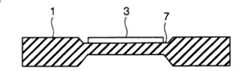
(示例3)使用如图1至5所示根据本发明的衬底热处理设备执行热处理。制造通过离子注入形成且具有如图7所示截面形状的p+n结二极管。(Example 3) Heat treatment was performed using the substrate heat treatment apparatus according to the present invention as shown in FIGS. 1 to 5 . A p+ n junction diode formed by ion implantation and having a cross-sectional shape as shown in FIG. 7 was fabricated.
5μm厚度的外延层通过在具有4°斜角的n+型4H-SiC(0001)衬底上牺牲氧化而形成,并且用氢氟酸进行处理。然后,使用离子注入装置,用30keV至170keV的注入能量以多阶段方式在500℃的注入温度下注入氮至350nm的深度以得到3×10²⁰/cm3的剂量。以这种方式得到的SiC衬底被用作衬底试样,并且使用根据本发明的衬底热处理设备(如图1至5中所示)而经受热处理。An epitaxial layer with a thickness of 5 μm was formed by sacrificial oxidation on an n+ type 4H-SiC (0001) substrate with a 4° off-angle, and treated with hydrofluoric acid. Then, using an ion implantation apparatus, nitrogen was implanted to a depth of 350 nm at an implantation temperature of 500° C. to obtain a dose of 3×10²⁰ /cm3 in a multi-stage manner with an implantation energy of 30 keV to 170 keV. The SiC substrate obtained in this way was used as a substrate sample, and subjected to heat treatment using a substrate heat treatment apparatus (as shown in FIGS. 1 to 5 ) according to the present invention.
衬底试样布置在衬底台架1上,使得离子注入表面面朝上(加热单元B的散热表面2侧)。在加热单元B的散热表面2与该衬底试样的氮离子注入表面之间的间隙设置成5mm。衬底试样通过在10-4Pa的减压气氛中加热1分钟而进行热处理。在加热期间散热表面2的温度设置成1,700℃、1,800℃和1,900℃。The substrate sample is arranged on the
为了评估热处理过的衬底试样的表面平坦度,用AFM阻尼模式在4μm×4μm的测量区域范围内测量在各上述温度下热处理之前和 热处理之后试样的RMS值。表2示出测量得到的RMS值。In order to evaluate the surface flatness of the heat-treated substrate samples, the RMS values of the samples before and after heat treatment at each of the above temperatures were measured in AFM damping mode within a measurement area of 4 μm × 4 μm. Table 2 shows the measured RMS values.
随后,每个热处理过的试样进行牺牲氧化且用氢氟酸清洁以去除表面变质层。然后,执行二氧化硅的图案化。通过使用CF4+Ar气混合物的RIE(反应离子刻蚀)装置,以100μm直径刻蚀SiC层至1μm深度,由此形成台面结构。Subsequently, each heat-treated sample was sacrificially oxidized and cleaned with hydrofluoric acid to remove the surface deterioration layer. Then, patterning of silicon dioxide is performed. The SiC layer was etched with a diameter of 100 μm to a depth of 1 μm by an RIE (Reactive Ion Etching) apparatus using a CF4 +Ar gas mixture, thereby forming a mesa structure.
随后,使用真空沉积装置,分别沉积20nm和100nm的钛(Ti)和铝(Al)。将所得到的试样在900℃下在氩(Ar)气气氛中进行热处理3分钟,由此形成欧姆电极。Subsequently, using a vacuum deposition apparatus, 20 nm and 100 nm of titanium (Ti) and aluminum (Al) were deposited, respectively. The obtained sample was heat-treated at 900° C. for 3 minutes in an argon (Ar) gas atmosphere, thereby forming an ohmic electrode.
为了评估得到的二极管的特性,在室温下使用“由Keithley制造的4200”测量电流密度-电压特性。In order to evaluate the characteristics of the obtained diode, current density-voltage characteristics were measured at room temperature using "4200 manufactured by Keithley".
(表2)
如表2中所示,每个衬底试样在热处理之后的表面平坦度展现出几乎等于RM nm的较小值,甚至在衬底试样在1,900℃温度下进行热处理1分钟之后。因此,衬底试样十分平坦。As shown in Table 2, the surface flatness of each substrate sample after heat treatment exhibited a small value almost equal to RM nm even after the substrate sample was heat-treated at a temperature of 1,900° C. for 1 minute. Therefore, the substrate sample is quite flat.
图8示出,当热处理温度是1,700℃、1,800℃和1,900℃时p+n二极管的电流密度-电压特性。FIG. 8 shows the current density-voltage characteristics of p+ n diodes when the heat treatment temperature is 1,700°C, 1,800°C, and 1,900°C.
当正向电压是0V至2V时,在1,700℃和1,800℃的热处理温度下测量到较大的漏电流密度。在反向电压区域中,在1,700℃和1,800℃的热处理温度下测量到10-4A量级上的较大的漏电流密度。When the forward voltage was 0 V to 2 V, larger leakage current densities were measured at the heat treatment temperatures of 1,700° C. and 1,800° C. In the reverse voltage region, large leakage current densities on the order of 10-4 A were measured at the heat treatment temperatures of 1,700°C and 1,800°C.
在1,900℃的热处理温度下,在反向电压区域中几乎测量不到漏电流密度。即使在正向电压区域中,也只是测量到非常小的10-6A量级上的漏电流密度。这可能是因为:通过离子注入在pn结界面中形成的晶体缺陷由于在1,900℃的热处理温度下的高温处理而消失了。At the heat treatment temperature of 1,900°C, the leakage current density was hardly measured in the reverse voltage region. Even in the forward voltage region, only very small leakage current densities on the order of 10−6 A were measured. This is probably because crystal defects formed in the pn junction interface by ion implantation disappeared due to high-temperature treatment at a heat treatment temperature of 1,900°C.
根据本发明的衬底热处理设备以这种方式能够制造非常好的p+n结二极管。这种pn结不但用在pn结二极管,而且也用在场效应晶体管(MOS-FET)、结型晶体管(J-FET)、MES-FET、以及双极晶体管(BJT)中。这样提高了使用这种SiC的电子器件的特 性,导致生产力的较大提高。The substrate heat treatment device according to the invention enables the production of very good p+ n junction diodes in this way. This pn junction is used not only in pn junction diodes, but also in field effect transistors (MOS-FETs), junction transistors (J-FETs), MES-FETs, and bipolar transistors (BJTs). This improves the characteristics of electronic devices using this SiC, resulting in a large improvement in productivity.
这样,根据本发明,衬底可以有效地在短时间段内均匀地加热至高温,并且在短时间段内冷却。衬底由此可以在不损害机械手的情况下被传输。甚至在接近2,000℃的超高温下也可以实现实用的吞吐量。Thus, according to the present invention, the substrate can be efficiently uniformly heated to a high temperature in a short period of time, and cooled in a short period of time. The substrate can thus be transported without damaging the robot. Practical throughput can be achieved even at ultra-high temperatures approaching 2,000°C.
已经参照附图说明本发明的优选实施例。应注意,本发明不限于上述实施例并且在从权利要求所得到的技术范围内可以以多种方式进行改变。Preferred embodiments of the present invention have been described with reference to the accompanying drawings. It should be noted that the present invention is not limited to the above-described embodiments and can be changed in various ways within the technical scope obtained from the claims.
本发明不限于上述实施例,并且在不脱离本发明的精神和范围的前提下可以进行多种改变和修改。因此,为了告知公众本发明的范围,附上以下权利要求。The present invention is not limited to the above-described embodiments, and various changes and modifications can be made without departing from the spirit and scope of the present invention. Therefore, to apprise the public of the scope of the present invention, the following claims are appended.
该申请基于且要求2007年9月3号提交的在先日本专利申请No.2007-227449(其全部内容通过参考包含于此)的优先权。 This application is based on and claims priority from prior Japanese Patent Application No. 2007-227449 filed on September 3, 2007, the entire contents of which are hereby incorporated by reference. the
Claims (14)
Translated fromChineseApplications Claiming Priority (3)
| Application Number | Priority Date | Filing Date | Title |
|---|---|---|---|
| JP227449/2007 | 2007-09-03 | ||
| JP2007227449 | 2007-09-03 | ||
| PCT/JP2008/065395WO2009031450A1 (en) | 2007-09-03 | 2008-08-28 | Substrate heat-treating apparatus, and substrate heat-treating method |
Publications (2)
| Publication Number | Publication Date |
|---|---|
| CN101569000A CN101569000A (en) | 2009-10-28 |
| CN101569000Btrue CN101569000B (en) | 2011-07-13 |
Family
ID=40428771
Family Applications (1)
| Application Number | Title | Priority Date | Filing Date |
|---|---|---|---|
| CN2008800011475AActiveCN101569000B (en) | 2007-09-03 | 2008-08-28 | Substrate heat-treating apparatus, and substrate heat-treating method |
Country Status (4)
| Country | Link |
|---|---|
| US (1) | US8090245B2 (en) |
| JP (2) | JP4288309B2 (en) |
| CN (1) | CN101569000B (en) |
| WO (1) | WO2009031450A1 (en) |
Families Citing this family (35)
| Publication number | Priority date | Publication date | Assignee | Title |
|---|---|---|---|---|
| WO2008123111A1 (en)* | 2007-03-20 | 2008-10-16 | Canon Anelva Corporation | Substrate heat treatment device and substrate heat treatment method |
| JP4436893B2 (en)* | 2007-05-16 | 2010-03-24 | キヤノンアネルバ株式会社 | Heat treatment device |
| JP4601701B2 (en)* | 2008-11-13 | 2010-12-22 | シャープ株式会社 | Vapor phase growth apparatus and gas supply method |
| USD640715S1 (en)* | 2008-11-17 | 2011-06-28 | Applied Materials, Inc. | Lift pin assembly |
| USD635597S1 (en)* | 2008-11-17 | 2011-04-05 | Applied Materials, Inc. | Lift pin |
| JP5620090B2 (en) | 2008-12-15 | 2014-11-05 | キヤノンアネルバ株式会社 | Substrate processing apparatus, heat-treated substrate manufacturing method, and semiconductor device manufacturing method |
| USD650818S1 (en)* | 2008-12-19 | 2011-12-20 | Applied Materials, Inc. | Inner lift pin |
| JP2010251718A (en)* | 2009-03-27 | 2010-11-04 | Canon Anelva Corp | Temperature control method for heating device and storage medium |
| SG176270A1 (en) | 2009-05-29 | 2012-01-30 | Jx Nippon Oil & Energy Corp | Isobutylene-based polymer and method for producing same |
| WO2011016223A1 (en)* | 2009-08-04 | 2011-02-10 | キヤノンアネルバ株式会社 | Heat treatment apparatus and method for manufacturing semiconductor device |
| US9431281B2 (en) | 2009-12-25 | 2016-08-30 | Canon Anelva Corporation | Temperature control method for substrate heat treatment apparatus, semiconductor device manufacturing method, temperature control program for substrate heat treatment apparatus, and recording medium |
| US8367531B1 (en) | 2010-03-23 | 2013-02-05 | L'air Liquide Societe Anonyme Pour L'etude Et L'exploitation Des Procedes Georges Claude | Aluminum implant using new compounds |
| JP5517766B2 (en)* | 2010-06-16 | 2014-06-11 | キヤノン株式会社 | Exposure apparatus and device manufacturing method |
| US9719169B2 (en)* | 2010-12-20 | 2017-08-01 | Novellus Systems, Inc. | System and apparatus for flowable deposition in semiconductor fabrication |
| JP5697441B2 (en)* | 2010-12-28 | 2015-04-08 | キヤノンアネルバ株式会社 | Substrate heat treatment equipment |
| US20120196242A1 (en)* | 2011-01-27 | 2012-08-02 | Applied Materials, Inc. | Substrate support with heater and rapid temperature change |
| US20130067761A1 (en)* | 2011-09-16 | 2013-03-21 | Shenzhen China Star Optoelectronics Technology Co. Ltd. | Drying apparatus |
| TWI534341B (en)* | 2011-09-26 | 2016-05-21 | Hitachi Int Electric Inc | A substrate processing apparatus, a manufacturing method of a semiconductor device, and a recording medium |
| US10224182B2 (en) | 2011-10-17 | 2019-03-05 | Novellus Systems, Inc. | Mechanical suppression of parasitic plasma in substrate processing chamber |
| CN104040691B (en)* | 2011-12-27 | 2016-09-07 | 佳能安内华股份有限公司 | Substrate heat treatment device |
| JP6311955B2 (en)* | 2012-07-24 | 2018-04-18 | 日立金属株式会社 | Mold quenching method |
| JP2014110294A (en)* | 2012-11-30 | 2014-06-12 | Panasonic Corp | Vacuum heating furnace and manufacturing method of organic semiconductor element |
| JP2014194921A (en)* | 2013-03-01 | 2014-10-09 | Tokyo Electron Ltd | Microwave processor and microwave processing method |
| US9165773B2 (en) | 2013-05-28 | 2015-10-20 | Praxair Technology, Inc. | Aluminum dopant compositions, delivery package and method of use |
| US9847222B2 (en) | 2013-10-25 | 2017-12-19 | Lam Research Corporation | Treatment for flowable dielectric deposition on substrate surfaces |
| JP6245475B2 (en)* | 2014-07-30 | 2017-12-13 | 公益財団法人鉄道総合技術研究所 | Manufacturing method of dissimilar metal composite member |
| US10049921B2 (en) | 2014-08-20 | 2018-08-14 | Lam Research Corporation | Method for selectively sealing ultra low-k porous dielectric layer using flowable dielectric film formed from vapor phase dielectric precursor |
| US10388546B2 (en) | 2015-11-16 | 2019-08-20 | Lam Research Corporation | Apparatus for UV flowable dielectric |
| JP6697089B2 (en)* | 2016-03-18 | 2020-05-20 | エーシーエム リサーチ (シャンハイ) インコーポレーテッド | Substrate heat treatment equipment |
| IT201600099783A1 (en)* | 2016-10-05 | 2018-04-05 | Lpe Spa | REACTOR FOR EPITAXIAL DEPOSITION WITH EXTERIOR REFLECTOR OF THE REACTION CHAMBER AND METHOD OF COOLING A SUSCECTOR AND SUBSTRATES |
| US10861731B2 (en)* | 2017-01-19 | 2020-12-08 | Axcelis Technologies, Inc. | Radiant heating presoak |
| KR102242975B1 (en)* | 2017-03-09 | 2021-04-23 | 주식회사 원익아이피에스 | Substrate processing apparatus |
| CN108060406B (en)* | 2018-01-29 | 2023-09-08 | 北京北方华创微电子装备有限公司 | Shielding platen assembly, semiconductor processing apparatus and method |
| CN109888129B (en)* | 2019-01-30 | 2020-12-08 | 武汉华星光电半导体显示技术有限公司 | Apparatus and method for removing bubbles in flexible substrate |
| JP2021197448A (en)* | 2020-06-15 | 2021-12-27 | 光洋サーモシステム株式会社 | Thermal treatment device |
Citations (2)
| Publication number | Priority date | Publication date | Assignee | Title |
|---|---|---|---|---|
| US6497767B1 (en)* | 1999-05-14 | 2002-12-24 | Tokyo Electron Limited | Thermal processing unit for single substrate |
| CN1667803A (en)* | 2005-04-01 | 2005-09-14 | 河北工业大学 | Silicon carbide heat treatment apparatus and method |
Family Cites Families (24)
| Publication number | Priority date | Publication date | Assignee | Title |
|---|---|---|---|---|
| US5429498A (en)* | 1991-12-13 | 1995-07-04 | Tokyo Electron Sagami Kabushiki Kaisha | Heat treatment method and apparatus thereof |
| US5662469A (en)* | 1991-12-13 | 1997-09-02 | Tokyo Electron Tohoku Kabushiki Kaisha | Heat treatment method |
| JP3507548B2 (en)* | 1994-03-31 | 2004-03-15 | 東京エレクトロン株式会社 | Heat treatment method |
| JP3210051B2 (en)* | 1992-01-16 | 2001-09-17 | 株式会社東芝 | Vapor phase growth equipment |
| US5444217A (en)* | 1993-01-21 | 1995-08-22 | Moore Epitaxial Inc. | Rapid thermal processing apparatus for processing semiconductor wafers |
| JP3711291B2 (en)* | 1993-06-18 | 2005-11-02 | 東京エレクトロン株式会社 | Heat treatment equipment |
| JP3382064B2 (en)* | 1995-06-29 | 2003-03-04 | 株式会社東芝 | Heat treatment equipment |
| JPH1045474A (en) | 1996-08-01 | 1998-02-17 | Toyo Tanso Kk | Production of graphite material coated with pyrolyzed carbon |
| JP3067658B2 (en)* | 1996-10-17 | 2000-07-17 | イートン コーポレーション | Wafer heat treatment equipment |
| US6027244A (en)* | 1997-07-24 | 2000-02-22 | Steag Rtp Systems, Inc. | Apparatus for determining the temperature of a semi-transparent radiating body |
| US6156079A (en)* | 1998-10-21 | 2000-12-05 | Ho; Henry | Window support member for a semiconductor processing system |
| US6091889A (en)* | 1999-01-08 | 2000-07-18 | National Science Council | Rapid thermal processor for heating a substrate |
| US6087632A (en)* | 1999-01-11 | 2000-07-11 | Tokyo Electron Limited | Heat processing device with hot plate and associated reflector |
| US6313443B1 (en)* | 1999-04-20 | 2001-11-06 | Steag Cvd Systems, Ltd. | Apparatus for processing material at controlled temperatures |
| US7075037B2 (en)* | 2001-03-02 | 2006-07-11 | Tokyo Electron Limited | Heat treatment apparatus using a lamp for rapidly and uniformly heating a wafer |
| JP2003318076A (en) | 2002-04-23 | 2003-11-07 | Canon Inc | Method and apparatus for heating and cooling substrate in vacuum |
| CN1303647C (en)* | 2003-09-30 | 2007-03-07 | 佳能株式会社 | Heating method, heating apparatus, and production method of image display apparatus |
| JP2005299990A (en) | 2004-04-09 | 2005-10-27 | Daiichi Kiden:Kk | High temperature heating device |
| JP2005302936A (en)* | 2004-04-09 | 2005-10-27 | Sumitomo Osaka Cement Co Ltd | Plasma processing apparatus |
| JP2008166729A (en)* | 2006-12-08 | 2008-07-17 | Canon Anelva Corp | Substrate heating apparatus and semiconductor manufacturing method |
| WO2008123111A1 (en)* | 2007-03-20 | 2008-10-16 | Canon Anelva Corporation | Substrate heat treatment device and substrate heat treatment method |
| JP5468784B2 (en)* | 2008-01-30 | 2014-04-09 | キヤノンアネルバ株式会社 | Substrate heating apparatus, heat treatment method, and method for manufacturing semiconductor device |
| JP4520512B2 (en)* | 2008-02-13 | 2010-08-04 | キヤノンアネルバ株式会社 | Heating device |
| JP4617364B2 (en)* | 2008-02-29 | 2011-01-26 | キヤノンアネルバ株式会社 | Substrate heating apparatus and processing method |
- 2008
- 2008-08-28JPJP2008555546Apatent/JP4288309B2/enactiveActive
- 2008-08-28CNCN2008800011475Apatent/CN101569000B/enactiveActive
- 2008-08-28WOPCT/JP2008/065395patent/WO2009031450A1/ennot_activeCeased
- 2009
- 2009-03-30JPJP2009081684Apatent/JP4988785B2/enactiveActive
- 2009-04-03USUS12/418,063patent/US8090245B2/enactiveActive
Patent Citations (2)
| Publication number | Priority date | Publication date | Assignee | Title |
|---|---|---|---|---|
| US6497767B1 (en)* | 1999-05-14 | 2002-12-24 | Tokyo Electron Limited | Thermal processing unit for single substrate |
| CN1667803A (en)* | 2005-04-01 | 2005-09-14 | 河北工业大学 | Silicon carbide heat treatment apparatus and method |
Non-Patent Citations (1)
| Title |
|---|
| JP特开平10-125690A 1998.05.15 |
Also Published As
| Publication number | Publication date |
|---|---|
| US8090245B2 (en) | 2012-01-03 |
| JPWO2009031450A1 (en) | 2010-12-16 |
| JP2009147392A (en) | 2009-07-02 |
| US20090190908A1 (en) | 2009-07-30 |
| WO2009031450A1 (en) | 2009-03-12 |
| JP4288309B2 (en) | 2009-07-01 |
| CN101569000A (en) | 2009-10-28 |
| JP4988785B2 (en) | 2012-08-01 |
Similar Documents
| Publication | Publication Date | Title |
|---|---|---|
| CN101569000B (en) | Substrate heat-treating apparatus, and substrate heat-treating method | |
| US20100226630A1 (en) | Apparatus for heat-treating substrate and substrate manufacturing method | |
| JP5620090B2 (en) | Substrate processing apparatus, heat-treated substrate manufacturing method, and semiconductor device manufacturing method | |
| US9603195B2 (en) | Substrate heat treatment apparatus | |
| JP4409756B2 (en) | Dual substrate load-lock process equipment | |
| JP5214774B2 (en) | Substrate processing apparatus and semiconductor device manufacturing method | |
| KR200496202Y1 (en) | Methods and apparatus for processing a substrate | |
| JP6588423B2 (en) | Semiconductor substrate heat treatment method, semiconductor substrate manufacturing method, heat treatment apparatus, and substrate processing system | |
| US10425990B2 (en) | Vacuum processing device | |
| TW201320221A (en) | Substrate cooling device, substrate cooling method and heat treatment apparatus | |
| CN102473641B (en) | Heat treatment equipment and semiconductor device manufacturing method | |
| JP5478041B2 (en) | Annealing equipment, heat treatment method | |
| JP2005019725A (en) | Annealing device and annealing method | |
| JP2006093543A (en) | Thermal processing apparatus | |
| JP2008283143A (en) | Treatment equipment, and transistor manufacturing method | |
| JP2002093715A (en) | Semiconductor manufacturing equipment | |
| WO2005017988A1 (en) | Substrate processing apparatus and method for manufacturing semiconductor device | |
| JPH10223722A (en) | Semiconductor processing equipment | |
| JP2002289669A (en) | Substrate processing equipment |
Legal Events
| Date | Code | Title | Description |
|---|---|---|---|
| C06 | Publication | ||
| PB01 | Publication | ||
| C10 | Entry into substantive examination | ||
| SE01 | Entry into force of request for substantive examination | ||
| C14 | Grant of patent or utility model | ||
| GR01 | Patent grant |