CN101557904A - CMP pad conditioner and associated methods - Google Patents
CMP pad conditioner and associated methodsDownload PDFInfo
- Publication number
- CN101557904A CN101557904ACNA2007800463355ACN200780046335ACN101557904ACN 101557904 ACN101557904 ACN 101557904ACN A2007800463355 ACNA2007800463355 ACN A2007800463355ACN 200780046335 ACN200780046335 ACN 200780046335ACN 101557904 ACN101557904 ACN 101557904A
- Authority
- CN
- China
- Prior art keywords
- cutting
- polishing pad
- cutting element
- cmp
- pad
- Prior art date
- Legal status (The legal status is an assumption and is not a legal conclusion. Google has not performed a legal analysis and makes no representation as to the accuracy of the status listed.)
- Pending
Links
- 238000000034methodMethods0.000titleclaimsabstractdescription44
- 238000005520cutting processMethods0.000claimsabstractdescription243
- 238000005498polishingMethods0.000claimsabstractdescription154
- 239000000463materialSubstances0.000claimsabstractdescription79
- 230000006835compressionEffects0.000claimsabstractdescription9
- 238000007906compressionMethods0.000claimsabstractdescription9
- 239000010432diamondSubstances0.000claimsdescription26
- 229910003460diamondInorganic materials0.000claimsdescription23
- 239000000126substanceSubstances0.000claimsdescription8
- 229910052582BNInorganic materials0.000claimsdescription7
- PZNSFCLAULLKQX-UHFFFAOYSA-NBoron nitrideChemical compoundN#BPZNSFCLAULLKQX-UHFFFAOYSA-N0.000claimsdescription7
- 239000010410layerSubstances0.000description27
- 239000000758substrateSubstances0.000description25
- 235000012431wafersNutrition0.000description25
- XUIMIQQOPSSXEZ-UHFFFAOYSA-NSiliconChemical compound[Si]XUIMIQQOPSSXEZ-UHFFFAOYSA-N0.000description21
- 239000010703siliconSubstances0.000description21
- 229910052710siliconInorganic materials0.000description21
- 229920005989resinPolymers0.000description20
- 239000011347resinSubstances0.000description20
- 230000003750conditioning effectEffects0.000description10
- 239000002245particleSubstances0.000description10
- 239000000203mixtureSubstances0.000description9
- MCMNRKCIXSYSNV-UHFFFAOYSA-NZirconium dioxideChemical compoundO=[Zr]=OMCMNRKCIXSYSNV-UHFFFAOYSA-N0.000description8
- 230000001143conditioned effectEffects0.000description8
- 229920002037poly(vinyl butyral) polymerPolymers0.000description8
- 125000006850spacer groupChemical group0.000description8
- 239000003082abrasive agentSubstances0.000description7
- 239000000853adhesiveSubstances0.000description7
- 230000001070adhesive effectEffects0.000description7
- 238000004519manufacturing processMethods0.000description7
- 238000005229chemical vapour depositionMethods0.000description6
- 229910052751metalInorganic materials0.000description6
- 239000002184metalSubstances0.000description6
- UONOETXJSWQNOL-UHFFFAOYSA-Ntungsten carbideChemical compound[W+]#[C-]UONOETXJSWQNOL-UHFFFAOYSA-N0.000description6
- 229910052581Si3N4Inorganic materials0.000description5
- 239000000919ceramicSubstances0.000description5
- 239000011368organic materialSubstances0.000description5
- HQVNEWCFYHHQES-UHFFFAOYSA-Nsilicon nitrideChemical compoundN12[Si]34N5[Si]62N3[Si]51N64HQVNEWCFYHHQES-UHFFFAOYSA-N0.000description5
- 239000007787solidSubstances0.000description5
- OKTJSMMVPCPJKN-UHFFFAOYSA-NCarbonChemical compound[C]OKTJSMMVPCPJKN-UHFFFAOYSA-N0.000description4
- 239000004372Polyvinyl alcoholSubstances0.000description4
- 238000000227grindingMethods0.000description4
- 239000007788liquidSubstances0.000description4
- VNWKTOKETHGBQD-UHFFFAOYSA-NmethaneChemical compoundCVNWKTOKETHGBQD-UHFFFAOYSA-N0.000description4
- 239000012188paraffin waxSubstances0.000description4
- 229920003023plasticPolymers0.000description4
- 239000004033plasticSubstances0.000description4
- 229920002451polyvinyl alcoholPolymers0.000description4
- 230000008569processEffects0.000description4
- HBMJWWWQQXIZIP-UHFFFAOYSA-Nsilicon carbideChemical compound[Si+]#[C-]HBMJWWWQQXIZIP-UHFFFAOYSA-N0.000description4
- 230000003746surface roughnessEffects0.000description4
- RYGMFSIKBFXOCR-UHFFFAOYSA-NCopperChemical compound[Cu]RYGMFSIKBFXOCR-UHFFFAOYSA-N0.000description3
- LYCAIKOWRPUZTN-UHFFFAOYSA-NEthylene glycolChemical compoundOCCOLYCAIKOWRPUZTN-UHFFFAOYSA-N0.000description3
- VYPSYNLAJGMNEJ-UHFFFAOYSA-NSilicium dioxideChemical compoundO=[Si]=OVYPSYNLAJGMNEJ-UHFFFAOYSA-N0.000description3
- 229910052802copperInorganic materials0.000description3
- 239000010949copperSubstances0.000description3
- 239000012530fluidSubstances0.000description3
- 239000011521glassSubstances0.000description3
- 150000002739metalsChemical class0.000description3
- 239000000843powderSubstances0.000description3
- 229910010271silicon carbideInorganic materials0.000description3
- KXGFMDJXCMQABM-UHFFFAOYSA-N2-methoxy-6-methylphenolChemical compound[CH]OC1=CC=CC([CH])=C1OKXGFMDJXCMQABM-UHFFFAOYSA-N0.000description2
- 239000004925Acrylic resinSubstances0.000description2
- 229920000178Acrylic resinPolymers0.000description2
- 239000004593EpoxySubstances0.000description2
- 239000002202Polyethylene glycolSubstances0.000description2
- 239000011230binding agentSubstances0.000description2
- 229910052799carbonInorganic materials0.000description2
- 239000010941cobaltSubstances0.000description2
- 229910017052cobaltInorganic materials0.000description2
- GUTLYIVDDKVIGB-UHFFFAOYSA-Ncobalt atomChemical compound[Co]GUTLYIVDDKVIGB-UHFFFAOYSA-N0.000description2
- 239000002131composite materialSubstances0.000description2
- 238000000151depositionMethods0.000description2
- 230000008021depositionEffects0.000description2
- 238000009826distributionMethods0.000description2
- 230000000694effectsEffects0.000description2
- 238000009760electrical discharge machiningMethods0.000description2
- 239000000839emulsionSubstances0.000description2
- 239000010408filmSubstances0.000description2
- 229910052739hydrogenInorganic materials0.000description2
- 239000001257hydrogenSubstances0.000description2
- 150000002894organic compoundsChemical class0.000description2
- 229920001568phenolic resinPolymers0.000description2
- 239000005011phenolic resinSubstances0.000description2
- 229920001223polyethylene glycolPolymers0.000description2
- 229920000642polymerPolymers0.000description2
- 229920002635polyurethanePolymers0.000description2
- 239000004814polyurethaneSubstances0.000description2
- 239000002243precursorSubstances0.000description2
- 238000007790scrapingMethods0.000description2
- 239000002002slurrySubstances0.000description2
- 239000010935stainless steelSubstances0.000description2
- 229910001220stainless steelInorganic materials0.000description2
- 238000009966trimmingMethods0.000description2
- UFHFLCQGNIYNRP-UHFFFAOYSA-NHydrogenChemical compound[H][H]UFHFLCQGNIYNRP-UHFFFAOYSA-N0.000description1
- YZCKVEUIGOORGS-UHFFFAOYSA-NHydrogen atomChemical compound[H]YZCKVEUIGOORGS-UHFFFAOYSA-N0.000description1
- MHAJPDPJQMAIIY-UHFFFAOYSA-NHydrogen peroxideChemical compoundOOMHAJPDPJQMAIIY-UHFFFAOYSA-N0.000description1
- RTAQQCXQSZGOHL-UHFFFAOYSA-NTitaniumChemical compound[Ti]RTAQQCXQSZGOHL-UHFFFAOYSA-N0.000description1
- 229910026551ZrCInorganic materials0.000description1
- OTCHGXYCWNXDOA-UHFFFAOYSA-N[C].[Zr]Chemical compound[C].[Zr]OTCHGXYCWNXDOA-UHFFFAOYSA-N0.000description1
- 238000005299abrasionMethods0.000description1
- NIXOWILDQLNWCW-UHFFFAOYSA-Nacrylic acid groupChemical groupC(C=C)(=O)ONIXOWILDQLNWCW-UHFFFAOYSA-N0.000description1
- 230000009471actionEffects0.000description1
- 239000000956alloySubstances0.000description1
- CAVCGVPGBKGDTG-UHFFFAOYSA-Nalumanylidynemethyl(alumanylidynemethylalumanylidenemethylidene)alumaneChemical compound[Al]#C[Al]=C=[Al]C#[Al]CAVCGVPGBKGDTG-UHFFFAOYSA-N0.000description1
- 229910052782aluminiumInorganic materials0.000description1
- XAGFODPZIPBFFR-UHFFFAOYSA-NaluminiumChemical compound[Al]XAGFODPZIPBFFR-UHFFFAOYSA-N0.000description1
- PNEYBMLMFCGWSK-UHFFFAOYSA-Naluminium oxideInorganic materials[O-2].[O-2].[O-2].[Al+3].[Al+3]PNEYBMLMFCGWSK-UHFFFAOYSA-N0.000description1
- 125000004429atomChemical group0.000description1
- 230000004888barrier functionEffects0.000description1
- 238000005219brazingMethods0.000description1
- 239000000872bufferSubstances0.000description1
- 238000005266castingMethods0.000description1
- 230000003197catalytic effectEffects0.000description1
- 238000006243chemical reactionMethods0.000description1
- 238000005352clarificationMethods0.000description1
- 239000004927claySubstances0.000description1
- 239000011248coating agentSubstances0.000description1
- 238000000576coating methodMethods0.000description1
- 239000012141concentrateSubstances0.000description1
- 239000000470constituentSubstances0.000description1
- 238000007796conventional methodMethods0.000description1
- 238000001816coolingMethods0.000description1
- 229920001577copolymerPolymers0.000description1
- 239000010431corundumSubstances0.000description1
- 229910052593corundumInorganic materials0.000description1
- 230000001419dependent effectEffects0.000description1
- 230000000881depressing effectEffects0.000description1
- 230000003001depressive effectEffects0.000description1
- 238000010586diagramMethods0.000description1
- 229920001971elastomerPolymers0.000description1
- 238000005516engineering processMethods0.000description1
- 239000003822epoxy resinSubstances0.000description1
- 239000012634fragmentSubstances0.000description1
- 238000013467fragmentationMethods0.000description1
- 238000006062fragmentation reactionMethods0.000description1
- 239000003292glueSubstances0.000description1
- 239000010439graphiteSubstances0.000description1
- 229910002804graphiteInorganic materials0.000description1
- -1gravelSubstances0.000description1
- 238000009499grossingMethods0.000description1
- 150000002431hydrogenChemical class0.000description1
- 230000008595infiltrationEffects0.000description1
- 238000001764infiltrationMethods0.000description1
- 239000011159matrix materialSubstances0.000description1
- 229910001092metal group alloyInorganic materials0.000description1
- 238000012986modificationMethods0.000description1
- 230000004048modificationEffects0.000description1
- 239000000178monomerSubstances0.000description1
- 230000006911nucleationEffects0.000description1
- 238000010899nucleationMethods0.000description1
- 239000004482other powderSubstances0.000description1
- 239000007800oxidant agentSubstances0.000description1
- 230000035515penetrationEffects0.000description1
- 229920000647polyepoxidePolymers0.000description1
- 238000006116polymerization reactionMethods0.000description1
- 238000003825pressingMethods0.000description1
- 230000001737promoting effectEffects0.000description1
- 239000010453quartzSubstances0.000description1
- 238000004064recyclingMethods0.000description1
- 230000009467reductionEffects0.000description1
- 230000008439repair processEffects0.000description1
- 230000004044responseEffects0.000description1
- 238000007788rougheningMethods0.000description1
- 239000005060rubberSubstances0.000description1
- 238000005488sandblastingMethods0.000description1
- 229910052594sapphireInorganic materials0.000description1
- 239000010980sapphireSubstances0.000description1
- 238000006748scratchingMethods0.000description1
- 230000002393scratching effectEffects0.000description1
- 239000004065semiconductorSubstances0.000description1
- 238000000926separation methodMethods0.000description1
- 239000000377silicon dioxideSubstances0.000description1
- 238000005245sinteringMethods0.000description1
- 239000007779soft materialSubstances0.000description1
- 239000011343solid materialSubstances0.000description1
- 239000002904solventSubstances0.000description1
- 239000007921spraySubstances0.000description1
- 239000010421standard materialSubstances0.000description1
- 239000002344surface layerSubstances0.000description1
- 239000000725suspensionSubstances0.000description1
- MZLGASXMSKOWSE-UHFFFAOYSA-Ntantalum nitrideChemical compound[Ta]#NMZLGASXMSKOWSE-UHFFFAOYSA-N0.000description1
- 239000010936titaniumSubstances0.000description1
- 229910052719titaniumInorganic materials0.000description1
- 239000002966varnishSubstances0.000description1
- XLYOFNOQVPJJNP-UHFFFAOYSA-NwaterSubstancesOXLYOFNOQVPJJNP-UHFFFAOYSA-N0.000description1
- 239000001993waxSubstances0.000description1
- 238000003466weldingMethods0.000description1
Images


Classifications
- B—PERFORMING OPERATIONS; TRANSPORTING
- B24—GRINDING; POLISHING
- B24B—MACHINES, DEVICES, OR PROCESSES FOR GRINDING OR POLISHING; DRESSING OR CONDITIONING OF ABRADING SURFACES; FEEDING OF GRINDING, POLISHING, OR LAPPING AGENTS
- B24B53/00—Devices or means for dressing or conditioning abrasive surfaces
- B24B53/017—Devices or means for dressing, cleaning or otherwise conditioning lapping tools
Landscapes
- Engineering & Computer Science (AREA)
- Mechanical Engineering (AREA)
- Mechanical Treatment Of Semiconductor (AREA)
- Finish Polishing, Edge Sharpening, And Grinding By Specific Grinding Devices (AREA)
- Grinding-Machine Dressing And Accessory Apparatuses (AREA)
- Polishing Bodies And Polishing Tools (AREA)
Abstract
Translated fromChineseDescription
Translated fromChinese技术领域technical field
本发明主要是关于一种用于从化学机械抛光垫(CMP)上移除(如磨平(smooth)、抛光(polish)、修整(dress)等)材料的工具和方法。因此,本发明涵盖化学、物理以及材料科学领域。The present invention generally relates to a tool and method for removing (eg, smoothing, polishing, dressing, etc.) material from a chemical mechanical polishing pad (CMP). Accordingly, the present invention encompasses the fields of chemistry, physics and materials science.
背景技术Background technique
抛光材料广泛应用于抛光、刨平(planing)、修整或调整等加工处理,例如,半导体产业目前每年花费超过十亿美元制造硅晶圆,其必须表现出非常平坦且平滑的表面。已知用于制造平滑且平坦表面的硅晶圆的技术为数众多,其中最常见的技术就是化学机械抛光(CMP)法,其包括以抛光垫结合研磨液使用,这些CMP垫的修整可利用多种工具完成。Polishing materials are widely used in processing such as polishing, planing, trimming or conditioning. For example, the semiconductor industry currently spends more than one billion dollars a year to manufacture silicon wafers, which must exhibit a very flat and smooth surface. Numerous techniques are known for making silicon wafers with smooth and planar surfaces, the most common of which is chemical mechanical polishing (CMP), which involves the use of polishing pads in combination with abrasive slurries. The tool is completed.
发明内容Contents of the invention
有关于一实施例,本发明提供一种在调整化学机械研磨抛光垫(CMP抛光垫)时减少该CMP抛光垫的压缩程度的方法,其包括:结合该CMP抛光垫与至少一超硬切割元件,该超硬切割元件包括一切割面,该切割面相对于该CMP抛光垫的磨光表面具有等于或小于90度的角度;以及将CMP抛光垫相对于该切割元件的方向移动,令该切割面将材料从该CMP抛光垫移除,以调整该CMP抛光垫。In relation to one embodiment, the present invention provides a method of reducing the degree of compression of a chemical mechanical polishing pad (CMP pad) when conditioning the pad, comprising: combining the CMP pad with at least one superhard cutting element , the superhard cutting element includes a cutting surface having an angle equal to or less than 90 degrees with respect to the polishing surface of the CMP polishing pad; and moving the CMP polishing pad in a direction relative to the cutting element such that the cutting surface Material is removed from the CMP polishing pad to condition the CMP polishing pad.
关于另一态样,本发明提供一种使CMP抛光垫的压缩最小化且从该CMP抛光垫移除材料的抛光垫调整器,其包括:一基座以及复数切割元件,其是从该基座延伸出来,各切割元件相对于该CMP抛光垫的磨光表面具有等于或小于90度的角度;该切割元件的面被定向,使得该抛光垫调整器和CMP抛光垫的相对移动,令从CMP抛光垫以该切割面移除材料,而调整该CMP抛光垫。In yet another aspect, the present invention provides a polishing pad conditioner for minimizing compression of a CMP polishing pad and removing material from the CMP polishing pad, comprising: a base and a plurality of cutting elements formed from the base Seats extend out, and each cutting element has an angle equal to or less than 90 degrees relative to the polishing surface of the CMP polishing pad; The CMP polishing pad adjusts the CMP polishing pad by removing material with the cut surface.
关于本发明的另一态样,一种在调整CMP抛光垫时减少该CMP抛光垫的压缩程度的方法,其包括:结合该CMP抛光垫与复数个由多晶钻石片所形成的超硬切割元件,各切割元件包括一切割面,该切割面相对于该CMP抛光垫的磨光表面具有等于或小于90度的角度;以及将CMP抛光垫相对于该切割元件的方向移动,令该切割面将材料从该CMP抛光垫移除,以调整该CMP抛光垫。Regarding another aspect of the present invention, a method for reducing the degree of compression of the CMP polishing pad when adjusting the CMP polishing pad includes: combining the CMP polishing pad with a plurality of superhard cutting pads formed by polycrystalline diamond chips elements, each cutting element comprising a cutting surface having an angle equal to or less than 90 degrees relative to the polishing surface of the CMP polishing pad; and moving the CMP polishing pad in a direction relative to the cutting element such that the cutting surface will Material is removed from the CMP polishing pad to condition the CMP polishing pad.
因此,上述已列出本发明各种重要的特色,因此在接下来的详细说明中可更进一步地理解,并且在本领域所做的贡献可能会有更佳的领会,而本发明的其他特征将会从接下来的详细说明及其附图和申请专利范围中变得更为清晰,也可能在实行本发明时得知。Therefore, the above-mentioned various important features of the present invention have been listed, so they can be further understood in the following detailed description, and the contributions made in this field may be better appreciated, while other features of the present invention It will become clearer from the following detailed description and its accompanying drawings and patent claims, and may also be learned during the practice of the present invention.
附图说明Description of drawings
图1是关于本发明一实施例的抛光垫调整器的立体图;1 is a perspective view of a polishing pad conditioner according to an embodiment of the present invention;
图2是关于本发明一实施例的抛光垫调整器的俯视图;2 is a top view of a polishing pad conditioner according to an embodiment of the present invention;
图3A是关于以既有方法调整的抛光垫的部份视图;FIG. 3A is a partial view of a polishing pad conditioned by a conventional method;
图3B是关于以本发明一实施例调整的抛光垫的部份视图;Figure 3B is a partial view of a polishing pad conditioned according to one embodiment of the present invention;
图3C是关于以本发明另一实施例调整的抛光垫的部份视图;Figure 3C is a partial view of a polishing pad conditioned according to another embodiment of the present invention;
图3D涉及本发明另一实施例调整的抛光垫的部份视图;Figure 3D is a partial view of a conditioned polishing pad according to another embodiment of the present invention;
图4是包含具各种几何形状的切割元件的部份抛光垫调整器的立体图;4 is a perspective view of a portion of a polishing pad conditioner including cutting elements having various geometries;
图5是关于本发明一实施例的抛光垫调整器的侧面剖视图;5 is a side sectional view of a polishing pad conditioner according to an embodiment of the present invention;
图6A是关于本发明一实施例的抛光垫调整器的俯视图;Figure 6A is a top view of a polishing pad conditioner according to an embodiment of the present invention;
图6B是图6A的抛光垫调整器的剖视图;6B is a cross-sectional view of the polishing pad conditioner of FIG. 6A;
图7是关于本发明一实施例的部份抛光垫调整器的显微照片。Figure 7 is a photomicrograph of a portion of a pad conditioner according to one embodiment of the present invention.
附图标记说明:12-抛光垫调整器;14、14d-基座;16、16a~j-切割元件;18、18a~c-切割面;21-一般平面;22-方向;24、24a、24c-延伸边缘;26、26c-切割边缘。Explanation of reference signs: 12-polishing pad adjuster; 14, 14d-base; 16, 16a~j-cutting elements; 18, 18a~c-cutting surface; 21-general plane; 22-direction; 24, 24a, 24c - extending edge; 26, 26c - cutting edge.
具体实施方式Detailed ways
需要了解的是所附图式仅是进一步了解本发明而作为描述用途,该图式并非依照尺寸绘制或显示,因此在尺寸、粒径大小以及其他态样可能且通常是有夸饰情形,以更清楚叙述本发明。因此,为制造本发明抛光垫调整器,显示在图中的特定尺寸和态样是会出现偏差的。It should be understood that the accompanying drawings are only for further understanding of the present invention and are for descriptive purposes. The drawings are not drawn or shown to scale, so the size, particle size and other aspects may and usually are exaggerated for better understanding. The invention is clearly described. Accordingly, to manufacture the pad conditioner of the present invention, deviations from the specific dimensions and aspects shown in the drawings are to be expected.
在本发明被揭示和叙述的前,必须了解的是以下所叙述以及揭示的发明并无意限制本发明的形状、制作步骤或材料,其可为本领域技术人员所能推想到的等效形状、制作步骤以及材料,而以下说明中使用专有名词的目的是在叙述特定实施例,也非对本发明有任何的限制。Before the present invention is disclosed and described, it must be understood that the following described and disclosed inventions are not intended to limit the shape, manufacturing steps or materials of the present invention, which may be equivalent shapes that those skilled in the art can conceive, The manufacturing steps and materials, and the purpose of using proper nouns in the following description are to describe specific embodiments, and not to limit the present invention in any way.
而在开始叙述的前值得注意的是在本说明书及其申请专利范围所使用的单数型态字眼如「一」、「该」和「其」,都仅为先行词,除非在上下文中清楚明白的指示为单数,不然这些单数型态的先行词也包括复数对象,因此,举例来说,如「一切割元件」包括一个或多个这种元件。Before the beginning of the description, it is worth noting that the singular words such as "a", "the" and "it" used in this specification and its patent claims are only antecedents, unless it is clearly understood in the context unless the antecedents of these singular forms also include plural referents, thus, for example, "a cutting element" includes one or more such elements.
定义definition
以下是在本发明的说明以及专利范围中所出现的专有名词的定义。The following are definitions of proper nouns appearing in the description of the present invention and the patent scope.
全部的筛孔大小除了有特别注明,否则在这里指的都是美国筛孔尺寸,而且,筛孔大小通常都被了解为一定量的颗粒的平均筛孔大小,即使每个颗粒在特定的筛孔大小实际上可能为在小分布范围内变动。All sieve sizes refer to the U.S. sieve size unless otherwise specified, and the sieve size is generally understood as the average sieve size of a certain amount of particles, even if each particle is in a specific The mesh size may actually vary within a small distribution.
「实质上(substantially)」是指步骤、特性、性质、状态、结构、项目或结果的完全、接近完全的范围或程度。任意举一个例子来说,当两个或多个物体被指出彼此之间间隔有一「实质上」一致的距离,则可得知这两个或多个物体彼此间隔有完全不可改变的距离,或彼此之间有着非常接近不可改变的距离,而一般人无法察知其分别。而离绝对完全确实可允许的偏差可在不同情况下依照特定上下文来决定。然而,通常来说接近完全就如同获得绝对或完整的完全具有相同的总体结果。"Substantially" refers to the complete, nearly complete extent or degree of a step, characteristic, property, state, structure, item or result. To take an arbitrary example, when two or more objects are pointed out to be separated by a "substantially" consistent distance from each other, it is known that the two or more objects are separated by a completely invariable distance from each other, or There is a very close and unchangeable distance between them, and ordinary people cannot perceive the difference. And the permissible deviation from absolute absolute certainty may be determined in different cases according to the specific context. In general, however, approaching perfection has the same overall result as achieving absolute or complete perfection.
所用的「实质上地」在当使用于负面涵义也同等适用,以表示完全或接近完全缺乏步骤、特性、性质、状态、结构、项目或结果。任意举一个例子来说,一「实质上没有(substantially free of)」外来物质的凹洞可为完全没有外来物质,或者非常近乎完全没有外来物质,而其影响会如同完全缺乏外来物质一样。换句话说,一「实质上没有」外来物质的凹洞只要结果在孔洞没有可测量的影响,则实际上依然包含微小部分的外来物质。"Substantially" is used when used equally in a negative sense to indicate a total or near total lack of a step, character, quality, state, structure, item or result. As an arbitrary example, a cavity that is "substantially free of" extraneous matter could be completely free of extraneous matter, or very nearly completely free of extraneous matter, and the effect would be the same as if it were completely devoid of extraneous matter. In other words, a cavity that is "substantially free" of foreign matter still actually contains a tiny fraction of foreign matter as long as the result has no measurable effect on the hole.
「基座(base)」或「基材(substrate)」意指承载研磨材料的抛光垫调整器的一部份,而该研磨材料可贴附在该基座或基材,或可从该基座或基材延伸出来。本发明所用的基材可为任何形状、厚度或材料,其可用足以让一抛光垫调整器达成所欲达到的目的的方式承载研磨材料。基材可为实心材料、粉末材料(加工后成为实心)或可挠性材料(flexible material)。典型基材的例子包括但不限制于金属、金属合金、陶瓷、相对硬的聚合物或其他有机材料、玻璃及其混合物。再者,该基材可包括能帮助研磨材料附着在该基材上的材料,包括但不限制于硬焊合金材料、烧结助剂等。该基材和研磨切割元件在一些实施例中能从相同的材料中形成,且可从一整合、单片材料中形成。"base" or "substrate" means the portion of a pad conditioner that carries abrasive material to which the abrasive material may be attached or from which The seat or substrate extends out. The substrate used in the present invention can be any shape, thickness or material that can support abrasive material in a manner sufficient for a polishing pad conditioner to achieve its intended purpose. The substrate can be a solid material, a powder material (processed to become solid) or a flexible material. Examples of typical substrates include, but are not limited to, metals, metal alloys, ceramics, relatively hard polymers or other organic materials, glasses, and mixtures thereof. Furthermore, the substrate may include materials that help abrasive materials adhere to the substrate, including but not limited to brazing alloy materials, sintering aids, and the like. The substrate and abrasive cutting elements can in some embodiments be formed from the same material, and can be formed from an integrated, single piece of material.
「研磨轮廓(abrasive profile)」能被了解是指凭借能用于从CMP抛光垫移除材料的研磨材料所定义的形状或空间。研磨轮廓的例子包括但不限制于矩形、一端渐细的矩形、截面为楔形的形状和楔形等。在一些实施例中,当材料从CMP抛光垫移除,而CMP抛光垫被定向视为一平面时,凭借本发明的研磨片段呈现的研磨轮廓是明显的。An "abrasive profile" can be understood to mean a shape or space defined by abrasive material that can be used to remove material from a CMP polishing pad. Examples of abrasive profiles include, but are not limited to, rectangles, rectangles that taper at one end, wedge-shaped cross-sections, wedges, and the like. In some embodiments, the abrasive profile exhibited by the abrasive segments of the present invention is evident when material is removed from the CMP polishing pad while the CMP polishing pad is oriented as a plane.
「超硬(superhard)」是指具有任何结晶、或多晶材料或莫氏硬度(Mohr’shardness)大约8或大于8的材料的混合物。在一些态样中,莫氏硬度可等于或大于9.5,这种材料包括但不限制于钻石、多晶钻石(PCD)、立方氮化硼(cBN)、多晶立方氮化硼(PcBN)、金刚砂(corundum)和蓝宝石,以及其他所属技术领域技术人员所知的超硬材料。超硬材料能以各种不同的形式(包括颗粒、沙砾、薄膜、层状结构、片状、片段等)与本发明结合。在一些情形中,本发明的超硬材料是采多晶超硬材料的形式,如PCD和PcBN材料。"Superhard" refers to any crystalline, or polycrystalline material or mixture of materials having a Mohr's hardness of about 8 or greater. In some aspects, the Mohs hardness can be equal to or greater than 9.5, such materials include but are not limited to diamond, polycrystalline diamond (PCD), cubic boron nitride (cBN), polycrystalline cubic boron nitride (PcBN), Corundum and sapphire, and other superhard materials known to those skilled in the art. Superhard materials can be incorporated into the present invention in a variety of different forms including particles, gravel, films, layered structures, flakes, fragments, and the like. In some cases, the superhard materials of the present invention are in the form of polycrystalline superhard materials, such as PCD and PcBN materials.
「有机材料(organic material)」是指有机化合物的半固体或固体复合无晶形混合物。其中,「有机材料层」和「有机材料基质」可互换使用,是指一层或一团有机化合物的半固体或固体复合无晶形混合物,较佳的是,有机材料是由一或多个单体进行的聚合反应所形成的聚合物或共聚合物。"Organic material" means a semi-solid or solid complex amorphous mixture of organic compounds. Wherein, "organic material layer" and "organic material matrix" can be used interchangeably, and refer to a semi-solid or solid composite amorphous mixture of a layer or a group of organic compounds. Preferably, the organic material is composed of one or more A polymer or copolymer formed by the polymerization of monomers.
「颗粒(particle)」和「磨砾(grit)」能互换使用。"Particle" and "grit" are used interchangeably.
「研磨体(abrasive)」描述能够从CMP抛光垫移除(如切割、抛光、刮落(scraping))的各种结构,一研磨体能包括其上或其内部具有许多切割点、脊、平台的块体。值得注意的是这种切割点、脊、平台可形成有许多凸部或凹部而涵盖在该块体里。再者,一研磨体可包括复数个独立的研磨颗粒,其仅具有形成在其上或表面的一切割点、脊或平台。一研磨体也可包括复合决体,如PCD片、片段或坯料(blank),可个别包括研磨层或共同包括研磨层。"Abrasive" describes various structures that can be removed (e.g., cut, polished, scraping) from a CMP polishing pad. An abrasive can include a number of cutting points, ridges, and lands on or in it. blocks. It is worth noting that such cutting points, ridges, platforms can be formed with a number of protrusions or recesses contained in the block. Furthermore, an abrasive body may comprise a plurality of individual abrasive particles having only one cut, ridge or plateau formed thereon or on a surface. An abrasive body may also include composite bodies, such as PCD sheets, segments or blanks, which may individually or collectively include abrasive layers.
这里该复数个物品、结构元件、组成元素和/或材料,基于方便可出现在一般的常见列举中,然而这些列举可解释为列举中的单一构件单独或个别地被定义,因此若仅根据构件在一般群体中的呈现,忽略其相反的表示,此列举中没有单一构件可以在事实上及其他构件被解释为相同。Here, the plurality of items, structural elements, constituent elements and/or materials may appear in general and common enumerations based on convenience, but these enumerations can be interpreted as a single member in the enumeration is defined individually or individually, so if only according to the member Presented in general populations, ignoring their opposite representations, no single component of this enumeration can be interpreted in fact as the same as the other components.
浓度、数量、颗粒粒径、体积以及其他数值上的资料可是以范围的形式来加以呈现或表示,而需要了解的是这种范围形式的使用仅基于方便性以及简洁,因此在解释时,应具有相当的弹性,不仅包括在范围中明确显示出来以作为限制的数值,同时也可包含所有个别的数值以及在数值范围中的次范围,如同每一个数值以及次范围被明确地引述出来一般。Concentration, quantity, particle size, volume and other numerical data can be presented or expressed in the form of a range, but it should be understood that the use of this range form is only based on convenience and brevity, so when explaining, it should be It is quite flexible to include not only the numerical values expressly stated as limitations in the ranges, but also to include all individual numerical values and subranges within numerical ranges, as if each numerical value and subrange were expressly recited.
例如一个数值范围「约1μm到约5μm」应该解释成不仅仅包括明确引述出来的大约1μm到大约5μm,同时还包括在此指定范围内的每一个数值以及次范围,因此,包含在此一数值范围中的每一个数值,例如2、3以及4,或例如1-3、2-4以及3-5等的次范围等,也可以是个别的1、2、3、4和5。此相同原则适用于仅有引述一数值的范围中,再者,这样的阐明应该能应用于无论是一范围的幅度或该特征中。For example, a numerical range of "about 1 μm to about 5 μm" should be interpreted not only to include not only the expressly recited about 1 μm to about 5 μm, but also to include every value and subrange within the specified range, therefore, included in this value Each numerical value in a range, such as 2, 3, and 4, or subranges such as 1-3, 2-4, and 3-5, etc., may also be 1, 2, 3, 4, and 5 individually. This same principle applies to ranges where only a numerical value is recited, and again, such clarification should apply whether to the breadth of the range or to the character.
本发明this invention
本发明提供用于调整CMP抛光垫的系统与方法,以大大地改善CMP抛光垫调整程序的品质,也降低及其相关的成本和废弃的速率。一般而言,本发明的系统和方法在抛光垫调整器和CMP抛光垫之间提供良好的切割界面,以降低为维持切割(例如调整)CMP抛光垫所需的压力或应力值。在既有情况中,当修整该抛光垫时,现有的CMP抛光垫修整或调整方法是施加大量的下压力量至抛光垫修整器。The present invention provides systems and methods for conditioning CMP pads to greatly improve the quality of the CMP pad conditioning process, while also reducing its associated costs and rates of obsolescence. In general, the systems and methods of the present invention provide a good cutting interface between the pad conditioner and the CMP polishing pad to reduce the amount of pressure or stress required to maintain a cutting (eg, conditioning) CMP polishing pad. In both cases, existing CMP pad conditioning or conditioning methods apply a substantial amount of downforce to the pad conditioner when conditioning the pad.
该下压的力量导致抛光垫材料的压缩。当抛光垫材料通常为一相对柔软的材料(如聚胺基甲酸乙酯(polyurethane))时,该下压的力量经常导致该抛光垫材料更僵硬,而比处在非压缩状态(non-compressed state)下更难以切割。而该被压缩的抛光垫材料相对地难以平顺且均匀地切割,常常撕裂为大片状而导致在CMP抛光垫形成粗糙表面,该粗糙表面会损坏的后将由抛光垫调整的硅晶圆。This depressive force results in compression of the polishing pad material. When the polishing pad material is usually a relatively soft material such as polyurethane (polyurethane), the force of the depressing often causes the polishing pad material to be stiffer than in a non-compressed state (non-compressed). state) is more difficult to cut. The compressed pad material is relatively difficult to cut smoothly and uniformly, and is often torn into large pieces resulting in a rough surface on the CMP pad that can damage the silicon wafer that will be conditioned by the pad.
既有的钻石抛光垫修整器常常包括能以负角度切割软的CMP抛光垫的「钝的(dull)」钻石尖端,所谓的负角度是既有用于指当尖端从被研磨的表面通过时,相对于施加在抛光垫的一磨光(finished)表面的角度大于90度。因此,该相对柔软的抛光垫一定会在被该钻石尖端刺穿前被压缩,而导致严重的形变(弹性形变和塑性形变)。由于所造成的拖力(dragging)和撕裂力(tearing),使得维持在该抛光垫的切割路径形成具有不同宽度和深度的缺口。Existing diamond pad dressers often include a "dull" diamond tip that cuts soft CMP pads at a negative angle. The angle is greater than 90 degrees relative to a finished surface applied to the polishing pad. Therefore, the relatively soft polishing pad must be compressed before being pierced by the diamond point, causing severe deformation (elastic and plastic). Due to the resulting dragging and tearing forces, the cutting paths maintained on the polishing pad form gaps with different widths and depths.
本发明能够让复数个切割尖端以最小的破裂性刺穿软性抛光垫。当CMP抛光垫修整器变得更软且更柔和时,本发明的特征就变得更重要了,以避免在抛光时损害(如毁坏(dishing)、腐蚀、刮损)敏锐的积体电路(IC)。一些新的抛光垫(如Room Haas′Eco Vision)在与IC晶圆的接触面具有大量的磁力,所以在抛光垫修整时的切割必须干净且有效率。The present invention enables multiple cutting tips to pierce soft polishing pads with minimal disruption. As CMP pad conditioners become softer and more gentle, the features of the present invention become even more important to avoid damaging (such as dishing, corroding, scratching) sensitive integrated circuits ( IC). Some new polishing pads (such as Room Haas' Eco Vision) have a lot of magnetic force at the interface with the IC wafer, so the cut must be clean and efficient when the polishing pad is dressed.
描述在图3的概念是显示既有切割元件(16b)结合于一CMP抛光垫基座(14)。最初,既有的切割元件(16b)包括一切割面(18b),其相对于施用于该抛光垫的磨光表面有一大于90度的角度α3(当该切割元件从该磨光表面移除时,相对于该施加在抛光垫的磨光表面有时是指负的切割角度)。当该切割元件(16b)是被下压至该抛光垫时,该抛光垫材料会产生塑形形变,而变得更坚硬以回应施加在抛光垫材料的力量,因此,切割该抛光垫材料变得更困难,导致被切割的产品在该抛光垫上产生一粗糙且不均匀的表面。The concept depicted in Figure 3 is to show existing cutting elements (16b) integrated into a CMP pad base (14). Initially, the existing cutting element (16b) includes a cutting face (18b) having an angle α3 greater than 90 degrees relative to the buffing surface applied to the polishing pad (when the cutting element is removed from the buffing surface , sometimes referred to as a negative cut angle relative to the buffing surface applied to the polishing pad). When the cutting element (16b) is pressed down to the polishing pad, the polishing pad material undergoes plastic deformation and becomes harder in response to the force applied to the polishing pad material, thus cutting the polishing pad material becomes This is more difficult, resulting in a rough and uneven surface on the polishing pad from the cut product.
本发明凭借减少该抛光垫调整器和CMP抛光垫之间的下压力量来处理这个问题。结果,该CMP抛光垫留下的调整表面比使用既有方法所得的更为平滑且平坦。The present invention addresses this problem by reducing the amount of downforce between the pad conditioner and the CMP pad. As a result, the CMP pad leaves a conditioned surface that is smoother and planar than that obtained using prior methods.
如图所示,在本发明的一实施例中,是提供一抛光垫调整器(12)从一CMP抛光垫基座(14,从图3B至图3D)移除材料,并让CMP抛光垫的压缩最小化。该调整器包括一基座(14)以及从该基材延伸出来的复数超硬切割元件(16),最佳的是从图3B来看,该切割元件各具有一切割面(18),其相对于施用于CMP抛光垫的磨光表面有等于或小于90度的角度(如,该切割面相对于该磨光表面移动-有时是指正的切割角度)。该切割元件(16)的切割面(18)能被定向,以使得该抛光垫调整器(在图3B所指(22)的方向)以及该CMP抛光垫的相对移动使得材料俐落地从具切割面的CMP抛光垫移除,以调整该CMP抛光垫。As shown, in one embodiment of the invention, a pad conditioner (12) is provided to remove material from a CMP pad base (14, from Figures 3B to 3D) and allow the CMP pad Compression is minimized. The adjuster includes a base (14) and a plurality of superhard cutting elements (16) extending from the base material, preferably as viewed from Figure 3B, each of which has a cutting surface (18), which An angle equal to or less than 90 degrees relative to the polishing surface applied to the CMP polishing pad (eg, the cutting surface moves relative to the polishing surface—sometimes referred to as a positive cutting angle). The cutting face (18) of the cutting element (16) can be oriented such that relative movement of the polishing pad conditioner (in the direction indicated (22) in Figure 3B) and the CMP polishing pad causes material to be cut cleanly from the tool The surface of the CMP pad is removed to condition the CMP pad.
凭借调整该切割面(18)相对施用于抛光垫基座(14)的磨光表面的角度为90度或小于90度,该修整程序能够俐落地从该抛光垫上刮除一层抛光垫材料,所得的施用于抛光垫的表面就能够安全地使用于CMP程序中,而不会破坏昂贵的硅晶圆。本发明的抛光垫调整器能够用于均匀且非常浅地从该抛光垫刮除一薄层材料,并且在抛光垫上留下一干净、平滑且均匀磨光的表面,此技术可用于移除能够形成在CMP抛光垫的表面的光油薄层。By adjusting the angle of the cutting surface (18) to 90 degrees or less relative to the buffing surface applied to the polishing pad base (14), the conditioning procedure cleanly scrapes a layer of polishing pad material from the polishing pad, The resulting surface applied to the polishing pad is safe for use in a CMP process without damaging the expensive silicon wafer. The polishing pad conditioner of the present invention can be used to evenly and very shallowly scrape a thin layer of material from the polishing pad and leave a clean, smooth and evenly polished surface on the polishing pad. This technique can be used to remove material that can form A thin layer of varnish on the surface of a CMP polishing pad.
定向图中所示的切割面(18)在一角度α1,其为相对于用于该CMP抛光垫的磨光表面约90度的角度。定向图3D的切割面(18a)在一角度α2,其是相对于施用于该CMP抛光垫的磨光表面小于90度的角度,大约为60度。该切割面可定向在各种角度,且在一实施例中,能够相对于用于该CMP抛光垫的磨光表面从约45度至约90度。发现角度的减少能够在该切割元件和该抛光垫之间产生尖锐的切割界面。The cutting face (18) shown in the orientation diagram is at an angle α1 which is an angle of about 90 degrees relative to the polishing surface for the CMP polishing pad. The cutting face (18a) of Figure 3D is oriented at an angle α2, which is an angle of less than 90 degrees, approximately 60 degrees, relative to the polishing surface applied to the CMP polishing pad. The cutting surface can be oriented at various angles, and in one embodiment can be from about 45 degrees to about 90 degrees relative to the polishing surface for the CMP polishing pad. The reduction in angle was found to produce a sharp cutting interface between the cutting element and the polishing pad.
请参看图3D的切割元件(16a)以及显示在图7的显微照片的切割元件,该切割元件能包括一远端部(如离该抛光垫调整器的基材最远的部份)以及一近端部(如离该基材最近的部份)。该远端部的截面比该近端部的截面宽,换句话说,在本发明一些实施例中,该切割元件向外(在一或多个方向)朝最底部(如与该抛光垫结合的部份)呈喇叭状,以此方式,该切割面的角度能够降低至90度以下。Referring to the cutting element (16a) of FIG. 3D and the cutting element shown in the photomicrograph of FIG. A proximal portion (eg, the portion closest to the substrate). The cross-section of the distal portion is wider than the cross-section of the proximal portion, in other words, in some embodiments of the invention, the cutting element is outwardly (in one or more directions) towards the bottommost portion (eg, in combination with the polishing pad part) is trumpet-shaped, in this way, the angle of the cutting face can be reduced below 90 degrees.
从一个实施例到另一个实施例能够有多种不同的切割面角度。在一态样中,此切割角度是大约90度;在另一态样中,该切割角度能够稍为大于90度,而呈95度、100度和一个范围及其所包含的各个数值(如90-92度,93-97度等),且增加的数值是落在这些数值之间;又在另一态样中,该切割角度能够小于约90度、小于约80度、小于约75度、小于约70度、小于约65度、小于约60度和一范围及其所包含的各个数值(如60至90度),且增加的数值是落在这些数值之间。There can be many different facet angles from one embodiment to another. In one aspect, the cutting angle is about 90 degrees; in another aspect, the cutting angle can be slightly greater than 90 degrees, but in the form of 95 degrees, 100 degrees and a range and various values contained therein (such as 90 degrees) -92 degrees, 93-97 degrees, etc.), and the increased value falls between these values; in another aspect, the cutting angle can be less than about 90 degrees, less than about 80 degrees, less than about 75 degrees, Less than about 70 degrees, less than about 65 degrees, less than about 60 degrees and a range and each value contained therein (such as 60 to 90 degrees), and the increased value falls between these values.
显示在图3D的切割元件(16a)包括一朝外持续变尖锐的切割面(18a),必须了解的是该切割元件能够朝下延伸(相对于显示在图中的方向)一段距离,直到朝外呈喇叭状。同样地,如图7所示的范例,一弯曲或拱形的斜面能提供作为切割面。The cutting element (16a) shown in Figure 3D includes a cutting face (18a) that is continuously sharpened outwardly, it being understood that the cutting element can extend downwards (relative to the direction shown in the figure) for a distance until towards The outside is trumpet-shaped. Likewise, as shown in the example of FIG. 7, a curved or arched bevel can be provided as the cutting surface.
图3B与图3D描述本发明的一态样,该切割元件包括一延伸边缘(24,24a),其实质上平行于该CMP抛光垫的磨光表面。然而,在另一实施例中,如表示在图3C的范例,该切割元件(16c)能包括一延伸边缘(24c),其在该CMP磨光表面以及切割元件之间提供一凸出区域,在此情形下,刀片的切割边缘(26c)的尖锐度能够增加,而不需要使该切割面(18c)有斜度或使逐渐变细。Figures 3B and 3D depict an aspect of the invention in which the cutting element includes an extended edge (24, 24a) substantially parallel to the polishing surface of the CMP pad. However, in another embodiment, as shown in the example of FIG. 3C, the cutting element (16c) can include an extended edge (24c) that provides a raised area between the CMP-polished surface and the cutting element, In this case, the sharpness of the cutting edge (26c) of the blade can be increased without bevelling or tapering the cutting face (18c).
除此之外,如显示在图1的切割元件(16)通常呈齿状,且各别成突出状,则在本发明一些实施例中,该切割元件能包括切割刀片。此实施例是显示在图2作为范例,其中切割元件(16d)或刀片是被排列横跨在基座(14d)的面。当该切割刀片没有那么讲究时,则该切割刀片具有一切割长度「L」,其至少是一切割高度(图5的「d」)的两倍。该切割刀片有助在使用于每一次运作时移除大部分的抛光垫材料。该切割刀片也能包括沿着该切割刀片的长度不同而有不同的切割角度,且能包括在其上形成或及其连接的齿状结构。锯齿状突起以及凸出物等也能够形成在切割刀片的上或的内,或与该切割刀片结合,以促进该齿状物或刀片的切割能力。Besides, the cutting element ( 16 ) as shown in FIG. 1 is generally toothed and each protruding, and in some embodiments of the present invention, the cutting element can comprise a cutting blade. This embodiment is shown in Figure 2 as an example where the cutting elements (16d) or blades are arranged across the face of the base (14d). When the cutting blade is not so particular, then the cutting blade has a cutting length "L" which is at least twice a cutting height ("d" of FIG. 5). The cutting blade helps remove most of the pad material with each pass. The cutting blade can also include different cutting angles along the length of the cutting blade, and can include toothed structures formed thereon or connected thereto. Serrations, protrusions, etc. can also be formed on or in the cutting blade, or in combination with the cutting blade, to facilitate the cutting ability of the tooth or blade.
本发明的切割元件能以各种不同的方式与基座(14)结合。在一实施例中,该切割元件以及该基座是从一整片的材料片(如多晶钻石片以及多晶立方氮化硼片等)所形成的。在另一态样中,该切割元件是以粘接、焊接或其他方式与该基座连接。The cutting element of the present invention can be combined with the base (14) in a variety of different ways. In one embodiment, the cutting element and the base are formed from a monolithic sheet of material (eg, polycrystalline diamond, polycrystalline cubic boron nitride, etc.). In another aspect, the cutting element is connected to the base by bonding, welding or other means.
也可使用各种逆浇铸(reverse casting)的方式将该切割元件结合至该基座。例如,可将一间隔层设置在一临时基材的工作面,排列该切割元件以使得各切割元件的至少一部分能至少部份埋设在该间隔层中。在一态样中,该切割元件能凭借各种机械原理或方式挤压,此得该切割元件的尖端能够与该临时基材接触。以这种方法,该临时基材能确定抛光垫修整器/切割工具的最终平面的结构(如轮廓)。因此,该临时基材能根据想要的抛光垫修整器/切割工具的轮廓而包括各种角度以及轮廓、平面、斜度、阶梯等组合。Various reverse casting methods can also be used to bond the cutting element to the base. For example, a spacer layer may be disposed on the working surface of a temporary substrate, the cutting elements arranged such that at least a portion of each cutting element is at least partially embedded in the spacer layer. In one aspect, the cutting element can be squeezed by various mechanical principles or methods, so that the tip of the cutting element can contact the temporary substrate. In this way, the temporary substrate can define the configuration (eg profile) of the final planar surface of the pad dresser/cutting tool. Thus, the temporary substrate can include various angles and combinations of profiles, flats, slopes, steps, etc., depending on the desired pad dresser/cutting tool profile.
可选择性地施加粘着剂在该临时基材和/或该间隔层和/或该切割元件,以助在适当地排列以及暂时的连接。用于任何该表面的粘着剂可为任何在所属技术领域中具有通常知识者所熟知的粘着剂,例如不限制于聚乙烯醇(PVA)树脂、聚乙烯醇缩丁醛(PVB)树脂、聚乙烯乙二醇(PEG)树脂、石蜡膜、酚醛树脂、石蜡乳化液、丙烯酸树脂或其组合物。在一态样中,该粘着剂为喷雾式丙烯酸胶。Adhesive may optionally be applied to the temporary substrate and/or the spacer layer and/or the cutting element to aid in proper alignment and temporary attachment. The adhesive used for any such surface may be any adhesive known to those of ordinary skill in the art, such as, without limitation, polyvinyl alcohol (PVA) resin, polyvinyl butyral (PVB) resin, polyvinyl butyral (PVB) resin, polyvinyl butyral (PVB) Ethylene glycol (PEG) resin, paraffin film, phenolic resin, paraffin emulsion, acrylic resin or combinations thereof. In one aspect, the adhesive is a spray acrylic glue.
该间隔层可由任何软的、可变形的材料所制成,并具有相对一致的厚度,并可根据制程、的后的用途、工具前驱物的组成考量等特别的需求来选择。可用材料的范例包括但不限制于橡胶、塑胶、石蜡、石墨、粘土、胶带、石墨板材/卷材(grafoil)、金属、粉末及其组合。在一态样中,该间隔层可为包括金属或其他粉末或粘接剂(binder)的轧制片(rolled sheet)。例如,该金属可为不锈钢粉末以及聚乙烯乙二醇粘接剂。可使用各种在所属技术领域中具有通常知识者所知的粘接剂,例如但不限制于聚乙烯醇(PVA)树脂、聚乙烯醇缩丁醛(PVB)树脂、聚乙烯乙二醇(PEG)树脂、石蜡膜、酚醛树脂、石蜡乳化液、丙烯酸树脂或其组合物。The spacer layer can be made of any soft and deformable material, and has a relatively consistent thickness, and can be selected according to special requirements such as manufacturing process, subsequent use, and composition considerations of tool precursors. Examples of useful materials include, but are not limited to, rubber, plastic, wax, graphite, clay, tape, grafoil, metal, powder, and combinations thereof. In one aspect, the spacer layer may be a rolled sheet comprising metal or other powder or binder. For example, the metal can be stainless steel powder and polyethylene glycol binder. Various adhesives known to those skilled in the art can be used, such as but not limited to polyvinyl alcohol (PVA) resin, polyvinyl butyral (PVB) resin, polyethylene glycol ( PEG) resin, paraffin film, phenolic resin, paraffin emulsion, acrylic resin or a combination thereof.
至少部份未硬化的树脂材料能施加在该间隔层相对于该临时基材的位置,能使用一模具(如不锈钢或其他材料)以在制程中保持有该未硬化的树脂材料。在硬化该树脂材料时会形成一树脂层,以固定至少一部分的切割元件。可选择性地将一永久性工具基材连接至该树脂层,以帮助其用于修整一CMP抛光垫或其他用途。在一态样中,该永久性基材可以一适当的粘着剂连接至该树脂层,凭借将该永久性基材以及树脂层之间的接触面粗糙化以帮助连接。在一态样中,该永久性基材能结合该树脂材料,且因硬化而连接至该树脂层。一但该树脂硬化,则该模具以及该临时基材就依序从该CMP抛光垫修整器移除,除此之外,该间隔层能从该树脂层移除,其是可凭借任何在所属领域中具有通常知识者所熟知的方式来完成,例如削除(peeling)、磨碾(grinding)、喷砂清除(sandblasting)、刮除(scraping)、摩擦(rubbing)、磨蚀(abrasion)等,因此该切割元件自该树脂突出的凸出物是依赖在被该间隔层覆盖或隐藏的量。除此之外,该切割元件的排列能凭借树脂相对固定,因此,该切割元件能以各种型态放置,因此一组合工具的表面能创造出各种型态。At least part of the uncured resin material can be applied at the position of the spacer layer relative to the temporary substrate, and a mold (such as stainless steel or other material) can be used to retain the uncured resin material during the process. When the resin material hardens, a resin layer is formed to hold at least a portion of the cutting element. A permanent tool substrate can optionally be attached to the resin layer to aid in its use in conditioning a CMP pad or for other purposes. In one aspect, the permanent substrate may be attached to the resin layer with a suitable adhesive by roughening the interface between the permanent substrate and the resin layer to facilitate attachment. In one aspect, the permanent substrate is capable of bonding the resin material and is connected to the resin layer by hardening. Once the resin has hardened, the mold and the temporary substrate are sequentially removed from the CMP pad dresser. In addition, the spacer layer can be removed from the resin layer by means of any It is accomplished in a manner well known to those skilled in the art, such as peeling, grinding, sandblasting, scraping, rubbing, abrasion, etc., therefore The amount of protrusion of the cutting element from the resin is dependent on being covered or hidden by the spacer layer. In addition, the arrangement of the cutting elements can be relatively fixed by the resin, so the cutting elements can be placed in various shapes, so that various shapes can be created on the surface of a combined tool.
该切割元件能以各种不同的方式所形成。如上所述,一实施例包括由多晶钻石片或多晶立方氮化硼片形成切割元件,各切割元件能从该片状结构所形成并结合至该基座,或该基座与切割元件能从一整片的片状结构所形成。The cutting elements can be formed in various ways. As noted above, one embodiment includes forming cutting elements from sheets of polycrystalline diamond or polycrystalline cubic boron nitride, each cutting element can be formed from the sheet structure and bonded to the base, or the base and cutting elements Can be formed from a single piece of sheet-like structure.
在另一态样中,该切割元件能凭借使烧结的铝板具有从其延伸有切割元件的基本形状而形成。一类钻碳(DLC)层能涂布在产生图案的表面;化学气相沉积钻石CVDD(Chemical Vapor Deposition Diamond)能涂布在陶瓷的图案表面;除此之外,能使用一烧结的碳化硅(SiC)板(具有用于渗入孔洞的熔融的硅)。在另一实施例中,也可用烧结的氮化硅(Si3N4)。In another aspect, the cutting element can be formed by having a sintered aluminum sheet having a basic shape from which the cutting element extends. A type of diamond carbon (DLC) layer can be coated on the surface of the pattern; chemical vapor deposition diamond CVDD (Chemical Vapor Deposition Diamond) can be coated on the surface of the ceramic pattern; in addition, a sintered silicon carbide ( SiC) plate (with molten silicon for infiltration of holes). In another embodiment, sintered silicon nitride (Si3N4) can also be used.
除此之外,还可用其他材料单独或与另外的材料结合来作为切割元件,其都可包括在此该范畴中。例如,该切割元件包括或实质上由以下物质所组成:陶瓷或其他钻石或立方氮化硼薄膜,包括那些经由化学气相沉积法(CVD)所沉积的薄膜,可用于作为切割元件的陶瓷非限制的范例包括氧化铝(alumina)、碳化铝(aluminum carbide)、二氧化硅(silica)、碳化硅(silicon carbide)、氮化硅(siliconnitride)、氧化锆(zirconia)、碳化锆(zirconium carbide)及其混合物。在一实施例中,切割元件为烧结团、部分烧结团和/或根据所属技术领域中具有通常知识者所知的方法结合至该工具前驱物的基座的材料层。在一态样中,该切割元件能包括复数材料(可选择包括粘着剂颗粒)的混合物、均混物(homogeneous)或其他。在另一态样中,该切割元件包括复数材料层。如一非限制性的范例中,该切割元件能包括被CVD钻石包覆的陶瓷。In addition, other materials can be used alone or in combination with other materials as cutting elements, which can be included in this category. For example, the cutting element comprises or consists essentially of ceramic or other diamond or cubic boron nitride films, including those deposited by chemical vapor deposition (CVD), non-limiting ceramics that can be used as cutting elements Examples include alumina, aluminum carbide, silica, silicon carbide, silicon nitride, zirconia, zirconium carbide, and its mixture. In one embodiment, the cutting element is a sintered mass, a partially sintered mass, and/or a layer of material bonded to the base of the tool precursor according to methods known to those of ordinary skill in the art. In one aspect, the cutting element can comprise a mixture, homogeneous or otherwise of a plurality of materials (optionally including adhesive particles). In another aspect, the cutting element includes a plurality of layers of material. As a non-limiting example, the cutting element can comprise ceramic coated with CVD diamond.
如图5所示,各切割元件(16)包括一个或复数个排列在一般平面(21)的切割边缘(26)。因此,各切割元件能够包括四个切割边缘,其各用来将材料从工作件切割或刨除。凭借涵盖各具有复数切割边缘的复数个切割元件,则有助在增加各切割元件的切割边缘的总长。除此之外,由于各切割元件相对于该基座的工作面来说具有实质上相同的高度,因此所有切割元件的所有切割边缘都对齐排列在同样的一般平面,凭借将各切割元件排列在一般平面,该切割装置首先可实质上自我对准(self-aligned),以刮除该工作件较高的区域,接着持续切割直到削减所有工作件的「高」点,而留下一平滑且平坦的工作件表面。As shown in Figure 5, each cutting element (16) includes one or a plurality of cutting edges (26) arranged in a general plane (21). Thus, each cutting element can comprise four cutting edges, each for cutting or gouging material from a workpiece. By covering a plurality of cutting elements each having a plurality of cutting edges, it is helpful to increase the overall length of the cutting edge of each cutting element. In addition, since the cutting elements have substantially the same height relative to the working surface of the base, all cutting edges of all cutting elements are aligned in the same general plane, by virtue of arranging the cutting elements at Generally flat, the cutting device may first be substantially self-aligned to scrape off the higher areas of the workpiece, and then continue cutting until all of the "high" points of the workpiece are cut, leaving a smooth and Flat work surface.
本发明的切割装置除了发现能有效修整CMP抛光垫外,也能用于许多其他应用,包括用于实质上刨平易碎材料,如硅晶圆、玻璃片、金属、凭借刨平(planarization)回收再利用已用过的硅晶圆、LCD玻璃、LED基材、碳化硅晶圆、石英晶圆、氮化硅、氧化锆等。在既有的硅晶圆加工技术中,被抛光的晶圆通常由定位于一抛光垫的载具(carrier)所承载,该抛光垫是连接于一旋转平台上。当研磨液施加在该抛光垫,而压力施加在该载具时,该晶圆能凭借该平台与该载具的相对移动而被抛光,因此,硅晶圆能凭借非常细小的研磨料实质上被磨辗(grind)或抛光以形成相对平滑的表面。In addition to being found effective in dressing CMP pads, the cutting device of the present invention can be used in many other applications, including for substantially planing brittle materials such as silicon wafers, glass sheets, metals, recycling by means of planarization Reuse used silicon wafers, LCD glass, LED substrates, silicon carbide wafers, quartz wafers, silicon nitride, zirconia, etc. In existing silicon wafer processing technologies, the wafer to be polished is usually carried by a carrier positioned on a polishing pad connected to a rotating platform. When the abrasive liquid is applied to the polishing pad and the pressure is applied to the carrier, the wafer can be polished by the relative movement of the platform and the carrier. Therefore, the silicon wafer can be substantially Grind or polish to form a relatively smooth surface.
然而当硅晶圆的磨光已有一些进展时,磨光材料(如硅晶圆)常常出现从材料主体上撕裂或挖凿一片材料,导致比想要的抛光结果差,这是因为(至少部分原因)磨光或研磨程序使用具有极尖锐点的研磨材料(这些尖锐点常常不是相互齐平)的事实,以使得压力局部化,让研磨料将材料从工作件移除。However, when the polishing of silicon wafers has made some progress, the polishing material (such as silicon wafers) often appears to tear or goug a piece of material from the material body, resulting in poorer than desired polishing results, because ( At least in part) the fact that lapping or lapping procedures use abrasive materials with extremely sharp points (which are often not flush with each other) in order to localize the pressure and allow the abrasive to remove material from the workpiece.
与既有的抛光或磨光程序相反,本发明使用一个或更多具有尖锐角度的切割边缘的切割元件,以从一工作件切割材料,来抛光或整平该工作件的表面。通常当一切割动作作用于一材料上时,则切割的区域能够可塑地变形或以碎裂的方式破裂。若该可塑地变形比破裂扩以及的速度慢,则可知该材料是易碎的;反的则为可延展的变形体。然而,当在高压情况时,破裂扩以及的速率会被抑制,在此情况下,一易碎材料(如硅)可存在有更多的延展特性,如同软的金属。当本发明的尖锐切割边缘被压入易碎硅的表面时,第一接触点的面积是极小的(如数个奈米),结果,压力变的非常高(如好几十亿帕(GPa)),由于破裂被抑制了,该尖锐钻石边缘能可变形地穿透硅。结果,外部能量能持续地传递至非常小体积的硅,以承受该延性切割(ductile cutting);换句话说,该尖锐的切割边缘能以一种前所未有的方式刮除或刨平硅。In contrast to prior polishing or lapping procedures, the present invention uses one or more cutting elements with sharply angled cutting edges to cut material from a workpiece to polish or smooth the surface of the workpiece. Typically when a cutting action is applied to a material, the cut area can be plastically deformed or fractured by fragmentation. If the plastic deformation is slower than the rate of fracture propagation, it can be known that the material is brittle; otherwise, it is a ductile deformation body. However, when under high pressure the rate of crack propagation is inhibited, in this case a brittle material such as silicon can exist with more ductile properties like soft metals. When the sharp cutting edge of the present invention is pressed into the surface of brittle silicon, the area of the first contact point is extremely small (such as a few nanometers), and as a result, the pressure becomes very high (such as several billion Pa ( GPa)), the sharp diamond edge deformably penetrates silicon due to the suppressed fracture. As a result, external energy can be continuously delivered to very small volumes of silicon to withstand the ductile cutting; in other words, the sharp cutting edges can scrape or plane the silicon in a way never before possible.
当在本发明使用PCD或PcBN片时,所制成的切割元件通常为超硬,使得该切割元件在压入一晶圆时几乎无法变形,而硬度通常是能量浓度的测量方法,如每体积的能量,本发明的PCB或PcBN片能够集中能量至一非常小的体积而不会破裂,这些材料也能凭借非常尖锐的切割元件而维持,这是因为其能将一边缘保持在几个原子的内。When PCD or PcBN sheets are used in the present invention, the resulting cutting element is usually superhard so that the cutting element can hardly deform when pressed into a wafer, and hardness is usually a measure of energy concentration, as per volume energy, the PCB or PcBN sheet of the present invention can concentrate energy to a very small volume without breaking, and these materials can also be maintained by virtue of very sharp cutting elements, because it can keep an edge within a few atoms Within.
当硅的延展性凭借施压在一非常小的体积而得以维持时,通常能相对地保有小的穿透半径,其是示范在图5,其中该切割元件(16)的深度(或高度)通常以「d 」字母来表示,且约为0.1毫米(mm)。除此之外,该切割边缘的形状一定要保持为相对地尖锐;在一些情形中,其半径约为2奈米(nm)。为了符合这两项特性,本发明的切割边缘的材料是硬的,足以承受在切割或刨平步骤中的变形,以此方法,可知该切割元件的尖锐度和硬度能确保该工作部件的延展性。While the ductility of silicon is maintained by pressing in a very small volume, a relatively small penetration radius is usually maintained, which is exemplified in Figure 5, where the depth (or height) of the cutting element (16) It is usually represented by the letter "d" and is about 0.1 millimeter (mm). In addition, the shape of the cutting edge must remain relatively sharp; in some cases, its radius is about 2 nanometers (nm). In order to comply with these two characteristics, the material of the cutting edge of the present invention is hard enough to withstand the deformation during the cutting or planing step, in this way, it is known that the sharpness and hardness of the cutting element ensure the extension of the working part sex.
各切割元件(16)包括一实质上平坦的延伸边缘(24)的表面,其可界定工作件接触面积。所有切割元件组合的工作件接触面积包括从约该基座总面积的5%至约该基座总面积的20%。因此,在本发明的一态样中,若抛光垫修整器具有约100mm的直径,则该切割元件组合的接触面积约为该基座总面积的10%,而所有切割元件的整体接触面积即为约7850平方毫米(mm2)。各切割元件的边缘与面积的比值可为约4/mm,使得总边缘长度约为31400mm。Each cutting element (16) includes a substantially planar surface of an extended edge (24) that defines a workpiece contact area. The workpiece contact area of all cutting elements combined comprises from about 5% to about 20% of the total base area. Thus, in one aspect of the invention, if the pad dresser has a diameter of about 100 mm, the combined contact area of the cutting elements is about 10% of the total area of the base, and the combined contact area of all cutting elements is It is about 7850 square millimeters (mm2). The edge to area ratio of each cutting element may be about 4/mm, resulting in a total edge length of about 31400 mm.
本发明的切割装置能被用于湿系统或干系统。在干系统应用中,该切割元件能用于从一工作件切割或刨平晶片,而不使用液态研磨液。在一般的应用中,该切割装置是设置在一连接于一旋转垫块的支撑垫。该工作件(如一硅晶圆或CMP抛光垫)能连接于一真空垫块,以令该工作件旋转,该旋转垫块与该真空垫块的旋转可为顺时针或逆时针的方向旋转,以从该工作件移除材料,而凭借改变一元件相对于另一元件的旋转,则在该工作件的单一旋转中能移除更多或更少的材料,例如,若该工作件与该切割元件是朝相同方向旋转(但以不同的速度),则比它们朝不同方向旋转移除较少的材料。The cutting device of the invention can be used in wet or dry systems. In dry system applications, the cutting element can be used to cut or plane wafers from a workpiece without the use of a liquid slurry. In a typical application, the cutting device is provided on a support pad connected to a rotating pad. The work piece (such as a silicon wafer or a CMP polishing pad) can be connected to a vacuum pad to rotate the work piece. The rotation of the rotation pad and the vacuum pad can be clockwise or counterclockwise, to remove material from the workpiece, and by varying the rotation of one element relative to the other, more or less material can be removed in a single rotation of the workpiece, for example, if the workpiece and the Cutting elements that rotate in the same direction (but at different speeds) remove less material than if they rotate in different directions.
在这典型的应用中,施以研磨液有助在刨平该工作件的表面,该研磨液可为水性研磨液或化学研磨液。在使用化学研磨液的情形下,其中的化学物质可被选择来提供冷却或与工作件的表面反应以软化该工作件,而提供较有效率的切割程序,并发现硅晶圆的磨损率会因为该硅晶圆的表面软化而大大地增加,例如,包含氧化剂(如双氧水(H2O2))化学研磨液可用于形成相对高粘度的氧化物,而趋向在「粘附」在该晶圆表面上,在此情形,本发明的PCD切割装置不需要切割晶圆,而是要从晶圆的表面刮除该氧化物。结果,该切割边缘的尖锐度会变得无关紧要;除此之外,该切割装置的寿命也可凭借使用研磨液而大大地增加,例如,一PCD刮除器与研磨液一起使用能比PCD切割器延长1000次的使用次数。In this typical application, the surface of the workpiece is planed by applying a grinding fluid, which can be an aqueous grinding fluid or a chemical grinding fluid. In the case of chemical abrasives, the chemicals in which can be selected to provide cooling or to react with the surface of the workpiece to soften the workpiece to provide a more efficient dicing process, it was found that the wear rate of the silicon wafer would decrease is greatly increased due to the softening of the surface of the silicon wafer, for example, chemical polishing solutions containing oxidizing agents such as hydrogen peroxide (H2O2) can be used to form relatively high viscosity oxides that tend to "stick" to the wafer surface , in this case, the PCD cutting device of the present invention does not need to cut the wafer, but scrapes the oxide from the surface of the wafer. As a result, the sharpness of the cutting edge will become irrelevant; in addition, the life of the cutting device can also be greatly increased by using abrasive liquid, for example, a PCD scraper used with abrasive liquid can outperform PCD Cutter extension 1000 times of use.
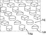
图4描述与本发明的一实施例有关的各种切割元件(16g,16h,16j)。在本发明的一态样中,该切割元件制作(size)并塑型(shape)成具有长方形截面、椭圆截面、圆形截面、三角形、多边形、角锥形截面等。各种被制作并塑型的切割元件能凭借各种切割在该PCD或PcBN片的沟槽的位置以及宽度而形成。该切割元件也能形成在PCD或PcBN片的表面的下(图中未示),以使得该切割元件包括具有例如圆形或多边形的嵌入凹槽(inset cavities)。Figure 4 depicts various cutting elements (16g, 16h, 16j) in relation to an embodiment of the present invention. In one aspect of the invention, the cutting element is sized and shaped to have a rectangular cross-section, an elliptical cross-section, a circular cross-section, a triangular, polygonal, pyramidal cross-section, and the like. Various fabricated and shaped cutting elements can be formed by varying the position and width of the grooves cut in the PCD or PcBN sheet. The cutting element can also be formed under the surface of the PCD or PcBN sheet (not shown in the figure), so that the cutting element comprises inset cavities having eg circular or polygonal shapes.
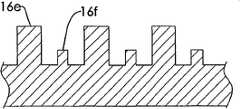
图6A以及图6B描述本发明另一个实施例,其表示形成在一PCD基座的复数切割元件(16e,16f)。从图6A可知,本发明能提供从超硬多晶材料一体成形且具有不同尺寸和配置的切割元件,例如在实施例所显示的,该较大的切割元件(16e)可用于切割、刨平或修整元件,而较小元件(16f)主要是作为「中止(stopping)」元件;换句话说,该较大的切割元件能进一步从该PCD的基座延伸以进一步或更深入地切割正以该切割元件修整的抛光垫(此图未示)。Figures 6A and 6B depict another embodiment of the present invention showing a plurality of cutting elements (16e, 16f) formed on a PCD base. As can be seen from FIG. 6A, the present invention can provide cutting elements integrally formed from superhard polycrystalline materials with different sizes and configurations. For example, as shown in the embodiment, the larger cutting element (16e) can be used for cutting, planing or trimming element, while the smaller element (16f) is primarily a "stopping" element; in other words, the larger cutting element can extend further from the base of the PCD to cut further or deeper into the The cutting element is conditioned by a polishing pad (not shown in this figure).
当该较大切割元件(16e)延伸进工作件内够远或够深时,该较小切割元件能到达工作件的底部的表面(bottom out)以限制该较大切割元件(16e)更深入该工作件中。为有助在达到此概念,可将该较大切割元件制造得比该较小切割元件更尖锐,例如,该较大切割元件能终止在一尖端(与图3C所示的切割元件相似),而该较小切割元件能终止在一平坦的平面(与图3B所示的切割元件相似)。以此方法,该较大切割元件能够比该较小切割元件更容易切割该工作件,以使得该较小切割元件可作为深度「中止」的元件。以此方法,本发明能非常精确地控制该切割元件切入工作件(如被修整的CMP抛光垫)的深度。When the larger cutting element (16e) extends far enough or deep enough into the workpiece, the smaller cutting element can reach the surface (bottom out) of the bottom of the workpiece to limit the larger cutting element (16e) from going deeper in this work piece. To aid in this concept, the larger cutting element can be made sharper than the smaller cutting element, e.g., the larger cutting element can terminate at a tip (similar to the cutting element shown in Figure 3C), Instead, the smaller cutting element can terminate in a flat plane (similar to the cutting element shown in Figure 3B). In this way, the larger cutting element can cut the workpiece more easily than the smaller cutting element, so that the smaller cutting element can act as a depth "stop" element. In this way, the present invention enables very precise control of the depth at which the cutting element cuts into a workpiece, such as a CMP polishing pad being conditioned.
除此之外,当本发明的切割元件能由一整片的多晶超硬材料所形成,则在该切割装置的基座上的切割元件的下保持可用的多晶超硬材料多余的部份(或形成该切割装置的基座)。因此,在本发明的一态样中,一旦切割元件在使用时变钝或被损害,则该切割元件能凭借移除该切割元件整面的一薄的超硬材料层而被削尖(sharpen),并形成与当初在该装置面所产生的一样的图形。只要有足够的多晶材料保持在该切割元件的下,以允许该切割元件进一步削尖,本发明的切割装置能因此相对地易于削尖或修复。In addition, while the cutting element of the present invention can be formed from a single piece of polycrystalline superhard material, there remains a surplus of available polycrystalline superhard material under the cutting element on the base of the cutting device. portion (or form the base of the cutting device). Thus, in one aspect of the invention, once a cutting element becomes dull or damaged in use, the cutting element can be sharpened by removing a thin layer of superhard material from the entire face of the cutting element. ), and form the same graphics as originally produced on the device surface. The cutting device of the present invention can thus be relatively easy to sharpen or repair as long as enough polycrystalline material remains under the cutting element to allow further sharpening of the cutting element.
范例example
以下范例叙述本发明的实施例,因此这些范例不能视为本发明的限制,而是仅适当地教示如何根据本实验数据来实施本发明最佳的系统与方法,因此,系统与方法的代表性数字揭示在此。The following examples describe the embodiments of the present invention, so these examples can not be considered as limitations of the present invention, but only properly teach how to implement the best system and method of the present invention according to the experimental data, therefore, the representativeness of the system and method The numbers are revealed here.
例1:example 1:
一具有烧结的多晶钻石且与胶结碳化钨(cemented tungsten carbide)基材结合的PCD片是作为用于放电加工法(Electrical Discharge Machining,EDM)坯料。该圆盘片具有34mm的直径(如Adico的产品)、52mm(如Adico的产品)、60mm(如Diamond Innovations的产品)、74mm(如Element Six的产品)或100mm(如Tomei Dia的产品)。该典型的PCD层为400-600微米的厚度;总厚度(包括碳化钨基材)如标准材料为1.6mm或3.2mm。A PCD sheet with sintered polycrystalline diamond bonded to a cemented tungsten carbide substrate was used as a blank for Electrical Discharge Machining (EDM). The disk has a diameter of 34 mm (as a product of Adico), 52 mm (as a product of Adico), 60 mm (as a product of Diamond Innovations), 74 mm (as a product of Element Six) or 100 mm (as a product of Tomei Dia). The typical PCD layer is 400-600 microns thick; the total thickness (including tungsten carbide substrate) is 1.6mm or 3.2mm as standard material.
该PCD表面被精细地抛光,以具有一小于约1微米(micron)的Ra值,该坯料是以线切割EDM(wire-EDM)切割以形成锯齿状图形,且顶端至顶点的距离约为400微米,而顶点至凹点的深度约为100微米,其尖端角度为60、70、60、90或100度(相对于施加在抛光垫的磨光表面),其是因为电脑操作截断PCD坯料的不同而不同。该锯齿状图形在被垂直切开的刀片上产生对称的轮廓(profile),该刀片(如切割元件)的厚度能小于约1mm。若所用的线很细(如150微米),则切口的损失就能最小化,而使得各圆盘片的刀片数目最大化。The PCD surface is finely polished to have an Ra value of less than about 1 micron (micron), the blank is cut by wire-EDM to form a zigzag pattern, and the distance from the top to the top is about 400 microns, while the apex-to-dimple depth is about 100 microns, and its tip angle is 60, 70, 60, 90, or 100 degrees (relative to the buffing surface applied to the polishing pad), which is due to the computer operation truncating the PCD blank. It varies from person to person. The serrated pattern creates a symmetrical profile on the vertically slit blade, which blade (eg, cutting element) can be less than about 1 mm thick. If the wire used is very thin (eg 150 microns), then the loss of the kerf can be minimized, thereby maximizing the number of blades per disc.
该刀片能接着以具有微米级钻石悬浮液的超音波水浴清洗,以移除所有悬浮的碎片,以及具有微裂隙(micro crack)和逆转换钻石(back converted diamond)的热剥蚀表面层。The blade can then be cleaned in an ultrasonic water bath with a suspension of micron-sized diamonds to remove all suspended debris, as well as a thermally ablated surface layer with micro cracks and back converted diamonds.
该刀片(如切割元件)能接着固定在一凹槽模具,以对其所有切割尖端在20微米的内。接着,该模具以环氧树脂浇铸以坚固该刀片,以被安排在直径约100mm、而厚度约7mm的圆盘上呈现放射型图案。该刀片能设置有垂直于该模具表面的切割边缘或有一控制的倾斜度。The blade (eg, cutting element) can then be fixed in a recessed mold to within 20 microns of all its cutting tips. Next, the mold was cast with epoxy resin to strengthen the blades to be arranged in a radial pattern on a disc with a diameter of about 100 mm and a thickness of about 7 mm. The blade can be provided with a cutting edge perpendicular to the mold surface or with a controlled inclination.
结果,该切割角度能被调整而在该抛光垫上达到最佳凹槽,也控制在该环氧树脂基材的上的切割尖端突出物(约100微米),该突出物能被排列而使切割尖端的增加平缓,由于如此控制切割扩以及的数量,该抛光垫能被清理,且具有阶梯型表面粗糙度,以达到最佳的抛光效果。As a result, the cutting angle can be adjusted to achieve optimal grooves on the polishing pad, and also to control the cutting tip protrusion (about 100 microns) on the epoxy substrate, which can be aligned to allow cutting The increase in the tip is gentle, and since the amount of cut spread is so controlled, the pad can be cleaned with a stepped surface roughness for optimum polishing.
例如,高的表面粗糙度能快速地清除晶圆上铜沉积的突出点,而能迅速变平坦,令抛光下一个阶梯表面粗糙度以使得铜更薄,最后,该表面粗糙度能变的相对平坦,擦亮(buff)已经很薄的铜层而移除障碍层(如氮化钽(TaN))。目前CMP法需要快速抛光、缓慢抛光以及用三个连续阶段来擦亮。本实用新型的抛光垫调整器能(选择性地)以合一的阶段操作,而大大地节省制作成本并促进产品的生产率。For example, a high surface roughness can quickly clear the protruding spots of copper deposition on the wafer, which can be flattened quickly, allowing polishing the next step surface roughness to make the copper thinner, and finally, the surface roughness can become relatively Flatten, buff the already thin copper layer and remove the barrier layer (such as tantalum nitride (TaN)). Current CMP methods require fast polishing, slow polishing, and polishing in three consecutive stages. The polishing pad adjuster of the present invention can (selectively) be operated in one stage, thereby greatly saving the manufacturing cost and promoting the productivity of the product.
一旦上述的尖端变钝,而使得在抛光晶圆时降低移除率,则所使用的尖端能简单地恢复凭借溶解在溶剂中或烧掉环氧树脂基材,该刀片能接着重新设定为具有另一个锯齿状侧边以制造新的抛光垫调整器,此能大大地降低制造成本。既有的抛光垫调整器因为无法从尖锐的尖端挑选出磨损的尖端而很少重新被使用。Once the aforementioned tip becomes blunt, reducing the removal rate when polishing the wafer, the tip used can simply be restored by dissolving in a solvent or burning off the epoxy substrate, the blade can then be reset to Having another serrated side to create a new pad conditioner can greatly reduce manufacturing costs. Existing pad conditioners are rarely reused because of the inability to pick out worn tips from sharp ones.
例2:Example 2:
使用与例1中所述相似的方法,不同的处在于以碳化钨坯料代替PCD。该碳化钨坯料包括少量的钴(如6wt%),将直的刀片设置在一固定装置,且放置在一具有甲烷(1%)与氢的混合物的CVD反应器,该具甲烷与氢的混合物能热分解且分离成碳和原子氢。该涂布有碳化钨的CVDD将沉积在钻石颗粒,凭借控制成核密度、稀疏的原子核分布、较大的颗粒、较高的突出物以及更远的分隔率来间隔尖锐切割尖端。该钻石颗粒的范围能从奈米结晶(如直的边缘)至大于10微米的颗粒。在碳化钨中低的钴含量能帮助钻石避免因其触媒能力所产生的逆反应而得以保存。A method similar to that described in Example 1 was used except that a tungsten carbide blank was used instead of PCD. The tungsten carbide blank includes a small amount of cobalt (eg, 6 wt%), the straight blade is set in a fixture, and placed in a CVD reactor with a mixture of methane (1%) and hydrogen, the mixture of methane and hydrogen Can be thermally decomposed and separated into carbon and atomic hydrogen. The tungsten carbide coated CVDD will be deposited on the diamond grains to space the sharp cutting tips with controlled nucleation density, sparser nuclei distribution, larger grains, higher protrusions and farther separation ratios. The diamond particles can range from nanocrystalline (eg, straight edges) to particles larger than 10 microns. The low cobalt content in tungsten carbide helps diamonds to be preserved from the reverse reaction caused by its catalytic ability.
例3:Example 3:
使用与例2所述相似的步骤,不同的处在于该刀片是从掺杂碳化硅坯料的硅所切片形成的。A procedure similar to that described in Example 2 was used, except that the inserts were sliced from silicon doped silicon carbide ingots.
例4:Example 4:
使用与例3所述相似的步骤,不同的处在于该刀片是从一烧结的微米级的粒状氮化硅所切片形成的。A procedure similar to that described in Example 3 was used, except that the inserts were sliced from a sintered micron-sized granular silicon nitride.
例5:Example 5:
使用与例2所述相似的步骤,不同的处在于也可使用由具有钇强化氧化锆(ZrO2)以及钛所制成的胚料,以作为钻石薄膜沉积所用的界面涂布缓冲剂。A procedure similar to that described in Example 2 was used, except that blanks made with yttrium-strengthened zirconia (ZrO2) and titanium were also used as interfacial coating buffers for diamond film deposition.
需要了解的是,以上该排列都仅是在描述本发明原则的应用,许多改变以及不同的排列也可以在不脱离本发明的精神和范围的情况下被在本领域技术人员所设想出来,而保护范围也涵盖上述的改变和排列。因此,尽管本发明被特定以及详述地描述呈上述最实用和最佳实施例,在本领域技术人员可在不偏离本发明的原则和观点的情况下做许多如尺寸、材料、形状、样式、功能、操作方法、组装和使用等变动。It should be understood that the above arrangement is only to describe the application of the principles of the present invention, and many changes and different arrangements can also be conceived by those skilled in the art without departing from the spirit and scope of the present invention. The scope of protection also covers modifications and permutations of the above. Therefore, although the present invention has been specifically and detailedly described as the above-mentioned most practical and preferred embodiment, those skilled in the art can make many changes such as size, material, shape, style without departing from the principles and viewpoints of the present invention. , function, method of operation, assembly and use.
Claims (25)
Translated fromChineseApplications Claiming Priority (2)
| Application Number | Priority Date | Filing Date | Title |
|---|---|---|---|
| US86620206P | 2006-11-16 | 2006-11-16 | |
| US60/866,202 | 2006-11-16 |
Publications (1)
| Publication Number | Publication Date |
|---|---|
| CN101557904Atrue CN101557904A (en) | 2009-10-14 |
Family
ID=39536874
Family Applications (1)
| Application Number | Title | Priority Date | Filing Date |
|---|---|---|---|
| CNA2007800463355APendingCN101557904A (en) | 2006-11-16 | 2007-11-16 | CMP pad conditioner and associated methods |
Country Status (4)
| Country | Link |
|---|---|
| US (1) | US20080153398A1 (en) |
| CN (1) | CN101557904A (en) |
| TW (1) | TWI356449B (en) |
| WO (1) | WO2008076199A2 (en) |
Cited By (5)
| Publication number | Priority date | Publication date | Assignee | Title |
|---|---|---|---|---|
| CN103688343A (en)* | 2011-03-07 | 2014-03-26 | 恩特格里公司 | Chemical mechanical planarization pad conditioner |
| CN104755236A (en)* | 2012-10-19 | 2015-07-01 | 陶氏环球技术有限公司 | Apparatus and method for cutting formable and/or shrinkable material |
| CN106078517A (en)* | 2016-08-03 | 2016-11-09 | 咏巨科技有限公司 | Polishing pad dressing device |
| CN106463379A (en)* | 2014-03-21 | 2017-02-22 | 恩特格里斯公司 | Chemical mechanical planarization pad conditioner with elongated cutting edges |
| TWI884897B (en)* | 2025-01-23 | 2025-05-21 | 日鐵精工股份有限公司 | Stable polishing pad conditioner |
Families Citing this family (35)
| Publication number | Priority date | Publication date | Assignee | Title |
|---|---|---|---|---|
| US9199357B2 (en) | 1997-04-04 | 2015-12-01 | Chien-Min Sung | Brazed diamond tools and methods for making the same |
| US9868100B2 (en) | 1997-04-04 | 2018-01-16 | Chien-Min Sung | Brazed diamond tools and methods for making the same |
| US9409280B2 (en) | 1997-04-04 | 2016-08-09 | Chien-Min Sung | Brazed diamond tools and methods for making the same |
| US9238207B2 (en) | 1997-04-04 | 2016-01-19 | Chien-Min Sung | Brazed diamond tools and methods for making the same |
| US9463552B2 (en) | 1997-04-04 | 2016-10-11 | Chien-Min Sung | Superbrasvie tools containing uniformly leveled superabrasive particles and associated methods |
| US9221154B2 (en) | 1997-04-04 | 2015-12-29 | Chien-Min Sung | Diamond tools and methods for making the same |
| US7516536B2 (en)* | 1999-07-08 | 2009-04-14 | Toho Engineering Kabushiki Kaisha | Method of producing polishing pad |
| US9724802B2 (en) | 2005-05-16 | 2017-08-08 | Chien-Min Sung | CMP pad dressers having leveled tips and associated methods |
| US8678878B2 (en) | 2009-09-29 | 2014-03-25 | Chien-Min Sung | System for evaluating and/or improving performance of a CMP pad dresser |
| US8393934B2 (en) | 2006-11-16 | 2013-03-12 | Chien-Min Sung | CMP pad dressers with hybridized abrasive surface and related methods |
| US9138862B2 (en) | 2011-05-23 | 2015-09-22 | Chien-Min Sung | CMP pad dresser having leveled tips and associated methods |
| US8398466B2 (en) | 2006-11-16 | 2013-03-19 | Chien-Min Sung | CMP pad conditioners with mosaic abrasive segments and associated methods |
| US8622787B2 (en) | 2006-11-16 | 2014-01-07 | Chien-Min Sung | CMP pad dressers with hybridized abrasive surface and related methods |
| US20150017884A1 (en)* | 2006-11-16 | 2015-01-15 | Chien-Min Sung | CMP Pad Dressers with Hybridized Abrasive Surface and Related Methods |
| JP2010536183A (en) | 2007-08-23 | 2010-11-25 | サンーゴバン アブレイシブズ,インコーポレイティド | Optimized CMP conditioner design for next generation oxide / metal CMP |
| TW200940258A (en)* | 2007-11-13 | 2009-10-01 | Chien-Min Sung | CMP pad dressers |
| TWI388402B (en)* | 2007-12-06 | 2013-03-11 | Methods for orienting superabrasive particles on a surface and associated tools | |
| TWI473685B (en)* | 2008-01-15 | 2015-02-21 | Iv Technologies Co Ltd | Polishing pad and fabricating method thereof |
| KR101413030B1 (en) | 2009-03-24 | 2014-07-02 | 생-고벵 아브라시프 | Abrasive tool for use as a chemical mechanical planarization pad conditioner |
| US8905823B2 (en) | 2009-06-02 | 2014-12-09 | Saint-Gobain Abrasives, Inc. | Corrosion-resistant CMP conditioning tools and methods for making and using same |
| NL1037020C2 (en)* | 2009-06-05 | 2010-12-07 | Auto Cosmetics Hoogeveen | TOOLS AND METHOD FOR RECONDITIONING A POLISHING PATH, ALSO METHOD FOR MANUFACTURING SUCH A TOOL. |
| WO2011028700A2 (en) | 2009-09-01 | 2011-03-10 | Saint-Gobain Abrasives, Inc. | Chemical mechanical polishing conditioner |
| KR101091030B1 (en)* | 2010-04-08 | 2011-12-09 | 이화다이아몬드공업 주식회사 | Method for producing pad conditioner having reduced friction |
| WO2012162430A2 (en) | 2011-05-23 | 2012-11-29 | Chien-Min Sung | Cmp pad dresser having leveled tips and associated methods |
| CN102229105A (en)* | 2011-06-28 | 2011-11-02 | 清华大学 | Chemically mechanical polishing method |
| KR101339722B1 (en)* | 2011-07-18 | 2013-12-10 | 이화다이아몬드공업 주식회사 | CMP Pad conditioner |
| WO2013166516A1 (en)* | 2012-05-04 | 2013-11-07 | Entegris, Inc. | Cmp conditioner pads with superabrasive grit enhancement |
| EP2879838B1 (en) | 2012-08-02 | 2023-09-13 | 3M Innovative Properties Company | Abrasive articles with precisely shaped features and method of making thereof |
| EP2879837B1 (en) | 2012-08-02 | 2018-09-19 | 3M Innovative Properties Company | Abrasive element precursor with precisely shaped features and method of making thereof |
| US9457450B2 (en) | 2013-03-08 | 2016-10-04 | Tera Xtal Technology Corporation | Pad conditioning tool |
| TWI511841B (en)* | 2013-03-15 | 2015-12-11 | Kinik Co | Stick-type chemical mechanical polishing conditioner and manufacturing method thereof |
| EP3843946A1 (en)* | 2018-08-31 | 2021-07-07 | Best Engineered Surface Technologies, LLC | Hybrid cmp conditioning head |
| US20250050464A1 (en)* | 2021-12-31 | 2025-02-13 | 3M Innovative Properties Company | Conditioning disk with microfeatures |
| KR102804527B1 (en)* | 2022-07-20 | 2025-05-12 | 새솔다이아몬드공업 주식회사 | Pad conditioner |
| CN117103123B (en)* | 2023-10-24 | 2024-01-30 | 华南理工大学 | A micro-nano structure forming control method for diamond abrasive grain smoothing surface |
Family Cites Families (55)
| Publication number | Priority date | Publication date | Assignee | Title |
|---|---|---|---|---|
| US621856A (en)* | 1899-03-28 | Jacob schwarz | ||
| US3852078A (en)* | 1970-12-24 | 1974-12-03 | M Wakatsuki | Mass of polycrystalline cubic system boron nitride and composites of polycrystalline cubic system boron nitride and other hard materials, and processes for manufacturing the same |
| US4554139A (en)* | 1983-09-27 | 1985-11-19 | Prodeco, Inc. | Process for producing and decomposing syngenite |
| US4923490A (en)* | 1988-12-16 | 1990-05-08 | General Electric Company | Novel grinding wheels utilizing polycrystalline diamond or cubic boron nitride grit |
| US4925457B1 (en)* | 1989-01-30 | 1995-09-26 | Ultimate Abrasive Syst Inc | Method for making an abrasive tool |
| US5049165B1 (en)* | 1989-01-30 | 1995-09-26 | Ultimate Abrasive Syst Inc | Composite material |
| GB9006703D0 (en)* | 1990-03-26 | 1990-05-23 | De Beers Ind Diamond | Abrasive product |
| US5380390B1 (en)* | 1991-06-10 | 1996-10-01 | Ultimate Abras Systems Inc | Patterned abrasive material and method |
| US5247765A (en)* | 1991-07-23 | 1993-09-28 | Abrasive Technology Europe, S.A. | Abrasive product comprising a plurality of discrete composite abrasive pellets in a resilient resin matrix |
| JPH0639729A (en)* | 1992-05-29 | 1994-02-15 | Canon Inc | Fine grinding wheel and method for manufacturing the same |
| GB9310500D0 (en)* | 1993-05-21 | 1993-07-07 | De Beers Ind Diamond | Cutting tool |
| WO1995000295A1 (en)* | 1993-06-17 | 1995-01-05 | Minnesota Mining And Manufacturing Company | Patterned abrading articles and methods making and using same |
| US5681612A (en)* | 1993-06-17 | 1997-10-28 | Minnesota Mining And Manufacturing Company | Coated abrasives and methods of preparation |
| US5453106A (en)* | 1993-10-27 | 1995-09-26 | Roberts; Ellis E. | Oriented particles in hard surfaces |
| US5486131A (en)* | 1994-01-04 | 1996-01-23 | Speedfam Corporation | Device for conditioning polishing pads |
| US5547417A (en)* | 1994-03-21 | 1996-08-20 | Intel Corporation | Method and apparatus for conditioning a semiconductor polishing pad |
| US5536202A (en)* | 1994-07-27 | 1996-07-16 | Texas Instruments Incorporated | Semiconductor substrate conditioning head having a plurality of geometries formed in a surface thereof for pad conditioning during chemical-mechanical polish |
| MX9702267A (en)* | 1994-09-30 | 1997-06-28 | Minnesota Mining & Mfg | Coated abrasive article, method for preparing the same, and method of using. |
| US5527424A (en)* | 1995-01-30 | 1996-06-18 | Motorola, Inc. | Preconditioner for a polishing pad and method for using the same |
| US5560754A (en)* | 1995-06-13 | 1996-10-01 | General Electric Company | Reduction of stresses in the polycrystalline abrasive layer of a composite compact with in situ bonded carbide/carbide support |
| US6371838B1 (en)* | 1996-07-15 | 2002-04-16 | Speedfam-Ipec Corporation | Polishing pad conditioning device with cutting elements |
| WO1998016347A1 (en)* | 1996-10-15 | 1998-04-23 | Nippon Steel Corporation | Semiconductor substrate polishing pad dresser, method of manufacturing the same, and chemicomechanical polishing method using the same dresser |
| US7491116B2 (en)* | 2004-09-29 | 2009-02-17 | Chien-Min Sung | CMP pad dresser with oriented particles and associated methods |
| US6368198B1 (en)* | 1999-11-22 | 2002-04-09 | Kinik Company | Diamond grid CMP pad dresser |
| US5921855A (en)* | 1997-05-15 | 1999-07-13 | Applied Materials, Inc. | Polishing pad having a grooved pattern for use in a chemical mechanical polishing system |
| JP3244454B2 (en)* | 1997-06-05 | 2002-01-07 | 理化学研究所 | Cutting and grinding dual use tool |
| US5921856A (en)* | 1997-07-10 | 1999-07-13 | Sp3, Inc. | CVD diamond coated substrate for polishing pad conditioning head and method for making same |
| US6027659A (en)* | 1997-12-03 | 2000-02-22 | Intel Corporation | Polishing pad conditioning surface having integral conditioning points |
| US6159087A (en)* | 1998-02-11 | 2000-12-12 | Applied Materials, Inc. | End effector for pad conditioning |
| CA2261491C (en)* | 1998-03-06 | 2005-05-24 | Smith International, Inc. | Cutting element with improved polycrystalline material toughness and method for making same |
| JP3295888B2 (en)* | 1998-04-22 | 2002-06-24 | 株式会社藤森技術研究所 | Polishing dresser for polishing machine of chemical machine polisher |
| KR19990081117A (en)* | 1998-04-25 | 1999-11-15 | 윤종용 | CMP Pad Conditioning Disc and Conditioner, Manufacturing Method, Regeneration Method and Cleaning Method of the Disc |
| US6354918B1 (en)* | 1998-06-19 | 2002-03-12 | Ebara Corporation | Apparatus and method for polishing workpiece |
| US6299508B1 (en)* | 1998-08-05 | 2001-10-09 | 3M Innovative Properties Company | Abrasive article with integrally molded front surface protrusions containing a grinding aid and methods of making and using |
| US6346202B1 (en)* | 1999-03-25 | 2002-02-12 | Beaver Creek Concepts Inc | Finishing with partial organic boundary layer |
| KR20000056068A (en)* | 1999-02-12 | 2000-09-15 | 윤종용 | Disk of pad conditioner |
| EP1075898A3 (en)* | 1999-08-13 | 2003-11-05 | Mitsubishi Materials Corporation | Dresser and dressing apparatus |
| US6281129B1 (en)* | 1999-09-20 | 2001-08-28 | Agere Systems Guardian Corp. | Corrosion-resistant polishing pad conditioner |
| TW467802B (en)* | 1999-10-12 | 2001-12-11 | Hunatech Co Ltd | Conditioner for polishing pad and method for manufacturing the same |
| JP3527448B2 (en)* | 1999-12-20 | 2004-05-17 | 株式会社リード | Dresser for CMP polishing cloth and its manufacturing method |
| KR100853060B1 (en)* | 2000-08-08 | 2008-08-19 | 엘리먼트 씩스 (프티) 리미티드 | How to produce abrasive products containing diamond |
| WO2002028598A1 (en)* | 2000-10-02 | 2002-04-11 | Rodel Holdings, Inc. | Method for conditioning polishing pads |
| US20030207659A1 (en)* | 2000-11-03 | 2003-11-06 | 3M Innovative Properties Company | Abrasive product and method of making and using the same |
| US8545583B2 (en)* | 2000-11-17 | 2013-10-01 | Wayne O. Duescher | Method of forming a flexible abrasive sheet article |
| US6672943B2 (en)* | 2001-01-26 | 2004-01-06 | Wafer Solutions, Inc. | Eccentric abrasive wheel for wafer processing |
| KR100428947B1 (en)* | 2001-09-28 | 2004-04-29 | 이화다이아몬드공업 주식회사 | Diamond Tool |
| KR100449630B1 (en)* | 2001-11-13 | 2004-09-22 | 삼성전기주식회사 | Apparatus for conditioning a polishing pad used in a chemical-mechanical polishing system |
| US6872127B2 (en)* | 2002-07-11 | 2005-03-29 | Taiwan Semiconductor Manufacturing Co., Ltd | Polishing pad conditioning disks for chemical mechanical polisher |
| US20050060941A1 (en)* | 2003-09-23 | 2005-03-24 | 3M Innovative Properties Company | Abrasive article and methods of making the same |
| US20070060026A1 (en)* | 2005-09-09 | 2007-03-15 | Chien-Min Sung | Methods of bonding superabrasive particles in an organic matrix |
| US20060258276A1 (en)* | 2005-05-16 | 2006-11-16 | Chien-Min Sung | Superhard cutters and associated methods |
| US7150677B2 (en)* | 2004-09-22 | 2006-12-19 | Mitsubishi Materials Corporation | CMP conditioner |
| US7066795B2 (en)* | 2004-10-12 | 2006-06-27 | Applied Materials, Inc. | Polishing pad conditioner with shaped abrasive patterns and channels |
| US7300338B2 (en)* | 2005-09-22 | 2007-11-27 | Abrasive Technology, Inc. | CMP diamond conditioning disk |
| US7594845B2 (en)* | 2005-10-20 | 2009-09-29 | 3M Innovative Properties Company | Abrasive article and method of modifying the surface of a workpiece |
- 2007
- 2007-11-15USUS11/940,935patent/US20080153398A1/ennot_activeAbandoned
- 2007-11-16TWTW096143400Apatent/TWI356449B/ennot_activeIP Right Cessation
- 2007-11-16CNCNA2007800463355Apatent/CN101557904A/enactivePending
- 2007-11-16WOPCT/US2007/024169patent/WO2008076199A2/enactiveApplication Filing
Cited By (6)
| Publication number | Priority date | Publication date | Assignee | Title |
|---|---|---|---|---|
| CN103688343A (en)* | 2011-03-07 | 2014-03-26 | 恩特格里公司 | Chemical mechanical planarization pad conditioner |
| CN103688343B (en)* | 2011-03-07 | 2016-09-07 | 恩特格里公司 | Chemical mechanical polishing dresser |
| CN104755236A (en)* | 2012-10-19 | 2015-07-01 | 陶氏环球技术有限公司 | Apparatus and method for cutting formable and/or shrinkable material |
| CN106463379A (en)* | 2014-03-21 | 2017-02-22 | 恩特格里斯公司 | Chemical mechanical planarization pad conditioner with elongated cutting edges |
| CN106078517A (en)* | 2016-08-03 | 2016-11-09 | 咏巨科技有限公司 | Polishing pad dressing device |
| TWI884897B (en)* | 2025-01-23 | 2025-05-21 | 日鐵精工股份有限公司 | Stable polishing pad conditioner |
Also Published As
| Publication number | Publication date |
|---|---|
| US20080153398A1 (en) | 2008-06-26 |
| WO2008076199A2 (en) | 2008-06-26 |
| TWI356449B (en) | 2012-01-11 |
| TW200837823A (en) | 2008-09-16 |
| WO2008076199A3 (en) | 2008-08-21 |
Similar Documents
| Publication | Publication Date | Title |
|---|---|---|
| CN101557904A (en) | CMP pad conditioner and associated methods | |
| CN101903131B (en) | CMP pad conditioner | |
| CN101856806B (en) | Superabrasive tool with surface-modified diamond particles and related methods | |
| US7658666B2 (en) | Superhard cutters and associated methods | |
| US20190091832A1 (en) | Composite conditioner and associated methods | |
| CN104303270B (en) | cutting knife | |
| US7762872B2 (en) | Superhard cutters and associated methods | |
| US20060258276A1 (en) | Superhard cutters and associated methods | |
| CN102066283B (en) | Ceramic abrasive with extremely low bulk density, method of manufacture and use thereof | |
| TWI355986B (en) | Superhard cutters and associated methods | |
| TWI632601B (en) | Dual dressing system for cmp pads and associated methods | |
| CN101094746A (en) | CMP pad dresser | |
| JP2009502533A5 (en) | ||
| WO2002022310A1 (en) | Ultra abrasive grain wheel for mirror finish | |
| Pal et al. | Development and performance evaluation of monolayer brazed cBN grinding wheel on bearing steel | |
| CN112677061B (en) | Brazing diamond grinding disc for steel grinding and preparation method thereof | |
| CN101137463A (en) | Superhard cutting device and method of making same | |
| JP6578985B2 (en) | Substrate, substrate cutting method | |
| JPH04135176A (en) | Dressing method for poreless type grinding wheel | |
| Sung et al. | PCD pad conditioners for low pressure chemical mechanical planarisation of semiconductors | |
| JPH11216675A (en) | High precision super abrasive wheel | |
| JP2004167655A (en) | Whetstone for rotary ultrasonic machining | |
| Chen et al. | Diamond Pad Conditioners with Oriented Polycrystalline Diamond Cubes |
Legal Events
| Date | Code | Title | Description |
|---|---|---|---|
| C06 | Publication | ||
| PB01 | Publication | ||
| C10 | Entry into substantive examination | ||
| SE01 | Entry into force of request for substantive examination | ||
| C02 | Deemed withdrawal of patent application after publication (patent law 2001) | ||
| WD01 | Invention patent application deemed withdrawn after publication | Application publication date:20091014 |