CN101556418A - Liquid crystal display device - Google Patents
Liquid crystal display deviceDownload PDFInfo
- Publication number
- CN101556418A CN101556418ACNA200810178146XACN200810178146ACN101556418ACN 101556418 ACN101556418 ACN 101556418ACN A200810178146X ACNA200810178146X ACN A200810178146XACN 200810178146 ACN200810178146 ACN 200810178146ACN 101556418 ACN101556418 ACN 101556418A
- Authority
- CN
- China
- Prior art keywords
- liquid crystal
- substrate
- capacitor
- electrode
- pixel
- Prior art date
- Legal status (The legal status is an assumption and is not a legal conclusion. Google has not performed a legal analysis and makes no representation as to the accuracy of the status listed.)
- Granted
Links
Images


Classifications
- G—PHYSICS
- G09—EDUCATION; CRYPTOGRAPHY; DISPLAY; ADVERTISING; SEALS
- G09G—ARRANGEMENTS OR CIRCUITS FOR CONTROL OF INDICATING DEVICES USING STATIC MEANS TO PRESENT VARIABLE INFORMATION
- G09G3/00—Control arrangements or circuits, of interest only in connection with visual indicators other than cathode-ray tubes
- G09G3/20—Control arrangements or circuits, of interest only in connection with visual indicators other than cathode-ray tubes for presentation of an assembly of a number of characters, e.g. a page, by composing the assembly by combination of individual elements arranged in a matrix no fixed position being assigned to or needed to be assigned to the individual characters or partial characters
- G09G3/34—Control arrangements or circuits, of interest only in connection with visual indicators other than cathode-ray tubes for presentation of an assembly of a number of characters, e.g. a page, by composing the assembly by combination of individual elements arranged in a matrix no fixed position being assigned to or needed to be assigned to the individual characters or partial characters by control of light from an independent source
- G09G3/36—Control arrangements or circuits, of interest only in connection with visual indicators other than cathode-ray tubes for presentation of an assembly of a number of characters, e.g. a page, by composing the assembly by combination of individual elements arranged in a matrix no fixed position being assigned to or needed to be assigned to the individual characters or partial characters by control of light from an independent source using liquid crystals
- G09G3/3611—Control of matrices with row and column drivers
- G09G3/3648—Control of matrices with row and column drivers using an active matrix
- G—PHYSICS
- G01—MEASURING; TESTING
- G01L—MEASURING FORCE, STRESS, TORQUE, WORK, MECHANICAL POWER, MECHANICAL EFFICIENCY, OR FLUID PRESSURE
- G01L1/00—Measuring force or stress, in general
- G01L1/14—Measuring force or stress, in general by measuring variations in capacitance or inductance of electrical elements, e.g. by measuring variations of frequency of electrical oscillators
- G—PHYSICS
- G02—OPTICS
- G02F—OPTICAL DEVICES OR ARRANGEMENTS FOR THE CONTROL OF LIGHT BY MODIFICATION OF THE OPTICAL PROPERTIES OF THE MEDIA OF THE ELEMENTS INVOLVED THEREIN; NON-LINEAR OPTICS; FREQUENCY-CHANGING OF LIGHT; OPTICAL LOGIC ELEMENTS; OPTICAL ANALOGUE/DIGITAL CONVERTERS
- G02F1/00—Devices or arrangements for the control of the intensity, colour, phase, polarisation or direction of light arriving from an independent light source, e.g. switching, gating or modulating; Non-linear optics
- G02F1/01—Devices or arrangements for the control of the intensity, colour, phase, polarisation or direction of light arriving from an independent light source, e.g. switching, gating or modulating; Non-linear optics for the control of the intensity, phase, polarisation or colour
- G02F1/13—Devices or arrangements for the control of the intensity, colour, phase, polarisation or direction of light arriving from an independent light source, e.g. switching, gating or modulating; Non-linear optics for the control of the intensity, phase, polarisation or colour based on liquid crystals, e.g. single liquid crystal display cells
- G02F1/133—Constructional arrangements; Operation of liquid crystal cells; Circuit arrangements
- G—PHYSICS
- G09—EDUCATION; CRYPTOGRAPHY; DISPLAY; ADVERTISING; SEALS
- G09G—ARRANGEMENTS OR CIRCUITS FOR CONTROL OF INDICATING DEVICES USING STATIC MEANS TO PRESENT VARIABLE INFORMATION
- G09G3/00—Control arrangements or circuits, of interest only in connection with visual indicators other than cathode-ray tubes
- G09G3/20—Control arrangements or circuits, of interest only in connection with visual indicators other than cathode-ray tubes for presentation of an assembly of a number of characters, e.g. a page, by composing the assembly by combination of individual elements arranged in a matrix no fixed position being assigned to or needed to be assigned to the individual characters or partial characters
- G—PHYSICS
- G02—OPTICS
- G02F—OPTICAL DEVICES OR ARRANGEMENTS FOR THE CONTROL OF LIGHT BY MODIFICATION OF THE OPTICAL PROPERTIES OF THE MEDIA OF THE ELEMENTS INVOLVED THEREIN; NON-LINEAR OPTICS; FREQUENCY-CHANGING OF LIGHT; OPTICAL LOGIC ELEMENTS; OPTICAL ANALOGUE/DIGITAL CONVERTERS
- G02F1/00—Devices or arrangements for the control of the intensity, colour, phase, polarisation or direction of light arriving from an independent light source, e.g. switching, gating or modulating; Non-linear optics
- G02F1/01—Devices or arrangements for the control of the intensity, colour, phase, polarisation or direction of light arriving from an independent light source, e.g. switching, gating or modulating; Non-linear optics for the control of the intensity, phase, polarisation or colour
- G02F1/13—Devices or arrangements for the control of the intensity, colour, phase, polarisation or direction of light arriving from an independent light source, e.g. switching, gating or modulating; Non-linear optics for the control of the intensity, phase, polarisation or colour based on liquid crystals, e.g. single liquid crystal display cells
- G02F1/133—Constructional arrangements; Operation of liquid crystal cells; Circuit arrangements
- G02F1/1333—Constructional arrangements; Manufacturing methods
- G02F1/13338—Input devices, e.g. touch panels
- G—PHYSICS
- G09—EDUCATION; CRYPTOGRAPHY; DISPLAY; ADVERTISING; SEALS
- G09G—ARRANGEMENTS OR CIRCUITS FOR CONTROL OF INDICATING DEVICES USING STATIC MEANS TO PRESENT VARIABLE INFORMATION
- G09G2300/00—Aspects of the constitution of display devices
- G09G2300/04—Structural and physical details of display devices
- G09G2300/0421—Structural details of the set of electrodes
- G09G2300/0426—Layout of electrodes and connections
- G—PHYSICS
- G09—EDUCATION; CRYPTOGRAPHY; DISPLAY; ADVERTISING; SEALS
- G09G—ARRANGEMENTS OR CIRCUITS FOR CONTROL OF INDICATING DEVICES USING STATIC MEANS TO PRESENT VARIABLE INFORMATION
- G09G2300/00—Aspects of the constitution of display devices
- G09G2300/04—Structural and physical details of display devices
- G09G2300/0439—Pixel structures
- G09G2300/0452—Details of colour pixel setup, e.g. pixel composed of a red, a blue and two green components
Landscapes
- Physics & Mathematics (AREA)
- Engineering & Computer Science (AREA)
- General Physics & Mathematics (AREA)
- Computer Hardware Design (AREA)
- Theoretical Computer Science (AREA)
- Chemical & Material Sciences (AREA)
- Crystallography & Structural Chemistry (AREA)
- Nonlinear Science (AREA)
- Liquid Crystal (AREA)
- Mathematical Physics (AREA)
- Optics & Photonics (AREA)
- Position Input By Displaying (AREA)
Abstract
Description
Translated fromChinese技术领域technical field
本发明涉及液晶显示装置,更具体地涉及一种用于识别由于接触而造成的液晶电容的变化从而能够感测装置是否被接触以及接触区域的位置的液晶显示装置。The present invention relates to a liquid crystal display device, and more particularly, to a liquid crystal display device for recognizing a change in capacitance of a liquid crystal due to a touch so as to be able to sense whether the device is touched and a position of a touch area.
背景技术Background technique
随着信息时代的来临,可视地表示电子数据信号的显示器领域得到快速增长,并且为了满足这种增长,已经开发出了具有例如外形薄、重量轻和功耗低的卓越特性的各种平板显示装置,并且迅速取代了常规的阴极射线管(CRT)。With the advent of the information age, the field of displays that visually represent electronic data signals has grown rapidly, and in order to meet this growth, various flat panels having excellent characteristics such as thin profile, light weight, and low power consumption have been developed Display devices, and are rapidly replacing conventional cathode ray tubes (CRTs).
具体来讲,平板显示装置包括液晶显示装置(LCD)、等离子体显示板装置(PDP)、场致发射显示装置(FED)、电致发光显示装置(ELD)等。以上所有平板显示装置实质上都包括用于显示图像的平板显示板。平板显示板由一对透明的绝缘基板组成,这一对绝缘基板在其间插入有本征发光或偏振材料层的情况下彼此结合。Specifically, the flat panel display device includes a liquid crystal display device (LCD), a plasma display panel device (PDP), a field emission display device (FED), an electroluminescent display device (ELD), and the like. All of the above flat display devices essentially include a flat display panel for displaying images. Flat panel display panels consist of a pair of transparent insulating substrates bonded to each other with a layer of intrinsically luminescent or polarizing material interposed therebetween.
在以上平板显示装置当中,液晶显示装置通过利用电场来调节液晶的透光率而显示图像。因此,液晶显示器包括具有多个液晶单元的显示板、用于向该显示板照射光的背光单元以及用于驱动这些液晶单元的驱动电路。Among the above flat panel display devices, the liquid crystal display device displays images by adjusting light transmittance of liquid crystals using an electric field. Accordingly, a liquid crystal display includes a display panel having a plurality of liquid crystal cells, a backlight unit for irradiating light to the display panel, and a driving circuit for driving the liquid crystal cells.
显示板被构造为,多条选通线和多条数据线相互交叉,限定了多个单元像素区。这里,在每个像素区中都设置有彼此相对的薄膜晶体管阵列基板和滤色器基板、被放置用于在这两个基板之间维持指定单元间隙的间隔体,以及填充该单元间隙的液晶。The display panel is structured such that a plurality of gate lines and a plurality of data lines intersect each other to define a plurality of unit pixel regions. Here, a thin film transistor array substrate and a color filter substrate facing each other, a spacer placed to maintain a prescribed cell gap between these two substrates, and a liquid crystal filling the cell gap are provided in each pixel region. .
薄膜晶体管阵列基板包括选通线和数据线、充当开关元件并且形成在选通线和数据线的交叉点处的薄膜晶体管、以液晶单元为单位形成并且连接到薄膜晶体管的像素电极,以及涂覆在其上的配向层。选通线和数据线分别通过它们的焊点部件从驱动电路接收信号。The thin film transistor array substrate includes gate lines and data lines, thin film transistors serving as switching elements and formed at intersections of the gate lines and data lines, pixel electrodes formed in units of liquid crystal cells and connected to the thin film transistors, and coating Alignment layer on it. The gate lines and the data lines receive signals from the driving circuit through their pad parts, respectively.
薄膜晶体管对供应给选通线的扫描信号作出响应,由此将供应给数据线的像素电压信号供应给像素电极。The thin film transistor responds to the scan signal supplied to the gate line, thereby supplying the pixel voltage signal supplied to the data line to the pixel electrode.
滤色器阵列基板包括以液晶单元为单位形成的滤色器、用于将滤色器彼此分开并反射外部光的黑底、用于向液晶单元共同地供应参考电压的公共电极,以及涂覆在其上的配向层。The color filter array substrate includes color filters formed in units of liquid crystal cells, a black matrix for separating the color filters from each other and reflecting external light, a common electrode for commonly supplying a reference voltage to the liquid crystal cells, and coating Alignment layer on it.
将分别制造的薄膜晶体管阵列基板和滤色器阵列基板对准,然后将它们彼此结合。然后,在两个基板之间的间隙中填充液晶并密封该间隙,由此完成了显示板。The separately manufactured thin film transistor array substrate and color filter array substrate are aligned and then bonded to each other. Then, liquid crystal is filled in the gap between the two substrates and the gap is sealed, thereby completing the display panel.
在按上述工艺制造的液晶显示装置中,对于触摸板的需求已经增大,该触摸板识别通过手或单独的输入单元接触的区域的位置并且相应地发送单独的数据。该触摸板目前用在这样的情况下,即,触摸板附接在液晶显示装置的外表面上。因此,已进行了将触摸板安装在液晶显示装置中的板内的尝试。In the liquid crystal display devices manufactured in the above process, the demand has increased for a touch panel that recognizes the position of an area touched by a hand or a separate input unit and transmits separate data accordingly. The touch panel is currently used in a case where the touch panel is attached to the outer surface of the liquid crystal display device. Therefore, attempts have been made to mount a touch panel within a panel in a liquid crystal display device.
现在来描述液晶显示装置的例子,其中安装了以上触摸板来防止由于在液晶显示装置的外表面附接一单独的触摸板而造成的体积增大。Now, an example of a liquid crystal display device is described in which the above touch panel is mounted to prevent bulk increase due to the attachment of a separate touch panel on the outer surface of the liquid crystal display device.
以下,将参照附图来描述常规的液晶显示装置。Hereinafter, a conventional liquid crystal display device will be described with reference to the accompanying drawings.
图1是示出常规液晶显示装置的示意电路图,该液晶显示装置以电容方法来识别接触,图2是示出图1的电容传感器及其驱动方法的电路图。FIG. 1 is a schematic circuit diagram showing a conventional liquid crystal display device which recognizes touch in a capacitive method, and FIG. 2 is a circuit diagram showing the capacitive sensor of FIG. 1 and its driving method.
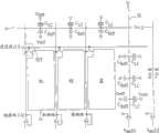
如图1和2中所示,常规液晶显示装置包括彼此相对的第一基板和第二基板(未示出)、填充第一基板与第二基板之间的间隙的液晶层(未示出)、在第一基板上彼此交叉而限定了像素区的选通线11和数据线12,以及形成在选通线11和数据线12的交叉点处的薄膜晶体管(TFT)。第二基板的整个表面上形成有公共电极(未示出,电压(Vcom)),并且第一基板上的像素区上分别形成有像素电极13。As shown in FIGS. 1 and 2, a conventional liquid crystal display device includes a first substrate and a second substrate (not shown) facing each other, a liquid crystal layer (not shown) filling a gap between the first substrate and the second substrate. , a
这里,为了感测电容,在像素区的外部形成有与选通线11平行定位的第一线21和与数据线12平行定位的第二线22,并且进一步形成有分别平行于第一线21和第二线22的第一参考电压线(Vref1)和第二参考电压线(Vref2)。Here, in order to sense capacitance, a first line 21 positioned parallel to the
此外,第一参考电压线(Vref1)与第一线21之间形成有第一辅助电容器(Cref1),并且第一线21与公共电极(Vcom)之间形成有第一液晶电容器(Clc1)。在此情况下,第一辅助电容器(Cref1)和第一液晶电容器(Clc1)串联形成。串联连接的第一辅助电容器(Cref1)和第一液晶电容器(Clc1)分别形成在像素中。Also, a first auxiliary capacitor (Cref1) is formed between the first reference voltage line (Vref1) and the first line 21, and a first liquid crystal capacitor (Clc1) is formed between the first line 21 and the common electrode (Vcom). In this case, the first auxiliary capacitor (Cref1) and the first liquid crystal capacitor (Clc1) are formed in series. A first auxiliary capacitor ( Cref1 ) and a first liquid crystal capacitor ( Clc1 ) connected in series are respectively formed in the pixels.
以相同的方式,第二参考电压线(Vref2)与第二线22之间形成有第二辅助电容器(Cref2),并且公共电极(Vcom)与第二线22之间形成有第二液晶电容器(Clc2)。第二辅助电容器(Cref2)和第二液晶电容器(Clc2)也串联连接。In the same manner, a second auxiliary capacitor (Cref2) is formed between the second reference voltage line (Vref2) and the
这里,在第一线21的末端处设置有放大器31,如图2中所示,因而第一线21感测到的信号获得了从施加到相应辅助电容器(Cref)33与相应液晶电容器(Clc)32之间的每个节点(Vn1)的电压放大了的值,并且通过上面的值来确定装置是否被接触以及接触区域的位置。即,液晶电容器(Clc)32的电压值根据装置是否被接触而变化,并且在通过放大器31从节点(Vn1)输出的电压值不同于液晶电容器(Clc)32的初始电压值的情况下,确定液晶显示装置被接触,并且相应地感测接触区域的位置。Here, an
此外,在辅助电容器(Cref)33与液晶电容器(Clc)32之间与节点(Vn1)的输出侧相对的一侧设置有第一开关和第二开关(sw1和sw2),并且通过第一开关和第二开关(sw1和sw2)选择性地施加信号。Further, a first switch and a second switch ( sw1 and sw2 ) are provided on the side opposite to the output side of the node ( Vn1 ) between the auxiliary capacitor ( Cref ) 33 and the liquid crystal capacitor ( Clc ) 32 , and through the first switch and second switches (sw1 and sw2) selectively apply the signal.
向连接到第一辅助电容器和第二辅助电容器(Cref1和Cref2)33一侧的第一参考电压线和第二参考电压线(Vref1和Vref2)交替地施加两个公共电压值(Vcomh和Vcoml)。当公共电压为值(Vcomh)时,通过第一开关(sw1)施加电压(Va)并且将其存储在液晶电容器(Clc)32中,然后当公共电压为值(Vcoml)时,将电压(Va)输出到放大器31。因此,所输出电压包含液晶电容器(Clc)32的值的数据,该数据在装置被接触时发生变化。输出电压根据电容变化的变化如下。Two common voltage values (Vcomh and Vcoml) are alternately applied to the first and second reference voltage lines (Vref1 and Vref2) connected to the side of the first and second auxiliary capacitors (Cref1 and Cref2) 33 . When the common voltage is the value (Vcomh), the voltage (Va) is applied through the first switch (sw1) and stored in the liquid crystal capacitor (Clc) 32, and then when the common voltage is the value (Vcoml), the voltage (Va ) is output to the
在该构造中,需要设置在X轴和Y轴上的彼此交叉的线,因此可以预料到寄生电容的增大。In this configuration, lines intersecting each other provided on the X-axis and the Y-axis are required, so an increase in parasitic capacitance can be expected.
上面的常规液晶显示装置是以电容方法来识别接触的,它存在如下几个问题。The above conventional liquid crystal display device recognizes contact by a capacitive method, which has the following problems.
首先,选择性地感测与一个像素相对应的点处的电压变化以检测该像素是否被接触,因此当多个点被接触时,无法识别与这些点相对应的几个像素是否被接触。First, a voltage change at a point corresponding to one pixel is selectively sensed to detect whether the pixel is touched, so when multiple points are touched, it is impossible to identify whether several pixels corresponding to the points are touched.
其次,形成彼此交叉的线来感测接触点在X轴和Y轴上的位置以感测接触,可以预料到面板尺寸的增大,线的线电阻和寄生电容由于面板尺寸的增大而增大,并且耦合电容增大由此降低了信噪比(S/N)。因此,信号的稳定性会降低,因此可能难以识别接触。Secondly, forming lines crossing each other to sense the position of the contact point on the X-axis and Y-axis to sense the contact, the increase in the size of the panel can be expected, and the line resistance and parasitic capacitance of the lines increase due to the increase in the size of the panel. Large, and the increase in coupling capacitance thereby reduces the signal-to-noise ratio (S/N). As a result, the stability of the signal will be reduced, so it may be difficult to identify contacts.
发明内容Contents of the invention
因此,本发明旨在提供一种液晶显示装置。Therefore, the present invention aims to provide a liquid crystal display device.
本发明的一个目的是提供一种液晶显示板,其识别由于接触而造成的液晶电容的变化,从而能够感测设备是否被接触以及接触区域的位置。An object of the present invention is to provide a liquid crystal display panel that recognizes a change in liquid crystal capacitance due to a touch, thereby being able to sense whether a device is touched and a position of a touch area.
为了实现该目的和其它优点并且根据这里所体现和广泛描述的本发明的目的,一种液晶显示装置包括:彼此相对的第一基板和第二基板;第一基板上彼此交叉而限定了像素区的多条选通线和多条数据线;分别形成在这多条选通线和多条数据线的交叉点处的像素晶体管,和分别形成在像素区中的像素电极;形成在第二基板的整个表面上的公共电极;填充了第一基板与第二基板之间的间隙的液晶层;像素电极与公共电极之间的液晶电容器;形成在第一基板上的第一存储电极与像素电极之间的第一存储电容器;串联形成在选通线与公共电极之间的第二存储电容器和感测电容器;与数据线平行的读出线;以及多个开关晶体管,每个开关晶体管都设置有连接到第二存储电容器与感测电容器之间的节点上的栅极、连接到读出线的漏极和连接到电源电压线的源极。To achieve this object and other advantages and in accordance with the objects of the present invention embodied and broadly described herein, a liquid crystal display device comprises: a first substrate and a second substrate opposite to each other; the first substrates intersect each other to define pixel regions A plurality of gate lines and a plurality of data lines; pixel transistors respectively formed at intersections of the plurality of gate lines and data lines, and pixel electrodes respectively formed in the pixel regions; formed on the second substrate A common electrode on the entire surface of the substrate; a liquid crystal layer filling a gap between the first substrate and the second substrate; a liquid crystal capacitor between the pixel electrode and the common electrode; a first storage electrode and a pixel electrode formed on the first substrate A first storage capacitor between; a second storage capacitor and a sensing capacitor formed in series between the gate line and the common electrode; a readout line parallel to the data line; and a plurality of switching transistors, each of which is set to There is a gate connected to the node between the second storage capacitor and the sense capacitor, a drain connected to the sense line and a source connected to the supply voltage line.
应该理解,本发明的前述一般描述和以下详细描述都是示例性和说明性的,旨在提供对所要求保护的本发明的进一步说明。It is to be understood that both the foregoing general description and the following detailed description of the present invention are exemplary and explanatory and are intended to provide further explanation of the invention as claimed.
附图说明Description of drawings
附图被包括以提供对本发明的进一步理解,并入本申请而构成其一部分,示出了本发明的实施方式,并且连同说明书一起用于说明本发明的原理。附图中:The accompanying drawings, which are included to provide a further understanding of the invention, and are incorporated in and constitute a part of this application, illustrate embodiments of the invention and together with the description serve to explain the principle of the invention. In the attached picture:
图1是示出以电容方法识别接触的常规液晶显示装置的示意电路图;FIG. 1 is a schematic circuit diagram showing a conventional liquid crystal display device for identifying contacts by a capacitive method;
图2是示出图1的电容传感器及其驱动方法的电路图;2 is a circuit diagram illustrating the capacitive sensor of FIG. 1 and a driving method thereof;
图3是示出根据本发明的液晶显示装置的电路图;3 is a circuit diagram showing a liquid crystal display device according to the present invention;
图4是示出在根据本发明的液晶显示装置中,随着时间流逝,从栅极和节点A看到的电压变化的定时的图;4 is a diagram showing timing of voltage changes seen from the gate and node A as time elapses in the liquid crystal display device according to the present invention;
图5是示出根据本发明的液晶显示装置的平面图;5 is a plan view showing a liquid crystal display device according to the present invention;
图6是沿着图5的线I-I’和II-II’截取的该液晶显示装置的纵向截面图;Fig. 6 is a longitudinal sectional view of the liquid crystal display device taken along lines I-I' and II-II' of Fig. 5;
图7是沿着图5的线III-III’截取的该液晶显示装置的纵向截面图;Fig. 7 is a longitudinal sectional view of the liquid crystal display device taken along line III-III' of Fig. 5;
图8是示出根据本发明另一实施方式的以二极管类型形成的电阻的示意图;而8 is a schematic diagram showing a resistor formed in a diode type according to another embodiment of the present invention; and
图9是示出根据本发明的液晶显示装置中的感测电容器的电容变化所造成的开关晶体管的选通电压变化和漏电流变化的图。FIG. 9 is a graph showing a gate voltage change and a leakage current change of a switching transistor caused by a capacitance change of a sensing capacitor in a liquid crystal display device according to the present invention.
具体实施方式Detailed ways
以下,将参照附图详细描述根据本发明的液晶显示装置及其接触感测方法。Hereinafter, a liquid crystal display device and a touch sensing method thereof according to the present invention will be described in detail with reference to the accompanying drawings.
图3是示出根据本发明的液晶显示装置的电路图。FIG. 3 is a circuit diagram showing a liquid crystal display device according to the present invention.
如图3中所示,本发明的液晶显示装置包括彼此相对以感测接触的第一基板100和第二基板200(参照图4到7)、填充了第一基板与第二基板之间的间隙的液晶层、形成在第一基板100上的薄膜晶体管阵列,和形成在第二基板200上的滤色器阵列。As shown in FIG. 3 , the liquid crystal display device of the present invention includes a
这里,滤色器阵列包括形成在非像素区中的黑底层201(参照图6)、决定相应像素区的颜色的滤色器层202(参照图6),和形成在第二基板200的整个表面上的公共电极203(参照图6)。Here, the color filter array includes a black matrix layer 201 (refer to FIG. 6 ) formed in a non-pixel region, a color filter layer 202 (refer to FIG. 6 ) that determines the color of a corresponding pixel region, and an entire second substrate 200 formed on The
薄膜晶体管阵列包括在第一基板100上彼此交叉(参照图5和6)而限定了像素区的选通线101和数据线102、形成在选通线101与数据线102的交叉点处的像素晶体管(Tpixel)151,以及并联连接在像素晶体管(Tpixel)151的漏端与公共电极203之间的液晶电容器(Clc)152和第一存储电容器(Cst1)153。尽管液晶电容器(Clc)152和第一存储电容器(Cst1)153在电路上并联连接,但是液晶电容器(Clc)152实质上形成在公共电极203、像素晶体管(Tpixel)151的漏端以及在它们之间形成的液晶层之间,而第一存储电容器(Cst1)153实质上形成在像素晶体管(Tpixel)151的漏端与第一电压线(L1)之间。这里,第一电压线L1可单独形成,或者使用公共电极(Cm)或前一选通线(Gn-1)来优化该液晶显示装置的结构。The thin film transistor array includes
此外,在本发明的液晶显示装置中,除了形成在选通线(Gn)101与公共电极203之间的用于驱动像素的像素薄膜晶体管(Tpixel)151以及连接到它的液晶电容器(Clc)152和第一存储电容器(Cst1)153以外,还在选通线(Gn)101与公共电极203之间形成有接触感测单元。Furthermore, in the liquid crystal display device of the present invention, in addition to the pixel thin film transistor (Tpixel) 151 formed between the gate line (Gn) 101 and the
这里,每个接触感测单元都包括:串联连接在选通线(Gn)101与公共电极203之间的第二存储电容器(Cst2)154和感测电容器(Csen)155,以及开关晶体管(Tsw)156,该开关晶体管156配备有连接到第二存储电容器(Cst2)154与感测电容器(Csen)155之间的节点A的栅极、连接到与数据线(Dm)平行铺设的读出线(ROIC)的漏极,以及连接到第二电压线(L2)的源极。每个接触感测单元都还包括形成在节点A与选通线(Gn)101之间的电阻(R1)157,以将电压值稳定地施加到开关晶体管(Tsw)156的栅极。Here, each touch sensing unit includes: a second storage capacitor (Cst2) 154 and a sensing capacitor (Csen) 155 connected in series between the gate line (Gn) 101 and the
接触感测单元可分别形成在像素中,或者以指定数量的像素为间隔而周期性地形成。这里,可考虑接触区域的总面积和像素的总尺寸由位于一个接触区域的面积中的像素数来确定接触感测单元的位置。即,假设位于一个接触区域的面积中的像素数为n,则接触感测单元以n个像素为间隔周期性地形成。The contact sensing units may be respectively formed in pixels, or periodically formed at intervals of a specified number of pixels. Here, the position of the touch sensing unit may be determined by the number of pixels located in the area of one touch area in consideration of the total area of the touch area and the total size of the pixels. That is, assuming that the number of pixels located in the area of one contact region is n, the contact sensing unit is periodically formed at intervals of n pixels.
此外,第一存储电容器(Cst1)153的一侧电极可以是像素电极,而第一存储电容器(Cst1)153的另一侧电极可以是前一选通线(Gn-1)或者按照通过交叠第一电压线(L1)和像素电极而形成的第一存储电容器(Cst1)153的位置,根据选通线在相互平行铺设的像素区中单独形成的公共线106(参照图5)。第二电压线(L2)用于施加电源电压。例如,可使用形成在第一基板100上的公共线(具有图5的线106的形状或单独形成在第一基板100的边缘处的线的形状)作为第二电压线(L2)。In addition, one side electrode of the first storage capacitor ( Cst1 ) 153 may be a pixel electrode, and the other side electrode of the first storage capacitor ( Cst1 ) 153 may be a previous gate line ( Gn-1 ) or by overlapping The position of the first storage capacitor ( Cst1 ) 153 formed by the first voltage line ( L1 ) and the pixel electrode is based on the common line 106 (refer to FIG. 5 ) which is separately formed in the pixel region laid in parallel to each other according to the gate line. The second voltage line (L2) is used to apply a power supply voltage. For example, a common line formed on the first substrate 100 (having the shape of the
读出线(ROIC)用于感测在开关晶体管(Tsw)156中流动的电流,并且在读出线(ROIC)的一端设置了放大器,对感测到的电流进行放大以改善灵敏度。The readout line (ROIC) is used to sense the current flowing in the switching transistor (Tsw) 156, and an amplifier is provided at one end of the readout line (ROIC) to amplify the sensed current to improve sensitivity.
这里,电阻157被配置为具有这样的电阻值(R1),即,使计算出的时间常数(R1·(Csen+Cst2+Csw))小于一帧的时间并且充分大于一个选通高信号的导通时间(1H)。它用于使施加到开关晶体管(Tsw)156的选通电压值维持比施加到开关晶体管(Tsw)156的选通电压信号的导通时间更长的时间,因而当开关晶体管(Tsw)感测接触时,将接触识别稳定地维持至少达开关晶体管(Tsw)156的导通时间。Here, the
这里,Csw表示开关晶体管156的栅极与沟道之间的电容,Cst2表示第二存储电容器154的电容,而Csen表示感测电容器155的电容。Here, Csw represents the capacitance between the gate and the channel of the switching
施加到第二电压线(L2)的第二电压(Vd2)具有不小于常规正电压值的DC电压值,从而当高信号施加到选通线(Gn)101时电流在开关晶体管(Tsw)156中流动。因此,当高信号施加到选通线(Gn)101时,开关晶体管(Tsw)156工作,并且在开关晶体管(Tsw)156中流动的电流被供应到读出线(ROIC)115由此被感测。The second voltage (Vd2) applied to the second voltage line (L2) has a DC voltage value not less than a normal positive voltage value so that current flows in the switching transistor (Tsw) 156 when a high signal is applied to the gate line (Gn) 101 middle flow. Therefore, when a high signal is applied to the gate line (Gn) 101, the switching transistor (Tsw) 156 operates, and the current flowing in the switching transistor (Tsw) 156 is supplied to the readout line (ROIC) 115 thereby being sensed. Measurement.
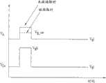
这里,节点A通过电阻157连接到选通线101,因而选通低电压(Vg1)施加到节点A。当第n条选通线导通时,施加到第n条选通线的选通电压从选通低电压(Vg1)变为选通高电压(Vgh),此时,开关晶体管(Tsw)156的选通电压(Vg_sw)如下。Here, the node A is connected to the
图4是示出在根据本发明的液晶显示装置中,随着时间流逝,从栅极和节点A看到的电压变化的定时的图。FIG. 4 is a graph showing the timing of voltage changes seen from the gate and node A as time elapses in the liquid crystal display device according to the present invention.
参照图4,当被接触时,在接触区域处公共电极203与节点A之间的距离减小,因而感测电容器155的电容(Csen)增大且施加到开关晶体管(Tsw)156的选通电压降低。因此,在读出线(ROIC)115中流动的电流减少。Referring to FIG. 4 , when touched, the distance between the
因此,可根据每单位时间在读出线(ROIC)115中流动的电流值来确定设备是否被接触或接触区域的位置。即,如果当前的电流电压相比于被接触之前的初始阶段的电流电压减小,则确定为装置被接触,而如果当前电流电压类似于初始阶段的电流电压,则确定装置未被接触。利用在其上进行感测的选通线和读出线(ROIC)来确定接触区域在X轴和Y轴上的位置。Therefore, whether the device is touched or the position of the contact area can be determined according to the current value flowing in the readout line (ROIC) 115 per unit time. That is, if the current current voltage is lower than that of the initial stage before being touched, it is determined that the device is touched, and if the current current voltage is similar to the current voltage of the initial stage, it is determined that the device is not touched. The position of the contact area on the X-axis and Y-axis is determined using the gate line and the readout line (ROIC) on which the sensing is performed.
下面将参照附图来详细描述根据本发明的带有接触感测单元的液晶显示装置。A liquid crystal display device with a touch sensing unit according to the present invention will be described in detail below with reference to the accompanying drawings.
图5是示出根据本发明的液晶显示装置的平面图,图6是沿着图5的线I-I’和II-II’截取的该液晶显示装置的纵向截面图,而图7是沿着图5的线III-III’截取的该液晶显示装置的纵向截面图。5 is a plan view showing a liquid crystal display device according to the present invention, FIG. 6 is a longitudinal sectional view of the liquid crystal display device taken along lines II' and II-II' of FIG. A longitudinal sectional view of the liquid crystal display device taken along line III-III' of FIG. 5 .
如图5到7中所示,在本发明的液晶显示装置中,彼此交叉而限定了像素区的选通线101和数据线102、形成在像素区中的像素电极103,以及根据选通线101在平行于相应选通线101铺设的像素区的外围部分中形成为U形的公共线106。As shown in FIGS. 5 to 7, in the liquid crystal display device of the present invention, the
这里,每条公共线106都包括:形成在像素区的相应一个的外围部分中的U形图案106a、106b和106c;以及用于将U形图案106a、106b和106c连接到数据线102的相应区域的连接图案。Here, each
像素晶体管(Tpixel)151形成在选通线101与数据线102的交叉点处,并且接触感测单元形成在相同的选通线101与公共电极203之间(第二基板200位于其上),每个接触感测单元都包括第二存储电容器(Cst2)154、感测电容器(Csen)155、电阻(R1)157和开关晶体管(Tsw)156。在图7中,由线III-III’表示的部分示出了第一存储电容器153、像素晶体管151,以及包括第二存储电容器154、感测电容器155、电阻157和开关晶体管156的接触感测单元。A pixel transistor (Tpixel) 151 is formed at the intersection of the
在该实施方式中,如图7中所示,存储电容器(Cst2)154被限定在第一存储图案111a与第一像素电极图案133之间,第一存储图案111a连接到选通线101以具有从选通线101放大的面积,而第一像素电极图案133与第一存储图案111a部分交叠。第一像素电极图案113经由与第一像素电极图案113的下表面相接触的第一数据金属图案112来接收电信号。In this embodiment, as shown in FIG. 7, a storage capacitor (Cst2) 154 is defined between the
如图6和7中所示,感测电容器155具有根据第一像素电极图案133与第二基板200上的公共电极203之间的液晶层的厚度变化而变化的电容值(Csen)。图6示出了在与感测电容器155相对应的位置处另外形成的辅助感测图案210,该辅助感测图案210是可选图案,可被省略。在此情况下,在被接触之前的初始阶段中感测电容器155的电容(Csen)可增大,从而可灵敏地识别被接触时电容的相对变化。As shown in FIGS. 6 and 7 , the
此外,电阻(R1)157包括从第一数据金属图案112延伸的第一电阻连接金属112a、与第一电阻连接金属112a分离的第二电阻连接金属112b,以及分别接触第一和第二电阻连接金属112a和112b的下表面以连接第一和第二电阻连接金属112a和112b的半导体层105。半导体层105是通过堆叠非晶硅层105a和杂质(欧姆接触)层105b而获得的,并且杂质层105b选择性地仅形成在第一和第二电阻连接金属112a和112b与半导体层105之间的接触区域上。In addition, the resistance (R1) 157 includes a first
开关晶体管(Tsw)156包括从平行于数据线102形成的读出线(ROIC)115突出的漏极115a、与漏极115a分离并且形成在与数据线102相同的层中充当源极的第二数据金属图案125,以及形成在漏极115a和第二数据金属图案125下方的层中充当栅极的电极图案111b。The switching transistor (Tsw) 156 includes a
电极图案111b对应于图3的电路图中的节点A,并且电极图案111b与公共线106电接触,因而施加到公共线106上的公共电压信号施加到了电极图案111b上。The
与电极图案111b的上表面部分交叠的电阻157的第一和第二电阻连接金属112a和112b连接到节点A,并且第一电阻连接金属112a电连接到第一数据金属图案112和第一像素电极图案113因而连接到感测电容器(Csen)155和第二存储电容器(Cst2)154中每一个的一个电极上。The first and second
对应于非像素区的黑底层201和对应于像素区的滤色器层202形成在第二基板200上,并且公共电极203形成在包括黑底层201和滤色器层202的第二基板200的整个表面上。可选的是,可进一步在公共电极203的下表面上与接触感测单元的感测电容器(Csen)155相对应的位置处形成辅助感测图案210。The black matrix layer 201 corresponding to the non-pixel area and the color filter layer 202 corresponding to the pixel area are formed on the second substrate 200, and the
此外,还在公共电极203的上表面上设置了对应于黑底层201的上表面的一部分以支持单元间隙(d1)的第一列间隔体220,和对应于黑底层201的上表面的另一部分以具有与第一基板100的上表面的分离距离(d3)的第二列间隔体230。第二列间隔体230与第一基板100的上表面之间的分离距离(d3)是第一和第二基板100和200正常结合时的间隔,并且允许第二列间隔体230和第一基板100的上表面在被施加单独的外部压力时相互接触。即,第二列间隔体230与第一基板100的上表面之间的分离距离(d3)被设为这样的值,即,当所施加的特定外部压力超过指定值时,第二列间隔体230被按下,以便连同第一列间隔体220一起用于展示支持功能。In addition, a
单元间隙(d1)、辅助感测图案210的上表面上的公共电极203与第一像素电极图案113之间的分离距离(d2)、第二列间隔体230与第一基板100的上表面之间的分离距离(d3)满足关系d1>d2>d3。The cell gap (d1), the separation distance (d2) between the
此外,辅助感测图案210的厚度被设置为这样的值,其小于通过从液晶层的单元间隙(d1)中减去第一和第二基板之间的厚度变化(Δd)而获得的值,该厚度变化在接触时改变最大。这样是为了防止在对装置施加压力时,辅助感测图案210上的公共电极203接触第一像素电极图案113(它是感测电容器(Csen)155的一个电极)。In addition, the thickness of the auxiliary sensing pattern 210 is set to a value smaller than a value obtained by subtracting a thickness variation (Δd) between the first and second substrates from the cell gap (d1) of the liquid crystal layer, This thickness change changes most at the time of contact. This is to prevent the
下面将参照图5到7来详细描述制造根据本发明的液晶显示装置的方法。A method of manufacturing a liquid crystal display device according to the present invention will be described in detail below with reference to FIGS. 5 to 7. FIG.
以矩阵形状布置的像素区被限定在第一基板100上,这将在下面进行描述,并且与这些像素区的边界相对应的接触感测单元分别以n个像素区为间隔来形成。Pixel regions arranged in a matrix shape are defined on the
首先,通过在第一基板100上淀积第一金属然后选择性地移除第一金属而形成:布置在一个方向上的选通线101;针对相应的像素区从选通线101突出的栅极101a;在平行于相应选通线101铺设的像素区的外围部分中以U形形成并且彼此连接的、与选通线101分离的公共线106;从与接触感测单元相对应的选通线101突出的第一存储图案111a;以及与第一存储图案111a分离的、配备有电阻形成部分并充当开关晶体管(Tsw)156的栅极的电极图案111b。电极图案111b对应于图3的电路中的节点A。此外,进一步形成邻接开关晶体管(Tsw)156、对应于接触感测单元的下端并且从这些U形公共线106中每一个的一部分突出的公共线突出图案106e。First, by depositing a first metal on the
然后,在包括选通线101、栅极101a、公共线106、第一存储图案111a和电极图案111b的第一基板100的整个表面上形成栅极绝缘膜107。Then, a
然后,通过在栅极绝缘膜107的整个表面上淀积非晶硅层105a和杂质层105b并选择性地将非晶硅层105a和杂质层105b留在栅极101a的与要形成像素晶体管的区域相对应的指定区域上、与开关晶体管(Tsw)的沟道区域相对应的区域上、要形成电阻的区域上,以及像素晶体管的沟道区域上,而形成半导体层105。Then, by depositing the
然后,通过在包括半导体层105的栅极绝缘膜107上淀积第二金属然后选择性地移除第二金属而形成:布置在与选通线101交叉的方向上的数据线102;以及平行于数据线102铺设并且选择性地通过要形成接触感测单元的区域的读出线(ROIC)115。此时,形成了分别从数据线102突出的像素晶体管的源极102a,和分别与这些源极102a分离的像素晶体管的漏极102b。此外,还形成了分别从读出线(ROIC)115突出的开关晶体管(Tsw)的漏极115a,和与漏极115a分离的充当开关晶体管(Tsw)的源极的第二数据金属图案125。此外,还在同一层中形成:第一数据金属图案112,其与接触感测单元的数据线102和读出线(ROIC)105这二者邻接,与第一存储图案11a部分地交叠,并且向下延伸;第一电阻连接金属112a,其连接到第一数据金属图案112并且延伸到要形成每个电阻的区域;以及与第一电阻连接金属112a对称形成的第二电阻连接金属112b。Then, by depositing a second metal on the
形成了充当开关晶体管(Tsw)的源极的第二数据金属图案125以及与第二数据金属图案125分离的开关晶体管(Tsw)的漏极115a后,移除在开关晶体管(Tsw)的源极和漏极之间的区域下方的杂质层105b,因而限定了由堆叠的非晶硅层105a和杂质层105b构成的半导体层136。这里,由于经构图的数据金属,半导体层126和105分别形成在其它区域(要形成电阻和像素晶体管的区域)中。After the second
杂质层105b选择性地仅接触与开关晶体管(Tsw)的源极/漏极125和115a以及像素晶体管(Tpixel)的源极/漏极102a和102b相对应的区域,并且充当欧姆接触层。The
然后,在包括数据线102、读出线(ROIC)115、开关晶体管(Tsw)的源极/漏极125和115a、像素晶体管(Tpixel)的源极/漏极102a和102b、第一和第二数据金属图案112和125,以及第一和第二电阻连接金属112a和112b的第一基板100的整个表面上形成钝化膜108。Then, including the
然后,通过选择性地移除钝化膜108而形成:第一接触孔128,它部分地暴露出像素晶体管(Tpixel)的漏极102b;接触孔129,它部分地暴露出第一存储图案111a上的第一数据金属图案112;第三接触孔130,它暴露出通过部分移除与第二数据金属图案125下方的栅极绝缘膜107和公共线突出图案106e的上表面交叠的第二数据金属图案125而获得的公共线突出图案106e;以及第四接触孔131,它部分地暴露出第一电阻连接金属112a。Then, by selectively removing the
然后,通过在包括第一到第四接触孔128、129、130和131的钝化膜108的整个表面上淀积透明金属然后选择性地移除该透明金属而形成:像素电极103,其填充第一接触孔128并且对应于相应像素区;第一像素电极图案113,其填充第二接触孔129并且与第一数据金属图案112的上表面交叠;第二像素电极123,其填充第三接触孔130并且与公共线突出图案106e交叠;以及第三和第四像素电极图案113a和113b,它们分别与第一电阻连接金属112a和第二电阻连接金属112b交叠。Then, by depositing a transparent metal on the entire surface of the
图8是示出根据本发明另一实施方式的以二极管类型形成的电阻的示意图。FIG. 8 is a schematic diagram illustrating a resistance formed in a diode type according to another embodiment of the present invention.
在图8中,图3的电路图中的电阻(R1)包括薄膜晶体管,该薄膜晶体管的源端和栅端被连接起来而充当二极管。该薄膜晶体管是通过与图5到图7的像素晶体管或开关晶体管的形成方法相同的方法形成的。In FIG. 8, the resistor (R1) in the circuit diagram of FIG. 3 includes a thin film transistor whose source and gate terminals are connected to function as a diode. The thin film transistor is formed by the same method as that of the pixel transistor or the switching transistor of FIGS. 5 to 7 .
图9是示出根据本发明的液晶显示装置中的感测电容器的电容根据开关晶体管的选通电压变化和漏电流变化的变化化的图。FIG. 9 is a graph showing variation of capacitance of a sensing capacitor according to a gate voltage variation and a leakage current variation of a switching transistor in a liquid crystal display device according to the present invention.
图9是示出根据本发明的液晶显示装置中的感测电容器的电容变化(ΔCsen)所造成的开关晶体管的选通电压变化和漏电流变化。FIG. 9 is a graph showing a gate voltage change and a leakage current change of a switching transistor caused by a capacitance change (ΔCsen) of a sensing capacitor in a liquid crystal display device according to the present invention.
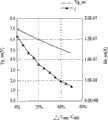
选通电压(Vg_sw)和漏电流(Ids_sw)根据被接触的接触区域的位置处第二基板200上的公共电极203与第一像素电极图案113之间的间隔的减小程度而变化。因而,当接触强度很高时,公共电极203与第一像素电极图案113之间的间隔减小得更多,并且变化值增大。即,当感测电容器的电容增大时,节点A处的选通电压(Vg_sw)降低,如实线所示,并且对应于在开关晶体管的漏端中流动的电流值,如图中穿过三角形点的线条所示。The gate voltage (Vg_sw) and the drain current (Ids_sw) vary according to the degree of reduction of the interval between the
在该图中,Csen表示初始状态(装置未被接触)下感测电容器的电容值。In this figure, Csen represents the capacitance value of the sensing capacitor in the initial state (the device is not touched).
在具有这些接触感测单元的液晶显示装置中,当选择性地导通相应的选通线时,相应接触感测单元的读出线感测到电流。尽管读出线仅设置在数据线的方向上,但是可以通过检测哪条选通线感测到了感测电流来感测接触区域在X轴和Y轴上的位置。In a liquid crystal display device having these contact sensing units, when the corresponding gate lines are selectively turned on, the sense lines of the corresponding contact sensing units sense current. Although the readout lines are arranged only in the direction of the data lines, the positions of the contact areas on the X-axis and Y-axis can be sensed by detecting which gate line has sensed the sensing current.
在接触感测单元中,确定装置是否被接触的标准是设置在液晶显示装置上的元件的寄生电容。例如,在信噪比(S/N)较高的情况下,即使感测电容器的电容变化(ΔCsen)具有10~20%的较低程度,也确定装置被接触,而在信噪比较低的情况下,直到感测电容器的电容变化(ΔCsen)具有20%或更多的较高程度才确定装置被接触。在本发明的液晶显示装置中,优化了接触感测单元和读出线的构造,并且降低了寄生电容因而提高了面板的信噪比。因此,当感测电容器的电容变化(ΔCsen)近似为10~20%时,可以确定装置被接触了。In the touch sensing unit, the criterion for determining whether the device is touched is the parasitic capacitance of elements provided on the liquid crystal display device. For example, in the case of a high signal-to-noise ratio (S/N), it is determined that the device is touched even if the capacitance change (ΔCsen) of the sensing capacitor has a low degree of 10-20%, while in the case of a low signal-to-noise ratio In the case of , it is not determined that the device is touched until the capacitance change (ΔCsen) of the sensing capacitor has a higher degree of 20% or more. In the liquid crystal display device of the present invention, the structure of the touch sensing unit and the readout line is optimized, and the parasitic capacitance is reduced, thereby improving the signal-to-noise ratio of the panel. Therefore, when the capacitance change (ΔCsen) of the sensing capacitor is approximately 10˜20%, it can be determined that the device is touched.
本发明的上述液晶显示装置具有如下效果。The liquid crystal display device of the present invention has the following effects.
首先,与设置有在X轴和Y轴的方向上布置的线(读出线)的常规电容型接触感测液晶显示装置相比,本发明的液晶显示装置设置有在平行于数据线的方向上布置的读出线,因而能够实现结构上的优化并且减少线之间的寄生电容。因此,大面积的液晶显示装置不会受到寄生电容的太多影响,因而能够稳定地感测到接触。First, compared with a conventional capacitive type touch-sensing liquid crystal display device provided with lines (readout lines) arranged in the directions of the X-axis and Y-axis, the liquid crystal display device of the present invention is provided with The readout lines arranged on the top can thus achieve structural optimization and reduce parasitic capacitance between lines. Therefore, a large-area liquid crystal display device will not be greatly affected by parasitic capacitance, and thus can sense touch stably.
其次,不同于受外部光影响的光电型(photo-type)接触感测液晶显示装置,该液晶显示装置借助于接触区域处的电容变化来感测装置是否被接触以及接触区域的位置,因而能够感测到接触而不受外部环境的影响。Secondly, unlike the photo-type touch-sensing liquid crystal display device which is affected by external light, the liquid crystal display device senses whether the device is touched and the position of the contact area by means of the capacitance change at the contact area, thus being able to Touch is sensed regardless of the external environment.
再次,该液晶显示装置包括与液晶板一体形成的接触传感器,用于感测接触而不需附接任何单独的接触板,因而与包括附接到其外表面上的传感器的液晶显示装置相比,能够实现重量轻和外形薄的要求,并且降低了生产成本。Again, the liquid crystal display device includes a touch sensor integrally formed with the liquid crystal panel for sensing contact without attaching any separate touch panel, thus compared with a liquid crystal display device including a sensor attached to its outer surface , can achieve the requirements of light weight and thin profile, and reduce the production cost.
本领域技术人员可以想到的是,可在不偏离本发明的精神或范围的前提下对本发明做出各种修改和变化。因此,本发明旨在涵盖落入所附权利要求及其等同物范围内的本发明的这些修改和变化。It will be apparent to those skilled in the art that various modifications and changes can be made in the present invention without departing from the spirit or scope of the inventions. Thus, it is intended that the present invention covers the modifications and variations of this invention that come within the scope of the appended claims and their equivalents.
本申请要求2008年4月10日提交的韩国专利申请No.2008-033123的优先权,此处通过应用将其并入,就好像在这里进行了充分阐述。This application claims priority from Korean Patent Application No. 2008-033123 filed Apr. 10, 2008, which is hereby incorporated by application as if fully set forth herein.
Claims (10)
Applications Claiming Priority (3)
| Application Number | Priority Date | Filing Date | Title |
|---|---|---|---|
| KR1020080033123 | 2008-04-10 | ||
| KR1020080033123AKR101286538B1 (en) | 2008-04-10 | 2008-04-10 | Liquid crystal display |
| KR10-2008-0033123 | 2008-04-10 |
Publications (2)
| Publication Number | Publication Date |
|---|---|
| CN101556418Atrue CN101556418A (en) | 2009-10-14 |
| CN101556418B CN101556418B (en) | 2011-10-26 |
Family
ID=41163598
Family Applications (1)
| Application Number | Title | Priority Date | Filing Date |
|---|---|---|---|
| CN200810178146XAActiveCN101556418B (en) | 2008-04-10 | 2008-11-24 | Liquid crystal display device |
Country Status (3)
| Country | Link |
|---|---|
| US (1) | US8232974B2 (en) |
| KR (1) | KR101286538B1 (en) |
| CN (1) | CN101556418B (en) |
Cited By (5)
| Publication number | Priority date | Publication date | Assignee | Title |
|---|---|---|---|---|
| CN102778982A (en)* | 2011-05-12 | 2012-11-14 | 宏碁股份有限公司 | Active touch sensing circuit device |
| CN108182901A (en)* | 2018-02-09 | 2018-06-19 | 京东方科技集团股份有限公司 | Display panel and its detection method, display device |
| CN110595648A (en)* | 2019-09-12 | 2019-12-20 | 京东方科技集团股份有限公司 | A kind of pressure sensor and the preparation method of pressure sensor |
| WO2020150984A1 (en)* | 2019-01-25 | 2020-07-30 | 深圳市汇顶科技股份有限公司 | Contact area calculating method and apparatus, touch chip, and electronic device |
| CN112785981A (en)* | 2014-10-29 | 2021-05-11 | 三星显示有限公司 | Display panel, display module and mobile device |
Families Citing this family (19)
| Publication number | Priority date | Publication date | Assignee | Title |
|---|---|---|---|---|
| JP5571298B2 (en)* | 2008-08-07 | 2014-08-13 | 株式会社ジャパンディスプレイ | Liquid crystal display |
| TW201019194A (en)* | 2008-11-07 | 2010-05-16 | Univ Nat Chiao Tung | Multi-sensing method of capacitive touch panel |
| KR101525802B1 (en)* | 2008-12-11 | 2015-06-11 | 삼성디스플레이 주식회사 | Liquid crystal display |
| US8537126B2 (en)* | 2009-04-06 | 2013-09-17 | Apple Inc. | Integrated touch sensitive display gate driver |
| JP2012168571A (en)* | 2009-06-19 | 2012-09-06 | Sharp Corp | Capacitance change detection circuit and display device |
| KR101286550B1 (en) | 2009-09-15 | 2013-07-17 | 엘지디스플레이 주식회사 | Liquid Crystal Display Device |
| CN105702688B (en) | 2009-10-21 | 2020-09-08 | 株式会社半导体能源研究所 | Liquid crystal display device and electronic apparatus including the same |
| KR101290709B1 (en)* | 2009-12-28 | 2013-07-29 | 엘지디스플레이 주식회사 | Touch sensor in-cell type liquid crystal display device and method of fabricating the same |
| TWI435244B (en)* | 2010-06-30 | 2014-04-21 | Au Optronics Corp | Liquid crystal display having touch sensing functionality and touch sensing method thereof |
| WO2012030183A2 (en)* | 2010-09-01 | 2012-03-08 | Lee Sung Ho | Capacitive touch detection apparatus using level shift, detection method using level shift, and display device having the detection apparatus built therein |
| TWI407405B (en)* | 2010-12-10 | 2013-09-01 | Au Optronics Corp | Liquid crystal display having touch sensing functionality and touch sensing method thereof |
| KR101971147B1 (en)* | 2012-04-09 | 2019-04-23 | 삼성디스플레이 주식회사 | Display device including touch sensor |
| KR20140013331A (en)* | 2012-07-23 | 2014-02-05 | 삼성디스플레이 주식회사 | Liquid crystal display device |
| KR102104628B1 (en)* | 2013-08-12 | 2020-04-27 | 삼성디스플레이 주식회사 | Touch screen display device |
| CN103728760A (en)* | 2013-12-26 | 2014-04-16 | 深圳市华星光电技术有限公司 | Touch liquid crystal display and array substrate thereof |
| US9367188B2 (en) | 2014-05-23 | 2016-06-14 | Apple Inc. | RC matching in a touch screen |
| WO2015183334A1 (en)* | 2014-05-28 | 2015-12-03 | Pylemta Management Llc | Narrow border touch screen |
| TWI559185B (en)* | 2014-10-03 | 2016-11-21 | 速博思股份有限公司 | Display device with fingerprint recognition and touch detection |
| TWI581157B (en)* | 2016-04-20 | 2017-05-01 | 群創光電股份有限公司 | Touch display device |
Family Cites Families (7)
| Publication number | Priority date | Publication date | Assignee | Title |
|---|---|---|---|---|
| GB9108226D0 (en)* | 1991-04-17 | 1991-06-05 | Philips Electronic Associated | Optical touch input device |
| US7839392B2 (en)* | 2005-08-05 | 2010-11-23 | Samsung Electronics Co., Ltd. | Sensing circuit and display device having the same |
| KR20070044122A (en)* | 2005-10-24 | 2007-04-27 | 삼성전자주식회사 | Liquid crystal display |
| US20070109239A1 (en)* | 2005-11-14 | 2007-05-17 | Den Boer Willem | Integrated light sensitive liquid crystal display |
| US7573459B2 (en)* | 2006-01-27 | 2009-08-11 | Hannstar Display Corp. | Pixel structure for LCD with embedded touch screen |
| KR101251999B1 (en)* | 2006-06-13 | 2013-04-08 | 삼성디스플레이 주식회사 | Liquid crystal display device, and driving method thereof |
| US8018428B2 (en)* | 2006-11-27 | 2011-09-13 | Samsung Electronics Co., Ltd. | Electrophoretic display panel, electrophoretic display device having the same and method for driving the same |
- 2008
- 2008-04-10KRKR1020080033123Apatent/KR101286538B1/enactiveActive
- 2008-10-30USUS12/261,866patent/US8232974B2/enactiveActive
- 2008-11-24CNCN200810178146XApatent/CN101556418B/enactiveActive
Cited By (9)
| Publication number | Priority date | Publication date | Assignee | Title |
|---|---|---|---|---|
| CN102778982A (en)* | 2011-05-12 | 2012-11-14 | 宏碁股份有限公司 | Active touch sensing circuit device |
| CN102778982B (en)* | 2011-05-12 | 2015-07-08 | 宏碁股份有限公司 | Active touch sensing circuit device |
| CN112785981A (en)* | 2014-10-29 | 2021-05-11 | 三星显示有限公司 | Display panel, display module and mobile device |
| CN112785981B (en)* | 2014-10-29 | 2024-04-12 | 三星显示有限公司 | Display panels, display modules and mobile devices |
| CN108182901A (en)* | 2018-02-09 | 2018-06-19 | 京东方科技集团股份有限公司 | Display panel and its detection method, display device |
| WO2020150984A1 (en)* | 2019-01-25 | 2020-07-30 | 深圳市汇顶科技股份有限公司 | Contact area calculating method and apparatus, touch chip, and electronic device |
| CN111742285A (en)* | 2019-01-25 | 2020-10-02 | 深圳市汇顶科技股份有限公司 | Calculation method, device, touch chip, electronic device for contact area |
| CN110595648A (en)* | 2019-09-12 | 2019-12-20 | 京东方科技集团股份有限公司 | A kind of pressure sensor and the preparation method of pressure sensor |
| CN110595648B (en)* | 2019-09-12 | 2021-03-23 | 京东方科技集团股份有限公司 | Pressure sensor and preparation method thereof |
Also Published As
| Publication number | Publication date |
|---|---|
| US20090256816A1 (en) | 2009-10-15 |
| US8232974B2 (en) | 2012-07-31 |
| CN101556418B (en) | 2011-10-26 |
| KR101286538B1 (en) | 2013-07-16 |
| KR20090107713A (en) | 2009-10-14 |
Similar Documents
| Publication | Publication Date | Title |
|---|---|---|
| CN101556418B (en) | Liquid crystal display device | |
| CN102033348B (en) | Liquid crystal display device | |
| JP5139411B2 (en) | Liquid crystal display device and manufacturing method thereof | |
| US10095335B2 (en) | In-cell type touch panel and manufacturing method thereof, liquid crystal display device | |
| JP3866697B2 (en) | Liquid crystal display device and touch control method thereof | |
| KR101525802B1 (en) | Liquid crystal display | |
| US9557864B2 (en) | Integrated LCD touch screen to determine a touch position based on an induced voltage superimposed on both the scan signal of the gate line and a timing pulse of the signal line | |
| US9007329B2 (en) | Liquid crystal display device including touch panel | |
| US8284169B2 (en) | Display device | |
| TWI402588B (en) | Liquid crystal display including sensing unit | |
| US8300029B2 (en) | Liquid crystal display device and method of manufacturing thereof | |
| US20120105381A1 (en) | Liquid crystal display with integrated touch screen panel | |
| KR20120121705A (en) | In-cell Type Touch Panel | |
| JP2006189868A (en) | Display device and driving method thereof | |
| JP2007503639A (en) | Touch input active matrix display device | |
| JP2013508793A (en) | Liquid crystal device including sensor circuit array using precharge operation | |
| JP2013508792A (en) | Liquid crystal device including a sensor circuit array with a voltage dependent capacitor | |
| CN101620333A (en) | Active matrix display device with touch control function | |
| CN107656643B (en) | Display panel and electronic equipment | |
| KR101451579B1 (en) | Liquid crystal display | |
| KR20060105248A (en) | Display | |
| KR20070050208A (en) | Display Device and Thin Film Transistor Display Panel |
Legal Events
| Date | Code | Title | Description |
|---|---|---|---|
| C06 | Publication | ||
| PB01 | Publication | ||
| C10 | Entry into substantive examination | ||
| SE01 | Entry into force of request for substantive examination | ||
| C14 | Grant of patent or utility model | ||
| GR01 | Patent grant |