CN101553956B - Multiple-antenna device having an isolation element - Google Patents
Multiple-antenna device having an isolation elementDownload PDFInfo
- Publication number
- CN101553956B CN101553956BCN2007800453090ACN200780045309ACN101553956BCN 101553956 BCN101553956 BCN 101553956BCN 2007800453090 ACN2007800453090 ACN 2007800453090ACN 200780045309 ACN200780045309 ACN 200780045309ACN 101553956 BCN101553956 BCN 101553956B
- Authority
- CN
- China
- Prior art keywords
- antenna
- circuit board
- transceiver
- printed circuit
- conductive support
- Prior art date
- Legal status (The legal status is an assumption and is not a legal conclusion. Google has not performed a legal analysis and makes no representation as to the accuracy of the status listed.)
- Expired - Fee Related
Links
- 238000002955isolationMethods0.000titleclaimsabstractdescription102
- 238000007493shaping processMethods0.000claimsdescription50
- 230000010287polarizationEffects0.000claimsdescription33
- 230000005672electromagnetic fieldEffects0.000claims4
- WIDHRBRBACOVOY-UHFFFAOYSA-N2,3,4,3',4'-PentachlorobiphenylChemical compoundC1=C(Cl)C(Cl)=CC=C1C1=CC=C(Cl)C(Cl)=C1ClWIDHRBRBACOVOY-UHFFFAOYSA-N0.000description17
- 239000002184metalSubstances0.000description11
- 230000001413cellular effectEffects0.000description6
- 238000004891communicationMethods0.000description6
- 238000010586diagramMethods0.000description6
- 230000008901benefitEffects0.000description5
- 238000000034methodMethods0.000description4
- 238000000926separation methodMethods0.000description4
- 230000005540biological transmissionEffects0.000description3
- 238000004519manufacturing processMethods0.000description3
- 230000004048modificationEffects0.000description3
- 238000012986modificationMethods0.000description3
- 230000005855radiationEffects0.000description3
- 230000000694effectsEffects0.000description2
- 230000006870functionEffects0.000description2
- 238000012544monitoring processMethods0.000description2
- 239000012811non-conductive materialSubstances0.000description2
- 238000004806packaging method and processMethods0.000description2
- 230000008569processEffects0.000description2
- 239000007787solidSubstances0.000description2
- 238000003491arrayMethods0.000description1
- 238000005452bendingMethods0.000description1
- 230000008878couplingEffects0.000description1
- 238000010168coupling processMethods0.000description1
- 238000005859coupling reactionMethods0.000description1
- 238000013461designMethods0.000description1
- 238000007865dilutingMethods0.000description1
- 238000005516engineering processMethods0.000description1
- 238000005562fadingMethods0.000description1
- 230000006872improvementEffects0.000description1
- 230000003993interactionEffects0.000description1
- 230000002452interceptive effectEffects0.000description1
- 238000013519translationMethods0.000description1
Images


Classifications
- H—ELECTRICITY
- H01—ELECTRIC ELEMENTS
- H01Q—ANTENNAS, i.e. RADIO AERIALS
- H01Q21/00—Antenna arrays or systems
- H—ELECTRICITY
- H01—ELECTRIC ELEMENTS
- H01Q—ANTENNAS, i.e. RADIO AERIALS
- H01Q9/00—Electrically-short antennas having dimensions not more than twice the operating wavelength and consisting of conductive active radiating elements
- H01Q9/04—Resonant antennas
- H01Q9/0407—Substantially flat resonant element parallel to ground plane, e.g. patch antenna
- H—ELECTRICITY
- H01—ELECTRIC ELEMENTS
- H01Q—ANTENNAS, i.e. RADIO AERIALS
- H01Q1/00—Details of, or arrangements associated with, antennas
- H01Q1/007—Details of, or arrangements associated with, antennas specially adapted for indoor communication
- H—ELECTRICITY
- H01—ELECTRIC ELEMENTS
- H01Q—ANTENNAS, i.e. RADIO AERIALS
- H01Q1/00—Details of, or arrangements associated with, antennas
- H01Q1/12—Supports; Mounting means
- H01Q1/22—Supports; Mounting means by structural association with other equipment or articles
- H01Q1/24—Supports; Mounting means by structural association with other equipment or articles with receiving set
- H—ELECTRICITY
- H01—ELECTRIC ELEMENTS
- H01Q—ANTENNAS, i.e. RADIO AERIALS
- H01Q1/00—Details of, or arrangements associated with, antennas
- H01Q1/36—Structural form of radiating elements, e.g. cone, spiral, umbrella; Particular materials used therewith
- H01Q1/38—Structural form of radiating elements, e.g. cone, spiral, umbrella; Particular materials used therewith formed by a conductive layer on an insulating support
- H—ELECTRICITY
- H01—ELECTRIC ELEMENTS
- H01Q—ANTENNAS, i.e. RADIO AERIALS
- H01Q1/00—Details of, or arrangements associated with, antennas
- H01Q1/52—Means for reducing coupling between antennas; Means for reducing coupling between an antenna and another structure
- H01Q1/521—Means for reducing coupling between antennas; Means for reducing coupling between an antenna and another structure reducing the coupling between adjacent antennas
- H—ELECTRICITY
- H01—ELECTRIC ELEMENTS
- H01Q—ANTENNAS, i.e. RADIO AERIALS
- H01Q1/00—Details of, or arrangements associated with, antennas
- H01Q1/52—Means for reducing coupling between antennas; Means for reducing coupling between an antenna and another structure
- H01Q1/526—Electromagnetic shields
- H—ELECTRICITY
- H01—ELECTRIC ELEMENTS
- H01Q—ANTENNAS, i.e. RADIO AERIALS
- H01Q15/00—Devices for reflection, refraction, diffraction or polarisation of waves radiated from an antenna, e.g. quasi-optical devices
- H01Q15/24—Polarising devices; Polarisation filters
- H—ELECTRICITY
- H01—ELECTRIC ELEMENTS
- H01Q—ANTENNAS, i.e. RADIO AERIALS
- H01Q19/00—Combinations of primary active antenna elements and units with secondary devices, e.g. with quasi-optical devices, for giving the antenna a desired directional characteristic
- H01Q19/10—Combinations of primary active antenna elements and units with secondary devices, e.g. with quasi-optical devices, for giving the antenna a desired directional characteristic using reflecting surfaces
- H—ELECTRICITY
- H01—ELECTRIC ELEMENTS
- H01Q—ANTENNAS, i.e. RADIO AERIALS
- H01Q21/00—Antenna arrays or systems
- H01Q21/06—Arrays of individually energised antenna units similarly polarised and spaced apart
- H01Q21/08—Arrays of individually energised antenna units similarly polarised and spaced apart the units being spaced along or adjacent to a rectilinear path
- H—ELECTRICITY
- H01—ELECTRIC ELEMENTS
- H01Q—ANTENNAS, i.e. RADIO AERIALS
- H01Q21/00—Antenna arrays or systems
- H01Q21/24—Combinations of antenna units polarised in different directions for transmitting or receiving circularly and elliptically polarised waves or waves linearly polarised in any direction
- H—ELECTRICITY
- H01—ELECTRIC ELEMENTS
- H01Q—ANTENNAS, i.e. RADIO AERIALS
- H01Q25/00—Antennas or antenna systems providing at least two radiating patterns
- H01Q25/005—Antennas or antenna systems providing at least two radiating patterns providing two patterns of opposite direction; back to back antennas
- H—ELECTRICITY
- H01—ELECTRIC ELEMENTS
- H01Q—ANTENNAS, i.e. RADIO AERIALS
- H01Q5/00—Arrangements for simultaneous operation of antennas on two or more different wavebands, e.g. dual-band or multi-band arrangements
- H—ELECTRICITY
- H01—ELECTRIC ELEMENTS
- H01Q—ANTENNAS, i.e. RADIO AERIALS
- H01Q5/00—Arrangements for simultaneous operation of antennas on two or more different wavebands, e.g. dual-band or multi-band arrangements
- H01Q5/50—Feeding or matching arrangements for broad-band or multi-band operation
Landscapes
- Physics & Mathematics (AREA)
- Electromagnetism (AREA)
- Transceivers (AREA)
- Variable-Direction Aerials And Aerial Arrays (AREA)
- Support Of Aerials (AREA)
- Details Of Aerials (AREA)
- Radio Transmission System (AREA)
Abstract
Translated fromChinese
Description
Translated fromChinese相关申请的交叉引用Cross References to Related Applications
本发明涉及并要求2006年12月11日提交的题为“METRO WIFI RFREPEATER(城域WIFI RF中继器)”的美国临时专利申请No.60/869,438的优先权,该申请的内容通过援引纳入于此。This application is related to and claims priority to U.S. Provisional Patent Application No. 60/869,438, entitled "METRO WIFI RF REPEATER," filed December 11, 2006, the contents of which are incorporated by reference here.
技术领域technical field
本发明一般涉及无线通信,尤其涉及与无线中继器相关联的天线配置,该天线配置是由具有正交偏振和隔离以降低电磁耦合并提供高方向性的紧密封装天线构成的。The present invention relates generally to wireless communications, and more particularly to antenna configurations associated with wireless repeaters consisting of closely packed antennas with orthogonal polarizations and isolation to reduce electromagnetic coupling and provide high directivity.
发明背景Background of the invention
在诸如设计成与能够同时发射和接收分组(即,双工操作)的无线系统一起操作的无线中继器等无线通信节点中,天线单元的定向在建立非干扰操作时可能是重要的,因为发射信号不使接收机的灵敏度降低是关键所在。这可包括使用时分双工(TDD)、频分双工(FDD)或其他合需双工操作方法的网络。In wireless communication nodes such as wireless repeaters designed to operate with wireless systems capable of transmitting and receiving packets simultaneously (i.e., duplex operation), the orientation of the antenna elements can be important in establishing non-interfering operation because The key is to transmit the signal without desensitizing the receiver. This may include networks using time division duplex (TDD), frequency division duplex (FDD), or other desired duplex methods of operation.
此外,将天线模块和中继器电路封入相同的封装内对于便利性、制造成本降低等而言是合需的,但是这种封装会导致干扰问题。Furthermore, enclosing the antenna module and repeater circuitry within the same package is desirable for convenience, reduced manufacturing costs, etc., but such packaging can lead to interference problems.
在全双工中继器封装中,一个天线或天线集可与例如基站等一起操作,而另一天线可与订户一起操作。由于相同或不同频率的多个信号将在靠在一起的天线中被发射和接收,因此这些天线的隔离变得很重要,这在中继器的两侧执行同时发射和接收之时尤其重要。In a full-duplex repeater package, one antenna or set of antennas can operate with, for example, a base station, while the other antenna can operate with a subscriber. Since multiple signals of the same or different frequencies will be transmitted and received in close together antennas, the isolation of these antennas becomes important, especially when both sides of the repeater are performing simultaneous transmission and reception.
此外,由于中继器单元将所有电路纳入单个封装之内,因此期望在最小天线-天线交互作用的情况下靠近地定位天线,同时保持可接受的增益且在多数情形中保持可接受的方向性。Furthermore, since the repeater unit incorporates all circuitry within a single package, it is desirable to position the antennas closely with minimal antenna-to-antenna interaction while maintaining acceptable gain and in most cases acceptable directivity .
为了易于制造,示例性中继器应当被配置成使其可易于使用低成本封装在大批量制造过程中生产。示例性中继器应当易于设置以助益便利的客户操作。然而,在紧邻地封装中继器天线和电路时,会产生其他问题。首先,天线之间单单因物理紧邻度就难以达成高隔离,即使在使用定向天线的情况下也是如此。For ease of manufacture, the exemplary repeater should be configured such that it can be easily produced in a high-volume manufacturing process using low-cost packaging. Exemplary repeaters should be easy to set up to facilitate convenient customer operation. However, other problems arise when the repeater antenna and circuitry are packaged in close proximity. First, the physical proximity of antennas alone makes it difficult to achieve high isolation, even when directional antennas are used.
简言之,随着天线愈被放置成靠在一起,天线彼此间就愈可能耦合能量,这降低了中继器两侧之间的隔离。由于被放置成彼此靠近的天线的交迭辐射方向图往往产生干扰效应,因此维持全向或半全向天线方向图变得困难。来自天线的能量可能通过电路元件——诸如通过共享接地平面——被进一步电耦合,在其中多个天线被集成且接地平面很小的配置中尤其如此。虽然使用定向天线会使中继器在增大的射程和减小的无线信号变动——其归因于瑞利衰落效应——的方面获益,但是定向天线通常由于超出普通用户的能力或期望的对方向性对准的要求而未被用于室内应用。In short, as the antennas are placed closer together, the antennas are more likely to couple energy to each other, which reduces the isolation between the two sides of the repeater. Maintaining omnidirectional or semi-omnidirectional antenna patterns becomes difficult as overlapping radiation patterns of antennas placed close to each other tend to create interference effects. Energy from the antennas may be further electrically coupled through circuit elements, such as through a shared ground plane, especially in configurations where multiple antennas are integrated and the ground plane is small. While the use of directional antennas would benefit repeaters in terms of increased range and reduced wireless signal variation due to the Rayleigh fading effect, directional antennas are often The requirement for directional alignment has not been used for indoor applications.
一些改进可通过抵消或类似技术来获得,其中在中继器的另一侧上出现相同信号的情况下,在中继器一侧发射的信号的版本被用于移除该相同信号。然而,这种抵消是昂贵的,因为需要附加电路,并且可能是计算量庞大的,因为这种抵消会导致在中继器中引入延迟因子,或者另外可能要求使用更昂贵和更迅速的处理器来执行抵消功能。Some improvement may be obtained by cancellation or similar techniques, where a version of the signal transmitted on one side of the repeater is used to remove the same signal if it is present on the other side of the repeater. However, this cancellation is expensive as additional circuitry is required, and may be computationally intensive as it introduces a delay factor in the repeater, or may otherwise require the use of more expensive and faster processors to perform the offsetting function.
发明内容Contents of the invention
本发明通过提供一种以印刷电路板形式形成的多天线设备来克服以上问题。该设备包括:第一天线,形成于印刷电路板的第一侧上;第二天线,形成于印刷电路板的第二侧上;接地平面,形成于第一天线与第二天线之间,该接地平面被配置成提供第一天线与第二天线之间的电磁隔离;第一非导电支承部件,形成于第一天线与接地平面之间;第二非导电支承部件,形成于第二天线与接地平面之间。第一天线被电连接到印刷电路板上的第一馈送点,该第一馈送点未被连接到接地平面,并且第二天线被电连接到印刷电路板上的第二馈送点,该第二馈送点未被连接到接地平面。The present invention overcomes the above problems by providing a multi-antenna device formed in the form of a printed circuit board. The device includes: a first antenna formed on a first side of a printed circuit board; a second antenna formed on a second side of the printed circuit board; a ground plane formed between the first antenna and the second antenna, the a ground plane configured to provide electromagnetic isolation between the first antenna and the second antenna; a first non-conductive support member formed between the first antenna and the ground plane; a second non-conductive support member formed between the second antenna and the ground plane between ground planes. The first antenna is electrically connected to a first feed point on the printed circuit board, which is not connected to the ground plane, and the second antenna is electrically connected to a second feed point on the printed circuit board, the second The feed point is not connected to the ground plane.
还提供了一种多天线设备,该设备包括:印刷电路板,其具有配置成提供印刷电路板的第一侧与印刷电路板的第二侧之间的电磁隔离的接地平面;第一非导电支承部件,形成于印刷电路板的第一侧之上;第二非导电支承部件,形成于印刷电路板的第二侧之上;第三非导电支承部件,形成于印刷电路板的第二侧之上;第四非导电支承部件,形成于印刷电路板的第一侧之上;第一天线,形成于第一非导电支承部件之上;第二天线,形成于第二非导电支承部件之上;第三天线,形成于第三非导电支承部件之上;以及第四天线,形成于第四非导电支承部件之上。There is also provided a multi-antenna device comprising: a printed circuit board having a ground plane configured to provide electromagnetic isolation between a first side of the printed circuit board and a second side of the printed circuit board; a first non-conductive A support member formed on the first side of the printed circuit board; a second non-conductive support member formed on the second side of the printed circuit board; a third non-conductive support member formed on the second side of the printed circuit board above; the fourth non-conductive support member is formed on the first side of the printed circuit board; the first antenna is formed on the first non-conductive support member; the second antenna is formed on the second non-conductive support member on; a third antenna formed on the third non-conductive support member; and a fourth antenna formed on the fourth non-conductive support member.
还提供了一种以印刷电路板形式形成的多天线设备,该设备包括:第一天线,形成于印刷电路板的第一侧上;第二天线,形成于印刷电路板的第二侧上;接地平面,形成于第一天线与第二天线之间,该接地平面被配置成提供第一天线与第二天线之间的电磁隔离;第一非导电支承部件,形成于第一天线与接地平面之间;第二非导电支承部件,形成于第二天线与接地平面之间。第一天线被电连接到印刷电路板上的第一馈送点,该第一馈送点未被连接到接地平面,并且第二天线被电连接到印刷电路板上的第二馈送点,该第二馈送点未被连接到接地平面。There is also provided a multi-antenna device formed in the form of a printed circuit board, the device comprising: a first antenna formed on a first side of the printed circuit board; a second antenna formed on a second side of the printed circuit board; a ground plane formed between the first antenna and the second antenna, the ground plane configured to provide electromagnetic isolation between the first antenna and the second antenna; a first non-conductive support member formed between the first antenna and the ground plane between; the second non-conductive support member is formed between the second antenna and the ground plane. The first antenna is electrically connected to a first feed point on the printed circuit board, which is not connected to the ground plane, and the second antenna is electrically connected to a second feed point on the printed circuit board, the second The feed point is not connected to the ground plane.
附图简述Brief description of the drawings
各个附图用于进一步图解各实施例以及说明根据本发明的各原理和优点,这些附图中相同的附图标记贯穿各个视图指代相同或功能上类似的元件并连同以下详细描述一起结合到说明书中且构成其一部分。The various drawings serve to further illustrate the various embodiments and illustrate principles and advantages in accordance with the invention, like reference numerals in the drawings designate the same or functionally similar elements throughout the various views and are incorporated together with the following detailed description Instructions and constitutes a part thereof.
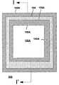
图1是根据各个示例性实施例的双天线、多收发机设备的侧视图。FIG. 1 is a side view of a dual-antenna, multi-transceiver device in accordance with various exemplary embodiments.
图2是根据各个示例性实施例的图1的双天线、多收发机设备的俯视图。2 is a top view of the dual-antenna, multi-transceiver device of FIG. 1 in accordance with various exemplary embodiments.
图3是根据各个示例性实施例的图1的双天线、多收发机设备的仰视图。3 is a bottom view of the dual-antenna, multi-transceiver device of FIG. 1 in accordance with various exemplary embodiments.
图4是根据各个示例性实施例的四天线、多收发机设备的侧视图。4 is a side view of a four-antenna, multi-transceiver device in accordance with various exemplary embodiments.
图5是根据各个示例性实施例的图4的四天线、多收发机设备的俯视图。5 is a top view of the four-antenna, multi-transceiver device of FIG. 4 in accordance with various exemplary embodiments.
图6是根据各个示例性实施例的图4的四天线、多收发机设备的仰视图。6 is a bottom view of the four-antenna, multi-transceiver device of FIG. 4 in accordance with various exemplary embodiments.
图7是根据各个示例性实施例的图4的四天线、多收发机设备的上侧的说明性视图。7 is an illustrative view of the upper side of the four-antenna, multi-transceiver device of FIG. 4, in accordance with various exemplary embodiments.
图8是根据各个示例性实施例的图4的四天线、多收发机设备的框图。8 is a block diagram of the four-antenna, multi-transceiver device of FIG. 4, in accordance with various exemplary embodiments.
图9是根据各个示例性实施例的包括图4的四天线、多收发机设备的网络的框图。9 is a block diagram of a network including the four-antenna, multi-transceiver device of FIG. 4, according to various exemplary embodiments.
图10是根据各个示例性实施例的配置成在多个频带上工作的四天线、多收发机设备的框图。10 is a block diagram of a four-antenna, multi-transceiver device configured to operate on multiple frequency bands in accordance with various exemplary embodiments.
详细描述A detailed description
提供本公开以进一步以可实现方式说明执行本发明的一个或多个实施例的最佳模式。还提供本公开以增进对本发明原理及其优点的理解和领会,而非以任何方式限制本发明。本发明仅由所附权利要求——包括在本申请待批期间作出的任何修改以及所授权的这些权利要求的所有等效方案——来定义。This disclosure is provided to further illustrate, in an achievable manner, the best mode of carrying out one or more embodiments of the invention. This disclosure is also provided to enhance an understanding and appreciation of the principles of the invention and its advantages, but not to limit the invention in any way. The invention is defined solely by the appended claims including any amendments made during the pendency of this application and all equivalents of those claims as issued.
还应当理解,诸如第一和第二等关系术语(若有)的使用仅被用于将实体、项目、或动作彼此区分开,而不一定要求或暗示这些实体、项目或动作之间的任何实际的此类关系或次序。注意:一些实施例可包括可按任何次序执行的多个过程或步骤,除非明确且必要地限于特定次序;即,非如此受限的过程或步骤可按任何次序执行。It should also be understood that the use of relational terms, such as first and second, if any, are used only to distinguish entities, items, or actions from each other and do not necessarily require or imply any relationship between these entities, items, or actions. actual such relationship or sequence. NOTE: Some embodiments may include multiple processes or steps that may be performed in any order, unless explicitly and necessarily limited to a specific order; ie, processes or steps that are not so limited may be performed in any order.
众多本发明的功能以及众多本发明的原理在实现之时,得到软件或集成电路(IC)——诸如由此的数字信号处理器或软件或专用IC——或在其中得到很好的支持。尽管可能付出了相当努力以及存在由诸如可用时间、当前技术和经济考虑等促成的众多设计抉择,但是预期本领域技术人员在本文所公开的概念和原理的指导之下将能够在最小限度的实验下轻而易举生成此类软件指令或IC。因此,为了简化或最小化任何淡化根据本发明的原理和概念的风险,此类软件或IC(若有)的进一步的讨论将限于与示例性实施例所用的原理和概念相关的本质。Many of the inventive functions and many of the inventive principles are implemented with or well supported in software or integrated circuits (ICs), such as digital signal processors or software or dedicated ICs thereby. While considerable effort may have been expended and numerous design choices driven by, for example, available time, current technology, and economic considerations, it is expected that those skilled in the art will be able to, with minimal experimentation, be guided by the concepts and principles disclosed herein. Generating such software instructions or ICs is a snap. Therefore, in order to simplify or minimize any risk of diluting the principles and concepts in accordance with the present invention, further discussion of such software or ICs (if any) will be limited to those essential to the principles and concepts employed by the exemplary embodiments.
申请人在以下参照附图,其中类似附图标记指代类似组件,且其中单个附图标记可被用于标识多个类似组件的示例性之一。Applicants hereinafter refer to the drawings in which like reference numerals refer to like components and in which a single reference numeral may be used to identify an exemplary one of a plurality of similar components.
双天线多收发机设备Dual-antenna multi-transceiver equipment
图1是根据各个示例性实施例的双天线、多收发机设备的侧视图。图2是图1的双天线、多收发机设备的俯视图,而图3是图1的双天线、多收发机设备的仰视图。FIG. 1 is a side view of a dual-antenna, multi-transceiver device in accordance with various exemplary embodiments. FIG. 2 is a top view of the dual-antenna, multiple-transceiver device of FIG. 1 , and FIG. 3 is a bottom view of the dual-antenna, multiple-transceiver device of FIG. 1 .
如图1-3中所示的,设备100包括:印刷电路板(PCB)105,其包括接地平面110并且具有第一侧200和第二侧300;第一收发机电路120A和第二收发机电路120B;第一电磁隔离元件125A和第二电磁隔离元件125B;第一天线130A和第二天线130B;第一非导电支承部件135A和第二非导电支承部件135B;第一水平连接元件140A和第二水平连接元件140B;第一垂直连接元件150A和第二垂直连接元件150B;以及第一场成形元件160A和第二场成形元件160B。第一收发机电路120A和第二收发机电路120B通过连接元件170电连接,该连接元件170穿过接地平面110但是未被连接到接地平面110。As shown in FIGS. 1-3, the device 100 includes: a printed circuit board (PCB) 105 including a
PCB 105提供用于附连电路的结构并且可提供各种电路元件之间的连接线。其包括接地平面110,后者可用作连接至PCB 105的任何元件的统一接地电势。接地平面110还被设计成使其将从第一侧200上的第一天线130A辐射的EM场与从第二侧300上的第二天线130B辐射的EM场隔离开。PCB 105 provides a structure for attaching circuitry and may provide connection lines between various circuit elements. It includes a
PCB 105的第一侧200具有形成于其上的第一收发机电路120A、第一电磁隔离元件125A、第一天线130A、第一非导电支承部件135A、和第一场成形元件160A。第一收发机电路120A直接形成于PCB 105上;第一电磁隔离元件125A形成为覆盖第一收发机电路120A,以使其电隔离;第一非导电支承部件135A形成于第一电磁隔离元件125A上,且第一天线130A形成于第一非导电支承部件135A上。第一天线130A经由第一水平连接元件140A和第一垂直连接元件150A连接到第一收发机电路120A,该第一水平连接元件140A和第一垂直连接元件150A穿过第一电磁隔离元件125A但是不与之电连接。第一场成形元件160A被形成为围绕第一天线130A。The
PCB 105的第二侧300具有形成于其上的第二收发机电路120B、第二电磁隔离元件125A、第二天线130B、第二非导电支承部件135B、和第二场成形元件160B。第二收发机电路120B直接形成于PCB 105上;第二电磁隔离元件125B形成为覆盖第二收发机电路120B,以使其电隔离;第二非导电支承部件135B形成于第二电磁隔离元件125B上,且第二天线130B形成于第二非导电支承部件135B上。第二天线130B经由第二水平连接元件140B和第二垂直连接元件150B连接到第二收发机电路120B,该第二水平连接元件140B和第二垂直连接元件150B穿过第二电磁隔离元件125B但是不与之电连接。第二场成形元件160B被形成为围绕第二天线130B。The
第一收发机电路120A和第二收发机电路120B各自包括使用第一天线130A和第二天线130B来发送和接收信号的一个或多个收发机。此类收发机的工作细节应为本领域普通技术人员所理解的,因此将不再赘述。如果设置了一个以上的收发机,则可以各种方式布置这多个收发机以使得它们可与一些或所有其他收发机通信以及与天线130A和130B中的一者或两者通信。The
尽管所公开的实施例公开了第一收发机电路120A和第二收发机电路120B,但是在不要求全收发机的实施例中,这些电路中的任一者或两者可用专用发射机或接收机电路来替代。Although the disclosed embodiments disclose a
在图1-3的实施例中,设置了两个收发机电路120A和120B——在PCB 105的每一侧上各一个,并且两者通过连接元件170电连接。通常如此进行以达成PCB 105上有限空间的高效利用,并且还可能抵消掉跨PCB 105的电信号。然而,替换性实施例可仅使用在PCB 105的单侧上形成的单个收发机电路。在此情形中,两个天线130A和130B将被连接到单个收发机电路。In the embodiment of FIGS. 1-3, two
另外,尽管图1-3的实施例公开了收发机电路120A和120B被形成于PCB105上且分别在天线130A和130B之下,但是这仅仅是作为示例。在替换性实施例中,收发机电路(分成多个电路或聚集在一起)可远离PCB 105形成。在这样的情形中,非导电支承部件135A和135B将直接形成于PCB 105上,且天线130A和130B分别形成于非导电支承部件135A和135B上。天线130A和130B可在随后被电连接到PCB 105上的电线,这些电线随后被连接到外部收发机电路。Additionally, although the embodiment of FIGS. 1-3 discloses that
第一电磁隔离元件125A位于设备100的第一侧200上,并且在第一收发机电路120A之上。其用于在第一收发机电路120A之间进行电磁隔离。类似地,第二电磁隔离元件125B位于设备100的第二侧300上,并且在第二收发机电路120B之上。其用于将第二收发机电路120B和第二天线130B电磁隔离。第一电磁隔离元件125A和第二电磁隔离元件125B用于使收发机电路120A和120B的操作所导致的EM辐射将干扰相应侧上的天线的可能性最小化。The first
在一些实施例中,PCB 105可以是多层PCB,并且收发机电路120A和120B中的一者或两者将形成于PCB 105中。在此情形中,第一电磁隔离元件125A和第二电磁隔离元件125B可以是PCB 105中的附加接地平面。在其他实施例中,第一电磁隔离元件125A和第二电磁隔离元件125B可以是套在相应收发机电路120A和120B上的金属外壳,或者可以是任何其他适于提供EM隔离的合适设备。无论如何,第一电磁隔离元件125A和第二电磁隔离元件125B应当各自被连接至接地平面110以使它们保持与接地平面110相同的电势。In some embodiments,
在一些实施例中,第一电磁隔离元件125A和第二电磁隔离元件125B可被配置成提供第一天线130A与第二天线130B之间的附加隔离。然而,在其他实施例中,第一电磁隔离元件125A和第二电磁隔离元件125B可被配置成主要向收发机电路120A和120B提供隔离。In some embodiments, the first
第一天线130A和第二天线130B是配置成发射来自收发机电路110的EM信号或为其接收EM信号的EM天线。在一些实施例中,第一天线130A和第二天线130B可以是形成于PCB上或靠近其形成的平面天线,诸如片状天线或缝隙天线。然而,可被恰当隔离的任何合适的天线可被用在替换实施例中,例如,偶极子天线、“倒F”天线等。The
在图1-3的实施例中,天线130A和130B被配置成使其可发射彼此正交的信号以进一步降低这些信号之间的干扰。出于公开的简洁起见,它们将被描述为在水平定向和同该水平定向正交的垂直定向上发射信号。然而,应当理解,这些代表任何彼此正交的定向,不管其相对于诸如局部地面等任何基准平面的定向如何。例如,“水平”定向可与地面成45°,而“垂直”定向可与地面成135°。其他定向显然是可能的。In the embodiment of FIGS. 1-3,
第一非导电支承部件135A和第二非导电支承部件135B由非导电材料形成,且用于将天线130A和130B与第一电磁隔离元件125A和第二电磁隔离元件125B隔开。根据需要,它们可以是实心或空心的。可选择第一非导电支承部件135A和第二非导电支承部件135B的尺寸和布置以便为天线130A和130B设置特定发射和接收参数,因为天线130A和130B与第一电磁隔离元件125A和第二电磁隔离元件125B之间的分隔会影响天线130A和130B的场参数。The first
第一水平连接元件140A和第二水平连接元件140B将第一天线130A和第二天线130B的相应之一的水平边缘连接到收发机电路120A和120B的相应之一,以使得信号可在水平定向上被发射或接收。The first horizontal connecting
第一垂直连接元件150A和第二垂直连接元件150B将第一天线130A和第二天线130B的相应之一的垂直边缘连接到收发机电路120A和120B的相应之一,以使得信号可在垂直定向上被发射或接收。The first
由于这些连接元件140A、140B、150A和150B形成90°的分隔,因此它们形成正交偏振,这也可被用在各种配置中以改进两个天线振子之间的隔离。它们还可被用于设备100中无线电信号的分集接收。Since these connecting
在一些实施例中,可省去第一水平连接元件140A和第二水平连接元件140B、以及第一垂直连接元件150A和第二垂直连接元件150B中的一个或多个。例如,如果第一天线130A仅在垂直定向上发射和接收信号,且第二天线130B仅在水平定向上发射和接收信号,则第一垂直连接元件150A和第二水平连接元件140B可被省去。In some embodiments, one or more of the first
在使用不同类型天线的替换实施例中,可用使天线在给定定向上发射信号的相应元件来替代第一水平连接元件140A和第二水平连接元件140B、以及第一垂直连接元件150A和第二垂直连接元件150B。In an alternate embodiment using a different type of antenna, the first horizontal connecting
第一场成形元件160A和第二场成形元件160B是在相应的第一天线130A和第二天线130B的边缘周围形成的金属结构,以使从天线结构的一侧辐射的场(即,信号)成形,从而使得这些场中到达相反侧上的天线的部分被极大的减少或消去。场成形元件160A和160B应当经由成形连接元件165连接到接地平面110,以使得场成形元件160A和160B处在与接地平面110相同的电势。The first field-shaping
场成形元件160A和160B可以是PCB的边缘上伸出的金属栅栏,或者可以是环绕PCB边缘的实际金属环。还可通过在PCB的边缘上设置锯齿形或其他图案来形成场成形元件160A和160B,以减小边缘衍射以及接地平面边缘。在一些实施例中,场成形元件160A和160B也可被用作散热片。
在其中通过使用接地平面110和电磁隔离元件125A和125B以及正交天线就能提供充分隔离的一些实施例中,可省去第一场成形元件160A和第二场成形元件160B。一些实施例还可在设备100的一侧设置一个或多个场成形元件,但另一侧上不设置。In some embodiments where sufficient isolation can be provided by using
在一些实施例中,场成形元件160A和160B可由金属薄片制成,且形成为带有弹簧指,以使得在设备封装的盖子与PCB组装时,这些弹簧指朝着至少一个接地平面被压紧,以使得将来自天线一侧的EM场相对于相反侧上的场隔离开。这些结构还可通过沟槽或夹具被附连到盖子以使得能够易于将其组装到盖子中。In some embodiments, the
四天线多收发机设备Four-antenna multi-transceiver device
尽管双天线设备是具有电磁隔离元件的多天线设备的最简单的示例,但是可使用更多数目个天线。图4-10描述了使用四个天线——每侧两个——的实施例。Although a two-antenna device is the simplest example of a multi-antenna device with electromagnetic isolation elements, a greater number of antennas may be used. Figures 4-10 describe an embodiment using four antennas - two on each side.
图4是根据各个示例性实施例的四天线、多收发机设备的侧视图。图5是图4的四天线、多收发机设备的俯视图,而图6是图4的四天线、多收发机设备的仰视图。4 is a side view of a four-antenna, multi-transceiver device in accordance with various exemplary embodiments. 5 is a top view of the four-antenna, multiple-transceiver device of FIG. 4, and FIG. 6 is a bottom view of the four-antenna, multiple-transceiver device of FIG.
如图4-6中所示的,设备400包括:印刷电路板(PCB)405——其包括接地平面410并且具有第一侧500和第二侧600,第一收发机电路420A和第二收发机电路420B、第一电磁隔离元件425A和第二电磁隔离元件425B、第一天线430A、第二天线430B、第三天线430C和第四天线430D、第一非导电支承部件435A、第二非导电支承部件435B、第三非导电支承部件435C和第四非导电支承部件435D、第一水平连接元件440A、第二水平连接元件440B、第三水平连接元件440C和第四水平连接元件440D、第一垂直连接元件450A、第二垂直连接元件450B、第三垂直连接元件450C和第四垂直连接元件450D、以及第一场成形元件460A、第二场成形元件460B、第三场成形元件460C和第四场成形元件460D。第一收发机电路420A和第二收发机电路420B通过连接元件470电连接,该连接元件470穿过接地平面410但是未被连接到接地平面410。As shown in FIGS. 4-6, the
PCB 405提供用于附连电路的结构并且可提供各种电路元件之间的连接线。其包括接地平面410,后者可用作连接至PCB 405的任何元件的统一接地电势。接地平面410还被设计成使其将从第一侧500上的第一天线430A和第四天线430D辐射的EM场与从第二侧600上的第二天线430B和第三天线430C辐射的EM场隔离开。
PCB 405的第一侧500具有形成于其上的第一收发机电路420A、第一电磁隔离元件425A、第一天线430A和第四天线430D、第一非导电支承部件435A和第四非导电支承部件435D、以及第一场成形元件460A和第四场成形元件460D。第一收发机电路420A直接形成于PCB 405上;第一电磁隔离元件425A形成为覆盖第一收发机电路420A,以使其电隔离;第一非导电支承部件435A和第四非导电支承部件435D形成于第一电磁隔离元件425A上,且第一天线430A和第四天线430D分别形成于第一非导电支承部件435A和第四非导电支承部件435D上。第一天线430A和第四天线430D经由第一水平连接元件440A和第四水平连接元件440D以及第一垂直连接元件450A和第四垂直连接元件450D分别连接到第一收发机电路420A,该第一水平连接元件440A和第四水平连接元件440D以及第一垂直连接元件450A和第四垂直连接元件450D穿过第一电磁隔离元件425A但是不与之电连接。第一场成形元件460A和第四场成形元件460D分别形成于第一天线430A和第四天线430D的边缘上。The
PCB 405的第二侧600具有形成于其上的第二收发机电路420B、第二电磁隔离元件425B、第二天线430B和第三天线430C、第二非导电支承部件435B和第三非导电支承部件435C、以及第二场成形元件460B和第三场成形元件460C。第二收发机电路420B直接形成于PCB 405上;第二电磁隔离元件425B形成为覆盖第二收发机电路420B,以使其电隔离;第二非导电支承部件435B和第三非导电支承部件435C形成于第二电磁隔离元件425B上,且第二天线430B和第三天线430C分别形成于第二非导电支承部件435B和第三非导电支承部件435C上。第一天线430B和第四天线430C经由第二水平连接元件440A和第三水平连接元件440D以及第二垂直连接元件450B和第三垂直连接元件450C分别连接到第二收发机电路420B,该第二水平连接元件440A和第三水平连接元件440D以及第二垂直连接元件450B和第三垂直连接元件450C穿过第二电磁隔离元件425B但是不与之电连接。第二场成形元件460B和第三场成形元件460C分别形成于第二天线430B和第三天线430C的边缘上。The
第一收发机电路420A和第二收发机电路420B各自包括使用第一到第四天线430A-430D中的至少之一来发送和接收信号的一个或多个收发机。此类收发机的工作细节应为本领域普通技术人员所理解的,因此将不再赘述。如果设置了一个以上的收发机,则可以各种方式布置这多个收发机以使得它们可与一些或所有其他收发机通信以及与天线430A-430D中的一者或全部通信。The
尽管所公开的实施例公开了第一收发机电路420A和第二收发机电路420B,但是在不要求全收发机的实施例中,这些电路中的任一者或两者可用专用发射机或接收机电路来替代。Although the disclosed embodiments disclose a
在图4-6的实施例中,设置了两个收发机电路420A和420B——在PCB 405的每一侧上各一个,并且两者通过连接元件470电连接。通常如此进行以达成PCB 405上有限空间的高效利用,并且还可能抵消掉跨PCB 405的电信号。然而,替换性实施例可仅使用在PCB 405的单侧上形成的单个收发机电路。在此情形中,所有天线430A-430B将被连接到单个收发机电路。In the embodiment of FIGS. 4-6, two
另外,尽管图4-6的实施例公开了收发机电路420A和1420B被形成于PCB405上且分别在天线430A-430D之下,但是这仅仅是作为示例。在替换性实施例中,收发机电路(分成多个电路或聚集在一起)可远离PCB 405形成。在这样的情形中,非导电支承部件435A-435D将直接形成于PCB 405上,且天线430A-430D分别形成于非导电支承部件435A-435D上。天线430A-430D可在随后被电连接到PCB 405上的电线,这些电线随后被连接到外部收发机电路。Additionally, while the embodiment of FIGS. 4-6 discloses that
第一隔离元件425A位于设备400的第一侧500上,并且在第一收发机电路420A之上。其用于电磁隔离第一收发机电路420A。类似地,第二电磁隔离元件425B位于设备400的第二侧600上,并且在第二收发机电路420B之上。其用于提供第二收发机电路420B同第二天线430B和第三天线430C之间的电磁(EM)隔离。第一电磁隔离元件425A和第二电磁隔离元件425B用于使收发机电路420A和420B的操作所导致的EM辐射将干扰相应侧上的天线的可能性最小化。The
在一些实施例中,PCB 405可以是多层PCB,并且收发机电路420A和420B中的一者或两者将形成于PCB 405中。在此情形中,第一电磁隔离元件425A和第二电磁隔离元件425B可以是PCB 405中的附加接地平面。在其他实施例中,第一电磁隔离元件425A和第二电磁隔离元件425B可以是套在相应收发机电路420A和420B上的金属外壳,或者可以是任何其他适于提供EM隔离的合适设备。无论如何,第一电磁隔离元件425A和第二电磁隔离元件425B应当各自被连接至接地平面410以使它们保持与接地平面410相同的电势。In some embodiments,
在一些实施例中,第一电磁隔离元件425A和第二电磁隔离元件425B可被配置成提供第一天线430A和第四天线430D与第二天线430B和第三天线430C之间的附加隔离。然而,在其他实施例中,第一电磁隔离元件425A和第二电磁隔离元件425B可被配置成主要向收发机电路420A和420B提供隔离。In some embodiments, the first
第一到第四天线430A-430D是配置成发射来自收发机电路420A和420B的EM信号或为其接收EM信号的EM天线。在一些实施例中,第一到第四天线430A-430D可以是形成于PCB上或靠近其形成的平面天线,诸如片状天线或缝隙天线。然而,可被恰当隔离的任何合适的天线可被用在替换实施例中,例如,偶极子天线、“倒F”天线等。The first through
在图4-6的实施例中,天线430A-430D被配置成使其可发射与其他天线430A-430D中的一个或多个正交的信号以进一步降低这些信号之间的干扰。出于公开的简洁起见,它们将被描述为在水平定向和同该水平定向正交的垂直定向上发射信号。然而,应当理解,这些代表任何彼此正交的定向,不管其相对于诸如局部地面等任何基准平面的定向如何。例如,“水平”定向可与地面成45°,而“垂直”定向可与地面成135°。其他定向显然是可能的。In the embodiment of FIGS. 4-6,
第一到第四非导电支承部件435A-435D由非导电材料形成,且用于将天线430A-430D与第一电磁隔离元件425A和第二电磁隔离元件425B隔开。根据需要,它们可以是实心或空心的。可选择第一到第四非导电支承部件435A-435D的尺寸和布置以便为天线430A-430D设置特定发射和接收参数,因为天线430A-430D与第一电磁隔离元件425A和第二电磁隔离元件425B之间的分隔会影响天线430A-430D的场参数。The first to fourth
第一到第四水平连接元件440A-440D将第一到第四天线430A-430D的相应之一的水平边缘连接到收发机电路420A和420B的相应之一,以使得信号可在水平定向上被发射或接收。The first to fourth
第一到第四垂直连接元件450A-440D将第一到第四天线430A-430D的相应之一的垂直边缘连接到收发机电路420A和420B的相应之一,以使得信号可在垂直定向上被发射或接收。First to fourth
由于这些连接元件440A-440D和450A-450D形成90°的分隔,因此它们形成正交偏振,这也可被用在各种配置中以改进两个天线振子之间的隔离。它们还可被用于设备400中无线电信号的分集接收。Since these connecting
对天线定向的确切选择可逐实施例不同,并且甚至可在设备400的工作中变动。例如,第一天线430A和第二天线430B可使用水平定向工作,而第三天线430C和第四天线430D可使用垂直定向工作。这样,可向给定侧上的两个天线(第一侧500上的第一天线430A和第四天线430D,以及第二侧600上的第二天线430B和第三天线430C)提供一些隔离,而不用考虑它们之间没有电磁隔离元件这个事实。在替换性方案中,第一天线430A和第四天线430D可使用水平定向工作,而第二天线430B和第三天线430C可使用垂直定向工作。根据需要,还可使用其他可能的定向排列中的任一者。The exact choice of antenna orientation may vary from embodiment to embodiment, and may even vary during operation of
由于这些实施例中的天线430A-430D各自具有垂直馈送和水平馈送两者,因此它们可被按需选择成在垂直或水平方向上发射。Since the
然而,在一些实施例中,可省去第一到第四水平连接元件440A-440D、以及第一到第四垂直连接元件450A-450D中的一个或多个。例如,如果第一天线430A和第二天线430B仅在垂直定向上发射和接收信号,且第三天线430C和第四天线430D仅在水平定向上发射和接收信号,则可省去第一水平连接元件440A和第二水平连接元件440B、以及第三垂直连接元件450C和第四垂直连接元件450D。如本领域普通技术人员将理解的,各种其他排列也是可能的。However, in some embodiments, one or more of the first through fourth
在使用不同类型天线的替换实施例中,可用使天线在给定定向上发射信号的相应元件来替代第一到第四水平连接元件440A-440D、以及第一到第四垂直连接元件450A-450D。In an alternate embodiment using a different type of antenna, the first through fourth horizontal connecting
第一到第四场成形元件460A-460D是在相应的第一到第四天线430A-430D的边缘周围形成的金属结构,以使从天线结构的一侧辐射的场(即,信号)成形,从而使得这些场中到达相反侧上的天线的部分被极大的减少或消去。这些场成形元件460A-460D应当经由成形连接元件465连接到接地平面410,以使得场成形元件460A-460D处在与接地平面110相同的电势。The first to fourth
场成形元件460A-460D可以是PCB的边缘上伸出的金属栅栏,或者可以是环绕PCB边缘的实际金属环。还可通过在PCB的边缘上设置锯齿形或其他图案来形成场成形元件160A和160B,以减小边缘衍射以及接地平面边缘。在一些实施例中,场成形元件460A-460D也可被用作散热片。The
在其中通过使用接地平面410和电磁隔离元件425A和425B以及正交天线就能提供充分隔离的一些实施例中,可省去场成形元件460A-460D中的一些或全部。一些实施例还可在设备400的一侧设置一个或多个场成形元件,但另一侧上不设置。In some embodiments where sufficient isolation can be provided through the use of
在一些实施例中,场成形元件460A-460D可由金属薄片制成,且形成为带有弹簧指,以使得在设备封装的盖子与PCB组装时,这些弹簧指朝着至少一个接地平面被压紧,以使得将来自天线一侧的EM场相对于相反侧上的场隔离开。这些结构还可通过沟槽或夹具被附连到盖子以使得能够易于将其组装到盖子中。In some embodiments, the
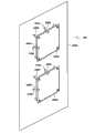
图7是根据各个示例性实施例的图4的四天线、多收发机设备的上侧的说明性视图。如图7中所示的,设备400的第一侧500作为示例被示出。所公开的实施例中的第一侧500包括第一天线430A和第四天线430D。7 is an illustrative view of the upper side of the four-antenna, multi-transceiver device of FIG. 4, in accordance with various exemplary embodiments. As shown in Figure 7, the
这些实施例中的第一天线430A和第四天线430D是由大小被适当调节以辐射感兴趣的期望频率的金属平板构成。通过下弯突出的金属指状物并将其附连到相应馈送点770A、770D、775A和775D——这些馈送点最终被连接到收发机电路420A或420B之一——来将第一垂直连接元件450A和第四垂直连接元件450D以及第一水平连接元件440A和第二水平连接元件440D集成到相应的天线430A和430D。在其中电磁隔离元件425A是形成于收发机电路420A上的物理电磁干扰(EMI)屏蔽的实施例中,馈送点770A、770D、775A和775D穿过电磁隔离元件425A以连接到收发机电路420A。The
如图7中所示的,非导电支承部件435A和435D是在安装在相应天线430A和430D之下并且通过多个接线柱被连接到电磁隔离元件125A的方形元件。As shown in FIG. 7,
图8是根据各个示例性实施例的图4的四天线、多收发机设备的框图。如图8中所示的,设备400包括具有第一天线430A和第四天线430D的第一侧500、具有第二天线430B和第三天线430C的第二侧600、以及包括多收发机电路870和控制器880的屏蔽的多收发机元件850。8 is a block diagram of the four-antenna, multi-transceiver device of FIG. 4, in accordance with various exemplary embodiments. As shown in FIG. 8, the
以上关于图5和图6详细描述了第一侧500和第二侧600。在图8中所公开的实施例中,第一到第四天线430A-430D全部是双向的。在不同的工作模式中,它们可被用作发射/接收阵列,并且按照需要一些进行发射而一些进行接收。在替换实施例中,按照需要,特定天线可以是专用发射或接收天线。The
多收发机电路870包括PCB 405以及第一收发机电路420A和第二收发机电路420B。其包含接收来自天线430A-430D的信号以及向天线430A-430D发射信号所需的所有电路。这可包括放大器、滤波器、上变频器和下变频器、交换机、频率变换电路、分组调制器和解调器、信号检测器、自动增益控制电路等。如以上所述的,收发机的一般操作在本领域中是公知的,且在此不进行详细描述。The
控制器880包括控制多收发机电路870的操作所需的电路。这可包括用户接口、信道监视电路、分组监视电路和存储器元件。此类控制器的一般操作在本领域中是公知的,且在此不进行详细描述。The
四天线双收发机设备的操作Operation of a four-antenna dual-transceiver device
图9是根据各个示例性实施例的包括图4的四天线、多收发机设备的网络900的框图。如图9中所示的,网络900包括在基站910与订户920之间通信的多天线、多收发机设备400。FIG. 9 is a block diagram of a
多天线、多收发机设备400包括具有第一天线430A和第四天线430D的第一侧500、具有第二天线430B和第三天线430C的第二侧600、以及屏蔽的多收发机元件850。这些元件在以上进行了更详细的描述。The multi-antenna,
第一网络910和第二网络920代表需要在彼此之间传递信息的无线网络。各个实施例可在不同的第一网络910和第二网络920之间进行连接。在一个实施例中,第一网络910可以是蜂窝电话网,而第二网络920可以是诸如IEEE802.11网络的局域网(LAN)。在另一实施例中,第一网络910可以是蜂窝电话网,而第二网络920可以是个人通信服务(PCB)网络。然而,其他实施例可能对应需要被连接的任何网络集合。The
将关于第一网络910向第二网络920传递下行链路信号930和935、以及第二网络920向第一网络910传递上行链路信号940和945来描述此网络的操作。然而,这仅作为示例。通信链路930、935、940和945可以是任何合需信号集合。The operation of this network will be described with respect to the
当第二网络920需要向第一网络910发送上行链路消息时,其在由设备400的第二侧600上的第三天线430C接收的上行链路信号940中传送上行链路消息。第三天线430C将上行链路消息传递通过屏蔽的多收发机元件850(即,经过任何电磁隔离元件),并从设备400的第一侧500上的第四天线430D在上行链路信号945中传送上行链路消息。上行链路信号945随后被第一网络910接收。When the
类似地,当第一网络910需要向第二网络930发送下行链路消息时,其在由设备400的第一侧500上的第一天线430A接收的下行链路信号930中传送下行链路消息。第一天线430A将下行链路消息传递通过屏蔽的多收发机元件850(即,经过任何电磁隔离元件),并从设备400的第二侧600上的第二天线430B在下行链路信号935中传送下行链路消息。下行链路信号935随后被第二网络920接收。Similarly, when the
然而,由于电磁隔离元件或场成形元件将第一侧500上的信号(即,下行链路信号930和上行链路信号945)与第二侧6000上的信号(即,下行链路信号935和上行链路信号940)隔离开,因此两个信号集之间的干扰可得以最小化,即使用于发送和接收这两类信号的收发机形成于同一PCB上也是如此。However, since the electromagnetic isolation element or field shaping element separates the signal on the first side 500 (i.e., the
另外,设备400的第一侧500上的上行链路信号945和下行链路信号930也可通过诸如频分复用、时分复用、信道分割复用、正交传输等手段来隔离。类似地,设备400的第二侧600上的上行链路信号940和下行链路信号935也可通过类似手段来隔离。In addition, the
这一些状况中,第一网络910与第二网络920之间可能有简易的物理划分。例如,在一个实施例中,第一网络910可以是蜂窝网络,而第二网络920可以是家庭LAN。这种情况在运行LAN的订户具有对以某类订阅为基础的蜂窝网络的接入权限时是可能出现的。In some cases, there may be a simple physical division between the
在此情形中,在订户的住宅内,第二网络920(即,LAN)很可能是最强的。在订户的住宅之外,第一网络910(即,蜂窝网络)很可能是最强的。多天线设备400可由此被放置在住宅的窗户上或靠近其放置,以便利用这个事实。具体而言,设备400的第一侧500可面向窗户(即,面向蜂窝网络)放置,而设备400的第二侧600可面向住宅的内部(即,面向LAN)放置。In this case, within the subscriber's residence, the second network 920 (ie, LAN) is likely to be strongest. Outside the subscriber's residence, the first network 910 (ie, the cellular network) is likely to be strongest. The
这在其中两个网络的物理划分显著的任意境况中同样有效。This is equally valid in any situation where the physical division of the two networks is significant.
尽管在以上的公开中第一天线430A和第三天线430C被示为操作成接收机天线,且第二天线430B和第四天线430D被示为操作成发射机天线,但是这仅作为示例。这些天线430A-430D可全部皆为双向天线,且其操作可按需要改变成发送或发射信号。Although in the above disclosure the
使用多频带的操作Operation using multiple bands
图10是根据各个示例性实施例的配置成在多频带中操作的四天线、多收发机设备1000的框图。此设备1000可使用可用天线的可变配置来自由地跨两个不同频带发射信号。10 is a block diagram of a four-antenna,
如图10中所示的,设备1000包括具有第一侧1040和第二侧1080的屏蔽的多收发机元件1001。屏蔽的多收发机元件1001包括第一频带收发机1002和1004、第一频带基带电路1006、第二频带收发机1012和1014、第二频带基带电路1016、双工器1022、1024、1026、1028、1062、1064、1066和1068、共用器1030、1035、1070和1075;第一侧1040包括天线1045A和1045B;以及第二侧1080包括天线1085A和1085B。尽管未在图10中示出,但是设备1000包括如上所描述的至少一个电磁隔离元件,从而提供第一侧1040上的天线1045A和1045B、以及第二侧1080上的天线1085A和1085B之间的电磁(EM)隔离。As shown in FIG. 10 ,
天线1045A可发送或接收信号1050;天线1045B可发送或接收信号1055;天线1085A可发送或接收信号1090;以及天线1085B可发送或接收信号1095。这些天线1045A、1045B、1085A和1085B可以是平面(例如,片状)天线,或者任何其他可彼此有效地隔离的合意天线类型。
第一频带收发机1002通过双工器1022、1024、1026和1028以及共用器1030和1035连接到天线1045A和1045B以经由天线1045A和1045B发送或接收数据。第一频带收发机1004通过双工器1062、1064、1066和1068以及共用器1070和1075连接到天线1085A和1085B以经由天线1085A和1085B发送或接收数据。第一频带基带电路1006被连接到第一频带收发机1002与第一频带收发机1004之间以提供这两个电路之间的通信。The
第二频带收发机1012通过双工器1022、1024、1026和1028以及共用器1030和1035连接到天线1045A和1045B以经由天线1045A和1045B发送或接收数据。第二频带收发机1014通过双工器1062、1064、1066和1068以及共用器1070和1075连接到天线1085A和1085B以经由天线1085A和1085B发送或接收数据。第二频带基带电路1016被连接到第二频带收发机1012与第二频带收发机1014之间以提供这两个电路之间的通信。The
共用器1030、1035被连接到天线1045A和1045B与双工器1022、1024、1026和1028之间。它们操作用于确定哪些信号将在天线1045A和1045B与第一频带收发机1002之间、以及在天线1045A和1045B与第二频带收发机1012之间传递。
共用器1030、1035被配置成基于频率将信号分开,从而向/从双工器1022和1024传递第一频带的信号,以及向/从双工器1024和1028传递第二频带的信号。
双工器1022、1024被连接到共用器1030、1035与第一频带收发机1002之间;而双工器1026、1028被连接到共用器1030、1035与第二频带收发机1012之间。这些双工器1022、1024、1026、1028用于分别路由第一或第二频带内频率略微不同的信号,以在第一频带收发机1002和第二频带收发机1012与共用器1030、1035之间恰当地指引所发射或接收的信号。The
共用器1070、1075被连接到天线1085A和1085B与双工器1062、1064、1066和1068之间。它们操作用于确定哪些信号将在天线1085A和1085B与第一频带收发机1004之间、以及在天线1085A和1085B与第二频带收发机1014之间传递。
共用器1070、1075被配置成基于频率将信号分开,从而向/从双工器1062和1064传递第二频带的信号,以及向/从双工器1064和1068传递第一频带的信号。
双工器1062、1064被连接到共用器1070、1075与第二频带收发机1014之间;而双工器1066、1068被连接到共用器1070、1075与第一频带收发机1004之间。这些双工器1062、1064、1066、1068用于分别路由第一或第二频带内频率略微不同的信号,以在第一频带收发机1004和第二频带收发机1014与共用器1070、1075之间恰当地指引所发射或接收的信号。The
在替换实施例中,可省去双工器1022、1024、1026、1028、1062、1064、1066、1068、1070和1075或共用器1030、1035、1070和1075中的一些,因为在一些实施例中,特定频带和天线的排列可能被禁用。In alternative embodiments, some of
在其他实施例中,来自不同频带的信号可被专门指派至特定发射定向。在此类实施例中,双工器1022、1024、1026、1028、1062、1064、1066和1068的输出可被直接连接到天线1045A、1045B、1085A和1085B。例如,第一频带可被指定始终使用水平定向发射/接收,而第二频带可被指定始终使用垂直定向发射/接收。在这样的实施例中,双工器1022可被直接连接到天线1045A的水平导线;双工器1024可被直接连接到天线1045B的水平导线;双工器1026可被直接连接到天线1045A的垂直导线;双工器1028可被直接连接到天线1045B的垂直导线;双工器1062可被直接连接到天线1085A的垂直导线;双工器1064可被直接连接到天线1085B的垂直导线;双工器1066可被直接连接到天线1085A的水平导线;以及双工器1068可被直接连接到天线1085B的水平导线。In other embodiments, signals from different frequency bands may be specifically assigned to particular transmission directions. In such embodiments, the outputs of
尽管以上实施例示出了仅使用两个或四个天线连同两个收发机,但是这仅作为示例。使用不同数目个天线或收发机的多天线、多收发机设备也可被使用。Although the above embodiments show the use of only two or four antennas along with two transceivers, this is by way of example only. Multiple antenna, multiple transceiver devices using different numbers of antennas or transceivers may also be used.
此外,尽管以上实施例皆显示天线与PCB分开,但是替换实施例可将天线直接形成于PCB的相反侧上。在此类实施例中,PCB内的绝缘层可形成所需的非导电支承部件以将天线与接地平面隔开。而且,在此类实施例中,收发机很可能形成于PCB之外,并且可通过PCB上的布线连接到天线。此类集成结构可提供更紧凑的设备。Additionally, although the above embodiments all show the antenna being separate from the PCB, alternative embodiments may form the antenna directly on the opposite side of the PCB. In such embodiments, an insulating layer within the PCB may form the non-conductive support required to separate the antenna from the ground plane. Also, in such embodiments, the transceiver is likely to be formed off the PCB, and can be connected to the antenna via traces on the PCB. Such an integrated structure can provide a more compact device.
结论in conclusion
本公开意在说明如何制作和使用根据本发明的各个实施例,而无意限制其真实预期且明确的范围和精神。在前描述并非旨在穷举或将本发明限于所公开的精确形式。鉴于以上教义,修改或变化是可能的。选择并描述各实施例是为了提供对本发明的原理及其实践应用的最佳例示,且为了使本领域技术人员能够按各个实施例利用本发明以及在作出适于具体预期使用的各个修改之下利用本发明。所有此类修改和变化皆落在由所附权利要求——其在本专利申请的待批期间可被修改、及其所有等效方案所确定的范围内,只要是根据其被正当、合法且公正授予的广度内来解释即可。以上所描述的各个电路可按实现的需要在分立电路或集成电路中实现。This disclosure is intended to illustrate how to make and use various embodiments according to the invention, not to limit the scope and spirit of which it is truly intended and expressed. The foregoing description is not intended to be exhaustive or to limit the invention to the precise forms disclosed. Modifications or variations are possible in light of the above teachings. The embodiments were chosen and described in order to provide the best illustration of the principles of the invention and its practical application, and to enable others skilled in the art to utilize the invention in each embodiment and with each modification as is suited to the particular contemplated use. Take advantage of the present invention. All such modifications and variations are within the scope determined by the appended claims, as may be amended during the pendency of this patent application, and all equivalents thereof, provided they are fairly, legally and It can be interpreted within the breadth of justice granted. The various circuits described above can be implemented in discrete circuits or integrated circuits according to the needs of implementation.
Claims (17)
Translated fromChineseApplications Claiming Priority (3)
| Application Number | Priority Date | Filing Date | Title |
|---|---|---|---|
| US86943806P | 2006-12-11 | 2006-12-11 | |
| US60/869,438 | 2006-12-11 | ||
| PCT/US2007/025234WO2008073372A2 (en) | 2006-12-11 | 2007-12-11 | Multiple-antenna device having an isolation element |
Publications (2)
| Publication Number | Publication Date |
|---|---|
| CN101553956A CN101553956A (en) | 2009-10-07 |
| CN101553956Btrue CN101553956B (en) | 2013-03-27 |
Family
ID=39512296
Family Applications (1)
| Application Number | Title | Priority Date | Filing Date |
|---|---|---|---|
| CN2007800453090AExpired - Fee RelatedCN101553956B (en) | 2006-12-11 | 2007-12-11 | Multiple-antenna device having an isolation element |
Country Status (9)
| Country | Link |
|---|---|
| US (2) | US7592969B2 (en) |
| EP (1) | EP2122761A4 (en) |
| JP (1) | JP2010512713A (en) |
| KR (1) | KR101123595B1 (en) |
| CN (1) | CN101553956B (en) |
| BR (1) | BRPI0720168A2 (en) |
| CA (1) | CA2670535C (en) |
| RU (1) | RU2399125C1 (en) |
| WO (1) | WO2008073372A2 (en) |
Families Citing this family (70)
| Publication number | Priority date | Publication date | Assignee | Title |
|---|---|---|---|---|
| US9215754B2 (en) | 2007-03-07 | 2015-12-15 | Menu Networks | Wi-Fi virtual port uplink medium access control |
| US9185618B1 (en) | 2005-12-05 | 2015-11-10 | Meru Networks | Seamless roaming in wireless networks |
| US9142873B1 (en) | 2005-12-05 | 2015-09-22 | Meru Networks | Wireless communication antennae for concurrent communication in an access point |
| US9794801B1 (en) | 2005-12-05 | 2017-10-17 | Fortinet, Inc. | Multicast and unicast messages in a virtual cell communication system |
| US9730125B2 (en) | 2005-12-05 | 2017-08-08 | Fortinet, Inc. | Aggregated beacons for per station control of multiple stations across multiple access points in a wireless communication network |
| US9215745B1 (en) | 2005-12-09 | 2015-12-15 | Meru Networks | Network-based control of stations in a wireless communication network |
| US9025581B2 (en) | 2005-12-05 | 2015-05-05 | Meru Networks | Hybrid virtual cell and virtual port wireless network architecture |
| US8160664B1 (en) | 2005-12-05 | 2012-04-17 | Meru Networks | Omni-directional antenna supporting simultaneous transmission and reception of multiple radios with narrow frequency separation |
| US8064601B1 (en) | 2006-03-31 | 2011-11-22 | Meru Networks | Security in wireless communication systems |
| US8472359B2 (en) | 2009-12-09 | 2013-06-25 | Meru Networks | Seamless mobility in wireless networks |
| JP5194645B2 (en)* | 2007-08-29 | 2013-05-08 | ソニー株式会社 | Manufacturing method of semiconductor device |
| US7894436B1 (en) | 2007-09-07 | 2011-02-22 | Meru Networks | Flow inspection |
| US8023886B2 (en)* | 2007-09-28 | 2011-09-20 | Broadcom Corporation | Method and system for repeater with gain control and isolation via polarization |
| US7881753B2 (en)* | 2007-09-28 | 2011-02-01 | Broadcom Corporation | Method and system for sharing multiple antennas between TX and RX in a repeat field of polarization isolation |
| US9002261B2 (en)* | 2007-10-12 | 2015-04-07 | Broadcom Corporation | Method and system for utilizing out of band signaling for calibration and configuration of a mesh network of EHF transceivers/repeaters |
| US7916089B2 (en)* | 2008-01-04 | 2011-03-29 | Apple Inc. | Antenna isolation for portable electronic devices |
| US8027636B2 (en)* | 2008-09-22 | 2011-09-27 | Cellynx, Inc. | Multi-band wireless repeater |
| US8467737B2 (en) | 2008-12-31 | 2013-06-18 | Intel Corporation | Integrated array transmit/receive module |
| US11205926B2 (en) | 2009-12-22 | 2021-12-21 | View, Inc. | Window antennas for emitting radio frequency signals |
| US20130271813A1 (en) | 2012-04-17 | 2013-10-17 | View, Inc. | Controller for optically-switchable windows |
| US11630366B2 (en) | 2009-12-22 | 2023-04-18 | View, Inc. | Window antennas for emitting radio frequency signals |
| US11732527B2 (en) | 2009-12-22 | 2023-08-22 | View, Inc. | Wirelessly powered and powering electrochromic windows |
| CN102104204B (en)* | 2009-12-22 | 2017-04-05 | 光宝电子(广州)有限公司 | Multi-input/output antenna device |
| US11342791B2 (en) | 2009-12-22 | 2022-05-24 | View, Inc. | Wirelessly powered and powering electrochromic windows |
| US9197482B1 (en) | 2009-12-29 | 2015-11-24 | Meru Networks | Optimizing quality of service in wireless networks |
| JP4875176B2 (en)* | 2010-02-19 | 2012-02-15 | 株式会社東芝 | Antenna and coupler |
| JP5538022B2 (en)* | 2010-03-29 | 2014-07-02 | 京セラ株式会社 | Relay device and manufacturing method thereof |
| US8471779B2 (en)* | 2010-05-17 | 2013-06-25 | Lutron Electronics Co., Inc. | Wireless battery-powered remote control with label serving as antenna element |
| US8963656B2 (en) | 2010-05-24 | 2015-02-24 | Silicon Image, Inc. | Apparatus, system, and method for a compact symmetrical transition structure for radio frequency applications |
| US8686920B2 (en)* | 2010-05-28 | 2014-04-01 | The Regents Of The University Of Michigan | Miniaturized radio repeater |
| US20120218156A1 (en)* | 2010-09-01 | 2012-08-30 | Qualcomm Incorporated | On-frequency repeater |
| US8463179B2 (en) | 2010-12-22 | 2013-06-11 | Qualcomm Incorporated | Electromagnetic patch antenna repeater with high isolation |
| US8626057B2 (en) | 2011-02-16 | 2014-01-07 | Qualcomm Incorporated | Electromagnetic E-shaped patch antenna repeater with high isolation |
| US8890763B2 (en)* | 2011-02-21 | 2014-11-18 | Funai Electric Co., Ltd. | Multiantenna unit and communication apparatus |
| WO2015134789A1 (en) | 2014-03-05 | 2015-09-11 | View, Inc. | Monitoring sites containing switchable optical devices and controllers |
| US8422540B1 (en) | 2012-06-21 | 2013-04-16 | CBF Networks, Inc. | Intelligent backhaul radio with zero division duplexing |
| US8467363B2 (en) | 2011-08-17 | 2013-06-18 | CBF Networks, Inc. | Intelligent backhaul radio and antenna system |
| US8649418B1 (en) | 2013-02-08 | 2014-02-11 | CBF Networks, Inc. | Enhancement of the channel propagation matrix order and rank for a wireless channel |
| US8970317B2 (en)* | 2011-12-23 | 2015-03-03 | Tyco Electronics Corporation | Contactless connector |
| US11300848B2 (en) | 2015-10-06 | 2022-04-12 | View, Inc. | Controllers for optically-switchable devices |
| EP2842234B1 (en)* | 2012-04-24 | 2017-08-23 | Zte Usa, Inc. | Flexible unified architecture for point-to-point digital microwave radios |
| US9350441B2 (en) | 2012-06-29 | 2016-05-24 | Magneticomm, Inc. | Rapid deployment airborne repeater |
| KR102028057B1 (en)* | 2013-01-22 | 2019-10-04 | 삼성전자주식회사 | Resonator with improved isolation |
| US9112589B2 (en)* | 2013-02-26 | 2015-08-18 | Invertix Corporation | Adaptive mode optimizer and mode shifter |
| KR102193134B1 (en)* | 2013-10-14 | 2020-12-21 | 삼성전자주식회사 | Wearable body sensing device and system including the same |
| CN104904127A (en)* | 2013-12-21 | 2015-09-09 | 宇龙计算机通信科技(深圳)有限公司 | Antenna system, integrated communication structure and terminal |
| KR102172299B1 (en)* | 2014-08-18 | 2020-10-30 | 엘지이노텍 주식회사 | Antenna module and wireless control system comprising the same |
| US11114742B2 (en) | 2014-11-25 | 2021-09-07 | View, Inc. | Window antennas |
| WO2018039080A1 (en) | 2016-08-22 | 2018-03-01 | View, Inc. | Electromagnetic-shielding electrochromic windows |
| CN112615135B (en) | 2014-11-25 | 2024-12-10 | 唯景公司 | Method and device for personalizing the settings of a building area |
| US12235560B2 (en) | 2014-11-25 | 2025-02-25 | View, Inc. | Faster switching electrochromic devices |
| US9799953B2 (en)* | 2015-03-26 | 2017-10-24 | Microsoft Technology Licensing, Llc | Antenna isolation |
| US9768506B2 (en) | 2015-09-15 | 2017-09-19 | Microsoft Technology Licensing, Llc | Multi-antennna isolation adjustment |
| US10178433B2 (en) | 2016-06-24 | 2019-01-08 | The Nielsen Company (Us), Llc | Invertible metering apparatus and related methods |
| US9984380B2 (en)* | 2016-06-24 | 2018-05-29 | The Nielsen Company (Us), Llc. | Metering apparatus and related methods |
| US10405036B2 (en) | 2016-06-24 | 2019-09-03 | The Nielsen Company (Us), Llc | Invertible metering apparatus and related methods |
| US10333213B2 (en) | 2016-12-06 | 2019-06-25 | Silicon Laboratories Inc. | Apparatus with improved antenna isolation and associated methods |
| US10498415B2 (en)* | 2016-12-20 | 2019-12-03 | Raytheon Company | Systems and methods for a multi-mode active electronically scanned array |
| CN108337025B (en)* | 2017-01-20 | 2019-12-27 | 北京小米移动软件有限公司 | Method and device for transmitting uplink signal |
| NO20170110A1 (en)* | 2017-01-25 | 2018-07-26 | Norbit Its | Wideband antenna balun |
| US10291698B2 (en)* | 2017-07-14 | 2019-05-14 | Amazon Technologies, Inc. | Antenna structures and isolation chambers of a multi-radio, multi-channel (MRMC) mesh network device |
| JP7027457B2 (en)* | 2018-01-22 | 2022-03-01 | 京セラ株式会社 | Repeater |
| KR102560762B1 (en)* | 2019-02-13 | 2023-07-28 | 삼성전자주식회사 | Electronic device comprising antenna |
| EP3966963A2 (en) | 2019-05-09 | 2022-03-16 | View, Inc. | Antenna systems for controlled coverage in buildings |
| US11631493B2 (en) | 2020-05-27 | 2023-04-18 | View Operating Corporation | Systems and methods for managing building wellness |
| US12176596B2 (en) | 2019-05-31 | 2024-12-24 | View, Inc. | Building antenna |
| TW202206925A (en) | 2020-03-26 | 2022-02-16 | 美商視野公司 | Access and messaging in a multi client network |
| TWI744913B (en)* | 2020-05-25 | 2021-11-01 | 智易科技股份有限公司 | Antenna design on printed circuit board |
| TWI793867B (en)* | 2021-11-19 | 2023-02-21 | 啓碁科技股份有限公司 | Communication device |
| CN115987321B (en)* | 2022-12-10 | 2025-09-26 | 京信网络系统股份有限公司 | Radio frequency transceivers and communication equipment |
Citations (2)
| Publication number | Priority date | Publication date | Assignee | Title |
|---|---|---|---|---|
| US5898405A (en)* | 1994-12-27 | 1999-04-27 | Kabushiki Kaisha Toshiba | Omnidirectional antenna formed one or two antenna elements symmetrically to a ground conductor |
| CN1536711A (en)* | 2003-04-04 | 2004-10-13 | ������������ʽ���� | Antenna device |
Family Cites Families (21)
| Publication number | Priority date | Publication date | Assignee | Title |
|---|---|---|---|---|
| JPH0265529A (en)* | 1988-08-31 | 1990-03-06 | Yamatake Honeywell Co Ltd | Card type transceiver |
| RU2048699C1 (en)* | 1991-08-13 | 1995-11-20 | Акционерное общество открытого типа "Радиофизика" | Phased array of reflector type |
| JP2000138625A (en)* | 1998-10-30 | 2000-05-16 | Ntt Mobil Communication Network Inc | Communication device |
| US6731904B1 (en)* | 1999-07-20 | 2004-05-04 | Andrew Corporation | Side-to-side repeater |
| JP2001352208A (en)* | 2000-06-07 | 2001-12-21 | Sony Corp | Communication terminal device |
| JP2002185235A (en)* | 2000-12-19 | 2002-06-28 | Matsushita Electric Ind Co Ltd | Directivity switching antenna device |
| US6462710B1 (en)* | 2001-02-16 | 2002-10-08 | Ems Technologies, Inc. | Method and system for producing dual polarization states with controlled RF beamwidths |
| KR100431806B1 (en)* | 2001-07-19 | 2004-05-24 | (주)하이게인안테나 | High interference isolation antenna |
| WO2003079488A2 (en)* | 2002-03-15 | 2003-09-25 | The Board Of Trustees Of The Leland Stanford Junior University | Dual-element microstrip patch antenna for mitigating radio frequency interference |
| US6889045B2 (en)* | 2002-06-26 | 2005-05-03 | Motorola, Inc. | Method and apparatus for implementing bi-directional soft handovers between wireless networks via media gateway control |
| US7283101B2 (en) | 2003-06-26 | 2007-10-16 | Andrew Corporation | Antenna element, feed probe; dielectric spacer, antenna and method of communicating with a plurality of devices |
| US7167705B2 (en)* | 2003-06-27 | 2007-01-23 | Oracle International Corporation | Roaming across different access mechanisms and network technologies |
| US7196674B2 (en)* | 2003-11-21 | 2007-03-27 | Andrew Corporation | Dual polarized three-sector base station antenna with variable beam tilt |
| US7454167B2 (en)* | 2004-07-14 | 2008-11-18 | Samsung Electronics Co., Ltd. | Apparatus and method for echo cancellation in a wireless repeater using cross-polarized antenna elements |
| US7893878B2 (en)* | 2006-12-29 | 2011-02-22 | Broadcom Corporation | Integrated circuit antenna structure |
| US7522122B2 (en)* | 2006-03-21 | 2009-04-21 | Broadcom Corporation | Planer antenna structure |
| US8232919B2 (en)* | 2006-12-29 | 2012-07-31 | Broadcom Corporation | Integrated circuit MEMs antenna structure |
| US7979033B2 (en)* | 2006-12-29 | 2011-07-12 | Broadcom Corporation | IC antenna structures and applications thereof |
| US7764236B2 (en)* | 2007-01-04 | 2010-07-27 | Apple Inc. | Broadband antenna for handheld devices |
| US20080194288A1 (en)* | 2007-02-12 | 2008-08-14 | Broadcom Corporation | Integrated circuit including packet network transceivers and fm receiver with fm antenna control |
| RU2420886C1 (en)* | 2007-03-02 | 2011-06-10 | Квэлкомм Инкорпорейтед | Repeater configuration |
- 2007
- 2007-12-11CNCN2007800453090Apatent/CN101553956B/ennot_activeExpired - Fee Related
- 2007-12-11BRBRPI0720168-0Apatent/BRPI0720168A2/enactiveSearch and Examination
- 2007-12-11EPEP07853310Apatent/EP2122761A4/ennot_activeWithdrawn
- 2007-12-11USUS12/000,257patent/US7592969B2/enactiveActive
- 2007-12-11RURU2009126581/09Apatent/RU2399125C1/enactive
- 2007-12-11CACA2670535Apatent/CA2670535C/enactiveActive
- 2007-12-11WOPCT/US2007/025234patent/WO2008073372A2/enactiveApplication Filing
- 2007-12-11KRKR1020097014406Apatent/KR101123595B1/ennot_activeExpired - Fee Related
- 2007-12-11JPJP2009541328Apatent/JP2010512713A/enactivePending
- 2009
- 2009-09-21USUS12/563,777patent/US7893889B2/enactiveActive
Patent Citations (2)
| Publication number | Priority date | Publication date | Assignee | Title |
|---|---|---|---|---|
| US5898405A (en)* | 1994-12-27 | 1999-04-27 | Kabushiki Kaisha Toshiba | Omnidirectional antenna formed one or two antenna elements symmetrically to a ground conductor |
| CN1536711A (en)* | 2003-04-04 | 2004-10-13 | ������������ʽ���� | Antenna device |
Also Published As
| Publication number | Publication date |
|---|---|
| CN101553956A (en) | 2009-10-07 |
| US7893889B2 (en) | 2011-02-22 |
| US7592969B2 (en) | 2009-09-22 |
| WO2008073372A2 (en) | 2008-06-19 |
| EP2122761A2 (en) | 2009-11-25 |
| RU2399125C1 (en) | 2010-09-10 |
| BRPI0720168A2 (en) | 2014-01-07 |
| CA2670535A1 (en) | 2008-06-19 |
| JP2010512713A (en) | 2010-04-22 |
| KR20090096518A (en) | 2009-09-10 |
| US20080136736A1 (en) | 2008-06-12 |
| EP2122761A4 (en) | 2011-07-20 |
| CA2670535C (en) | 2013-06-18 |
| WO2008073372A3 (en) | 2008-08-14 |
| US20100080151A1 (en) | 2010-04-01 |
| KR101123595B1 (en) | 2012-03-22 |
Similar Documents
| Publication | Publication Date | Title |
|---|---|---|
| CN101553956B (en) | Multiple-antenna device having an isolation element | |
| EP3867977B1 (en) | Shared ground mmwave and sub 6 ghz antenna system | |
| EP3531502B1 (en) | Communication terminal | |
| US9431702B2 (en) | MIMO antenna system having beamforming networks | |
| US12142824B2 (en) | Reconfigurable antenna systems integrated with metal case | |
| US10419040B1 (en) | Multiway switch, radio frequency system, and communication device | |
| EP3051629B1 (en) | Multi-antenna terminal | |
| JP2009516989A (en) | Directional antenna configuration for TDD repeater | |
| CN102832448A (en) | Multi-input multi-output antenna with multi-band characteristic | |
| EP2617098B1 (en) | Antenna for diversity operation | |
| CN101715617A (en) | Wireless network device including polarization and space diversity antenna system | |
| US9088077B2 (en) | Antenna system for wireless communication device | |
| US20110279344A1 (en) | Radio frequency patch antennas for wireless communications | |
| US20230231319A1 (en) | Antenna device, array of antenna devices | |
| EP4246712A1 (en) | Antenna module and manufacturing method thereof | |
| WO2017058397A1 (en) | In-band full-duplex complementary antenna | |
| US10148014B2 (en) | Highly isolated monopole antenna system | |
| KR20150012932A (en) | Antenna apparatus | |
| CN103887606B (en) | Antenna device and method for making antenna device | |
| HK1138436A (en) | Multiple-antenna device having an isolation element |
Legal Events
| Date | Code | Title | Description |
|---|---|---|---|
| C06 | Publication | ||
| PB01 | Publication | ||
| C10 | Entry into substantive examination | ||
| SE01 | Entry into force of request for substantive examination | ||
| REG | Reference to a national code | Ref country code:HK Ref legal event code:DE Ref document number:1138436 Country of ref document:HK | |
| C14 | Grant of patent or utility model | ||
| GR01 | Patent grant | ||
| REG | Reference to a national code | Ref country code:HK Ref legal event code:WD Ref document number:1138436 Country of ref document:HK | |
| CF01 | Termination of patent right due to non-payment of annual fee | ||
| CF01 | Termination of patent right due to non-payment of annual fee | Granted publication date:20130327 |