CN101552040B - LCD shift register - Google Patents
LCD shift registerDownload PDFInfo
- Publication number
- CN101552040B CN101552040BCN200910136921XACN200910136921ACN101552040BCN 101552040 BCN101552040 BCN 101552040BCN 200910136921X ACN200910136921X ACN 200910136921XACN 200910136921 ACN200910136921 ACN 200910136921ACN 101552040 BCN101552040 BCN 101552040B
- Authority
- CN
- China
- Prior art keywords
- shift register
- coupled
- switch
- clock signal
- voltage
- Prior art date
- Legal status (The legal status is an assumption and is not a legal conclusion. Google has not performed a legal analysis and makes no representation as to the accuracy of the status listed.)
- Active
Links
- 239000010409thin filmSubstances0.000claimsdescription10
- 239000004973liquid crystal related substanceSubstances0.000abstractdescription29
- 238000010586diagramMethods0.000description39
- 101100313728Vitis vinifera VINST1 geneProteins0.000description12
- 230000000694effectsEffects0.000description7
- 230000001808coupling effectEffects0.000description6
- 230000035515penetrationEffects0.000description6
- 238000005265energy consumptionMethods0.000description3
- 230000009471actionEffects0.000description2
- 238000005516engineering processMethods0.000description2
- 102100040862Dual specificity protein kinase CLK1Human genes0.000description1
- 101000749294Homo sapiens Dual specificity protein kinase CLK1Proteins0.000description1
- 230000000295complement effectEffects0.000description1
- 238000012423maintenanceMethods0.000description1
- 238000004519manufacturing processMethods0.000description1
- 239000011159matrix materialSubstances0.000description1
- 238000000034methodMethods0.000description1
- 238000012986modificationMethods0.000description1
- 230000004048modificationEffects0.000description1
- 230000005855radiationEffects0.000description1
Images


Landscapes
- Liquid Crystal Display Device Control (AREA)
- Control Of Indicators Other Than Cathode Ray Tubes (AREA)
Abstract
Description
Translated fromChinese技术领域technical field
本发明是关于一种移位寄存器,尤指一种使用低频信号来驱动下拉电路的移位寄存器。The invention relates to a shift register, in particular to a shift register which uses a low-frequency signal to drive a pull-down circuit.
背景技术Background technique
由于液晶显示器(liquid crystal display)具有低辐射、体积小及低耗能等优点,已逐渐取代传统的阴极射线管显示器(cathode ray tube display,CRT),因而被广泛地应用在笔记本电脑、个人数字助理(personal digital assistant,PDA)、平面电视,或移动电话等信息产品上。传统液晶显示器的运作原理是利用外部驱动晶片来驱动面板上的像素以显示影像,但为了减少元件数目并降低制造成本,近年来逐渐发展成将驱动电路结构直接制作于显示面板上,例如将栅极驱动电路(gate driver)整合于液晶面板(gate on array,GOA)的技术。GOA栅极驱动电路通常采用移位寄存器(shift register)结构,通过上拉(pull-up circuit)电路来提供多组栅极驱动信号至显示面板,而通过下拉(pull-down circuit)电路来稳定输出信号。Due to the advantages of low radiation, small size and low energy consumption, liquid crystal displays have gradually replaced traditional cathode ray tube displays (CRT), and are therefore widely used in notebook computers, personal digital Assistant (personal digital assistant, PDA), flat-screen TV, or information products such as mobile phones. The operating principle of the traditional liquid crystal display is to use an external driver chip to drive the pixels on the panel to display images. However, in order to reduce the number of components and reduce manufacturing costs, in recent years, it has gradually developed to directly fabricate the driving circuit structure on the display panel, such as the gate The technology of integrating the gate driver into the LCD panel (gate on array, GOA). The GOA gate drive circuit usually adopts a shift register structure, which provides multiple sets of gate drive signals to the display panel through a pull-up circuit, and stabilizes the display panel through a pull-down circuit. output signal.
请参考图1,图1为已知技术中一液晶显示装置100的简化功能方块图。图1仅显示了液晶显示装置100的部分结构,包括多条栅极线GL(1)~GL(N)、一移位寄存器110、一时脉产生器120和一电源供应器130。时脉产生器120可提供移位寄存器110运作所需的起始脉冲信号VST和两高频时脉信号CH1和CH2,而电源供应器130可提供移位寄存器110运作所需的操作电压VDD和VSS。移位寄存器110包括有多级串接的移位寄存单元SR(1)~SR(N),其输出端分别耦接于相对应的栅极线GL(1)~GL(N)。依据高频时脉信号CH1、CH2和起始脉冲信号VST,移位寄存器110可分别通过移位寄存单元SR(1)~SR(N)依序输出栅极驱动信号GS(1)~GS(N)至相对应的栅极线GL(1)~GL(N)。Please refer to FIG. 1 , which is a simplified functional block diagram of a liquid
请参考图2,图2为美国专利号7310402“GATE LINE DRIVERS FORACTIVE MATRIX DISPLAYS”(简称为前案一)中一移位寄存器100的示意图。图2显示了前案一的多级移位寄存单元SR(1)~SR(N)中一第n级移位寄存单元SR(n)的电路图(n为介于1和N之间的整数)。移位寄存单元SR(n)包括一输入端IN(n)、一输出端OUT(n)、一第一下拉电路16、一第二下拉电路和26、一维持电路36、一提升驱动电路(pull-up driving circuit)46,以及一提升电路56。移位寄存单元SR(N)的输入端IN(n)耦接于前一级移位寄存单元SR(n-1)的输出端OUT(n-1),而移位寄存单元SR(n)的输出端OUT(n)耦接于下一级移位寄存单元SR(n+1)的输入端IN(n+1)。前案一通过晶体管开关T1和T2执行上拉运作:晶体管开关T1依据栅极驱动信号GS(n-1)来控制的输入端IN(n)和端点Q(n)之间的信号导通路径,晶体管开关T2依据端点Q(n)的电位来控制时脉信号CH1和输出端OUT(n)之间的信号导通路径。同时,前案一通过第一下拉电路16和第二下拉电路26来执行下拉运作:在第一下拉电路16中,串接的晶体管开关T3和T4于栅极分别接收彼此反向的高频时脉信号CH1和CH2,并依此产生控制信号至晶体管开关T5和T6的栅极,因此晶体管开关T5能依据其栅极的电位来控制端点Q(n)和电压VSS之间的信号导通路径,而晶体管开关T6能依据其栅极的电位来控制输出端OUT(n)和电压VSS之间的信号导通路径;在第二下拉电路26中,串接的晶体管开关T7和T8于栅极分别接收彼此反向的高频时脉信号CH2和CH1,并依此产生控制信号至晶体管开关T9和T10的栅极,因此晶体管开关T9能依据其栅极的电位来控制端点Q(n)和电压VSS之间的信号导通路径,而晶体管开关T10能依据其栅极的电位来控制输出端OUT(n)和电压VSS之间的信号导通路径。维持电路36则通过晶体管开关T11~T13来维持晶体管开关T5、T6、T9和T10的栅极电位。Please refer to FIG. 2 . FIG. 2 is a schematic diagram of a
请参考图3,图3为美国专利号7342568“SHIFT REGISTER CIRCUIT”(简称为前案二)中一移位寄存器的示意图。图3显示了前案二的多级移位寄存单元SR(1)~SR(N)中一第n级移位寄存单元SR(n)的电路图(n为介于1和N之间的整数)。移位寄存单元SR(n)包括一输入端IN(n)、一输出端OUT(n)、一第一下拉电路18、一第二下拉电路和28、一第三下拉电路和38、一提升驱动电路48,以及一提升电路58。移位寄存单元SR(N)的输入端IN(n)耦接于前一级移位寄存单元SR(n-1)的输出端OUT(n-1),而移位寄存单元SR(n)的输出端OUT(n)耦接于下一级移位寄存单元SR(n+1)的输入端IN(n+1)。前案二通过晶体管开关T1和T2执行上拉运作:晶体管开关T1依据栅极驱动信号GS(n-1)来控制的输入端IN(n)和端点Q(n)之间的信号导通路径,晶体管开关T2依据端点Q(n)的电位来控制时脉信号CH1和输出端OUT(n)之间的信号导通路径。同时,前案二主要通过第一下拉电路18和第二下拉电路28来执行下拉运作:在第一下拉电路18中,串接的晶体管开关T3和T4于栅极分别接收彼此反向的高频时脉信号CH1和CH2,并依此产生控制信号至晶体管开关T5和T6的栅极,因此晶体管开关T5能依据其栅极的电位来分别控制端点Q(n)和电压VSS之间的信号导通路径,而晶体管开关T6能依据其栅极的电位来控制输出端OUT(n)和电压VSS之间的信号导通路径;在第二下拉电路28中,串接的晶体管开关T7和T8于栅极分别接收彼此反向的高频时脉信号CH2和CH1,并依此产生控制信号至晶体管开关T9和T10的栅极,因此晶体管开关T9能依据其栅极的电位来控制端点Q(n)和电压VSS之间的信号导通路径,而晶体管开关T10能依据其栅极的电位来控制输出端OUT(n)和电压VSS之间的信号导通路径。Please refer to FIG. 3, which is a schematic diagram of a shift register in US Patent No. 7342568 "SHIFT REGISTER CIRCUIT" (referred to as the previous case 2). Fig. 3 shows the circuit diagram of an nth stage shift register unit SR(n) in the multi-stage shift register unit SR(1)~SR(N) of the previous case 2 (n is an integer between 1 and N ). The shift register unit SR(n) includes an input terminal IN(n), an output terminal OUT(n), a first pull-
请参考图4,图4为先前技术的移位寄存器在运作时的时序图。在驱动前案一和前案二的液晶显示装置时,时脉信号CH1和CH2皆以50%的工作周率(duty cycle)在一高电位Vgh和一低电位Vgl之间切换,且在同一时间时脉信号CH1和CH2具相反相位。第一级移位寄存单元SR(1)依据起始脉冲信号VST产生第一级栅极驱动信号GS(1),而第二级至第N级移位寄存单元SR(2)~SR(N)则分别依据前一级移位寄存单元的输出信号来产生第二级至第N级栅极驱动信号GS(2)~GS(N)。亦即,栅极驱动信号GS(1)~GS(N-1)分别为使能移位寄存单元SR(2)~SR(N)所需的起始脉冲信号。先前技术的移位寄存器于时间点t1和t3之间执行上拉动作,于时间点t3之后执行下拉动作。对第n级移位寄存单元SR(n)来说,时间点t1和t2之间为其前一级移位寄存单元SR(n-1)的驱动周期,此时时脉信号CH1具低电位,而时脉信号CH2和栅极驱动信号GS(n-1)具高电位,因此晶体管开关T1会被导通,端点Q(n)的电位会被拉高至高电位VDD,此时晶体管开关T2亦会被导通,而栅极驱动信号GS(n)则会因为像素内晶体管开关的穿透效应(feed-through effect)被拉低至低电位Vgl。在时间点t2时,时脉信号CH1由低电位切换至高电位,因此能通过导通的晶体管开关T2于时间点t2和t3之间(时脉信号CLK1具高电位时)提供具高电位的栅极驱动信号GS(n)。另一方面,下拉电路16、26和18、28以互补方式运作,分别负责50%的下拉动作,可在第n级移位寄存单元SR(n)的驱动周期外的其它时间内将栅极驱动信号GS(n)维持在低电位VSS。当时脉信号CH1为低电位,时脉信号CH2为高电位,且移位寄存单元SR(N)的输入信号(栅极驱动信号GS(n-1))和输出信号(栅极驱动信号GS(n))皆为低电位时,此时晶体管开关T5和T6的栅极实质上维持在低电位VSS,晶体管开关T9和T10的栅极实质上维持在高电位VDD。同理,当时脉信号CH1为高电位,时脉信号CH2为低电位,且移位寄存单元SR(N)的输出信号(栅极驱动信号GS(n))为低电位时,此时晶体管开关T5和T6的栅极实质上维持在高电位VDD,晶体管开关T9和T10的栅极实质上维持在低电位VSS。因此,在先前技术的移位寄存器中,晶体管开关T5、T6、T9和T10的栅极在一周期内约50%的时间维持在高电位,而约50%的时间维持在低电位。Please refer to FIG. 4 , which is a timing diagram of the prior art shift register in operation. When driving the liquid crystal display devices of the
随着面板解析度越来越高,像素充电时间越来越短,时脉信号CH1和CH2所需的频率也越来越高,消耗功率亦随着操作频率增加。先前技术使用高频时脉信号CH1和CH2来驱动下拉电路,不但耗电量大,晶体管开关的特性亦会随着时间逐渐偏离理想值,最终会造成下拉动作失败,影响液晶显示装置100的运作。同时,穿透效应让栅极驱动信号GS(n)在其驱动周期前会先被放电至低于理想准位VSS的低电位Vgl,因此会对像素内的数据电压造成电容耦合效应,影响液晶显示装置100的显示品质。As the resolution of the panel becomes higher and the pixel charging time becomes shorter and shorter, the frequency required for the clock signals CH1 and CH2 is also higher and higher, and the power consumption increases with the operating frequency. The prior art uses high-frequency clock signals CH1 and CH2 to drive the pull-down circuit, which not only consumes a lot of power, but also the characteristics of the transistor switch will gradually deviate from the ideal value over time, which will eventually cause the pull-down operation to fail and affect the operation of the liquid
发明内容Contents of the invention
本发明提供一种移位寄存器,包括多级串接的移位寄存单元,其中所述多级移位寄存单元中一第N级移位寄存单元包括一输入端,用来接收一输入电压;一输出端,用来输出一输出电压;一第一节点;一提升驱动电路,用来将所述输入电压传至所述第一节点;一提升电路,用来依据一第一时脉信号和所述输入电压来提供所述输出电压;一第一下拉电路,用来依据一第二时脉信号来提供一第一电压至所述第一节点或所述输出端;一第二下拉电路,用来依据一第三时脉信号来提供一第二电压至所述第一节点或所述输出端,其中所述第一时脉信号的频率远高于所述第二或第三时脉信号的频率;及一第三下拉电路,用来依据一回授电压来提供一第三电压至所述第一节点或所述输出端。The present invention provides a shift register, including multi-stage serially connected shift register units, wherein an Nth stage shift register unit in the multi-stage shift register units includes an input terminal for receiving an input voltage; An output terminal, used to output an output voltage; a first node; a boost drive circuit, used to transfer the input voltage to the first node; a boost circuit, used to base on a first clock signal and The input voltage is used to provide the output voltage; a first pull-down circuit is used to provide a first voltage to the first node or the output terminal according to a second clock signal; a second pull-down circuit , for providing a second voltage to the first node or the output terminal according to a third clock signal, wherein the frequency of the first clock signal is much higher than that of the second or third clock the frequency of the signal; and a third pull-down circuit, used to provide a third voltage to the first node or the output terminal according to a feedback voltage.
本发明另提供一种移位寄存器,包括多级串接的移位寄存单元,其中所述多级移位寄存单元中一第N级移位寄存单元包括一输入端,用来接收一输入电压;一输出端,用来输出一输出电压;一节点;一提升驱动电路,用来将所述输入电压传至所述节点;一提升电路,用来依据一第一时脉信号和所述输入电压来提供所述输出电压,使得所述输出电压在所述第N级移位寄存单元的驱动周期内具一第一电位,其中所述第一时脉信号是以一预定频率在所述第一电位和一第二电位之间切换,且所述第一电位高于所述第二电位;一下拉电路,用来在所述第N级移位寄存单元的驱动周期外的其它时间内将所述输出电压维持在一第三电位,其中所述第三电位高于所述第二电位;及一快速下拉电路,用来依据一回授电压来维持所述节点或所述输出端的电位,使得所述输出电压在所述多级移位寄存单元中一第(N+1)级移位寄存单元的驱动周期内具所述第二电位。The present invention further provides a shift register, including multi-stage serially connected shift register units, wherein an Nth stage shift register unit in the multi-stage shift register units includes an input terminal for receiving an input voltage ; an output end, used to output an output voltage; a node; a boost drive circuit, used to pass the input voltage to the node; a boost circuit, used to base on a first clock signal and the input voltage to provide the output voltage so that the output voltage has a first potential during the driving cycle of the Nth stage shift register unit, wherein the first clock signal is at a predetermined frequency at the first potential Switching between a potential and a second potential, and the first potential is higher than the second potential; a pull-down circuit, used to set the The output voltage is maintained at a third potential, wherein the third potential is higher than the second potential; and a fast pull-down circuit is used to maintain the potential of the node or the output terminal according to a feedback voltage, The output voltage is made to have the second potential in a driving period of an (N+1)th stage shift register unit among the multi-stage shift register units.
本发明另提供一种移位寄存器,包括多级串接的移位寄存单元,其中所述多级移位寄存单元中一第N级移位寄存单元包括一输入端,用来接收一输入电压;一输出端,用来输出一输出电压;一节点;一提升驱动电路,用来将所述输入电压传至所述节点;一提升电路,用来依据一第一时脉信号和所述输入电压来提供所述输出电压,使得所述输出电压在所述第N-1级移位寄存单元的驱动周期内具一第二电位,在所述第N级移位寄存单元的驱动周期内具一第一电位,在所述第N+1级移位寄存单元的驱动周期内具一第二电位,其中所述第一时脉信号是以一预定频率在所述第一电位和一第二电位之间切换,且所述第一电位高于所述第二电位;一下拉电路,用来在所述第N级移位寄存单元的驱动周期外的其它时间内将所述输出电压维持在一第三电位,其中所述第三电位高于所述第二电位。The present invention further provides a shift register, including multi-stage serially connected shift register units, wherein an Nth stage shift register unit in the multi-stage shift register units includes an input terminal for receiving an input voltage ; an output end, used to output an output voltage; a node; a boost drive circuit, used to pass the input voltage to the node; a boost circuit, used to base on a first clock signal and the input Voltage to provide the output voltage, so that the output voltage has a second potential during the driving cycle of the N-1th shift register unit, and has a second potential during the driving cycle of the Nth shift register unit A first potential, having a second potential in the driving cycle of the N+1th stage shift register unit, wherein the first clock signal is at a predetermined frequency between the first potential and a second switch between potentials, and the first potential is higher than the second potential; a pull-down circuit, used to maintain the output voltage at other times outside the driving cycle of the Nth-stage shift register unit A third potential, wherein the third potential is higher than the second potential.
本发明使用不同相位的多组高频时脉信号和两组低频时脉信号来驱动移位寄存器,可增加晶体管开关的寿命和准确度,因此能提供液晶显示器低耗能和高可靠度的GOA驱动电路。同时,本发明亦可利用快速下拉电路的晶体管开关T12,在下级移位寄存单元SR(n+s)的驱动周期内将栅极驱动信号GS(n)拉低至低电位Vgl,因此能补偿在前级移位寄存单元SR(n-m)的驱动周期内对像素的数据电压所造成电容耦合效应。The invention uses multiple sets of high-frequency clock signals and two sets of low-frequency clock signals of different phases to drive the shift register, which can increase the service life and accuracy of transistor switches, and thus can provide a GOA with low energy consumption and high reliability for liquid crystal displays Drive circuit. At the same time, the present invention can also use the transistor switch T12 of the fast pull-down circuit to pull down the gate drive signal GS(n) to the low potential Vgl in the driving cycle of the lower shift register unit SR(n+s), so it can compensate The capacitive coupling effect is caused to the data voltage of the pixel during the driving period of the previous shift register unit SR(n-m).
附图说明Description of drawings
图1为背景技术中一液晶显示装置的简化功能方块图。FIG. 1 is a simplified functional block diagram of a liquid crystal display device in the background art.
图2为背景技术中一移位寄存器的示意图。FIG. 2 is a schematic diagram of a shift register in the background art.
图3为另一背景技术中一移位寄存器的示意图。FIG. 3 is a schematic diagram of a shift register in another background technology.
图4为背景技术的移位寄存器在运作时的时序图。FIG. 4 is a timing diagram of the operation of the shift register in the background art.
图5和图6为本发明中液晶显示装置的简化功能方块图。5 and 6 are simplified functional block diagrams of the liquid crystal display device in the present invention.
图7为本发明第一实施例中一第n级移位寄存单元的示意图。FIG. 7 is a schematic diagram of an n-th stage shift register unit in the first embodiment of the present invention.
图8为本发明第二实施例中一第n级移位寄存单元的示意图。FIG. 8 is a schematic diagram of an n-th stage shift register unit in the second embodiment of the present invention.
图9为本发明第三实施例中一第n级移位寄存单元的示意图。FIG. 9 is a schematic diagram of an n-th stage shift register unit in the third embodiment of the present invention.
图10为本发明第四实施例中一第n级移位寄存单元的示意图。FIG. 10 is a schematic diagram of an nth stage shift register unit in the fourth embodiment of the present invention.
图11为本发明第一至第四实施例的液晶显示装置在运作时的时序图。FIG. 11 is a timing diagram of the operation of the liquid crystal display device according to the first to fourth embodiments of the present invention.
图12为本发明第五实施例中一第n级移位寄存单元的示意图。FIG. 12 is a schematic diagram of an n-th stage shift register unit in the fifth embodiment of the present invention.
图13为本发明第六实施例中一第n级移位寄存单元的示意图。FIG. 13 is a schematic diagram of an n-th stage shift register unit in the sixth embodiment of the present invention.
图14为本发明第七实施例中一第n级移位寄存单元的示意图。FIG. 14 is a schematic diagram of an n-th stage shift register unit in the seventh embodiment of the present invention.
图15为本发明第八实施例中一第n级移位寄存单元的示意图。FIG. 15 is a schematic diagram of an nth stage shift register unit in the eighth embodiment of the present invention.
图16~图18为本发明第五至第八实施例的液晶显示装置在运作时的时序图。16 to 18 are timing diagrams of the liquid crystal display devices of the fifth to eighth embodiments of the present invention when they are in operation.
附图标号Reference number
110、210 移位寄存器 120、220时脉产生器110, 210
130、230 电源供应器 36维持电路130, 230
VSS、VDD 电压源 T1~T16晶体管开关VSS, VDD Voltage source T1~T16 transistor switch
100、300 液晶显示装置100, 300 Liquid crystal display device
41、42、46、48 提升驱动电路41, 42, 46, 48 Boost drive circuit
51、53、56、58 提升电路51, 53, 56, 58 Booster circuit
IN(n)、IN(1)~IN(N) 输入端IN(n), IN(1)~IN(N) Input terminals
OUT(n)、OUT(1)~OUT(N) 输出端OUT(n), OUT(1)~OUT(N) output terminal
K(n)、Q(n)、P(n)、H(n) 端点K(n), Q(n), P(n), H(n) endpoints
CH1~CHM、CL1、CL2 时脉信号CH1~CHM, CL1, CL2 Clock signal
FB(1)~FB(N) 回授信号FB(1)~FB(N) Feedback signal
VST、VST1、VST2 起始脉冲信号VST, VST1, VST2 Initial pulse signal
ST(1)~ST(N-1)、ST(n-2)~ST(n+1) 输入信号ST(1)~ST(N-1), ST(n-2)~ST(n+1) input signal
GS(n+m)、GS(n-1)、GS(n+1)、GS(n+m), GS(n-1), GS(n+1),
GS(1)~GS(N) 栅极驱动信号GS(1)~GS(N) Gate drive signal
GL(n)、GL(1)~GL(N) 栅极线GL(n), GL(1)~GL(N) Gate lines
SR(1)~SR(N)、SR(n)、SR(n-m)、SR(1)~SR(N), SR(n), SR(n-m),
SR(n+m)、SR(n-1)、SR(n+1) 移位寄存单元SR(n+m), SR(n-1), SR(n+1) shift register unit
GS(1)~GS(N)、GS(N)、GS(n-m)、GS(1)~GS(N), GS(N), GS(n-m),
13、16、18、21、23、13, 16, 18, 21, 23,
26、28、31、35、38 下拉电路26, 28, 31, 35, 38 pull-down circuit
具体实施方式Detailed ways
图5和图6为本发明中液晶显示装置300的简化功能方块图,显示了液晶显示装置300的多条栅极线GL(1)~GL(N)、一移位寄存器210、一时脉产生器220和一电源供应器230。时脉产生器220可提供移位寄存器210运作所需的起始脉冲信号VST/VST1/VST2、多组高频时脉信号CH1~CHM,和两组低频时脉信号CL1、CL2。电源供应器230可提供移位寄存器210运作所需的操作电压VSS。移位寄存器210包括有多级串接的移位寄存单元SR(1)~SR(N),依据相对应的高频时脉信号CH1~CHM、相对应的输入信号ST(1)~ST(N-1)和相对应的回授信号FB(1)~FB(N),移位寄存单元SR(1)~SR(N)分别于输出端OUT(1)~OUT(N)依序输出栅极驱动信号GS(1)~GS(N)至相对应的栅极线GL(1)~GL(N)。针对第一级移位寄存单元SR(1),输入信号ST(1)为时脉产生器220所提供的起始脉冲信号VST/VST1/VST2,所接收的回授信号FB(2)为第二级移位寄存单元SR(2)所产生的栅极驱动信号GS(2);针对其它级串接的移位寄存单元SR(2)~SR(N)中的一移位寄存单元SR(n),其输入端耦接于一前级移位寄存单元SR(n-m),而输出端OUT(n)则耦接于一下级移位寄存单元SR(n+m)的输入端,因此输入信号ST(n-m)由移位寄存单元SR(n-m)来提供,回授信号FB(n+m)由第(n+m)级移位寄存单元SR(n+m)所产生的栅极驱动信号GS(n+m)来提供。其中(n+m)和(n-m)为小于N的正整数,M值大小为2的m次方,亦即M=2m。5 and 6 are simplified functional block diagrams of a liquid
图5为当m=1时本发明液晶显示装置300的简化方块示意图,而图6为当m=2时本发明液晶显示装置300的简化方块示意图。在图5的实施例(m=1)中,第一级移位寄存单元SR(1)依据起始脉冲信号VST1产生第一级栅极驱动信号GS(1),而第二级至第N级移位寄存单元中的一第n级移位寄存单元SR(n)则依据前一级移位寄存单元SR(n-1)所产生的输入信号ST(n-1)和下一级移位寄存单元SR(n+1)所产生的回授信号FB(n+1)来产生第n级栅极驱动信号GS(n)。在图6的实施例(m=2)中,第一级移位寄存单元SR(1)依据起始脉冲信号VST/VST1产生第一级栅极驱动信号GS(1),第二级移位寄存单元SR(2)依据起始脉冲信号VST/VST2产生第二级栅极驱动信号GS(2),而第三级至第N级移位寄存单元中一第n级移位寄存单元SR(n)则依据前两级移位寄存单元的输出信号和下两级移位寄存单元所产生的回授信号来产生第n级栅极驱动信号GS(n)。FIG. 5 is a simplified block diagram of the liquid
图5和图6中仅显示第n级移位寄存单元SR(n)的详细功能方块图,其它级移位寄存单元皆具相同结构。移位寄存单元SR(n)包括一第一下拉电路、一第二下拉电路、一第三下拉电路、一提升驱动电路,以及一提升电路。移位寄存单元SR(n)的输入端耦接于一前级移位寄存单元SR(n-m),而移位寄存单元SR(n)的输出端OUT(n)则耦接于一下级移位寄存单元SR(n+m)。第一下拉电路依据低频时脉信号CL1来运作,第二下拉电路依据低频时脉信号CL2来运作,第三下拉电路30依据下级移位寄存单元SR(n+m)产生的栅极驱动信号GS(n+m)来运作,提升驱动电路依据前级移位寄存单元SR(n-m)传来的信号来运作,而提升电路则依据M组高频时脉信号CH1~CHM中的一相对应的高频时脉信号来运作。例如第n级至第(n+3)级移位寄存单元SR(n)~SR(n+3)的提升电路是分别依据高频时脉信号CH1~CH4来运作。FIG. 5 and FIG. 6 only show the detailed functional block diagram of the shift register unit SR(n) of the nth stage, and the shift register units of other stages have the same structure. The shift register unit SR(n) includes a first pull-down circuit, a second pull-down circuit, a third pull-down circuit, a boost driving circuit, and a boost circuit. The input terminal of the shift register unit SR(n) is coupled to a previous stage shift register unit SR(n-m), and the output terminal OUT(n) of the shift register unit SR(n) is coupled to a next stage shift register unit SR(n-m). Register unit SR(n+m). The first pull-down circuit operates according to the low-frequency clock signal CL1, the second pull-down circuit operates according to the low-frequency clock signal CL2, and the third pull-down circuit 30 operates according to the gate drive signal generated by the lower shift register unit SR(n+m). GS(n+m) to operate, the boost drive circuit operates according to the signal from the previous stage shift register unit SR(n-m), and the boost circuit corresponds to one of the M groups of high-frequency clock signals CH1~CHM high frequency clock signal to operate. For example, the boosting circuits of the nth to (n+3)th shift register units SR(n)˜SR(n+3) respectively operate according to the high frequency clock signals CH1˜CH4.
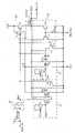
请参考图7,图7为本发明第一实施例中第n级移位寄存单元SR(n)的示意图。第一实施例的移位寄存单元SR(n)包括一输入端IN(n)、一输出端OUT(n)、一第一下拉电路11、一第二下拉电路21、一第三下拉电路31、一提升驱动电路41,以及一提升电路51。提升驱动电路41包括一晶体管开关T1,其栅极和漏极皆耦接于输入端IN(n)以接收前级移位寄存单元SR(n-m)传来的栅极驱动信号GS(n-m),而源极耦接于端点Q(n),因此能依据栅极驱动信号GS(n-m)来控制的输入端IN(n)和端点Q(n)之间的信号导通路径。提升电路51包括一晶体管开关T2,其栅极耦接于端点Q(n),漏极耦接于时脉产生器220以接收高频时脉信号CH1~CHM其中的一(例如CH1),而源极耦接于输出端OUT(n),因此能依据端点Q(n)的电位来控制时脉信号CH1和输出端OUT(n)之间的信号导通路径。Please refer to FIG. 7 . FIG. 7 is a schematic diagram of the nth stage shift register unit SR(n) in the first embodiment of the present invention. The shift register unit SR(n) of the first embodiment includes an input terminal IN(n), an output terminal OUT(n), a first pull-
第一下拉电路11包括晶体管开关T3~T6:晶体管开关T3的栅极耦接于端点K(n),漏极耦接于端点Q(n),而源极耦接于输出端OUT(n);晶体管开关T4的栅极耦接于端点K(n),漏极耦接于输出端OUT(n),而源极耦接于一提供负电位操作电压的电压源VSS;晶体管开关T5的栅极和漏极耦接于时脉产生器220以接收低频时脉信号CL1,而源极耦接于端点K(n);晶体管开关T6的栅极耦接于端点Q(n),漏极耦接于端点K(n),而源极耦接于电压源VSS。第一下拉电路11的晶体管开关T5依据低频时脉信号CL1来控制端点K(n)的电位,当端点K(n)具高电位时,端点Q(n)会通过导通的晶体管开关T3电性连接至输出端OUT(n),而输出端OUT(n)再通过导通的晶体管开关T4电性连接至电压源VSS。The first pull-
第二下拉电路21包括晶体管开关T7~T10:晶体管开关T7的栅极耦接于端点P(n),漏极耦接于端点Q(n),而源极耦接于输出端OUT(n);晶体管开关T8的栅极耦接于端点P(n),漏极耦接于输出端OUT(n),而源极耦接于电压源VSS;晶体管开关T9的栅极和漏极耦接于时脉产生器220以接收低频时脉信号CL2,而源极耦接于端点P(n);晶体管开关T10的栅极耦接于端点Q(n),漏极耦接于端点P(n),而源极耦接于电压源VSS。第二下拉电路21的晶体管开关T9依据低频时脉信号CL2来控制端点P(n)的电位,当端点P(n)具高电位时,端点Q(n)会通过导通的晶体管开关T7电性连接至输出端OUT(n),而输出端OUT(n)再通过导通的晶体管开关T8电性连接至电压源VSS。The second pull-
第三下拉电路31包括晶体管开关T11和T12:晶体管开关T11的栅极耦接于下级移位寄存单元SR(n+m)的输出端OUT(n+m)以接收回授信号FB(n),漏极耦接于端点Q(n),而源极耦接于电压源VSS;晶体管开关T12的栅极耦接于下级移位寄存单元SR(n+m)的输入端IN(n+m)以接收回授信号FB(n),漏极耦接于输出端OUT(n),而源极耦接于电压源VSS。第三下拉电路31由下级移位寄存单元SR(n+m)产生的栅极驱动信号GS(n+m)来做为回授信号FB(n),当GS(n+m)具高电位时,第n级移位寄存单元SR(n)的输出端OUT(n)和端点Q(n)皆会被拉至低电位。当m=1时,回授信号FB(n)为移位寄存单元SR(n+1)所产生的栅极驱动信号GS(n+1);当m=2时,回授信号FB(n)为移位寄存单元SR(n+2)所产生的栅极驱动信号GS(n+2),依此类推。The third pull-
请参考图8,图8为本发明第二实施例中第n级移位寄存单元SR(n)的示意图。第二实施例的移位寄存单元SR(n)包括一输入端IN(n)、一输出端OUT(n)、第一下拉电路11、第二下拉电路21、一第三下拉电路31、一提升驱动电路42,以及提升电路51。本发明第二实施例和第一实施例结构类似,不同之处在于本发明第二实施例的提升驱动电路42包括晶体管开关T1和T13。晶体管开关T1的栅极耦接于晶体管开关T13的漏极,漏极耦接于输入端IN(n)以接收栅极驱动信号GS(n-m),而源极耦接于端点Q(n);晶体管开关T13的栅极耦接于时脉产生器220以接收移位寄存单元SR(n-m)所使用的高频时脉信号CHn,而源极耦接于前级移位寄存单元SR(n-m)的端点Q(n-m)。晶体管开关T13可维持晶体管开关T1的栅极电位,以减少晶体管开关T1的漏电路径。当m=1时,晶体管开关T13的栅极耦接于时脉产生器220以接收移位寄存单元SR(n-1)所使用的高频时脉信号(例如CH4),而源极耦接于移位寄存单元SR(n-1)的端点Q(n-1);当m=2时,晶体管开关T13的栅极耦接于时脉产生器220以接收移位寄存单元SR(n-2)所使用的高频时脉信号(例如CH3),而源极耦接于移位寄存单元SR(n-2)的端点Q(n-2),依此类推。Please refer to FIG. 8 . FIG. 8 is a schematic diagram of the nth stage shift register unit SR(n) in the second embodiment of the present invention. The shift register unit SR(n) of the second embodiment includes an input terminal IN(n), an output terminal OUT(n), a first pull-
请参考图9,图9为本发明第三实施例中第n级移位寄存单元SR(n)的示意图。第三实施例的移位寄存单元SR(n)包括一输入端IN(n)、一输出端OUT(n)、一第一下拉电路13、一第二下拉电路23、一第三下拉电路31、提升驱动电路41,以及一提升电路53。本发明第三实施例和第一实施例结构类似,不同之处在于第一下拉电路13、第二下拉电路23和提升电路53的结构。本发明第三实施例的提升电路53包括晶体管开关T2和T14。晶体管开关T2的栅极耦接于端点Q(n),漏极耦接于时脉产生器220以接收高频时脉信号CH1~CHM其中之一(例如CH1),而源极耦接于输出端OUT(n),因此能依据端点Q(n)的电位来控制时脉信号CH1和输出端OUT(n)之间的信号导通路径。晶体管开关T14用来做为一载波缓冲器(carrier buffer),其栅极耦接于端点Q(n),漏极耦接于时脉产生器220以接收高频时脉信号CH1~CHM其中之一(例如CH1),而源极耦接于端点H(n),因此能依据端点Q(n)的电位来控制时脉信号CH1和端点H(n)之间的信号导通路径。本发明第一实施例将同一栅极驱动信号GS(n)传至栅极线GL(n)和下级移位寄存单元SR(n+m),本发明第三实施例则通过晶体管开关T14另产生对应于栅极驱动信号GS(n)的输入信号ST(n+m),并将栅极驱动信号GS(n)和输入信号ST(n+m)分别传至栅极线GL(n)和下级移位寄存单元SR(n+m)。换而言之,本发明第三实施例的提升驱动电路41是依据前级移位寄存单元SR(n-m)于其端点H(n-m)所产生的信号ST(n-m)来运作。同时,第一下拉电路13另包括一晶体管开关T15,而第二下拉电路23另包括一晶体管开关T16,可分别依据端点K(n)和P(n)的电位来维持端点H(n)的准位。Please refer to FIG. 9 . FIG. 9 is a schematic diagram of the nth stage shift register unit SR(n) in the third embodiment of the present invention. The shift register unit SR(n) of the third embodiment includes an input terminal IN(n), an output terminal OUT(n), a first pull-
请参考图10,图10为本发明第四实施例中第n级移位寄存单元SR(n)的示意图。第四实施例的移位寄存单元SR(n)包括一输入端IN(n)、一输出端OUT(n)、第一下拉电路13、第二下拉电路23、第三下拉电路31、提升驱动电路42,以及提升电路53。本发明第四实施例和第三实施例结构类似,不同之处在于本发明第四实施例的提升驱动电路42包括晶体管开关T1和T13。晶体管开关T1的栅极耦接于晶体管开关T13的漏极,漏极耦接于输入端IN(n)以接收信号ST(n-m),而源极耦接于端点Q(n),因此能依据前级移位寄存单元SR(n-m)于其端点H(n-m)所产生的信号ST(n-m)来运作;晶体管开关T13的栅极耦接于时脉产生器220以接收移位寄存单元SR(n-m)所使用的高频时脉信号CHn,而源极耦接于前级移位寄存单元SR(n-m)的端点Q(n-m)。晶体管开关T13可维持晶体管开关T1的栅极电位,以减少晶体管开关T1的漏电路径。当m=1时,晶体管开关T13的栅极耦接于时脉产生器220以接收移位寄存单元SR(n-1)所使用的高频时脉信号(例如CH4),而源极耦接于移位寄存单元SR(n-1)的端点Q(n-1);当m=2时,晶体管开关T13的栅极耦接于时脉产生器220以接收移位寄存单元SR(n-2)所使用的高频时脉信号(例如CH3),而源极耦接于移位寄存单元SR(n-2)的端点Q(n-2),依此类推。Please refer to FIG. 10 . FIG. 10 is a schematic diagram of an nth stage shift register unit SR(n) in a fourth embodiment of the present invention. The shift register unit SR(n) of the fourth embodiment includes an input terminal IN(n), an output terminal OUT(n), a first pull-
请参考图11,图11为本发明第一至第四实施例的液晶显示装置300运作时的时序图。图5中所示的实施例可使用低频时脉信号CL1、CL2,高频时脉信号CH1、CH2和起始脉冲信号VST来驱动移位寄存器210,而图6中所示的实施例可使用低频时脉信号CL1、CL2,高频时脉信号CH1~CH4和起始脉冲信号VST/VST1/VST2来驱动移位寄存器210,其中移位寄存单元SR(1)和SR(2)可分别由起始脉冲信号VST1和VST2来使能,或是皆由起始脉冲信号VST来使能。高频时脉信号CH1~CH4和起始脉冲信号VST1、VST2的宽度相等,但彼此之间存在着相位差。起始脉冲信号VST的宽度则是起始脉冲信号VST1/VST2宽度的两倍。每一时脉信号皆以特定频率在一高电位Vgh和一低电位Vgl之间切换,其中低频时脉信号CL1和CL2的频率远低于高频时脉信号CH1~CH4的频率(例如低频时脉信号CL1和CL2的脉波宽度可为起始脉冲信号VST1/VST2脉波宽度的100倍左右),且在同一时间低频时脉信号CL1和CL2彼此反向。OUT(n)、Q(n)、K(n)和P(n)分别代表第n级移位寄存单元SR(n)的输出端和端点Q(n)、K(n)、P(n)所提供的信号波形,在说明书后续内容中将会有详细描述。Please refer to FIG. 11 , which is a timing diagram of the operation of the liquid
本发明使用高频时脉信号CH1、两组低频时脉信号CL1、CL2和起始脉冲信号VST来驱动第一至第四实施例中的移位寄存单元SR(n)。低频时脉信号CL1和CL2彼此相位相反,当低频时脉信号CL1具高电位时,下拉动作主要由第一下拉电路11或13来负责;当低频时脉信号CL2具高电位时,下拉动作主要由第二下拉电路21或23来负责。对第n级移位寄存单元SR(n)来说,在时间点t1之前,低频时脉信号CL1维持在高电位,低频时脉信号CL2维持在低电位,此时由第一下拉电路11或13负责下拉运作。在时间点t1时,低频时脉信号CL1由高电位切换至低电位,低频时脉信号CL2由低电位切换至高电位,此时端点P(n)会通过导通的晶体管开关T9被拉至高电位,进而导通晶体管开关T7和T8以将端点Q(n)和输出端OUT(n)维持在低电位。此时下拉动作主要由第二下拉电路21或23来负责,在此段期间晶体管开关T5呈关闭,但端点K(n)仍然维持在高电位,因此第一下拉电路11或13仍会负责部份下拉运作。在时间点t2时,输入信号IN(n)(在第一至第四实施例中,IN(n)=GS(n-m))由低电位切换至高电位,此时端点Q(n)会被拉至高电位,进而导通晶体管开关T2、T6和T10,因此端点K(n)会通过导通的晶体管开关T6被拉至低电位,端点P(n)会通过导通的晶体管开关T10被拉至低电位,而栅极驱动信号GS(n)则会因为像素内晶体管开关的穿透效应被拉低至低电位Vg1。在时间点t3时,第n级移位寄存单元SR(n)开始执行上拉运作,高频时脉信号CH1由低电位切换至高电位,并通过导通的晶体管开关T2传至输出端OUT(n),以提供栅极驱动信号GS(n)至栅极线GL(n)和下级移位寄存单元SR(n+m)。在时间点t4时,第n级移位寄存单元SR(n)完成上拉运作,高频时脉信号CH1由高电位切换至低电位,输出端OUT(n)亦会随的降至低电位,晶体管开关T7和T8再度被开启,此时由第二下拉电路21继续执行下拉运作,以将端点Q(n)和输出端OUT(n)维持在低电位VSS,此时端点K(n)和端点P(n)的准位高低分别由低频时脉信号CL1和低频时脉信号CL2来决定。本发明第一至第四实施例使用不同相位的多组高频时脉信号和两组低频时脉信号来驱动移位寄存器,可增加晶体管开关的寿命和准确度。The present invention uses a high-frequency clock signal CH1, two sets of low-frequency clock signals CL1, CL2 and a start pulse signal VST to drive the shift register unit SR(n) in the first to fourth embodiments. The phases of the low-frequency clock signals CL1 and CL2 are opposite to each other. When the low-frequency clock signal CL1 has a high potential, the pull-down operation is mainly performed by the first pull-
请参考图12,图12为本发明第五实施例中第n级移位寄存单元SR(n)的示意图。第五实施例的移位寄存单元SR(n)包括一输入端IN(n)、一输出端OUT(n)、第一下拉电路11、第二下拉电路21、一快速下拉电路35、提升驱动电路41,以及提升电路51。本发明第五实施例和第一实施例结构类似,不同之处在于本发明第五实施例包括快速下拉电路35。本发明第五实施例的快速下拉电路35包括晶体管开关T11和T12:晶体管开关T11的栅极耦接于下级移位寄存单元SR(n+s)的输出端OUT(n+s)以接收回授信号FB(n),漏极耦接于端点Q(n),而源极耦接于电压源VSS;晶体管开关T12的栅极耦接于晶体管开关T11的栅极,漏极耦接于晶体管开关T2的漏极,而源极耦接于晶体管开关T2的源极。在说明书后续内容中将会详细描述本发明第五实施例的液晶显示装置300的运作情形。Please refer to FIG. 12 . FIG. 12 is a schematic diagram of the nth stage shift register unit SR(n) in the fifth embodiment of the present invention. The shift register unit SR(n) of the fifth embodiment includes an input terminal IN(n), an output terminal OUT(n), a first pull-
请参考图13,图13为本发明第六实施例中第n级移位寄存单元SR(n)的示意图。第六实施例的移位寄存单元SR(n)包括一输入端IN(n)、一输出端OUT(n)、第一下拉电路11、第二下拉电路21、快速下拉电路35、提升驱动电路42,以及提升电路51。本发明第六实施例和第二实施例结构类似,不同之处在于本发明第六实施例包括快速下拉电路35。本发明第六实施例的快速下拉电路35包括晶体管开关T11和T12:晶体管开关T11的栅极耦接于下级移位寄存单元SR(n+s)的输出端OUT(n+s)以接收回授信号FB(n),漏极耦接于端点Q(n),而源极耦接于电压源VSS;晶体管开关T12的栅极耦接于晶体管开关T11的栅极,漏极耦接于晶体管开关T2的漏极,而源极耦接于晶体管开关T2的源极。在说明书后续内容中将会详细描述本发明第六实施例的液晶显示装置300的运作情形。Please refer to FIG. 13 , which is a schematic diagram of the shift register unit SR(n) of the nth stage in the sixth embodiment of the present invention. The shift register unit SR(n) of the sixth embodiment includes an input terminal IN(n), an output terminal OUT(n), a first pull-
请参考图14,图14为本发明第七实施例中第n级移位寄存单元SR(n)的示意图。第七实施例的移位寄存单元SR(n)包括一输入端IN(n)、一输出端OUT(n)、第一下拉电路13、第二下拉电路23、快速下拉电路35、提升驱动电路41,以及提升电路53。本发明第七实施例和第三实施例结构类似,不同之处在于本发明第七实施例包括快速下拉电路35。本发明第七实施例的快速下拉电路35包括晶体管开关T11和T12:晶体管开关T11的栅极耦接于下级移位寄存单元SR(n+s)的输出端OUT(n+s)以接收回授信号FB(n),漏极耦接于端点Q(n),而源极耦接于电压源VSS;晶体管开关T12的栅极耦接于晶体管开关T11的栅极,漏极耦接于晶体管开关T2的漏极,而源极耦接于晶体管开关T2的源极。在说明书后续内容中将会详细描述本发明第七实施例的液晶显示装置300的运作情形。Please refer to FIG. 14 , which is a schematic diagram of the shift register unit SR(n) of the nth stage in the seventh embodiment of the present invention. The shift register unit SR(n) of the seventh embodiment includes an input terminal IN(n), an output terminal OUT(n), a first pull-
请参考图15,图15为本发明第八实施例中第n级移位寄存单元SR(n)的示意图。第八实施例的移位寄存单元SR(n)包括一输入端IN(n)、一输出端OUT(n)、第一下拉电路13、第二下拉电路23、快速下拉电路35、提升驱动电路41,以及提升电路53。本发明第八实施例和第四实施例结构类似,不同之处在于本发明第八实施例包括快速下拉电路35。本发明第八实施例的快速下拉电路35包括晶体管开关T11和T12:晶体管开关T11的栅极耦接于下级移位寄存单元SR(n+s)的输出端OUT(n+s)以接收回授信号FB(n),漏极耦接于端点Q(n),而源极耦接于电压源VSS;晶体管开关T12的栅极耦接于晶体管开关T11的栅极,漏极耦接于晶体管开关T2的漏极,而源极耦接于晶体管开关T2的源极。Please refer to FIG. 15 , which is a schematic diagram of the shift register unit SR(n) of the nth stage in the eighth embodiment of the present invention. The shift register unit SR(n) of the eighth embodiment includes an input terminal IN(n), an output terminal OUT(n), a first pull-
当m=1和s=1时,图16为本发明第五至第八实施例的液晶显示装置300运作时的时序图。图16中所示的实施例使用低频时脉信号CL1、CL2,高频时脉信号CH1~CH4和起始脉冲信号VST1来驱动移位寄存器210。高频时脉信号CH1~CH4和起始脉冲信号VST1的宽度相等,但彼此之间存在着相位差。每一时脉信号皆以特定频率在一高电位Vgh和一低电位Vgl之间切换,其中低频时脉信号CL1和CL2的频率远低于高频时脉信号CH1~CH4的频率,且在同一时间低频时脉信号CL1和CL2彼此反向。本发明第五至第八实施例的液晶显示装置300依据前一级栅极驱动信号GS(n-1)来产生此级栅极驱动信号GS(n),并依据下一级栅极驱动信号GS(n+1)来补偿穿透效应。在下级移位寄存单元SR(n+1)的驱动周期内,快速下拉电路35利用晶体管开关T12将栅极驱动信号GS(n)拉低至低电位Vgl,因此能补偿在前级移位寄存单元SR(n-1)的驱动周期内对像素内的数据电压所造成电容耦合效应。When m=1 and s=1, FIG. 16 is a timing diagram of the operation of the liquid
当m=1和s=2时,图17为本发明第五至第八实施例的液晶显示装置300运作时的时序图。在图17中所示的时序图中,本发明第五至第八实施例的液晶显示装置300依据前一级栅极驱动信号GS(n-1)来产生此级栅极驱动信号GS(n),并依据下两级栅极驱动信号GS(n+2)来补偿穿透效应。在下两级移位寄存单元SR(n+2)的驱动周期内,快速下拉电路35利用晶体管开关T12将栅极驱动信号GS(n)拉低至低电位Vgl,因此能补偿在前级移位寄存单元SR(n-1)的驱动周期内对像素内的数据电压所造成电容耦合效应。When m=1 and s=2, FIG. 17 is a timing diagram of the operation of the liquid
当m=2和s=2时,图18为本发明第五至第八实施例的液晶显示装置300运作时的时序图。图18中所示的时序图中,本发明第五至第八实施例的液晶显示装置300依据前两级栅极驱动信号GS(n-2)来产生此级栅极驱动信号GS(n),并依据下两级栅极驱动信号GS(n+2)来补偿穿透效应。在下两级移位寄存单元SR(n+2)的驱动周期内,快速下拉电路35利用晶体管开关T12将栅极驱动信号GS(n)拉低至低电位Vgl,因此能补偿在前两级移位寄存单元SR(n-2)的驱动周期内对像素内的数据电压所造成电容耦合效应。When m=2 and s=2, FIG. 18 is a timing diagram of the operation of the liquid
在前述实施例中,晶体管开关T1~T14可包括薄膜晶体管(thin filmtransistor,TFT)开关,或其它具类似功能的元件。前述m和n的特定值仅为了说明本发明补偿穿透效应的实施例,并不限定本发明的范畴。In the aforementioned embodiments, the transistor switches T1 - T14 may include thin film transistor (thin film transistor, TFT) switches, or other elements with similar functions. The aforementioned specific values of m and n are only for illustrating an embodiment of the present invention for compensating the penetration effect, and do not limit the scope of the present invention.
本发明使用不同相位的多组高频时脉信号和两组低频时脉信号来驱动移位寄存器,可增加晶体管开关的寿命和准确度,因此能提供液晶显示器低耗能和高可靠度的GOA驱动电路。同时,本发明亦可利用快速下拉电路的晶体管开关T12,在下级移位寄存单元SR(n+s)的驱动周期内将栅极驱动信号GS(n)拉低至低电位Vgl,因此能补偿在前级移位寄存单元SR(n-m)的驱动周期内对像素的数据电压所造成电容耦合效应。The invention uses multiple sets of high-frequency clock signals and two sets of low-frequency clock signals of different phases to drive the shift register, which can increase the service life and accuracy of transistor switches, and thus can provide a GOA with low energy consumption and high reliability for liquid crystal displays Drive circuit. At the same time, the present invention can also use the transistor switch T12 of the fast pull-down circuit to pull down the gate drive signal GS(n) to the low potential Vgl in the driving cycle of the lower shift register unit SR(n+s), so it can compensate The capacitive coupling effect is caused to the data voltage of the pixel during the driving period of the previous shift register unit SR(n-m).
以上所述仅为本发明的较佳实施例,凡依本发明申请专利范围所做的均等变化与修饰,皆应属本发明的涵盖范围。The above descriptions are only preferred embodiments of the present invention, and all equivalent changes and modifications made according to the scope of the patent application of the present invention shall fall within the scope of the present invention.
Claims (33)
Priority Applications (1)
| Application Number | Priority Date | Filing Date | Title |
|---|---|---|---|
| CN200910136921XACN101552040B (en) | 2009-04-28 | 2009-04-28 | LCD shift register |
Applications Claiming Priority (1)
| Application Number | Priority Date | Filing Date | Title |
|---|---|---|---|
| CN200910136921XACN101552040B (en) | 2009-04-28 | 2009-04-28 | LCD shift register |
Publications (2)
| Publication Number | Publication Date |
|---|---|
| CN101552040A CN101552040A (en) | 2009-10-07 |
| CN101552040Btrue CN101552040B (en) | 2011-04-13 |
Family
ID=41156228
Family Applications (1)
| Application Number | Title | Priority Date | Filing Date |
|---|---|---|---|
| CN200910136921XAActiveCN101552040B (en) | 2009-04-28 | 2009-04-28 | LCD shift register |
Country Status (1)
| Country | Link |
|---|---|
| CN (1) | CN101552040B (en) |
Families Citing this family (19)
| Publication number | Priority date | Publication date | Assignee | Title |
|---|---|---|---|---|
| CN102063874B (en)* | 2009-11-16 | 2012-12-19 | 瀚宇彩晶股份有限公司 | Gate drive circuit |
| CN101752006B (en)* | 2009-12-25 | 2012-12-12 | 友达光电股份有限公司 | Shift register |
| CN101853705B (en)* | 2010-05-27 | 2012-10-31 | 友达光电股份有限公司 | Shift Register Circuit |
| CN101976580B (en)* | 2010-10-12 | 2015-06-03 | 友达光电股份有限公司 | nth stage shift register capable of increasing driving capability and method thereof |
| CN102097074B (en)* | 2010-11-03 | 2012-08-29 | 友达光电股份有限公司 | Gate drive circuit |
| TWI437823B (en)* | 2010-12-16 | 2014-05-11 | Au Optronics Corp | Shift register circuit |
| TWI406503B (en)* | 2010-12-30 | 2013-08-21 | Au Optronics Corp | Shift register circuit |
| TWI451383B (en)* | 2011-12-05 | 2014-09-01 | Au Optronics Corp | Flat panel display, shift register and method of controlling the shift register |
| CN103187037B (en)* | 2011-12-29 | 2015-08-26 | 上海天马微电子有限公司 | Amorphous silicon grid electrode driving circuit |
| TWI505245B (en)* | 2012-10-12 | 2015-10-21 | Au Optronics Corp | Shift register |
| CN103680451B (en) | 2013-12-18 | 2015-12-30 | 深圳市华星光电技术有限公司 | For GOA circuit and the display device of liquid crystal display |
| CN104392700B (en)* | 2014-11-07 | 2016-09-14 | 深圳市华星光电技术有限公司 | Scan drive circuit for oxide semiconductor thin-film transistor |
| CN105702194B (en)* | 2016-04-26 | 2019-05-10 | 京东方科技集团股份有限公司 | A shift register unit, gate driving circuit and driving method thereof |
| WO2018020613A1 (en)* | 2016-07-27 | 2018-02-01 | 堺ディスプレイプロダクト株式会社 | Driving circuit and display device |
| CN107016972B (en)* | 2017-04-25 | 2019-08-02 | 深圳市华星光电技术有限公司 | GOA driving circuit and liquid crystal display panel |
| CN107146584B (en)* | 2017-05-05 | 2019-10-11 | 惠科股份有限公司 | Shift register circuit, waveform generation method thereof and display panel applying same |
| CN107833550A (en)* | 2017-10-27 | 2018-03-23 | 友达光电(苏州)有限公司 | Display device and its clock pulse generator |
| TWI728698B (en)* | 2020-02-14 | 2021-05-21 | 友達光電股份有限公司 | Lcd driving circuit |
| CN111583885B (en) | 2020-06-17 | 2021-11-30 | 京东方科技集团股份有限公司 | Driving method and device of shift register |
Citations (2)
| Publication number | Priority date | Publication date | Assignee | Title |
|---|---|---|---|---|
| JP2007188079A (en)* | 2006-01-10 | 2007-07-26 | Samsung Electronics Co Ltd | Gate driver, thin film transistor substrate including the same, and liquid crystal display device |
| TW200813918A (en)* | 2006-09-01 | 2008-03-16 | Au Optronics Corp | Shift register, shift register array, and display apparatus |
- 2009
- 2009-04-28CNCN200910136921XApatent/CN101552040B/enactiveActive
Patent Citations (2)
| Publication number | Priority date | Publication date | Assignee | Title |
|---|---|---|---|---|
| JP2007188079A (en)* | 2006-01-10 | 2007-07-26 | Samsung Electronics Co Ltd | Gate driver, thin film transistor substrate including the same, and liquid crystal display device |
| TW200813918A (en)* | 2006-09-01 | 2008-03-16 | Au Optronics Corp | Shift register, shift register array, and display apparatus |
Also Published As
| Publication number | Publication date |
|---|---|
| CN101552040A (en) | 2009-10-07 |
Similar Documents
| Publication | Publication Date | Title |
|---|---|---|
| CN101552040B (en) | LCD shift register | |
| TWI400686B (en) | Shift register of lcd devices | |
| TWI404036B (en) | Shift register | |
| TWI433459B (en) | Bi-directional shift register | |
| TWI410944B (en) | Shift register of a display device | |
| TWI421872B (en) | Shift register capable of reducing coupling effect | |
| CN101937718B (en) | Bidirectional shift register | |
| JP5079301B2 (en) | Shift register circuit and image display apparatus including the same | |
| CN104575436B (en) | Shift register cell, gate driver circuit and display device | |
| CN103915067B (en) | A kind of shifting deposit unit, display floater and display unit | |
| CN205595037U (en) | Shifting register, grid driving circuit and display device | |
| WO2021007932A1 (en) | Goa circuit | |
| CN101510443A (en) | Shift register capable of reducing coupling effect | |
| CN104464600A (en) | Shifting register unit, driving method of shifting register unit, shifting register circuit and display device | |
| CN106448536A (en) | Shifting register, grid driving circuit, display panel and driving method | |
| CN106228927A (en) | Shift register cell, driving method, gate driver circuit and display device | |
| CN103226980B (en) | A kind of shifting deposit unit, gate drive apparatus and display device | |
| TWI521495B (en) | Display panel, gate driver and control method | |
| CN102013244A (en) | Liquid crystal display driving circuit and related driving method | |
| CN101593561B (en) | LCD Monitor | |
| CN103280196A (en) | Shifting register and thin film transistor liquid crystal display | |
| CN101609719A (en) | Shift register for display device | |
| CN108053801A (en) | Shift register cell and its driving method, gate driving circuit and display device | |
| CN110534048B (en) | Shifting register unit, driving method, grid driving circuit and display device | |
| CN110379352A (en) | A kind of shift register and its driving method, gate driving circuit |
Legal Events
| Date | Code | Title | Description |
|---|---|---|---|
| C06 | Publication | ||
| PB01 | Publication | ||
| C10 | Entry into substantive examination | ||
| SE01 | Entry into force of request for substantive examination | ||
| C14 | Grant of patent or utility model | ||
| GR01 | Patent grant |