CN101542580B - Liquid crystal display apparatus, liquid crystal display apparatus driving method, liquid crystal display apparatus source driver, and liquid crystal display apparatus controller - Google Patents
Liquid crystal display apparatus, liquid crystal display apparatus driving method, liquid crystal display apparatus source driver, and liquid crystal display apparatus controllerDownload PDFInfo
- Publication number
- CN101542580B CN101542580BCN2007800442382ACN200780044238ACN101542580BCN 101542580 BCN101542580 BCN 101542580BCN 2007800442382 ACN2007800442382 ACN 2007800442382ACN 200780044238 ACN200780044238 ACN 200780044238ACN 101542580 BCN101542580 BCN 101542580B
- Authority
- CN
- China
- Prior art keywords
- voltage
- adjustment
- liquid crystal
- circuit
- grayscale voltage
- Prior art date
- Legal status (The legal status is an assumption and is not a legal conclusion. Google has not performed a legal analysis and makes no representation as to the accuracy of the status listed.)
- Expired - Fee Related
Links
Images


Classifications
- G—PHYSICS
- G09—EDUCATION; CRYPTOGRAPHY; DISPLAY; ADVERTISING; SEALS
- G09G—ARRANGEMENTS OR CIRCUITS FOR CONTROL OF INDICATING DEVICES USING STATIC MEANS TO PRESENT VARIABLE INFORMATION
- G09G3/00—Control arrangements or circuits, of interest only in connection with visual indicators other than cathode-ray tubes
- G09G3/20—Control arrangements or circuits, of interest only in connection with visual indicators other than cathode-ray tubes for presentation of an assembly of a number of characters, e.g. a page, by composing the assembly by combination of individual elements arranged in a matrix no fixed position being assigned to or needed to be assigned to the individual characters or partial characters
- G09G3/34—Control arrangements or circuits, of interest only in connection with visual indicators other than cathode-ray tubes for presentation of an assembly of a number of characters, e.g. a page, by composing the assembly by combination of individual elements arranged in a matrix no fixed position being assigned to or needed to be assigned to the individual characters or partial characters by control of light from an independent source
- G09G3/36—Control arrangements or circuits, of interest only in connection with visual indicators other than cathode-ray tubes for presentation of an assembly of a number of characters, e.g. a page, by composing the assembly by combination of individual elements arranged in a matrix no fixed position being assigned to or needed to be assigned to the individual characters or partial characters by control of light from an independent source using liquid crystals
- G09G3/3611—Control of matrices with row and column drivers
- G09G3/3696—Generation of voltages supplied to electrode drivers
- G—PHYSICS
- G09—EDUCATION; CRYPTOGRAPHY; DISPLAY; ADVERTISING; SEALS
- G09G—ARRANGEMENTS OR CIRCUITS FOR CONTROL OF INDICATING DEVICES USING STATIC MEANS TO PRESENT VARIABLE INFORMATION
- G09G3/00—Control arrangements or circuits, of interest only in connection with visual indicators other than cathode-ray tubes
- G09G3/20—Control arrangements or circuits, of interest only in connection with visual indicators other than cathode-ray tubes for presentation of an assembly of a number of characters, e.g. a page, by composing the assembly by combination of individual elements arranged in a matrix no fixed position being assigned to or needed to be assigned to the individual characters or partial characters
- G09G3/34—Control arrangements or circuits, of interest only in connection with visual indicators other than cathode-ray tubes for presentation of an assembly of a number of characters, e.g. a page, by composing the assembly by combination of individual elements arranged in a matrix no fixed position being assigned to or needed to be assigned to the individual characters or partial characters by control of light from an independent source
- G09G3/36—Control arrangements or circuits, of interest only in connection with visual indicators other than cathode-ray tubes for presentation of an assembly of a number of characters, e.g. a page, by composing the assembly by combination of individual elements arranged in a matrix no fixed position being assigned to or needed to be assigned to the individual characters or partial characters by control of light from an independent source using liquid crystals
- G09G3/3611—Control of matrices with row and column drivers
- G09G3/3685—Details of drivers for data electrodes
- G—PHYSICS
- G02—OPTICS
- G02F—OPTICAL DEVICES OR ARRANGEMENTS FOR THE CONTROL OF LIGHT BY MODIFICATION OF THE OPTICAL PROPERTIES OF THE MEDIA OF THE ELEMENTS INVOLVED THEREIN; NON-LINEAR OPTICS; FREQUENCY-CHANGING OF LIGHT; OPTICAL LOGIC ELEMENTS; OPTICAL ANALOGUE/DIGITAL CONVERTERS
- G02F1/00—Devices or arrangements for the control of the intensity, colour, phase, polarisation or direction of light arriving from an independent light source, e.g. switching, gating or modulating; Non-linear optics
- G02F1/01—Devices or arrangements for the control of the intensity, colour, phase, polarisation or direction of light arriving from an independent light source, e.g. switching, gating or modulating; Non-linear optics for the control of the intensity, phase, polarisation or colour
- G02F1/13—Devices or arrangements for the control of the intensity, colour, phase, polarisation or direction of light arriving from an independent light source, e.g. switching, gating or modulating; Non-linear optics for the control of the intensity, phase, polarisation or colour based on liquid crystals, e.g. single liquid crystal display cells
- G02F1/133—Constructional arrangements; Operation of liquid crystal cells; Circuit arrangements
- G02F1/1333—Constructional arrangements; Manufacturing methods
- G02F1/133397—Constructional arrangements; Manufacturing methods for suppressing after-image or image-sticking
- G—PHYSICS
- G02—OPTICS
- G02F—OPTICAL DEVICES OR ARRANGEMENTS FOR THE CONTROL OF LIGHT BY MODIFICATION OF THE OPTICAL PROPERTIES OF THE MEDIA OF THE ELEMENTS INVOLVED THEREIN; NON-LINEAR OPTICS; FREQUENCY-CHANGING OF LIGHT; OPTICAL LOGIC ELEMENTS; OPTICAL ANALOGUE/DIGITAL CONVERTERS
- G02F2203/00—Function characteristic
- G02F2203/30—Gray scale
- G—PHYSICS
- G09—EDUCATION; CRYPTOGRAPHY; DISPLAY; ADVERTISING; SEALS
- G09G—ARRANGEMENTS OR CIRCUITS FOR CONTROL OF INDICATING DEVICES USING STATIC MEANS TO PRESENT VARIABLE INFORMATION
- G09G2320/00—Control of display operating conditions
- G09G2320/02—Improving the quality of display appearance
- G09G2320/0204—Compensation of DC component across the pixels in flat panels
- G—PHYSICS
- G09—EDUCATION; CRYPTOGRAPHY; DISPLAY; ADVERTISING; SEALS
- G09G—ARRANGEMENTS OR CIRCUITS FOR CONTROL OF INDICATING DEVICES USING STATIC MEANS TO PRESENT VARIABLE INFORMATION
- G09G2320/00—Control of display operating conditions
- G09G2320/02—Improving the quality of display appearance
- G09G2320/0223—Compensation for problems related to R-C delay and attenuation in electrodes of matrix panels, e.g. in gate electrodes or on-substrate video signal electrodes
- G—PHYSICS
- G09—EDUCATION; CRYPTOGRAPHY; DISPLAY; ADVERTISING; SEALS
- G09G—ARRANGEMENTS OR CIRCUITS FOR CONTROL OF INDICATING DEVICES USING STATIC MEANS TO PRESENT VARIABLE INFORMATION
- G09G2320/00—Control of display operating conditions
- G09G2320/02—Improving the quality of display appearance
- G09G2320/0233—Improving the luminance or brightness uniformity across the screen
- G—PHYSICS
- G09—EDUCATION; CRYPTOGRAPHY; DISPLAY; ADVERTISING; SEALS
- G09G—ARRANGEMENTS OR CIRCUITS FOR CONTROL OF INDICATING DEVICES USING STATIC MEANS TO PRESENT VARIABLE INFORMATION
- G09G2320/00—Control of display operating conditions
- G09G2320/02—Improving the quality of display appearance
- G09G2320/0247—Flicker reduction other than flicker reduction circuits used for single beam cathode-ray tubes
- G—PHYSICS
- G09—EDUCATION; CRYPTOGRAPHY; DISPLAY; ADVERTISING; SEALS
- G09G—ARRANGEMENTS OR CIRCUITS FOR CONTROL OF INDICATING DEVICES USING STATIC MEANS TO PRESENT VARIABLE INFORMATION
- G09G2320/00—Control of display operating conditions
- G09G2320/02—Improving the quality of display appearance
- G09G2320/0271—Adjustment of the gradation levels within the range of the gradation scale, e.g. by redistribution or clipping
- G09G2320/0276—Adjustment of the gradation levels within the range of the gradation scale, e.g. by redistribution or clipping for the purpose of adaptation to the characteristics of a display device, i.e. gamma correction
- G—PHYSICS
- G09—EDUCATION; CRYPTOGRAPHY; DISPLAY; ADVERTISING; SEALS
- G09G—ARRANGEMENTS OR CIRCUITS FOR CONTROL OF INDICATING DEVICES USING STATIC MEANS TO PRESENT VARIABLE INFORMATION
- G09G3/00—Control arrangements or circuits, of interest only in connection with visual indicators other than cathode-ray tubes
- G09G3/20—Control arrangements or circuits, of interest only in connection with visual indicators other than cathode-ray tubes for presentation of an assembly of a number of characters, e.g. a page, by composing the assembly by combination of individual elements arranged in a matrix no fixed position being assigned to or needed to be assigned to the individual characters or partial characters
- G09G3/34—Control arrangements or circuits, of interest only in connection with visual indicators other than cathode-ray tubes for presentation of an assembly of a number of characters, e.g. a page, by composing the assembly by combination of individual elements arranged in a matrix no fixed position being assigned to or needed to be assigned to the individual characters or partial characters by control of light from an independent source
- G09G3/36—Control arrangements or circuits, of interest only in connection with visual indicators other than cathode-ray tubes for presentation of an assembly of a number of characters, e.g. a page, by composing the assembly by combination of individual elements arranged in a matrix no fixed position being assigned to or needed to be assigned to the individual characters or partial characters by control of light from an independent source using liquid crystals
- G09G3/3611—Control of matrices with row and column drivers
- G09G3/3614—Control of polarity reversal in general
Landscapes
- Engineering & Computer Science (AREA)
- Chemical & Material Sciences (AREA)
- Crystallography & Structural Chemistry (AREA)
- Physics & Mathematics (AREA)
- Computer Hardware Design (AREA)
- General Physics & Mathematics (AREA)
- Theoretical Computer Science (AREA)
- Control Of Indicators Other Than Cathode Ray Tubes (AREA)
- Liquid Crystal Display Device Control (AREA)
Abstract
Description
Translated fromChinese技术领域technical field
本发明涉及用于例如电视机装置的显示器或个人计算机的监视器等显示画面的有源矩阵型等的液晶显示装置、其采用的液晶显示装置驱动电路、液晶显示装置的源极驱动器、以及液晶显示装置的控制器。The present invention relates to a liquid crystal display device of the active matrix type or the like used for display screens such as a display of a television set or a monitor of a personal computer, a liquid crystal display device drive circuit used therein, a source driver of the liquid crystal display device, and a liquid crystal display device. The controller of the display device.
背景技术Background technique
以往,液晶显示装置具有这样的显示面板:多根扫描信号线(栅极信号线)和多根视频信号线(源极信号线)相互交叉设置,在每一个由两种信号线划分的区域中,连接于栅极信号线和源极信号线的显示用像素部多个配置成矩阵形状。各显示用像素部分别包括:设置于像素电极和对置电极之间的液晶电容Clc;以及栅极电极连接于栅极信号线,源极电极连接于源极信号线,漏极电极连接于像素电极的薄膜晶体管(TFT),根据需要设置辅助电容Cs。Conventionally, a liquid crystal display device has a display panel in which a plurality of scanning signal lines (gate signal lines) and a plurality of video signal lines (source signal lines) are intersected with each other, and each area divided by two kinds of signal lines A plurality of display pixel portions connected to the gate signal lines and the source signal lines are arranged in a matrix shape. Each pixel portion for display includes: a liquid crystal capacitor Clc disposed between the pixel electrode and the counter electrode; and the gate electrode connected to the gate signal line, the source electrode connected to the source signal line, and the drain electrode connected to the pixel The thin film transistor (TFT) of the electrode is provided with an auxiliary capacitor Cs as required.
在该液晶面板的周边部分,对每根源极信号线设置源极驱动器,源极驱动器向对应的源极信号线提供与连接于该源极信号线的各显示用像素部的视频显示相应的视频信号。为了防止液晶烧屏,该视频信号交替地以相对于对置电极电位为正极性和负极性提供。将液晶面板的这种驱动称为反转驱动。In the peripheral portion of the liquid crystal panel, a source driver is provided for each source signal line, and the source driver supplies the corresponding source signal line with video corresponding to the video display of each display pixel portion connected to the source signal line. Signal. In order to prevent liquid crystal burn-in, the video signal is alternately supplied with positive polarity and negative polarity with respect to the counter electrode potential. Such driving of the liquid crystal panel is called inversion driving.
还在该液晶面板的周边部分对每根栅极信号线设置栅极驱动器,栅极驱动器向对应的栅极信号线提供用于选择性地驱动连接于该栅极信号线的各显示用像素部的扫描信号。A gate driver is also provided for each of the gate signal lines in the peripheral portion of the liquid crystal panel, and the gate driver provides the corresponding gate signal line with a function for selectively driving each display pixel portion connected to the gate signal line. scan signal.
这每一个像素部在利用扫描信号使TFT成为导通状态时,视频信号通过TFT提供给像素电极,作为夹在两个电极之间的显示介质的液晶的取向状态根据对置电极电位和像素电极电位的电位差发生变化,作为显示画面上的多个像素部全部,在显示画面上除显示字符和图形等之外,还显示各种图像。In each pixel portion, when the TFT is turned on by the scanning signal, the video signal is supplied to the pixel electrode through the TFT, and the alignment state of the liquid crystal as a display medium sandwiched between the two electrodes depends on the potential of the opposite electrode and the pixel electrode. The potential difference of the potential changes, and various images are displayed on the display screen as well as characters, graphics, etc., as all of the plurality of pixel portions on the display screen.
在该液晶显示装置中,在各显示用像素中除液晶电容Clc和辅助电容Cs之外,还存在TFT栅极和漏极之间的寄生电容Cgd。因此,在各像素部由于栅极和漏极间的寄生电容Cgd而导致产生下述式1所示的电荷引入电压(电荷引入量)ΔV,使得实际上对液晶施加的电压变化电荷引入量ΔV。此外,在下述(式1)中,VGH为扫描信号线的栅极高电平电压,VGL为扫描信号线的栅极低电平电压。In this liquid crystal display device, in addition to the liquid crystal capacitance Clc and the auxiliary capacitance Cs, there is a parasitic capacitance Cgd between the gate and the drain of the TFT in each display pixel. Therefore, in each pixel portion, a charge introduction voltage (charge introduction amount) ΔV shown in the following
ΔV={Cgd/(Cgd+Clc+Cs)}×(VGH-VGL)...(式1)ΔV={Cgd/(Cgd+Clc+Cs)}×(VGH-VGL)...(Formula 1)
另外,由于液晶面板的显示画面内上述电荷引入量ΔV的不同,会产生可看到显示画面闪烁的现象。作为该液晶显示装置的闪烁现象的典型原因,可列举以下(1)和(2)两种原因。In addition, due to the difference in the charge introduction amount ΔV in the display screen of the liquid crystal panel, flickering of the display screen may be seen. Typical causes of the flicker phenomenon of this liquid crystal display device include the following two causes (1) and (2).
(1)在液晶面板中,由于栅极信号线上存在布线电阻和寄生电容,所以随着远离栅极信号线的信号输入端一侧,栅极信号的波形发生钝化,在各像素部由栅极和漏极间的寄生电容Cgd导致的电荷引入量ΔV产生差异。由于该电荷引入量ΔV的差异,在液晶面板的显示画面内进行正极性驱动时对液晶层施加的电压与进行负极性驱动时对液晶层施加的电压的中间值产生偏差,平衡被打破,从而发生闪烁现象。(1) In the liquid crystal panel, since there are wiring resistance and parasitic capacitance on the gate signal line, the waveform of the gate signal is blunted as the side of the signal input terminal is farther away from the gate signal line, and each pixel is formed by There is a difference in charge introduction amount ΔV due to the parasitic capacitance Cgd between the gate and the drain. Due to the difference in charge introduction amount ΔV, the intermediate value of the voltage applied to the liquid crystal layer when the positive polarity drive is performed in the display screen of the liquid crystal panel and the voltage applied to the liquid crystal layer when the negative polarity drive is performed deviates, and the balance is broken, thereby Flickering occurs.
(2)在玻璃基板(玻璃基盘)上形成像素图案的工序中,由于玻璃基板的面积的关系,难以在玻璃基板的整个面上一次形成像素图案,所以有时将其分割成多块,分多次形成像素图案。在这种情况下,因对齐(alignment)位置或图案形成装置的特性等的不同,在液晶面板的显示画面内栅极和漏极间的寄生电容Cgd产生偏差。由于该寄生电容Cgd的偏差,上述式子所示的电荷引入量ΔV产生差异,在液晶面板的显示画面内进行正极性驱动时对液晶层施加的电压与进行负极性驱动时对液晶层施加的电压的中间值产生偏差,从而发生闪烁现象。(2) In the process of forming a pixel pattern on a glass substrate (glass substrate), it is difficult to form a pixel pattern on the entire surface of the glass substrate at one time due to the area of the glass substrate. A pixel pattern is formed multiple times. In this case, variations occur in the parasitic capacitance Cgd between the gate and the drain within the display screen of the liquid crystal panel due to differences in alignment positions, characteristics of the patterning device, and the like. Due to the deviation of the parasitic capacitance Cgd, the charge introduction amount ΔV shown in the above formula differs, and the voltage applied to the liquid crystal layer when the positive polarity drive is performed in the display screen of the liquid crystal panel is different from the voltage applied to the liquid crystal layer when the negative polarity drive is performed. The intermediate value of the voltage deviates, and flicker occurs.
这里,闪烁现象(1)由栅极信号的波形钝化引起。通常,栅极信号线在显示画面内沿水平方向配置,所以通过对电荷引入量ΔV的水平方向的斜度校正正负极性的灰度电压的中间值,可以缓和闪烁现象。Here, the flicker phenomenon (1) is caused by the blunting of the waveform of the gate signal. Usually, the gate signal lines are arranged horizontally in the display screen, so the flicker phenomenon can be alleviated by correcting the intermediate value of the positive and negative gray scale voltages for the horizontal gradient of the charge introduction amount ΔV.
而闪烁现象(2)由像素图案形成工序的特性引起。因此,在进行多次像素图案形成的情况下,通过对各形成块中的电荷引入量ΔV的偏差进行校正,可以缓和闪烁现象。On the other hand, the flicker phenomenon (2) is caused by the characteristics of the pixel pattern forming process. Therefore, in the case of performing pixel pattern formation a plurality of times, the flicker phenomenon can be alleviated by correcting the variation in the charge introduction amount ΔV in each formed block.
而且,例如专利文献1中揭示了一种液晶显示装置,该液晶显示装置通过在灰度电压生成电路中组装利用电位器等的外部输入获得希望的电阻值的元件,从而能在设计了驱动电路后调整灰度特性,而不改变电路常数。Furthermore, for example,
专利文献1:日本公开专利公报“特开2001-22325号公报(公开日:平成13年1月26日)”Patent Document 1: Japanese Laid-Open Patent Publication "JP-A-2001-22325 (publication date: January 26, 2001)"
发明内容Contents of the invention
上述两种以往的闪烁现象虽然根本产生原因不同,但两者都是由液晶面板的显示画面内的电荷引入量ΔV的偏差引起的。因此,通过根据液晶面板的显示画面内的电荷引入量ΔV的偏差来调整对液晶层施加的灰度电压值,能够减轻闪烁现象。The above-mentioned two types of conventional flicker phenomena have different fundamental causes, but both are caused by variations in the charge introduction amount ΔV in the display screen of the liquid crystal panel. Therefore, the flicker phenomenon can be reduced by adjusting the gradation voltage value applied to the liquid crystal layer according to the variation of the charge introduction amount ΔV in the display screen of the liquid crystal panel.
然而,调整该灰度值引起的变化除了各灰度的正极性电压和负极性电压的中间值偏差所引起的闪烁现象程度的变化外,还会产生所谓Γ值变化那样的灰度特性变化。However, the change caused by adjusting the gradation value causes a change in the gradation characteristic called a change in the Γ value, in addition to a change in the degree of the flickering phenomenon caused by the deviation of the median value of the positive polarity voltage and the negative polarity voltage of each gradation.
而且,在以往的液晶显示装置驱动电路中,只能调整使得面板面内某一点的闪烁现象不再可见,而例如在面板中央进行调整的情况下,在面板左右正极性灰度电压和负极性灰度电压的平衡被大大地破坏,即中间值(中间电位)发生偏差,产生闪烁现象。Moreover, in the conventional liquid crystal display device drive circuit, it can only be adjusted so that the flicker phenomenon at a certain point in the panel surface is no longer visible. The balance of the gradation voltages is greatly disrupted, that is, the intermediate value (intermediate potential) deviates, and a flicker phenomenon occurs.
另外,专利文献1以在设计了驱动电路后易于调整灰度特性为目的。而且,专利文献1在调整灰度电压的情况下,通过改变各灰度的正极性电压和负极性电压的电压差来改变各灰度的电荷引入量。由于该电荷引入量的变化,存在导致闪烁现象恶化的问题。而且,专利文献1中未揭示任何输入灰度电压调整用的串行数据的方法、定时等。In addition,
本发明是鉴于上述问题而完成的,其目的在于提供一种可以使正极性灰度电压和负极性灰度电压的中间值接近使闪烁现象进一步减轻的值而不改变灰度特性的液晶显示装置驱动电路及液晶显示装置。The present invention has been made in view of the above problems, and an object of the present invention is to provide a liquid crystal display device capable of making the intermediate value of the positive polarity grayscale voltage and the negative polarity grayscale voltage close to a value at which the flickering phenomenon can be further reduced without changing the grayscale characteristics. A driving circuit and a liquid crystal display device.
为了解决上述问题,本发明的液晶显示装置驱动电路包括多个被设置在显示部周边的、与预定数量的视频信号线分别对应的驱动部,并将正极性灰度电压或负极性灰度电压作为视频信号有选择地提供给视频信号线,其中,在所述显示部中多根扫描信号线和多根视频信号线相互交叉且多个像素部呈矩阵状配置,其特征在于,各驱动部分别包括:生成显示用灰度电压的灰度电压生成电路;以及设置于该灰度电压生成电路内的第一灰度电压调整部和第二灰度电压调整部,该第一灰度电压调整部和第二灰度电压调整部一面维持正极性灰度电压和负极性灰度电压的电压差一面使这些灰度电压增加,相互独立地进行调整正极性灰度电压和负极性灰度电压的中间电位的电压调整。In order to solve the above-mentioned problems, the driving circuit of the liquid crystal display device of the present invention includes a plurality of driving parts arranged around the display part and respectively corresponding to a predetermined number of video signal lines, and the gray-scale voltage of positive polarity or the gray-scale voltage of negative polarity Selectively supplied as video signals to video signal lines, wherein in the display section, a plurality of scanning signal lines and a plurality of video signal lines intersect each other and a plurality of pixel sections are arranged in a matrix, and it is characterized in that each driving section Respectively include: a gray-scale voltage generation circuit for generating gray-scale voltages for display; and a first gray-scale voltage adjustment part and a second gray-scale voltage adjustment part arranged in the gray-scale voltage generation circuit, the first gray-scale voltage adjustment The first grayscale voltage adjustment unit and the second grayscale voltage adjustment unit increase these grayscale voltages while maintaining the voltage difference between the positive polarity grayscale voltage and the negative polarity grayscale voltage, and adjust the positive polarity grayscale voltage and the negative polarity grayscale voltage independently of each other. Voltage adjustment of intermediate potential.
为了解决上述问题,本发明的液晶显示装置驱动电路包括多个被设置在显示部周边的、与预定数量的视频信号线分别对应的驱动部,并将正极性灰度电压或负极性灰度电压作为视频信号有选择地提供给视频信号线,其中,在所述显示部中多根扫描信号线和多根视频信号线相互交叉且多个像素部呈矩阵状配置,其特征在于,各驱动部分别包括:生成显示用灰度电压的灰度电压生成电路;以及设置于该灰度电压生成电路内的第一灰度电压调整部和第二灰度电压调整部,该第一灰度电压调整部和第二灰度电压调整部一面维持正极性灰度电压和负极性灰度电压的电压差一面使这些灰度电压增加,相互独立地进行调整正极性灰度电压和负极性灰度电压的中间电位的电压调整,每一个驱动部分别使得上述正极性灰度电压和负极性灰度电压的中间电位具有斜度。In order to solve the above-mentioned problems, the driving circuit of the liquid crystal display device of the present invention includes a plurality of driving parts arranged around the display part and respectively corresponding to a predetermined number of video signal lines, and the gray-scale voltage of positive polarity or the gray-scale voltage of negative polarity Selectively supplied as video signals to video signal lines, wherein in the display section, a plurality of scanning signal lines and a plurality of video signal lines intersect each other and a plurality of pixel sections are arranged in a matrix, and it is characterized in that each driving section Respectively include: a gray-scale voltage generation circuit for generating gray-scale voltages for display; and a first gray-scale voltage adjustment part and a second gray-scale voltage adjustment part arranged in the gray-scale voltage generation circuit, the first gray-scale voltage adjustment The first grayscale voltage adjustment unit and the second grayscale voltage adjustment unit increase these grayscale voltages while maintaining the voltage difference between the positive polarity grayscale voltage and the negative polarity grayscale voltage, and adjust the positive polarity grayscale voltage and the negative polarity grayscale voltage independently of each other. For the voltage adjustment of the intermediate potential, each drive unit makes the intermediate potential of the positive polarity grayscale voltage and the negative polarity grayscale voltage have a gradient.
这里,使正极性灰度电压和负极性灰度电压增加是由于对液晶施加的电压下降相应于液晶面板的显示画面内的电荷引入量ΔV的量而对此进行补偿。Here, increasing the positive polarity grayscale voltage and the negative polarity grayscale voltage is because the voltage applied to the liquid crystal drops by an amount corresponding to the charge introduction amount ΔV in the display screen of the liquid crystal panel to compensate for this.
如果采用上述结构,则每一个驱动部都具有配备灰度电压调整部的灰度电压生成电路,所以能够以驱动部为单位进行调整正极性灰度电压和负极性灰度电压的中间电位的电压调整。而且,由于维持了正极性灰度电压和负极性灰度电压之差,所以可以防止它们的平行被破坏即灰度特性发生变化。According to the above configuration, since each driving section has a grayscale voltage generating circuit equipped with a grayscale voltage adjusting section, it is possible to adjust the intermediate potential voltage between the positive polarity grayscale voltage and the negative polarity grayscale voltage in units of driving sections. Adjustment. Furthermore, since the difference between the positive polarity grayscale voltage and the negative polarity grayscale voltage is maintained, it is possible to prevent their parallelism from being broken, that is, the grayscale characteristics from changing.
特别是灰度电压生成电路具有第一灰度电压调整部和第二灰度电压调整部,从而可以生成互不相同的调整电压。因此,通过利用这些互不相同的调整电压,能够以驱动部为单位独立地生成正极性灰度电压和负极性灰度电压的中间电位不相同的调整电压。借助于此,可以使各个驱动部的输出电压具有斜度。从而,可以生成更接近具有可减轻闪烁现象的最理想输出电压的斜度的波形的输出电压。In particular, the gradation voltage generation circuit has a first gradation voltage adjustment unit and a second gradation voltage adjustment unit, and can generate mutually different adjustment voltages. Therefore, by using these mutually different adjustment voltages, it is possible to independently generate adjustment voltages in which the intermediate potentials of the positive polarity grayscale voltage and the negative polarity grayscale voltage are different for each driving unit. With this, the output voltage of each drive unit can be given a gradient. Accordingly, it is possible to generate an output voltage closer to a waveform having a slope of the optimum output voltage that can reduce flicker.
另外,本发明的液晶显示装置驱动电路中,各个驱动部也可以在上述灰度电压生成电路的后级具有DA转换电路,该DA转换电路包括:输入从上述第一灰度电压调整部输出的正极性灰度电压和负极性灰度电压的第一输入端;以及输入从上述第二灰度电压调整部输出的正极性灰度电压和负极性灰度电压的第二输入端,在连接上述第一输入端和上述第二输入端的传输线上,在每一个和连接上述视频信号线的信号线的交叉部设置电阻。In addition, in the liquid crystal display device driving circuit of the present invention, each driving unit may include a DA conversion circuit at a subsequent stage of the gray-scale voltage generation circuit, and the DA conversion circuit includes: the first input terminal of the positive gray scale voltage and the negative polarity gray scale voltage; Resistors are provided at intersections of each of the transmission lines between the first input end and the second input end and the signal line connected to the video signal line.
如果采用上述结构,则对于DA转换电路,从不同的输入端(第一输入部和第二输入部)输入从第一灰度电压调整部输出的正极性灰度电压和负极性灰度电压以及从第二灰度电压调整部输出的正极性灰度电压和负极性灰度电压,并且在连接第一输入端和第二输入端的传输线上,在每一个与上述视频信号线的交叉部设置电阻。因此,例如对某一个灰度电压VHX,在第一灰度电压调整部生成的VHXa和在第二灰度电压调整部生成的VHXb之间,可以容易地使液晶驱动电路的输出电压具有斜度。If the above-mentioned structure is adopted, for the DA conversion circuit, the positive polarity gray-scale voltage and the negative polarity gray-scale voltage output from the first gray-scale voltage adjustment section are input from different input terminals (the first input section and the second input section) and The positive polarity grayscale voltage and the negative polarity grayscale voltage output from the second grayscale voltage adjustment part, and on the transmission line connecting the first input terminal and the second input terminal, a resistor is provided at each intersection with the above-mentioned video signal line . Therefore, for example, for a certain gradation voltage VHX, the output voltage of the liquid crystal driving circuit can be easily given a slope between VHXa generated by the first gradation voltage regulator and VHXb generated by the second gradation voltage regulator. .
另外,在本发明的液晶显示装置驱动电路中,较好的是上述第一灰度电压调整部和第二灰度电压调整部按照上述显示部内的电荷引入量ΔV的斜度,进行正极性灰度电压和负极性灰度电压的中间电位的调整。In addition, in the liquid crystal display device driving circuit of the present invention, it is preferable that the first grayscale voltage adjustment section and the second grayscale voltage adjustment section perform positive grayscale voltage adjustment according to the gradient of the charge introduction amount ΔV in the display section. The adjustment of the intermediate potential of gray scale voltage and negative polarity gray scale voltage.
如果采用上述结构,如果采用上述结构,上述第一灰度电压调整部和第二灰度电压调整部一并按照上述显示部内的电荷引入量ΔV的斜度,进行正极性灰度电压和负极性灰度电压的中间电位的调整。因此,可以更好地减轻由液晶面板的显示画面内的电荷引入量ΔV造成的闪烁现象。If the above-mentioned structure is adopted, if the above-mentioned structure is adopted, the first gray-scale voltage adjustment unit and the second gray-scale voltage adjustment unit together adjust the positive polarity gray-scale voltage and the negative polarity gray-scale voltage according to the gradient of the charge introduction amount ΔV in the above-mentioned display portion. Adjustment of the intermediate potential of the grayscale voltage. Therefore, the flicker phenomenon caused by the charge introduction amount ΔV in the display screen of the liquid crystal panel can be better alleviated.
另外,在本发明的液晶显示装置驱动电路中,较好的是上述第一灰度电压调整部具有利用外部提供的第一灰度电压调整信号生成第一输出调整电压的第一调整电压生成电路,另一方面,上述第二灰度电压调整部具有利用外部提供的第二灰度电压调整信号生成第二输出调整电压的第二调整电压生成电路。In addition, in the liquid crystal display device driving circuit of the present invention, it is preferable that the first gradation voltage adjustment unit includes a first adjustment voltage generation circuit for generating a first output adjustment voltage using a first gradation voltage adjustment signal supplied from the outside. , On the other hand, the second gradation voltage adjustment unit includes a second adjustment voltage generation circuit for generating a second output adjustment voltage using a second gradation voltage adjustment signal supplied from the outside.
还有,在本发明的液晶显示装置驱动电路中,较好的是上述各个驱动部的上述第一灰度电压调整部和第二灰度电压调整部中的某一方具有利用外部提供的第三灰度电压调整信号生成第三输出调整电压的第三调整电压生成电路,另一方则接受相邻的驱动部生成的第四输出调整电压的供给。Also, in the liquid crystal display device drive circuit of the present invention, it is preferable that one of the first grayscale voltage adjustment section and the second grayscale voltage adjustment section of each of the above-mentioned drive sections has a third grayscale voltage adjustment section provided externally. The grayscale voltage adjustment signal generates a third adjustment voltage generation circuit that generates a third output adjustment voltage, and the other is supplied with a fourth output adjustment voltage generated by an adjacent drive unit.
如果采用上述结构,设置于各个驱动部的调整电压生成电路只要一个即可,并能够从相邻的驱动部获得第三输出调整电压。因此,可以降低成本,并且只要向第一灰度电压调整部和第二灰度电压调整部的某一方输入灰度电压调整信号即可,从而可以将事先准备的数据量(即灰度电压调整信号的数据量)减半。According to the above configuration, only one adjustment voltage generation circuit is required for each driving unit, and the third output adjustment voltage can be obtained from an adjacent driving unit. Therefore, the cost can be reduced, and it is only necessary to input the gray-scale voltage adjustment signal to one of the first gray-scale voltage adjustment part and the second gray-scale voltage adjustment part, so that the amount of data prepared in advance (that is, the gray-scale voltage adjustment Signal data size) is halved.
另外,在本发明的液晶显示装置驱动电路中,较好的是上述第一调整电压生成电路和第二调整电压生成电路对每一个预先指定的任意灰度分别设置,对每一个指定的任意灰度进行中间电位的调整。In addition, in the driving circuit of the liquid crystal display device of the present invention, it is preferable that the above-mentioned first adjustment voltage generation circuit and the second adjustment voltage generation circuit are respectively provided for each pre-designated arbitrary gray level, and for each designated arbitrary gray level adjust the intermediate potential.
另外,在本发明的液晶显示装置驱动电路中,较好的是上述第三调整电压生成电路对每一个预先指定的任意灰度分别设置,对每一个指定的任意灰度进行中间电位的调整。In addition, in the liquid crystal display device driving circuit of the present invention, it is preferable that the third adjustment voltage generation circuit is separately provided for each predetermined arbitrary gray scale, and adjusts the intermediate potential for each designated arbitrary gray scale.
另外,在本发明的液晶显示装置驱动电路中,较好的是上述第一调整电压生成电路包括:电阻值可根据上述第一灰度电压调整信号的电压值而改变的可变电阻元件;以及对该可变电阻元件的输出进行缓冲的缓冲器单元。In addition, in the liquid crystal display device driving circuit of the present invention, it is preferable that the above-mentioned first adjustment voltage generating circuit includes: a variable resistance element whose resistance value can be changed according to the voltage value of the above-mentioned first gray scale voltage adjustment signal; and A buffer unit that buffers the output of this variable resistance element.
另外,在本发明的液晶显示装置驱动电路中,较好的是上述第二调整电压生成电路包括:电阻值可根据上述第二灰度电压调整信号的电压值而改变的可变电阻元件;以及对该可变电阻元件的输出进行缓冲的缓冲器单元。In addition, in the liquid crystal display device driving circuit of the present invention, it is preferable that the second adjustment voltage generation circuit includes: a variable resistance element whose resistance value can be changed according to the voltage value of the second grayscale voltage adjustment signal; and A buffer unit that buffers the output of this variable resistance element.
另外,在本发明的液晶显示装置驱动电路中,较好的是上述第三调整电压生成电路包括:电阻值可根据上述第三灰度电压调整信号的电压值而改变的可变电阻元件;以及对该可变电阻元件的输出进行缓冲的缓冲器单元。In addition, in the liquid crystal display device driving circuit of the present invention, it is preferable that the third adjustment voltage generation circuit includes: a variable resistance element whose resistance value can be changed according to the voltage value of the third grayscale voltage adjustment signal; and A buffer unit that buffers the output of this variable resistance element.
另外,在本发明的液晶显示装置驱动电路中,较好的是上述可变电阻元件为电位器。In addition, in the liquid crystal display device driving circuit of the present invention, it is preferable that the variable resistance element is a potentiometer.
另外,在本发明的液晶显示装置驱动电路中,较好的是上述灰度电压生成电路包括:根据正负基准电压生成多个正负参考电压的第一分压电路;根据正极性的参考电压生成正极性的灰度电压的第二分压电路和第三分压电路;以及根据负极性的参考电压生成负极性的灰度电压的第四分压电路和第五分压电路,上述第一灰度电压调整部将来自上述第一分压电路的参考电压增加了输出调整电压的量的电压或与之相应的电压输出到上述第二分压电路和上述第三分压电路中的某一方以及上述第四分压电路和上述第五分压电路中的某一方,上述第二灰度电压调整部将来自上述第一分压电路的参考电压增加了输出调整电压的量的电压或与之相应的电压输出到上述第二分压电路和上述第三分压电路中的另一方以及上述第四分压电路和上述第五分压电路中的另一方。In addition, in the driving circuit of the liquid crystal display device of the present invention, it is preferable that the above-mentioned gray scale voltage generating circuit includes: a first voltage dividing circuit for generating a plurality of positive and negative reference voltages according to positive and negative reference voltages; a second voltage dividing circuit and a third voltage dividing circuit for generating grayscale voltages of positive polarity; and a fourth voltage dividing circuit and a fifth voltage dividing circuit for generating grayscale voltages of negative polarity according to a reference voltage of negative polarity. The gradation voltage adjustment unit outputs a voltage obtained by increasing the reference voltage from the first voltage dividing circuit by an output adjustment voltage or a voltage corresponding thereto to one of the second voltage dividing circuit and the third voltage dividing circuit. and one of the fourth voltage dividing circuit and the fifth voltage dividing circuit, wherein the second gradation voltage adjustment unit increases the reference voltage from the first voltage dividing circuit by the output adjustment voltage or the same. The corresponding voltages are output to the other of the second voltage dividing circuit and the third voltage dividing circuit and the other of the fourth voltage dividing circuit and the fifth voltage dividing circuit.
另外,较好的是本发明的液晶显示装置包括:上述任一液晶显示装置驱动电路;控制该液晶显示装置驱动电路的控制单元;以及液晶面板。In addition, it is preferable that the liquid crystal display device of the present invention includes: any one of the liquid crystal display device driving circuits described above; a control unit for controlling the liquid crystal display device driving circuit; and a liquid crystal panel.
另外,在本发明的液晶显示装置驱动电路中,较好的是上述驱动部为源极驱动器。In addition, in the liquid crystal display device driving circuit of the present invention, it is preferable that the driving unit is a source driver.
另外,较好的是本发明的液晶显示装置的源极驱动器作为上述驱动部设置于上述任一所述的液晶显示装置驱动电路。In addition, it is preferable that the source driver of the liquid crystal display device of the present invention is provided as the driving unit in any one of the liquid crystal display device driving circuits described above.
另外,较好的是本发明的液晶显示装置的控制器包括控制液晶显示装置驱动电路的控制单元。In addition, it is preferable that the controller of the liquid crystal display device of the present invention includes a control unit for controlling the driving circuit of the liquid crystal display device.
本发明的其他目的、特征以及优点根据以下所示的叙述应该可以充分了解。另外,本发明的优点从参照附图的以下说明中应该可以明白。Other objects, features, and advantages of the present invention should be fully understood from the description below. In addition, advantages of the present invention should be apparent from the following description with reference to the accompanying drawings.
附图说明Description of drawings
图1表示本发明的实施方式,是表示液晶显示装置的结构例的框图。FIG. 1 shows an embodiment of the present invention, and is a block diagram showing a configuration example of a liquid crystal display device.
图2是表示图1的液晶显示装置中的源极驱动器的结构例的框图。FIG. 2 is a block diagram showing a configuration example of a source driver in the liquid crystal display device of FIG. 1 .
图3是表示图2所示DA转换电路的概念图。FIG. 3 is a conceptual diagram showing the DA conversion circuit shown in FIG. 2 .
图4是表示图3所示DA转换电路的一部分的图,(a)是表示图3所示DA转换电路的一部分的概念图,(b)是详细表示与(a)所示的电路等效的电路图。Fig. 4 is a diagram showing a part of the DA conversion circuit shown in Fig. 3, (a) is a conceptual diagram showing a part of the DA conversion circuit shown in Fig. 3, and (b) is a detailed diagram showing a circuit equivalent to that shown in (a) circuit diagram.
图5是表示以往的一般DA转换电路的概念图。FIG. 5 is a conceptual diagram showing a conventional general DA conversion circuit.
图6是表示图2的源极驱动器中的灰度电压生成电路的结构例的电路图。FIG. 6 is a circuit diagram showing a configuration example of a gradation voltage generation circuit in the source driver of FIG. 2 .
图7是表示图6的调整电压生成电路的结构例的电路图。FIG. 7 is a circuit diagram showing a configuration example of the adjustment voltage generation circuit shown in FIG. 6 .
图8是将图6所示的第一灰度电压生成电路36a的一部分取出表示的电路图。FIG. 8 is a circuit diagram showing a part of the first gradation
图9是表示将以往技术与比较例进行对比的事例的图。FIG. 9 is a diagram showing an example in which conventional technology is compared with a comparative example.
图10是表示将以往技术与本发明的实施方式进行对比的事例的图。FIG. 10 is a diagram showing an example in which the prior art is compared with the embodiment of the present invention.
图11是表示闪烁现象最小的中间值在一块面板内不连续的情况的图。FIG. 11 is a diagram showing a case where the minimum intermediate value of the flicker phenomenon is discontinuous within one panel.
图12是表示本发明另一实施方式中的灰度电压生成电路的结构例的电路图。FIG. 12 is a circuit diagram showing a configuration example of a gradation voltage generation circuit in another embodiment of the present invention.
图13是表示本发明又一实施方式的源极驱动器的内部结构的电路图。13 is a circuit diagram showing an internal structure of a source driver according to yet another embodiment of the present invention.
图14是表示使用图13所示的源极驱动器时形成的中间值的图。FIG. 14 is a graph showing intermediate values formed when the source driver shown in FIG. 13 is used.
标号说明Label description
3 源极驱动器(驱动部)3 Source driver (driver part)
4 控制IC(控制单元)4 Control IC (control unit)
36 灰度电压生成电路36 gray scale voltage generation circuit
36a 灰度电压生成电路36a grayscale voltage generation circuit
36b 灰度电压生成电路36b grayscale voltage generation circuit
37 DA转换电路37 DA conversion circuit
40a 第一灰度电压生成电路40a First gray scale voltage generation circuit
40b 第二灰度电压生成电路40b second grayscale voltage generating circuit
364m 可变电阻元件364m variable resistance element
364n 缓冲器(缓冲器单元)364n buffer (buffer unit)
361 第一分压电路361 The first voltage divider circuit
362a 第二分压电路362a second voltage divider circuit
362b 第四分压电路362b fourth voltage divider circuit
362c 第三分压电路362c third voltage divider circuit
362d 第五分压电路362d fifth voltage divider circuit
Rx1~Rxn 电阻Rx1~Rxn resistance
具体实施方式Detailed ways
[实施方式1][Embodiment 1]
(关于闪烁现象)(About flicker phenomenon)
本发明的实施方式的液晶显示装置是具有以消除闪烁现象为目的的驱动部(源极驱动器)的装置。因此,在说明本实施方式前,首先说明该闪烁现象。The liquid crystal display device according to the embodiment of the present invention is a device having a driving unit (source driver) for eliminating flicker phenomenon. Therefore, before describing the present embodiment, the flicker phenomenon will be described first.
产生该闪烁现象的原因有以下两个。This flickering phenomenon occurs for the following two reasons.
第一原因在于TFT液晶面板内的栅极驱动信号钝化,从而在TFT液晶基板的各像素因寄生电容Cgd引起的电荷引入量ΔV产生差异。The first reason is that the gate drive signal in the TFT liquid crystal panel is passivated, so that the charge introduction amount ΔV of each pixel of the TFT liquid crystal substrate is different due to the parasitic capacitance Cgd.
第二原因在于在TFT液晶基板上形成像素图案的工序中,由于TFT液晶基板的面积的关系而难以一次形成TFT液晶基板整个面的像素图案,所以有时将其分割成多块进行多次像素图案形成,在这种情况下,由于对齐位置或像素图案形成装置的特性等的关系,在TFT液晶基板上,在各像素因寄生电容Cgd引起的电荷引入量ΔV产生差异。The second reason is that in the process of forming the pixel pattern on the TFT liquid crystal substrate, due to the area of the TFT liquid crystal substrate, it is difficult to form the pixel pattern on the entire surface of the TFT liquid crystal substrate at one time, so sometimes it is divided into multiple blocks and the pixel pattern is performed multiple times. In this case, due to the relationship between the alignment position and the characteristics of the pixel patterning device, etc., on the TFT liquid crystal substrate, the charge introduction amount ΔV caused by the parasitic capacitance Cgd in each pixel varies.
在液晶显示装置中,将对置电位记为Vcom、将第X灰度的正极性灰度电压记为VHX、将第X灰度的负极性灰度电压记为VLX的情况下,例如,在显示第X灰度时对各像素的液晶层施加的电压VLCX用下式表示。In a liquid crystal display device, when the opposing potential is denoted as Vcom, the positive grayscale voltage of the Xth grayscale is denoted as VHX, and the negative polarity grayscale voltage of the Xth grayscale is denoted as VLX, for example, in The voltage VLCX applied to the liquid crystal layer of each pixel when displaying the Xth gradation is represented by the following formula.
VLCX=VHX-Vcom(正极性驱动时)(1)VLCX=VHX-Vcom (when driving with positive polarity) (1)
VLCX=Vcom-VLX(负极性驱动时)(2)VLCX=Vcom-VLX (when driving with negative polarity) (2)
然而,由于如上文所述在TFT液晶基板上存在由寄生电容Cgd引起的电荷引入量ΔV,所以若将电荷引入量记为ΔV,则实际上对液晶层施加的电压VLCX变成下式表示的值。However, since the charge introduction amount ΔV caused by the parasitic capacitance Cgd exists on the TFT liquid crystal substrate as described above, if the charge introduction amount is expressed as ΔV, the voltage VLCX actually applied to the liquid crystal layer becomes expressed by the following formula value.
VLCX=(VHX-ΔV)-Vcom(正极性驱动时)(3)VLCX=(VHX-ΔV)-Vcom (during positive polarity driving) (3)
VLCX=Vcom-(VLX-ΔV)(负极性驱动时)(4)VLCX=Vcom-(VLX-ΔV) (when driving with negative polarity) (4)
即VHX及VLX减小ΔV,从而使得正极性驱动时对液晶层施加的电压(也称为正极性电压)和负极性驱动时对液晶层施加的电压(也称为负极性电压)的平衡被打破,正极性驱动时对液晶层施加的电压和负极性驱动时对液晶层施加的电压的中间值产生偏差,发生闪烁现象。That is, VHX and VLX are reduced by ΔV, so that the balance of the voltage applied to the liquid crystal layer during positive polarity driving (also called positive polarity voltage) and the voltage applied to the liquid crystal layer during negative polarity driving (also called negative polarity voltage) is controlled. If it is broken, the intermediate value of the voltage applied to the liquid crystal layer during positive polarity driving and the voltage applied to the liquid crystal layer during negative polarity driving will deviate, and a flicker phenomenon will occur.
当VLCX如上式(3)和(4)那样变化时,对液晶层施加的电场发生变化,从而液晶层的透光率发生变化。伴随这一情况的发生,在液晶显示装置上显示与所希望的灰度电平不同的灰度电平,结果使得灰度特性(γ特性曲线)发生变化。When VLCX changes as in the above formulas (3) and (4), the electric field applied to the liquid crystal layer changes, whereby the light transmittance of the liquid crystal layer changes. Accompanying this occurrence, a grayscale level different from a desired grayscale level is displayed on the liquid crystal display device, and as a result, the grayscale characteristic (γ characteristic curve) changes.
另一方面,通过根据面板面内的电荷引入量ΔV的偏差来调整对液晶层施加的灰度电压值,能够减轻闪烁现象。但是,若改变灰度电压值,则除了引起各灰度的正极性电压和负极性电压的中间值的偏差导致的闪烁现象的程度的变化外,还会伴随发生灰度特性即所谓因此,要求能不改变灰度特性(γ特性曲线)地减轻闪烁现象的结构。即为了不改变灰度特性(γ特性曲线),希望将各灰度电平的VLCX固定在所希望的值,从而谋求减轻闪烁现象。On the other hand, the flicker phenomenon can be reduced by adjusting the gradation voltage value applied to the liquid crystal layer according to the variation in the charge introduction amount ΔV in the panel surface. However, if the grayscale voltage value is changed, in addition to the change in the degree of the flickering phenomenon caused by the deviation of the intermediate value of the positive polarity voltage and the negative polarity voltage of each grayscale, the so-called grayscale characteristic will also occur. A structure that can reduce the flicker phenomenon without changing the gradation characteristic (γ characteristic curve). That is, in order not to change the gradation characteristic (γ characteristic curve), it is desirable to fix VLCX at a desired value for each gradation level, thereby reducing the flicker phenomenon.
(关于液晶显示装置的结构)(About the structure of liquid crystal display device)
图1是表示本实施方式的液晶显示装置的结构例的框图。FIG. 1 is a block diagram showing a configuration example of a liquid crystal display device according to the present embodiment.
图1中,液晶显示装置10包括:液晶面板1;多个栅极驱动器2;多个源极驱动器(权利要求书所述的“驱动部”)3;以及输出视频数据信号和它们的控制信号的控制IC(控制单元)4。In Fig. 1, a liquid
液晶面板1中,多根扫描信号线(栅极信号线)和多根视频信号线(源极信号线)相互交叉设置,在每一个由两种信号线划分的区域(每一个像素部)中,连接于栅极信号线和源极信号线的多个显示用像素部配置成矩阵形状。In the
在液晶面板1的周边每隔多根(预定根数)栅极信号线设置栅极驱动器2,栅极驱动器2向对应的各栅极信号线有选择性地提供用于选择性地驱动连接于该栅极信号线的各像素部的扫描信号(栅极信号)。In the periphery of the
在液晶面板1的周边每隔多根(预定根数)源极信号线设置源极驱动器3,源极驱动器3向对应的各源极信号线有选择性地提供与连接于该源极信号线的各显示用像素部的视频显示对应的正极性和负极性的灰度电压作为视频信号(源极信号)。以此对液晶面板1进行反转驱动。A
控制IC4对栅极驱动器2提供时钟信号CK和启动脉冲信号SP等各种同步信号,并且对源极驱动器3提供时钟信号CK、启动脉冲信号SP和锁存信号LS等各种同步信号、RGB的各视频数据信号DR、DG、DB、以及用于调整各灰度的灰度电压的相互独立的第一灰度电压调整信号DVa和第二灰度电压调整信号DVb。The
即本实施方式的液晶显示装置具有如下功能(灰度电压调整功能):利用输入到各源极驱动器3的第一灰度电压调整信号DVa和第二灰度电压调整信号DVb调整各灰度的灰度电压值。That is, the liquid crystal display device of the present embodiment has a function (gray-scale voltage adjustment function) of adjusting each gray-scale voltage by using the first gray-scale voltage adjustment signal DVa and the second gray-scale voltage adjustment signal DVb input to each
在该液晶显示装置10中,利用从控制IC4输出的各种同步信号驱动源极驱动器3和栅极驱动器2,借助于此,基于视频数据信号的视频放映于构成显示部的液晶面板1。In this liquid
需要特别注意的是对各个源极驱动器3提供相互独立的灰度电压调整信号DVa和DVb这一点,基于此的作用效果将在后文中阐述。Special attention should be paid to the fact that each
(关于源极驱动器的结构)(About the structure of the source driver)
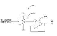
图2是表示图1的液晶显示装置10中的源极驱动器3的结构例的框图。FIG. 2 is a block diagram showing a configuration example of
图2中,源极驱动器3包括:移位寄存器电路31;输入锁存器电路32;采样存储器电路33;保持存储器电路34;电平转换器电路35;灰度电压生成电路36;DA(数字·模拟)转换电路37;以及输出电路38。In Fig. 2,
此外,本实施方式中的源极驱动器3的特征在于输入到调整电压生成电路36、DA转换电路37、以及调整电压生成电路36的第一灰度电压调整信号DVa和第二灰度电压调整信号DVb。In addition, the
向移位寄存器电路31输入来自控制IC4的时钟信号CK和启动脉冲信号SP,生成对各源极信号线的采样时钟信号并提供给采样存储器电路33。The clock signal CK and the start pulse signal SP from the
输入锁存器电路32锁存来自控制IC4的视频数据信号DR、DG和DB。The
采样存储器电路33按照来自移位寄存器电路31的采样时钟信号的时序对输入锁存器电路32锁存的视频数据信号DR、DG和DB进行采样。The
保持存储器电路34按照来自控制IC4的锁存信号LS的时序将来自采样存储器33的一个水平行量的视频数据信号(采样数据)加以锁存并保持。The holding
对电平转换器电路35提供保持存储器电路34的视频数据信号(采样数据),并将其电平转换预定的量。The video data signal (sample data) of the holding
灰度电压生成电路36由第一灰度电压生成电路36a和第二灰度电压生成电路36b构成,利用各个电路36a和36b能够生成多级显示所需的多个灰度电压,第一灰度电压生成电路36a生成第一基准灰度电压组(VH0a~VH63a、VL0a~VL63a),而第二灰度电压生成电路36b生成第二基准灰度电压组(VH0b~VH63b、VL0b~VL63b)。The gray-scale
第一基准灰度电压组(VH0a~VH63a、VL0a~VL63a)从DA转换电路37的一端输入,而第二基准灰度电压组(VH0b~VH63b、VL0b~VL63b)从DA转换电路37的另一端输入。The first reference gray-scale voltage group (VH0a-VH63a, VL0a-VL63a) is input from one end of the
第一灰度电压生成电路36a具有第一灰度电压生成部39a,该第一灰度电压生成部39a根据控制IC4提供的第一灰度电压调整信号DVa生成第一调整电压Va,根据该第一调整电压Va调整各灰度的灰度电压值。The first grayscale
另一方面,第二灰度电压生成电路36b具有第二灰度电压生成部39b,该第二灰度电压生成部39b根据控制IC4提供的第二灰度电压调整信号DVb生成第二调整电压Vb,根据该第二调整电压Vb调整各灰度的灰度电压值。On the other hand, the second gradation
这些第一调整电压Va和第二调整电压Vb成为用于将各灰度的灰度电压(第X灰度的正极性灰度电压VHX和第X灰度的负极性灰度电压VLX)调整到使其提高电荷引入量ΔV的电压。These first adjustment voltage Va and second adjustment voltage Vb are used to adjust the gray scale voltages of each gray scale (the positive polarity gray scale voltage VHX of the Xth gray scale and the negative polarity gray scale voltage VLX of the Xth gray scale) to Make it increase the voltage by the charge introduction amount ΔV.
DA转换电路37根据来自电平转换器电路35的视频数据信号,对来自灰度电压生成电路36的灰度电压进行DA转换并提供给输出电路38。The
图3是表示DA转换电路37的概念图。如该图所示,DA转换电路37包括:第一基准灰度电压组的各灰度电压的输入端和第二基准灰度电压组的各灰度电压的输入端;在这些输入端子之间的灰度基准电压传输线上对每一根源极信号线设置的64×n个电阻(Rx1~Rxn);以及对每一个电阻设置的开关电路81。FIG. 3 is a conceptual diagram showing the
从而,当源极信号线的数量为n根时,通过从DA转换电路37的两侧输入不同的基准灰度电压VHXa和VHXb,可以输出具有取决于图中的RX1~RXn的电阻比的斜度的电压。即,如果采用本实施方式的DA转换电路37,可以获得向源极驱动器3的输出端子排列的方向倾斜的电压输出。Therefore, when the number of source signal lines is n, by inputting different reference gradation voltages VHXa and VHXb from both sides of the
虽然有重复,但下面进一步详细说明本实施方式的DA转换电路37的结构。本实施方式的DA转换电路37具有以下两个特征。Although there are repetitions, the structure of the
(i)具有能够从DA转换电路37的两端或任意2点(第一输入端、第二输入端)分别输入第一基准灰度电压组(VH0a~VH63a、VL0a~VL63a)和第二基准灰度电压组(VH0b~VH63b、VL0b~VL63b)的结构。(i) It is capable of inputting the first reference gray-scale voltage group (VH0a~VH63a, VL0a~VL63a) and the second reference gray voltage group respectively from both ends of the
(ii)在DA转换电路37内部的相邻选择器电路(开关电路81)之间设置有(基准灰度电压)×(源极驱动器输出端子数)个电阻Rxn。(ii) (reference gradation voltage)×(number of source driver output terminals) resistors Rxn are provided between adjacent selector circuits (switch circuits 81 ) inside the
通过使DA转换电路37具有上述(i)和(ii)的结构,可以使例如源极驱动器输出端子在VH0a和VH0b之间具有基于电阻(旁漏电阻)R01~R0n的斜度。即,通过调整第一基准灰度电压组(VH0a~VH63a、VL0a~VL63a)和第二基准灰度电压组(VH0b~VH63b、VL0b~VL63b),能够使源极驱动器输出电压具有斜度。By making the
图3中,为了便于说明,如图4(a)所示那样,利用模拟开关(开关电路)81概念性地表示从图像数据选择模拟电压的选择器电路。此外,为了便于说明,图4(a)中省略了电阻。In FIG. 3 , for convenience of description, a selector circuit for selecting an analog voltage from image data is conceptually shown by an analog switch (switch circuit) 81 as shown in FIG. 4( a ). In addition, resistors are omitted in FIG. 4( a ) for convenience of explanation.
图4(b)是与图4(a)所示的模拟开关(开关电路)81等效的详细电路图,根据从电平转换器35输入的数字数据(图中作为一个例子为6位),在选择器电路内部设置有与数字数据的位数×基本灰度电压数相同数量的开关元件82。利用该结构,输出基于输入的图像数据的模拟电压。Fig. 4 (b) is a detailed circuit diagram equivalent to the analog switch (switching circuit) 81 shown in Fig. 4 (a), according to the digital data input from the level shifter 35 (6 bits as an example in the figure), Inside the selector circuit, the same number of switching
图5是表示作为本实施方式的DA转换电路37的参考例的一般DA转换电路37’的电路图。如该图所示,一般DA转换电路37’如图5所示,基准灰度电压组(VH0~VH63)的输入端只有一个,并且也未设置本实施方式那样的电阻。因此,由于各基本灰度电压组(VH0~VH63)在DA转换电路’内部为一定值,所以不能输出在源极驱动器输出端子方向上具有斜度的模拟电压。Fig. 5 is a circuit diagram showing a general DA conversion circuit 37' as a reference example of the
输出电路38将DA转换后的来自DA转换电路37的灰度电压作为显示电压分别输出到各源极信号线。The
(关于灰度电压生成电路的结构)(About the structure of the gradation voltage generation circuit)
图6是表示灰度电压生成电路36的简要结构的电路图。灰度电压生成电路如上文所述那样,如该图所示,具有第一灰度电压生成电路36a和第二灰度电压生成电路36b,分别具有生成第一基准灰度电压组(VH0a~VH63a、VL0a~VL63a)和第二基准灰度电压组(VH0b~VH63b、VL0b~VL63b)的作用。FIG. 6 is a circuit diagram showing a schematic configuration of the gradation
灰度电压生成电路36包括:根据正负基准电压VLS和GND生成多个正负参考电压(点A~D的各电阻分压)的第一分压电路361;暂时存储点A的电阻分压的缓冲器362a和362e;暂时存储点B的电阻分压的缓冲器362b和362f;暂时存储点C的电阻分压的缓冲器362c和362g;暂时存储点D的电阻分压的缓冲器362d和362h;利用正极性的参考电压(点A、B的各电阻分压),通过电阻分割生成正极性的第一基准灰度电压组(VH0a~VH63a)的第二分压电路363a;利用负极性的参考电压(点C、D的各电阻分压),通过电阻分割生成负极性的第一基准灰度电压组(VL63a~VL0a)的第四分压电路363b;利用正极性的参考标号(点A、B的各电阻分压),通过电阻分割生成正极性的第二基准灰度电压组(VH0b~VH63b)的第三分压电路363c;利用负极性的参考电压(点C、D的各电阻分压),通过电阻分割生成负极性的第二基准灰度电压组(VL63b~VL0b)的第五分压电路363d;将相当于寄生电容Cgd引起的电荷引入量ΔV的第一调整电压Va分别加到上述参考电压(点A~D的各电阻分压)上并输出的第一灰度电压调整部39a;以及将相当于寄生电容Cgd引起的电荷引入量ΔV的第二调整电压Vb分别加到上述参考电压(点A~D的各电阻分压)上并输出的第二灰度电压调整部39b。The grayscale voltage generating circuit 36 includes: a first voltage dividing circuit 361 that generates a plurality of positive and negative reference voltages (divided by the resistors of points A to D) according to the positive and negative reference voltages VLS and GND; Buffers 362a and 362e for temporarily storing the resistor-divided voltage of point B; buffers 362c and 362g for temporarily storing the resistor-divided voltage of point C; buffers 362d and 362g for temporarily storing the resistor-divided voltage of point D 362h; use the reference voltage of positive polarity (divided by each resistance of points A and B), and generate the second voltage dividing circuit 363a of the first reference gray-scale voltage group (VH0a~VH63a) of positive polarity through resistance division; use the negative polarity The reference voltage (divided by each resistance of points C and D) is divided by resistance to generate the fourth voltage dividing circuit 363b of the first reference gray scale voltage group (VL63a~VL0a) of negative polarity; Each resistor of A and B divides the voltage), and generates the third voltage dividing circuit 363c of the second reference gray-scale voltage group (VH0b ~ VH63b) of positive polarity through resistance division; Resistive voltage division), the fifth voltage dividing circuit 363d that generates the second reference gray scale voltage group (VL63b-VL0b) of negative polarity through resistance division; the first adjustment voltage Va corresponding to the charge introduction amount ΔV caused by the parasitic capacitance Cgd The first gradation voltage adjustment part 39a that is respectively added to the above-mentioned reference voltage (divided by each resistance of points A to D) and outputted; and the second adjustment voltage Vb corresponding to the charge introduction amount ΔV caused by the parasitic capacitance Cgd are respectively The second gradation voltage adjustment unit 39b is added to the above-mentioned reference voltage (divided by each resistance of points A to D) and outputted.
此外,在第一灰度电压调整部39a的输出侧设置第二分压电路363a和第四分压电路363b,在第二灰度电压调整部39b的输出侧设置第三分压电路363c和第五分压电路363d。In addition, the second
缓冲器362a和362e的正极性输入端连接于第一分压电路361的点A,其负极性输入端连接于输出端。缓冲器362b和362f的正极性输入端连接于第一分压电路361的点B,其负极性输入端连接于输出端。从这些缓冲器362a、362e、362b和362f输出正参考电压。The positive input terminals of the
另外,缓冲器362c和362g的正极性输入端连接于第一分压电路361的点C,其负极性输入端连接于输出端。缓冲器362d和362h的正极性输入端连接于第一分压电路361的点D,其负极性输入端连接于输出端。从这些缓冲器362c、362g、362d和362h输出负参考电压。In addition, the positive input ends of the
而且,在缓冲器362a~缓冲器362d的后级,隔着电阻设置第一灰度电压调整部39a。又在缓冲器362e~缓冲器362h的后级,隔着电阻设置第二灰度电压调整部39b。Furthermore, the first gradation
(关于灰度电压调整部的结构)(About the structure of the gradation voltage adjustment unit)
第一灰度电压调整部39a包括:根据控制IC4提供的第一灰度电压调整信号DVa生成第一灰度电压Va的第一调整电压生成电路40a;以及差动放大电路365a~365d,将用于调整电压使其提高寄生电容Cgd引起的电荷引入量ΔV的第一调整电压Va分别加到来自缓冲器362a~362d的各输出端的参考电压,分别输入到差动放大电路365a~365d的各负极性输入端。The first gradation
另一方面,第二灰度电压调整部39b包括:根据控制IC4提供的第二灰度电压调整信号DVb生成第二灰度电压Vb的第二调整电压生成电路40b;以及差动放大电路365e~365h,将用于调整电压使其提高寄生电容Cgd引起的电荷引入量ΔV的第二调整电压Vb分别加到来自缓冲器362e~362h的各输出端的参考电压,分别输入到差动放大电路365e~365h的各负极性输入端。On the other hand, the second grayscale
(关于调整电压生成电路的结构)(About the structure of the adjustment voltage generating circuit)
图7是表示第一调整电压生成电路40a的简要结构的电路图。此外,由于其只在输入信号和输出信号上不同于第二调整电压生成电路40b,内部电路结构都相同,因此省略第二调整电压生成电路40b的电路结构的说明。FIG. 7 is a circuit diagram showing a schematic configuration of the first adjustment
第一调整电压生成电路40a如该图所示,包括:电阻值可根据第一灰度电压调整信号DVa而改变的可变电阻元件364m;以及正极性输入端连接于可变电阻元件364m的输出,其负极性输入端连接于其输出端,输出第一灰度电压Va的作为缓冲器单元的缓冲器364n。As shown in the figure, the first adjustment
即,第一调整电压生成电路40a是根据第一灰度电压调整信号DVa有选择地输出Vh~0V的电压值的电路。作为该可变电阻元件364m,较好的是使用可通过输入串行数据能够获得所希望电阻值的电位器等。下面,说明使用电位器作为可变电阻元件364m的情况。That is, the first adjustment
(关于差动放大器的结构)(About the structure of the differential amplifier)
下面回到图6的说明,对第一灰度电压调整部39a的内部结构作进一步详细的说明。Returning to the description of FIG. 6 , the internal structure of the first grayscale
差动放大器365a的正极性输入端上连接隔着电阻的缓冲器362a的输出端与一端接地的电阻的另一端的接点,负极性输入端上隔着电阻连接第一调整电压生成电路40a的输出端。The positive input terminal of the
差动放大器365b的正极性输入端连接隔着电阻的缓冲器362b的输出端与一端接地的电阻的另一端的连接点,负极性输入端隔着电阻连接第一调整电压生成电路40a的输出端。The positive input terminal of the
差动放大器365c的正极性输入端连接隔着电阻的缓冲器362c的输出端与一端接地的电阻的另一端的连接点,负极性输入端隔着电阻连接第一调整电压生成电路40a的输出端。The positive input end of the
差动放大器365d的正极性输入端连接隔着电阻的缓冲器362d的输出端与一端接地的电阻的另一端的连接点,负极性输入端隔着电阻连接第一调整电压生成电路40a的输出端。The positive input terminal of the
差动放大器365e的正极性输入端连接隔着电阻的缓冲器362e的输出端与一端接地的电阻的另一端的连接点,负极性输入端隔着电阻连接第二调整电压生成电路40b的输出端。The positive input terminal of the
差动放大器365f的正极性输入端连接隔着电阻的缓冲器362f的输出端与一端接地的电阻的另一端的连接点,负极性输入端隔着电阻连接第二调整电压生成电路40b的输出端。The positive input terminal of the
差动放大器365g的正极性输入端连接隔着电阻的缓冲器362g的输出端与一端接地的电阻的另一端的连接点,负极性输入端隔着电阻连接第二调整电压生成电路40b的输出端。The positive input terminal of the
差动放大器365h的正极性输入端连接隔着电阻的缓冲器362h的输出端与一端接地的电阻的另一端的连接点,负极性输入端隔着电阻连接第二调整电压生成电路40b的输出端。The positive input terminal of the
另外,差动放大电路365a的输出端连接于第二分压电路363a中输出相对于对置电压Vcom为正极性的最大灰度电压VH0a的点I,差动放大器365b的输出端连接于第二分压电路363a中输出正极性的最小灰度电压VH63a的点J。In addition, the output terminal of the
差动放大电路365c的输出端连接于第四分压电路363b中输出相对于对置电压Vcom为负极性的最大灰度电压VL63的点K,差动放大器365d的输出端连接于第四分压电路363b中输出负极性的最小灰度电压VL0的点L。The output end of the
差动放大电路365e的输出端连接于第三分压电路363c中输出相对于对置电压Vcom为正极性的最大灰度电压VH0b的点M,差动放大器365f的输出端连接于第三分压电路363c中输出正极性的最小灰度电压VH63b的点N。The output end of the
差动放大电路365g的输出端连接于第五分压电路363d中输出相对于对置电压Vcom为负极性的最大灰度电压VL63的点O,差动放大器365h的输出端连接于第五分压电路363d中输出负极性的最小灰度电压VL0的点P。The output terminal of the
借助于此,在相对于对置电压Vcom为正极性的灰度电压中,对电压值为最大的灰度电压VH0a和电压值为最小的灰度电压VH63a的电压进行调整,在相对于Vcom为负极性的灰度电压中,对电压值为最大的灰度电压VL63a和电压值为最小的灰度电压VL0a的电压进行调整。As a result, among the grayscale voltages of positive polarity with respect to the opposing voltage Vcom, the grayscale voltage VH0a having the largest voltage value and the grayscale voltage VH63a having the smallest voltage value are adjusted. Among the grayscale voltages of negative polarity, the grayscale voltage VL63a having the largest voltage value and the grayscale voltage VL0a having the smallest voltage value are adjusted.
而且,在相对于对置电压Vcom为正极性的灰度电压中,对电压值为最大的灰度电压VH0b和电压值为最小的灰度电压VH63b的电压进行调整,在相对于Vcom为负极性的灰度电压中,对电压值为最大灰度电压VL63b和电压值为最小的灰度电压VL0b的电压进行调整。Then, among the grayscale voltages with positive polarity with respect to the opposing voltage Vcom, the grayscale voltage VH0b with the largest voltage value and the grayscale voltage VH63b with the smallest voltage value are adjusted, and the grayscale voltage with negative polarity with respect to Vcom is adjusted. Among the gray-scale voltages, the voltage whose voltage value is the maximum gray-scale voltage VL63b and the voltage value which is the smallest gray-scale voltage VL0b is adjusted.
这样,第一灰度电压调整部39a通过使其间包含任意第X灰度的正极性灰度电压VHXa的灰度电压范围的最小值(灰度电压VH63a)和最大值(灰度电压VH0a)与灰度电压范围(VH63a~VH0a)一并移位,移位量为校正电荷引入量ΔV的画面面内偏差的电压值(第一调整电压Va),还使其间包含任意第X灰度的负极性灰度电压VLXa的灰度电压范围的最小值(灰度电压VL0a)和最大值(灰度电压VL63a)与灰度电压范围(VL0a~VL63a)一并移位,移位量为校正电荷引入量ΔV的画面面内偏差的电压值(第一调整电压Va),从而保持各灰度的正极性灰度电压和负极性灰度电压的电压差,并且使正极性灰度电压和负极性灰度电压的中间电位发生移位,移位量为对电荷引入量ΔV在画面面内的偏差进行校正的电压值(调整电压Va)。此外,由于第2灰度电压调整部39b的内部结构也与第一灰度电压调整部的内部结构相同,因此省略其说明。In this way, the first gray-scale
另外,第一调整电压生成电路36a生成的第一基准灰度电压组(VH0a~VH63a、VL0a~VL63a)从DA转换电路37的左侧输入,第二调整电压生成电路36b生成的第二基准灰度电压组(VH0b~VH63b、VL0b~V63b)从右侧输入。In addition, the first reference grayscale voltage group (VH0a to VH63a, VL0a to VL63a) generated by the first adjustment
(调整电压生成电路的动作)(Operation of adjustment voltage generating circuit)
接着说明本实施方式的第一灰度电压生成电路36a的动作。Next, the operation of the first gradation
在第一调整电压生成电路40a中,利用第一灰度电压调整信号DVa控制可变电阻元件364m的电阻值,通过缓冲器364n输出第一调整电压Va。由此,第一调整电压生成电路40a根据第一灰度电压调整信号DVa有选择地输出Vh~0V电压值作为第一调整电压Va。In the first adjustment
随之,从第一灰度电压生成电路36a输出各灰度的灰度电压在差动放大电路365a~365d提高了第一调整电压Va的VH0a、VH63a、VL0a和VL63。Accordingly, the gradation voltages output from the first gradation
从而,由于VH0a、VH63a、VL0a和VL63a都发生移位,分别平均地提高了来自第一灰度电压生成电路36a的第一调整电压Va,因此既可以保持各灰度的正极性灰度电压和负极性灰度电压的电压差,又能仅改变正极性灰度电压和负极性灰度电压的中间电位(以下为中间值)。例如,可以使VH20-VL20a保持与电压调整前相同,仅改变VH20a和VL20a的中间值而不使灰度特性发生变动。Therefore, since VH0a, VH63a, VL0a, and VL63a are all shifted, the first adjustment voltage Va from the first grayscale
另外,第二灰度电压生成电路36b也是一样,VH0b、VH63b、VL0b和VL63b都发生移位,分别平均地提高了调整电压Vb,因此可以保持各灰度的正极性灰度电压和负极性灰度电压的电压差,仅改变正极性灰度电压和负极性灰度电压的中间电位(以下为中间值)。In addition, the same is true for the second grayscale
利用图8补充说明灰度电压的调整电压值。图8是将图6所示的第一灰度电压生成电路36a的一部分取出表示的电路图。The adjustment voltage value of the gradation voltage will be supplemented with reference to FIG. 8 . FIG. 8 is a circuit diagram showing a part of the first gradation
此外,为了说明方便,将输入到缓冲器362的参考电压记为VHx,将从差动放大电路365输出的电压记为VHxa,将电阻记为R1、R2、Ra、Rb。In addition, for convenience of description, the reference voltage input to the
该图中,输出电压VHxa为下式所示。In this figure, the output voltage VHxa is expressed by the following formula.
VHxa={Rb(R1+R2)}/{R2(Ra+Rb)}×VHx-(R1/R2)×Va (5)VHxa={Rb(R1+R2)}/{R2(Ra+Rb)}×VHx-(R1/R2)×Va (5)
这里,若设定R1=Ra,R2=Rb,则为下式所述。Here, if R1=Ra and R2=Rb are set, it will be expressed in the following formula.
Vhxa=VHx-(R1/R2)×Va (6)Vhxa=VHx-(R1/R2)×Va (6)
式(6)表示将从某一个基准灰度电压VHx减去由电阻R2、R1及调整电压Va决定的电压值所得的电压值作为VHxa输出。图8中仅表示对正极性的灰度基准电压的电压调整,但通过对负极性灰度基准电压VLx也进行相同的校正,能够将正负极性灰度电压的中间值调整任意电压量。通过利用本结构,根据液晶面板面内的电荷引入量ΔV对基准灰度电压的中间值进行校正,能够减轻面板面内的闪烁现象。Equation (6) indicates that the voltage value obtained by subtracting the voltage value determined by the resistors R2 and R1 and the adjustment voltage Va from a certain reference grayscale voltage VHx is output as VHxa. In FIG. 8 , only the voltage adjustment of the positive grayscale reference voltage is shown, but by performing the same correction on the negative grayscale reference voltage VLx, the intermediate value of the positive and negative grayscale voltages can be adjusted by an arbitrary voltage amount. By utilizing this configuration, the median value of the reference gradation voltage is corrected based on the charge introduction amount ΔV in the liquid crystal panel surface, thereby reducing the flicker phenomenon in the panel surface.
通过采用上述结构,可以使每一个源极驱动器独立,并设定正负极性灰度电压的中间值来谋求减轻闪烁现象。By adopting the above structure, each source driver can be made independent, and an intermediate value of the gray scale voltage of positive and negative polarities can be set to reduce the flicker phenomenon.
更详细而言,按照作为闪烁现象第一原因的栅极扫描线方向上的电荷引入量ΔV的斜度,以源极驱动器3为单位使正极性灰度电压和负极性灰度电压增加与对应源极信号线连接的像素部的电荷引入量ΔV,保持实际对液晶施加的电压(灰度电压-对置电压)原样不变,调整正负极性灰度电压的中间值,从而可以不使灰度特性(γ特性曲线)发生变动即不改变灰度特性地减轻闪烁现象的第一原因。In more detail, the positive polarity grayscale voltage and the negative polarity grayscale voltage are increased in units of the
另外,如果采用上述结构,当作为上述闪烁现象第二原因的多个区域分开转印引起的电荷引入量ΔV在面板面内的偏差为水平方向的偏差时,通过按照转印块水平方向的电荷引入量ΔV的偏差,以源极驱动器3为单位(以源极驱动器3单位的小单位独立)使正极性灰度电压和负极性灰度电压增加与对应的源极信号线连接的像素部的电荷引入量ΔV,调整正负极性灰度电压的中间值,从而可以不使灰度特性发生变动地减轻闪烁现象的第二原因。In addition, if the above-mentioned structure is adopted, when the variation in the charge introduction amount ΔV in the panel surface due to the divisional transfer of a plurality of regions, which is the second cause of the above-mentioned flicker phenomenon, is a variation in the horizontal direction, the charge in the horizontal direction of the transfer block The deviation of the introduction amount ΔV increases the positive polarity grayscale voltage and the negative polarity grayscale voltage by the pixel portion connected to the corresponding source signal line in units of the source driver 3 (independently in small units of the
而且,需要特别注意的是,在本实施方式中,对每一个源极驱动器设置第一灰度电压生成电路36a和第二灰度电压生成电路36b这两个电路,将它们的输出即第一基准灰度电压组(VH0a~VH63a、VL0a~VL63a)和第二基准灰度电压组(VH0b~VH63b、VL0b~VL63b)从图3所示那样在灰度基准传输线上配置电阻的DA转换电路37的两侧输入。Moreover, it should be noted that, in this embodiment, two circuits, the first grayscale
因此,可以使灰度电压中间值的校正值从各源极驱动器3的输出左端到输出右端以取决于电阻比的斜度连续地变化。即,以源极驱动器3为单位,可以使源极驱动器3输出的正极性灰度电压和负极性灰度电压的中间值具有斜度,通过将第一灰度电压调整信号DVa和第二灰度电压调整信号DVb调整到适当的值,可以接近最佳灰度电压中间值。因此,可以进一步减轻闪烁现象。与后文所述的比较例相比,对于减轻源极驱动器数量少的液晶显示装置或显示部大的液晶显示装置中的闪烁现象,有很大的效果。Therefore, the correction value of the intermediate value of the gradation voltage can be continuously changed with a gradient depending on the resistance ratio from the output left end to the output right end of each
如果采用本实施方式,能够对减轻寄生电容Cgd引起的电荷引入量ΔV在水平方向上的斜度所导致的闪烁现象的方法,还有对寄生电容Cgd引起的电荷引入量ΔV在水平方向上的斜度进行校正。利用图9和图10的事例对此进行详细说明。首先,将本发明人先前提出申请的发明作为[比较例]进行简单说明。If this embodiment is adopted, it is possible to reduce the flicker phenomenon caused by the slope of the charge introduction amount ΔV in the horizontal direction caused by the parasitic capacitance Cgd, and also to reduce the horizontal gradient of the charge introduction amount ΔV caused by the parasitic capacitance Cgd. Slope correction. This will be described in detail using the examples of FIGS. 9 and 10 . First, the invention that the present inventor has previously filed will be briefly described as a "comparative example".
在该[比较例]的发明中,对灰度电压生成电路分别设置灰度电压调整部和调整电压生成电路,灰度电压生成生成的基准电压也仅仅是VH0~VH63及VL0~VL63。因而,向后级DA转换电路的输入也像本实施方式那样,不是DA转换电路的两端,而仅仅是DA转换电路的一端。因此,对电荷引入量ΔV的水平方向斜度的校正也仅仅是对源极驱动器进行一对一的校正。In the invention of this [Comparative Example], the gray-scale voltage adjusting unit and the adjustment voltage generating circuit are separately provided for the gray-scale voltage generating circuit, and the reference voltages for generating the gray-scale voltage are only VH0 to VH63 and VL0 to VL63. Therefore, the input to the subsequent DA conversion circuit is not both ends of the DA conversion circuit but only one end of the DA conversion circuit as in the present embodiment. Therefore, the correction of the inclination in the horizontal direction of the charge introduction amount ΔV is only a one-to-one correction for the source driver.
假设在面板的第A行中,将闪烁现象最小的正极性灰度电压和负极性灰度电压的中间值取为位于图9中的点划线上。Assume that in row A of the panel, the median value of the positive gray voltage and the negative gray voltage with the smallest flicker phenomenon is taken to be located on the dotted line in FIG. 9 .
在无灰度电压调整功能、即无灰度电压生成电路本身的以往的的源极驱动器中,只能调整使得面板面内某一点的闪烁现象不再可见,例如图9的虚线所示,在面板中央进行调整的情况下,在面板左右,正极性灰度电压与负极性灰度电压的平衡被破坏,即中间值偏移ΔV1及ΔVr,从而产生闪烁现象。In the conventional source driver without the grayscale voltage adjustment function, that is, without the grayscale voltage generating circuit itself, it can only be adjusted so that the flicker phenomenon at a certain point in the panel surface is no longer visible, for example, as shown by the dotted line in FIG. When adjustment is performed at the center of the panel, the balance of the positive grayscale voltage and the negative grayscale voltage is disrupted on the left and right sides of the panel, that is, the median value shifts ΔV1 and ΔVr, resulting in flickering.
另一方面,若采用比较例的结构,则如实线所示,在源极驱动器内部设置灰度电压生成电路的情况下,由于可以以源极驱动器为单位,对一定的正极性负极性灰度电压的中间值进行校正,因此与以往技术相比,可以谋求改善闪烁。然而,在该比较例中,例如以源极驱动器的中央为基准进行校正闪烁现象的调整时,在各源极驱动器的端点闪烁现象最小的正极性负极性灰度电压的中间值与实际中间值存在偏差,无法进行严密的闪烁现象校正。On the other hand, if the structure of the comparative example is adopted, as shown by the solid line, in the case of providing a grayscale voltage generating circuit inside the source driver, since the source driver can be used as a unit, a certain positive polarity and negative polarity grayscale By correcting the intermediate value of the voltage, flicker can be improved compared with the conventional technology. However, in this comparative example, when the flicker correction adjustment is performed based on the center of the source driver, for example, the median value and the actual median value of the positive polarity and negative polarity gradation voltages at which the flicker phenomenon is minimized at the terminals of each source driver are There are deviations, and tight flicker correction cannot be performed.
而且,这个问题在源极驱动器数量少时或者显示画面区域大时会变得明显。Also, this problem becomes noticeable when the number of source drivers is small or when the display screen area is large.
相反地,如果采用本实施方式,以源极驱动器为单位,中间值具有预定的斜度。从而,可以在相邻的源极驱动器进行连续的中间值校正。因而,如图10中实线所示,可以更加接近点划线所示的闪烁现象最小的中间值。On the contrary, according to the present embodiment, the intermediate value has a predetermined slope in units of source drivers. Thus, continuous intermediate value correction can be performed at adjacent source drivers. Therefore, as shown by the solid line in FIG. 10 , it can be closer to the median value of the minimum flicker phenomenon shown by the dotted line.
而且,如果采用本实施方式还可以得到到如下所述效果。Furthermore, according to this embodiment mode, the effects described below can also be obtained.
如图11所示,存在闪烁现象最小的中间值在一块面板内不连续的情况。源极驱动器3(SD1)和源极驱动器3(SD2)之间、以及源极驱动器3(SD3)和源极驱动器3(SD4)之间不连续。As shown in FIG. 11 , there are cases where the median value with the smallest flicker phenomenon is not continuous within one panel. There is discontinuity between the source driver 3 ( SD1 ) and the source driver 3 ( SD2 ), and between the source driver 3 ( SD3 ) and the source driver 3 ( SD4 ).
对此,在本实施方式中,如上所述,对每一个源极驱动器3进行相互独立的两个正极性负极性灰度电压的中间值的调整。因此,例如即使在闪烁最小的中间值在一块面板内不连续的情况下,也可以如上所述,通过以源极驱动器3为单位独立地进行正极性负极性灰度电压中间值的调整,从而可以设置不连续的中间值。In contrast, in this embodiment, as described above, the intermediate value of the two independent positive and negative grayscale voltages is adjusted for each
[实施方式2][Embodiment 2]
说明本发明的另一实施方式。在本实施方式中,仅说明与上述实施方式1的不同点,省略相同部分的说明。Another embodiment of the present invention will be described. In this embodiment, only the differences from
电荷引入量ΔV在面板面内有偏差,但对TFT元件的漏极区域施加的各灰度电压值也有偏差(每一灰度电压的偏差),通常将该偏差称为ω值。The amount of charge introduction ΔV varies within the panel surface, but the value of each gradation voltage applied to the drain region of the TFT element also varies (variation per gradation voltage), and this variation is generally called ω value.
如上述实施方式1所述,通过将所有灰度电压VH0a、VH63a、VL0a和VL63a增加、调整相同电位的调整电压Va(并且将所有灰度电压VH0b、VH63b、VL0b和VL63b增加、调整相同电位的调整电压Va),从而能减轻闪烁现象,而且利用自由度高的灰度电压调整功能也能够对ω值也进行校正,能进一步减轻闪烁现象。As described in
因此,在本实施方式2中,说明能够对作为每一个灰度电压的偏差的ω值进行校正的液晶显示装置10。Therefore, in
图12是表示本发明实施方式2的液晶显示装置10中的灰度电压生成电路36的结构例的电路图。灰度电压生成电路36包括:根据正负基准电压VLS和GND生成多个正负参考电压(预定的参考电压)的第一分压电路361;暂时存储多个正负参考电压(点A~F的各电阻分压)中的某一个的缓冲器362a~3621;利用正极性的参考电压(点A~C的各电阻分压),通过电阻分压生成正极性的第一基准灰度电压组(VH0a~VH63a)的第二分压电路363a;利用负极性的参考电压(点D~F的各电阻分压),通过电阻分压生成负极性的第一基准灰度电压组(VL63a~VL0a)的第四分压电路363b;利用正极性的参考电压(点A~C的各电阻分压),通过电阻分压生成正极性的第二基准灰度电压组(VH0b~VH63b)的第三分压电路363c;利用负极性的参考电压(点D~F的各电阻分压),通过电阻分压生成负极性的第二基准灰度电压组(VL63b~VL0b)的第五分压电路363d;将相当于寄生电容Cgd引起的电荷引入量ΔV的第一调整电压Va分别加到上述参考电压(点A~F的各电阻分压)上并输出的第一灰度电压调整部39a;以及将相当于寄生电容Cgd引起的电荷引入量ΔV的第二调整电压Vb分别加到上述参考电压(点A~F的各电阻分压)上并输出的第二灰度电压调整部39b。FIG. 12 is a circuit diagram showing a configuration example of the gradation
而且,第一灰度电压调整部39a包括:根据控制IC提供的灰度电压调整信号DVa、DVXa、DV63a对每一个灰度生成独立的调整电压的第一调整电压生成电路40a-1、40a-2、40a-3;以及将来自第一调整电压生成电路40a-1、40a-2、40a-3中的某一个的调整电压和来自缓冲器362a~362f中的某一个的输出电压连接到输出端子上的差动放大电路365a~365f。Furthermore, the first gradation
另一方面,第二灰度电压调整部39b包括:根据控制IC提供的灰度电压调整信号DVb、DVXb、DV63b对每一个灰度生成独立的调整电压的第二调整电压生成电路40b-1、40b-2、40b-3;以及将来自第二调整电压生成电路40b-1、40b-2、40b-3中的某一个的调整电压和来自缓冲器362g~3621中的某一个的输出电压连接到输入端子上的差动放大电路365g~3651。On the other hand, the second gradation
为了不改变灰度特性,第一调整电压生成电路40a-1、40a-2、40a-3和第二调整电压生成电路40b-1、40b-2、40b-3使同一灰度的正极性灰度电压和负极性灰度电压在调整灰度电压时增加相同的电压值(电荷引入量ΔV),一边维持正极性灰度电压和负极性灰度电压的电压差,一边对正负极性灰度电压的中间值进行电压调整。例如,在任意第X灰度的正极性电压VH(X)和负极性电压VL(X)中,将VH(X)-VL(X)的电压值保持固定,使VH(X)和VL(X)增加输出调整电压Va的电压值,从而可以仅改变VH(X)和VL(X)的中间值。In order not to change the grayscale characteristics, the first adjustment
差动放大器365a的正极性输入端上连接隔着电阻的缓冲器362a的输出端与一端接地的电阻的另一端的连接点,负极性输入端上隔着电阻连接第一调整电压生成电路40a-1的输出端。The positive input terminal of the
差动放大器365b的正极性输入端上连接隔着电阻的缓冲器362b的输出端与一端接地的电阻的另一端的连接点,负极性输入端上隔着电阻连接第一调整电压生成电路40a-2的输出端。The positive input terminal of the
差动放大器365c的正极性输入端上连接隔着电阻的缓冲器362c的输出端与一端接地的电阻的另一端的连接点,负极性输入端上隔着电阻连接第一调整电压生成电路40a-3的输出端。The positive input terminal of the
差动放大器365d的正极性输入端上连接隔着电阻的缓冲器362d的输出端与一端接地的电阻的另一端的连接点,负极性输入端上隔着电阻连接第一调整电压生成电路40a-1的输出端。The positive input terminal of the
差动放大器365e的正极性输入端上连接隔着电阻的缓冲器362e的输出端与一端接地的电阻的另一端的连接点,负极性输入端上隔着电阻连接第一调整电压生成电路40a-2的输出端。The positive input terminal of the
差动放大器365f的正极性输入端上连接隔着电阻的缓冲器362f的输出端与一端接地的电阻的另一端的连接点,负极性输入端上隔着电阻连接第一调整电压生成电路40a-3的输出端。The positive input terminal of the
差动放大器365g的正极性输入端上连接隔着电阻的缓冲器362g的输出端与一端接地的电阻的另一端的连接点,负极性输入端上隔着电阻连接第二调整电压生成电路40b-1的输出端。The positive input terminal of the
差动放大器365h的正极性输入端上连接隔着电阻的缓冲器362h的输出端与一端接地的电阻的另一端的连接点,负极性输入端上隔着电阻连接第二调整电压生成电路40b-2的输出端。The positive input terminal of the
差动放大器365i的正极性输入端上连接隔着电阻的缓冲器362i的输出端与一端接地的电阻的另一端的连接点,负极性输入端上隔着电阻连接第二调整电压生成电路40b-3的输出端。The positive input terminal of the differential amplifier 365i is connected to the connection point between the output terminal of the
差动放大器365j的正极性输入端上连接隔着电阻的缓冲器362j的输出端与一端接地的电阻的另一端的连接点,负极性输入端上隔着电阻连接第二调整电压生成电路40b-1的输出端。The positive input terminal of the
差动放大器365k的正极性输入端上连接隔着电阻的缓冲器362k的输出端与一端接地的电阻的另一端的连接点,负极性输入端上隔着电阻连接第二调整电压生成电路40b-2的输出端。The positive input terminal of the
差动放大器3651的正极性输入端上连接隔着电阻的缓冲器3621的输出端与一端接地的电阻的另一端的连接点,负极性输入端上隔着电阻连接第二调整电压生成电路40b-3的输出端。The positive input terminal of the
差动放大电路365a的输出端连接于第二分压电路363a中输出相对于对置电压Vcom为正极性的最大灰度电压VH0a的点G。The output end of the
差动放大电路365b的输出端连接于第二分压电路363a中输出正极性的中间灰度电压VH(X)a的点H。The output terminal of the
差动放大电路365c的输出端连接于第二分压电路363a中输出正极性的最小灰度电压VH63a的点I。The output end of the
差动放大电路365d的输出端连接于第四分压电路363b中输出相对于对置电压Vcom为负极性的最大灰度电压VL63a的点J。The output end of the
差动放大电路365e的输出端连接于第四分压电路363b中输出负极性的中间灰度电压VL(X)a的点K。The output terminal of the
差动放大电路365f的输出端连接于第四分压电路363b中输出负极性的最小灰度电压VL0a的点L。The output terminal of the
差动放大电路365g的输出端连接于第三分压电路363c中输出相对于对置电压Vcom为正极性的最大灰度电压VH0b的点M。The output terminal of the
差动放大电路365h的输出端连接于第三分压电路363c中输出正极性的中间灰度电压VH(X)b的点N。The output end of the
差动放大电路365i的输出端连接于第三分压电路363c中输出正极性的最小灰度电压VH63b的点O。The output terminal of the differential amplifier circuit 365i is connected to the point O of the third
差动放大电路365j的输出端连接于第五分压电路363d中输出相对于对置电压Vcom为负极性的最大灰度电压VL63b的点P。The output end of the
差动放大电路365k的输出端连接于第五分压电路363d中输出负极性的中间灰度电压VL(X)b的点Q。The output end of the
差动放大电路3651的输出端连接于第五分压电路363d中输出负极性的最小灰度电压VL0b的点R。The output end of the
借助于此,对每一灰度,调整在相对于对置电压Vcom为正极性的灰度电压中电压值为最大的灰度电压VH0、中间的灰度电压VH(X)、和最小的灰度电压VH63的电压,调整在相对于Vcom为负极性的灰度电压中电压值为最大的灰度电压VL63、中间的灰度电压VL(X)、和最小的灰度电压VL0的电压。With this, for each gradation, the gradation voltage VH0 having the largest voltage value, the middle gradation voltage VH(X), and the smallest gradation voltage among the gradation voltages having a positive polarity with respect to the counter voltage Vcom are adjusted. To adjust the voltage of the gray scale voltage VH63, the gray scale voltage VL63 with the largest voltage value, the intermediate gray scale voltage VL(X), and the smallest gray scale voltage VL0 among the gray scale voltages with negative polarity relative to Vcom.
如上所述,如果采用本实施方式2,由于能够对每一个灰度独立地调整正负极性灰度电压的中间值,所以即使各灰度间电荷引入量ΔV存在偏差(ω值),或各灰度间闪烁现象最小的正负极性灰度电压的中间值存在偏差(ω值)的情况下,也可以通过输入对各灰度互不相同的灰度电压调整信号DV0a、DVXa和DV63a,从而进一步减轻闪烁现象。As described above, according to
因此,控制上述电压调整的控制IC4作为根据使液晶面板中成为驱动对象的像素部显示的灰度来设定上述中间值的移位量的单元起到作用。Therefore, the
此外,对第0灰度、第X灰度和第63灰度这三个灰度设置灰度电压调整功能,但未必一定要是这三个,也能够通过对三个以上的更多灰度设置灰度电压调整功能来对各灰度间产生的偏差进行更加详细的调整。In addition, the grayscale voltage adjustment function is set for the three grayscales of the 0th grayscale, the Xth grayscale, and the 63rd grayscale, but it does not necessarily have to be these three, and it is also possible to set more grayscales of three or more Grayscale voltage adjustment function to adjust the deviation between each grayscale in more detail.
[实施方式3][Embodiment 3]
下面说明本发明的又一实施方式。Still another embodiment of the present invention will be described below.
与实施方式2相同,省略说明实施方式1和2中已说明的部分和相同的部分。As in
在实施方式1中,对所有源极驱动器3,各设置两个调整电压生成电路40a和40b。相反地,在本实施方式中如图13所示,对源极驱动器3各设置一个调整电压生成电路(第三灰度电压生成电路)40c。更具体地说,仅在源极驱动器3的右端(或左端)设置调整电压生成电路40c。In
下面对仅在源极驱动器3的右端设置调整电压生成电路40c的情况进行说明。Next, a case where the adjustment voltage generation circuit 40c is provided only at the right end of the
在这种情况下,设置于第一源极驱动器3右侧的第二源极驱动器3接受来自设置于第一源极驱动器3右端的调整电压生成电路40a或40b的输出(Vd:第四输出调整电压),在调整电压生成电路40c中根据第三灰度电压生成信号VDc生成第三输出调整电压Vc。根据这些调整电压V进行电压调整,使其发生移位,移位量为根据这些调整电压V校正电荷引入量ΔV的画面面内偏差的电压值(第一调整电压Va)。In this case, the
假设对于每一个源极驱动器3,调整电压生成电路40c内部的可变电阻元件364m的电阻值有误差的情况下,由于每一个源极驱动器的校正量存在差异,因此调整电压不连续,从而可能发生显示不均匀。Assuming that there is an error in the resistance value of the
相反地,如果采用上述结构,在相邻的源极驱动器3之间调整电压V相等。因此,相邻的源极驱动器3的每一个的校正量都相等,而且可以防止调整电压不连续。即,可以形成图14所示的中间值,从而能够进行更加无不协调感的校正。On the contrary, if the above structure is adopted, the adjustment voltage V is equal between
而且,由于调整电压生成电路40c只要有一个即可,从而可以降低成本。另外,还有使得输入到源极驱动器3的灰度电压调整信号DVc的数据量也只要一半即可的效果。Furthermore, since only one adjustment voltage generating circuit 40c is required, cost can be reduced. In addition, there is an effect that the data amount of the gradation voltage adjustment signal DVc input to the
本发明不限于上述各实施方式,可在权利要求书所示的范围内进行种种变更,适当组合不同实施方式分别揭示的技术手段而得到的实施方式也包含在本发明的技术范围内。The present invention is not limited to the above-mentioned embodiments, and various changes can be made within the range shown in the claims. Embodiments obtained by appropriately combining technical means disclosed in different embodiments are also included in the technical scope of the present invention.
如上所述,本发明的液晶显示装置驱动电路包括多个被设置在显示部周边的、与预定数量的视频信号线分别对应的驱动部,并将正极性灰度电压或负极性灰度电压作为视频信号有选择地提供给视频信号线,其中,在所述显示部中多根扫描信号线和多根视频信号线相互交叉且多个像素部呈矩阵状配置,其中,各驱动部分别包括:生成显示用灰度电压的灰度电压生成电路;以及设置于该灰度电压生成电路内的第一灰度电压调整部和第二灰度电压调整部,该第一灰度电压调整部和第二灰度电压调整部一面维持正极性灰度电压和负极性灰度电压的电压差一面使这些灰度电压增加,相互独立地进行调整正极性灰度电压和负极性灰度电压的中间电位的电压调整。As described above, the driving circuit of the liquid crystal display device of the present invention includes a plurality of driving parts arranged around the display part and respectively corresponding to a predetermined number of video signal lines, and the gray-scale voltage of the positive polarity or the gray-scale voltage of the negative polarity is used as The video signal is selectively provided to the video signal lines, wherein in the display part, a plurality of scanning signal lines and a plurality of video signal lines cross each other and a plurality of pixel parts are arranged in a matrix, wherein each driving part includes: a gray-scale voltage generation circuit for generating gray-scale voltages for display; and a first gray-scale voltage adjustment unit and a second gray-scale voltage adjustment unit provided in the gray-scale voltage generation circuit, the first gray-scale voltage adjustment unit and the second gray-scale voltage adjustment unit The two-gradation voltage adjustment section increases these gray-scale voltages while maintaining the voltage difference between the positive-polarity gray-scale voltage and the negative-polarity gray-scale voltage, and adjusts the intermediate potential between the positive-polarity gray-scale voltage and the negative-polarity gray-scale voltage independently of each other. voltage adjustment.
如上所述,本发明的液晶显示装置驱动电路包括多个被设置在显示部周边的、与预定数量的视频信号线分别对应的驱动部,并将正极性灰度电压或负极性灰度电压作为视频信号有选择地提供给视频信号线,其中,在所述显示部中多根扫描信号线和多根视频信号线相互交叉且多个像素部呈矩阵状配置,其中,各驱动部分别包括:生成显示用灰度电压的灰度电压生成电路;以及设置于该灰度电压生成电路内的第一灰度电压调整部和第二灰度电压调整部,该第一灰度电压调整部和第二灰度电压调整部一面维持正极性灰度电压和负极性灰度电压的电压差一面使这些灰度电压增加,相互独立地进行调整正极性灰度电压和负极性灰度电压的中间电位的电压调整,每一个驱动部分别使得上述正极性灰度电压和负极性灰度电压的中间电位具有斜度。As described above, the driving circuit of the liquid crystal display device of the present invention includes a plurality of driving parts arranged around the display part and respectively corresponding to a predetermined number of video signal lines, and the gray-scale voltage of the positive polarity or the gray-scale voltage of the negative polarity is used as The video signal is selectively provided to the video signal lines, wherein in the display part, a plurality of scanning signal lines and a plurality of video signal lines cross each other and a plurality of pixel parts are arranged in a matrix, wherein each driving part includes: a gray-scale voltage generation circuit for generating gray-scale voltages for display; and a first gray-scale voltage adjustment unit and a second gray-scale voltage adjustment unit provided in the gray-scale voltage generation circuit, the first gray-scale voltage adjustment unit and the second gray-scale voltage adjustment unit The two-gradation voltage adjustment section increases these gray-scale voltages while maintaining the voltage difference between the positive-polarity gray-scale voltage and the negative-polarity gray-scale voltage, and adjusts the intermediate potential between the positive-polarity gray-scale voltage and the negative-polarity gray-scale voltage independently of each other. In the voltage adjustment, each drive unit makes the intermediate potential of the above-mentioned positive grayscale voltage and negative polarity grayscale voltage have a gradient.
因而,具有如下效果:能够提供一种可以使正极性灰度电压和负极性灰度电压的中间值更接近使闪烁现象进一步减轻的值而不改变灰度特性的液晶显示装置驱动电路。Therefore, there is an effect of providing a liquid crystal display device driving circuit capable of bringing the intermediate value of the positive gray scale voltage and the negative polarity gray scale voltage closer to a value at which the flicker phenomenon can be further reduced without changing the gray scale characteristics.
“发明的详细说明”这一栏的内容中叙述的具体实施方式或实施例都只是清楚地表示出本发明的技术内容,但不应狭义地理解为只限于这样的具体例子,在本发明的精神和后文记载的权利要求书的范围内可以进行各种变更而实施。The specific implementation methods or examples described in the column of "Detailed Description of the Invention" are only to clearly show the technical content of the present invention, but should not be narrowly understood as being limited to such specific examples. Various modifications can be made within the spirit and scope of the claims described below.
工业上的实用性Industrial Applicability
本发明可以用于装载电容方式的触摸面板的显示器。The present invention can be used for a display equipped with a capacitive touch panel.
Claims (20)
Applications Claiming Priority (3)
| Application Number | Priority Date | Filing Date | Title |
|---|---|---|---|
| JP2006322630 | 2006-11-29 | ||
| JP322630/2006 | 2006-11-29 | ||
| PCT/JP2007/063724WO2008065773A1 (en) | 2006-11-29 | 2007-07-10 | Liquid crystal display apparatus, liquid crystal display apparatus driving circuit, liquid crystal display apparatus source driver, and liquid crystal display apparatus controller |
Publications (2)
| Publication Number | Publication Date |
|---|---|
| CN101542580A CN101542580A (en) | 2009-09-23 |
| CN101542580Btrue CN101542580B (en) | 2012-05-09 |
Family
ID=39467572
Family Applications (1)
| Application Number | Title | Priority Date | Filing Date |
|---|---|---|---|
| CN2007800442382AExpired - Fee RelatedCN101542580B (en) | 2006-11-29 | 2007-07-10 | Liquid crystal display apparatus, liquid crystal display apparatus driving method, liquid crystal display apparatus source driver, and liquid crystal display apparatus controller |
Country Status (3)
| Country | Link |
|---|---|
| US (1) | US8284123B2 (en) |
| CN (1) | CN101542580B (en) |
| WO (1) | WO2008065773A1 (en) |
Families Citing this family (21)
| Publication number | Priority date | Publication date | Assignee | Title |
|---|---|---|---|---|
| JP5114326B2 (en)* | 2008-07-17 | 2013-01-09 | 株式会社ジャパンディスプレイイースト | Display device |
| US8743047B2 (en) | 2008-11-26 | 2014-06-03 | Sharp Kabushiki Kaisha | Liquid crystal display device, method for driving liquid crystal display device, and television receiver |
| JP5341103B2 (en) | 2008-11-26 | 2013-11-13 | シャープ株式会社 | Liquid crystal display device, driving method of liquid crystal display device, and television receiver |
| WO2010073775A1 (en) | 2008-12-25 | 2010-07-01 | シャープ株式会社 | Display device and display device drive method |
| BRPI0924202A2 (en)* | 2009-01-30 | 2016-01-19 | Sharp Kk | video device and method to control the same |
| BRPI1016181A2 (en)* | 2009-04-24 | 2016-04-19 | Sharp Kk | liquid crystal display device |
| CN102201206B (en)* | 2010-03-26 | 2012-10-31 | 北京京东方光电科技有限公司 | Method and device for regulating pixel voltage symmetry |
| JP2012189764A (en)* | 2011-03-10 | 2012-10-04 | Panasonic Liquid Crystal Display Co Ltd | Liquid crystal display device |
| JP2012189767A (en) | 2011-03-10 | 2012-10-04 | Panasonic Liquid Crystal Display Co Ltd | Liquid crystal display device |
| JP2012189765A (en) | 2011-03-10 | 2012-10-04 | Panasonic Liquid Crystal Display Co Ltd | Liquid crystal display device |
| JP6058289B2 (en)* | 2012-06-05 | 2017-01-11 | サターン ライセンシング エルエルシーSaturn Licensing LLC | Display device, imaging device, and gradation voltage generation circuit |
| KR20150102803A (en)* | 2014-02-28 | 2015-09-08 | 삼성디스플레이 주식회사 | Display apparatus |
| US9564105B2 (en)* | 2014-06-11 | 2017-02-07 | Texas Instruments Incorporated | Programmable level shifter for LCD systems |
| JP2016139079A (en)* | 2015-01-29 | 2016-08-04 | セイコーエプソン株式会社 | Display device, electro-optic device, and electronic apparatus |
| KR20170036176A (en)* | 2015-09-23 | 2017-04-03 | 삼성디스플레이 주식회사 | Display panel driving apparatus, method of driving display panel using the display panel driving apparatus and display apparatus having the display panel driving apparatus |
| CN105096901A (en)* | 2015-09-24 | 2015-11-25 | 深圳市华星光电技术有限公司 | Display device and image display method thereof |
| US10339882B2 (en)* | 2015-12-09 | 2019-07-02 | L-3 Communications Corporation | Fault-tolerant AMLCD display |
| CN110322852B (en)* | 2019-06-14 | 2020-10-16 | 深圳市华星光电技术有限公司 | Gamma voltage output circuit, step-down repairing method thereof and source driver |
| CN114550665B (en)* | 2020-11-24 | 2023-09-15 | 京东方科技集团股份有限公司 | Liquid crystal display device, driving system thereof and driving method thereof |
| US12148339B2 (en)* | 2022-03-30 | 2024-11-19 | Novatek Microelectronics Corp. | Gamma voltage generator, source driver and display apparatus |
| CN118692412B (en)* | 2024-08-28 | 2024-12-03 | 海的电子科技(苏州)有限公司 | VCOM voltage regulating method and equipment of liquid crystal panel and storage medium |
Citations (6)
| Publication number | Priority date | Publication date | Assignee | Title |
|---|---|---|---|---|
| JPH0792937A (en) | 1993-07-29 | 1995-04-07 | Hitachi Ltd | Liquid crystal driving method and liquid crystal display device |
| JPH07333576A (en) | 1994-06-09 | 1995-12-22 | Mitsubishi Electric Corp | Liquid crystal display device and driving method thereof |
| US6151005A (en)* | 1992-10-07 | 2000-11-21 | Hitachi, Ltd. | Liquid-crystal display system having a driver circuit capable of multi-color display |
| WO2003039132A1 (en)* | 2001-10-08 | 2003-05-08 | Indigo N.V. | Gradation smoothing |
| CN1453758A (en)* | 2002-04-25 | 2003-11-05 | 夏普株式会社 | Display driving apparatus and display with the same apparatus |
| CN1726528A (en)* | 2002-12-26 | 2006-01-25 | 卡西欧计算机株式会社 | Display drive device and drive control method |
Family Cites Families (15)
| Publication number | Priority date | Publication date | Assignee | Title |
|---|---|---|---|---|
| JP2912480B2 (en) | 1991-08-22 | 1999-06-28 | シャープ株式会社 | Display device drive circuit |
| JP2989952B2 (en) | 1992-01-13 | 1999-12-13 | 日本電気株式会社 | Active matrix liquid crystal display |
| KR100343513B1 (en)* | 1993-07-29 | 2003-05-27 | 히다찌디바이스엔지니어링 가부시기가이샤 | Liquid crystal driving method and apparatus |
| JPH11133919A (en) | 1997-10-27 | 1999-05-21 | Advanced Display Inc | Liquid crystal display |
| US5877717A (en)* | 1997-12-15 | 1999-03-02 | Industrial Technology Research Institute | D/A converter with a Gamma correction circuit |
| US6310592B1 (en)* | 1998-12-28 | 2001-10-30 | Samsung Electronics Co., Ltd. | Liquid crystal display having a dual bank data structure and a driving method thereof |
| TW521241B (en)* | 1999-03-16 | 2003-02-21 | Sony Corp | Liquid crystal display apparatus, its driving method, and liquid crystal display system |
| JP2001022325A (en) | 1999-07-08 | 2001-01-26 | Advanced Display Inc | Liquid crystal display device |
| JP2001100711A (en) | 1999-07-26 | 2001-04-13 | Sharp Corp | Source driver, source line drive circuit and liquid crystal display device using the same |
| JP4056672B2 (en) | 2000-02-29 | 2008-03-05 | シャープ株式会社 | Semiconductor device and display device module |
| JP2002366112A (en) | 2001-06-07 | 2002-12-20 | Hitachi Ltd | Liquid crystal driving device and liquid crystal display device |
| KR100864491B1 (en) | 2002-05-16 | 2008-10-20 | 삼성전자주식회사 | Driving device of liquid crystal display |
| JP2004094014A (en) | 2002-09-02 | 2004-03-25 | Hitachi Displays Ltd | Display device |
| JP4738867B2 (en) | 2004-10-22 | 2011-08-03 | ルネサスエレクトロニクス株式会社 | Display device drive device |
| JP2008107369A (en) | 2005-02-01 | 2008-05-08 | Sharp Corp | Liquid crystal display device and liquid crystal display driving circuit |
- 2007
- 2007-07-10CNCN2007800442382Apatent/CN101542580B/ennot_activeExpired - Fee Related
- 2007-07-10USUS12/312,834patent/US8284123B2/ennot_activeExpired - Fee Related
- 2007-07-10WOPCT/JP2007/063724patent/WO2008065773A1/enactiveApplication Filing
Patent Citations (6)
| Publication number | Priority date | Publication date | Assignee | Title |
|---|---|---|---|---|
| US6151005A (en)* | 1992-10-07 | 2000-11-21 | Hitachi, Ltd. | Liquid-crystal display system having a driver circuit capable of multi-color display |
| JPH0792937A (en) | 1993-07-29 | 1995-04-07 | Hitachi Ltd | Liquid crystal driving method and liquid crystal display device |
| JPH07333576A (en) | 1994-06-09 | 1995-12-22 | Mitsubishi Electric Corp | Liquid crystal display device and driving method thereof |
| WO2003039132A1 (en)* | 2001-10-08 | 2003-05-08 | Indigo N.V. | Gradation smoothing |
| CN1453758A (en)* | 2002-04-25 | 2003-11-05 | 夏普株式会社 | Display driving apparatus and display with the same apparatus |
| CN1726528A (en)* | 2002-12-26 | 2006-01-25 | 卡西欧计算机株式会社 | Display drive device and drive control method |
Also Published As
| Publication number | Publication date |
|---|---|
| US8284123B2 (en) | 2012-10-09 |
| CN101542580A (en) | 2009-09-23 |
| US20100045708A1 (en) | 2010-02-25 |
| WO2008065773A1 (en) | 2008-06-05 |
Similar Documents
| Publication | Publication Date | Title |
|---|---|---|
| CN101542580B (en) | Liquid crystal display apparatus, liquid crystal display apparatus driving method, liquid crystal display apparatus source driver, and liquid crystal display apparatus controller | |
| US8094108B2 (en) | Liquid crystal display device and liquid crystal display driving circuit | |
| JP4193771B2 (en) | Gradation voltage generation circuit and drive circuit | |
| KR100884993B1 (en) | LCD and its driving method | |
| KR101277937B1 (en) | LCD and drive method thereof | |
| US8514158B2 (en) | Liquid crystal driving device | |
| US8872858B2 (en) | Method of driving display panel and display apparatus for performing the same | |
| JP5049101B2 (en) | Liquid crystal display | |
| KR100475167B1 (en) | Liquid crystal display and method of driving the same | |
| CN110085178B (en) | Liquid crystal display device, controller and driving method thereof | |
| US20120120044A1 (en) | Liquid crystal display device and method for driving the same | |
| JP2001100711A (en) | Source driver, source line drive circuit and liquid crystal display device using the same | |
| US8698787B2 (en) | Method for generating a gamma voltage, driving circuit therefor, and display device | |
| KR101438586B1 (en) | LCD and method of compensating gamma curve of the same | |
| KR20110024993A (en) | Driving device of liquid crystal display and driving method thereof | |
| US20070279364A1 (en) | Liquid crystal display device, data driver thereof, and driving method thereof | |
| JP3519323B2 (en) | Driving method of liquid crystal display device | |
| JP2008122745A (en) | Method for creating gamma correction table, driving circuit for display device, and electro-optical device | |
| KR101146376B1 (en) | Liquid Crystal Display device and method for driving the same | |
| JP4567838B2 (en) | Liquid crystal display | |
| WO2009128281A1 (en) | Circuit for driving liquid crystal display apparatus | |
| JP4053198B2 (en) | Liquid crystal display | |
| KR101127850B1 (en) | Driving circuit of liquid crystal display device | |
| KR100898792B1 (en) | LCD Display | |
| KR101107676B1 (en) | Pixel Charge Compensation Circuit and Method of Liquid Crystal Display |
Legal Events
| Date | Code | Title | Description |
|---|---|---|---|
| C06 | Publication | ||
| PB01 | Publication | ||
| C10 | Entry into substantive examination | ||
| SE01 | Entry into force of request for substantive examination | ||
| C14 | Grant of patent or utility model | ||
| GR01 | Patent grant | ||
| CF01 | Termination of patent right due to non-payment of annual fee | ||
| CF01 | Termination of patent right due to non-payment of annual fee | Granted publication date:20120509 Termination date:20210710 |