CN101528364A - Layer switching for ultrasound transducer arrays - Google Patents
Layer switching for ultrasound transducer arraysDownload PDFInfo
- Publication number
- CN101528364A CN101528364ACNA2007800385661ACN200780038566ACN101528364ACN 101528364 ACN101528364 ACN 101528364ACN A2007800385661 ACNA2007800385661 ACN A2007800385661ACN 200780038566 ACN200780038566 ACN 200780038566ACN 101528364 ACN101528364 ACN 101528364A
- Authority
- CN
- China
- Prior art keywords
- passive
- layers
- transmit
- switching
- electrode
- Prior art date
- Legal status (The legal status is an assumption and is not a legal conclusion. Google has not performed a legal analysis and makes no representation as to the accuracy of the status listed.)
- Granted
Links
Images


Classifications
- B—PERFORMING OPERATIONS; TRANSPORTING
- B06—GENERATING OR TRANSMITTING MECHANICAL VIBRATIONS IN GENERAL
- B06B—METHODS OR APPARATUS FOR GENERATING OR TRANSMITTING MECHANICAL VIBRATIONS OF INFRASONIC, SONIC, OR ULTRASONIC FREQUENCY, e.g. FOR PERFORMING MECHANICAL WORK IN GENERAL
- B06B1/00—Methods or apparatus for generating mechanical vibrations of infrasonic, sonic, or ultrasonic frequency
- B06B1/02—Methods or apparatus for generating mechanical vibrations of infrasonic, sonic, or ultrasonic frequency making use of electrical energy
- B06B1/06—Methods or apparatus for generating mechanical vibrations of infrasonic, sonic, or ultrasonic frequency making use of electrical energy operating with piezoelectric effect or with electrostriction
- B06B1/0607—Methods or apparatus for generating mechanical vibrations of infrasonic, sonic, or ultrasonic frequency making use of electrical energy operating with piezoelectric effect or with electrostriction using multiple elements
- B06B1/0622—Methods or apparatus for generating mechanical vibrations of infrasonic, sonic, or ultrasonic frequency making use of electrical energy operating with piezoelectric effect or with electrostriction using multiple elements on one surface
- B06B1/064—Methods or apparatus for generating mechanical vibrations of infrasonic, sonic, or ultrasonic frequency making use of electrical energy operating with piezoelectric effect or with electrostriction using multiple elements on one surface with multiple active layers
- G—PHYSICS
- G01—MEASURING; TESTING
- G01S—RADIO DIRECTION-FINDING; RADIO NAVIGATION; DETERMINING DISTANCE OR VELOCITY BY USE OF RADIO WAVES; LOCATING OR PRESENCE-DETECTING BY USE OF THE REFLECTION OR RERADIATION OF RADIO WAVES; ANALOGOUS ARRANGEMENTS USING OTHER WAVES
- G01S15/00—Systems using the reflection or reradiation of acoustic waves, e.g. sonar systems
- G01S15/88—Sonar systems specially adapted for specific applications
- G01S15/89—Sonar systems specially adapted for specific applications for mapping or imaging
- G01S15/8906—Short-range imaging systems; Acoustic microscope systems using pulse-echo techniques
- G—PHYSICS
- G10—MUSICAL INSTRUMENTS; ACOUSTICS
- G10K—SOUND-PRODUCING DEVICES; METHODS OR DEVICES FOR PROTECTING AGAINST, OR FOR DAMPING, NOISE OR OTHER ACOUSTIC WAVES IN GENERAL; ACOUSTICS NOT OTHERWISE PROVIDED FOR
- G10K11/00—Methods or devices for transmitting, conducting or directing sound in general; Methods or devices for protecting against, or for damping, noise or other acoustic waves in general
- G10K11/18—Methods or devices for transmitting, conducting or directing sound
- G10K11/26—Sound-focusing or directing, e.g. scanning
- G10K11/34—Sound-focusing or directing, e.g. scanning using electrical steering of transducer arrays, e.g. beam steering
- G10K11/341—Circuits therefor
- G10K11/346—Circuits therefor using phase variation
- H—ELECTRICITY
- H10—SEMICONDUCTOR DEVICES; ELECTRIC SOLID-STATE DEVICES NOT OTHERWISE PROVIDED FOR
- H10N—ELECTRIC SOLID-STATE DEVICES NOT OTHERWISE PROVIDED FOR
- H10N30/00—Piezoelectric or electrostrictive devices
- H10N30/80—Constructional details
Landscapes
- Engineering & Computer Science (AREA)
- Physics & Mathematics (AREA)
- Acoustics & Sound (AREA)
- Radar, Positioning & Navigation (AREA)
- Remote Sensing (AREA)
- Multimedia (AREA)
- Computer Networks & Wireless Communication (AREA)
- General Physics & Mathematics (AREA)
- Mechanical Engineering (AREA)
- Ultra Sonic Daignosis Equipment (AREA)
- Transducers For Ultrasonic Waves (AREA)
- Investigating Or Analyzing Materials By The Use Of Ultrasonic Waves (AREA)
Abstract
Description
Translated fromChinese技术领域technical field
[0001]该本实施例涉及超声换能器(ultrasound transducer)。尤其,提供了在换能器中层的切换使用。[0001] This present embodiment relates to an ultrasonic transducer (ultrasound transducer). In particular, a switching use of layers in a transducer is provided.
背景技术Background technique
[0002]双层换能器提供了传统的换能器中不可获得的各种操作模式。通过同相地(in phase)驱动元件的两个层然后不同相地对两个层的所接收的信号求和来提供谐波模式(harmonic mode)。所发射的声场(acoustic field)具有低的二次谐波含量,并且接收的能量包括在采用基频抑制的二次谐波处的信息。[0002] Dual layer transducers offer various modes of operation not available in conventional transducers. The harmonic mode is provided by driving two layers of elements in phase and then summing the received signals of the two layers out of phase. The transmitted acoustic field has a low second harmonic content and the received energy includes information at the second harmonic suppressed with the fundamental frequency.
[0003]美国专利号5,957,851公开了使用分层的声学元件发射和接收信号的方法。然而,该方法不将声学元件的两个层用于发射和接收二者。当换能器元件的两个层被使用时,可以获得更佳的谐波模式性能。[0003] US Patent No. 5,957,851 discloses a method of transmitting and receiving signals using layered acoustic elements. However, this approach does not use two layers of acoustic elements for both transmission and reception. Better harmonic mode performance can be obtained when two layers of transducer elements are used.
[0004]以双通道计数(count)为代价来实现双层元件的增加的灵活性。每个元件均具有两层换能器材料,并且每个层与不同的系统通道连接。发射/接收通道专用于每个双层元件的每个层。对于每个层来说可以独立地优化发射机波形和接收机信号处理以便实现双层换能器的全电势。额外的通道连接可以由该主机系统处理,但是这需要具有每个元件两个通道的主机系统。一种替代是将信号处理电子装置构建到换能器里以便将发射脉冲引导到元件的一个层或两个层。该信号处理电子装置定相(phase)并且组合来自层的所接收的信号。该换能器中的有源部件可能需要额外的信号线用于控制,可能需要额外功率,并且可能产生不希望的热。[0004] The increased flexibility of dual-layer elements is achieved at the expense of dual channel counts. Each element has two layers of transducer material, and each layer is connected to a different system channel. Transmit/receive channels are dedicated to each layer of each bilayer component. The transmitter waveform and receiver signal processing can be optimized independently for each layer to achieve the full potential of the double layer transducer. Additional channel connections can be handled by the host system, but this requires a host system with two channels per element. An alternative is to build signal processing electronics into the transducer to direct the transmit pulses to one or both layers of the element. The signal processing electronics phase and combine the received signals from the layers. Active components in the transducer may require additional signal wires for control, may require additional power, and may generate undesired heat.
[0005]在该主机超声系统中,发射/接收(T/R)开关将每个通道分离成接收和发射通道。该T/R开关是无源开关,例如在美国专利号6,269,052中所公开的。例如高压CMOS模拟开关的有源开关元件,不能非常快地调整(settle)。这使得难以在扫描行期间切换它们,例如在用于对行进行扫瞄的发射与接收事件之间。操作有源开关元件还需要源自该超声系统的周密定时的控制信号。[0005] In the mainframe ultrasound system, a transmit/receive (T/R) switch separates each channel into receive and transmit channels. The T/R switch is a passive switch, such as disclosed in US Patent No. 6,269,052. Active switching elements, such as high voltage CMOS analog switches, cannot settle very quickly. This makes it difficult to switch them during scanning of the rows, for example between transmit and receive events for scanning the rows. Operating active switching elements also requires carefully timed control signals originating from the ultrasound system.
发明内容Contents of the invention
[0006]作为介绍,以下描述的优选实施例包括用于多层换能器元件的方法和系统。多层换能器利用每个元件仅一个系统通道来操作。无源切换对于发射操作与对于接收操作来说以不同的方式连接层,例如对于发射以并联的方式连接层而对于接收以串联的方式连接层。可以使用任何无源切换,例如限流和限压电路。[0006] By way of introduction, the preferred embodiments described below include methods and systems for multilayer transducer elements. Multilayer transducers operate with only one system channel per element. Passive switching connects the layers differently for transmit operation than for receive operation, eg connects the layers in parallel for transmit and in series for receive. Any passive switching such as current limiting and voltage limiting circuits can be used.
[0007]作为对层的无源切换的替换或附加方案,调谐可以被无源切换。根据电压电平在发射与接收操作之间无源切换不同的调谐。[0007] As an alternative or in addition to passive switching of layers, the tuning may be passively switched. The different tunings are passively switched between transmit and receive operation depending on the voltage level.
[0008]在第一方面,提供了一种超声换能器元件系统。至少一个超声换能器元件至少具有第一和第二层换能器材料。发射波束生成器通道与该元件连接以便第一和第二层二者响应于相同的发射波形。接收波束生成器通道与该元件连接以便由第一和第二层二者产生的信号被提供给接收波束生成器通道。[0008] In a first aspect, an ultrasonic transducer element system is provided. At least one ultrasound transducer element has at least first and second layers of transducer material. A transmit beamformer channel is connected to the element so that both the first and second layers respond to the same transmit waveform. A receive beamformer channel is connected to the element so that signals generated by both the first and second layers are provided to the receive beamformer channel.
[0009]在第二方面,提供了一种超声换能器元件系统。至少一个超声换能器元件至少具有第一和第二层换能器材料。无源限流电路连接在第一及第二层中的至少一个和系统通道之间。[0009] In a second aspect, an ultrasonic transducer element system is provided. At least one ultrasound transducer element has at least first and second layers of transducer material. A passive current limiting circuit is connected between at least one of the first and second layers and the system channel.
[0010]在第三方面,提供一种用于在超声和电能之间转换的方法。将较高电压发射波形应用到元件。利用该元件产生较低电压接收波形。根据电压电平无源切换该元件中的换能器材料的第一和第二层的并联和串联连接。[0010] In a third aspect, a method for converting between ultrasound and electrical energy is provided. Applies a higher voltage launch waveform to the component. Use this element to generate lower voltage receive waveforms. The parallel and series connections of the first and second layers of transducer material in the element are passively switched according to the voltage level.
[0011]在第四方面,提供一种用于调谐超声元件的方法。将发射波形应用于元件。响应于该应用利用该元件产生接收波形。根据该应用和产生无源切换调谐。[0011] In a fourth aspect, a method for tuning an ultrasonic element is provided. Applies a launch waveform to a component. A receive waveform is generated with the element in response to the application. Passive switching is tuned according to the application and generation.
[0012]本发明由以下权利要求限定,本部分不应当被视为对那些权利要求的限制。本发明进一步的方面和优点在以下结合优选实施例一起被论述并且可能随后被独立地或组合地要求保护。[0012] The present invention is defined by the following claims, and this section should not be taken as a limitation on those claims. Further aspects and advantages of the invention are discussed below in conjunction with preferred embodiments and may be claimed subsequently independently or in combination.
附图说明Description of drawings
[0013]所述部件和图不一定按比例,而是强调说明本发明的原理。此外,在所述图中,同样的附图标记贯穿不同的视图指定相应的部分。[0013] The components and drawings are not necessarily to scale, emphasis instead being placed upon illustrating the principles of the invention. Furthermore, in the figures, like reference numerals designate corresponding parts throughout the different views.
[0014]图1是多层元件换能器系统的第一实施例的电路图;Fig. 1 is the circuit diagram of the first embodiment of multilayer element transducer system;
[0015]图2是依据两个实施例的无源开关元件的图形电路图;[0015] FIG. 2 is a graphical circuit diagram of passive switching elements according to two embodiments;
[0016]图3是针对一个操作模式无源切换的图1的电路图;Fig. 3 is the circuit diagram of Fig. 1 for passive switching of an operation mode;
[0017]图4是针对另一操作模式无源切换的图1的电路图;Fig. 4 is the circuit diagram of Fig. 1 for passive switching of another mode of operation;
[0018]图5是多层元件换能器系统的第二实施例的电路图;[0018] FIG. 5 is a circuit diagram of a second embodiment of a multilayer element transducer system;
[0019]图6是多层元件换能器系统的第三实施例的电路图;[0019] FIG. 6 is a circuit diagram of a third embodiment of a multilayer element transducer system;
[0020]图7无源切换的调谐电路的一个实施例的电路图;The circuit diagram of an embodiment of the tuning circuit of Fig. 7 passive switching;
[0021]图8无源切换的调谐电路的另一个实施例的电路图;以及The circuit diagram of another embodiment of the tuning circuit of Fig. 8 passive switching; And
[0022]图9是多层元件换能器系统的第四实施例的电路图;[0022] FIG. 9 is a circuit diagram of a fourth embodiment of a multilayer element transducer system;
具体实施方式Detailed ways
[0023]需要每个两层或多层元件仅一个系统通道,但可以使用多于一个的系统通道。无源切换(passive switching)在没有外部电源或者外部控制信号的情况下控制元件中的层的使用。无源限流和限压电路为调谐和/或多层操作引导发射机和接收机电流。无源切换允许谐波成像(例如,以基频发射,和以该基频的谐波频率接收)。有源开关可以启用交替的基本成像模式(例如,以基频发射与接收)。[0023] Only one system channel per two or more layer element is required, but more than one system channel may be used. Passive switching is the use of layers in the control element without an external power source or external control signal. Passive current and voltage limiting circuits direct transmitter and receiver currents for tuning and/or multilayer operation. Passive switching allows harmonic imaging (eg, transmit at a fundamental frequency, and receive at harmonic frequencies of that fundamental frequency). An active switch can enable alternate fundamental imaging modes (eg, transmit and receive at the fundamental frequency).
[0024]图1示出了超声换能器元件系统10。该系统10包括换能器元件12、系统通道24和一个或多个无源切换电路26、28和30。附加地,可以提供不同的或者较少的部件。示出了无源切换电路26、28、30的一种可能布置。其它布置可以使用附加的、较少的或者不同的以任何方式连接的无源切换电路。[0024] FIG. 1 shows an ultrasound
[0025]该换能器元件12具有压电材料的顶层14和底层16。层14、16二者都可以在垫层(backing layer)和匹配层(matching layer)之间。可以提供附加层14、16,例如三个或更多的层。沿传播的范围尺度(rangedimension)或者方向堆叠层14、16。每个层14、16具有相同的或者不同的仰角(elevation)和方位角(azimuth)广度及形状。[0025] The
[0026]层14和16为相同的或者不同的压电材料,例如压电单晶、压电陶瓷或者压电聚合材料,或者它们的具有环氧树脂(epoxy)或其它填充材料的复合物。在可替换的实施例中,层14、16中的一个或多个是静电微机械装置,例如静电移动膜装置。然而在其它实施例中,层14、16中的一个或多个是诸如PMN-PT的电致伸缩材料。层14、16中的每一个具有相同的或不同的几何形状和/或材料。例如,相同厚度被用于每个层,例如1/2mm厚度。可以使用其它厚度,包括在一个或多个维上变化的不同厚度。[0026] Layers 14 and 16 are the same or different piezoelectric materials, such as piezoelectric single crystals, piezoelectric ceramics, or piezoelectric polymeric materials, or composites thereof with epoxy or other filler materials. In alternative embodiments, one or more of the
[0027]在一个实施例中,顶层和底层14、16具有不同的换能器材料。例如,底层16是固体压电材料,例如固体陶瓷或静电衬底。该固体压电材料无(free of)环氧树脂或没有(free from)用于每个换能器元件的切口(kerf)。该顶层14是压电复合材料(piezo-composite material),例如压电陶瓷与环氧树脂或聚合物的组合。压电复合材料包括由充有环氧树脂的切口在一维上分离的压电材料梁(beam)或由充有环氧树脂的切口在二维上分离的压电材料柱(post),但可以使用其它压电复合物。在一实例实施例中,顶层14是具有14-19 Mrayl声阻抗的压电复合物,而底层16是具有约30 Mrayl声阻抗的固体压电材料。[0027] In one embodiment, the top and
[0028]层14、16的换能器材料被极化(pole)。在一个实施例中,不同的层具有基本上相反的极化方向。沿着或基本上平行于传播方向进行极化。在其它实施例中,在相同方向上极化两个或更多的层14、16。[0028] The transducer material of
[0029]电极18、20、22是金属,但可以使用其它导体。具有或者不具有柔性电路材料(例如,聚酯薄膜)的薄片形成电极18、20、22。可替换地,电极18、20、22是沉积材料。电极18、20、22例如利用烧结法形成为堆的一部分,或者是诸如利用粗糙接触的单独层。在一实施例中,该中心电极20通过烧结或粗糙接触形成于堆中,而外部的电极18、22采用粗糙接触和接合形成于堆中。[0029] The
[0030]每个层14、16均与两个电极18、20、22相关联。该顶层14在相对的侧具有电极18、20。该底层16在相对的侧具有电极20、22。该中心电极20是由层14、16二者共享的单个电极。可替换地,该中心电极20由相互接触的两个电极组成。[0030] Each
[0031]电极18、20、22与导线、迹线或其它导体连接以便将信号路由到电极18、20、22或从电极18、20、22路由信号。在一实施例中,电极18、20、22中的一个或多个具有固定的或非切换的连接。例如,顶层14的顶部或外侧电极18具有到本地地(local ground)的固定连接。该顶部电极18在使用期间最接近于患者。可替换地,切换电极18、20、22的一个、多个或者全部连接例如采用无源的和/或有源切换来切换。可以使用到地面的切换连接。[0031] The
[0032]系统通道24是导体、同轴电缆、迹线、波束生成器(beamformer)通道、发射通道、接收通道、信号通路或其组合。在一实施例中,该系统通道24是单个同轴电缆。为每个元件12提供单独的或多路复用的系统通道24。[0032]
[0033]系统通道24的系统端与发射/接收(T/R)开关和/或发射与接收波束生成器通道连接。该T/R开关是无源切换电路、有源切换电路或无源和有源切换电路二者。可以使用任何现在已知的或以后开发的T/R开关电路,例如在美国专利号6,269,052中所公开的,其公开通过引用结合到本文中。该T/R开关电路将系统通道24与发射波束生成器以及接收波束生成器连接。当对接收波束生成器通道进行保护或断路时,T/R开关将低电压信号路由到接收波束生成器通道并且将较高的电压信号从发射波束生成器通道路由系统通道24。[0033] The system end of the
[0034]该系统通道24将发射波束生成器通道与元件12连接。该发射波束生成器通道是模拟的或数字的发射波束生成器通道。例如,使用在美国专利号5,675,554、5,608,690、6,005,827或6,104,670中公开的发射波束生成器,这些专利的公开通过引用结合到本文中。可以使用其它波形源,例如波形发生器、脉冲发生器、开关、波形存储器、混频器或数模转换器。相对于其它发射波束生成器通道来延迟并且放大用于给定发射波束生成器通道的波形。[0034] The
[0035]该系统通道24将接收波束生成器通道与元件12连接。该接收波束生成器通道是模拟的或数字的接收波束生成器通道。例如,使用在美国专利号5,685,308中公开的接收波束生成器,该专利的公开通过引用结合到本文中。接收波束生成器通道包括延迟、相位旋转器、加法器和/或滤波器,用于相对地延迟并变迹(apodize)源自不同的通道的信号然后对信号求和。[0035] The
[0036]可选的滤波器可以被包括在接收波束生成器中或与该接收波束生成器分离。该滤波器提供高通、带通、低通或谱白化(spectralwhitening)响应。滤波器通过与所期望的频带相关联的信息,例如基本发射频带、基频带的谐波或任何其它所期望的频带。如在本文中所使用的,谐波包括高次谐波(例如,二次、三次、...)、分数谐波(3/2、5/3、...)、或分谐波(1/2、1/3、...)。滤波器可以包括用于不同的所期望频带的不同滤波器或可编程滤波器。例如,该滤波器将信号解调到基带。响应于基本中心频率或诸如二次谐波中心频率的另一频率来可编程地选择解调频率。通过低通滤波来去除与除接近基带之外的频率相关联的信号。作为另一实例,滤波器提供带通滤波。[0036] An optional filter may be included in the receive beamformer or separate from the receive beamformer. The filter provides high pass, band pass, low pass or spectral whitening (spectral whitening) response. The filter passes information associated with a desired frequency band, such as the fundamental transmit frequency band, harmonics of the fundamental frequency band, or any other desired frequency band. As used herein, harmonics include higher harmonics (e.g., second, third, ...), fractional harmonics (3/2, 5/3, ...), or subharmonics ( 1/2, 1/3, ...). The filters may include different filters or programmable filters for different desired frequency bands. For example, this filter demodulates the signal to baseband. The demodulation frequency is programmably selected in response to the fundamental center frequency or another frequency such as the second harmonic center frequency. Signals associated with frequencies other than near baseband are removed by low pass filtering. As another example, the filter provides bandpass filtering.
[0037]作为一种附加的或替代的选项,提供了存储器、相位旋转器、放大器(例如乘法器)和/或加法器。通过响应于具有相对定相和/或加权的不同发射事件来组合所接收的信号,可以相对于其它频率隔离或增强作为所期望频率的信息。[0037] As an additional or alternative option, memory, phase rotators, amplifiers (eg multipliers) and/or adders are provided. By combining received signals in response to different transmission events with relative phasing and/or weighting, information that is a desired frequency can be isolated or enhanced relative to other frequencies.
[0038]系统通道24将元件12的顶层和底层14、16二者与发射和接收波束生成器通道连接。当提供谐波成像性能时,在系统通道24的元件12端上,无源非线性切换能够使得使用每个元件12仅一个系统通道来操作多层元件12。无源切换基于信号的振幅引导电能通过一个通路或另一通路。非线性电路元件将发射和接收信号引导到交替的通路。限流和限压非线性无源切换电路26、28和30将系统通道24和/或所述地切换到不同的电极18、20、22。[0038]
[0039]作为限流电路的无源切换电路26包括在图2中示出的两个晶体管42。晶体管42分别具有栅极端子,经由电流感测阻抗(例如,电阻器)反馈到源极端子。晶体管42是N沟道耗尽型MOSFET,但可以使用其它晶体管。可以使用其它无源限流电路,例如在美国专利号6,269,052中公开的。其它无源限流电路可以具有较少的或更多的晶体管,其连接有不同的反馈、相同的反馈或没有反馈。[0039] The
[0040]图2还示出了限流电路的电压与电流的关系。对于足够的电压振幅来说,将电流振幅对称地或不对称地限制为约零值。该电流-电压特性示出了小电压的低增量电阻。当接近门限电流时,增量电阻迅速增加,电流被限制。使用如上所述的MOSFET,无源限流电路26具有小信号增量电阻约10至20Ω并且将电流限制到约±10mA至±50mA.可以使用其它电阻和/或电流限制。[0040] FIG. 2 also shows the relationship between the voltage and current of the current limiting circuit. For a sufficient voltage amplitude, the current amplitude is limited symmetrically or asymmetrically to a value of approximately zero. The current-voltage characteristic shows low incremental resistance for small voltages. When approaching the threshold current, the incremental resistance increases rapidly and the current is limited. Using MOSFETs as described above, the passive current limiting
[0041]再次参考图1,无源切换电路26是在层14、16中的一个或多个和系统通道26之间连接的无源限流电路。例如,无源限流电路连接在系统通道24和底层16的外侧电极22或外部端子之间。该无源限流电路是无源开关26,可操作来在发射操作期间将系统通道24与电极22断开,而对于接收操作将系统通道24连接到电极22。与发射操作相关联的高电压受限于低电流,基本上在系统通道24和电极22之间产生断路。与接收操作相关联的低电压处在电流限制之内,从而有效地产生了通过(pass through)或短路。Referring again to FIG. 1 ,
[0042]参见图2,无源开关电路28、30是诸如反并联二极管40的无源限压电路。例如,使用双pn结二极管对。可以使用其它二极管40,例如肖特基二极管(Schottky diode)。可以使用具有较少的、附加的或没有二极管40的无源限压电路。无源限压电路28、30可以具有相同或不同的配置、电路布置、部件类型或其它特性。[0042] Referring to FIG. 2, the
[0043]图2还示出了无源限压电路的电压与电流的关系。该电流电压特性示出了小电压的高增量电阻。当接近门限电压时,增量电阻迅速降低,电压被限制。采用硅二极管40,无源限压电路28、30将电压摆动钳制(clamp)为约±0.6V。[0043] FIG. 2 also shows the relationship between the voltage and current of the passive voltage limiting circuit. The current-voltage characteristic shows high incremental resistance for small voltages. When approaching the threshold voltage, the incremental resistance decreases rapidly, and the voltage is limited. Using
[0044]再次参见图1,一个无源限压电路(无源开关电路28)连接在该元件12和系统通道24之间。例如,该无源限压电路连接在该系统通道24和共享的电极20或中心端子之间。另一无源限压电路(无源开关电路30)连接在地和底层16的外侧电极22之间。无源限压电路是无源切换电路28、30。例如与发射操作相关联的高电压通过无源限压电路允许电流流过或有效地短路。例如与接收操作相关联的较低的电压被有效地阻止通过,例如基本上断路。[0044] Referring again to FIG. 1, a passive voltage limiting circuit (passive switch circuit 28) is connected between the
[0045]无源开关26、28、30处在换能器探头内。例如,无源开关26、28、30集成在接近该元件12的相同的或不同的半导体衬底上。无源开关26、28、30中的一个或多个可以位于换能器连接器或超声成像系统中。为远程无源切换提供额外的导体或同轴电缆。通过将无源开关26、28、30远离该探头定位可以限制或减少该换能器探头中的功率耗散。[0045] The passive switches 26, 28, 30 are located within the transducer probe. For example, the passive switches 26 , 28 , 30 are integrated on the same or a different semiconductor substrate close to the
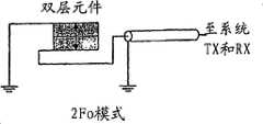
[0046]在图1中示出的实施例中,无源切换电路26、28、30将系统通道24连接至该元件12使得顶层和底层14、16二者响应于相同的发射波形。中心端子或电极20与该系统通道24和相关联的发射波束生成器通道连接。图3示出了作为断路起作用的无源限流电路(无源开关26)和作为闭合电路起作用的无源限压电路(无源开关28、30)。源自发射波束生成器的高压信号导致了图3的该配置。当相对于接触顶部和底部端子(电极18、22)二者的公共返回通路(common return path)驱动或感测该中心端子(电极20)时,该元件的两个层14、16由于相反的极化而同相地动作。该元件12以基本发射频率fo或以具有在第二谐波频率2fo或相关联的频带处的抑制响应的相关联的频带进行响应。[0046] In the embodiment shown in FIG. 1,
[0047]无源切换电路26、28、30将该系统通道24连接至该元件12使得由顶层和底层14、16二者产生的信号被提供给接收波束生成器通道。该接收波束生成器通道跨层14、16二者来连接。底层16的外侧电极22与该系统通道24和相关联的接收波束生成器通道连接。图4示出了作为闭合电路起作用的无源限流电路(无源开关26)和作为断路起作用的无源限压电路(无源开关28、40)。响应于所发射的声能由层14、16产生的低电压接收信号导致了图4的该配置。当直接跨整个厚度(即,两层)驱动或感测该元件12时,两个堆叠的层14、16的相反极化导致了对信号的不同相求和。该元件12以二次谐波频率2fo或基频的频带或具有在基频fo或频带处的抑制响应的频带进行强响应。[0047]
[0048]无源切换在发射与接收操作期间提供自动切换。对于谐波操作,该系统10以基本fo模式自动驱动该元件12并且响应地以谐波2fo模式感测该元件12。其它布置也是可能的,比如具有更多的层和/或不同的极化。发射操作可以处于基频,而接收操作处于分数谐波,例如1/2谐波。[0048] Passive switching provides automatic switching during transmit and receive operations. For harmonic operation, the
[0049]可以使用无源切换电路26、28、30的其它布置,例如连接至不同的电极18、20、22,连接至多于一个的电极18、20、22,并联和/或串联连接,或接地。使用了一个无源限流电路,但可以不使用或使用更多的无源限流电路。使用了两个无源限压电路,但可以不使用、使用更少或使用更多的无源限压电路。[0049] Other arrangements of
[0050]图5示出了采用三个无源限压电路(无源开关28、30和52)的另一实施例。变压器50连接在无源开关26和电极22之间。该变压器50具有1∶1绕线比。接收通路的有效阻抗可以通过在任一方向远离1∶1改变该绕线比而被改变。该变压器50的次级绕组的一端与电极22连接而另一端与电极18连接。该附加的无源限压电路(无源开关52)将该电极18和该变压器50与本地地连接。[0050] FIG. 5 shows another embodiment using three passive voltage limiting circuits (
[0051]图1的系统10在图4中示出的谐波操作期间为该元件12的层14、16提供了部分不对称的地。无源限压电路(无源开关30)导致采用比上层14小约0.6V的电压来驱动下层16。图5提供一种更平衡的布置。层14、16均遭受由无源限压电路(无源开关30、52)引起的与地的相同电压偏移。可以提供发射信号中的改善的二次谐波抑制(secondharmonic rejection)。[0051] The
[0052]图1和5的实施例都免于有源切换。在可替换的实施例中,无源开关中的一个或多个被替换为有源开关。在其它实施例中,提供有源开关。[0052] The embodiments of Figures 1 and 5 are both free from active switching. In an alternative embodiment, one or more of the passive switches are replaced with active switches. In other embodiments, active switches are provided.
[0053]图6示出了采用有源切换和无源切换的实施例。有源开关60、62是FET开关,但可以使用其它晶体管。开关60是单刀单掷开关。开关62是双刀开关,例如两个单刀单掷开关的布置。[0053] FIG. 6 shows an embodiment employing active switching and passive switching. The active switches 60, 62 are FET switches, but other transistors could be used.
[0054]有源开关60、62对信号通路再分配并且提供谐波和基本成像模式二者。当开关60、62处于位置A时,元件12以谐波模式操作(例如,以fo发射和以2fo接收)。当开关60、62处于位置B时,该元件12对于发射和接收二者以基本模式(fundamental mode)操作。开关60、62可以慢慢调整。因为开关60、62在设置成像模式之后是静止的,开关调整可能不改变元件12的性能。对于多模式情况来说,例如在与谐波模式成像交叉的基本模式中的多普勒成像,可以使用快速模式改变。调整时间和功率耗散可以改变性能或者足够的有源开关可以被识别。[0054]
[0055]在其它实施例中,基本上在相同方向上对两个层极化。无源切换构成了至两个层的串联电连接以便发射并且构成了至两个层的并联电连接以便接收。在实现基本模式和谐波模式操作中存在极化方向对电连接的二重性(duality)。[0055] In other embodiments, both layers are polarized in substantially the same direction. Passive switching constitutes a series electrical connection to the two layers for transmission and a parallel electrical connection to the two layers for reception. There is a duality of polarization direction versus electrical connection in achieving fundamental mode and harmonic mode operation.
[0056]图9示出了使用单独的发射和接收通道的实施例,用于采用多层元件来操作。该超声系统具有:a)MN个独立通道(其中M是层数而N是元件数),b)相互独立的用于发射的MN/2个通道和用于接收的MN/2个通道(M是偶数),或c)可以在接收和发射事件之间快速从一半的MN输入切换到另一半的多路复用器。每个元件有大于两个的层的换能器可以使用仅具有2N个系统通道的该配置。[0056] FIG. 9 shows an embodiment using separate transmit and receive channels for operation with multilayer components. The ultrasound system has: a) MN independent channels (where M is the number of layers and N is the number of elements), b) MN/2 channels for transmitting and MN/2 channels for receiving (M is even), or c) a multiplexer that can quickly switch from half of the MN inputs to the other half between receive and transmit events. Transducers with more than two layers per element can use this configuration with only 2N system channels.
[0057]可以通过具有更多数目的通道来提供更少的无源切换装置。可选的有源开关处在位置A用于谐波模式操作或处在位置B用于基本模式操作。基于无源开关Z1来自动设置至双层元件的两个层的发射和接收信号的相位。在基本模式中,上面的系统通道用于发射和接收二者。在另一个实施例中,在相同方向上对层14、16极化,并且发射(TX)通道与顶层14的顶部电极18或底层16的底部电极22连接。[0057] Fewer passive switching devices can be provided by having a greater number of channels. The optional active switch is in position A for harmonic mode operation or in position B for fundamental mode operation. The phase of the transmit and receive signals to the two layers of the bilayer element is automatically set based on the passive switch Z1. In basic mode, the upper system channels are used for both transmit and receive. In another embodiment, the
[0058]图7示出了使用无源切换的系统10′的另一实施例。无源开关26、28、30操作来控制如以上对图1所论述的基本响应和谐波响应,而且根据发射与接收操作调谐元件12。在其它实施例中,无源切换在没有基本响应和谐波响应改变的情况下提供调谐。[0058] FIG. 7 shows another embodiment of a system 10' using passive switching. The passive switches 26, 28, 30 operate to control the fundamental and harmonic responses as discussed above with respect to FIG. 1, and operate the
[0059]该系统10′具有调谐电路70、72。调谐电路70、72是电阻器,电容器、电感器,或其组合。如所示,调谐电路70、72分别具有由单个电感器提供的不同的阻抗。可以提供不止一种类型的调谐部件,例如多个电感器、电容器和/或电阻器的并联或串联连接。可以使用任何现在已知的或者后来开发的调谐电路70、72。该调谐提供阻抗匹配。[0059] The system 10' has
[0060]无源开关26、28、30中的一个或多个与调谐电路70、72中的一个或多个连接。如图7所示,一调谐电路70连接在元件12和一无源开关28之间。该无源开关28在操作期间基于操作的发射模式或者接收模式添加或去除调谐电路70。无源开关26的限压电路将调谐电路70切换进或出正被使用的通路。可以使用其它限压电路和调谐电路70的相关联位置。可替换地,可以采用无源开关28或不同类型无源切换的组合的限流电路来切换调谐电路70。[0060] One or more of the
[0061]另一调谐电路72与系统通道24连接,以便在发射和接收操作二者期间调谐。该另一调谐电路72处在换能器连接器或成像系统中。可替换地,该调谐电路72处在换能器探头中。[0061] Another
[0062]采用无源切换来分别地优化该元件12的发射和接收响应。针对发射和接收操作的不同调谐将波束生成器通道与不同的元件12阻抗响应相匹配。对发射和接收响应的优化采用不同的调谐电感器值。采用在图7中示出的无源切换,该元件12对于发射操作考虑12μH头部(head)或换能器调谐,对于接收操作考虑0μH头部或换能器调谐。[0062] Passive switching is employed to optimize the transmit and receive responses of the
[0063]图8示出了对于针对发射操作与针对接收操作来说不同调谐的无源切换的另一实施例。虽然采用谐波模式成像的无源切换来示出,但可以使用不具有无源切换和/或具有单层换能器材料的元件。诸如无源限流电路的无源开关80与调谐电路84(例如,电感器)串联。另一调谐电路82(例如,另一电感器)与该串联调谐电路84和无源开关80并联。[0063] FIG. 8 shows another embodiment for passive switching tuned differently for transmit operation than for receive operation. Although shown with passive switching for harmonic mode imaging, elements without passive switching and/or with a single layer of transducer material could be used. A
[0064]调谐电路82、84位于换能器连接器和/或成像系统中。可替换地,调谐电路82、84中的一个或两个处于换能器探头中。[0064]
[0065]无源开关80在发射操作期间断开或实际上是断路。发射通路仅具有调谐电路82(例如,12μH的电感器)。在接收操作期间采用小电流,该无源开关80实际上闭合或接通,以便接收通路基于并联的调谐电路82、84来考虑调谐(例如,并联的12μH和10.5μH相对于该元件12产生5.6μH)。可以提供其它电感器值、无源开关、无源开关的网络、调谐电路、调谐电路的组合、串联连接和/或并联连接。可以与任何换能器(不仅仅是双层装置)一起使用本调谐实施例和方法。[0065]
[0066]用于在超声和电能之间转换的方法采用无源切换。图1或4-8的实施例之一或无源开关的不同系统实现该方法。诸如无源电流和/或电压限制电路的无源开关根据信号的电压提供不同的发射和接收配置。对多层元件的换能器层的电气访问在并联和串联连接之间无源地切换。该换能器可以在没有发射与接收之间的有源开关控制的情况下以基本(f0)模式发射并且以谐波(例如,2f0)模式接收。[0066] The method for switching between ultrasound and electrical energy employs passive switching. One of the embodiments of Figures 1 or 4-8 or a different system of passive switches implements the method. Passive switches such as passive current and/or voltage limiting circuits provide different transmit and receive configurations depending on the voltage of the signal. Electrical access to the transducer layers of the multilayer element is passively switched between parallel and series connections. The transducer can transmit in fundamental (f0) mode and receive in harmonic (eg, 2f0) mode without active switch control between transmit and receive.
[0067]在一特定实例中,将发射波形应用于元件。该发射波形是具有任何周期数的单极、双极、正弦、方波或其它波形。由发射波束生成器在系统通道上或通过发射/接收开关输出波形来应用该波形。系统通道将该电波形传导到元件的一个或多个电极,例如将该波形传导到在两层换能器材料之间的中心元件。可以跨比全部层要少的层来应用该发射波形,应用于并联的层,或应用于串联的层。[0067] In a particular example, a transmit waveform is applied to a component. The transmit waveform is a unipolar, bipolar, sinusoidal, square or other waveform with any number of cycles. This waveform is applied by the transmit beamformer on the system channel or via the transmit/receive switch output waveform. A system channel conducts the electrical waveform to one or more electrodes of the element, for example to a central element between two layers of transducer material. The transmit waveform may be applied across fewer than all layers, to layers in parallel, or to layers in series.
[0068]发射波形具有相对高的电压振幅,例如正和/或负10伏特或更多的伏特(例如,100-200伏特)。可以使用更小的或更大的电压。[0068] The transmit waveform has a relatively high voltage amplitude, eg, plus and/or minus 10 volts or more (eg, 100-200 volts). Lesser or greater voltages can be used.
[0069]该发射波形具有所期望的频率或频带。例如,2MHz的中心频率配备有任何大小的频带,例如1或2MHz的频带。该中心频率和相应的带宽为基本发射频率和频带。[0069] The transmit waveform has a desired frequency or frequency band. For example, a center frequency of 2 MHz is provided with bands of any size, such as bands of 1 or 2 MHz. This center frequency and corresponding bandwidth is the fundamental transmit frequency and frequency band.
[0070]响应于发射波形,换能器材料产生声能。不同层的换能器材料有助于声能的产生。在给定的发射事件期间一个或多个元件产生声能。在元件之间采用相对定相和/或切趾(apodization),形成了一束或多束声能。[0070] In response to the transmit waveform, the transducer material generates acoustic energy. Different layers of transducer material contribute to the generation of sound energy. One or more elements generate acoustic energy during a given emission event. One or more beams of acoustic energy are formed using relative phasing and/or apodization between the elements.
[0071]诸如组织或流体的结构将一些声能反射回换能器元件。对于谐波成像来说,非线性传播和/或反射产生谐波信息。谐波信息被用于组织成像或造影剂成像之一。在组织成像中,在成像期(imaging session)期间不将附加的造影剂增加给目标。对于创建超声图象,仅仅依靠组织(包括血液或其它流体)的特性。典型地在离散成像期中为给定主体在给定时间传导医学超声成像。例如,成像期可能限于在1/4到1小时时期内对感兴趣的特定组织的超声患者检查,但是其它持续时间也是可能的。在这种情况下,在成像期期间的任何时间都不将造影剂引入该组织。组织谐波图像可以根据以谐波频率从组织产生的回波来提供尤其高的空间分辨率。特别地,在近场中往往可以存在较小的杂乱回波(clutter)。此外,与采用以第二谐波直接发射的信号形成的发射波束相比,因为采用基本频率产生发射波束,该发射波束的分布图可以较小地因特定水平的与组织相关的相位差而失真。[0071] Structures such as tissue or fluid reflect some acoustic energy back to the transducer element. For harmonic imaging, nonlinear propagation and/or reflections generate harmonic information. The harmonic information is used for one of tissue imaging or contrast agent imaging. In tissue imaging, no additional contrast agent is added to the target during an imaging session. For creating ultrasound images, only the properties of tissue (including blood or other fluids) are relied upon. Medical ultrasound imaging is typically conducted for a given subject at a given time in discrete imaging sessions. For example, an imaging session may be limited to an ultrasound patient examination of a particular tissue of interest over a 1/4 to 1 hour period, although other durations are possible. In this case, no contrast agent is introduced into the tissue at any time during the imaging session. Tissue harmonic images can provide particularly high spatial resolution based on echoes generated from tissue at harmonic frequencies. In particular, there may tend to be smaller clutters in the near field. Furthermore, since the transmit beam is generated using the fundamental frequency, the profile of the transmit beam may be less distorted by a certain level of tissue-related phase difference than a transmit beam formed using a signal transmitted directly at the second harmonic .
[0072]成像可以受助于造影剂的引入。在造影剂谐波成像中,多个公知的超声造影剂中的任何一个(例如微球体)被增加给目标或患者以便增强组织或流体的非线性响应。造影剂以处于基本频率的声穿透能量的谐波辐射超声能。可替换地,对基本频率处的信息感兴趣。[0072] Imaging may be aided by the introduction of a contrast agent. In contrast harmonic imaging, any of a number of well-known ultrasound contrast agents, such as microspheres, are added to a target or patient in order to enhance the non-linear response of tissue or fluid. The contrast agent radiates ultrasonic energy at harmonics of the insonification energy at the fundamental frequency. Alternatively, the information at the fundamental frequency is of interest.
[0073]由换能器元件将所反射的声能转换成电能。响应于应用发射波形和产生声音发射能量,由该元件来产生电接收波形。换能器材料层分别有助于接收波形的产生,或者单独的波形被电组合。例如,跨全部或部分串联的层产生接收波形。层的外侧电极与系统通道连接以便传导接收波形。在给定层的相反极化的情况下,串联连接以基本频带的谐波频带产生信息。还可以或可替换地以基本频带产生信息。[0073] The reflected acoustic energy is converted into electrical energy by the transducer element. An electrical receive waveform is generated by the element in response to applying the transmit waveform and generating acoustic transmit energy. The layers of transducer material contribute separately to the generation of the received waveform, or the separate waveforms are combined electrically. For example, a receive waveform is generated across all or part of the cascaded layers. The outer electrodes of the layers are connected to the system channels for conducting and receiving waveforms. The series connection produces information at harmonic frequency bands of the fundamental frequency band, given the opposite polarization of the layers. The information may also or alternatively be generated in the fundamental frequency band.
[0074]与发射波形相比,接收波形具有相对低的电压。例如,接收波形具有正和/或负10伏特或更小伏特的振幅。可以使用更高的或更低的电压。[0074] The receive waveform has a relatively low voltage compared to the transmit waveform. For example, the received waveform has an amplitude of plus and/or minus 10 volts or less. Higher or lower voltages can be used.
[0075]更高电压发射波形和更低电压接收波形沿相同的通道传送。发射和接收操作共享导体,例如共享同轴电缆。为发射和接收操作不同地使用该元件的层。[0075] The higher voltage transmit waveform and the lower voltage receive waveform are transmitted along the same channel. Transmit and receive operations share a conductor, such as a shared coaxial cable. The layers of this element are used differently for transmit and receive operations.
[0076]为了在共享通道时提供对层的不同的使用,而使用无源切换。无源开关在该元件中的换能器材料层的并联和串联连接之间进行改变。切换的发生与电压电平有关。对于高的电压来说限压电路无源地充当闭合电路,而对于较低的电压来说充当断路。对于高的电压来说限流电路无源地充当断路,而对于较低电压来说充当闭合电路。[0076] To provide different usage of layers when sharing channels, passive switching is used. A passive switch changes between parallel and series connection of the layers of transducer material in the element. Switching occurs in relation to voltage levels. The voltage limiting circuit acts passively as a closed circuit for high voltages and as an open circuit for lower voltages. The current limiting circuit passively acts as an open circuit for high voltages and as a closed circuit for lower voltages.
[0077]例如,较高电压发射波形穿过闭合开关到一个或多个电极(例如层间的中心电极),但被阻止穿过一个或多个开放的开关到一个或多个其它电极。较低电压接收波形从一个或多个不同的电极(例如一层的外部电极)穿过不同的闭合开关,但被阻止从其它电极穿过一个或多个不同的开关。采用二极管或其它电路执行限压,采用无源晶体管或其它电路执行限流。无源开关(例如限流电路和/或限压电路)的布置在用于发射波形的层并联连接和用于接收波形的层串联连接之间切换。在图1的实例实施例中,从通道到层之间的中心电极提供限压,从通道到在层之一上与中心电极相对的电极提供限流,从在另一层上与中心电极相对的另一电极到地提供限压。[0077] For example, a higher voltage transmit waveform passes through a closed switch to one or more electrodes (eg, a center electrode between layers), but is blocked from passing through one or more open switches to one or more other electrodes. Lower voltage receiving waveforms pass from one or more different electrodes (eg, outer electrodes of a layer) through different closed switches, but are blocked from other electrodes through one or more different switches. Voltage limiting is performed using diodes or other circuits, and current limiting is performed using passive transistors or other circuits. An arrangement of passive switches (eg, current limiting circuits and/or voltage limiting circuits) switches between parallel connection of layers for transmitting waveforms and series connection of layers for receiving waveforms. In the example embodiment of Figure 1, voltage limiting is provided from the channel to the center electrode between the layers, current limiting is provided from the channel to the electrode on one of the layers opposite the center electrode, and from the channel on the other layer opposite the center electrode. The other electrode to ground provides limiting voltage.
[0078]无源切换可以提供对层的不对称的或对称的(即,平衡的)接地。对于平衡接地来说,例如采用图5,变压器在发射波形的应用期间隔离了接地。提供对每个层至地的相同或类似的无源切换。[0078] Passive switching may provide asymmetric or symmetric (ie, balanced) grounding of the layers. For a balanced ground, for example using Figure 5, the transformer isolates the ground during the application of the transmit waveform. Provide the same or similar passive switching for each layer to ground.
[0079]还可以执行有源切换。在区域扫描期间重复地执行与电压电平有关的无源切换。发射与接收操作之间的每次转变产生了无源切换。诸如在交叉扫描之间或对于不同的总的成像模式(例如,B模式、造影剂模式、组织谐波模式、多普勒模式或其它成像模式)采用相同或不同的频率来执行有源切换。[0079] Active switching may also be performed. The voltage level dependent passive switching is repeatedly performed during the area scan. Every transition between transmit and receive operation creates a passive switch. Active switching is performed with the same or different frequencies, such as between cross-scans or for different overall imaging modes (eg, B-mode, contrast mode, tissue harmonic mode, Doppler mode, or other imaging modes).
[0080]有源开关重新布置或旁路(bypass)无源开关的配置。通过有源切换,可以控制无源开关的切换,在一模式中,无源切换或缺少无源切换规定以基本频率发射和接收。在由有源开关设置的另一模式中,无源切换规定以不同的频率发射和接收。可以在不同的无源切换配置之间选择有源切换,以便提供部件的不同组合或层的串联对并联连接。[0080] Configuration of active switch rearrangement or bypass of passive switches. By means of active switching, switching of passive switches can be controlled, in a mode where passive switching, or lack thereof, provides for transmission and reception at the fundamental frequency. In another mode set by an active switch, passive switching provides for transmission and reception at different frequencies. Active switching can be selected between different passive switching configurations to provide different combinations of components or series-to-parallel connections of layers.
[0081]无源切换可以可替换地或另外提供用于调谐超声元件的方法。通过根据应用发射波形和产生接收波形来进行无源切换,提供了不同的调谐。提供不同的调谐电路或调谐电路组合。在一个实施例中,无源切换断开一个或多个调谐电路。在其它实施例中,无源切换连接一个或多个调谐电路。可以为发射和接收操作二者连接一个或多个调谐电路。通过调谐电路的任何不同组合来提供不同的调谐。例如,将调谐电路切换进和切换出没有其他调谐电路或者具有其他调谐电路的连接。作为另一实例,为不同的模式提供不同的调谐电路或电路组合。模式与发射和接收操作相对应,其中无源切换与信号电压电平相关。[0081] Passive switching may alternatively or additionally provide a method for tuning the ultrasonic element. Different tunings are provided by passively switching the transmit waveform and generating the receive waveform according to the application. Different tuned circuits or combinations of tuned circuits are available. In one embodiment, passive switching disconnects one or more tuned circuits. In other embodiments, passive switching connects one or more tuned circuits. One or more tuned circuits may be connected for both transmit and receive operations. Different tunings are provided by any different combination of tuning circuits. For example, switching tuned circuits in and out of connections without or with other tuned circuits. As another example, different tuning circuits or combinations of circuits are provided for different modes. Modes correspond to transmit and receive operations where passive switching is related to the signal voltage level.
[0082]尽管参考各种实施例描述了本发明,应该理解的是在不脱离本发明范围的情况下可以进行许多改变和修改。因此,意在将以上详述的说明认为是例示性的而不是限制性的,并且应当理解,以下权利要求及其等效物意在限定本发明的精神和范围。[0082] While the invention has been described with reference to various embodiments, it should be understood that many changes and modifications can be made without departing from the scope of the invention. Accordingly, it is intended that the foregoing detailed description be considered as illustrative rather than restrictive, and it should be understood that the following claims and their equivalents are intended to define the spirit and scope of the invention.
Claims (30)
Translated fromChineseApplications Claiming Priority (3)
| Application Number | Priority Date | Filing Date | Title |
|---|---|---|---|
| US11/505,558 | 2006-08-16 | ||
| US11/505,558US8946972B2 (en) | 2006-08-16 | 2006-08-16 | Layer switching for an ultrasound transducer array |
| PCT/US2007/017922WO2008021325A2 (en) | 2006-08-16 | 2007-08-13 | Layer switching for an ultrasound transducer array |
Publications (2)
| Publication Number | Publication Date |
|---|---|
| CN101528364Atrue CN101528364A (en) | 2009-09-09 |
| CN101528364B CN101528364B (en) | 2013-11-13 |
Family
ID=38969484
Family Applications (1)
| Application Number | Title | Priority Date | Filing Date |
|---|---|---|---|
| CN2007800385661AActiveCN101528364B (en) | 2006-08-16 | 2007-08-13 | Layer switching for ultrasound transducer arrays |
Country Status (6)
| Country | Link |
|---|---|
| US (1) | US8946972B2 (en) |
| JP (1) | JP4991857B2 (en) |
| KR (1) | KR101142678B1 (en) |
| CN (1) | CN101528364B (en) |
| DE (1) | DE112007001920B4 (en) |
| WO (1) | WO2008021325A2 (en) |
Cited By (4)
| Publication number | Priority date | Publication date | Assignee | Title |
|---|---|---|---|---|
| CN103800035A (en)* | 2012-11-14 | 2014-05-21 | Ge医疗系统环球技术有限公司 | Ultrasonic probe and ultrasonic diagnostic apparatus |
| CN105592942A (en)* | 2013-10-03 | 2016-05-18 | 富士胶片戴麦提克斯公司 | Piezoelectric ultrasonic transducer array with switched operational modes |
| CN108144199A (en)* | 2017-12-22 | 2018-06-12 | 深圳先进技术研究院 | Device, method and system are motivated by ultrasound |
| US10586912B2 (en) | 2013-12-11 | 2020-03-10 | Fujifilm Dimatix, Inc. | Method for fabricating flexible micromachined transducer device |
Families Citing this family (12)
| Publication number | Priority date | Publication date | Assignee | Title |
|---|---|---|---|---|
| US7804228B2 (en)* | 2007-12-18 | 2010-09-28 | Boston Scientific Scimed, Inc. | Composite passive materials for ultrasound transducers |
| US20100204582A1 (en)* | 2009-02-12 | 2010-08-12 | Xuan-Ming Lu | Multidimensional, multilayer ultrasound transducer probe for medical ultrasound imaging |
| US8208346B2 (en)* | 2009-03-23 | 2012-06-26 | Liposonix, Inc. | Selectable tuning transformer |
| US8488813B2 (en)* | 2009-04-01 | 2013-07-16 | Avago Technologies General Ip (Singapore) Pte. Ltd. | Reconfigurable acoustic transducer device |
| US20110098573A1 (en)* | 2009-10-27 | 2011-04-28 | Boston Scientific Scimed, Inc. | Systems and methods for coupling a transducer to a control module of an intravascular ultrasound imaging system |
| US20130257552A1 (en)* | 2010-12-20 | 2013-10-03 | Yasuharu Onishi | Oscillator device and electronic instrument |
| DE102011076117B4 (en)* | 2011-05-19 | 2021-10-14 | Robert Bosch Gmbh | Ultrasonic measuring system and method for detecting an obstacle using ultrasound |
| JP6024519B2 (en)* | 2013-03-04 | 2016-11-16 | コニカミノルタ株式会社 | Ultrasonic diagnostic equipment |
| US9375200B2 (en)* | 2013-03-12 | 2016-06-28 | Siemens Medical Solutions Usa, Inc. | Ultrasound transducer with differential mode signaling |
| US9437802B2 (en) | 2013-08-21 | 2016-09-06 | Fujifilm Dimatix, Inc. | Multi-layered thin film piezoelectric devices and methods of making the same |
| CN110312477A (en)* | 2016-09-29 | 2019-10-08 | 精密成像有限公司 | Signal processing approach for ultrasound imaging apparatus |
| EP3482835A1 (en) | 2017-11-14 | 2019-05-15 | Koninklijke Philips N.V. | Capacitive micro-machined ultrasound transducer (cmut) devices and control methods |
Citations (4)
| Publication number | Priority date | Publication date | Assignee | Title |
|---|---|---|---|---|
| US5825117A (en)* | 1996-03-26 | 1998-10-20 | Hewlett-Packard Company | Second harmonic imaging transducers |
| US5957851A (en)* | 1996-06-10 | 1999-09-28 | Acuson Corporation | Extended bandwidth ultrasonic transducer |
| CN1426288A (en)* | 2000-02-23 | 2003-06-25 | 阿库森公司 | Ultrasound transducer system and method for harmonic imaging |
| US20050148879A1 (en)* | 2003-12-19 | 2005-07-07 | Siemens Medical Solutions Usa, Inc. | Mode dependent tunable transducers and methods of use |
Family Cites Families (12)
| Publication number | Priority date | Publication date | Assignee | Title |
|---|---|---|---|---|
| US3697862A (en)* | 1971-06-15 | 1972-10-10 | Hewlett Packard Co | Power supply having means for limiting load currents with both active and passive loads |
| US5410205A (en)* | 1993-02-11 | 1995-04-25 | Hewlett-Packard Company | Ultrasonic transducer having two or more resonance frequencies |
| US5675554A (en) | 1994-08-05 | 1997-10-07 | Acuson Corporation | Method and apparatus for transmit beamformer |
| US5685308A (en) | 1994-08-05 | 1997-11-11 | Acuson Corporation | Method and apparatus for receive beamformer system |
| US6005827A (en) | 1995-03-02 | 1999-12-21 | Acuson Corporation | Ultrasonic harmonic imaging system and method |
| US6104670A (en) | 1995-03-02 | 2000-08-15 | Acuson Corporation | Ultrasonic harmonic imaging system and method |
| US5608690A (en) | 1995-03-02 | 1997-03-04 | Acuson Corporation | Transmit beamformer with frequency dependent focus |
| US5608609A (en) | 1995-09-11 | 1997-03-04 | Lucent Technologies Inc. | Outdoor cabinet for electronic equipment |
| DE19836997B4 (en) | 1998-08-14 | 2004-03-25 | Siemens Ag | Transmission / reception circuit and transmission / reception method for a converter |
| CN1666568A (en)* | 2001-01-05 | 2005-09-07 | 比约恩·A·J·安杰尔森 | broadband transducer |
| US6761692B2 (en) | 2001-06-25 | 2004-07-13 | Eagle Ultrasound As | High frequency and multi frequency band ultrasound transducers based on ceramic films |
| US6673016B1 (en)* | 2002-02-14 | 2004-01-06 | Siemens Medical Solutions Usa, Inc. | Ultrasound selectable frequency response system and method for multi-layer transducers |
- 2006
- 2006-08-16USUS11/505,558patent/US8946972B2/enactiveActive
- 2007
- 2007-08-13KRKR1020097005418Apatent/KR101142678B1/enactiveActive
- 2007-08-13CNCN2007800385661Apatent/CN101528364B/enactiveActive
- 2007-08-13WOPCT/US2007/017922patent/WO2008021325A2/enactiveApplication Filing
- 2007-08-13JPJP2009524650Apatent/JP4991857B2/enactiveActive
- 2007-08-13DEDE112007001920.4Tpatent/DE112007001920B4/enactiveActive
Patent Citations (4)
| Publication number | Priority date | Publication date | Assignee | Title |
|---|---|---|---|---|
| US5825117A (en)* | 1996-03-26 | 1998-10-20 | Hewlett-Packard Company | Second harmonic imaging transducers |
| US5957851A (en)* | 1996-06-10 | 1999-09-28 | Acuson Corporation | Extended bandwidth ultrasonic transducer |
| CN1426288A (en)* | 2000-02-23 | 2003-06-25 | 阿库森公司 | Ultrasound transducer system and method for harmonic imaging |
| US20050148879A1 (en)* | 2003-12-19 | 2005-07-07 | Siemens Medical Solutions Usa, Inc. | Mode dependent tunable transducers and methods of use |
Cited By (5)
| Publication number | Priority date | Publication date | Assignee | Title |
|---|---|---|---|---|
| CN103800035A (en)* | 2012-11-14 | 2014-05-21 | Ge医疗系统环球技术有限公司 | Ultrasonic probe and ultrasonic diagnostic apparatus |
| CN105592942A (en)* | 2013-10-03 | 2016-05-18 | 富士胶片戴麦提克斯公司 | Piezoelectric ultrasonic transducer array with switched operational modes |
| CN105592942B (en)* | 2013-10-03 | 2018-07-06 | 富士胶片戴麦提克斯公司 | Piezoelectric ultrasonic transducer array with switching operation modes |
| US10586912B2 (en) | 2013-12-11 | 2020-03-10 | Fujifilm Dimatix, Inc. | Method for fabricating flexible micromachined transducer device |
| CN108144199A (en)* | 2017-12-22 | 2018-06-12 | 深圳先进技术研究院 | Device, method and system are motivated by ultrasound |
Also Published As
| Publication number | Publication date |
|---|---|
| DE112007001920B4 (en) | 2016-01-28 |
| KR20090042319A (en) | 2009-04-29 |
| JP2010500850A (en) | 2010-01-07 |
| JP4991857B2 (en) | 2012-08-01 |
| US20080042519A1 (en) | 2008-02-21 |
| KR101142678B1 (en) | 2012-05-11 |
| CN101528364B (en) | 2013-11-13 |
| WO2008021325A2 (en) | 2008-02-21 |
| DE112007001920T5 (en) | 2009-06-25 |
| US8946972B2 (en) | 2015-02-03 |
| WO2008021325A3 (en) | 2009-02-26 |
Similar Documents
| Publication | Publication Date | Title |
|---|---|---|
| CN101528364A (en) | Layer switching for ultrasound transducer arrays | |
| US11712222B2 (en) | Configurable ultrasonic imager | |
| JP5204116B2 (en) | Enhanced ultrasound imaging probe using a flexural mode piezoelectric transducer | |
| JP5679983B2 (en) | Front-end circuit for ultrasonic transducer probe | |
| US8182428B2 (en) | Dual frequency band ultrasound transducer arrays | |
| US20100204582A1 (en) | Multidimensional, multilayer ultrasound transducer probe for medical ultrasound imaging | |
| EP3787807B1 (en) | Ultrasound transducer | |
| US6673016B1 (en) | Ultrasound selectable frequency response system and method for multi-layer transducers | |
| US10952706B2 (en) | Ultrasound systems with microbeamformers for different transducer arrays | |
| US7713199B2 (en) | Medical diagnostic ultrasound transducer system for harmonics | |
| JPH1023598A (en) | Piezoelectric conversion device | |
| EP1396172A2 (en) | Wideband transducer | |
| EP2268419A1 (en) | Multiple frequency band acoustic transducer arrays | |
| KR20210053296A (en) | Ultrasound Imaging and Energy Delivery Apparatus and Method | |
| US10152963B2 (en) | Ultrasound transducer with differential mode signaling | |
| JP2003531649A (en) | Ultrasonic transducer system and method for harmonic imaging | |
| WO2015145296A1 (en) | Ultrasound probes and systems having pin-pmn-pt, a dematching layer, and improved thermally conductive backing materials | |
| JP2012143615A (en) | Enhanced ultrasound image diagnostic probe using flexure mode piezoelectric transducer | |
| Simpson | CMOS-integrated array transducers for high-frequency ultrasonic imaging | |
| Lu | Comprehensive design considerations for 2D matrix arrays |
Legal Events
| Date | Code | Title | Description |
|---|---|---|---|
| C06 | Publication | ||
| PB01 | Publication | ||
| C10 | Entry into substantive examination | ||
| SE01 | Entry into force of request for substantive examination | ||
| C14 | Grant of patent or utility model | ||
| GR01 | Patent grant |