CN101526709A - Liquid crystal display divice - Google Patents
Liquid crystal display diviceDownload PDFInfo
- Publication number
- CN101526709A CN101526709ACN200910126641ACN200910126641ACN101526709ACN 101526709 ACN101526709 ACN 101526709ACN 200910126641 ACN200910126641 ACN 200910126641ACN 200910126641 ACN200910126641 ACN 200910126641ACN 101526709 ACN101526709 ACN 101526709A
- Authority
- CN
- China
- Prior art keywords
- layer
- tft
- mentioned
- poly
- liquid crystal
- Prior art date
- Legal status (The legal status is an assumption and is not a legal conclusion. Google has not performed a legal analysis and makes no representation as to the accuracy of the status listed.)
- Granted
Links
Images


Classifications
- G—PHYSICS
- G02—OPTICS
- G02F—OPTICAL DEVICES OR ARRANGEMENTS FOR THE CONTROL OF LIGHT BY MODIFICATION OF THE OPTICAL PROPERTIES OF THE MEDIA OF THE ELEMENTS INVOLVED THEREIN; NON-LINEAR OPTICS; FREQUENCY-CHANGING OF LIGHT; OPTICAL LOGIC ELEMENTS; OPTICAL ANALOGUE/DIGITAL CONVERTERS
- G02F1/00—Devices or arrangements for the control of the intensity, colour, phase, polarisation or direction of light arriving from an independent light source, e.g. switching, gating or modulating; Non-linear optics
- G02F1/01—Devices or arrangements for the control of the intensity, colour, phase, polarisation or direction of light arriving from an independent light source, e.g. switching, gating or modulating; Non-linear optics for the control of the intensity, phase, polarisation or colour
- G02F1/13—Devices or arrangements for the control of the intensity, colour, phase, polarisation or direction of light arriving from an independent light source, e.g. switching, gating or modulating; Non-linear optics for the control of the intensity, phase, polarisation or colour based on liquid crystals, e.g. single liquid crystal display cells
- G02F1/1303—Apparatus specially adapted to the manufacture of LCDs
- H—ELECTRICITY
- H10—SEMICONDUCTOR DEVICES; ELECTRIC SOLID-STATE DEVICES NOT OTHERWISE PROVIDED FOR
- H10D—INORGANIC ELECTRIC SEMICONDUCTOR DEVICES
- H10D30/00—Field-effect transistors [FET]
- H10D30/01—Manufacture or treatment
- H10D30/021—Manufacture or treatment of FETs having insulated gates [IGFET]
- H10D30/031—Manufacture or treatment of FETs having insulated gates [IGFET] of thin-film transistors [TFT]
- H10D30/0312—Manufacture or treatment of FETs having insulated gates [IGFET] of thin-film transistors [TFT] characterised by the gate electrodes
- H10D30/0316—Manufacture or treatment of FETs having insulated gates [IGFET] of thin-film transistors [TFT] characterised by the gate electrodes of lateral bottom-gate TFTs comprising only a single gate
- H—ELECTRICITY
- H10—SEMICONDUCTOR DEVICES; ELECTRIC SOLID-STATE DEVICES NOT OTHERWISE PROVIDED FOR
- H10D—INORGANIC ELECTRIC SEMICONDUCTOR DEVICES
- H10D30/00—Field-effect transistors [FET]
- H10D30/01—Manufacture or treatment
- H10D30/021—Manufacture or treatment of FETs having insulated gates [IGFET]
- H10D30/031—Manufacture or treatment of FETs having insulated gates [IGFET] of thin-film transistors [TFT]
- H10D30/0321—Manufacture or treatment of FETs having insulated gates [IGFET] of thin-film transistors [TFT] comprising silicon, e.g. amorphous silicon or polysilicon
- H—ELECTRICITY
- H10—SEMICONDUCTOR DEVICES; ELECTRIC SOLID-STATE DEVICES NOT OTHERWISE PROVIDED FOR
- H10D—INORGANIC ELECTRIC SEMICONDUCTOR DEVICES
- H10D30/00—Field-effect transistors [FET]
- H10D30/60—Insulated-gate field-effect transistors [IGFET]
- H10D30/67—Thin-film transistors [TFT]
- H10D30/6704—Thin-film transistors [TFT] having supplementary regions or layers in the thin films or in the insulated bulk substrates for controlling properties of the device
- H10D30/6706—Thin-film transistors [TFT] having supplementary regions or layers in the thin films or in the insulated bulk substrates for controlling properties of the device for preventing leakage current
- H—ELECTRICITY
- H10—SEMICONDUCTOR DEVICES; ELECTRIC SOLID-STATE DEVICES NOT OTHERWISE PROVIDED FOR
- H10D—INORGANIC ELECTRIC SEMICONDUCTOR DEVICES
- H10D86/00—Integrated devices formed in or on insulating or conducting substrates, e.g. formed in silicon-on-insulator [SOI] substrates or on stainless steel or glass substrates
- H10D86/01—Manufacture or treatment
- H10D86/021—Manufacture or treatment of multiple TFTs
- H10D86/0231—Manufacture or treatment of multiple TFTs using masks, e.g. half-tone masks
- H—ELECTRICITY
- H10—SEMICONDUCTOR DEVICES; ELECTRIC SOLID-STATE DEVICES NOT OTHERWISE PROVIDED FOR
- H10D—INORGANIC ELECTRIC SEMICONDUCTOR DEVICES
- H10D86/00—Integrated devices formed in or on insulating or conducting substrates, e.g. formed in silicon-on-insulator [SOI] substrates or on stainless steel or glass substrates
- H10D86/40—Integrated devices formed in or on insulating or conducting substrates, e.g. formed in silicon-on-insulator [SOI] substrates or on stainless steel or glass substrates characterised by multiple TFTs
- H10D86/60—Integrated devices formed in or on insulating or conducting substrates, e.g. formed in silicon-on-insulator [SOI] substrates or on stainless steel or glass substrates characterised by multiple TFTs wherein the TFTs are in active matrices
- G—PHYSICS
- G02—OPTICS
- G02F—OPTICAL DEVICES OR ARRANGEMENTS FOR THE CONTROL OF LIGHT BY MODIFICATION OF THE OPTICAL PROPERTIES OF THE MEDIA OF THE ELEMENTS INVOLVED THEREIN; NON-LINEAR OPTICS; FREQUENCY-CHANGING OF LIGHT; OPTICAL LOGIC ELEMENTS; OPTICAL ANALOGUE/DIGITAL CONVERTERS
- G02F1/00—Devices or arrangements for the control of the intensity, colour, phase, polarisation or direction of light arriving from an independent light source, e.g. switching, gating or modulating; Non-linear optics
- G02F1/01—Devices or arrangements for the control of the intensity, colour, phase, polarisation or direction of light arriving from an independent light source, e.g. switching, gating or modulating; Non-linear optics for the control of the intensity, phase, polarisation or colour
- G02F1/13—Devices or arrangements for the control of the intensity, colour, phase, polarisation or direction of light arriving from an independent light source, e.g. switching, gating or modulating; Non-linear optics for the control of the intensity, phase, polarisation or colour based on liquid crystals, e.g. single liquid crystal display cells
- G02F1/133—Constructional arrangements; Operation of liquid crystal cells; Circuit arrangements
- G02F1/136—Liquid crystal cells structurally associated with a semi-conducting layer or substrate, e.g. cells forming part of an integrated circuit
- G02F1/1362—Active matrix addressed cells
- G02F1/1368—Active matrix addressed cells in which the switching element is a three-electrode device
- G—PHYSICS
- G02—OPTICS
- G02F—OPTICAL DEVICES OR ARRANGEMENTS FOR THE CONTROL OF LIGHT BY MODIFICATION OF THE OPTICAL PROPERTIES OF THE MEDIA OF THE ELEMENTS INVOLVED THEREIN; NON-LINEAR OPTICS; FREQUENCY-CHANGING OF LIGHT; OPTICAL LOGIC ELEMENTS; OPTICAL ANALOGUE/DIGITAL CONVERTERS
- G02F2202/00—Materials and properties
- G02F2202/10—Materials and properties semiconductor
- G02F2202/103—Materials and properties semiconductor a-Si
- G—PHYSICS
- G02—OPTICS
- G02F—OPTICAL DEVICES OR ARRANGEMENTS FOR THE CONTROL OF LIGHT BY MODIFICATION OF THE OPTICAL PROPERTIES OF THE MEDIA OF THE ELEMENTS INVOLVED THEREIN; NON-LINEAR OPTICS; FREQUENCY-CHANGING OF LIGHT; OPTICAL LOGIC ELEMENTS; OPTICAL ANALOGUE/DIGITAL CONVERTERS
- G02F2202/00—Materials and properties
- G02F2202/10—Materials and properties semiconductor
- G02F2202/104—Materials and properties semiconductor poly-Si
Landscapes
- Physics & Mathematics (AREA)
- Nonlinear Science (AREA)
- Engineering & Computer Science (AREA)
- Manufacturing & Machinery (AREA)
- Chemical & Material Sciences (AREA)
- Crystallography & Structural Chemistry (AREA)
- General Physics & Mathematics (AREA)
- Optics & Photonics (AREA)
- Liquid Crystal (AREA)
- Thin Film Transistor (AREA)
Abstract
Translated fromChinese
Description
Translated fromChinese技术领域technical field
本发明涉及显示装置,尤其涉及在显示区域上具有将TFT用于进行开关的像素且在显示区域的周边形成有由使用了poly-Si的TFT构成的驱动电路的液晶显示装置。The present invention relates to a display device, and more particularly, to a liquid crystal display device having pixels using TFTs for switching in a display region and a driver circuit composed of TFTs using poly-Si formed around the display region.
背景技术Background technique
在液晶显示装置中,TFT基板与滤色片基板相对置,在TFT基板与滤色片基板之间夹持有液晶,其中,在TFT基板上呈矩阵状形成有像素电极和薄膜晶体管(TFT)等,在滤色片基板的与像素电极对应的位置上形成有滤色片等。In a liquid crystal display device, a TFT substrate is opposed to a color filter substrate, and a liquid crystal is sandwiched between the TFT substrate and the color filter substrate. Pixel electrodes and thin-film transistors (TFTs) are formed in a matrix on the TFT substrate. etc., color filters and the like are formed on the color filter substrate at positions corresponding to the pixel electrodes.
在TFT基板上存在纵向延伸且横向排列的数据线和、横向延伸且纵向排列的扫描线,在由数据线和扫描线所包围的区域上形成有像素。像素主要构成有像素电极和作为开关元件的薄膜晶体管(TFT)。利用这样呈矩阵状形成的多个像素来形成显示区域。On the TFT substrate there are data lines extending vertically and arranged horizontally and scanning lines extending horizontally and arranged vertically, and pixels are formed on the area surrounded by the data lines and the scanning lines. A pixel is mainly composed of a pixel electrode and a thin film transistor (TFT) as a switching element. A display area is formed by a plurality of pixels formed in a matrix in this way.
在显示区域的外侧设置有驱动扫描线的扫描线驱动电路、驱动数据线的数据线驱动电路。以往,扫描线驱动电路和数据线驱动电路外设有IC驱动器。该IC驱动器有时也被通过载带(tape carrier)等而连接在TFT基板上,有时也是IC驱动器被直接贴装(chip on)在TFT基板上。A scanning line driving circuit for driving the scanning lines and a data line driving circuit for driving the data lines are arranged outside the display area. Conventionally, an IC driver is provided externally to the scanning line driving circuit and the data line driving circuit. The IC driver is sometimes connected to the TFT substrate through a tape carrier or the like, and sometimes the IC driver is directly mounted (chip on) on the TFT substrate.
另一方面,从确保显示区域并要减小显示装置整体这样的要求等考虑,开发了在显示区域周边利用TFT形成驱动电路的技术。在这种显示装置中,形成在显示区域中的TFT将a-Si使用于沟道部,形成在驱动电路部的TFT将poly-Si使用于沟道部。即,在显示区域中使用漏电流较小的a-Si,在驱动电路部中使用电子迁移率较大的poly-Si。On the other hand, in view of the need to secure a display area and reduce the size of the entire display device, a technique of forming a driver circuit using TFTs around the display area has been developed. In such a display device, a-Si is used for a channel portion of a TFT formed in a display region, and poly-Si is used for a channel portion of a TFT formed in a driver circuit portion. That is, a-Si having low leakage current is used in the display region, and poly-Si having high electron mobility is used in the driving circuit portion.
一般而言,在使用了a-Si的TFT中采用底栅结构。在使用了poly-Si的TFT中采用顶栅结构。但是,在一块基板上形成结构不同的TFT会使制造工序变得复杂。In general, a bottom gate structure is adopted for a TFT using a-Si. A top-gate structure is adopted in a TFT using poly-Si. However, forming TFTs with different structures on one substrate complicates the manufacturing process.
“专利文献1”记载了为了防止工序变得复杂,在使用了poly-Si的TFT中也采用底栅型的结构。该结构在形成于栅电极之上的栅极绝缘膜之上,首先形成成为沟道的poly-Si层,在其上形成a-Si层。在a-Si之上形成n+层的接触层,在其上形成源/漏电极(SD电极)。通过使将poly-Si用于沟道的TFT成为这样的结构,与将a-Si用于沟道的TFT相同的工序变多,从而使工序简化。"Patent Document 1" describes that a TFT using poly-Si also adopts a bottom-gate structure in order to prevent the process from becoming complicated. In this structure, a poly-Si layer to be a channel is first formed on a gate insulating film formed on a gate electrode, and an a-Si layer is formed thereon. A contact layer of an n+ layer is formed over the a-Si, and source/drain electrodes (SD electrodes) are formed thereon. Such a structure of a TFT using poly-Si for a channel increases the number of steps similar to that of a TFT using a-Si for a channel, thereby simplifying the process.
专利文献1:日本特开平5-55570号公报Patent Document 1: Japanese Patent Application Laid-Open No. 5-55570
发明内容Contents of the invention
在“专利文献1”记载的技术中,在形成于栅电极103之上的栅极绝缘层之上形成poly-Si层,在其上形成a-Si层,在其上形成n+层来取得接触。该结构在晶体管导通(ON)时,在迁移率较大的poly-Si层中流过导通电流。但是,使晶体管截止(OFF)时,产生漏电流的问题。In the technique described in "Patent Document 1", a poly-Si layer is formed on the gate insulating layer formed on the
图15是与“专利文献1”记载的相同的具有poly-Si沟道的TFT的结构。图15的(a)是俯视图,图15的(b)是图15的(a)的A-A线剖视图。在图15的(a)中,在栅电极103之上隔着栅极绝缘膜104而依次层叠有poly-Si层107、a-Si层108。在a-Si层108之上隔着n+Si层109而形成有SD电极113。FIG. 15 shows the structure of a TFT having a poly-Si channel similar to that described in "Patent Document 1". (a) of FIG. 15 is a plan view, and (b) of FIG. 15 is a sectional view taken along line A-A of (a) of FIG. 15 . In (a) of FIG. 15 , a poly-
图15的(b)是图15的(a)的详细剖视图。在图15的(b)中,在基底膜102之上形成有栅电极103,覆盖栅电极103而形成有栅极绝缘膜104。在栅极绝缘膜104之上形成有poly-Si层107,在其上形成有a-Si层108。在a-Si层108之上形成有n+Si层109。a-Si层108与n+Si层109使用相同的掩模来进行光刻,因此平面为相同的形状。在n+Si层109之上形成有SD电极113。SD电极113用由Mo构成的屏蔽金属层110、Al层111、由Mo构成的金属盖层112来形成。(b) of FIG. 15 is a detailed sectional view of (a) of FIG. 15 . In (b) of FIG. 15 , a
在图15那样的结构中,当在栅电极103上施加正电压来在TFT中流过导通电流时,能够使其作为TFT来工作。但是,当在栅电极103上施加零电压或负电压来使TFT为截止时,发现TFT不会截止这样的现象。这样将不具有TFT的作为开关元件的作用。研究认为这是由如下那样的原因所引起的。In the structure shown in FIG. 15 , when a positive voltage is applied to the
在图15的(b)中,当在栅电极103上施加负电压时,在poly-Si层107中感应出空穴。在poly-Si层107与SD电极113的屏蔽金属层110之间没有电位势垒。因此,基于空穴的电流照样流入SD电极113,所以TFT不会截止。In (b) of FIG. 15 , when a negative voltage is applied to the
图16是解决了这样的问题的TFT的剖视图。在图16中,在栅电极103之上隔着栅极绝缘膜104而形成有poly-Si层107和a-Si层108。a-Si层108形成沟道蚀刻部114,膜厚变小。覆盖沟道蚀刻部114和TFT整体而形成有基于SiN的钝化膜116。图17的特征在于:n+Si层109不仅覆盖在a-Si层108之上,还覆盖a-Si层108和poly-Si层107的侧部。通过采用这样的结构,在a-Si层108以及poly-Si层107与SD电极113之间形成n+Si层109,由此形成耗尽层,防止空穴通过。因此,能够防止截止电流的增加。FIG. 16 is a cross-sectional view of a TFT that solves such a problem. In FIG. 16 , poly-
但是,在图16所示那样的结构中,能够防止截止电流的增加,但存在无法获得足够的导通电流这样的问题。即,导通电流在迁移率较大的poly-Si层中流过。然而,poly-Si层与SD电极仅在poly-Si层的侧面接触。poly-Si层的厚度较薄,大约为50nm。因此,产生如下现象:SD电极与poly-Si层的接触电阻变大,无法获得足够的导通电流。However, in the configuration shown in FIG. 16 , an increase in the off-current can be prevented, but there is a problem that a sufficient on-current cannot be obtained. That is, the on-current flows through the poly-Si layer having high mobility. However, the poly-Si layer is in contact with the SD electrode only at the side of the poly-Si layer. The thickness of the poly-Si layer is relatively thin, about 50nm. Therefore, a phenomenon occurs in which the contact resistance between the SD electrode and the poly-Si layer becomes large, and a sufficient on-current cannot be obtained.
为了增大导通电流,需要增加poly-Si层与SD层的接触面积。为此,除去图17等所示的a-Si层即可。这样,能够增加poly-Si层与SD电极的接触面积。但是,当除去a-Si层时,变得无法取得图16所示的沟道蚀刻层114。即,poly-Si层的厚度为50nm,在该厚度范围内形成沟道蚀刻层是非常困难的。In order to increase the on-current, it is necessary to increase the contact area between the poly-Si layer and the SD layer. For this purpose, the a-Si layer shown in FIG. 17 and the like may be removed. In this way, the contact area between the poly-Si layer and the SD electrode can be increased. However, when the a-Si layer is removed, the
为了不形成沟道蚀刻层114而使TFT的工作稳定,形成后述的沟道截断环(channel stopper)即可。但是,形成沟道截断环、且形成poly-Si层与SD电极的面接触会增加光刻步骤,因此制造成本增加。In order to stabilize the operation of the TFT without forming the
本发明的课题在于:在底栅型poly-Si TFT中,实现能够抑制制造成本的增加的同时确保足够的导通电流的结构。The object of the present invention is to realize a structure capable of securing a sufficient on-current while suppressing an increase in manufacturing cost in a bottom-gate poly-Si TFT.
本发明是克服上述课题的发明,在底栅型、且将poly-Si层用于半导体层的TFT中,在poly-Si层之上形成沟道截断环,在比沟道截断环的端部更靠外的一侧形成poly-Si层的端部,由此使其与n+Si层以及源/漏电极的接触面积增加。为了实现该结构,通过湿法蚀刻来加工沟道截断环层,以干法蚀刻来加工poly-Si层。使用湿法蚀刻来侧面蚀刻沟道截断环,由此通过一次光刻工序来实现上述结构。具体方案如下。The present invention is an invention for overcoming the above-mentioned problems. In a bottom-gate type TFT using a poly-Si layer as a semiconductor layer, a channel stopper ring is formed on the poly-Si layer, and a channel stopper ring is formed at the end of the channel stopper ring. The more outer side forms the end of the poly-Si layer, thereby increasing its contact area with the n+Si layer and source/drain electrodes. To realize this structure, the channel stop ring layer is processed by wet etching and the poly-Si layer is processed by dry etching. The channel stop ring is laterally etched using wet etching, thereby achieving the above structure in one photolithography process. The specific plan is as follows.
(1)一种液晶显示装置,该装置形成有呈矩阵状形成了像素电极和TFT的显示区域、和在上述显示区域的周边包含TFT的驱动电路,其特征在于:上述TFT的结构为,覆盖栅电极而形成有栅极绝缘膜,在上述栅极绝缘膜之上形成有poly-Si层,在上述poly-Si层之上形成有沟道截断环层,覆盖上述沟道截断环层和上述poly-Si层的一部分而形成有n+Si层和源/漏电极,其中,上述沟道截断环层通过湿法蚀刻来进行加工,上述poly-Si层通过干法蚀刻来进行加工,由上述干法蚀刻所加工的上述poly-Si层的端部存在于比由上述湿法蚀刻所加工的沟道截断环的端部更靠外的一侧。(1) A liquid crystal display device having a display area in which pixel electrodes and TFTs are formed in a matrix, and a drive circuit including TFTs around the display area, wherein the TFT has a structure covering A gate insulating film is formed on the gate electrode, a poly-Si layer is formed on the above-mentioned gate insulating film, and a channel stopper ring layer is formed on the above-mentioned poly-Si layer, covering the above-mentioned channel stopper ring layer and the above-mentioned The n+Si layer and the source/drain electrodes are formed by forming a part of the poly-Si layer, wherein the channel stop ring layer is processed by wet etching, and the poly-Si layer is processed by dry etching. The end of the poly-Si layer processed by dry etching exists on the outer side than the end of the trench stopper ring processed by the wet etching.
(2)在(1)所述的液晶显示装置中,上述n+Si层通过干法蚀刻来进行加工。(2) In the liquid crystal display device described in (1), the n+Si layer is processed by dry etching.
(3)一种液晶显示装置,该装置形成有呈矩阵状形成了像素电极和TFT的显示区域、和在上述显示区域的周边包含TFT的驱动电路,其特征在于:上述TFT覆盖栅电极而形成有栅极绝缘膜,在上述栅极绝缘膜之上形成有poly-Si层,在上述poly-Si层的主面之上除了周边部而形成有沟道截断环层,n+Si层接触上述poly-Si层的主面的周边部,覆盖上述n+Si层而形成有源/漏电极。(3) A liquid crystal display device having a display region in which pixel electrodes and TFTs are formed in a matrix, and a drive circuit including TFTs around the display region, wherein the TFT is formed to cover the gate electrode There is a gate insulating film, a poly-Si layer is formed on the gate insulating film, a channel stop ring layer is formed on the main surface of the poly-Si layer except for the peripheral part, and the n+Si layer is in contact with the above-mentioned poly-Si layer. The peripheral portion of the main surface of the poly-Si layer covers the n+Si layer to form source/drain electrodes.
(4)在(3)所述的液晶显示装置中,上述n+Si层和上述源/漏电极覆盖上述沟道截断环的一部分。(4) In the liquid crystal display device described in (3), the n+Si layer and the source/drain electrodes cover a part of the channel stopper ring.
(5)一种液晶显示装置,该装置形成有呈矩阵状形成了像素电极和像素用TFT的显示区域、和在上述显示区域的周边包含驱动电路用TFT的驱动电路,其特征在于:上述驱动电路用TFT和上述像素用TFT的结构为,覆盖栅电极而形成有栅极绝缘膜,在上述栅极绝缘膜之上形成有半导体层,在上述半导体层之上形成有沟道截断环层,覆盖上述沟道截断环层和上述半导体层的一部分而形成有n+Si层和源/漏电极,其中,上述沟道截断环层通过湿法蚀刻来进行加工,上述半导体层通过干法蚀刻来进行加工,由上述干法蚀刻所加工的上述半导体层的端部存在于比由上述湿法蚀刻所加工的沟道截断环的端部更靠外的一侧,上述驱动电路用TFT的半导体层由poly-Si形成,上述像素用TFT的半导体层由a-Si形成。(5) A liquid crystal display device having a display area in which pixel electrodes and TFTs for pixels are formed in a matrix, and a drive circuit including TFTs for a drive circuit in the periphery of the display area, wherein the drive The structure of the circuit TFT and the pixel TFT is that a gate insulating film is formed to cover the gate electrode, a semiconductor layer is formed on the gate insulating film, a channel stopper layer is formed on the semiconductor layer, An n+Si layer and a source/drain electrode are formed covering the channel stopper ring layer and part of the semiconductor layer, wherein the channel stopper ring layer is processed by wet etching, and the semiconductor layer is processed by dry etching. processing, the end of the above-mentioned semiconductor layer processed by the above-mentioned dry etching exists on the outer side than the end of the channel stopper ring processed by the above-mentioned wet etching, and the semiconductor layer of the TFT for the driving circuit is It is formed of poly-Si, and the semiconductor layer of the pixel TFT is formed of a-Si.
(6)在(5)所述的液晶显示装置中,上述n+Si层通过干法蚀刻来进行加工。(6) In the liquid crystal display device described in (5), the n+Si layer is processed by dry etching.
(7)在(5)所述的液晶显示装置中,上述a-Si的膜厚为70nm以下。(7) In the liquid crystal display device described in (5), the film thickness of the a-Si is 70 nm or less.
(8)一种液晶显示装置,该装置形成有呈矩阵状形成了像素电极和像素用TFT的显示区域、和在上述显示区域的周边包含驱动电路用TFT的驱动电路,其特征在于:上述驱动电路用TFT和上述像素用TFT的结构为,覆盖栅电极而形成有栅极绝缘膜,在上述栅极绝缘膜之上形成有半导体层,在上述半导体层的主面之上除了周边部而形成有沟道截断环层,在上述半导体层的主面的周边部,与n+Si层接触并覆盖上述n+Si层而形成有源/漏电极,上述驱动电路用TFT的半导体层由poly-Si形成,上述像素用TFT的半导体层由a-Si形成。(8) A liquid crystal display device having a display area in which pixel electrodes and TFTs for pixels are formed in a matrix, and a drive circuit including TFTs for a drive circuit around the display area, wherein the drive The structure of the circuit TFT and the pixel TFT is that a gate insulating film is formed to cover the gate electrode, a semiconductor layer is formed on the gate insulating film, and a semiconductor layer is formed on the main surface of the semiconductor layer except for the peripheral portion. There is a channel stopper ring layer, and in the peripheral portion of the main surface of the above-mentioned semiconductor layer, it is in contact with the n+Si layer and covers the above-mentioned n+Si layer to form a source/drain electrode. The semiconductor layer of the TFT for the driving circuit is made of poly- Si is formed, and the semiconductor layer of the pixel TFT is formed of a-Si.
(9)在(8)所述的液晶显示装置中,上述a-Si的膜厚为70nm以下。(9) In the liquid crystal display device described in (8), the film thickness of the a-Si is 70 nm or less.
(10)在(8)所述的液晶显示装置中,上述n+Si层和上述源/漏电极覆盖上述沟道截断环的一部分。(10) In the liquid crystal display device described in (8), the n+Si layer and the source/drain electrodes cover part of the channel stopper ring.
根据本发明的结构,能够维持导通电流特性而实现底栅型的poly-Si TFT。因此,能够合理地在显示区域的周边形成使用了TFT的驱动电路。According to the structure of the present invention, it is possible to realize a bottom-gate poly-Si TFT while maintaining on-current characteristics. Therefore, it is possible to reasonably form a driving circuit using TFTs around the display area.
另外,根据本发明,能够通过同一工序来在显示区域形成a-SiTFT、并在驱动电路区域形成poly-Si TFT,因此能够抑制制造成本的上升而实现在基板上嵌入了驱动电路的液晶显示装置。In addition, according to the present invention, a-Si TFTs can be formed in the display region and poly-Si TFTs can be formed in the driver circuit region through the same process, so it is possible to realize a liquid crystal display device in which a driver circuit is embedded in a substrate while suppressing an increase in manufacturing cost. .
而且,根据本发明,通过一次光刻工序来进行沟道截断环和poly-Si层或a-Si层的加工,因此能够降低具有沟道截断环的TFT的制造成本。Furthermore, according to the present invention, the channel stopper ring and the poly-Si layer or a-Si layer are processed in one photolithography process, so the manufacturing cost of the TFT having the channel stopper ring can be reduced.
附图说明Description of drawings
图1是实施例1的剖面示意图。FIG. 1 is a schematic cross-sectional view of Embodiment 1.
图2是表示实施例1的制造工序的图。FIG. 2 is a diagram showing a manufacturing process of Example 1. FIG.
图3是表示实施例1的接着图2的制造工序的图。FIG. 3 is a view showing a manufacturing process following FIG. 2 in Example 1. FIG.
图4是表示实施例1的接着图3的制造工序的图。FIG. 4 is a diagram showing a manufacturing process following FIG. 3 in Example 1. FIG.
图5是表示实施例1的接着图4的制造工序的图。FIG. 5 is a diagram showing a manufacturing process following FIG. 4 in Example 1. FIG.
图6是表示实施例1的接着图5的制造工序的图。FIG. 6 is a view showing a manufacturing process following FIG. 5 in Example 1. FIG.
图7是表示实施例1的接着图6的制造工序的图。FIG. 7 is a diagram showing a manufacturing process following FIG. 6 in Example 1. FIG.
图8是表示实施例1的接着图7的制造工序的图。FIG. 8 is a view showing a manufacturing process following FIG. 7 in Example 1. FIG.
图9是本发明的TFT的详细图。Fig. 9 is a detailed diagram of a TFT of the present invention.
图10是实施例2的剖面示意图。FIG. 10 is a schematic cross-sectional view of Embodiment 2.
图11是表示实施例2的接着图10的制造工序的图。FIG. 11 is a view showing a manufacturing process following FIG. 10 in Example 2. FIG.
图12是表示实施例2的接着图11的制造工序的图。FIG. 12 is a diagram showing a manufacturing process following FIG. 11 in Example 2. FIG.
图13是表示实施例2的接着图12的制造工序的图。FIG. 13 is a diagram showing a manufacturing process following FIG. 12 in Example 2. FIG.
图14是表示实施例2的接着图13的制造工序的图。FIG. 14 is a view showing a manufacturing process following FIG. 13 in Example 2. FIG.
图15是表示现有例的TFT结构的图。FIG. 15 is a diagram showing the structure of a conventional TFT.
图16是表示解决了截止电流问题的TFT结构的图。FIG. 16 is a diagram showing a structure of a TFT that solves the off-current problem.
具体实施方式Detailed ways
按照实施例公开本发明的详细内容。The details of the present invention are disclosed according to the examples.
(实施例1)(Example 1)
在本实施例的液晶显示装置中,在由纵向延伸且横向排列的图像信号线和横向延伸且纵向排列的扫描信号线所包围的区域上形成有像素,且在各像素中配置有像素电极和用于进行开关的TFT。在显示区域上呈矩阵状排列有包含像素电极和TFT的像素。在显示区域的周边上设置有对向各像素提供图像信号进行控制的驱动电路。在本实施例中,被用于像素部的TFT和被用于驱动电路的TFT均使用底栅型poly-Si TFT。在此,所谓poly-Si TFT是作为半导体而使用poly-Si的意思。In the liquid crystal display device of this embodiment, pixels are formed on a region surrounded by image signal lines extending vertically and arranged horizontally and scanning signal lines extending horizontally and arranged vertically, and a pixel electrode and a pixel electrode are arranged in each pixel. TFT for switching. Pixels including pixel electrodes and TFTs are arranged in a matrix on the display area. A drive circuit for controlling supply of an image signal to each pixel is provided on the periphery of the display area. In this embodiment, bottom-gate poly-Si TFTs are used for both the TFTs used in the pixel portion and the TFTs used in the driver circuit. Here, poly-Si TFT means using poly-Si as a semiconductor.
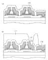
图1是表示本发明的结构的剖面示意图。在图1中,左侧的TFT是被用于驱动电路部的TFT。右侧的TFT是被用于像素部的TFT。任意一个TFT均为使用了poly-Si的底栅型TFT。在像素部的TFT的更右侧形成有端子部。在图1中,为了易于对比而相邻描绘了驱动部TFT、像素部TFT和端子部,但在实际的显示装置中,各元件形成在分离的位置上。Fig. 1 is a schematic sectional view showing the structure of the present invention. In FIG. 1 , the TFTs on the left are TFTs used in the driver circuit section. The TFT on the right is a TFT used in the pixel portion. All TFTs are bottom-gate TFTs using poly-Si. A terminal portion is formed on the further right side of the TFT in the pixel portion. In FIG. 1 , the driver TFT, the pixel TFT, and the terminal are drawn adjacent to each other for easy comparison, but in an actual display device, each element is formed at a separate position.
在图1中,在TFT基板101之上形成有基底膜102。在本实施例中,基底膜102为一层SiN膜,但有时也由SiN和SiO2这两层膜来形成。在基底膜102之上形成有栅电极103,覆盖栅电极103而形成有栅极绝缘膜104。在栅极绝缘膜104之上形成有poly-Si层107。该poly-Si层107成为TFT的沟道部。poly-Si层107的膜厚为50nm左右。In FIG. 1 , a
覆盖poly-Si层107的沟道部而形成有沟道截断环150。利用沟道截断环150来保护TFT的沟道部,并稳定TFT的特性。覆盖沟道截断环150和poly-Si层107而形成有n+Si层109。利用该n+Si层109能够降低截止电流。A
覆盖n+Si层109而形成有源/漏电极(SD电极)113。SD电极113由如下组成构成:基于Mo的屏蔽金属110、Al层111、基于Mo的金属盖层112。如图1所示那样,在本实施例中,n+Si层109和poly-Si层107为面接触,能够减小接触电阻,增加导通电流。利用基于SiN的钝化膜116来保护TFT整体。在钝化膜116之上形成基于有机膜117的平坦化膜,使形成有像素电极119的部分平坦化。A source/drain electrode (SD electrode) 113 is formed covering the n+
在图1中,在驱动电路部用的TFT的右侧示出被用于像素部的TFT。在本实施例中,像素部的TFT也由poly-Si形成。因此在本实施例中,像素部的TFT的结构也与驱动电路部的TFT相同。像素部的TFT的SD电极113与像素电极119导通,对像素部提供数据信号。即,在覆盖像素部TFT的钝化膜116和基于有机膜117的平坦化膜上形成通孔115,通过该通孔115来导通像素电极119和SD电极113。像素电极119利用作为透明导电膜的ITO来形成。In FIG. 1 , TFTs used in the pixel portion are shown on the right side of the TFTs for the driver circuit portion. In this embodiment, the TFT of the pixel portion is also formed of poly-Si. Therefore, also in this embodiment, the structure of the TFT of the pixel part is the same as that of the TFT of the driver circuit part. The
在图1中,在像素部用TFT的更右侧示出端子部。图1中的端子部布线由与SD电极113相同的层形成。即,用与SD电极113相同的材料来与SD电极113同时形成。端子部周边由钝化膜116和作为平坦化膜的有机膜117所保护。在端子部,为了与外部电路连接而在端子部接触孔118处除去钝化膜116和有机膜117。In FIG. 1 , the terminal portion is shown on the further right side of the TFT for a pixel portion. The terminal portion wiring in FIG. 1 is formed of the same layer as the
端子部布线由金属形成,因此容易被外部环境腐蚀。为了防止端子部布线的腐蚀,利用金属氧化物导电膜130覆盖端子部。金属氧化物导电膜130具体而言使用ITO,该端子部的ITO与像素电极119的ITO同时形成。Since the wiring of the terminal portion is formed of metal, it is easily corroded by the external environment. In order to prevent corrosion of wiring at the terminal portion, the terminal portion is covered with a metal oxide conductive film 130 . Specifically, ITO is used for the metal oxide conductive film 130 , and the ITO of the terminal portion is formed simultaneously with the ITO of the
图2~图8表示形成图1所示的TFT和端子部的工序。在图2的(a)中,在TFT基板101之上通过等离子体CVD法而成膜作为基底膜102的SiN。然后,通过溅射而成膜用于形成栅电极103的布线层,并通过光刻步骤来进行加工。考虑到后面的激光退火步骤而以高熔点材料(Mo类)来形成栅电极103。2 to 8 show steps of forming the TFT and the terminal portion shown in FIG. 1 . In (a) of FIG. 2 , SiN is formed as a
在图2的(b)中,通过等离子体CVD法来成膜成为栅极绝缘膜104的SiO2膜,接着通过等离子体CVD法来成膜a-Si膜。该a-Si膜通过激光退火而被转换为poly-Si膜。为了对a-Si膜进行激光退火,进行脱氢处理(450℃以上的退火处理),使a-Si膜中的氢脱离。在图2的(c)中,利用连续振荡的固体激光器产生的激光束106来对a-Si进行poly-Si化。In (b) of FIG. 2 , a SiO2 film to be the
如图3的(a)所示,照射激光后,a-Si层108成为poly-Si层107。在这样形成的poly-Si层107之上,如图3的(b)所示那样,利用SiO类的膜来成膜沟道截断环层150。然后,进行用于加工沟道截断环层150和poly-Si层107的光刻工序。图3的(c)示出通过光刻而在沟道截断环层150之上形成光致抗蚀剂140后的状态。图4的(a)是示出在沟道截断环层150上形成了光致抗蚀剂140的情形的俯视图。As shown in (a) of FIG. 3 , the
在该状态下,用氟酸类的药液进行湿法蚀刻来加工沟道截断环层150。通过进行过蚀刻,发生侧面蚀刻155,使沟道截断环150比抗蚀剂图案窄。图5的(b)示出该状态。沟道截断环层150之下为poly-Si层107,因此poly-Si层107未被蚀刻。在图4的(b)所示的俯视图中,由光致抗蚀剂140覆盖的部分以外呈现poly-Si层107。In this state, the channel
在图5的(a)的状态下,干法蚀刻poly-Si层107。干法蚀刻如图5的(b)的箭头156所示那样,由于没有侧面蚀刻,poly-Si层107被干法蚀刻为与抗蚀剂图案相同的形状。图4的(c)与图5的(b)的俯视图对应,光致抗蚀剂140部分以外被除去poly-Si层107而呈现栅极绝缘膜。In the state of (a) of FIG. 5 , the poly-
然后,除去光致抗蚀剂140。图5的(c)示出除去光致抗蚀剂140后的状态。图6的(a)是与图5的(b)的俯视图对应的图。如图5的(c)和图6的(a)所示那样,在poly-Si层107的周边存在未被沟道截断环层150覆盖的区域。该周边部分成为与在后形成的SD电极113或n+Si层109的接触部,能够减小导通电阻而增大导通电流。Then, the
然后,除去端子部的栅极绝缘膜,形成端子部接触孔118,使端子部露出延伸的栅极布线。然后,通过等离子体CVD来成膜掺杂了P的n+Si层109。接着,通过溅射来成膜SD电极113。SD电极113以与数据信号线相同的层来同时形成。如图7的(b)所示,SD电极113由屏蔽金属层110、Al层111、金属盖层112这三层构成。屏蔽金属层110和金属盖层112层由Mo形成。SD电极113的电导通主要通过Al,Mo被用于防止Al丘、以及在Al与ITO接触的情况下防止Al被氧化而引起的接触不良。Then, the gate insulating film at the terminal portion is removed, and a terminal
接着如图7的(c)所示,通过光刻步骤和蚀刻步骤来加工SD电极113和n+Si层109。首先,通过湿法蚀刻来加工屏蔽金属层110、Al层111以及金属盖层112层这三层。然后,以SD布线层作为掩模,干法蚀刻n+Si层109和poly-Si层107。图6的(b)示出在该干法蚀刻的中途除去n+Si层109后的状态,示出露出poly-Si层107和栅极绝缘膜的状态。Next, as shown in (c) of FIG. 7 , the
接着,将SD电极113和沟道截断环层150作为掩模,进一步进行干法蚀刻,加工poly-Si层107。这样,poly-Si层107如图6的(c)所示,仅存在于沟道截断环层150之下和SD布线之下。图6的(c)的虚线示出poly-Si层107存在的区域。至此,形成底栅型的使用了poly-Si的TFT。Next, using the
接着如图8的(a)所示,通过基于SiN的钝化膜116来覆盖TFT整体。SiN通过等离子体CVD法来成膜。然后如图8的(b)所示,涂敷用于平坦化的感光性有机膜117,通过光刻步骤来进行加工。有机膜117的膜厚为1~2μm左右。将有机膜117作为掩模,蚀刻基于SiN的钝化膜116来形成通孔115。端子部的接触孔118也通过与像素电极119的通孔115相同的工序来同时形成。Next, as shown in (a) of FIG. 8 , the entire TFT is covered with a SiN-based
然后,作为像素电极119,通过溅射来成膜ITO,在光刻中进行加工,形成像素电极119。ITO与像素电极119同时也形成在端子部上。这样,形成图1所示的TFT基板。Then, as the
图9是仅这样形成的TFT部分的详细图。在图9中,比图1所示的稍大地形成poly-Si层107的区域。但是,图1和图9的TFT的结构并没有本质差别,都能够没问题地使用本发明。图9的(a)是TFT的俯视图,图9的(b)是图9的(a)的A-A线剖视图。在图9的(a)中,在由虚线p包围的部分上存在poly-Si层107。如图9的(b)所示,poly-Si层107和n+Si层109在较宽的面状的部分S处接触。poly-Si层107与n+Si层109的接触面积较大,因此该部分的电阻并不对导通电流产生恶劣影响。因此,能够增大导通电流。FIG. 9 is a detailed view of only the TFT portion thus formed. In FIG. 9 , the region of the poly-
(实施例2)(Example 2)
在本实施例中,被使用于像素部的TFT是底栅型的a-Si TFT,被使用于驱动电路部的TFT是底栅型的poly-Si TFT。在此,所谓a-Si TFT是在半导体层使用a-Si的意思,所谓poly-Si TFT是在半导体层使用poly-Si的意思。这是由于:在驱动电路部中,迁移率较大,因此工作较快的poly-Si TFT是有利的,在像素部中,易于减小漏电流的a-Si TFT是有利的。In this embodiment, the TFT used in the pixel portion is a bottom-gate a-Si TFT, and the TFT used in the driver circuit portion is a bottom-gate poly-Si TFT. Here, a-Si TFT means using a-Si in the semiconductor layer, and poly-Si TFT means using poly-Si in the semiconductor layer. This is because poly-Si TFT, which operates faster because of its high mobility, is advantageous in the driver circuit section, and a-Si TFT, which is easy to reduce leakage current, is advantageous in the pixel section.
图10是表示本发明第二实施例的结构的剖面示意图。在图10中,左侧的TFT是被使用于驱动电路部的TFT,TFT由poly-Si形成。驱动电路用TFT需要高速工作,因此使用基于poly-Si的TFT。右侧的TFT是被使用于像素部的TFT,TFT由a-Si形成。这是由于:像素部的TFT相对于高速工作,较小的漏电流是更重要的。Fig. 10 is a schematic sectional view showing the structure of a second embodiment of the present invention. In FIG. 10 , the TFT on the left is a TFT used in the driver circuit section, and the TFT is formed of poly-Si. TFTs for driving circuits require high-speed operation, so poly-Si-based TFTs are used. The TFT on the right is a TFT used in the pixel portion, and the TFT is made of a-Si. This is because a small leakage current is more important than a high-speed operation of the TFT in the pixel portion.
像素部的TFT的更右侧形成有端子部。在图1中,为了易于对比而相邻描绘了驱动部TFT、像素部TFT、端子部,但在实际的显示装置中,各像素形成在分离的位置。在图10中,除了像素部的TFT由a-Si形成之外,其余与实施例1的图1相同,因此省略其他说明。A terminal portion is formed on the far right side of the TFT of the pixel portion. In FIG. 1 , the driver TFT, the pixel TFT, and the terminal are drawn adjacent to each other for easy comparison, but in an actual display device, each pixel is formed at a separate position. In FIG. 10 , except that the TFT of the pixel portion is formed of a-Si, the rest is the same as that in FIG. 1 of the first embodiment, so other explanations are omitted.
图11~图14示出形成图10所示的TFT和端子部的工序。在图11的(a)中,在TFT基板101之上通过等离子体CVD法来成膜作为基底膜102的SiN。然后,通过溅射来成膜用于形成栅电极103的布线层,通过光刻步骤来对其进行加工。考虑到之后的激光退火步骤,栅电极103用高熔点材料(Mo类)来形成。11 to 14 show steps of forming the TFT and terminal portion shown in FIG. 10 . In (a) of FIG. 11 , SiN is formed as the
在图11的(b)中,通过等离子体CVD法来成膜成为栅极绝缘膜104的SiO2膜,接着通过等离子体CVD法来成膜a-Si膜。在驱动电路部中,a-Si膜通过激光退火而被转换为poly-Si膜。激光使用受激准分子激光,但能够通过受激准分子激光将a-Si转换为poly-Si的膜厚存在限度,为70nm以下。另外,本实施例中的典型的a-Si膜的厚度为50nm。在本实施例中,poly-Si TFT的部分、a-Si TFT的部分都在同一工序中形成,因此a-Si层108、poly-Si层107都为50nm。In (b) of FIG. 11 , a SiO2 film to be the
在形成a-Si膜之后,如图11的(c)所示,仅对与驱动电路部对应的部分的a-Si膜照射激光1061,加热至450℃左右,进行脱氢处理。这是为了防止在之后使驱动电路部分的a-Si膜结晶化时的退火中氢的爆沸。这样如图12的(a)所示,存在堆积a-Si层后的状态的a-Si层108和脱氢a-Si层区域1081。After forming the a-Si film, as shown in (c) of FIG. 11 , only the portion of the a-Si film corresponding to the driver circuit portion is irradiated with
然后,如图12的(b)所示,对进行了脱氢处理的与驱动电路部对应的区域的脱氢a-Si层区域1081照射激光,将a-Si膜转换为poly-Si膜。这样,如图12的(c)所示,在一块基板之上形成poly-Si层107和a-Si层108的区域的半导体膜。在图12的(c)中,在形成poly-Si膜的区域的周边残留进行了脱氢处理的a-Si膜1081。通过激光处理将a-Si膜转换为poly-Si膜时,使进行脱氢处理的区域大于poly-Si区域来确保工序的富余,使得不发生氢的爆沸。Then, as shown in FIG. 12( b ), the dehydrogenated
然后如图13的(a)所示,通过SiO类的膜来在基板整个面上成膜沟道截断环层150。接着,进行用于加工沟道截断环层150和poly-Si层107的光刻工序。图13的(b)示出通过光刻来在沟道截断环层150之上形成光致抗蚀剂140后的状态。Next, as shown in (a) of FIG. 13 , a channel
在该状态下,用氟酸类药液进行湿法蚀刻,加工沟道截断环层150。通过过腐蚀,发生侧面蚀刻155,使沟道截断环150比抗蚀剂图案窄。图13的(c)示出该状态。该加工在poly-Si区域、a-Si区域中共同进行。沟道截断环层150之下是poly-Si层107或a-Si层108,因此未被蚀刻。In this state, the channel
在图13的(c)的状态下,干法蚀刻poly-Si层107和a-Si层108。干法蚀刻如图14的(a)的箭头156所示的那样,由于没有侧面蚀刻,poly-Si层107和a-Si层108被干法蚀刻为与抗蚀剂图案相同的形状。In the state of (c) of FIG. 13 , the poly-
然后,除去光致抗蚀剂140。图14的(b)示出除去光致抗蚀剂140后的状态。如图14的(b)所示,在poly-Si层107和a-Si层108的周边存在未被沟道截断环层150覆盖的区域。该周边部分成为与在后形成的SD电极113的接触部,能够减少导通电阻而增大导通电流。Then, the
通常在s-Si TFT中,不是采用沟道截断环150而是采用沟道蚀刻结构。这是因为:在通常的a-Si TFT中,a-Si层108的膜厚较大,因此具有进行沟道蚀刻的余地。但是,本实施例的a-Si TFT的a-Si膜无法厚到50nm左右,因此使用沟道截断环150结构。Usually in s-Si TFT, instead of using the
省略图示,但除去端子部的栅极绝缘膜,形成端子部接触孔118,使端子部露出延伸的栅极布线。然后,通过等离子体CVD成膜掺杂了P的n+Si层109。接着,通过溅射成膜SD电极113。SD电极113由屏蔽金属层110、Al层111、金属盖层112这三层构成。SD电极113的结构如实施例1中说明的那样。Although not shown, the gate insulating film at the terminal portion is removed, and a terminal
接着如图14的(c)所示,通过光刻步骤和蚀刻步骤来加工SD电极113和n+Si层109。首先,通过湿法蚀刻来加工屏蔽金属层110、Al层111以及金属盖层112层这三层。然后,将SD布线层作为掩模,干法蚀刻n+Si层109和poly-Si层107或a-Si层108和poly-Si层107。Next, as shown in (c) of FIG. 14 , the
于是,poly-Si层107或a-Si层108仅存在于沟道截断环层150之下和SD布线之下。这样,形成底栅型的使用了poly-Si的TFT和使用了a-Si的TFT。Then, the poly-
接着,通过基于SiN的钝化膜116来覆盖TFT整体。SiN通过等离子体CVD法来成膜。然后,涂敷用于平坦化的感光性有机膜117,通过光刻步骤对其进行加工。有机膜117的膜厚为1~2μm左右。将有机膜117作为掩模,蚀刻基于SiN的钝化膜116来形成通孔115。端子部的接触孔118也通过与像素电极119的通孔115相同的工序来同时形成。Next, the entire TFT is covered with a SiN-based
然后,通过溅射成膜ITO来作为像素电极119,在光刻中进行加工,形成像素电极119。ITO与像素电极119同时也形成在端子部。这样,形成图10所示的TFT基板。Then, ITO was formed into a film by sputtering as the
这样,根据本实施例,能够在相同的工序中同时形成poly-Si型TFT和a-Si型TFT。另外,能够在同一基板上形成具有导通电流较大的poly-Si型TFT、截止电流较小的a-Si型TFT这样的各种特征的TFT。Thus, according to this embodiment, poly-Si type TFTs and a-Si type TFTs can be simultaneously formed in the same process. In addition, TFTs having various characteristics such as a poly-Si type TFT having a large on-current and an a-Si type TFT having a small off-current can be formed on the same substrate.
Claims (7)
Applications Claiming Priority (3)
| Application Number | Priority Date | Filing Date | Title |
|---|---|---|---|
| JP2008056718 | 2008-03-06 | ||
| JP2008056718AJP2009211009A (en) | 2008-03-06 | 2008-03-06 | Liquid crystal display device |
| JP2008-056718 | 2008-03-06 |
Publications (2)
| Publication Number | Publication Date |
|---|---|
| CN101526709Atrue CN101526709A (en) | 2009-09-09 |
| CN101526709B CN101526709B (en) | 2011-04-20 |
Family
ID=41053225
Family Applications (1)
| Application Number | Title | Priority Date | Filing Date |
|---|---|---|---|
| CN2009101266410AActiveCN101526709B (en) | 2008-03-06 | 2009-03-05 | Liquid crystal display divice |
Country Status (3)
| Country | Link |
|---|---|
| US (1) | US20090225251A1 (en) |
| JP (1) | JP2009211009A (en) |
| CN (1) | CN101526709B (en) |
Cited By (2)
| Publication number | Priority date | Publication date | Assignee | Title |
|---|---|---|---|---|
| CN101997005A (en)* | 2009-08-07 | 2011-03-30 | 株式会社半导体能源研究所 | Semiconductor device and method for manufacturing the same |
| CN103222061A (en)* | 2010-11-12 | 2013-07-24 | 株式会社神户制钢所 | Wiring structure |
Families Citing this family (17)
| Publication number | Priority date | Publication date | Assignee | Title |
|---|---|---|---|---|
| JP5111167B2 (en)* | 2008-03-06 | 2012-12-26 | 株式会社ジャパンディスプレイイースト | Liquid crystal display |
| JP5663231B2 (en)* | 2009-08-07 | 2015-02-04 | 株式会社半導体エネルギー研究所 | Light emitting device |
| TWI604594B (en)* | 2009-08-07 | 2017-11-01 | 半導體能源研究所股份有限公司 | Semiconductor device and telephone, watch, and display device including the same |
| US8115883B2 (en) | 2009-08-27 | 2012-02-14 | Semiconductor Energy Laboratory Co., Ltd. | Display device and method for manufacturing the same |
| US20110050168A1 (en)* | 2009-08-27 | 2011-03-03 | Electronics And Telecommunications Research Institute | Charge control method for vehicle and device thereof |
| WO2011027702A1 (en) | 2009-09-04 | 2011-03-10 | Semiconductor Energy Laboratory Co., Ltd. | Light-emitting device and method for manufacturing the same |
| KR101602635B1 (en)* | 2009-11-30 | 2016-03-22 | 삼성디스플레이 주식회사 | Display devise, thin film transistor substrate and method of fabricating the same |
| KR101797253B1 (en)* | 2009-12-04 | 2017-11-13 | 가부시키가이샤 한도오따이 에네루기 켄큐쇼 | Semiconductor device and manufacturing method thereof |
| KR20110093113A (en)* | 2010-02-11 | 2011-08-18 | 삼성전자주식회사 | Thin film transistor substrate and manufacturing method thereof |
| JP5662689B2 (en)* | 2010-02-17 | 2015-02-04 | 株式会社ジャパンディスプレイ | Display device and manufacturing method thereof |
| US20130208207A1 (en)* | 2010-06-25 | 2013-08-15 | Sharp Kabushiki Kaisha | Display device substrate, method for producing the same, and display device |
| JP5917127B2 (en)* | 2011-12-19 | 2016-05-11 | 株式会社ジャパンディスプレイ | Liquid crystal display |
| KR102281300B1 (en) | 2013-09-11 | 2021-07-26 | 삼성디스플레이 주식회사 | Thin film transistor, method of manufacturing the same, and display device including the same |
| CN104362157B (en)* | 2014-12-02 | 2017-05-03 | 京东方科技集团股份有限公司 | Array substrate and production method thereof and display device |
| CN104867812A (en)* | 2015-03-27 | 2015-08-26 | 京东方科技集团股份有限公司 | Preparation methods of polysilicon film and semiconductor device, and display substrate and apparatus |
| KR102563157B1 (en)* | 2015-08-26 | 2023-08-04 | 엘지디스플레이 주식회사 | Thin film transistor and display device |
| US11695039B2 (en)* | 2021-07-30 | 2023-07-04 | Taiwan Semiconductor Manufacturing Company, Ltd. | Semiconductor device including an active component and a barrier pattern surrounding the active component and method of forming the same |
Family Cites Families (2)
| Publication number | Priority date | Publication date | Assignee | Title |
|---|---|---|---|---|
| KR100584715B1 (en)* | 2004-04-06 | 2006-05-29 | 엘지.필립스 엘시디 주식회사 | Manufacturing method of array substrate for liquid crystal display device with integrated drive circuit |
| US20070002199A1 (en)* | 2005-06-30 | 2007-01-04 | Semiconductor Energy Laboratory Co., Ltd. | Liquid crystal display device and method for manufacturing the same |
- 2008
- 2008-03-06JPJP2008056718Apatent/JP2009211009A/ennot_activeWithdrawn
- 2009
- 2009-03-05CNCN2009101266410Apatent/CN101526709B/enactiveActive
- 2009-03-05USUS12/398,274patent/US20090225251A1/ennot_activeAbandoned
Cited By (4)
| Publication number | Priority date | Publication date | Assignee | Title |
|---|---|---|---|---|
| CN101997005A (en)* | 2009-08-07 | 2011-03-30 | 株式会社半导体能源研究所 | Semiconductor device and method for manufacturing the same |
| CN101997005B (en)* | 2009-08-07 | 2015-11-25 | 株式会社半导体能源研究所 | Semiconductor device and manufacture method thereof |
| CN103222061A (en)* | 2010-11-12 | 2013-07-24 | 株式会社神户制钢所 | Wiring structure |
| CN103222061B (en)* | 2010-11-12 | 2016-11-09 | 株式会社神户制钢所 | Wiring structure |
Also Published As
| Publication number | Publication date |
|---|---|
| US20090225251A1 (en) | 2009-09-10 |
| CN101526709B (en) | 2011-04-20 |
| JP2009211009A (en) | 2009-09-17 |
Similar Documents
| Publication | Publication Date | Title |
|---|---|---|
| CN101526709A (en) | Liquid crystal display divice | |
| US8440483B2 (en) | Method of fabricating array substrate | |
| JP5226259B2 (en) | Liquid crystal display | |
| KR101272892B1 (en) | Array substrate | |
| JP4850057B2 (en) | Liquid crystal display device and manufacturing method thereof | |
| US20130037807A1 (en) | Semiconductor device and method for manufacturing the same | |
| US20120199891A1 (en) | Semiconductor device and method for manufacturing same | |
| US8415666B2 (en) | Thin film transistor substrate having thin film transistors with improved etching characteristics, method of manufacturing the same, and display apparatus having the same | |
| KR100831881B1 (en) | Thin-film semiconductor device | |
| KR101246789B1 (en) | Array substrate and method of fabricating the same | |
| CN110729313A (en) | Display panel, display panel preparation method and display device | |
| US9842915B2 (en) | Array substrate for liquid crystal display device and method of manufacturing the same | |
| CN210723028U (en) | Display panel and display device | |
| US7994505B2 (en) | Liquid crystal display device | |
| US20170184893A1 (en) | Semiconductor apparatus, method of manufacturing same, and liquid crystal display apparatus | |
| CN114649259A (en) | Method for manufacturing display device | |
| KR20120043404A (en) | Display apparatus and method of manufacturing the same | |
| US10804406B2 (en) | Thin-film transistor substrate, liquid crystal display device including the same, and method for producing thin-film transistor substrate | |
| JP2010129881A (en) | Thin-film transistor and active matrix substrate | |
| WO2017028493A1 (en) | Thin film transistor and manufacturing method therefor, and display device | |
| CN115084277A (en) | Metal oxide thin film transistor, method for making the same, and array substrate | |
| WO2012169388A1 (en) | Tft substrate and method for manufacturing same | |
| KR102536563B1 (en) | Display apparatus | |
| US8735890B2 (en) | Display substrate and method of manufacturing the display substrate | |
| KR101518851B1 (en) | Method of fabricating array substrate |
Legal Events
| Date | Code | Title | Description |
|---|---|---|---|
| C06 | Publication | ||
| PB01 | Publication | ||
| C10 | Entry into substantive examination | ||
| SE01 | Entry into force of request for substantive examination | ||
| C14 | Grant of patent or utility model | ||
| GR01 | Patent grant | ||
| ASS | Succession or assignment of patent right | Owner name:IPS ALPHA SUPPORT CO., LTD. Owner name:PANASONIC LCD CO., LTD. Free format text:FORMER OWNER: IPS ALPHA SUPPORT CO., LTD. | |
| C41 | Transfer of patent application or patent right or utility model | ||
| TR01 | Transfer of patent right | Effective date of registration:20110928 Address after:Chiba County, Japan Co-patentee after:Panasonic Liquid Crystal Display Co.,Ltd. Patentee after:Hitachi Displays, Ltd. Address before:Chiba County, Japan Co-patentee before:IPS pioneer support society Patentee before:Hitachi Displays, Ltd. Effective date of registration:20110928 Address after:Chiba County, Japan Co-patentee after:IPS Pioneer Support Society Patentee after:Hitachi Displays, Ltd. Address before:Chiba County, Japan Patentee before:Hitachi Displays, Ltd. | |
| C56 | Change in the name or address of the patentee | Owner name:APAN DISPLAY EAST, INC. Free format text:FORMER NAME: HITACHI DISPLAY CO., LTD. Owner name:JAPAN DISPLAY, INC. Free format text:FORMER NAME: APAN DISPLAY EAST, INC. | |
| CP01 | Change in the name or title of a patent holder | Address after:Chiba County, Japan Patentee after:Japan Display East Inc. Patentee after:Panasonic Liquid Crystal Display Co.,Ltd. Address before:Chiba County, Japan Patentee before:Hitachi Displays, Ltd. Patentee before:Panasonic Liquid Crystal Display Co.,Ltd. | |
| CP03 | Change of name, title or address | Address after:Tokyo port xixinqiao Japan three chome 7 No. 1 Patentee after:JAPAN DISPLAY Inc. Patentee after:Panasonic Liquid Crystal Display Co.,Ltd. Address before:Chiba County, Japan Patentee before:Japan Display East Inc. Patentee before:Panasonic Liquid Crystal Display Co.,Ltd. | |
| EE01 | Entry into force of recordation of patent licensing contract | Application publication date:20090909 Assignee:BOE TECHNOLOGY GROUP Co.,Ltd. Assignor:JAPAN DISPLAY Inc.|Panasonic Liquid Crystal Display Co.,Ltd. Contract record no.:2013990000688 Denomination of invention:Liquid crystal display device Granted publication date:20110420 License type:Common License Record date:20131016 | |
| LICC | Enforcement, change and cancellation of record of contracts on the licence for exploitation of a patent or utility model | ||
| TR01 | Transfer of patent right | ||
| TR01 | Transfer of patent right | Effective date of registration:20231206 Address after:Tokyo, Japan Patentee after:JAPAN DISPLAY Inc. Patentee after:PANASONIC INTELLECTUAL PROPERTY CORPORATION OF AMERICA Address before:Tokyo port xixinqiao Japan three chome 7 No. 1 Patentee before:JAPAN DISPLAY Inc. Patentee before:Panasonic Liquid Crystal Display Co.,Ltd. | |
| TR01 | Transfer of patent right | Effective date of registration:20250729 Address after:Tokyo, Japan Patentee after:Magno Zichen Co.,Ltd. Country or region after:Japan Patentee after:PANASONIC INTELLECTUAL PROPERTY CORPORATION OF AMERICA Country or region after:U.S.A. Address before:Tokyo, Japan Patentee before:JAPAN DISPLAY Inc. Country or region before:Japan Patentee before:PANASONIC INTELLECTUAL PROPERTY CORPORATION OF AMERICA Country or region before:U.S.A. | |
| TR01 | Transfer of patent right |