CN101515102A - Flat display device and method for manufacturing the same - Google Patents
Flat display device and method for manufacturing the sameDownload PDFInfo
- Publication number
- CN101515102A CN101515102ACNA2008101764869ACN200810176486ACN101515102ACN 101515102 ACN101515102 ACN 101515102ACN A2008101764869 ACNA2008101764869 ACN A2008101764869ACN 200810176486 ACN200810176486 ACN 200810176486ACN 101515102 ACN101515102 ACN 101515102A
- Authority
- CN
- China
- Prior art keywords
- electrode
- pixel
- panel display
- display device
- layer
- Prior art date
- Legal status (The legal status is an assumption and is not a legal conclusion. Google has not performed a legal analysis and makes no representation as to the accuracy of the status listed.)
- Granted
Links
Images


Classifications
- G—PHYSICS
- G02—OPTICS
- G02F—OPTICAL DEVICES OR ARRANGEMENTS FOR THE CONTROL OF LIGHT BY MODIFICATION OF THE OPTICAL PROPERTIES OF THE MEDIA OF THE ELEMENTS INVOLVED THEREIN; NON-LINEAR OPTICS; FREQUENCY-CHANGING OF LIGHT; OPTICAL LOGIC ELEMENTS; OPTICAL ANALOGUE/DIGITAL CONVERTERS
- G02F1/00—Devices or arrangements for the control of the intensity, colour, phase, polarisation or direction of light arriving from an independent light source, e.g. switching, gating or modulating; Non-linear optics
- G02F1/01—Devices or arrangements for the control of the intensity, colour, phase, polarisation or direction of light arriving from an independent light source, e.g. switching, gating or modulating; Non-linear optics for the control of the intensity, phase, polarisation or colour
- G02F1/13—Devices or arrangements for the control of the intensity, colour, phase, polarisation or direction of light arriving from an independent light source, e.g. switching, gating or modulating; Non-linear optics for the control of the intensity, phase, polarisation or colour based on liquid crystals, e.g. single liquid crystal display cells
- G02F1/133—Constructional arrangements; Operation of liquid crystal cells; Circuit arrangements
- G02F1/136—Liquid crystal cells structurally associated with a semi-conducting layer or substrate, e.g. cells forming part of an integrated circuit
- G02F1/1362—Active matrix addressed cells
- G02F1/136213—Storage capacitors associated with the pixel electrode
- G—PHYSICS
- G02—OPTICS
- G02F—OPTICAL DEVICES OR ARRANGEMENTS FOR THE CONTROL OF LIGHT BY MODIFICATION OF THE OPTICAL PROPERTIES OF THE MEDIA OF THE ELEMENTS INVOLVED THEREIN; NON-LINEAR OPTICS; FREQUENCY-CHANGING OF LIGHT; OPTICAL LOGIC ELEMENTS; OPTICAL ANALOGUE/DIGITAL CONVERTERS
- G02F1/00—Devices or arrangements for the control of the intensity, colour, phase, polarisation or direction of light arriving from an independent light source, e.g. switching, gating or modulating; Non-linear optics
- G02F1/01—Devices or arrangements for the control of the intensity, colour, phase, polarisation or direction of light arriving from an independent light source, e.g. switching, gating or modulating; Non-linear optics for the control of the intensity, phase, polarisation or colour
- G02F1/13—Devices or arrangements for the control of the intensity, colour, phase, polarisation or direction of light arriving from an independent light source, e.g. switching, gating or modulating; Non-linear optics for the control of the intensity, phase, polarisation or colour based on liquid crystals, e.g. single liquid crystal display cells
- G02F1/133—Constructional arrangements; Operation of liquid crystal cells; Circuit arrangements
- G02F1/1333—Constructional arrangements; Manufacturing methods
- G02F1/1343—Electrodes
- B—PERFORMING OPERATIONS; TRANSPORTING
- B82—NANOTECHNOLOGY
- B82Y—SPECIFIC USES OR APPLICATIONS OF NANOSTRUCTURES; MEASUREMENT OR ANALYSIS OF NANOSTRUCTURES; MANUFACTURE OR TREATMENT OF NANOSTRUCTURES
- B82Y20/00—Nanooptics, e.g. quantum optics or photonic crystals
- G—PHYSICS
- G02—OPTICS
- G02F—OPTICAL DEVICES OR ARRANGEMENTS FOR THE CONTROL OF LIGHT BY MODIFICATION OF THE OPTICAL PROPERTIES OF THE MEDIA OF THE ELEMENTS INVOLVED THEREIN; NON-LINEAR OPTICS; FREQUENCY-CHANGING OF LIGHT; OPTICAL LOGIC ELEMENTS; OPTICAL ANALOGUE/DIGITAL CONVERTERS
- G02F1/00—Devices or arrangements for the control of the intensity, colour, phase, polarisation or direction of light arriving from an independent light source, e.g. switching, gating or modulating; Non-linear optics
- G02F1/01—Devices or arrangements for the control of the intensity, colour, phase, polarisation or direction of light arriving from an independent light source, e.g. switching, gating or modulating; Non-linear optics for the control of the intensity, phase, polarisation or colour
- G02F1/13—Devices or arrangements for the control of the intensity, colour, phase, polarisation or direction of light arriving from an independent light source, e.g. switching, gating or modulating; Non-linear optics for the control of the intensity, phase, polarisation or colour based on liquid crystals, e.g. single liquid crystal display cells
- G02F1/133—Constructional arrangements; Operation of liquid crystal cells; Circuit arrangements
- G02F1/136—Liquid crystal cells structurally associated with a semi-conducting layer or substrate, e.g. cells forming part of an integrated circuit
- G—PHYSICS
- G02—OPTICS
- G02F—OPTICAL DEVICES OR ARRANGEMENTS FOR THE CONTROL OF LIGHT BY MODIFICATION OF THE OPTICAL PROPERTIES OF THE MEDIA OF THE ELEMENTS INVOLVED THEREIN; NON-LINEAR OPTICS; FREQUENCY-CHANGING OF LIGHT; OPTICAL LOGIC ELEMENTS; OPTICAL ANALOGUE/DIGITAL CONVERTERS
- G02F1/00—Devices or arrangements for the control of the intensity, colour, phase, polarisation or direction of light arriving from an independent light source, e.g. switching, gating or modulating; Non-linear optics
- G02F1/01—Devices or arrangements for the control of the intensity, colour, phase, polarisation or direction of light arriving from an independent light source, e.g. switching, gating or modulating; Non-linear optics for the control of the intensity, phase, polarisation or colour
- G02F1/13—Devices or arrangements for the control of the intensity, colour, phase, polarisation or direction of light arriving from an independent light source, e.g. switching, gating or modulating; Non-linear optics for the control of the intensity, phase, polarisation or colour based on liquid crystals, e.g. single liquid crystal display cells
- G02F1/1306—Details
- G02F1/1309—Repairing; Testing
- G—PHYSICS
- G02—OPTICS
- G02F—OPTICAL DEVICES OR ARRANGEMENTS FOR THE CONTROL OF LIGHT BY MODIFICATION OF THE OPTICAL PROPERTIES OF THE MEDIA OF THE ELEMENTS INVOLVED THEREIN; NON-LINEAR OPTICS; FREQUENCY-CHANGING OF LIGHT; OPTICAL LOGIC ELEMENTS; OPTICAL ANALOGUE/DIGITAL CONVERTERS
- G02F1/00—Devices or arrangements for the control of the intensity, colour, phase, polarisation or direction of light arriving from an independent light source, e.g. switching, gating or modulating; Non-linear optics
- G02F1/01—Devices or arrangements for the control of the intensity, colour, phase, polarisation or direction of light arriving from an independent light source, e.g. switching, gating or modulating; Non-linear optics for the control of the intensity, phase, polarisation or colour
- G02F1/13—Devices or arrangements for the control of the intensity, colour, phase, polarisation or direction of light arriving from an independent light source, e.g. switching, gating or modulating; Non-linear optics for the control of the intensity, phase, polarisation or colour based on liquid crystals, e.g. single liquid crystal display cells
- G02F1/133—Constructional arrangements; Operation of liquid crystal cells; Circuit arrangements
- G02F1/1333—Constructional arrangements; Manufacturing methods
- G02F1/133388—Constructional arrangements; Manufacturing methods with constructional differences between the display region and the peripheral region
- G—PHYSICS
- G02—OPTICS
- G02F—OPTICAL DEVICES OR ARRANGEMENTS FOR THE CONTROL OF LIGHT BY MODIFICATION OF THE OPTICAL PROPERTIES OF THE MEDIA OF THE ELEMENTS INVOLVED THEREIN; NON-LINEAR OPTICS; FREQUENCY-CHANGING OF LIGHT; OPTICAL LOGIC ELEMENTS; OPTICAL ANALOGUE/DIGITAL CONVERTERS
- G02F1/00—Devices or arrangements for the control of the intensity, colour, phase, polarisation or direction of light arriving from an independent light source, e.g. switching, gating or modulating; Non-linear optics
- G02F1/01—Devices or arrangements for the control of the intensity, colour, phase, polarisation or direction of light arriving from an independent light source, e.g. switching, gating or modulating; Non-linear optics for the control of the intensity, phase, polarisation or colour
- G02F1/13—Devices or arrangements for the control of the intensity, colour, phase, polarisation or direction of light arriving from an independent light source, e.g. switching, gating or modulating; Non-linear optics for the control of the intensity, phase, polarisation or colour based on liquid crystals, e.g. single liquid crystal display cells
- G02F1/133—Constructional arrangements; Operation of liquid crystal cells; Circuit arrangements
- G02F1/1333—Constructional arrangements; Manufacturing methods
- G02F1/1335—Structural association of cells with optical devices, e.g. polarisers or reflectors
- G02F1/133553—Reflecting elements
- G—PHYSICS
- G02—OPTICS
- G02F—OPTICAL DEVICES OR ARRANGEMENTS FOR THE CONTROL OF LIGHT BY MODIFICATION OF THE OPTICAL PROPERTIES OF THE MEDIA OF THE ELEMENTS INVOLVED THEREIN; NON-LINEAR OPTICS; FREQUENCY-CHANGING OF LIGHT; OPTICAL LOGIC ELEMENTS; OPTICAL ANALOGUE/DIGITAL CONVERTERS
- G02F1/00—Devices or arrangements for the control of the intensity, colour, phase, polarisation or direction of light arriving from an independent light source, e.g. switching, gating or modulating; Non-linear optics
- G02F1/01—Devices or arrangements for the control of the intensity, colour, phase, polarisation or direction of light arriving from an independent light source, e.g. switching, gating or modulating; Non-linear optics for the control of the intensity, phase, polarisation or colour
- G02F1/13—Devices or arrangements for the control of the intensity, colour, phase, polarisation or direction of light arriving from an independent light source, e.g. switching, gating or modulating; Non-linear optics for the control of the intensity, phase, polarisation or colour based on liquid crystals, e.g. single liquid crystal display cells
- G02F1/133—Constructional arrangements; Operation of liquid crystal cells; Circuit arrangements
- G02F1/136—Liquid crystal cells structurally associated with a semi-conducting layer or substrate, e.g. cells forming part of an integrated circuit
- G02F1/13606—Liquid crystal cells structurally associated with a semi-conducting layer or substrate, e.g. cells forming part of an integrated circuit having means for reducing parasitic capacitance
- G—PHYSICS
- G02—OPTICS
- G02F—OPTICAL DEVICES OR ARRANGEMENTS FOR THE CONTROL OF LIGHT BY MODIFICATION OF THE OPTICAL PROPERTIES OF THE MEDIA OF THE ELEMENTS INVOLVED THEREIN; NON-LINEAR OPTICS; FREQUENCY-CHANGING OF LIGHT; OPTICAL LOGIC ELEMENTS; OPTICAL ANALOGUE/DIGITAL CONVERTERS
- G02F1/00—Devices or arrangements for the control of the intensity, colour, phase, polarisation or direction of light arriving from an independent light source, e.g. switching, gating or modulating; Non-linear optics
- G02F1/01—Devices or arrangements for the control of the intensity, colour, phase, polarisation or direction of light arriving from an independent light source, e.g. switching, gating or modulating; Non-linear optics for the control of the intensity, phase, polarisation or colour
- G02F1/13—Devices or arrangements for the control of the intensity, colour, phase, polarisation or direction of light arriving from an independent light source, e.g. switching, gating or modulating; Non-linear optics for the control of the intensity, phase, polarisation or colour based on liquid crystals, e.g. single liquid crystal display cells
- G02F1/133—Constructional arrangements; Operation of liquid crystal cells; Circuit arrangements
- G02F1/136—Liquid crystal cells structurally associated with a semi-conducting layer or substrate, e.g. cells forming part of an integrated circuit
- G02F1/1362—Active matrix addressed cells
- G02F1/136204—Arrangements to prevent high voltage or static electricity failures
- G—PHYSICS
- G02—OPTICS
- G02F—OPTICAL DEVICES OR ARRANGEMENTS FOR THE CONTROL OF LIGHT BY MODIFICATION OF THE OPTICAL PROPERTIES OF THE MEDIA OF THE ELEMENTS INVOLVED THEREIN; NON-LINEAR OPTICS; FREQUENCY-CHANGING OF LIGHT; OPTICAL LOGIC ELEMENTS; OPTICAL ANALOGUE/DIGITAL CONVERTERS
- G02F1/00—Devices or arrangements for the control of the intensity, colour, phase, polarisation or direction of light arriving from an independent light source, e.g. switching, gating or modulating; Non-linear optics
- G02F1/01—Devices or arrangements for the control of the intensity, colour, phase, polarisation or direction of light arriving from an independent light source, e.g. switching, gating or modulating; Non-linear optics for the control of the intensity, phase, polarisation or colour
- G02F1/13—Devices or arrangements for the control of the intensity, colour, phase, polarisation or direction of light arriving from an independent light source, e.g. switching, gating or modulating; Non-linear optics for the control of the intensity, phase, polarisation or colour based on liquid crystals, e.g. single liquid crystal display cells
- G02F1/133—Constructional arrangements; Operation of liquid crystal cells; Circuit arrangements
- G02F1/136—Liquid crystal cells structurally associated with a semi-conducting layer or substrate, e.g. cells forming part of an integrated circuit
- G02F1/1362—Active matrix addressed cells
- G02F1/136231—Active matrix addressed cells for reducing the number of lithographic steps
- G02F1/136236—Active matrix addressed cells for reducing the number of lithographic steps using a grey or half tone lithographic process
- G—PHYSICS
- G02—OPTICS
- G02F—OPTICAL DEVICES OR ARRANGEMENTS FOR THE CONTROL OF LIGHT BY MODIFICATION OF THE OPTICAL PROPERTIES OF THE MEDIA OF THE ELEMENTS INVOLVED THEREIN; NON-LINEAR OPTICS; FREQUENCY-CHANGING OF LIGHT; OPTICAL LOGIC ELEMENTS; OPTICAL ANALOGUE/DIGITAL CONVERTERS
- G02F1/00—Devices or arrangements for the control of the intensity, colour, phase, polarisation or direction of light arriving from an independent light source, e.g. switching, gating or modulating; Non-linear optics
- G02F1/01—Devices or arrangements for the control of the intensity, colour, phase, polarisation or direction of light arriving from an independent light source, e.g. switching, gating or modulating; Non-linear optics for the control of the intensity, phase, polarisation or colour
- G02F1/165—Devices or arrangements for the control of the intensity, colour, phase, polarisation or direction of light arriving from an independent light source, e.g. switching, gating or modulating; Non-linear optics for the control of the intensity, phase, polarisation or colour based on translational movement of particles in a fluid under the influence of an applied field
- G02F1/1675—Constructional details
- G02F1/1679—Gaskets; Spacers; Sealing of cells; Filling or closing of cells
- G02F1/1681—Gaskets; Spacers; Sealing of cells; Filling or closing of cells having two or more microcells partitioned by walls, e.g. of microcup type
- G—PHYSICS
- G02—OPTICS
- G02F—OPTICAL DEVICES OR ARRANGEMENTS FOR THE CONTROL OF LIGHT BY MODIFICATION OF THE OPTICAL PROPERTIES OF THE MEDIA OF THE ELEMENTS INVOLVED THEREIN; NON-LINEAR OPTICS; FREQUENCY-CHANGING OF LIGHT; OPTICAL LOGIC ELEMENTS; OPTICAL ANALOGUE/DIGITAL CONVERTERS
- G02F2201/00—Constructional arrangements not provided for in groups G02F1/00 - G02F7/00
- G02F2201/50—Protective arrangements
- G—PHYSICS
- G02—OPTICS
- G02F—OPTICAL DEVICES OR ARRANGEMENTS FOR THE CONTROL OF LIGHT BY MODIFICATION OF THE OPTICAL PROPERTIES OF THE MEDIA OF THE ELEMENTS INVOLVED THEREIN; NON-LINEAR OPTICS; FREQUENCY-CHANGING OF LIGHT; OPTICAL LOGIC ELEMENTS; OPTICAL ANALOGUE/DIGITAL CONVERTERS
- G02F2202/00—Materials and properties
- G02F2202/36—Micro- or nanomaterials
- H—ELECTRICITY
- H10—SEMICONDUCTOR DEVICES; ELECTRIC SOLID-STATE DEVICES NOT OTHERWISE PROVIDED FOR
- H10D—INORGANIC ELECTRIC SEMICONDUCTOR DEVICES
- H10D30/00—Field-effect transistors [FET]
- H10D30/60—Insulated-gate field-effect transistors [IGFET]
- H10D30/67—Thin-film transistors [TFT]
- H10D30/6729—Thin-film transistors [TFT] characterised by the electrodes
- H10D30/673—Thin-film transistors [TFT] characterised by the electrodes characterised by the shapes, relative sizes or dispositions of the gate electrodes
Landscapes
- Physics & Mathematics (AREA)
- Engineering & Computer Science (AREA)
- Nonlinear Science (AREA)
- Chemical & Material Sciences (AREA)
- Optics & Photonics (AREA)
- Crystallography & Structural Chemistry (AREA)
- General Physics & Mathematics (AREA)
- Mathematical Physics (AREA)
- Nanotechnology (AREA)
- Microelectronics & Electronic Packaging (AREA)
- Power Engineering (AREA)
- Life Sciences & Earth Sciences (AREA)
- Biophysics (AREA)
- Liquid Crystal (AREA)
- Devices For Indicating Variable Information By Combining Individual Elements (AREA)
Abstract
Translated fromChineseDescription
Translated fromChinese本发明要求享有2008年2月19日提交的韩国专利申请No.2008-0014899的权益,在此引入其全部内容作为参考。This application claims the benefit of Korean Patent Application No. 2008-0014899 filed on February 19, 2008, the entire contents of which are hereby incorporated by reference.
技术领域technical field
本发明涉及一种平板显示器件,更具体地涉及一种具有用于获得容量和增强反射率的结构以改进图像质量。The present invention relates to a flat panel display device, and more particularly, to one having a structure for obtaining capacity and enhancing reflectivity to improve image quality.
背景技术Background technique
通常,平板显示器件将电子格式并通过信息处理装置处理的数据转化为图像。In general, a flat panel display device converts data in an electronic format and processed by an information processing device into an image.
典型的平板显示器件的示例包括液晶显示器(LCD)器件、有机电致发光显示器、等离子显示面板(PDP)和电泳器件。Examples of typical flat panel display devices include liquid crystal display (LCD) devices, organic electroluminescent displays, plasma display panels (PDP), and electrophoretic devices.
LCD器件利用液晶显示图像。有机电致发光显示器利用有机发光层显示图像。PDP器件利用等离子体显示图像。电泳器件利用反射或吸收光的带点粒子显示图像。The LCD device displays images using liquid crystals. Organic electroluminescent displays display images using organic light emitting layers. The PDP device displays images using plasma. Electrophoretic devices display images using dotted particles that reflect or absorb light.
现有技术的电泳器件包括衬底、像素电极、染料层(ink layer)以及公共电极。像素电极设置在衬底上的矩阵配置中,染料层作为薄膜附在像素电极上。染料层包括纳米尺寸的带点粒子。带点粒子包括黑色带点粒子或白色带点粒子。公共电极设置在染料层。The electrophoretic device in the prior art includes a substrate, a pixel electrode, a dye layer (ink layer) and a common electrode. The pixel electrodes are arranged in a matrix configuration on the substrate, and the dye layer is attached as a thin film on the pixel electrodes. The dye layer includes nano-sized dotted particles. The dotted particles include black dotted particles or white dotted particles. The common electrode is arranged on the dye layer.
然而,对于高分辨率和大尺寸的电泳器件,每一个像素区可以比现有结构提供更大的容量。此外,对于电泳器件,高屏幕质量的需求日益增加。However, for high-resolution and large-sized electrophoretic devices, each pixel area can provide a larger capacity than existing structures. In addition, for electrophoretic devices, there is an increasing demand for high screen quality.
发明内容Contents of the invention
因此,本发明涉及一种平板显示器件及制造该类器件的方法,基本避免了由于现有技术中的局限和缺点所带来的一个或多个问题。Accordingly, the present invention is directed to a flat panel display device and method of manufacturing the same that substantially obviate one or more problems due to limitations and disadvantages in the related art.
本发明的一个优点在于提供一种平板显示器及制造该平板显示器的方法,该平板显示器扩展设置在平板显示器中的每一个像素电极区域中的像素电极,从而像素电极覆盖设置在每一个像素区域的相应的数据线和相应的栅线,提高反射率从而改进图像质量。An advantage of the present invention is to provide a flat panel display and a method of manufacturing the flat panel display, the flat panel display expands the pixel electrodes arranged in each pixel electrode region in the flat panel display so that the pixel electrodes cover the pixels arranged in each pixel region Corresponding data lines and corresponding grid lines increase the reflectivity to improve image quality.
本发明的另一优点在于提供一种平板显示器及制造该平板显示器的实例(case)和方法,该平板显示器能够将电极平坦的设置在平板显示器的周围,以减小平板显示器件装配工艺期间的缺点。Another advantage of the present invention is to provide a flat panel display and a case and method for manufacturing the flat panel display, the flat panel display can have electrodes flatly arranged around the flat panel display, so as to reduce the cost during the assembly process of the flat panel display device shortcoming.
本发明的其它特征和优点将在以下的实施方式中阐述,并且在实施方式中部分地是显而易见的,或可以通过本发明的实施得到。本发明的这些和其它优点将通过实施方式以及在此描述的权利要求及附图具体指出的结构来实现并获得。Other features and advantages of the present invention will be set forth in the following embodiments, and some of them will be obvious in the embodiments, or can be obtained by practicing the present invention. These and other advantages of the invention will be realized and attained by the structure particularly pointed out in the written description and claims hereof as well as the appended drawings.
为了得出根据本发明实施方式的目的,以及具体和广义所描述的这些和其它优点,一种平板显示器件包括:衬底,分为用于显示图像的有源区和不显示图像的外围区;栅线,与数据线交叉以在有源区中限定像素区;薄膜晶体管,位于栅线和数据线交叉区域附近的区域中。For purposes of obtaining embodiments according to the present invention, and these and other advantages described specifically and broadly, a flat panel display device includes: a substrate divided into an active area for displaying an image and a peripheral area for not displaying an image a gate line intersecting with the data line to define a pixel area in the active area; a thin film transistor located in a region near the crossing area of the gate line and the data line.
第一公共电极,位于像素区中;存储电极,位于第一公共电极上以提供存储电容;像素电极,其与存储电极电气连接并与像素区、数据线和栅线重叠;以及染料薄膜,其覆盖有源区和外围区,并具有含有带点粒子的微囊剂。The first common electrode is located in the pixel area; the storage electrode is located on the first common electrode to provide storage capacitance; the pixel electrode is electrically connected to the storage electrode and overlaps with the pixel area, the data line and the gate line; and the dye film is It covers the active area and the peripheral area, and has microcapsules containing dotted particles.
在本发明的另一方面,用于制造平板显示器件的方法包括:提供分为有源区、外围区和焊盘区的衬底;在衬底上形成金属层,以及利用含有掩膜的光刻胶的方法形成栅极、公共电极、栅线、公共线以及栅极焊盘;在含有栅极的衬底上形成栅绝缘层、无定形硅层、掺杂的无定形硅层和其它金属层,以及利用含有衍射掩膜和半色调掩膜之一的光刻胶的方法形成沟道层、源极和漏极、存储电极、数据线和数据焊盘;在含有源极和漏极的衬底上形成介质层和第二钝化层,移除与栅极焊盘和数据焊盘对应的部分介质层,同时在存储电极区中形成接触孔;以及在含有接触孔的衬底上形成透明导电材料,利用含有掩膜的光刻胶的方法形成像素电极、栅极焊盘电极和数据焊盘电极。In another aspect of the present invention, a method for manufacturing a flat panel display device includes: providing a substrate divided into an active region, a peripheral region, and a pad region; forming a metal layer on the substrate, and Resist method to form gate, common electrode, gate line, common line and gate pad; form gate insulating layer, amorphous silicon layer, doped amorphous silicon layer and other metals on the substrate containing gate layer, and a method of forming a channel layer, a source electrode and a drain electrode, a storage electrode, a data line, and a data pad by using a photoresist containing one of a diffraction mask and a half-tone mask; forming a dielectric layer and a second passivation layer on the substrate, removing part of the dielectric layer corresponding to the gate pad and the data pad, and forming a contact hole in the storage electrode region; and forming a contact hole on the substrate containing the contact hole The transparent conductive material is used to form a pixel electrode, a gate pad electrode and a data pad electrode by using a mask-containing photoresist method.
应该理解,上述概括描述和以下具体描述都是示例性和说明性的,意在对本发明的权利要求提供进一步解释。It should be understood that both the foregoing general description and the following detailed description are exemplary and explanatory and are intended to provide further explanation of the claims of the present invention.
附图说明Description of drawings
包括以提供对本发明进一步理解并且结合进来作为本说明书一部分的附图示出了本发明的多个实施例,并且结合说明书以解释本发明的原理。The accompanying drawings, which are included to provide a further understanding of the invention and are incorporated in and constitute a part of this specification, illustrate various embodiments of the invention and together with the description serve to explain the principles of the invention.
在附图中:In the attached picture:
图1A示出了根据本发明实施方式的平板显示器件的平面图;FIG. 1A shows a plan view of a flat panel display device according to an embodiment of the present invention;
图1B示出了图1A的区域A的放大图;Figure 1B shows an enlarged view of area A of Figure 1A;
图2示出了根据本发明一实施方式的平板显示器件的有源区和外围区的像素结构;Fig. 2 shows the pixel structure of the active area and the peripheral area of the flat panel display device according to one embodiment of the present invention;
图3示出了图2沿线I-I’的横截面图;Fig. 3 shows a cross-sectional view along line I-I' of Fig. 2;
图4A到图4D示出了根据另一实施方式的平板显示器件的制造方法;4A to 4D illustrate a method of manufacturing a flat panel display device according to another embodiment;
图5A到图5D示出了根据本发明另一实施方式的平板显示器件的制造方法;5A to 5D show a method of manufacturing a flat panel display device according to another embodiment of the present invention;
图6示出了根据本发明一实施方式的平板显示器件的平面图。FIG. 6 shows a plan view of a flat panel display device according to an embodiment of the present invention.
具体实施方式Detailed ways
下面将详细说明本发明的实施方式,其实施例在附图中示出。尽可能,附图中相同的附图标记表示相同或相似的元件。在实施方式的描述中,省略相关已知功能或结构的具体描述,从而不会模糊实施方式的主题内容。Reference will now be made in detail to embodiments of the invention, examples of which are illustrated in the accompanying drawings. Wherever possible, the same reference numbers will be used throughout the drawings to identify the same or like elements. In the description of the embodiments, specific descriptions of related known functions or structures are omitted so as not to obscure the subject matter of the embodiments.
另外,在以下附图中,应该理解,当涉及到一层(或薄膜)、区域、构图或结构在另一层(或薄膜)、区域、构图或结构之上/上面/上方时,其是能够直接位于另一层(或薄膜)、区域、构图或结构上,或也可以出现插入的层(或薄膜)、区域、构图或结构。此外,应该理解,当涉及一层(或薄膜)、区域、构图或结构在另一层之下/下方时,其是能够直接在另一层(或薄膜)、区域、构图或结构之下/下方,并且也可以出现一个或多个插入的层(或薄膜)、区域、构图或结构。因此,之上/上面/上方/之下/下方的意义应该通过本发明的实质来判断。Additionally, in the following drawings, it should be understood that when it is referred to that a layer (or film), region, pattern or structure is on/over/over another layer (or film), region, pattern or structure, it is Can be directly on another layer (or film), region, pattern or structure, or intervening layers (or films), regions, patterns or structures can also be present. Furthermore, it will be understood that when it is referred to that a layer (or film), region, pattern or structure is under/beneath another layer, it can be directly under/under another layer (or film), region, pattern or structure. underlying, and one or more intervening layers (or films), regions, patterns or structures may also be present. Therefore, the meaning of above/above/above/under/under should be judged by the essence of the present invention.
图1A示出了根据本发明一实施方式的平板显示器件的平面图,图1B示出了图1A的区域A的放大图。FIG. 1A shows a plan view of a flat panel display device according to an embodiment of the present invention, and FIG. 1B shows an enlarged view of area A of FIG. 1A .
参见图1A和1B,利用电泳方法驱动的平板显示器件100包括有源区AR、外围区PR、栅极焊盘区GPR以及数据焊盘区DPR。提供栅极焊盘GP和数据焊盘DP。Referring to FIGS. 1A and 1B , a flat
参见图1B,有源区AR和外围区PR每一个都分为多个像素区。每一个像素区包括公共电极、存储电极和像素电极。用于驱动像素区的数据线DL1、DL2、…、和DLm,和栅线GL1、GL2、…、和GLn延伸到外围区PR的外层块(outer block)。在数据线DL1、DL2、…、和DLm,和栅线GL1、GL2、…、和GLn的边缘区分别形成静电放电(ESD)电路。所有ESD电路通常连接到ESD线。公共线Vcom1、Vcom2、…、Vcomn在栅线GL1、GL2、…、和GLn之间延伸,并共同连接到Vcom补给线。Referring to FIG. 1B, the active area AR and the peripheral area PR are each divided into a plurality of pixel areas. Each pixel region includes a common electrode, a storage electrode and a pixel electrode. The data lines DL1, DL2, ..., and DLm for driving the pixel area, and the gate lines GL1, GL2, ..., and GLn extend to an outer block of the peripheral area PR. Electrostatic discharge (ESD) circuits are formed at edge regions of the data lines DL1, DL2, . . . , and DLm, and the gate lines GL1, GL2, . . . , and GLn, respectively. All ESD circuits are usually connected to ESD lines. The common lines Vcom1, Vcom2, ..., Vcomn extend between the gate lines GL1, GL2, ..., and GLn, and are commonly connected to the Vcom supply line.
有源区为将数据信号通过数据线DL1、DL2、…、和DLm分别供给到像素区以显示图像的区域。数据信号恒定地通过数据线DL1、DL2、…、和DLm以预定时间供给到外围区PR以达到预定亮度,例如在接受和保护平板显示器件的情况下,能够形成最自然和谐的亮度。例如,预定的亮度可以是黑、白和灰亮度之一。当平板显示器件的外围区PR在平板显示器件装配工艺期间露出,没有显示用户所需的图像的外围区可以进入了用户的视线。外围区PR达到了与那种情况下相同或相似的预定亮度,以减小平板显示器件装配工艺期间产生的缺点以及相应的情况。即,由于外围区PR连续实现预定亮度,外围区PR可以起到液晶显示器(LCD)器件的外部黑矩阵的功能以减小此种情况下装配缺点的显著性。The active area is an area where data signals are respectively supplied to the pixel areas through the data lines DL1, DL2, . . . , and DLm to display images. The data signal is constantly supplied to the peripheral region PR through the data lines DL1, DL2, . For example, the predetermined brightness may be one of black, white and gray brightness. When the peripheral region PR of the flat panel display device is exposed during the assembly process of the flat panel display device, the peripheral region, which does not display an image desired by the user, may come into the sight of the user. The peripheral region PR achieves the same or similar predetermined luminance as that in that case to reduce defects generated during the assembly process of the flat panel display device and corresponding situations. That is, since the peripheral region PR continuously achieves predetermined luminance, the peripheral region PR may function as an external black matrix of a liquid crystal display (LCD) device to reduce the significance of assembly defects in this case.
此外,如附图所示,像素电极分别形成用于有源区的每一个像素区,但虚拟像素电极完整地形成于有源区周围的外围区的像素区中(参见图2)。In addition, as shown in the drawings, a pixel electrode is formed separately for each pixel region of the active region, but a dummy pixel electrode is formed entirely in the pixel region of the peripheral region around the active region (see FIG. 2 ).
如图1B所示,ESD电路已经提供数据线DL1、DL2、…、和DLm,和栅线GL1、GL2、…、和GLn。然而,ESD电路不提供公共线Vcom1、Vcom2、…、Vcomn。当ESD电路通过Vcom补给线连接到闭环中,供给到公共线的电平下降或失真。As shown in FIG. 1B, the ESD circuit has been provided with data lines DL1, DL2, ..., and DLm, and gate lines GL1, GL2, ..., and GLn. However, the ESD circuit does not provide the common lines Vcom1, Vcom2, . . . , Vcomn. When the ESD circuit is connected in a closed loop through the Vcom supply line, the level supplied to the common line drops or is distorted.
因此,ESD电路提供给每一个数据线DL1、DL2、…、和DLm,和栅线GL1、GL2、…、和GLn,并连接到闭环中。然而,ESD电路不提供给公共线Vcom1、Vcom2、…、Vcomn,并连接到Vcom补给线开路的结构中。Therefore, an ESD circuit is provided to each of the data lines DL1, DL2, ..., and DLm, and the gate lines GL1, GL2, ..., and GLn, and connected in a closed loop. However, the ESD circuit is not provided to the common lines Vcom1, Vcom2, .
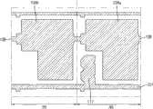
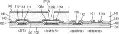
图2示出了根据本发明一实施方式的平板显示器件的有源区和外围区的像素结构,图3示出了图2沿线I-I’的横截面图。FIG. 2 shows a pixel structure of an active area and a peripheral area of a flat panel display device according to an embodiment of the present invention, and FIG. 3 shows a cross-sectional view along line I-I' of FIG. 2 .
参见图2和3,在有源区AR限定多个像素区。如图2所示,栅线101和数据线103彼此交叉设置在每一个像素区以限定单元像素区。薄膜晶体管(TFT)是开关器件,设置在栅线101和数据线103彼此交叉的区域。从TFT的漏极120延伸的第一公共电极108a、存储电极120a和像素电极150设置在像素区的里面,从而它们彼此重叠。第一公共电极108a从公共线108分支,基本平行于栅线101,横跨像素区延伸。Referring to FIGS. 2 and 3, a plurality of pixel regions are defined in the active region AR. As shown in FIG. 2 , the
公共线108具有在公共线与数据线103交叉的区域内宽度变窄的结构。提供这种变窄的结构以防止与公共线108交叉的数据线103被截断。此外,预定的栅线突出物形成于栅线101与数据线103交叉的区域,以防止数据线在数据线103形成于栅线101之上的时候被截断。如图4A所示,预定的突出物从栅线的低层部分以与栅极111从栅线延伸的方向相反的方向延伸。The
为了允许利用电泳方法驱动平板显示器件保持图像帧在很长持续时间中保持恒定,像素区的存储电容值应该很大。因此,第一公共电极108a和存储电极120a在区域中延伸以确保在像素区中足够的存储电容。即,形成存储电极120a和第一公共电极108a以占据大多数像素区。In order to allow the electrophoretic method to drive the flat panel display device to keep the image frame constant for a long time duration, the storage capacitance value of the pixel area should be large. Therefore, the first
此外,由于利用电泳方法驱动平板显示器件与其它平板显示器件相比利用高驱动电压,因此提供较大的TFT。即,对于在高驱动电压下的操作,提供具有较宽沟道W和较长沟道L的TFT(在TFT区域中的虚线示出)。在利用电泳方法驱动的平板显示器件中,当如现有技术的LCD器件一样,形成像素电极未与TFT重叠时,反射率减小,其减小了图像质量。然而,在现有技术的LCD器件中,在形成像素电极与TFT重叠的情况下,LCD液晶由TFT的沟道和像素电极异常驱动,从而减小了图像的质量。该异常驱动问题在利用电泳方法驱动的平板显示器件中也存在。In addition, since driving a flat panel display device using an electrophoretic method utilizes a high driving voltage compared to other flat panel display devices, a larger TFT is provided. That is, for operation at a high driving voltage, a TFT with a wider channel W and a longer channel L (shown by dashed lines in the TFT region) is provided. In a flat panel display device driven by an electrophoretic method, when a pixel electrode is formed not to overlap a TFT like a related art LCD device, reflectance decreases, which reduces image quality. However, in the prior art LCD device, in the case where the pixel electrode is formed to overlap the TFT, the LCD liquid crystal is abnormally driven by the channel of the TFT and the pixel electrode, thereby degrading the image quality. This abnormal driving problem also exists in a flat panel display device driven by an electrophoretic method.
当像素电极仅存在于栅线和数据线里面时,正如现有技术的LCD器件的像素区一样,减小的反射率降低了利用电泳方法驱动的平板显示器件的图像的质量。然而,当形成像素电极覆盖像素区的数据线和栅线时,寄生容量Cgs和Cgd的尺寸增加,从而由于寄生电容使得数据信号大大失真,寄生电容作为增加反冲电压(kick back voltage)ΔV的因素。当反冲电压增加,平板显示器件的图像质量减小。When the pixel electrodes exist only inside the gate and data lines, as in the pixel region of the related art LCD device, the reduced reflectivity degrades the image quality of the flat panel display device driven by the electrophoretic method. However, when forming the data line and the gate line where the pixel electrode covers the pixel area, the size of the parasitic capacitances Cgs and Cgd increases, so that the data signal is greatly distorted due to the parasitic capacitance, which acts as a factor for increasing the kick back voltage ΔV factor. When the kickback voltage increases, the image quality of the flat panel display device decreases.
为了解决上述的问题,根据本发明实施方式的电泳平板显示器件中,像素电极延伸到并与TFT、栅线和数据线之一重叠,并且介质层141插入到像素电极与TFT、栅线和数据线之一之间以最小化图像质量降级同时提高反射率。In order to solve the above problems, in the electrophoretic flat panel display device according to the embodiment of the present invention, the pixel electrode extends to and overlaps with one of the TFT, the gate line and the data line, and the
此外,通过延伸像素电极150增加像素区中的反射率,并且通过存储电容增加的尺寸使得图像帧可以保持很长时间。In addition, the reflectance in the pixel area is increased by extending the
栅线101和与栅线101交叉的虚拟数据线123限定外围区中的虚拟像素区。虚拟公共电极108b、从虚拟数据线123分支并与虚拟公共电极108b重叠的虚拟存储电极130、以及与虚拟存储电极130电连接并覆盖在外围区中的整个虚拟像素区的虚拟像素电极160设置在每一个虚拟像素区中。虚拟像素电极160沿图1的外围区延伸,并形成为单个电极。The
尽管图2所示的虚拟存储电极130以通过两个连接部分从虚拟数据线123分支的结构形成,但虚拟存储电极130不限于该结构,可以通过如图6所示的一个连接部分连接到数据线123。Although the
参见图3,当图像信号通过有源区AR的数据线103提供给像素区,在像素电极150和染料薄膜170的第二公共电极170b之间形成电场。在像素电极150和第二公共电极170b之间形成的电场移动包含在染料层170a的微囊剂中的带电粒子以实现黑色或白色图像。Referring to FIG. 3 , when an image signal is supplied to the pixel region through the
此外,为了实现黑、白和灰色中的一种,图像信号有选择地通过虚拟数据线123提供给外围区PR,从而在虚拟像素电极160和染料薄膜170的第二公共电极170b之间形成施加到染料层170a的电场。因此,在外围区实现黑、白和灰色中的一种,从而在平板显示器件装配工艺期间,缺点的影响减小。In addition, in order to realize one of black, white and gray, an image signal is selectively supplied to the peripheral region PR through the
虚拟公共电极108b从公共线108分支。提供所示第一接触孔210a用于电气连接像素电极150与存储电极120a。提供第二接触孔210b用于电气连接虚拟像素电极160与虚拟存储电极130。The dummy
尽管在图中示出了两个第一接触孔210a和第二接触孔210b,但可以形成一个、两个或更多的像第一接触孔210a和第二接触孔210b的接触孔。Although two first and
参见图2和3示出了其它细节。栅极111从栅线101分支进入像素区域,在衬底200上形成从公共线108分支的第一公共电极108a。在形成栅极111和第一公共电极108的衬底200上形成栅绝缘层102。在与栅极111对应的栅绝缘层102的一部分上形成TFT的沟道层114。从数据线103分支的数据线103、源极119,和与源极119相对的漏极120形成于沟道层114上。在与第一像素电极108a对应的栅绝缘层102的一部分上形成存储电极120a,以与第一公共电极108a重叠,其中存储电极120a与漏极120作为一个整体形成,并延伸到像素区。提供第一公共电极108a用于确保存储电极120a和第一公共电极108a之间的存储电容。See Figures 2 and 3 for additional details. The
在形成源极119和漏极120的衬底200上形成第一钝化层140。在第一钝化层140上形成介质层141和第二钝化层142。介质层141可以是诸如丙烯(acryl)的有机层,并在具体情况下,可选地为非有机层或光刻胶。在第二钝化层142上形成像素电极150,并通过第一接触孔210a连接到形成于低层部分的存储电极120a。外围区中的虚拟像素电极160通过第二接触孔210b电连接到虚拟存储电极130。A
在像素电极150上设置染料薄膜170。染料薄膜170包括接触像素电极150的染料层170a、保护染料层170a的保护薄膜170c和插入到保护薄膜170c和染料层170a之间的第二公共电极170b。染料层170a包括含有不同种类带电粒子的微囊剂,并且利用电场驱动带电粒子以反射外部光达到白色状态,或可选地吸收外部光达到黑色状态。A dye thin film 170 is disposed on the
在像素电极150和第一钝化层140之间形成介质层141和第二钝化层142以最小化在像素电极150、栅线101和数据线103之间可能产生的寄生电容。即,介质层141控制像素电极150和存储电极120a之间的距离,并具有介电常数以减小寄生电容。A
此外,第一钝化层140防止TFT电极和数据线103直接接触介质层141而导致损坏。第二钝化层142防止像素电极150直接接触介质层141而导致损坏。具体地,当介质层141为有机层的情况下,由于有机层产生的释气,直接接触介质层141的金属电极将损坏。为了防止释气的损坏,可以分别在介质层141之上和之下形成钝化层。In addition, the
因此,在根据本发明的平板显示器中,像素电极150在有源区延伸以增加反射率,从而提高图像质量,此外确保单元像素区的存储电容。Therefore, in the flat panel display according to the present invention, the
参见图4A到4D和图3描述了根据本发明一实施方式的制造方法。A manufacturing method according to an embodiment of the present invention is described with reference to FIGS. 4A to 4D and FIG. 3 .
参见图4A,在分为有源区AR和像素区PR的衬底200上形成栅线101、栅极111、公共线108、第一公共电极108a和虚拟公共电极108b。用于栅线101和公共线108的材料的示例包括Cu、Cr、Cr合金、Mo和其合金。利用含有掩膜和蚀刻工艺的光刻胶方法形成线和电极。在所示的实施方式中,公共线108和栅线101沿外围区以及有源区延伸。4A, a
当公共线108沿像素区延伸到相邻的像素区时,公共线108在公共线与数据线103交叉的区域宽度变窄。提供这种变窄的结构以防止当有栅绝缘层介入形成数据线时,数据线由于高度差被截断。When the
此外,在从栅线101以与栅极111延伸的方向相反的方向延伸的栅线101上预定的栅线突出物,以防止在随后形成数据线时,数据线由于高度差截断。形成栅极111,将预定凹槽包括在漏极和源极与栅极111交叉的区域中,以防止当形成源极和漏极时,电极由于高度差被截断。In addition, a predetermined gate line protrusion on the
如上所述,在衬底200上形成栅线101之后,在衬底200的整个区域上形成栅绝缘层102。可用于栅绝缘层102的材料的示例包括SiOx和SiNx。As described above, after the
在衬底200上形成栅线101和公共线108以及栅绝缘层102之后,在图4B示出的有源区的栅极111上形成沟道层114、源极119和漏极120、存储电极120a和数据线103。此时,可以利用衍射掩膜或半色调掩膜同时形成沟道层114、源极119和漏极120、存储电极120a和数据线103。可选地,可以使用利用两种掩膜的工艺,从而在形成源极119和漏极120和数据线103之后形成沟道层114。After forming the
接下来,虚拟数据线123和从虚拟数据线123分支的虚拟存储电极130同时形成于外围区。Next,
沟道层114包括无定形硅层和掺有高度导电杂质的n+无定形硅层。在本发明示出的实施方式中,在三电极结构中形成源极119,在二电极结构中形成对应于源极119的漏极120以确保TFT(由图4B的虚线示出)的沟道层114的理想宽度和长度。因此,源极119和漏极120形成于图4B示出的电极彼此结合(engage)的双结构中。在电极之间形成虚线所示的沟道层114。沟道层114在长度和宽度上明显大于现有技术TFT的沟道层。The
在衬底200上形成源极119和漏极120和数据线103之后,第一钝化层140、介质层141和第二钝化层142按序形成于图4C所示的衬底200的整个区域,并进行掩膜工艺以在存储电极120a和虚拟存储电极130中形成第一接触孔210a和第二接触孔210b。在此,第一钝化层140和第二钝化层142包括诸如氧化物和氮化物的无机材料以及有机材料。After forming the
介质层141可以是有机层,或可选地为无机层或光刻胶。The
如上所述形成第一和第二接触孔210a和210b之后,如图4D所示在衬底200的整个表面形成诸如铟锡氧化物(ITO)、铟锌氧化物(IZO)或无定形的ITO(a-ITO)的透明和导电材料。After forming the first and
在有源区的像素区中执行掩膜工艺形成像素电极150,并在透明导电材料的外围区形成虚拟像素电极160。A mask process is performed in the pixel area of the active area to form the
此时,像素电极150延伸以覆盖限定像素区和TFT的数据线103和栅线101。At this time, the
在整个外围区周围以整体类型的电极结构在外围区中形成虚拟像素电极160。在操作中,黑、灰或白之一的数据信号通过虚拟数据线123提供给外围区以减小平板显示期间装配工艺期间的缺点。The
图5A到5D示出了根据本发明另一实施方式的平板显示器件的制造方法的视图。制造工艺区包括图1A的像素区的TFT区、存储电容区、图1A的栅极焊盘GP和图1A的数据焊盘。5A to 5D illustrate views of a method of manufacturing a flat panel display device according to another embodiment of the present invention. The manufacturing process area includes the TFT area of the pixel area in FIG. 1A , the storage capacitor area, the gate pad GP in FIG. 1A and the data pad in FIG. 1A .
参见图2描述图5A到5D的制造方法。在衬底200上形成Cu、Cr、Cr合金、Mo及其合金之后,利用含有掩膜的光刻胶工艺构图光刻胶。如图5A所示,利用构图的光刻胶作为掩膜执行湿刻工艺以在衬底200上形成栅极111、像素区域里面的第一公共电极108a、栅线101、公共线108以及栅极焊盘190。栅极焊盘从栅线101延伸到图1的焊盘区。Referring to FIG. 2, the manufacturing method of FIGS. 5A to 5D will be described. After Cu, Cr, Cr alloys, Mo and alloys thereof are formed on the
在衬底200上形成栅极111之后,在图5B所示的衬底200的整个区域上形成栅绝缘层102。栅绝缘层102可以为SiOx层或SiNx层。After the
随后,无定形硅层、掺杂的(n+,p+)无定形硅层以及金属层按序形成在栅绝缘层102上。利用含有衍射掩膜或半色调掩膜的光刻胶方法执行构图操作,重复执行湿刻工艺和干刻工艺以在TFT的栅极111上形成沟道层114、源极119和漏极120以及数据线103。在存储电容区域中形成存储电极120a,其与漏极120作为一个整体形成,并从像素区域延伸。Subsequently, an amorphous silicon layer, a doped (n+, p+) amorphous silicon layer and a metal layer are sequentially formed on the
此时,数据焊盘191存在于数据焊盘区,半导体层114a存在于数据焊盘191和栅绝缘层102之间。At this time, the
如上所述在衬底200上形成源极119和漏极120以及数据线103之后,如图5C所示,按序在衬底200上第一钝化层140、介质层141和第二钝化层142。利用含有掩膜的光刻胶方法在存储电极120中形成第一接触孔210a。此时,移除与栅极焊盘区和数据焊盘区对应的介质层141的部分,从而在栅绝缘层102上堆叠第一钝化层140和第二钝化层142。在此,通过第一接触孔工艺露出栅极焊盘190和数据焊盘191。更具体地,在衬底200的整个表面形成第一钝化层140,并随后在衬底200的整个表面堆叠介质层141。随后执行在介质层141形成第一接触孔的工艺,并完全移除与焊盘区对应的介质层141的一部分。然后,在衬底200上形成第二钝化层142,随后执行第一接触孔工艺。After the
第一和第二钝化层140和142包括诸如氧化物和氮化物的无机材料或有机材料。介质层141可以是有机层,或可选地为无机层或光刻胶。The first and second passivation layers 140 and 142 include inorganic or organic materials such as oxides and nitrides. The
在如上所述形成第一接触孔210a之后,如图5D所示在衬底200的整个表面形成铟锡氧化物(ITO)、铟锌氧化物(IZO)或无定形的ITO(a-ITO)的透明和导电材料。After the
随后执行掩膜工艺以在有源区的像素区形成像素电极150、在栅极焊盘190上形成栅极250以及在数据焊盘191上形成数据焊盘电极260。A mask process is then performed to form the
此时,像素电极150延伸以覆盖限定像素区和TFT(参见图2)的数据线103和栅线101。At this time, the
参见图2,在整个外围区以整体类型电极结构在外围区形成虚拟像素电极160。在操作中,黑、灰或白数据信号通过虚拟数据线123提供给外围区以减小平板显示器装配工艺器件的缺点。Referring to FIG. 2, a
图6示出了根据本发明又一实施方式的平板显示器件的平面图。FIG. 6 shows a plan view of a flat panel display device according to still another embodiment of the present invention.
由于图6中的元件与图2中元件使用相同的附图标号表示相同的元件,从而省略这些元件描述。Since the elements in FIG. 6 denote the same elements with the same reference numerals as those in FIG. 2 , descriptions of these elements are omitted.
参见图6,根据的又一实施方式具有平板显示器件的像素结构的TFT包括两个栅极,即第一栅极211a和第二栅极211b。Referring to FIG. 6 , a TFT having a pixel structure of a flat panel display device according to yet another embodiment includes two gates, ie, a
TFT包括从数据线103分支的源极219、设置在第一栅极211a和第二栅极211b之间的连接电极218、部分与第二栅极211b重叠并与像素区的存储电极220a连接的漏极220。The TFT includes a
存储电极220a与漏极220作为一个整体形成。公共电极108a设置在低层部分,像素电极150设置在存储电极220a上。像素电极150延伸以覆盖限定像素区的数据线103和栅线101。由于像素电极150的功能和效果与图2中的相同,在此省略其描述。The
当通过栅线101提供驱动信号时,将驱动电压提供给TFT的第一和第二栅极211a和211b以导通TFT。通过数据线103提供的数据信号按序通过源极219、连接电极218、漏极220以及存储电极220a以提供给像素电极150。When a driving signal is supplied through the
当如上所述将数据信号提供给像素电极150,在像素电极150和形成于染料层170a上的第二公共电极170b之间形成电场以使得包含在染料层170a的微囊剂中的带电粒子工作,参见图2和图3所述。When the data signal is supplied to the
具有上述结构的TFT可以在高驱动电压下运行以提高TFT和显示器的工作特性。A TFT having the above structure can be operated at a high driving voltage to improve the operating characteristics of the TFT and display.
如上所述,根据本公开的平板显示器件延伸设置在每一个像素区的像素电极,以允许像素电极覆盖设置在像素区的数据线和栅线以确保在每一个像素区的理想容量,并增加反射率以改进图像质量。As described above, the flat panel display device according to the present disclosure extends the pixel electrode provided in each pixel area to allow the pixel electrode to cover the data line and the gate line provided in the pixel area to ensure an ideal capacity in each pixel area, and increase reflectivity to improve image quality.
此外,在平板显示器件的外围区中提供像素电极以减小平板显示器件装配工艺器件的缺点。In addition, the pixel electrodes are provided in the peripheral region of the flat panel display device to reduce the disadvantages of the device in the fabrication process of the flat panel display device.
对于本领域的技术人员来说,在不偏离本发明精神或范围的情况下,显然可以进行各种改进和变型。因此,本发明实施方式意欲覆盖所有落入在本发明的所附权利要求书及及其等效无限定的范围内的改进和变型。更具体地,更具体地,在该公开、附图和所附权利要求的范围内对主题组合配置的组成部分和/或配置进行变型和修改是可能的。除了组成部分和/或配置的变型和修改之外,对于那些本领域技术人员,可选的用途也将是显而易见的。It will be apparent to those skilled in the art that various modifications and changes can be made without departing from the spirit or scope of the invention. Therefore, the embodiments of the present invention are intended to cover all improvements and modifications within the scope of the appended claims of the present invention and their equivalents without limitation. More particularly, variations and modifications are possible in the constituent parts and/or arrangements of the subject combination arrangements within the scope of the disclosure, the drawings and the appended claims. In addition to variations and modifications in composition and/or configuration, alternative uses will also be apparent to those skilled in the art.
Claims (18)
Applications Claiming Priority (3)
| Application Number | Priority Date | Filing Date | Title |
|---|---|---|---|
| KR10-2008-0014899 | 2008-02-19 | ||
| KR1020080014899 | 2008-02-19 | ||
| KR1020080014899AKR101346921B1 (en) | 2008-02-19 | 2008-02-19 | A flat display device and method of manufacturing the same |
Publications (2)
| Publication Number | Publication Date |
|---|---|
| CN101515102Atrue CN101515102A (en) | 2009-08-26 |
| CN101515102B CN101515102B (en) | 2011-01-05 |
Family
ID=40954264
Family Applications (1)
| Application Number | Title | Priority Date | Filing Date |
|---|---|---|---|
| CN2008101764869AExpired - Fee RelatedCN101515102B (en) | 2008-02-19 | 2008-11-13 | Flat display device and method for manufacturing the same |
Country Status (4)
| Country | Link |
|---|---|
| US (2) | US8148181B2 (en) |
| KR (1) | KR101346921B1 (en) |
| CN (1) | CN101515102B (en) |
| TW (1) | TWI413842B (en) |
Cited By (12)
| Publication number | Priority date | Publication date | Assignee | Title |
|---|---|---|---|---|
| CN102103299A (en)* | 2009-12-18 | 2011-06-22 | 乐金显示有限公司 | Electrophoretic display device and method of manufacturing the same |
| CN102645811A (en)* | 2011-11-23 | 2012-08-22 | 京东方科技集团股份有限公司 | Electronic paper active substrate, manufacturing method thereof, and electronic paper display |
| CN103137630A (en)* | 2011-11-30 | 2013-06-05 | 三星显示有限公司 | Thin film transistor array substrate, method for manufacturing the thin film transistor array substrate, and organic light emitting display device |
| CN103337479A (en)* | 2013-07-05 | 2013-10-02 | 合肥京东方光电科技有限公司 | Array substrate, display device and method for manufacturing array substrate |
| CN103761935A (en)* | 2014-01-21 | 2014-04-30 | 深圳市华星光电技术有限公司 | Display panel |
| CN107272275A (en)* | 2016-04-04 | 2017-10-20 | 三星显示有限公司 | Display device |
| WO2019056465A1 (en)* | 2017-09-25 | 2019-03-28 | 武汉华星光电技术有限公司 | Virtual circuit of flat panel display device and driving circuit |
| CN109994526A (en)* | 2017-12-29 | 2019-07-09 | 乐金显示有限公司 | Electroluminescent display device |
| CN110286527A (en)* | 2019-06-25 | 2019-09-27 | 京东方科技集团股份有限公司 | Dye liquid crystal dimming panel, manufacturing method thereof and double-layer dye liquid crystal dimming panel |
| WO2019214580A1 (en)* | 2018-05-09 | 2019-11-14 | 京东方科技集团股份有限公司 | Display substrate and manufacturing method therefor, and display device |
| CN110596987A (en)* | 2019-09-30 | 2019-12-20 | 京东方科技集团股份有限公司 | Display substrate and display device |
| US12289921B2 (en) | 2021-12-13 | 2025-04-29 | Au Optronics Corporation | Display panel |
Families Citing this family (28)
| Publication number | Priority date | Publication date | Assignee | Title |
|---|---|---|---|---|
| CN101706637B (en)* | 2009-04-03 | 2011-07-13 | 深超光电(深圳)有限公司 | Pixel electrode structure with high display quality |
| KR101276749B1 (en) | 2009-08-03 | 2013-06-19 | 엘지디스플레이 주식회사 | Electrophoretic display device and manufacturing method thereof |
| KR101662135B1 (en)* | 2010-01-15 | 2016-10-05 | 삼성디스플레이 주식회사 | Electrophoretic display panel, method of manufacturing the same and electrophoretic display apparatus having the same |
| KR101127588B1 (en)* | 2010-03-09 | 2012-03-22 | 삼성모바일디스플레이주식회사 | Liquid Crystal Display Panel and Method of Manufacturing the same |
| JP6126775B2 (en)* | 2010-06-25 | 2017-05-10 | 株式会社半導体エネルギー研究所 | Display device |
| KR20120022411A (en)* | 2010-09-02 | 2012-03-12 | 삼성모바일디스플레이주식회사 | Display device and driving method thereof |
| CN102646594A (en)* | 2011-05-20 | 2012-08-22 | 京东方科技集团股份有限公司 | A kind of channel of ESD circuit and preparation method thereof |
| TWI467673B (en)* | 2011-06-09 | 2015-01-01 | Chunghwa Picture Tubes Ltd | Wiring device and display device |
| KR101341030B1 (en) | 2012-08-29 | 2013-12-13 | 엘지디스플레이 주식회사 | Organic emitting display device and method for manufacturing the same |
| KR102017204B1 (en) | 2012-11-01 | 2019-09-03 | 삼성디스플레이 주식회사 | Thin film trannsistor array panel and manufacturing method thereof |
| CN103066017A (en)* | 2012-12-28 | 2013-04-24 | 北京京东方光电科技有限公司 | Preparing method of array substrate |
| NL2012803B1 (en) | 2014-05-12 | 2016-02-24 | Hj Forever Patents B V | Electrophoretic display. |
| US9874775B2 (en)* | 2014-05-28 | 2018-01-23 | Semiconductor Energy Laboratory Co., Ltd. | Liquid crystal display device and electronic device |
| US9564458B2 (en)* | 2014-11-26 | 2017-02-07 | Shenzhen China Star Optoelectronics Technology Co., Ltd. | TFT substrates and the manufacturing method thereof |
| TWI544272B (en) | 2015-04-17 | 2016-08-01 | 元太科技工業股份有限公司 | Display device |
| KR102484885B1 (en) | 2015-12-07 | 2023-01-05 | 엘지디스플레이 주식회사 | Display device integrated with touch screen panel and method for fabricating the same |
| KR101951939B1 (en)* | 2016-08-26 | 2019-02-25 | 엘지디스플레이 주식회사 | Display Device |
| KR102538750B1 (en) | 2016-11-29 | 2023-06-02 | 엘지디스플레이 주식회사 | Liquid crystal display device |
| CN107357105A (en)* | 2017-09-05 | 2017-11-17 | 京东方科技集团股份有限公司 | A kind of array base palte, display panel, display device |
| CN109830181A (en) | 2017-11-23 | 2019-05-31 | 群创光电股份有限公司 | Display device |
| CN207424484U (en)* | 2017-11-27 | 2018-05-29 | 京东方科技集团股份有限公司 | A kind of array substrate and display device |
| CN108803173B (en)* | 2018-07-02 | 2021-08-10 | 京东方科技集团股份有限公司 | Array substrate, manufacturing method thereof and display device |
| CN110571228B (en)* | 2019-09-26 | 2022-02-01 | 京东方科技集团股份有限公司 | Array substrate, liquid crystal display panel and display device |
| CN110675804B (en)* | 2019-11-15 | 2022-09-13 | 福州京东方光电科技有限公司 | Shutdown discharge circuit, control method thereof, display panel and display device |
| CN113311623B (en)* | 2020-02-27 | 2023-11-21 | 夏普株式会社 | display panel |
| CN111427206B (en)* | 2020-03-24 | 2022-07-26 | 京东方科技集团股份有限公司 | Array substrate and display device |
| CN111584757B (en)* | 2020-05-27 | 2022-12-06 | 京东方科技集团股份有限公司 | Display mother board and manufacturing method of display substrate |
| US11856796B2 (en)* | 2021-07-16 | 2023-12-26 | Taiwan Semiconductor Manufacturing Company, Ltd. | Semiconductor memory devices and methods of manufacturing thereof |
Family Cites Families (12)
| Publication number | Priority date | Publication date | Assignee | Title |
|---|---|---|---|---|
| KR100715943B1 (en)* | 2001-01-29 | 2007-05-08 | 삼성전자주식회사 | LCD and its manufacturing method |
| TWI291072B (en)* | 2001-09-28 | 2007-12-11 | Sanyo Electric Co | Liquid crystal display unit |
| KR100858297B1 (en)* | 2001-11-02 | 2008-09-11 | 삼성전자주식회사 | Reflective-transmissive type liquid crystal display device and method of manufacturing the same |
| JP4197233B2 (en)* | 2002-03-20 | 2008-12-17 | 株式会社日立製作所 | Display device |
| KR100905470B1 (en) | 2002-11-20 | 2009-07-02 | 삼성전자주식회사 | Thin film transistor array substrate |
| KR100956338B1 (en)* | 2002-12-11 | 2010-05-06 | 삼성전자주식회사 | Thin Film Transistor Array Substrates for Thin-Ray Detectors |
| KR100745415B1 (en)* | 2002-12-27 | 2007-08-03 | 엘지.필립스 엘시디 주식회사 | Data pad portion of liquid crystal display panel and manufacturing method thereof |
| JP4239873B2 (en)* | 2003-05-19 | 2009-03-18 | セイコーエプソン株式会社 | Electro-optical device and electronic apparatus |
| JP4285158B2 (en)* | 2003-08-29 | 2009-06-24 | セイコーエプソン株式会社 | Electro-optical device and electronic apparatus |
| KR101202983B1 (en)* | 2005-09-13 | 2012-11-20 | 엘지디스플레이 주식회사 | An array substrate for trans-flective liquid crystal display device and fabrication method of the same |
| TWI320602B (en) | 2006-03-23 | 2010-02-11 | Prime View Int Co Ltd | E-ink display and method for repairing the same |
| JP2008026348A (en)* | 2006-07-18 | 2008-02-07 | Seiko Epson Corp | Electro-optical device and electronic apparatus |
- 2008
- 2008-02-19KRKR1020080014899Apatent/KR101346921B1/enactiveActive
- 2008-08-20TWTW097131836Apatent/TWI413842B/ennot_activeIP Right Cessation
- 2008-11-13CNCN2008101764869Apatent/CN101515102B/ennot_activeExpired - Fee Related
- 2008-12-30USUS12/318,519patent/US8148181B2/enactiveActive
- 2012
- 2012-02-27USUS13/406,072patent/US8410484B2/enactiveActive
Cited By (23)
| Publication number | Priority date | Publication date | Assignee | Title |
|---|---|---|---|---|
| CN102103299A (en)* | 2009-12-18 | 2011-06-22 | 乐金显示有限公司 | Electrophoretic display device and method of manufacturing the same |
| CN102645811A (en)* | 2011-11-23 | 2012-08-22 | 京东方科技集团股份有限公司 | Electronic paper active substrate, manufacturing method thereof, and electronic paper display |
| WO2013075551A1 (en)* | 2011-11-23 | 2013-05-30 | 京东方科技集团股份有限公司 | Electronic paper active substrate, manufacturing method therefor, and electronic paper display screen |
| CN102645811B (en)* | 2011-11-23 | 2014-07-02 | 京东方科技集团股份有限公司 | Electronic-paper active substrate and manufacturing method thereof and electronic-paper display screen |
| US8861065B2 (en) | 2011-11-23 | 2014-10-14 | Boe Technology Group Co., Ltd. | Electronic paper active substrate and method of forming the same and electronic paper display panel |
| CN103137630A (en)* | 2011-11-30 | 2013-06-05 | 三星显示有限公司 | Thin film transistor array substrate, method for manufacturing the thin film transistor array substrate, and organic light emitting display device |
| CN103137630B (en)* | 2011-11-30 | 2017-10-31 | 三星显示有限公司 | Thin-film transistor array base-plate, its manufacture method and oganic light-emitting display device |
| CN103337479B (en)* | 2013-07-05 | 2016-03-30 | 合肥京东方光电科技有限公司 | The manufacture method of a kind of array base palte, display unit and array base palte |
| CN103337479A (en)* | 2013-07-05 | 2013-10-02 | 合肥京东方光电科技有限公司 | Array substrate, display device and method for manufacturing array substrate |
| CN103761935A (en)* | 2014-01-21 | 2014-04-30 | 深圳市华星光电技术有限公司 | Display panel |
| US9799247B2 (en) | 2014-01-21 | 2017-10-24 | Shenzhen China Star Optoelectronics Technology Co., Ltd. | Display panel |
| WO2015109986A1 (en)* | 2014-01-21 | 2015-07-30 | 深圳市华星光电技术有限公司 | Display panel |
| CN103761935B (en)* | 2014-01-21 | 2016-01-06 | 深圳市华星光电技术有限公司 | Display panel |
| CN107272275A (en)* | 2016-04-04 | 2017-10-20 | 三星显示有限公司 | Display device |
| WO2019056465A1 (en)* | 2017-09-25 | 2019-03-28 | 武汉华星光电技术有限公司 | Virtual circuit of flat panel display device and driving circuit |
| CN109994526B (en)* | 2017-12-29 | 2023-06-23 | 乐金显示有限公司 | Electroluminescence display device |
| CN109994526A (en)* | 2017-12-29 | 2019-07-09 | 乐金显示有限公司 | Electroluminescent display device |
| WO2019214580A1 (en)* | 2018-05-09 | 2019-11-14 | 京东方科技集团股份有限公司 | Display substrate and manufacturing method therefor, and display device |
| CN110286527A (en)* | 2019-06-25 | 2019-09-27 | 京东方科技集团股份有限公司 | Dye liquid crystal dimming panel, manufacturing method thereof and double-layer dye liquid crystal dimming panel |
| CN110286527B (en)* | 2019-06-25 | 2022-04-15 | 京东方科技集团股份有限公司 | Dye liquid crystal dimming panel, manufacturing method thereof and double-layer dye liquid crystal dimming panel |
| CN110596987A (en)* | 2019-09-30 | 2019-12-20 | 京东方科技集团股份有限公司 | Display substrate and display device |
| CN110596987B (en)* | 2019-09-30 | 2023-09-08 | 京东方科技集团股份有限公司 | Display substrate and display device |
| US12289921B2 (en) | 2021-12-13 | 2025-04-29 | Au Optronics Corporation | Display panel |
Also Published As
| Publication number | Publication date |
|---|---|
| US8410484B2 (en) | 2013-04-02 |
| KR101346921B1 (en) | 2014-01-02 |
| US20120153290A1 (en) | 2012-06-21 |
| US20090206339A1 (en) | 2009-08-20 |
| CN101515102B (en) | 2011-01-05 |
| TW200937089A (en) | 2009-09-01 |
| TWI413842B (en) | 2013-11-01 |
| US8148181B2 (en) | 2012-04-03 |
| KR20090089630A (en) | 2009-08-24 |
Similar Documents
| Publication | Publication Date | Title |
|---|---|---|
| US8148181B2 (en) | Method for manufacturing flat display device | |
| JP4277874B2 (en) | Manufacturing method of electro-optical device | |
| KR100884118B1 (en) | Electro-optical devices, electronic devices, and methods of manufacturing electro-optical devices | |
| TWI464882B (en) | Thin film transistor substrate and method of manufacturing same | |
| US8810757B2 (en) | Liquid crystal display device including a light-blocking member | |
| US7787065B2 (en) | Liquid crystal display with photosensor and method of fabricating the same | |
| US8059244B2 (en) | Liquid crystal display with high aperture ratio | |
| KR20130015735A (en) | Liquid crystal display device | |
| US20080073686A1 (en) | Thin-Film Transistor Array and Method for Manufacturing the Same | |
| US8867003B2 (en) | Liquid crystal display device | |
| CN101206325A (en) | Liquid crystal display device with photosensitive element and manufacturing method thereof | |
| KR20070042249A (en) | Thin film transistor substrate, manufacturing method thereof, liquid crystal display panel having same and manufacturing method thereof | |
| US8907347B2 (en) | Thin film transistor array panel and method for manufacturing the same, and liquid crystal display | |
| CN100495182C (en) | Active matrix liquid crystal display and manufacturing method thereof | |
| US7589030B2 (en) | Liquid crystal display device and fabricating method thereof | |
| CN101165905A (en) | Thin film transistor array structure and manufacturing method thereof | |
| KR101677282B1 (en) | Thin Film Transistor Liquid Crystal Display Device And Method for fabricating thereof | |
| KR101222537B1 (en) | Liquid Crystal Display Pane And Method for Fabricating Thereof | |
| KR101376754B1 (en) | Display substrate, method of manufacturing the same and display apparatus having the same | |
| CN118466061A (en) | Display device | |
| JP2004333858A (en) | Liquid crystal display | |
| JP2000267134A (en) | Active matrix type liquid crystal display device | |
| KR20080000208A (en) | LCD and its manufacturing method | |
| KR20040062362A (en) | array panel of liquid crystal display | |
| KR20070120231A (en) | Liquid crystal display panel |
Legal Events
| Date | Code | Title | Description |
|---|---|---|---|
| C06 | Publication | ||
| PB01 | Publication | ||
| C10 | Entry into substantive examination | ||
| SE01 | Entry into force of request for substantive examination | ||
| C14 | Grant of patent or utility model | ||
| GR01 | Patent grant | ||
| CF01 | Termination of patent right due to non-payment of annual fee | ||
| CF01 | Termination of patent right due to non-payment of annual fee | Granted publication date:20110105 Termination date:20181113 |