CN101513121B - organic light emitting display - Google Patents
organic light emitting displayDownload PDFInfo
- Publication number
- CN101513121B CN101513121BCN2007800289861ACN200780028986ACN101513121BCN 101513121 BCN101513121 BCN 101513121BCN 2007800289861 ACN2007800289861 ACN 2007800289861ACN 200780028986 ACN200780028986 ACN 200780028986ACN 101513121 BCN101513121 BCN 101513121B
- Authority
- CN
- China
- Prior art keywords
- light emitting
- organic light
- dummy pattern
- layer
- emitting display
- Prior art date
- Legal status (The legal status is an assumption and is not a legal conclusion. Google has not performed a legal analysis and makes no representation as to the accuracy of the status listed.)
- Active
Links
Images


Classifications
- H—ELECTRICITY
- H05—ELECTRIC TECHNIQUES NOT OTHERWISE PROVIDED FOR
- H05B—ELECTRIC HEATING; ELECTRIC LIGHT SOURCES NOT OTHERWISE PROVIDED FOR; CIRCUIT ARRANGEMENTS FOR ELECTRIC LIGHT SOURCES, IN GENERAL
- H05B33/00—Electroluminescent light sources
- H05B33/02—Details
- H05B33/04—Sealing arrangements, e.g. against humidity
- H—ELECTRICITY
- H10—SEMICONDUCTOR DEVICES; ELECTRIC SOLID-STATE DEVICES NOT OTHERWISE PROVIDED FOR
- H10K—ORGANIC ELECTRIC SOLID-STATE DEVICES
- H10K50/00—Organic light-emitting devices
- H10K50/80—Constructional details
- H10K50/84—Passivation; Containers; Encapsulations
- H10K50/846—Passivation; Containers; Encapsulations comprising getter material or desiccants
- H—ELECTRICITY
- H10—SEMICONDUCTOR DEVICES; ELECTRIC SOLID-STATE DEVICES NOT OTHERWISE PROVIDED FOR
- H10K—ORGANIC ELECTRIC SOLID-STATE DEVICES
- H10K59/00—Integrated devices, or assemblies of multiple devices, comprising at least one organic light-emitting element covered by group H10K50/00
- H10K59/80—Constructional details
- H10K59/87—Passivation; Containers; Encapsulations
- H10K59/874—Passivation; Containers; Encapsulations including getter material or desiccant
- H—ELECTRICITY
- H10—SEMICONDUCTOR DEVICES; ELECTRIC SOLID-STATE DEVICES NOT OTHERWISE PROVIDED FOR
- H10K—ORGANIC ELECTRIC SOLID-STATE DEVICES
- H10K59/00—Integrated devices, or assemblies of multiple devices, comprising at least one organic light-emitting element covered by group H10K50/00
- H10K59/80—Constructional details
- H10K59/88—Dummy elements, i.e. elements having non-functional features
Landscapes
- Physics & Mathematics (AREA)
- Optics & Photonics (AREA)
- Electroluminescent Light Sources (AREA)
Abstract
Translated fromChineseDescription
Translated fromChinese技术领域technical field
本发明涉及一种有机发光显示器。The invention relates to an organic light emitting display.
背景技术Background technique
随着多媒体的发展,近年来平板显示器的重要性有所提高。诸如液晶显示器(LCD)、等离子体显示面板(PDP)、场致发射显示器(FED)、有机发光显示器等这样的各种平板显示器已经投入实际应用。With the development of multimedia, the importance of flat panel displays has increased in recent years. Various flat panel displays such as liquid crystal displays (LCDs), plasma display panels (PDPs), field emission displays (FEDs), organic light emitting displays, etc. have been put into practical use.
有机发光显示器具有快速的响应时间、较低的功率消耗和自发光结构。此外,有机发光显示器具有较宽的视角,从而不管屏幕的尺寸或观看者的位置如何,可出色地显示运动画面。Organic light emitting displays have fast response time, low power consumption, and self-luminous structures. In addition, the organic light emitting display has a wide viewing angle, thereby excellently displaying moving pictures regardless of the size of the screen or the position of the viewer.
因为有机发光显示器使用半导体制造工艺在低温环境中制造,所以有机发光显示器具有简单的制造工艺。因此,作为下一代显示显示器,有机发光显示器引起注意。Because the organic light emitting display is manufactured in a low temperature environment using a semiconductor manufacturing process, the organic light emitting display has a simple manufacturing process. Therefore, organic light emitting displays are attracting attention as next-generation display displays.
一般地,有机发光显示器具有以矩阵形式布置的NM有机发光二极管,并且可以是电压驱动或电流驱动的,由此显示预定的图像。有机发光显示器具有无源矩阵型驱动方式和使用薄膜晶体管的有源矩阵型驱动方式。Generally, an organic light emitting display has NM organic light emitting diodes arranged in a matrix, and may be voltage driven or current driven, thereby displaying a predetermined image. The organic light emitting display has a passive matrix type driving method and an active matrix type driving method using thin film transistors.
有机发光显示器包括多个有机发光二极管,每个有机发光二极管都具有两个电极和位于两个电极之间的有机发光层。因为有机发光层在湿气中较弱,所以有机发光显示器很容易恶化。An organic light emitting display includes a plurality of organic light emitting diodes each having two electrodes and an organic light emitting layer between the two electrodes. Organic light emitting displays are easily degraded because the organic light emitting layer is weak in moisture.
因此,可在有机发光显示器中设置用于吸收从有机发光显示器外部渗透过有机发光显示器的湿气的湿气吸收剂。Accordingly, a moisture absorbent for absorbing moisture permeating through the organic light emitting display from the outside of the organic light emitting display may be provided in the organic light emitting display.
然而,因为需要大量的湿气吸收剂来充分吸收从外部渗透的湿气,所以可能损坏有机发光层,并导致其中有机发光层的发光区域减小的像素收缩现象。However, since a large amount of moisture absorbent is required to sufficiently absorb moisture penetrating from the outside, the organic light emitting layer may be damaged and cause a pixel shrinkage phenomenon in which the light emitting area of the organic light emitting layer is reduced.
此外,在其中从外部给有机发光显示器施加压力的情形中,有机发光二极管接触湿气吸收剂。这导致对有机发光显示器的损坏。因此,在有机发光显示器的屏幕上产生污点或线缺陷,因而降低了有机发光显示器的质量和寿命。Also, in the case where pressure is applied to the organic light emitting display from the outside, the organic light emitting diode contacts the moisture absorbent. This results in damage to the organic light emitting display. Accordingly, stains or line defects are generated on the screen of the organic light emitting display, thereby reducing the quality and lifespan of the organic light emitting display.
发明内容Contents of the invention
在一个方面中,有机发光显示器包括:基板;位于所述基板上并包括多个子像素的显示部,每个子像素都包括第一电极、至少包含有机发光层的发光单元和第二电极;以及位于所述显示部的边缘的虚拟图案,该虚拟图案包括虚拟层,所述虚拟层包括与用于形成所述发光单元的多个层中的至少一个层相同的形成材料。In one aspect, an organic light-emitting display includes: a substrate; a display portion located on the substrate and including a plurality of sub-pixels, each sub-pixel including a first electrode, a light-emitting unit including at least an organic light-emitting layer, and a second electrode; A dummy pattern of an edge of the display part, the dummy pattern including a dummy layer including the same forming material as at least one of the layers used to form the light emitting unit.
因为根据典型实施方式的有机发光显示器在显示部外部包括虚拟图案,所以虚拟图案可吸收从有机发光显示器外部渗透过有机发光显示器的湿气或氧气。因此,可防止由于湿气或氧气而导致的有机发光显示器的恶化,因而可提高有机发光显示器的质量和寿命。Since the organic light emitting display according to the exemplary embodiment includes the dummy pattern outside the display part, the dummy pattern may absorb moisture or oxygen permeating through the organic light emitting display from the outside of the organic light emitting display. Accordingly, deterioration of the organic light emitting display due to moisture or oxygen can be prevented, and thus the quality and lifespan of the organic light emitting display can be improved.
附图说明Description of drawings
给本发明提供进一步理解并结合组成本说明书一部分的附图图解了本发明的实施方式并与说明书一起用于解释本发明的原理。在附图中:The accompanying drawings, which are included to provide a further understanding of the invention and constitute a part of this specification, illustrate embodiments of the invention and together with the description serve to explain the principles of the invention. In the attached picture:
图1是根据一个典型实施方式的有机发光显示器的平面图;1 is a plan view of an organic light emitting display according to an exemplary embodiment;
图2是图1的有机发光显示器的横截面图;2 is a cross-sectional view of the organic light emitting display of FIG. 1;
图3是根据一个典型实施方式的有机发光显示器的子像素的横截面图;3 is a cross-sectional view of a sub-pixel of an organic light emitting display according to an exemplary embodiment;
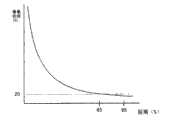
图4是显示像素收缩与虚拟图案的位置之间的关系的曲线;FIG. 4 is a graph showing the relationship between pixel shrinkage and the position of a dummy pattern;
图5是根据一个改进的典型实施方式的有机发光显示器的平面图;5 is a plan view of an organic light emitting display according to an improved exemplary embodiment;
图6是根据另一个改进的典型实施方式的有机发光显示器的平面图;6 is a plan view of an organic light emitting display according to another modified exemplary embodiment;
图7是根据另一个改进的典型实施方式的有机发光显示器的平面图。FIG. 7 is a plan view of an organic light emitting display according to another modified exemplary embodiment.
具体实施方式Detailed ways
现在将详细描述附图中图解的本发明的实施方式。Embodiments of the present invention illustrated in the accompanying drawings will now be described in detail.
图1是根据一个典型实施方式的有机发光显示器的平面图。图2是图1的有机发光显示器的横截面图。FIG. 1 is a plan view of an organic light emitting display according to an exemplary embodiment. FIG. 2 is a cross-sectional view of the organic light emitting display of FIG. 1 .
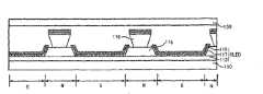
如图1和2中所示,根据一个典型实施方式的有机发光显示器100包括第一基板110、位于第一基板110上的显示部P、虚拟图案130、密封区域140和第二基板150。As shown in FIGS. 1 and 2 , an organic
第一基板110包括诸如玻璃这样的透明材料、诸如塑料这样的柔性材料、或者金属材料。The
显示部P包括多个子像素120,每个子像素120都包括第一电极、有机发光单元和第二电极。根据有机发光单元的形成材料,每个子像素120可发射红色、绿色、蓝色或白色光。The display part P includes a plurality of
图3是根据一个典型实施方式的有机发光显示器的子像素的横截面图。FIG. 3 is a cross-sectional view of a sub-pixel of an organic light emitting display according to an exemplary embodiment.
如图3中所示,第一电极113位于第一基板110上。第一电极113可为阳极电极。第一电极113可包括诸如氧化铟锡(ITO)层这样的透明导电氧化物层。在第一电极113上设有堤岸层(bank layer)115,以在第一电极113之间提供电绝缘并确定发光区域。由堤岸层115暴露的第一电极113的区域定义为发光区域E。第一电极113的除发光区域E之外的其他区域定义为非发光区域N。As shown in FIG. 3 , the
在堤岸层115上设有倒梯形隔板116,在由堤岸层115暴露的第一电极113的区域(即发光区域E)上设有发光单元117。发光单元117包括有机发光层以及位于有机发光层上和下的空穴注入层、空穴传输层、电子传输层和电子注入层中的至少一个。An inverted
在发光单元117上设有第二电极119。第二电极119可为阴极电极。隔板116在第二电极119之间而将第二电极119彼此隔开。第二电极119包括具有低功率函数和出色反射率的材料,如铝(Al)、镁(Mg)和银(Ag)。The
发光单元117从第一电极115接收空穴,并从第二电极119接收电子,从而形成电子空穴对。然后,由于当电子空穴对返回到基级时产生的光,有机发光显示器显示图像。The
在有源矩阵型有机发光显示器中,每个子像素120可进一步包括与第一电极113电连接的薄膜晶体管。In an active matrix organic light emitting display, each
参照图1和2,虚拟图案130位于显示部P的边缘处。虚拟图案130包括虚拟层,该虚拟层包含有机材料或无机材料。虚拟层可包括用于形成子像素120的发光单元117的多个层中的任意一个。例如,虚拟层可包括空穴注入层、空穴传输层、有机发光层、电子传输层或电子注入层中的一个。Referring to FIGS. 1 and 2 , a
虚拟图案130可包括多个虚拟层。换句话说,虚拟图案130可包括空穴注入层、空穴传输层、有机发光层、电子传输层或电子注入层中的至少一个。虚拟层可包括有机材料和无机材料。The
因为形成虚拟图案130的虚拟层的有机材料或无机材料可与从有机发光显示器外部渗透过有机发光显示器的湿气或氧气反应,所以由于通过在溶剂中溶解一种或多种溶质而获得的具有预定溶解性的固溶体,虚拟层可吸收湿气或氧气。Since the organic material or inorganic material forming the dummy layer of the
因此,因为虚拟层吸收有机发光显示器中存在的湿气或氧气,所以可防止有机发光层的恶化。Accordingly, since the dummy layer absorbs moisture or oxygen present in the organic light emitting display, deterioration of the organic light emitting layer may be prevented.
虚拟图案130可进一步包括金属层。更具体地说,金属层位于虚拟图案130内部,并包括在虚拟层上的与第二电极相同的形成材料。在金属层位于虚拟层上的情形中,金属层可防止吸收湿气或氧气的虚拟层的脱落。The
尽管图中没有示出,但虚拟图案130可进一步包括位于虚拟层下的绝缘层。该绝缘层可包括与位于子像素120的第一电极113上的堤岸层115相同的形成材料。Although not shown in the drawing, the
如上所述,使用与子像素120相同的形成工艺可形成包括虚拟层、金属层或绝缘层的虚拟图案130。例如,当制造子像素120的有机发光层时,通过在与虚拟图案130的位置对应的掩模区域上形成开口区域,可将虚拟图案130构图为具有各种尺寸和形式。As described above, the
虚拟图案130的金属层和子像素120的第二电极可同时形成。虚拟图案130的绝缘层和子像素120的堤岸层可同时形成。The metal layer of the
因为虚拟图案130和子像素120同时形成,所以不需要用于形成虚拟图案130的单独工艺。Since the
密封区域140位于显示部P的边缘处,与虚拟图案130隔开预定的距离。在密封区域140上涂敷有密封剂,以将第一基板110粘附到第二基板150。The sealing
第二基板150一般由金属帽、透明或不透明玻璃基板、或保护膜等形成,然而,典型的实施方式并不限于此。可在第二基板150内形成吸收湿气和氧气的湿气吸收剂170。The
虚拟图案130可更靠近密封区域140而不是更靠近所述显示部。更具体地说,虚拟图案130位于与从显示部P到密封区域140的距离的65-95%对应的位置处。当虚拟图案130位于与等于或大于所述距离的65%对应的位置处时,虚拟图案130靠近密封区域140,由此可有效吸收从外部渗透过的湿气或氧气。此外,当虚拟图案130位于与等于或小于所述距离的95%对应的位置处时,虚拟图案130的虚拟层可防止密封区域140的污染,并提高了第一基板110与第二基板150之间的粘结强度。The
图4是显示像素收缩与虚拟图案的位置之间的关系的曲线。FIG. 4 is a graph showing the relationship between pixel shrinkage and the position of a dummy pattern.
如图4中所示,当虚拟图案130位于与从显示部P到密封区域140的距离的65-95%对应的位置处时,像素收缩保持在大约20%的水平。As shown in FIG. 4, when the
图5到图7是根据改进的典型实施方式的有机发光显示器的平面图。5 to 7 are plan views of an organic light emitting display according to a modified exemplary embodiment.
如图5中所示,使用与形成在基板210上的发光单元220相同的形成工艺形成虚拟图案230。具有与发光单元220相同尺寸或形状的多个虚拟图案230形成为包围显示部P。虚拟图案230的尺寸可大于发光单元220的尺寸。如上,当虚拟图案230为多个时,该多个虚拟图案230可有效吸收渗透过显示部P的外围区域的湿气或氧气。As shown in FIG. 5 , the dummy pattern 230 is formed using the same formation process as that of the light emitting unit 220 formed on the substrate 210 . A plurality of dummy patterns 230 having the same size or shape as the light emitting unit 220 are formed to surround the display part P. Referring to FIG. The size of the dummy pattern 230 may be larger than that of the light emitting unit 220 . As above, when there are a plurality of dummy patterns 230, the plurality of dummy patterns 230 can effectively absorb moisture or oxygen permeating through the peripheral area of the display part P. Referring to FIG.
如图6中所示,虚拟图案330可包括形成在基板310上的位于显示部P与密封区域340之间的第一和第二虚拟图案330a和330b。第一虚拟图案330a形成在显示部P与密封区域340之间的每个角落处,第二虚拟图案330b形成在显示部P与密封区域340之间的直线区域中。因为渗透过显示部P与密封区域340之间的角落的湿气或氧气的量大于渗透过其他区域的湿气或氧气的量,所以第一虚拟图案330a的宽度大于第二虚拟图案330b的宽度。As shown in FIG. 6 , the
如图7中所示,虚拟图案430形成在显示部P与密封区域440之间的区域的一侧或两侧,从而不影响扫描线或数据线的形成。As shown in FIG. 7, the
在本发明的实施方式中可进行各种改进和变化,这对于本领域技术人员来说是显而易见的。因而,本发明意在覆盖落入所附权利要求及其等价物范围内的这里所述实施方式的改进和变化。It will be apparent to those skilled in the art that various modifications and changes can be made in the embodiments of the present invention. Thus, it is intended that the present invention covers the modifications and variations of the embodiments described herein which come within the scope of the appended claims and their equivalents.
工业实用性Industrial Applicability
如上,因为根据典型实施方式的有机发光显示器在显示部外部包括虚拟图案,所以虚拟图案可吸收从有机发光显示器外部渗透过有机发光显示器的湿气或氧气。As above, since the organic light emitting display according to the exemplary embodiment includes the dummy pattern outside the display part, the dummy pattern may absorb moisture or oxygen permeating through the organic light emitting display from the outside of the organic light emitting display.
因此,可防止由于湿气或氧气而导致的有机发光显示器的恶化,因而可提高有机发光显示器的质量和寿命。从而根据典型实施方式的有机发光显示器具有工业实用性。Accordingly, deterioration of the organic light emitting display due to moisture or oxygen can be prevented, and thus the quality and lifespan of the organic light emitting display can be improved. Thus, the organic light emitting display according to the exemplary embodiments has industrial applicability.
Claims (11)
Translated fromChineseApplications Claiming Priority (4)
| Application Number | Priority Date | Filing Date | Title |
|---|---|---|---|
| KR1020060073525 | 2006-08-03 | ||
| KR20060073525 | 2006-08-03 | ||
| KR10-2006-0073525 | 2006-08-03 | ||
| PCT/KR2007/003747WO2008016279A1 (en) | 2006-08-03 | 2007-08-03 | Organic light emitting device |
Publications (2)
| Publication Number | Publication Date |
|---|---|
| CN101513121A CN101513121A (en) | 2009-08-19 |
| CN101513121Btrue CN101513121B (en) | 2010-10-20 |
Family
ID=38997414
Family Applications (1)
| Application Number | Title | Priority Date | Filing Date |
|---|---|---|---|
| CN2007800289861AActiveCN101513121B (en) | 2006-08-03 | 2007-08-03 | organic light emitting display |
Country Status (3)
| Country | Link |
|---|---|
| US (1) | US8198624B2 (en) |
| CN (1) | CN101513121B (en) |
| WO (1) | WO2008016279A1 (en) |
Families Citing this family (6)
| Publication number | Priority date | Publication date | Assignee | Title |
|---|---|---|---|---|
| KR101082293B1 (en)* | 2009-09-04 | 2011-11-09 | 삼성모바일디스플레이주식회사 | Touch Screen Panel |
| KR101811341B1 (en)* | 2010-12-09 | 2017-12-26 | 삼성디스플레이 주식회사 | Organic light emitting diode display |
| JP2014154566A (en)* | 2013-02-04 | 2014-08-25 | Toshiba Corp | Organic electroluminescent element, illumination device and illumination system |
| KR102280162B1 (en)* | 2014-08-31 | 2021-07-20 | 엘지디스플레이 주식회사 | Organic light emitting diode display panel |
| KR102332255B1 (en)* | 2015-04-29 | 2021-11-29 | 삼성디스플레이 주식회사 | Display device |
| KR20170012707A (en)* | 2015-07-22 | 2017-02-03 | 삼성디스플레이 주식회사 | Flexible organic light emitting display device |
Citations (2)
| Publication number | Priority date | Publication date | Assignee | Title |
|---|---|---|---|---|
| CN1514679A (en)* | 2002-12-31 | 2004-07-21 | Lg.������Lcd����˾ | Electroluminescent display device and method and apparatus for manufacturing the same |
| US6784459B2 (en)* | 2000-11-27 | 2004-08-31 | Seiko Epson Corporation | Organic electroluminescent device, manufacturing method therefor, and electronic devices therewith |
Family Cites Families (8)
| Publication number | Priority date | Publication date | Assignee | Title |
|---|---|---|---|---|
| JP4173722B2 (en)* | 2002-11-29 | 2008-10-29 | 三星エスディアイ株式会社 | Vapor deposition mask, organic EL element manufacturing method using the same, and organic EL element |
| JP4138672B2 (en)* | 2003-03-27 | 2008-08-27 | セイコーエプソン株式会社 | Manufacturing method of electro-optical device |
| KR100522693B1 (en)* | 2003-07-12 | 2005-10-19 | 삼성에스디아이 주식회사 | Organic electro luminescence display device |
| JP2005190779A (en)* | 2003-12-25 | 2005-07-14 | Hitachi Displays Ltd | Display device |
| KR100663028B1 (en)* | 2003-12-30 | 2006-12-28 | 엘지.필립스 엘시디 주식회사 | Organic electroluminescent device and manufacturing method thereof |
| JP3951055B2 (en)* | 2004-02-18 | 2007-08-01 | セイコーエプソン株式会社 | Organic electroluminescence device and electronic device |
| KR100623451B1 (en)* | 2004-09-14 | 2006-09-19 | 엘지전자 주식회사 | Organic electroluminescent display device and manufacturing method thereof |
| KR20060117034A (en)* | 2005-05-12 | 2006-11-16 | 삼성전자주식회사 | Display device and manufacturing method thereof |
- 2007
- 2007-08-03USUS12/376,050patent/US8198624B2/enactiveActive
- 2007-08-03WOPCT/KR2007/003747patent/WO2008016279A1/enactiveApplication Filing
- 2007-08-03CNCN2007800289861Apatent/CN101513121B/enactiveActive
Patent Citations (2)
| Publication number | Priority date | Publication date | Assignee | Title |
|---|---|---|---|---|
| US6784459B2 (en)* | 2000-11-27 | 2004-08-31 | Seiko Epson Corporation | Organic electroluminescent device, manufacturing method therefor, and electronic devices therewith |
| CN1514679A (en)* | 2002-12-31 | 2004-07-21 | Lg.������Lcd����˾ | Electroluminescent display device and method and apparatus for manufacturing the same |
Also Published As
| Publication number | Publication date |
|---|---|
| CN101513121A (en) | 2009-08-19 |
| WO2008016279A1 (en) | 2008-02-07 |
| US8198624B2 (en) | 2012-06-12 |
| US20090267059A1 (en) | 2009-10-29 |
Similar Documents
| Publication | Publication Date | Title |
|---|---|---|
| CN100413115C (en) | Organic Electroluminescent Devices | |
| JP4365364B2 (en) | Organic electroluminescent device and manufacturing method thereof | |
| JP4964605B2 (en) | Manufacturing method of organic EL display device | |
| CN108400154B (en) | OLED panel | |
| US8093804B2 (en) | Organic electroluminescent display device having a novel concept for luminous efficiency | |
| CN109411619A (en) | OLED array and preparation method thereof, display panel and display device | |
| KR20060025317A (en) | Organic electroluminescent device and manufacturing method thereof | |
| CN100565903C (en) | Organic electroluminescent display device and method of fabricating the same | |
| CN101513121B (en) | organic light emitting display | |
| KR20050111163A (en) | Organic electro-luminescence display device and method for fabricating thereof | |
| KR101001423B1 (en) | Organic electroluminescent device and manufacturing method thereof | |
| KR101752318B1 (en) | Method of fabricating Organic electro luminescent device | |
| JP2008288034A (en) | Organic electroluminescent display device | |
| KR100717327B1 (en) | Organic electroluminescence display device and manufacturing method thereof | |
| KR100631121B1 (en) | Organic light emitting display device and manufacturing method thereof | |
| KR100749490B1 (en) | Organic electroluminescent display and manufacturing method thereof | |
| KR101595471B1 (en) | Organic Electroluminescence Device and Method for fabricating the same | |
| KR100638139B1 (en) | Organic electroluminescent display device and manufacturing method thereof | |
| KR100616706B1 (en) | Organic electroluminescent device and manufacturing method thereof | |
| KR100623450B1 (en) | Organic electroluminescent display device and manufacturing method thereof | |
| JP2008288031A (en) | El display device | |
| KR100726954B1 (en) | Organic light emitting display device and manufacturing method | |
| KR100641733B1 (en) | Organic electroluminescent display device and manufacturing method thereof | |
| KR100726943B1 (en) | Organic electroluminescent display and manufacturing method | |
| KR20050104100A (en) | Organic electro luminescence device and fabrication method thereof |
Legal Events
| Date | Code | Title | Description |
|---|---|---|---|
| C06 | Publication | ||
| PB01 | Publication | ||
| C10 | Entry into substantive examination | ||
| SE01 | Entry into force of request for substantive examination | ||
| C14 | Grant of patent or utility model | ||
| GR01 | Patent grant |