CN101512663B - Method and apparatus for reading multi-level passive element memory cell array - Google Patents
Method and apparatus for reading multi-level passive element memory cell arrayDownload PDFInfo
- Publication number
- CN101512663B CN101512663BCN2007800330616ACN200780033061ACN101512663BCN 101512663 BCN101512663 BCN 101512663BCN 2007800330616 ACN2007800330616 ACN 2007800330616ACN 200780033061 ACN200780033061 ACN 200780033061ACN 101512663 BCN101512663 BCN 101512663B
- Authority
- CN
- China
- Prior art keywords
- data
- bit line
- reference current
- reads
- value
- Prior art date
- Legal status (The legal status is an assumption and is not a legal conclusion. Google has not performed a legal analysis and makes no representation as to the accuracy of the status listed.)
- Active
Links
Images


Classifications
- G—PHYSICS
- G11—INFORMATION STORAGE
- G11C—STATIC STORES
- G11C11/00—Digital stores characterised by the use of particular electric or magnetic storage elements; Storage elements therefor
- G11C11/56—Digital stores characterised by the use of particular electric or magnetic storage elements; Storage elements therefor using storage elements with more than two stable states represented by steps, e.g. of voltage, current, phase, frequency
- G—PHYSICS
- G11—INFORMATION STORAGE
- G11C—STATIC STORES
- G11C13/00—Digital stores characterised by the use of storage elements not covered by groups G11C11/00, G11C23/00, or G11C25/00
- G11C13/0002—Digital stores characterised by the use of storage elements not covered by groups G11C11/00, G11C23/00, or G11C25/00 using resistive RAM [RRAM] elements
- G11C13/0021—Auxiliary circuits
- G11C13/004—Reading or sensing circuits or methods
- G—PHYSICS
- G11—INFORMATION STORAGE
- G11C—STATIC STORES
- G11C13/00—Digital stores characterised by the use of storage elements not covered by groups G11C11/00, G11C23/00, or G11C25/00
- G11C13/0002—Digital stores characterised by the use of storage elements not covered by groups G11C11/00, G11C23/00, or G11C25/00 using resistive RAM [RRAM] elements
- G11C13/0021—Auxiliary circuits
- G11C13/0069—Writing or programming circuits or methods
- G—PHYSICS
- G11—INFORMATION STORAGE
- G11C—STATIC STORES
- G11C13/00—Digital stores characterised by the use of storage elements not covered by groups G11C11/00, G11C23/00, or G11C25/00
- G11C13/0002—Digital stores characterised by the use of storage elements not covered by groups G11C11/00, G11C23/00, or G11C25/00 using resistive RAM [RRAM] elements
- G11C13/0021—Auxiliary circuits
- G11C13/004—Reading or sensing circuits or methods
- G11C2013/0054—Read is performed on a reference element, e.g. cell, and the reference sensed value is used to compare the sensed value of the selected cell
- G—PHYSICS
- G11—INFORMATION STORAGE
- G11C—STATIC STORES
- G11C13/00—Digital stores characterised by the use of storage elements not covered by groups G11C11/00, G11C23/00, or G11C25/00
- G11C13/0002—Digital stores characterised by the use of storage elements not covered by groups G11C11/00, G11C23/00, or G11C25/00 using resistive RAM [RRAM] elements
- G11C13/0021—Auxiliary circuits
- G11C13/0069—Writing or programming circuits or methods
- G11C2013/009—Write using potential difference applied between cell electrodes
- G—PHYSICS
- G11—INFORMATION STORAGE
- G11C—STATIC STORES
- G11C2213/00—Indexing scheme relating to G11C13/00 for features not covered by this group
- G11C2213/70—Resistive array aspects
- G11C2213/77—Array wherein the memory element being directly connected to the bit lines and word lines without any access device being used
Landscapes
- Engineering & Computer Science (AREA)
- Computer Hardware Design (AREA)
- Semiconductor Memories (AREA)
- Read Only Memory (AREA)
Abstract
Description
Translated fromChinese技术领域technical field
本发明涉及包含可编程多级存储器单元阵列的半导体集成电路,且特定来说涉及并入有无源元件存储器单元的那些阵列,且更特定来说涉及具有三维存储器阵列的那些集成电路。The present invention relates to semiconductor integrated circuits comprising arrays of programmable multi-level memory cells, and particularly to those arrays incorporating passive element memory cells, and more particularly to those integrated circuits having three-dimensional memory arrays.
背景技术Background technique
由于需要多个写入循环及多个读取循环,因此用存储在每一单元中的两个以上级来写入及读取存储器单元导致性能损失。在3D无源元件阵列中,由于这些阵列中的其它性能限制,此是特殊问题。Writing and reading memory cells with more than two stages stored in each cell results in a performance penalty because multiple write cycles and multiple read cycles are required. In 3D passive element arrays, this is a particular problem due to other performance limitations in these arrays.
已说明了其它多级存储器单元,尤其是具有电荷存储层(例如,浮动栅极)的三端子装置。在这些装置中,存储器单元的栅极端子通常耦合到字线,且通过在所述字线上应用不同的电压来读取各种存储器状态。在每一此种字线电压下,如果所述字线电压高于所编程的阈值电压,那么电流在位线上流动且被感测。Other multi-level memory cells have been described, particularly three-terminal devices with charge storage layers (eg, floating gates). In these devices, the gate terminals of the memory cells are typically coupled to a word line, and various memory states are read by applying different voltages on the word line. At each such word line voltage, if the word line voltage is above the programmed threshold voltage, current flows on the bit line and is sensed.
某些无源元件存储器单元展示可重新写入的特性。举例来说,在某些存储器单元中,可通过用约6-8V的电压正向偏置存储器单元(例如,参考其之间二极管的极性)来实现编程,而通过用约10-14V的电压反向偏置存储器单元来实现擦除。Certain passive element memory cells exhibit re-writable properties. For example, in some memory cells, programming can be achieved by forward biasing the memory cell (e.g., with reference to the polarity of a diode between them) with a voltage of about 6-8 V, and by using a voltage of about 10-14 V The voltage reverse biases the memory cell to enable erasure.
发明内容Contents of the invention
在具有最低有效位(LSB)及最高有效位(MSB)的四级无源元件单元中,某人传统上将必须以三个指数步进的电流(即,Iref)级感测来在四个状态之间进行区别。在每一此种感测操作之间,存在必需的延迟来稳定位线(其通常是高电容性负载的节点)上的电流级,因此可能需要三个长读取循环。In a four-level passive element cell with least significant bit (LSB) and most significant bit (MSB), one would traditionally have to sense with three exponentially stepped current (i.e., Iref) levels to switch between four distinguish between states. Between each such sensing operation, there is a delay necessary to stabilize the current level on the bit line (which is usually a highly capacitively loaded node), so three long read cycles may be required.
相反,可将LSB映射为一个页的部分,且将MSB映射为另一页的部分。此外,以灰度方式指派数据状态,其中向最高电阻状态(即,“未爆裂(un-popped)”状态)指派11状态,且向最低电阻状态(即,“爆裂(popped)”状态)指派10状态。因此,仅需要中级读取参考来读取LSB。可选择其它两个数据状态的状态指派,使得LSB的中级读取参考不依赖于MSB。优选地,所述其它两个数据状态具有在“爆裂”10状态与“未爆裂”11状态之间的电阻,其中向更接近所述“爆裂”10状态的数据状态指派所述00状态,且向更接近所述“未爆裂”11状态的数据状态指派所述01状态。当读取MSB时,可使用所述10与00数据状态之间的第一参考及01与11数据状态之间的第二参考,且不需要使用中级参考。Instead, the LSB may be mapped as part of one page and the MSB as part of another page. Furthermore, the data states are assigned in a grayscale fashion, with the 11 state assigned to the highest resistance state (i.e., the "un-popped" state) and the lowest resistance state (i.e., the "popped" state) 10 states. Therefore, only the mid-level read reference is needed to read the LSB. The state assignments for the other two data states can be chosen such that the intermediate read reference of the LSB is not dependent on the MSB. Preferably, said other two data states have a resistance between a "bursted" 10 state and an "unbursted" 11 state, wherein said 00 state is assigned to the data state closer to said "bursted" 10 state, and The 01 state is assigned to a data state that is closer to the "unbursted" 11 state. When reading the MSB, the first reference between the 10 and 00 data states and the second reference between the 01 and 11 data states can be used, and there is no need to use intermediate references.
一般来说,本发明涉及用于读取多级无源元件存储器单元阵列的设备,且涉及用于读取多级无源元件存储器单元阵列的方法。然而,本发明由所附权利要求书界定,且不应将此部分中的任何东西视为限制那些权利要求。In general, the present invention relates to apparatus for reading multi-level passive element memory cell arrays, and to methods for reading multi-level passive element memory cell arrays. However, the invention is defined by the appended claims, and nothing in this section should be taken as limiting those claims.
在一个方面中,本发明提供一种集成电路,其包括:(a)存储器阵列,其包含具有分别对应于逐渐降低的第一、第二、第三及第四电阻级的第一、第二、第三及第四存储器单元状态的多级无源元件存储器单元;及(b)区分构件,其用于通过针对参考电流级与选定位线上的读取偏压的至少两个不同组合感测所述选定位线上的电流来在存储器单元状态之间进行区分。In one aspect, the present invention provides an integrated circuit comprising: (a) a memory array including first, second , multi-level passive element memory cells for third and fourth memory cell states; and (b) distinguishing means for sensing by at least two different combinations for a reference current level and a read bias voltage on a selected bit line The current on the selected bit line is measured to distinguish between memory cell states.
在另一方面中,本发明提供一种集成电路,其包括:(a)存储器阵列,其包含具有分别对应于逐渐降低的第一、第二、第三及第四电阻级的第一、第二、第三及第四存储器单元状态的多级无源元件存储器单元;(b)位线偏置电路,其经配置以用读取偏压来偏置选定位线;(c)字线偏置电路,其经配置以用选定字线电压来偏置选定字线;(d)感测电路,其经配置以产生分别表示所述选定位线上的相对于第一参考电流级及相对于第二参考电流级的电流的第一信号及第二信号;及(e)数据形成电路,其经配置以依据所述第一及第二信号来产生第一数据位的读取数据值。In another aspect, the present invention provides an integrated circuit comprising: (a) a memory array including first, second Two, multi-level passive element memory cells of the third and fourth memory cell states; (b) a bit line bias circuit configured to bias a selected bit line with a read bias; (c) a word line bias a set circuit configured to bias a selected word line with a selected word line voltage; (d) a sense circuit configured to generate current levels representing the selected bit lines relative to a first reference current level and a first signal and a second signal relative to a current of a second reference current level; and (e) a data forming circuit configured to generate a read data value for a first data bit in dependence on the first and second signals .
在再一方面中,本发明提供一种集成电路,其包括:(a)存储器阵列,其包含具有分别对应于逐渐降低的第一、第二、第三及第四电阻级的第一、第二、第三及第四存储器单元状态的多级无源元件存储器单元;(b)字线偏置电路,其经配置以用选定字线电压来偏置选定字线;(c)位线偏置电路,其经配置以有时用第一读取偏压来偏置选定位线,且有时用第二读取偏压来偏置所述选定位线;(d)感测电路,其经配置以产生表示在以所述第一读取偏压偏置时所述选定位线上的相对于第一参考电流级的电流的第一信号,且产生表示在以所述第二读取偏压偏置时所述选定位线上的相对于第二参考电流级的电流的第二信号;及(e)数据形成电路,其经配置以依据所述第一及第二信号来产生第一数据位的读取数据值。In yet another aspect, the present invention provides an integrated circuit comprising: (a) a memory array including first, second Two, multi-level passive element memory cells of the third and fourth memory cell states; (b) a word line bias circuit configured to bias a selected word line with a selected word line voltage; (c) bit a line bias circuit configured to sometimes bias a selected bit line with a first read bias voltage and to sometimes bias the selected bit line with a second read bias voltage; (d) a sensing circuit that configured to generate a first signal representative of a current on the selected bit line relative to a first reference current level when biased at the first read bias voltage, and to generate a signal representative of current at the selected bit line when biased at the second read bias voltage a second signal of a current on the selected bit line relative to a second reference current level when biased; and (e) a data forming circuit configured to generate a first signal based on the first and second signals The read data value of one data bit.
在另一方面中,本发明提供一种用于读取具有分别对应于逐渐降低的第一、第二、第三及第四电阻级的第一、第二、第三及第四存储器单元状态的多级无源元件存储器单元的方法。所述方法包括通过针对参考电流级与选定位线上的读取偏压的至少两个不同组合感测所述选定位线上的电流来在存储器单元状态之间进行区分。In another aspect, the present invention provides a method for reading memory cells having first, second, third and fourth states corresponding to progressively lower first, second, third and fourth resistance levels, respectively. method for multi-level passive-element memory cells. The method includes differentiating between memory cell states by sensing a current on a selected bit line for at least two different combinations of a reference current level and a read bias voltage on the selected bit line.
在另一方面中,本发明提供一种用于读取具有分别对应于逐渐降低的第一、第二、第三及第四电阻级的第一、第二、第三及第四存储器单元状态的多级无源元件存储器单元的方法。所述方法包括用读取偏压来偏置选定位线,用选定字线电压来偏置选定字线,产生分别表示所述选定位线上的相对于第一参考电流级及相对于第二参考电流级的电流的第一信号及第二信号,及依据所述第一及第二信号来产生第一数据位的读取数据值。In another aspect, the present invention provides a method for reading memory cells having first, second, third and fourth states corresponding to progressively lower first, second, third and fourth resistance levels, respectively. method for multi-level passive-element memory cells. The method includes biasing a selected bit line with a read bias voltage, biasing a selected word line with a selected word line voltage, generating current levels representing current levels on the selected bit lines relative to a first reference current level and relative to a current level relative to a first reference current level, respectively. The first signal and the second signal of the current of the second reference current level, and the read data value of the first data bit is generated according to the first and second signals.
在另一方面中,本发明提供一种用于读取具有分别对应于第一、第二、第三及第四逐渐降低电阻级的第一、第二、第三及第四存储器单元状态的多级无源元件存储器单元的方法。所述方法包括(a)用选定字线电压来偏置选定字线;(b)用第一读取偏压来偏置选定位线;(c)产生表示在以所述第一读取偏压偏置时所述选定位线上的相对于第一参考电流级的电流的第一信号;(d)用第二读取偏压来偏置所述选定位线;(e)产生表示在以所述第二读取偏压偏置时所述选定位线上的相对于第二参考电流级的电流的第二信号;及(f)依据所述第一及第二信号来确定第一数据位的读取数据值。In another aspect, the present invention provides a method for reading memory cells having first, second, third and fourth states corresponding to first, second, third and fourth gradually decreasing resistance levels, respectively. Methodology for multi-level passive element memory cells. The method includes (a) biasing a selected word line with a selected word line voltage; (b) biasing the selected bit line with a first read bias voltage; (c) generating taking a first signal of a current on said selected bitline relative to a first reference current level when biased; (d) biasing said selected bitline with a second read bias; (e) generating a second signal representing a current on the selected bit line relative to a second reference current level when biased with the second read bias voltage; and (f) determined from the first and second signals The read data value for the first data bit.
在再一方面中,本发明提供一种用于制造存储器产品的方法。所述方法包括形成存储器阵列,所述存储器阵列包含具有分别对应于逐渐降低的第一、第二、第三及第四电阻级的第一、第二、第三及第四存储器单元状态的多级无源元件存储器单元。所述方法进一步包括形成数据电路,所述数据电路经配置以通过针对参考电流级与选定位线上的读取偏压的至少两个不同组合感测所述选定位线上的电流来在存储器单元状态之间进行区分。In yet another aspect, the present invention provides a method for manufacturing a memory product. The method includes forming a memory array including multiple memory cell states having first, second, third and fourth memory cell states corresponding to first, second, third and fourth progressively lower resistance levels, respectively. level passive component memory cells. The method further includes forming a data circuit configured to generate data in the memory by sensing a current on a selected bit line for at least two different combinations of a reference current level and a read bias voltage on the selected bit line. A distinction is made between cell states.
呈若干方面的本发明适合于具有存储器阵列的集成电路,适合于用于操作此类集成电路及存储器阵列的方法,适合于并入有此类集成电路及存储器阵列的系统及装置,且适合于此类系统、装置、集成电路或存储器阵列的计算机可读媒体编码,所有这些如本文中更加详细地说明且如所附权利要求书中所论述。可单独或以组合形式使用所说明的技术、结构及方法。The invention, in its several aspects, is applicable to integrated circuits having memory arrays, to methods for operating such integrated circuits and memory arrays, to systems and devices incorporating such integrated circuits and memory arrays, and to A computer readable medium encoding such a system, apparatus, integrated circuit, or memory array, all as described in more detail herein and as discussed in the appended claims. The illustrated techniques, structures and methods can be used alone or in combination.
以上是概述,且因此必然包含对细节的简化、一般化及省略。因此,所属技术领域中的技术人员应了解,以上概述仅为说明性,且其并不打算以任何方式限制本发明。根据下文所述的详细说明,可明了本发明的其它方面、发明性特征及优点,这些方面、发明性特征及优点仅由权利要求书来界定。The foregoing is an overview and, as such, necessarily contains simplifications, generalizations, and omissions of detail. Accordingly, those skilled in the art should appreciate that the above summary is illustrative only and that it is not intended to limit the invention in any way. Other aspects, inventive features, and advantages of the present invention will become apparent from the detailed description set forth hereinafter, and are defined only by the claims.
附图说明Description of drawings
所属技术领域中的技术人员通过参考附图可更好地理解本发明且明了其多个目的、特征及优点。Those skilled in the art can better understand the present invention and realize its multiple objects, features and advantages by referring to the accompanying drawings.
图1是存储器阵列的示意图,其图解说明选定及未选定字线及位线,且描绘耦合到其的行及列电路。1 is a schematic diagram of a memory array illustrating selected and unselected word and bit lines, and depicting row and column circuits coupled thereto.
图2是图1中所描绘存储器阵列的示意图,但其图解说明读取操作模式中的实例性偏置条件。2 is a schematic diagram of the memory array depicted in FIG. 1 but illustrating example bias conditions in a read mode of operation.
图3是图1中所描绘存储器阵列的示意图,其图解说明正向偏置编程操作模式中的实例性字线及位线偏置条件。3 is a schematic diagram of the memory array depicted in FIG. 1 illustrating example word line and bit line bias conditions in a forward bias programming mode of operation.
图4是图1中所描绘存储器阵列的示意图,其图解说明反向偏置编程操作模式中的实例性字线及位线偏置条件。4 is a schematic diagram of the memory array depicted in FIG. 1 illustrating example word line and bit line bias conditions in a reverse bias programming mode of operation.
图5是描绘数据状态向存储器单元的四个电阻级的实例性指派及实例性编程次序的图表。5 is a diagram depicting an example assignment of data states to four resistance levels of a memory cell and an example programming order.
图6是描绘数据状态向存储器单元的四个电阻级的实例性指派及实例性感测电流级的图表。6 is a diagram depicting example assignments of data states to four resistance levels of a memory cell and example sense current levels.
图7是描绘根据本发明某些实施例的读取条件的I-V图表。Figure 7 is an I-V graph depicting read conditions according to some embodiments of the invention.
图8是描绘根据本发明的某些实施例的另一读取条件的I-V图表。Figure 8 is an I-V graph depicting another read condition according to some embodiments of the invention.
图9是读取电路的示意图/框图,其包括对根据本发明某些实施例的穿过选定存储器单元的路径以及字线及位线选择路径的描绘。Figure 9 is a schematic/block diagram of a read circuit including a depiction of paths through selected memory cells and word line and bit line selection paths in accordance with some embodiments of the present invention.
图10是用于本发明的某些实施例的写入电路的示意图/框图。Figure 10 is a schematic/block diagram of a write circuit for some embodiments of the present invention.
在不同图式中,使用相同的参考符号来指示类似或相同的条目。The use of the same reference symbols in different drawings indicates similar or identical items.
具体实施方式Detailed ways
图1是实例性无源元件存储器阵列100的示意图。其显示两个字线102、104,以及两个位线106、108。假设字线102是选定字线(SWL),且假设字线104是未选定字线(UWL)。类似地,假设位线106是选定位线(SBL),且假设位线108是未选定位线(UBL)。图中显示四个无源元件存储器单元101、103、105、107,每一者耦合在相关联字线与相关联位线之间。FIG. 1 is a schematic diagram of an example passive
存储器单元101与选定字线102及选定位线106相关联,且可被视为“S”单元(即,“选定”单元)。存储器单元103与未选定字线104及选定位线106相关联,且可被视为“F”单元(即,“关闭”单元)。存储器单元105与选定字线102及未选定位线108相关联,且可被视为“H”单元(即,“半选择”单元)。最后,存储器单元107与未选定字线104及未选定位线108相关联,且可被视为“U”单元(即,“未选定”单元)。
图中显示选定及未选定字线由行电路块110产生,行电路块110包括行解码器电路。图中显示选定及未选定位线由列与数据电路块112产生,列与数据电路块112包括列解码器电路及数据输入/输出电路。行电路110及列与数据电路112两者均响应于在总线114上传送的地址信息(即,ADDRESS信号),且列与数据电路112响应于(且有时产生)在I/O总线116上传送的数据信号(即,DATA信号)。此类总线114、116可在集成电路内部,或可代表横跨集成电路边界且耦合到其它集成电路的系统总线。Selected and unselected word lines are shown generated by
图2中所图解说明的是用于读取选定存储器单元的正向偏置操作模式的实例性一般偏置条件。如本文别处所说明,除读取模式以外,此种正向偏置模式还可用于编程模式、块擦除模式(但通常针对所述不同的模式使用不同的电压电平)。如图所示,可将偏置条件视为适于选定阵列块的读取操作模式,且将如此予以说明。Illustrated in FIG. 2 are example general bias conditions for the forward bias mode of operation for reading selected memory cells. As explained elsewhere herein, in addition to read mode, such a forward bias mode can also be used in program mode, block erase mode (but typically using different voltage levels for the different modes). As shown, the bias conditions can be considered to be the read mode of operation appropriate for the selected array block and will be described as such.
以VSX电压(例如,接地)来偏置选定字线102,且以VSB电压(例如,+2伏特)来偏置选定位线106。可将此选定位线偏压VSB视为读取电压VRD,因为跨越选定存储器单元101而施加大致此整个电压(因为以接地来偏置选定字线),总线及阵列线自身中的某些电阻性降低较少。以等于读取电压VRD的VUX电压(例如,+2伏特)来偏置选定字线104,且以等于选定字线电压的VUB电压(例如,接地)来偏置未选定位线108。The selected
在这些偏置条件下,S单元101接收等于VRD的正偏压(例如,+2伏特),而F单元103及H单元105不接收偏压,且U单元107接收等于VRD的反偏压(例如,一2伏特)。当在这些条件下偏置时,选定单元将在选定位线上产生可被检测的电流,而F及H单元不贡献电流(不具有跨越其的偏压),且U单元在选定字线与位线之间贡献漏电流。Under these bias conditions,
现在参照图3,其描绘正向偏置编程操作模式的实例性偏置条件。以VSX电压(例如,接地)来偏置选定字线102,以VSB电压(例如,+8伏特)来偏置选定位线106,以VUX电压(例如,+7.3伏特)来偏置未选定字线104,且以VUB电压(例如,+0.7伏特)来偏置未选定位线108。现在可将选定位线偏压VSB视为编程电压VPP,因为跨越选定存储器单元101而施加大致此整个电压(因为以接地来偏置选定字线),总线及阵列线自身中的某些电阻性降低较少。优选地以每一存储器单元的正向偏置方向上的视在“阈值电压”来设定未选定位线偏压VUB,且因此未选定位线偏压VUB被显示为被施加到未选定位线108上的电压VT。类似地,优选地以VPP-VT值来设定未选定字线偏压VUX。Referring now to FIG. 3, depicted are example bias conditions for a forward bias programming mode of operation. The selected
在这些偏置条件下,S单元101接收等于VPP的正偏压(例如,+8伏特),F单元103接收等于VT的正偏压(例如,+0.7伏特),H单元105接收等于VT的正偏压(例如,+0.7伏特),且U单元107接收等于VPP-2VT的反偏压(例如,-6.6伏特)。存在若干实例性存储器单元技术,其中当在这些条件下偏置时,选定单元将被改变为较低的电阻值,而F、H及U单元在电阻上将丝毫不改变。Under these bias conditions,
现在参照图4,其显示反向偏置操作模式的实例性偏置条件200。如本文别处所说明,此类反向偏置模式可用于编程模式或块擦除模式(但通常针对所述不同的模式使用不同的条件)。如图所示,可将偏置条件视为适于选定阵列块的编程操作模式或擦除操作模式,且将如此予以说明。Referring now to FIG. 4 , an
现在针对适于目前操作模式的值重新界定偏置条件VSX、VUX、VSB及VUB中的每一者。以VSX电压VRR/2(例如,+5伏特)来偏置选定字线102,且以VSB电压-VRR/2(例如,一5伏特)来偏置选定位线106。未选定字线电压VUX及未选定位线电压VUB两者均为接地。Each of the bias conditions VSX, VUX, VSB and VUB is now redefined for values appropriate for the current mode of operation. The selected
在这些偏置条件下,S单元101接收在量值上等于VRR的反偏压(例如,-10伏特),F单元103接收等于VRR/2的反偏压(例如,一5伏特),且H单元105接收等于VRR/2的反偏压(例如,一5伏特)。注意,U单元107不接收跨越所述单元的偏压。Under these bias conditions,
存在若干实例性存储器单元技术(下文说明),其中当在这些条件下偏置时,选定单元将被从较低的电阻值改变为较高的电阻值,而F、H及U单元在电阻上将丝毫不改变。应注意,未选定U存储器单元(其原本在用跨越此种单元的若干伏特偏置时可支持相当大量的漏电流)不具有偏置且因此不具有漏电流。如将进一步详细说明,许多有用存储器阵列实施例包括数量比F单元的H单元大得多的U单元,且与其它偏置方案相比,此类阵列在所述阵列的未选定存储器单元中将具有显著少的漏电流,且因此具有小得多的功耗。There are several example memory cell technologies (described below) in which when biased under these conditions, selected cells will be changed from a lower resistance value to a higher resistance value, while F, H, and U cells are in the range of resistance The Admiral hasn't changed at all. It should be noted that unselected U memory cells (which could otherwise support a substantial amount of leakage current when biased with several volts across such cells) have no bias and thus no leakage current. As will be explained in further detail, many useful memory array embodiments include a much larger number of U cells than H cells of F cells, and such arrays are more efficient in unselected memory cells of the array than other biasing schemes. There will be significantly less leakage current, and thus much less power consumption.
在图5中,通过图表180描绘实例性多级无源元件存储器单元的数据状态的实例性指派连同将此种存储器单元编程为这些数据状态的优选次序。从左到右,数据状态190、192、194及196代表所述存储器单元的增加电阻。数据状态196代表所述存储器单元的初始“未爆裂”状态,且具有所述四个数据状态的最高电阻值。优选地将此数据状态196指派到数据“11”(即,MSB=1,LSB=1)。优选地将最低电阻数据状态190指派到数据“10”(即,MSB=1,LSB=0)。初始编程操作(在此由转换182代表)将所述存储器单元改变为“爆裂”状态,且导致数据状态190,或“10”数据状态。可使用正向偏置编程操作模式来完成此种用以“爆裂”所述存储器单元的编程。可通过反向偏置操作模式(其增加所述存储器单元的电阻)来将所述存储器单元进一步编程为剩余两个数据状态192、194(在此分别由转换186、184代表)中的任一者。在本文别处进一步说明此种正向偏置及反向偏置编程模式(包括以引用方式并入本文中的其它描述性材料)。In FIG. 5 , an example assignment of data states for an example multi-level passive element memory cell is depicted by diagram 180 along with a preferred order for programming such a memory cell to those data states. From left to right, data states 190, 192, 194, and 196 represent the increasing resistance of the memory cell. Data state 196 represents the initial "unburst" state of the memory cell and has the highest resistance value of the four data states. This data state 196 is preferably assigned to data "11" (ie, MSB=1, LSB=1). The lowest resistance data state 190 is preferably assigned to data "10" (ie, MSB=1, LSB=0). The initial programming operation, represented here by transition 182, changes the memory cell to a "burst" state and results in data state 190, or "10" data state. Such programming to "burst" the memory cells can be accomplished using a forward bias programming mode of operation. The memory cell can be further programmed to either of the remaining two data states 192, 194 (represented here by transitions 186, 184, respectively) by a reverse bias mode of operation which increases the resistance of the memory cell. By. Such forward bias and reverse bias programming modes are further described elsewhere herein (including other descriptive material incorporated herein by reference).
可将初始编程操作视为对LSB进行编程,而可将第二编程操作视为对MSB进行编程而保留所述LSB。优选地将所述LSB及MSB映射到存储器的单独页,如参照下文所说明的读取此种存储器单元所说明。在优选实施例中,在MSB页之间将LSB数据编程,且在确定所述MSB数据的编程条件之前读取所述LSB页。The initial program operation can be considered as programming the LSB, while the second program operation can be considered as programming the MSB while preserving the LSB. The LSB and MSB are preferably mapped to separate pages of memory, as explained with reference to reading such memory cells explained below. In a preferred embodiment, LSB data is programmed between MSB pages, and the LSB pages are read prior to determining the programming conditions for the MSB data.
现在参照图6,其显示对可用于在各种数据状态之间进行区别的参考级的描绘198。通过所显示的数据指派,可使用单个中级参考(在此显示为Ref2)来确定LSB。如果确定存储器单元的电阻高于此Ref2级,那么LSB=1。相反,如果所述电阻低于此Ref2级,那么LSB=0。Referring now to FIG. 6, there is shown a depiction 198 of reference levels that may be used to differentiate between various data states. With the data assignments shown, a single mid-level reference (shown here as Ref2) can be used to determine the LSB. If the resistance of the memory cell is determined to be above this Ref2 level, then LSB=1. Conversely, if the resistance is below this Ref2 level, then LSB=0.
可使用两个参考级Ref1、Ref3来确定MSB。所述Ref1级在01与11状态之间,且所述Ref3级在10与00状态之间。不使用中级参考Ref2。如果确定所述存储器单元的电阻在所述两个参考级“以内”或之间(即,高于所述Ref3级且低于所述Ref1级),那么MSB=0。相反,如果所述电阻在所述两个参考级“以外”(即,低于所述Ref3级或高于所述Refl级),那么MSB=1。The MSB can be determined using two reference levels Refl, Ref3. The Ref1 level is between 01 and 11 states, and the Ref3 level is between 10 and 00 states. Intermediate reference Ref2 is not used. If the resistance of the memory cell is determined to be "within" or between the two reference levels (ie, above the Ref3 level and below the Ref1 level), then MSB=0. Conversely, if the resistance is "outside" the two reference levels (ie, below the Ref3 level or above the Ref1 level), then MSB=1.
此种数据状态指派的一个优点是明了多级存储器单元是否降级及用于在每一存储器单元中存储仅单个信息位而不是(举例来说)两个位。在此种情况下,可使用单个参考级来确定LSB。此外,实际使用的两个数据状态是在电阻上具有最大差的两个状态,以给予这两个数据状态之间的感测较大容限。此感测方法有利地用于下文提及的10519-149及10519-152申请案中所说明实施例中的某些实施例中。One advantage of such a data state assignment is to see if a multi-level memory cell is degraded and to store only a single bit of information in each memory cell instead of, for example, two bits. In this case, a single reference level can be used to determine the LSB. Furthermore, the two data states that are actually used are the two states that have the largest difference in resistance, to give greater margin to sensing between these two data states. This sensing method is advantageously used in some of the embodiments described in the 10519-149 and 10519-152 applications mentioned below.
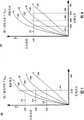
现在参照图7,I-V(即,电流-电压)曲线图200代表实例性无源元件存储器单元的电流电压关系。图中显示四个I-V曲线202、204、206、208,其分别对应于数据状态190、192、194、196且分别代表数据值10、00、01、11。如所述曲线图中所描绘,通过对照三个不同参考电流级Iref1(212)、Iref2(214)、Iref3(216)(其分别对应于电阻参考级Ref1、Ref2、Ref3,如上文参照图6所说明)比较在选定位线上产生的电流并使用所述选定位线上的单个读取电压210(VRD)来确定这四个状态。在此技术中,将所述位线上的电压设定为所述VRD电压,且将所述位线电流与一个、两个或三个参考电流级相比较。需要SBL上的VRD电压的仅一个稳定,但可通过适当选择三个参考电流级212、214、216来确定所有四个数据状态。此方法特别用于大约100nA或更大的存储器单元电流,在此情况下,所述Iref1电流的量值可以是约100nA。Referring now to FIG. 7, an I-V (ie, current-voltage)
现在参照图8,I-V曲线图220代表另一技术。如所述曲线图中所描绘,可针对三个不同的读取电压电平Vref1(228)、Vref2(226)、Vref3(224)(其分别对应于电阻参考级Ref1、Ref2、Ref3,如上文所说明)通过对照单个参考电流Iref1比较在选定位线上产生的电流并使用所述选定位线上的单个读取电流222来确定所述四个数据状态。在此技术中,将所述位线上的电压设定为等于三个参考电压224、226、228中的一者的读取电压VRD,且将所述位线电流与参考电流222相比较。需要所述选定位线上的VRD电压的仅一个稳定来确定LSB,但需要所述选定位线上的VRD电压的两个稳定来确定MSB。Referring now to FIG. 8, an
如果所述Vref1、Vref2及Vref3读取电压的值经操纵使得可使用单个位线参考电流(此允许针对此种偏置条件优化感测放大器电路)是特别有利的。此方法还特别用于具有相对低的电流(例如,针对最高电阻状态远远低于100nA)的存储器单元,因为通过将VRD电平变为2.5伏特或甚至更高来将所述高电阻状态的电流级设定为比针对图7中所示技术高的值。当使用较高的位线电流值时,可频繁地更容易地优化位线偏置电路及感测放大器电路。It is particularly advantageous if the values of the Vrefl, Vref2, and Vref3 read voltages are manipulated so that a single bit line reference current can be used (which allows the sense amplifier circuit to be optimized for such bias conditions). This method is also particularly useful for memory cells with relatively low currents (e.g., well below 100 nA for the highest resistance state), since the high resistance state is reduced by changing the VRD level to 2.5 volts or even higher. The current level is set to a higher value than for the technique shown in FIG. 7 . Bit line bias circuits and sense amplifier circuits can often be more easily optimized when higher bit line current values are used.
用于设定参考的另一优选方法并非完全通过Iref级。由于二极管电流变化,Icell随着单元的分布而指数地变化,因此三个Iref级将横跨宽广的范围。在所述整个宽广Iref范围中,所述感测放大器的灵敏性可能不像理想地那样。因此,图8所图解说明的此方法针对最低参考使用较高的Vref且针对最高参考使用较低的Vref。所有比较操作可使用相同的Iref值,因此Iref级不必在第一读取比较与第二读取比较之间改变以实现更快的读取速度及更小的电路复杂性。图9的电路适合于图8所图解说明的技术,其中仅需要一个电流比较电路308及309及OUTA。不需要OUTB电路。另外,在适当选择Vref电平的情况下,Iref可对于所有三个读取相同(其中尽可能理想地设计感测放大器的灵敏性)。由于需要最多两个读取循环且Iref不必在循环之间改变(如上文所说明),因此读取操作更快。Another preferred method for setting the reference is not to pass through the Iref level completely. Icell varies exponentially with the distribution of cells due to diode current variations, so the three Iref stages will span a wide range. The sensitivity of the sense amplifier may not be as ideal throughout the wide Iref range. Therefore, this method illustrated in Figure 8 uses a higher Vref for the lowest reference and a lower Vref for the highest reference. All compare operations can use the same Iref value, so the Iref level does not have to be changed between the first read compare and the second read compare to achieve faster read speed and less circuit complexity. The circuit of Figure 9 is suitable for the technique illustrated in Figure 8, where only one current comparison circuit 308 and 309 and OUTA are required. No OUTB circuit is required. Additionally, Iref can be the same for all three reads (where the sensitivity of the sense amplifier is designed as ideally as possible) with proper choice of Vref level. Read operations are faster since at most two read cycles are required and Iref does not have to change between cycles (as explained above).
可通过针对三个区分级变化Iref及Vref两者来组合图7与图8的方法以产生感测过程的最大误差容限。The methods of FIGS. 7 and 8 can be combined by grading both Iref and Vref for the three regions to yield the maximum error tolerance for the sensing process.
图9描绘用于读取多级存储器单元的实例性电路拓扑300连同到选定存储器单元101的字线及位线选择路径的表示图。此电路大致对应于图7中所说明的技术。字线选择路径322代表(举例来说)穿过字线驱动器电路(即,解码器“头”)且到达用于产生所述解码器头的经解码源选择总线的电路、到达在节点324上传送的接地电压的路径。位线选择路径318代表穿过位线驱动器电路且穿过到读取电路的任何总线耦合电路的路径。SELB数据总线316代表到此读取电路的输入。有用解码电路的额外细节说明于023-0048及023-0054申请案中、说明于023-0051及023-0056申请案中,且说明于023-0053及023-0058申请案中,下文提及所有所述申请案。FIG. 9 depicts a representation of an example circuit topology 300 for reading multi-level memory cells along with word line and bit line selection paths to a selected
通过在其栅极上接收二极管电压偏置信号315的箝位装置314来提供选定位线上的所需读取电压VRD。箝位装置314优选地是本机阈值NMOS装置。此偏置信号315可依据选定存储器单元沿位线的位置来变化,且经调整以在所述选定位线(即,节点106)上产生所需读取电压VRD。预充电晶体管304用于响应于现用-低预充电信号XBLP而对此拓扑中的各个节点(包括选定位线)进行预充电并对选择所述位线的路径进行解码。在将电压建立为所需值或所需值附近时,移除所述预充电信号,且电流镜装置306为所述选定位线提供电流负载。在电流镜栅极节点312上产生的电压耦合到将位线电流(用相同的量值或由所述电流镜缩放)反射到一对输出级的装置308、310,所述输出级中的每一者具有用于提供产生相应输出信号OUTA、OUTB的高压增益输出电路的相应电流源309、311。所述电路由在节点302上传送的共用分布式电压供电,所述电压稍微高于所需读取电压VRD。The desired read voltage VRD on the selected bit line is provided by a clamping device 314 which receives a diode voltage bias signal 315 on its gate. Clamping device 314 is preferably a native threshold NMOS device. This bias signal 315 can vary depending on the position of the selected memory cell along the bit line and is adjusted to produce the desired read voltage VRD on the selected bit line (ie, node 106). Precharge transistor 304 is used to precharge various nodes in this topology, including the selected bitline, and to decode the path that selects the bitline in response to active-low precharge signal XBLP. When the voltage is established at or near the desired value, the precharge signal is removed and the current mirror device 306 provides a current load for the selected bit line. The voltage developed on the current mirror gate node 312 is coupled to means 308, 310 that reflect the bit line current (in the same magnitude or scaled by the current mirror) to a pair of output stages, each of which One has a respective current source 309, 311 for providing a high voltage gain output circuit generating a respective output signal OUTA, OUTB. The circuit is powered by a common distributed voltage delivered on node 302, which is slightly higher than the required read voltage VRD.
此电路提供在选定位线上设定所需的读取电压,且进一步提供同时对照两个不同的参考电流比较所述选定位线电流以产生两个不同的输出信号。所述电路同时将Icell与多个Iref电流相比较,如包含装置308及电流参考309的第一电流比较器电路及包含装置310及电流参考311的第二电流比较器电路所示。OUTA及OUTB用于确定存储器状态,如上文参照图6更加详细的说明。可通过数据形成电路326来组合这些信号以产生MSB。所述选定位线上的此电压的单个稳定时间便足够。OUTA及OUTB输出中的单个一者可直接产生LSB(例如,使用不同的参考电流值),其中不需要其它输出。This circuit provides the read voltage required to set on a selected bit line, and further provides for simultaneous comparison of the selected bit line current against two different reference currents to generate two different output signals. The circuit compares Icell to multiple Iref currents simultaneously, as shown by a first current comparator circuit including device 308 and current reference 309 and a second current comparator circuit including device 310 and current reference 311 . OUTA and OUTB are used to determine memory status, as explained in more detail above with reference to FIG. 6 . These signals may be combined by data forming circuitry 326 to produce MSBs. A single settling time for this voltage on the selected bit line is sufficient. A single one of the OUTA and OUTB outputs can directly generate the LSB (eg, using a different reference current value), where no other output is required.
图10描绘用于写入多级存储器单元的实例性电路拓扑350。在此电路中,将选定位线的电压及电流两者控制为特定值。对于正向偏置(即,设定)操作,分布式供应节点在总线352上提供所需的电压偏置(VPP)。耦合到PMOS晶体管358的二极管电流偏置信号359在选定位线106上提供所需的电流限制。预充电装置356用于响应于XBLP预充电信号357而对选择路径进行预充电以增强性能。装置356、358两者耦合到节点360,节点360耦合到SELB总线316。模拟电路向所述位线供应反向偏置电压及电流以用于反向偏置(即,复位)编程。分布式供应节点在总线361上提供所需的电压偏置(-VRR)。耦合到NMOS晶体管362的二极管电流偏置信号363在选定位线上提供所需的电流限制。预充电装置364用于响应于BLP预充电信号365而对选择路径进行预充电。装置362、364两者耦合到节点366,节点366耦合到SELN总线367。FIG. 10 depicts an
可使用多个编程操作来对各种电阻状态进行编程,如上文参照图5所说明且如在下文提及的MA-163-1申请案中更加详细地说明。倾斜编程脉冲的使用说明于下文提及的SAND-01114US0及SAND-01114US1申请案中,且用于调整多个单元的电阻的技术说明于下文提及SAND-01117US0及SAND-01117US1申请案中。双位线源选择总线SELB及SELN更加详细地说明于下文提及的023-0051及023-0056申请案中。可在下文提及的第6,952,030号美国专利中找到对有用编程技术的额外了解。The various resistance states can be programmed using multiple programming operations, as explained above with reference to FIG. 5 and as explained in more detail in the MA-163-1 application referred to below. The use of ramped programming pulses is described in the SAND-01114US0 and SAND-01114US1 applications mentioned below, and techniques for adjusting the resistance of multiple cells are described in the SAND-01117US0 and SAND-01117US1 applications mentioned below. The dual bit line source select buses SELB and SELN are described in more detail in the 023-0051 and 023-0056 applications mentioned below. Additional insight into useful programming techniques can be found in US Patent No. 6,952,030 mentioned below.
实例性多级存储器单元包括具有金属氧化物(例如,过渡金属氧化物)及二极管的无源元件单元。其它合适的单元包括在二极管矩阵中具有电阻性材料的那些单元。实例包括可编程金属化连接、相变电阻器(例如,GST材料)、有机材料可变电阻器、复合金属氧化物、碳聚合物膜、经掺杂硫族化物玻璃及包含用以改变电阻的运动原子的肖特基(Schottky)势垒二极管。所选择的电阻性材料可提供一次性可编程(OTP)存储器单元或多写入存储器单元。另外,可采用具有由反向偏置力修改的导电性的多晶硅二极管。Exemplary multi-level memory cells include passive element cells having metal oxides (eg, transition metal oxides) and diodes. Other suitable cells include those with resistive material in the diode matrix. Examples include programmable metallization connections, phase change resistors (e.g., GST materials), organic material varistors, composite metal oxides, carbon polymer films, doped chalcogenide glasses, and Schottky barrier diodes for moving atoms. The resistive material selected can provide a one-time programmable (OTP) memory cell or a multiple-write memory cell. Additionally, polysilicon diodes with conductivity modified by reverse bias forces may be employed.
用于反向复位操作的有用存储器单元说明于颁发给S.布拉德·赫恩(S.BradHerner)等人的标题为“高密度三维存储器单元(High-Density Three-DimensionalMemory Cell)”的第6,952,030号美国专利中;且还说明于坦美·库玛(Tanmay Kumar)等人在2005年9月28日提出申请且在2007年4月26日出版为第2007-0090425号美国专利申请案出版物的标题为“用于使用包含具有可调整电阻的可切换半导体存储器元件的存储器单元的方法(Method for Using a Memory Cell Comprising SwitchableSemiconductor Memory Element with Trimmable Resistance)”的第11/237,167号美国申请案中。合适的金属氧化物存储器单元显示于S.布拉德·赫恩在2006年3月31日提出申请且标题为“包含电阻率切换氧化物或氮化物及反熔丝的多级非易失性存储器单元(Multilevel Nonvolatile Memory Cell Comprising a Resistivity-Switching Oxide orNitride and an Antifuse)”的第11/394,903号美国申请案中。使用相变材料的可提供多个电阻状态的适合存储器单元显示于罗伊E.施莱恩(Roy E.Scheuerlein)等人的标题为“包含电介质层及相变材料的串联非易失性存储器单元(Non-Volatile MemoryCell Comprising a Dielectric Layer and a Phase Change Material in Series)”的第2005-0158950号美国专利申请案出版物中。这些上文所提及揭示内容中的每一者以引用方式整体并入本文中。具有过渡-金属氧化物(例如,包括具有钴的那些氧化物)的其它实例性存储器单元及其中导引元件本身的多晶硅材料包含可切换电阻材料的实例性单元说明于下文提及的MA-163-1申请案中。Useful memory cells for reverse reset operations are described in Paper No. 1 entitled "High-Density Three-Dimensional Memory Cell" issued to S. Brad Herner et al. 6,952,030; and also described in Tanmay Kumar et al., filed September 28, 2005 and published April 26, 2007 as U.S. Patent Application No. 2007-0090425 in U.S. Application No. 11/237,167 entitled "Method for Using a Memory Cell Comprising Switchable Semiconductor Memory Element with Trimmable Resistance" . Suitable metal oxide memory cells are shown in the application filed March 31, 2006 by S. Brad Hearn and titled "Multilevel Non-Volatile Incorporating Resistivity-Switching Oxide or Nitride and Antifuse Memory unit (Multilevel Nonvolatile Memory Cell Comprising a Resistivity-Switching Oxide or Nitride and an Antifuse)" in US application No. 11/394,903. Suitable memory cells using phase-change materials that can provide multiple resistance states are shown in Roy E. Scheuerlein et al., entitled "Serial Non-Volatile Memory Cells Comprising Dielectric Layers and Phase-Change Materials." (Non-Volatile Memory Cell Comprising a Dielectric Layer and a Phase Change Material in Series)" in US Patent Application Publication No. 2005-0158950. Each of these above-mentioned disclosures is hereby incorporated by reference in its entirety. Other example memory cells with transition-metal oxides (including, for example, those with cobalt) and example cells in which the polysilicon material of the steering element itself comprises a switchable resistance material are described in MA-163 referenced below. -1 application pending.
另外,S.布拉德·赫恩等人在2005年5月9日提出申请且在2006年11月9日出版为第2006-0250836号美国专利申请案出版物的标题为“(Rewritable Memory CellComprising a Diode and a Resistance Switching Material)”的第11/125,939号美国申请案揭示并入有与氧化物(例如,氧化镍)串联的二极管的有用可重新写入存储器单元,其中可从低到高及从高到低电阻状态地反复切换所述存储器单元的电阻。S.布拉德·赫恩等人在2006年3月31日提出申请且在2006年11月9日出版为第2006-0250837号美国专利申请案出版物的标题为“包含二极管及电阻切换材料的非易失性存储器单元(Nonvolatile Memory Cell Comprising a Diode and a Resistance Switching Material)”的第11/395,995号美国申请案揭示使用正向偏置设定且使用反向偏置复位的OTP多级存储器单元。这些上文所提及揭示内容中的每一者以引用方式整体并入本文中。Additionally, S. Brad Hearn et al. filed on May 9, 2005 and published on November 9, 2006 as U.S. Patent Application Publication No. 2006-0250836 entitled "(Rewritable Memory Cell Comprising a Diode and a Resistance Switching Material), U.S. Application No. 11/125,939, discloses useful re-writable memory cells incorporating a diode in series with an oxide (e.g., nickel oxide), wherein switching from low to high and The resistance of the memory cell is toggled repeatedly from a high to a low resistance state. S. Brad Hearn et al. filed March 31, 2006 and published November 9, 2006 as U.S. Patent Application Publication No. 2006-0250837, entitled "Comprising Diode and Resistance Switching Materials U.S. Application No. 11/395,995 of "Nonvolatile Memory Cell Comprising a Diode and a Resistance Switching Material" discloses an OTP multi-level memory using forward bias setting and reverse bias reset unit. Each of these above-mentioned disclosures is hereby incorporated by reference in its entirety.
实例性多级存储器单元说明于上述第11/237,167号美国申请案中,且说明于下文提及的MA-163-1申请案中。Example multi-level memory cells are described in the aforementioned US Application No. 11/237,167, and in the MA-163-1 application referred to below.
以下文件说明可用于实践本发明的实例性无源元件存储器单元及相关非易失性存储器结构,其中每一者以引用方式整体并入本文中:The following documents describe example passive-element memory cells and related non-volatile memory structures that may be used to practice this disclosure, each of which is incorporated herein by reference in its entirety:
颁发给麦克G.约翰逊(Mark G.Johnson)等人的标题为“垂直堆叠的现场可编程非易失性存储器及制作方法(Vertically Stacked Field ProgrammableNonvolatile Memory and Method of Fabrication)”的第6,034,882号美国专利;U.S. Patent No. 6,034,882 entitled "Vertically Stacked Field Programmable Nonvolatile Memory and Method of Fabrication" issued to Mark G. Johnson et al. ;
颁发给N.约翰·奈尔(N.Johan Knall)等人的标题为“三维存储器阵列及制作方法(Three Dimensional Memory Array and Method of Fabrication)”的第6,420,215号美国专利;U.S. Patent No. 6,420,215, entitled "Three Dimensional Memory Array and Method of Fabrication," issued to N. Johan Knall et al.;
颁发给麦克·约翰逊(Mark Johnson)等人的标题为“垂直堆叠的现场可编程非易失性存储器及制作方法(Vertically-Stacked,Field Programmable,NonvolatileMemory and Method of Fabrication)”的第6,525,953号美国专利;U.S. Patent No. 6,525,953, entitled "Vertically-Stacked, Field Programmable, Nonvolatile Memory and Method of Fabrication," issued to Mark Johnson et al. ;
颁发给迈克尔·维沃达(Michael Vyvoda)等人的标题为“用于存储多位数字数据的数字存储器方法及系统(Digital Memory Method and System for StoringMultiple-Bit Digital Data)”的第6,490,218号美国专利;U.S. Patent No. 6,490,218, entitled "Digital Memory Method and System for Storing Multiple-Bit Digital Data," issued to Michael Vyvoda et al. ;
颁发给迈克尔·维沃达等人的标题为“有源装置中的电隔离柱(ElectricallyIsolated Pillars in Active Devices)”的第6,952,043号美国专利;及U.S. Patent No. 6,952,043, entitled "Electrically Isolated Pillars in Active Devices," issued to Michael Viwoda et al.; and
S.布拉德·赫恩等人的标题为“没有具有高及低阻抗状态的电介质反熔丝的非易失性存储器单元(Nonvolatile Memory Cell Without a Dielectric Antifuse HavingHigh-and Low-Impedance States)”的第US2005-0052915号美国专利申请案出版物。S. Brad Hearn et al. titled "Nonvolatile Memory Cell Without a Dielectric Antifuse Having High-and Low-Impedance States" US Patent Application Publication No. US2005-0052915.
以下申请案(每一者在2006年7月31日提出申请)说明可用于实践本发明的存储器单元结构、电路、系统及方法,其中每一者以引用方式整体并入本文中:The following applications, each filed July 31, 2006, describe memory cell structures, circuits, systems, and methods that may be used to practice the invention, each of which is incorporated herein by reference in its entirety:
罗伊·施莱恩及坦美·库玛的标题为“多用途存储器单元及存储器阵列(Multi-Use Memory Cell and Memory Array)”的第11/496,985号美国申请案(“10519-141”申请案);U.S. Application Serial No. 11/496,985, entitled "Multi-Use Memory Cell and Memory Array," to Roy Shlane and Tenmey Kumar (the "10519-141" application );
罗伊·施莱恩及坦美·库玛的标题为“用于使用多用途存储器单元及存储器阵列的方法(Method for Using a Multi-Use Memory Cell and Memory Array)”的第11/496,984号美国申请案(“10519-150”申请案);U.S. Application No. 11/496,984, entitled "Method for Using a Multi-Use Memory Cell and Memory Array," by Roy Shlane and Tenmey Kumar case (“10519-150” application);
罗伊·施莱恩的标题为“混合用途存储器阵列(Mixed-Use Memory Array)”的第11/496,874号美国申请案(“10519-142”申请案);U.S. Application No. 11/496,874 to Roy Schlain, entitled "Mixed-Use Memory Array" (the "10519-142" application);
罗伊·施莱恩的标题为“用于使用混合用途存储器阵列的方法(Method forUsing a Mixed-Use Memory Array)”的第11/496,983号美国申请案(“10519-151”申请案);U.S. Application No. 11/496,983 to Roy Schlain, entitled "Method for Using a Mixed-Use Memory Array" (the "10519-151" application);
罗伊·施莱恩及克里斯多佛·佩蒂(Christopher Petti)的标题为“具有不同数据状态的混合用途存储器阵列(Mixed-Use Memory Array With Different DataStates)”的第11/496,870号美国申请案(“10519-149”申请案);U.S. Application No. 11/496,870 to Roy Schlain and Christopher Petti, entitled "Mixed-Use Memory Array With Different DataStates" ("10519-149" application);
罗伊·施莱恩及克里斯多佛·佩蒂的标题为“用于使用具有不同的数据状态的混合用途存储器阵列的方法(Method for Using a Mixed-Use Memory Array WithDifferent Data States)”的第11/497,021号美国申请案(“10519-152”申请案);Roy Schlane and Christopher Petty, titled "Method for Using a Mixed-Use Memory Array With Different Data States" (Method for Using a Mixed-Use Memory Array With Different Data States) 11 /U.S. Application No. 497,021 (the "10519-152" application);
罗伊·施莱恩的标题为“非易失性存储器中的受控制脉冲操作(ControlledPulse Operations in Non-Volatile Memory)”的第11/461,393号美国申请案(“SAND-01114US0”申请案);U.S. Application No. 11/461,393 to Roy Schlain, entitled "Controlled Pulse Operations in Non-Volatile Memory" (the "SAND-01114US0" application);
罗伊·施莱恩的标题为“用于非易失性存储器中的受控制脉冲操作的系统(Systems for Controlled Pulse Operations in Non-Volatile Memory)”的第11/461,399号美国申请案(“SAND-01114US1”申请案);U.S. Application No. 11/461,399 to Roy Schlain, entitled "Systems for Controlled Pulse Operations in Non-Volatile Memory" ("SAND- 01114US1" application);
罗伊·施莱恩及克里斯多佛J.佩蒂的标题为“高带宽一次性现场可编程存储器(High Bandwidth One-Time Field-Programmable Memory)”的第11/461,410号美国申请案(“SAND-01115US0”申请案);U.S. Application No. 11/461,410, entitled "High Bandwidth One-Time Field-Programmable Memory," by Roy Schlain and Christopher J. Petty ("SAND -01115US0" application);
罗伊·施莱恩及克里斯多佛J.佩蒂的标题为“用于高带宽一次性现场可编程存储器的系统(Systems for High Bandwidth One-Time Field-Programmable Memory)”的第11/461,419号美国申请案(“SAND-01115US1”申请案);Ser. No. 11/461,419, Roy Schlain and Christopher J. Petty, entitled "Systems for High Bandwidth One-Time Field-Programmable Memory" US application (“SAND-01115US1” application);
罗伊·施莱恩及坦美·库玛的标题为“非易失性存储器中的反向偏置调整操作(Reverse Bias Trim Operations in Non-Volatile Memory)”的第11/461,424号美国申请案(“SAND-01117US0”申请案);U.S. Application No. 11/461,424, entitled "Reverse Bias Trim Operations in Non-Volatile Memory," by Roy Schlain and Tenmey Kumar ( "SAND-01117US0" application);
罗伊·施莱恩及坦美·库玛的标题为“用于非易失性存储器中的反向偏置调整操作的系统(Systems for Reverse Bias Trim Operations in Non-Volatile Memory)”的第11/461,431号美国申请案(“SAND-01117US1”申请案);Roy Schlein and Tenmei Kumar's paper titled "Systems for Reverse Bias Trim Operations in Non-Volatile Memory" No. 11/ U.S. Application No. 461,431 ("SAND-01117US1" application);
坦美·库玛、S.布拉德·赫恩、罗伊E.施莱恩及克里斯多佛J.佩蒂的标题为“用于使用包含具有可调整电阻的可切换半导体存储器元件的存储器单元的方法(Method for Using a Memory Cell Comprising Switchable Semiconductor MemoryElement with Trimmable Resistance)”的第11/496,986号美国申请案(“MA-163-1”申请案);Tanmy Kumar, S. Brad Hearn, Roy E. Schlein, and Christopher J. Petty titled "For the use of memory devices containing switchable semiconductor memory elements with adjustable resistance US Application No. 11/496,986 ("MA-163-1" application) for "Method for Using a Memory Cell Comprising Switchable Semiconductor MemoryElement with Trimmable Resistance";
卢卡G.法索里(Luca G.Fasoli)、克里斯多佛J.佩蒂及罗伊E.施莱恩的标题为“并入有可反转极性字线及位线解码器的无源元件存储器阵列(Passive ElementMemory Array Incorporating Reversible Polarity Word Line and Bit Line Decoders)”的第11/461,339号美国申请案(“023-0048”申请案);Luca G. Fasoli, Christopher J. Petty, and Roy E. Schlein are titled "Non-Surface Systems Incorporating Reversible Polarity Wordline and Bitline Decoders." U.S. Application No. 11/461,339 for Passive Element Memory Array Incorporating Reversible Polarity Word Line and Bit Line Decoders ("023-0048" application);
卢卡G.法索里、克里斯多佛J.佩蒂及罗伊E.施莱恩的标题为“用于使用并入有可反转极性字线及位线解码器的无源元件存储器阵列的方法(Method for Usinga Passive Element Memory Array Incorporating Reversible Polarity Word Line and BitLine Decoders)”的第11/461,364号美国申请案(“023-0054”申请案);Luca G. Fassoli, Christopher J. Petty, and Roy E. Schlein titled "Using Passive Component Memory Devices Incorporating Reversible Polarity Wordline and Bitline Decoders U.S. Application No. 11/461,364 (“023-0054” application) for “Method for Usinga Passive Element Memory Array Incorporating Reversible Polarity Word Line and BitLine Decoders”;
罗伊E.施莱恩、泰勒·索普(Tyler Thorp)及卢卡G.法索里的标题为“用于读取多级无源元件存储器单元阵列的设备(Apparatus for Reading a Multi-LevelPassive Element Memory Cell Array)”的第11/461,343号美国申请案(“023-0049”申请案);Roy E. Schlein, Tyler Thorp, and Luca G. Fassoli entitled "Apparatus for Reading a Multi-Level Passive Element Memory Cell Array (Apparatus for Reading a Multi-Level Passive Element Memory Cell Array)" U.S. Application No. 11/461,343 ("023-0049" application);
罗伊E.施莱恩、泰勒·索普及卢卡G.法索里的标题为“用于读取多级无源元件存储器单元阵列的方法(Method for Reading a Multi-Level Passive ElementMemory Cell Array)”的第11/461,367号美国申请案(“023-0055”申请案);Roy E. Schlein, Tyler Thorough, and Luca G. Fasoli titled "Method for Reading a Multi-Level Passive Element Memory Cell Array" U.S. Application No. 11/461,367 (“023-0055” application);
罗伊E.施莱恩及卢卡G.法索里的标题为“用于将读取/写入电路耦合到存储器阵列的双数据相依总线(Dual Data-Dependent Busses for Coupling Read/WriteCircuits to a Memory Array)”的第11/461,352号美国申请案(“023-0051”申请案);Roy E. Schlein and Luca G. Fassoli titled "Dual Data-Dependent Busses for Coupling Read/Write Circuits to a Memory Array" Array)” in U.S. Application No. 11/461,352 (“023-0051” application);
罗伊E.施莱恩及卢卡G.法索里的标题为“用于使用用于将读取/写入电路耦合到存储器阵列的双数据相依总线的方法(Method for Using Dual Data-DependentBusses for Coupling Read/Write Circuits to a Memory Array)”的第11/461,369号美国申请案(“023-0056”申请案);Roy E. Schlein and Luca G. Fassoli titled "Method for Using Dual Data-Dependent Busses for Using Dual Data-Dependent Busses for Coupling Read/Write Circuits to a Memory Array)" U.S. Application No. 11/461,369 ("023-0056" application);
罗伊E.施莱恩、卢卡G.法索里及克里斯多佛J.佩蒂的标题为“并入有用于存储器阵列块选择的两个数据总线的存储器阵列(Memory Array Incorporating TwoData Busses for Memory Array Block Selection)”的第11/461,359号美国申请案(“023-0052”申请案);Roy E. Schlein, Luca G. Fassoli, and Christopher J. Petty entitled "Memory Array Incorporating Two Data Busses for Memory Array Block Selection" Memory Array Block Selection)" U.S. Application No. 11/461,359 ("023-0052" application);
罗伊E.施莱恩、卢卡G.法索里及克里斯多佛J.佩蒂的标题为“用于使用用于存储器阵列块选择的两个数据总线的方法(Method for Using Two Data Busses forMemory Array Block Selection)”的第11/461,372号美国申请案(“023-0057”申请案);Roy E. Schlein, Luca G. Fassoli and Christopher J. Petty entitled "Method for Using Two Data Busses for Memory Array Block Selection for Memory Array Block Selection)" U.S. Application No. 11/461,372 ("023-0057" application);
罗伊E.施莱恩及卢卡G.法索里的标题为“用于块可选择存储器阵列的分级位线偏置总线(Hierarchical Bit Line Bias Bus for Block Selectable Memory Array)”的第11/461,362号美国申请案(“023-0053”申请案);及Roy E. Schlein and Luca G. Fassoli, Ser. No. 11/461,362 entitled "Hierarchical Bit Line Bias Bus for Block Selectable Memory Array" U.S. Application No. ("023-0053" application); and
罗伊E.施莱恩及卢卡G.法索里的标题为“用于使用用于块可选择存储器阵列的分级位线偏置总线的方法(Method for Using a Hierarchical Bit Line Bias Bus forBlock Selectable Memory Array)”的第11/461,376号美国申请案(“023-0058”申请案)。Roy E. Schlein and Luca G. Fassoli entitled "Method for Using a Hierarchical Bit Line Bias Bus for Block Selectable Memory Arrays" Array)” in U.S. Application No. 11/461,376 (“023-0058” application).
优选地,所述存储器阵列包括分段字线架构,且优选地是3D阵列。在某些实施例中,给定字线层上的字线与单个位线层上的位线相关联,而在某些实施例中,在所谓的“半镜像”布置中给定字线层上的字线在两个位线层之间共享(即,单个字线层与两个位线层界定两个存储器平面)。此种存储器阵列结构进一步说明于第6,879,505号美国专利中,其揭示内容以引用方式整体并入本文中。Preferably, the memory array comprises a segmented word line architecture, and is preferably a 3D array. In some embodiments, wordlines on a given wordline layer are associated with bitlines on a single bitline layer, while in some embodiments, a given wordline layer The wordlines above are shared between two bitline layers (ie, a single wordline layer and two bitline layers define two memory planes). Such a memory array structure is further described in US Patent No. 6,879,505, the disclosure of which is incorporated herein by reference in its entirety.
应了解,顶部、左侧、底部及右侧等称谓仅是用于存储器阵列的四个侧的方便描述性术语。可将块的字线分段实施为两个水平定向的交叉指状字线分段群组,且可将块的位线实施为两个垂直定向的交叉指状位线群组。每一相应的字线群组或位线群组可由位于阵列的四个侧中的一者上的相应解码器/驱动器电路及相应感测电路服务。It should be understood that the designations top, left, bottom and right are merely convenient descriptive terms used for the four sides of the memory array. The word line segments of a block can be implemented as two horizontally oriented groups of interdigitated word line segments, and the bit lines of a block can be implemented as two vertically oriented groups of interdigitated bit lines. Each respective group of wordlines or bitlines can be served by a respective decoder/driver circuit and a respective sense circuit located on one of the four sides of the array.
合适的列及行电路(包括所述解码的分级级、经解码总线的偏置电路组织及相关支持电路)说明于罗伊E.施莱恩及马修P.克罗利(Matthew P.Crowley)的标题为“利用具有双用途驱动器装置的存储器阵列线驱动器的多头式解码器结构(Multi-HeadedDecoder Structure Utilizing Memory Array Line Driver with Dual Purpose DriverDevice)”的第6,856,572号美国专利中;说明于罗伊E.施莱恩及马修P.克罗利的标题为“尤其适于具有极小布局间距的介接阵列线的树状解码器结构(Tree DecoderStructure Particularly Well-Suited to Interfacing Array Lines Having Extremely SmallLayout Pitch)”的第6,859,410号美国专利中;说明于肯尼斯K.索尔(Kenneth K.So)等人在2004年12月30日提出申请且在2006年7月6日出版为第2006-0145193号美国专利申请案出版物的第11/026,493号美国申请案“双模式解码器电路、并入有所述双模式解码器电路的集成电路存储器阵列及相关操作方法(Dual-Mode DecoderCircuit,Integrated Circuit Memory Array Incorporating Same,and Related Methods ofOperation)”中;且说明于卢卡G.法索里等人的“用于使用多头式解码器的多个级来对密集存储器阵列进行分级解码的设备及方法(Apparatus and Method for HierarchicalDecoding of Dense Memory Arrays Using Multiple Levels of Multiple-HeadedDecoders)”(第2006-0146639 A1号美国专利申请案出版物)中。这些所列举文件中每一者的揭示内容的全文以引用方式并入本文中。此外,额外有用的列及行选择电路说明于023-0048及023-0054申请案中,说明于023-0051及023-0056申请案中,说明于023-0052及023-0057申请案中,且说明于023-0053及023-0058申请案中,在本文中上文已提及所有所述申请案。Suitable column and row circuitry, including the hierarchical stages of decoding, the organization of the biasing circuits for the decoded bus, and associated support circuitry, are described in Roy E. Schlein and Matthew P. Crowley US Patent No. 6,856,572 entitled "Multi-Headed Decoder Structure Utilizing Memory Array Line Driver with Dual Purpose Driver Device"; described in Roy E. Schlein and Matthew P. Crowley titled "Tree Decoder Structure Particularly Well-Suited to Interfacing Array Lines Having Extremely Small Layout Pitch" US Patent No. 6,859,410 for "; described in Kenneth K. Soer (Kenneth K. So, et al., filed December 30, 2004 and published July 6, 2006 as US 2006-0145193 U.S. Application No. 11/026,493 of Patent Application Publication "Dual-Mode Decoder Circuit, Integrated Circuit Memory Array Incorporating Said Dual-Mode Decoder Circuit, Integrated Circuit Memory Array Incorporating Same, and Related Methods of Operation)"; and described in "Apparatus and Method for Hierarchical Decoding of Dense Memory Arrays Using Multiple Stages of a Multi-Head Decoder" by Luca G. Fasoli et al. and Method for Hierarchical Decoding of Dense Memory Arrays Using Multiple Levels of Multiple-Headed Decoders)" (US Patent Application Publication No. 2006-0146639 A1). The disclosures of each of these cited documents are incorporated herein by reference in their entirety. Additionally, additional useful column and row selection circuits are described in the 023-0048 and 023-0054 applications, in the 023-0051 and 023-0056 applications, in the 023-0052 and 023-0057 applications, and Illustrated in the 023-0053 and 023-0058 applications, all of which were referenced above in this text.
非镜像存储器阵列(例如,字线层仅与单个位线层相关联)说明于卢卡G.法索里等人在2005年3月31日提出申请且标题为“用于在存储器阵列中并入块冗余的方法及设备(Method and Apparatus for Incorporating Block Redundancy in a MemoryArray)”的第11/095,907号美国申请案(现在是第7,142,471号美国专利)中,其揭示内容的全文以引用方式并入本文中。Non-mirrored memory arrays (e.g., word line layers associated with only a single bit line layer) are described in Luca G. U.S. Application No. 11/095,907 (now U.S. Patent No. 7,142,471) for "Method and Apparatus for Incorporating Block Redundancy in a Memory Array," the disclosure of which is incorporated by reference in its entirety into this article.
如本文中所使用,行延伸跨越整个存储器格室(如果不是跨越整个带)且包括许多字线。如本文中所使用,“大致跨越多个阵列块”的总线或线包括跨越几乎所有阵列块,例如跨越除最后块(例如,给定总线不耦合到其的最后块)外的所有块。如本文中所使用,“将选定位线耦合到第一总线”分别意指将每一此种选定位线耦合到所述第一总线的对应总线线。如本文中所使用,字线(例如,包括字线分段)及位线通常代表正交阵列线,且大致遵循所属技术领域中的至少在读取操作期间驱动字线且感测位线的常见假设。此外,如本文中所使用,“全局线”(例如,全局选择线)是跨越一个以上存储器块的阵列线,但不应作出建议此种全局线必须横跨整个存储器阵列或大致跨越整个集成电路的特定推论。如本文中所使用,“相对于参考电流感测电流”意指确定所述“所感测”电流大于还是小于所述参考电流。As used herein, a row extends across an entire memory cell, if not across an entire stripe, and includes many word lines. As used herein, a bus or line that "spans substantially across a plurality of array blocks" includes spanning substantially all of the array blocks, eg, across all but the last block (eg, the last block to which a given bus is not coupled). As used herein, "coupling selected bitlines to a first bus" means coupling each such selected bitline to a corresponding bus line of the first bus, respectively. As used herein, wordlines (eg, including wordline segments) and bitlines generally represent orthogonal array lines and generally follow the art of driving wordlines and sensing bitlines at least during read operations. common assumptions. Also, as used herein, a "global line" (e.g., a global select line) is an array line that spans more than one memory block, but no suggestion should be made that such a global line necessarily spans the entire memory array or substantially the entire integrated circuit specific inferences. As used herein, "sensing a current relative to a reference current" means determining whether the "sensed" current is greater than or less than the reference current.
如本文中所使用,无源元件存储器阵列包括多个2端子存储器单元,其每一者连接在相关联的X线(例如,字线)与相关联的Y线(例如,位线)之间。此种存储器阵列可以是二维(平面)阵列或可以是具有一个以上存储器单元平面的三维阵列。每一此种存储器单元具有非线性导电率,其中反向方向上的电流(即,从阴极到阳极)低于正向方向上的电流。无源元件存储器阵列可以是一次性可编程(即,写入一次)存储器阵列或读取/写入(即,多写入)存储器阵列。As used herein, a passive element memory array includes a plurality of 2-terminal memory cells each connected between an associated X line (eg, word line) and an associated Y line (eg, bit line) . Such a memory array can be a two-dimensional (planar) array or can be a three-dimensional array with more than one plane of memory cells. Each such memory cell has a non-linear conductivity in which the current flow in the reverse direction (ie, from cathode to anode) is lower than the current flow in the forward direction. The passive element memory array may be a one-time programmable (ie, write once) memory array or a read/write (ie, write many times) memory array.
通常可将此类无源元件存储器单元视为具有在一个方向上引导电流的电流导引元件及能够改变其状态的另一组件(例如,熔丝、反熔丝、电容器、电阻性元件等)。可通过在存储器元件被选定时感测电流流动或电压降来读取所述存储器元件的编程状态。Such passive element memory cells can generally be thought of as having a current-steering element that directs current in one direction and another component (e.g., fuse, anti-fuse, capacitor, resistive element, etc.) capable of changing its state . The programmed state of a memory element can be read by sensing a current flow or a voltage drop when the memory element is selected.
各个图式中的各种阵列线的方向性仅是为了便于对阵列中的两个交叉线群组进行说明。如本文中所使用,集成电路存储器阵列是单片式集成电路结构,而不是封装在一起或紧密靠近的一个以上集成电路装置。The directionality of the various array lines in the various figures is for convenience only in describing the two groups of intersecting lines in the array. As used herein, an integrated circuit memory array is a monolithic integrated circuit structure rather than more than one integrated circuit device packaged together or in close proximity.
为清晰起见,并未显示及说明本文中所说明的实施方案的所有常规特征。在本文中,可使用连接块的单个节点的术语来说明框图。尽管如此,应了解,当上下文需要时,此种“节点”实际上可代表一对用于传送不同信号的节点,或可代表用于携载若干相关信号或用于携载形成数字字的多个信号或其它多位信号的多个单独导线(例如,总线)。In the interest of clarity, not all of the routine features of the implementations described herein are shown and described. In this document, block diagrams may be described in terms of individual nodes connecting blocks. Nevertheless, it should be understood that such a "node" may in fact represent a pair of nodes for carrying different signals, or may represent a pair of nodes for carrying several related signals or for carrying multiple nodes forming a digital word, as the context so requires. individual wires (for example, a bus) for individual signals or other multi-bit signals.
尽管通常假设为电路及物理结构,然而众所周知,在现代半导体设计及制作中,可将物理结构及电路体现为适于在后续设计、测试或制作阶段中以及在所形成的成品半导体集成电路中使用的计算机可读描述形式。相应地,针对传统电路或结构的权利要求可与其特定语言相一致地研究计算机可读编码及其表示法,无论所述编码及表示法是体现为媒体还是与合适的读取设施组合,以便允许对对应电路及/或结构进行制作、测试或设计改进。本发明预期包括所有在本文中说明及在所附权利要求书中界定的电路、相关方法或操作、用于制造此类电路的相关方法及此类电路及方法的计算机可读媒体编码。如本文中所使用,计算机可读媒体至少包括磁盘、磁带或其它磁性、光学、半导体(例如,快闪存储器卡、ROM)或电子媒体以及网络、有线、无线媒体或其它通信媒体。电路的编码可包括电路示意图信息、物理布局信息、动作仿真信息及/或可包括任何可据以代表或传递电路的其它编码。Although generally assumed to be electrical circuits and physical structures, it is well known that in modern semiconductor design and fabrication, physical structures and circuits can be embodied as suitable for use in subsequent design, test, or fabrication stages and in the resulting finished semiconductor integrated circuit A computer-readable description of . Accordingly, claims to conventional circuits or structures may, consistent with their specific language, address computer-readable code and representations thereof, whether embodied in media or combined with suitable reading facilities, in order to allow Make, test or design improvements to the corresponding circuits and/or structures. The present invention is intended to include all circuits described herein and defined in the appended claims, associated methods or operations, associated methods for making such circuits, and computer-readable medium encodings of such circuits and methods. As used herein, computer-readable media includes at least magnetic, magnetic tape or other magnetic, optical, semiconductor (eg, flash memory card, ROM) or electronic media, as well as network, wired, wireless or other communication media. The encoding of a circuit may include circuit schematic information, physical layout information, motion simulation information, and/or may include any other encoding by which a circuit can be represented or communicated.
以上详细说明仅说明了本发明许多种可能实施方案中的几种。因此,本详细说明打算作为说明性而非作为限制性。可在不背离本发明的范围及精神的情况下基于本文所述的说明对本文所揭示实施例做出变化及修改。打算仅由以上包括所有等效物的权利要求书来界定本发明的范围。此外,上文所说明的实施例是具体预期单独使用以及以各种组合形式使用。相应地,本文中未说明的其它实施例、变化形式及改进未必不包括在本发明的范围内。The foregoing detailed description illustrates only a few of the many possible embodiments of the invention. Accordingly, this detailed description is intended to be illustrative rather than restrictive. Variations and modifications of the embodiments disclosed herein can be made based on the description set forth herein without departing from the scope and spirit of the invention. It is intended that the scope of the present invention be defined only by the following claims including all equivalents. Furthermore, the embodiments described above are specifically intended to be used alone as well as in various combinations. Accordingly, other embodiments, variations, and improvements not described herein are not necessarily excluded from the scope of the present invention.
Claims (43)
Applications Claiming Priority (5)
| Application Number | Priority Date | Filing Date | Title |
|---|---|---|---|
| US11/461,343US7542337B2 (en) | 2006-07-31 | 2006-07-31 | Apparatus for reading a multi-level passive element memory cell array |
| US11/461,367 | 2006-07-31 | ||
| US11/461,367US7542338B2 (en) | 2006-07-31 | 2006-07-31 | Method for reading a multi-level passive element memory cell array |
| US11/461,343 | 2006-07-31 | ||
| PCT/US2007/074899WO2008016946A2 (en) | 2006-07-31 | 2007-07-31 | Method and apparatus for reading a multi-level passive element memory cell array |
Publications (2)
| Publication Number | Publication Date |
|---|---|
| CN101512663A CN101512663A (en) | 2009-08-19 |
| CN101512663Btrue CN101512663B (en) | 2013-08-28 |
Family
ID=38986076
Family Applications (1)
| Application Number | Title | Priority Date | Filing Date |
|---|---|---|---|
| CN2007800330616AActiveCN101512663B (en) | 2006-07-31 | 2007-07-31 | Method and apparatus for reading multi-level passive element memory cell array |
Country Status (2)
| Country | Link |
|---|---|
| US (1) | US7542337B2 (en) |
| CN (1) | CN101512663B (en) |
Families Citing this family (23)
| Publication number | Priority date | Publication date | Assignee | Title |
|---|---|---|---|---|
| US7492630B2 (en)* | 2006-07-31 | 2009-02-17 | Sandisk 3D Llc | Systems for reverse bias trim operations in non-volatile memory |
| US7522448B2 (en)* | 2006-07-31 | 2009-04-21 | Sandisk 3D Llc | Controlled pulse operations in non-volatile memory |
| US7542338B2 (en) | 2006-07-31 | 2009-06-02 | Sandisk 3D Llc | Method for reading a multi-level passive element memory cell array |
| US7499355B2 (en)* | 2006-07-31 | 2009-03-03 | Sandisk 3D Llc | High bandwidth one time field-programmable memory |
| US7499366B2 (en) | 2006-07-31 | 2009-03-03 | Sandisk 3D Llc | Method for using dual data-dependent busses for coupling read/write circuits to a memory array |
| US7719874B2 (en)* | 2006-07-31 | 2010-05-18 | Sandisk 3D Llc | Systems for controlled pulse operations in non-volatile memory |
| US8279704B2 (en) | 2006-07-31 | 2012-10-02 | Sandisk 3D Llc | Decoder circuitry providing forward and reverse modes of memory array operation and method for biasing same |
| US7499304B2 (en)* | 2006-07-31 | 2009-03-03 | Sandisk 3D Llc | Systems for high bandwidth one time field-programmable memory |
| US7495947B2 (en)* | 2006-07-31 | 2009-02-24 | Sandisk 3D Llc | Reverse bias trim operations in non-volatile memory |
| KR100909968B1 (en)* | 2007-06-12 | 2009-07-29 | 삼성전자주식회사 | Three-dimensional flash memory device with improved driving method and driving method |
| US7961494B2 (en) | 2008-04-11 | 2011-06-14 | Sandisk 3D Llc | Non-volatile multi-level re-writable memory cell incorporating a diode in series with multiple resistors and method for writing same |
| EP2182544A1 (en)* | 2008-10-31 | 2010-05-05 | FEI Company | Charged-particle optical system with dual specimen loading options |
| KR101635504B1 (en)* | 2009-06-19 | 2016-07-04 | 삼성전자주식회사 | Program method of non-volatile memory device with three-dimentional vertical channel structure |
| JP2011204302A (en)* | 2010-03-24 | 2011-10-13 | Toshiba Corp | Semiconductor memory device |
| US8482955B2 (en) | 2011-02-25 | 2013-07-09 | Micron Technology, Inc. | Resistive memory sensing methods and devices |
| WO2013015768A1 (en)* | 2011-07-22 | 2013-01-31 | Hewlett-Packard Development Company, L.P. | Circuit and method for reading a resistive switching device in an array |
| KR20130030616A (en)* | 2011-09-19 | 2013-03-27 | 에스케이하이닉스 주식회사 | Nonvolatile memory device |
| CN105103235B (en)* | 2013-01-31 | 2020-03-10 | 慧与发展有限责任合伙企业 | Non-volatile multi-level cell memory with decoupled bits for higher performance and energy efficiency |
| KR20140128482A (en)* | 2013-04-25 | 2014-11-06 | 에스케이하이닉스 주식회사 | Resistance Memory Device and Write Control Circuit, Memory Apparatus and Data Processing System Having the Same, and Operation Method Therefor |
| US9711190B2 (en)* | 2014-04-10 | 2017-07-18 | Taiwan Semiconductor Manufacturing Co. Limited | Stabilizing circuit |
| KR102292643B1 (en) | 2015-02-17 | 2021-08-23 | 삼성전자주식회사 | Resistive Memory Device, Resistive Memory System and Operating Method thereof |
| US10360973B2 (en)* | 2016-12-23 | 2019-07-23 | Western Digital Technologies, Inc. | Data mapping enabling fast read multi-level 3D NAND to improve lifetime capacity |
| KR102671481B1 (en)* | 2019-07-19 | 2024-06-03 | 삼성전자주식회사 | Memory device for avoiding multi-turn on of memory cell, and operating method thereof |
Citations (3)
| Publication number | Priority date | Publication date | Assignee | Title |
|---|---|---|---|---|
| US20030026120A1 (en)* | 2001-03-21 | 2003-02-06 | Scheuerlein Roy E. | Current sensing method and apparatus particularly useful for a memory array of cells having diode-like characteristics |
| US20050083747A1 (en)* | 2003-10-20 | 2005-04-21 | Taiwan Semicondutor Manufacturing Co. | Reference generator for multilevel nonlinear resistivity memory storage elements |
| US20050201148A1 (en)* | 2004-03-12 | 2005-09-15 | Super Talent Electronics, Inc. | Flash memory device and architecture with multi level cells |
Family Cites Families (60)
| Publication number | Priority date | Publication date | Assignee | Title |
|---|---|---|---|---|
| US2632058A (en)* | 1946-03-22 | 1953-03-17 | Bell Telephone Labor Inc | Pulse code communication |
| US3761896A (en)* | 1972-04-18 | 1973-09-25 | Ibm | Memory array of cells containing bistable switchable resistors |
| GB9122362D0 (en)* | 1991-10-22 | 1991-12-04 | British Telecomm | Resistive memory element |
| US5526306A (en)* | 1994-02-10 | 1996-06-11 | Mega Chips Corporation | Semiconductor memory device and method of fabricating the same |
| US5915167A (en)* | 1997-04-04 | 1999-06-22 | Elm Technology Corporation | Three dimensional structure memory |
| US6385074B1 (en)* | 1998-11-16 | 2002-05-07 | Matrix Semiconductor, Inc. | Integrated circuit structure including three-dimensional memory array |
| US6034882A (en)* | 1998-11-16 | 2000-03-07 | Matrix Semiconductor, Inc. | Vertically stacked field programmable nonvolatile memory and method of fabrication |
| US6072716A (en)* | 1999-04-14 | 2000-06-06 | Massachusetts Institute Of Technology | Memory structures and methods of making same |
| US6631085B2 (en)* | 2000-04-28 | 2003-10-07 | Matrix Semiconductor, Inc. | Three-dimensional memory array incorporating serial chain diode stack |
| US6420215B1 (en)* | 2000-04-28 | 2002-07-16 | Matrix Semiconductor, Inc. | Three-dimensional memory array and method of fabrication |
| US6856572B2 (en)* | 2000-04-28 | 2005-02-15 | Matrix Semiconductor, Inc. | Multi-headed decoder structure utilizing memory array line driver with dual purpose driver device |
| US6567287B2 (en)* | 2001-03-21 | 2003-05-20 | Matrix Semiconductor, Inc. | Memory device with row and column decoder circuits arranged in a checkerboard pattern under a plurality of memory arrays |
| US6618295B2 (en)* | 2001-03-21 | 2003-09-09 | Matrix Semiconductor, Inc. | Method and apparatus for biasing selected and unselected array lines when writing a memory array |
| US6545898B1 (en)* | 2001-03-21 | 2003-04-08 | Silicon Valley Bank | Method and apparatus for writing memory arrays using external source of high programming voltage |
| US6473332B1 (en)* | 2001-04-04 | 2002-10-29 | The University Of Houston System | Electrically variable multi-state resistance computing |
| US6525953B1 (en)* | 2001-08-13 | 2003-02-25 | Matrix Semiconductor, Inc. | Vertically-stacked, field-programmable, nonvolatile memory and method of fabrication |
| US6490218B1 (en)* | 2001-08-17 | 2002-12-03 | Matrix Semiconductor, Inc. | Digital memory method and system for storing multiple bit digital data |
| US6881623B2 (en)* | 2001-08-29 | 2005-04-19 | Micron Technology, Inc. | Method of forming chalcogenide comprising devices, method of forming a programmable memory cell of memory circuitry, and a chalcogenide comprising device |
| US20030047765A1 (en)* | 2001-08-30 | 2003-03-13 | Campbell Kristy A. | Stoichiometry for chalcogenide glasses useful for memory devices and method of formation |
| US6917069B2 (en)* | 2001-10-17 | 2005-07-12 | Silicon Storage Technology, Inc. | Semiconductor memory array of floating gate memory cells with buried bit-line and vertical word line transistor |
| JP2003208784A (en)* | 2002-01-10 | 2003-07-25 | Nec Corp | Nonvolatile magnetic storage device |
| AU2003233406A1 (en)* | 2002-03-15 | 2003-09-29 | Axon Technologies Corporation | Programmable structure, an array including the structure, and methods of forming the same |
| US6711068B2 (en)* | 2002-06-28 | 2004-03-23 | Motorola, Inc. | Balanced load memory and method of operation |
| US6850429B2 (en)* | 2002-08-02 | 2005-02-01 | Unity Semiconductor Corporation | Cross point memory array with memory plugs exhibiting a characteristic hysteresis |
| US6753561B1 (en)* | 2002-08-02 | 2004-06-22 | Unity Semiconductor Corporation | Cross point memory array using multiple thin films |
| US6831854B2 (en)* | 2002-08-02 | 2004-12-14 | Unity Semiconductor Corporation | Cross point memory array using distinct voltages |
| US6917539B2 (en)* | 2002-08-02 | 2005-07-12 | Unity Semiconductor Corporation | High-density NVRAM |
| US6965137B2 (en)* | 2002-08-02 | 2005-11-15 | Unity Semiconductor Corporation | Multi-layer conductive memory device |
| US7038935B2 (en)* | 2002-08-02 | 2006-05-02 | Unity Semiconductor Corporation | 2-terminal trapped charge memory device with voltage switchable multi-level resistance |
| US6906939B2 (en)* | 2002-08-02 | 2005-06-14 | Unity Semiconductor Corporation | Re-writable memory with multiple memory layers |
| US6856536B2 (en)* | 2002-08-02 | 2005-02-15 | Unity Semiconductor Corporation | Non-volatile memory with a single transistor and resistive memory element |
| US6859382B2 (en)* | 2002-08-02 | 2005-02-22 | Unity Semiconductor Corporation | Memory array of a non-volatile ram |
| US6834008B2 (en)* | 2002-08-02 | 2004-12-21 | Unity Semiconductor Corporation | Cross point memory array using multiple modes of operation |
| US6583003B1 (en)* | 2002-09-26 | 2003-06-24 | Sharp Laboratories Of America, Inc. | Method of fabricating 1T1R resistive memory array |
| US6801448B2 (en)* | 2002-11-26 | 2004-10-05 | Sharp Laboratories Of America, Inc. | Common bit/common source line high density 1T1R R-RAM array |
| US6859410B2 (en)* | 2002-11-27 | 2005-02-22 | Matrix Semiconductor, Inc. | Tree decoder structure particularly well-suited to interfacing array lines having extremely small layout pitch |
| WO2004061851A2 (en)* | 2002-12-19 | 2004-07-22 | Matrix Semiconductor, Inc | An improved method for making high-density nonvolatile memory |
| US7800933B2 (en) | 2005-09-28 | 2010-09-21 | Sandisk 3D Llc | Method for using a memory cell comprising switchable semiconductor memory element with trimmable resistance |
| US7800932B2 (en) | 2005-09-28 | 2010-09-21 | Sandisk 3D Llc | Memory cell comprising switchable semiconductor memory element with trimmable resistance |
| US7233024B2 (en)* | 2003-03-31 | 2007-06-19 | Sandisk 3D Llc | Three-dimensional memory device incorporating segmented bit line memory array |
| US6879505B2 (en)* | 2003-03-31 | 2005-04-12 | Matrix Semiconductor, Inc. | Word line arrangement having multi-layer word line segments for three-dimensional memory array |
| JP4192060B2 (en)* | 2003-09-12 | 2008-12-03 | シャープ株式会社 | Nonvolatile semiconductor memory device |
| JP4295680B2 (en)* | 2004-06-15 | 2009-07-15 | シャープ株式会社 | Semiconductor memory device |
| US7298665B2 (en)* | 2004-12-30 | 2007-11-20 | Sandisk 3D Llc | Dual-mode decoder circuit, integrated circuit memory array incorporating same, and related methods of operation |
| US7286439B2 (en)* | 2004-12-30 | 2007-10-23 | Sandisk 3D Llc | Apparatus and method for hierarchical decoding of dense memory arrays using multiple levels of multiple-headed decoders |
| US7142471B2 (en)* | 2005-03-31 | 2006-11-28 | Sandisk 3D Llc | Method and apparatus for incorporating block redundancy in a memory array |
| US7812404B2 (en)* | 2005-05-09 | 2010-10-12 | Sandisk 3D Llc | Nonvolatile memory cell comprising a diode and a resistance-switching material |
| US20060250836A1 (en)* | 2005-05-09 | 2006-11-09 | Matrix Semiconductor, Inc. | Rewriteable memory cell comprising a diode and a resistance-switching material |
| US20060273298A1 (en)* | 2005-06-02 | 2006-12-07 | Matrix Semiconductor, Inc. | Rewriteable memory cell comprising a transistor and resistance-switching material in series |
| US7345907B2 (en) | 2005-07-11 | 2008-03-18 | Sandisk 3D Llc | Apparatus and method for reading an array of nonvolatile memory cells including switchable resistor memory elements |
| US20070007579A1 (en)* | 2005-07-11 | 2007-01-11 | Matrix Semiconductor, Inc. | Memory cell comprising a thin film three-terminal switching device having a metal source and /or drain region |
| US7426128B2 (en)* | 2005-07-11 | 2008-09-16 | Sandisk 3D Llc | Switchable resistive memory with opposite polarity write pulses |
| US7362604B2 (en)* | 2005-07-11 | 2008-04-22 | Sandisk 3D Llc | Apparatus and method for programming an array of nonvolatile memory cells including switchable resistor memory elements |
| US7808810B2 (en) | 2006-03-31 | 2010-10-05 | Sandisk 3D Llc | Multilevel nonvolatile memory cell comprising a resistivity-switching oxide or nitride and an antifuse |
| US7495947B2 (en) | 2006-07-31 | 2009-02-24 | Sandisk 3D Llc | Reverse bias trim operations in non-volatile memory |
| US20080025069A1 (en) | 2006-07-31 | 2008-01-31 | Scheuerlein Roy E | Mixed-use memory array with different data states |
| US7499355B2 (en) | 2006-07-31 | 2009-03-03 | Sandisk 3D Llc | High bandwidth one time field-programmable memory |
| US7554832B2 (en) | 2006-07-31 | 2009-06-30 | Sandisk 3D Llc | Passive element memory array incorporating reversible polarity word line and bit line decoders |
| US7542338B2 (en) | 2006-07-31 | 2009-06-02 | Sandisk 3D Llc | Method for reading a multi-level passive element memory cell array |
| US20080023790A1 (en) | 2006-07-31 | 2008-01-31 | Scheuerlein Roy E | Mixed-use memory array |
- 2006
- 2006-07-31USUS11/461,343patent/US7542337B2/enactiveActive
- 2007
- 2007-07-31CNCN2007800330616Apatent/CN101512663B/enactiveActive
Patent Citations (3)
| Publication number | Priority date | Publication date | Assignee | Title |
|---|---|---|---|---|
| US20030026120A1 (en)* | 2001-03-21 | 2003-02-06 | Scheuerlein Roy E. | Current sensing method and apparatus particularly useful for a memory array of cells having diode-like characteristics |
| US20050083747A1 (en)* | 2003-10-20 | 2005-04-21 | Taiwan Semicondutor Manufacturing Co. | Reference generator for multilevel nonlinear resistivity memory storage elements |
| US20050201148A1 (en)* | 2004-03-12 | 2005-09-15 | Super Talent Electronics, Inc. | Flash memory device and architecture with multi level cells |
Also Published As
| Publication number | Publication date |
|---|---|
| CN101512663A (en) | 2009-08-19 |
| US7542337B2 (en) | 2009-06-02 |
| US20080025088A1 (en) | 2008-01-31 |
Similar Documents
| Publication | Publication Date | Title |
|---|---|---|
| CN101512663B (en) | Method and apparatus for reading multi-level passive element memory cell array | |
| US7542338B2 (en) | Method for reading a multi-level passive element memory cell array | |
| EP1965391B1 (en) | Non-volatile semiconductor memory device | |
| US7495984B2 (en) | Resistive memory devices including selected reference memory cells | |
| US8509025B2 (en) | Memory array circuit incorporating multiple array block selection and related method | |
| US7463546B2 (en) | Method for using a passive element memory array incorporating reversible polarity word line and bit line decoders | |
| US7486587B2 (en) | Dual data-dependent busses for coupling read/write circuits to a memory array | |
| US7554832B2 (en) | Passive element memory array incorporating reversible polarity word line and bit line decoders | |
| US7542370B2 (en) | Reversible polarity decoder circuit | |
| US8271856B2 (en) | Resistive memory devices and methods of controlling operations of the same | |
| JP2013539152A (en) | Decoder circuit for providing forward and reverse modes to the operation of a memory array, and method of biasing the same | |
| EP2052390B1 (en) | Method and apparatus for reading a multi-level passive element memory cell array | |
| US20080025093A1 (en) | Hierarchical bit line bias bus for block selectable memory array | |
| US20080025094A1 (en) | Method for using a hierarchical bit line bias bus for block selectable memory array | |
| US7525869B2 (en) | Method for using a reversible polarity decoder circuit | |
| EP2109863B1 (en) | Reversible polarity decoder circuit and related methods | |
| EP2062262B1 (en) | Method and apparatus for passive element memory array incorporating reversible polarity word line and bit line decoders | |
| EP2062263B1 (en) | Method and apparatus for dual data-dependent busses for coupling read/write circuits to a memory array |
Legal Events
| Date | Code | Title | Description |
|---|---|---|---|
| C06 | Publication | ||
| PB01 | Publication | ||
| C10 | Entry into substantive examination | ||
| SE01 | Entry into force of request for substantive examination | ||
| C14 | Grant of patent or utility model | ||
| GR01 | Patent grant | ||
| C41 | Transfer of patent application or patent right or utility model | ||
| C56 | Change in the name or address of the patentee | ||
| CP01 | Change in the name or title of a patent holder | Address after:Texas, USA Patentee after:SANDISK TECHNOLOGIES LLC Address before:Texas, USA Patentee before:Sandy Technology Corp. | |
| TR01 | Transfer of patent right | Effective date of registration:20160712 Address after:Texas, USA Patentee after:Sandy Technology Corp. Address before:California, USA Patentee before:Sandisk 3D LLC | |
| TR01 | Transfer of patent right | Effective date of registration:20250117 Address after:California, USA Patentee after:Shengdi Technology Co.,Ltd. Country or region after:U.S.A. Address before:American Texas Patentee before:SANDISK TECHNOLOGIES LLC Country or region before:U.S.A. | |
| TR01 | Transfer of patent right |