CN101506985A - Semiconductor device and semiconductor device manufacturing method - Google Patents
Semiconductor device and semiconductor device manufacturing methodDownload PDFInfo
- Publication number
- CN101506985A CN101506985ACNA2007800310951ACN200780031095ACN101506985ACN 101506985 ACN101506985 ACN 101506985ACN A2007800310951 ACNA2007800310951 ACN A2007800310951ACN 200780031095 ACN200780031095 ACN 200780031095ACN 101506985 ACN101506985 ACN 101506985A
- Authority
- CN
- China
- Prior art keywords
- film
- layer
- insulator
- semiconductor device
- gate electrode
- Prior art date
- Legal status (The legal status is an assumption and is not a legal conclusion. Google has not performed a legal analysis and makes no representation as to the accuracy of the status listed.)
- Pending
Links
Images


Landscapes
- Thin Film Transistor (AREA)
Abstract
Translated fromChinese
Description
Translated fromChinese技术领域technical field
本发明涉及半导体装置,特别是涉及薄膜晶体管(TFT)及其制造方法。The present invention relates to semiconductor devices, and more particularly, to thin film transistors (TFTs) and methods of manufacturing the same.
背景技术Background technique
一般地,液晶显示装置、有机EL装置、无机EL装置等显示装置是在具有一平坦主面的基板上把配线图形、电极图形等的导电图形顺次成膜并通过形成图形而形成。然后在构成电极膜、显示装置的元件上把必要的各种膜等顺次成膜,并通过形成图形来制作显示装置。Generally, display devices such as liquid crystal display devices, organic EL devices, and inorganic EL devices are formed by sequentially forming conductive patterns such as wiring patterns and electrode patterns on a substrate having a flat main surface and forming patterns. Then, various necessary films are sequentially formed on the electrode film and the elements constituting the display device, and the display device is produced by forming a pattern.
近年来,对于该种显示装置强烈要求大型化。为了形成大型的显示装置则需要在基板上高精度形成更多的显示元件,并把这些元件与配线图形电连接。这时,在基板上除了配线图形之外还形成绝缘膜、TFT(薄膜晶体管)元件、发光元件等以多层化的状态形成。其结果一般是在基板上得到台阶状的阶梯,配线图形越过这些阶梯来配线。In recent years, there has been a strong demand for upsizing of such display devices. In order to form a large display device, it is necessary to form more display elements with high precision on a substrate and electrically connect these elements to wiring patterns. At this time, in addition to the wiring pattern, an insulating film, TFT (Thin Film Transistor) elements, light emitting elements, and the like are formed in a multilayered state on the substrate. As a result, generally, stepped steps are obtained on the substrate, and the wiring pattern is wired over these steps.
进而,在显示装置被大型化时,配线图形自身就变长,因此需要降低该配线图形的电阻。消除配线图形的阶梯且把电阻变低的方法,例如被专利文献1、专利文献2和专利文献3所公开。专利文献1~3公开了:为了形成液晶显示器这样的平面显示器用配线,则在透明的基板表面形成配线并把与它是同等高度的透明绝缘材料与配线图形相接。在专利文献3中还公开了:利用加热冲压和CMP(Chemical Mechanical Polishing化学机械研磨)来使配线更平坦化的方法。Furthermore, when the size of the display device is increased, the wiring pattern itself becomes longer, so it is necessary to reduce the resistance of the wiring pattern. Methods of reducing the resistance by eliminating steps in the wiring pattern are disclosed in, for example, Patent Document 1, Patent Document 2, and Patent Document 3. Patent Documents 1 to 3 disclose that in order to form wiring for a flat-panel display such as a liquid crystal display, the wiring is formed on a transparent substrate surface and a transparent insulating material of the same height as the wiring pattern is brought into contact with the wiring pattern. Patent Document 3 also discloses a method of flattening wiring by hot stamping and CMP (Chemical Mechanical Polishing).
专利文献1:WO2004/110117号Patent Document 1: WO2004/110117
专利文献2:特愿2005-173050号公报Patent Document 2: Japanese Patent Application No. 2005-173050
专利文献3:特开2005-210081号公报Patent Document 3: JP-A-2005-210081
专利文献4:特开2002-296780号公报Patent Document 4: JP-A-2002-296780
专利文献5:特开2001-188343号公报Patent Document 5: JP-A-2001-188343
专利文献1中公开了:通过在由树脂图形形成的槽中埋设配线并且进行厚膜配线就能够提高显示装置的特性。且作为配线形成方法公开了喷墨法、网板印刷法等方法。Patent Document 1 discloses that the characteristics of a display device can be improved by embedding wiring in grooves formed of a resin pattern and performing thick-film wiring. In addition, methods such as an inkjet method and a screen printing method are disclosed as wiring forming methods.
但了解到所公开的方法在对基板的贴紧性上有问题。However, it is known that the disclosed method has a problem in adhesion to the substrate.
另一方面还了解到,当如专利文献1所记载的那样把配线由导电性油墨和网板印刷等形成时,配线的表面粗糙,且配线上形成的绝缘层等平坦性不好。当把由导电性油墨、网板印刷所形成的配线作为栅极电极使用时,由于配线表面粗糙而使通过通道的载流子传播率恶化,被观察到有成为高速动作障碍的现象。而且还了解到在导电性油墨、网板印刷等中若配线微细,则难于得到希望的形状。例如即使想用上述方法形成宽度20μm、长度50μm的栅极电极,电极材料也不能到达整个面,了解到在实用上不可能形成希望的图形。On the other hand, it is also known that when the wiring is formed by conductive ink, screen printing, etc. as described in Patent Document 1, the surface of the wiring is rough, and the flatness of the insulating layer formed on the wiring is not good. . When wiring formed by conductive ink or screen printing is used as a gate electrode, it has been observed that the carrier propagation rate through the channel is deteriorated due to the rough surface of the wiring, and it is observed that it becomes an obstacle to high-speed operation. Furthermore, it has been found that in conductive ink, screen printing, etc., if the wiring is fine, it is difficult to obtain a desired shape. For example, even if a gate electrode with a width of 20 μm and a length of 50 μm is formed by the above method, the electrode material cannot reach the entire surface, and it is found that it is practically impossible to form a desired pattern.
专利文献2为了解决这些问题,为了提高对基板的贴紧性,所提案的制造方法至少包括:在绝缘基板上进行表面修饰的工序、在该绝缘基板上形成树脂膜的工序、通过把该树脂膜形成图形而形成收容电极或配线的凹部的工序、向该凹部付与催化剂的工序、把该树脂膜加热固化的工序、利用镀层法在该凹部形成导电性材料的工序。栅极电极等的导电金属层例如由非电解镀层法形成Cu层,在其上利用有选择的CVD(Chemical VaporDeposition)法而形成W层作为Cu的扩散抑制层或是利用非电解镀层法而形成Ni层,这样来作为栅极电极。In order to solve these problems, in order to improve the adhesion to the substrate, the proposed manufacturing method at least includes: the process of surface modification on the insulating substrate, the process of forming a resin film on the insulating substrate, The process of patterning the film to form recesses for accommodating electrodes or wiring, applying a catalyst to the recesses, heating and curing the resin film, and forming a conductive material in the recesses by plating. The conductive metal layer such as the gate electrode is formed by, for example, a Cu layer by an electroless plating method, and a W layer is formed on it by a selective CVD (Chemical Vapor Deposition) method as a Cu diffusion suppression layer or by an electroless plating method. Ni layer, so as to serve as the gate electrode.
根据该方法,栅极电极对基板的贴紧性被改善,且即使是宽度20μm、长度50μm的栅极电极,也能够与尺寸大小无关地形成希望的图形。但了解到即使是该方法栅极电极的表面也粗糙、栅极电极上形成的栅极绝缘层平坦性也不好。例如由非电解镀层法形成的Cu层表面的平坦度为Ra是17.74nm、峰-谷值也达到193.92nm,其上形成的Ni层表面也成为平坦度为Ra是8.58nm、峰-谷值是68.7nm。由于这种表面粗糙,所以作为栅极绝缘膜而由CVD法形成的氮化硅表面即与半导体层的通道区域的界面也粗糙,了解到表面扩散的结果是载流子的移动度恶化。为了在栅极绝缘膜与通道区域的界面中维持平坦性而防止载流子的界面扩散,就需要使栅极电极的表面平坦度为Ra在1nm以下、峰-谷值在20nm以下。According to this method, the adhesion of the gate electrode to the substrate is improved, and even a gate electrode having a width of 20 μm and a length of 50 μm can be formed into a desired pattern regardless of its size. However, even with this method, the surface of the gate electrode is rough, and the flatness of the gate insulating layer formed on the gate electrode is not good. For example, the surface flatness of the Cu layer formed by the electroless plating method is Ra 17.74nm, and the peak-valley value reaches 193.92nm. It is 68.7nm. Due to this surface roughness, the surface of silicon nitride formed by CVD as a gate insulating film, that is, the interface with the channel region of the semiconductor layer is also rough, and it is known that mobility of carriers deteriorates as a result of surface diffusion. In order to maintain flatness at the interface between the gate insulating film and the channel region and prevent interfacial diffusion of carriers, the surface flatness of the gate electrode needs to be Ra of 1 nm or less and peak-to-valley value of 20 nm or less.
专利文献3中作为解决配线表面粗糙问题的方法提案是:利用冲压部件来按压绝缘膜和埋入配线的加热冲压处理或是CMP处理的工序。但近年来随着样品玻璃(マザ—ガラス)的基板尺寸大型化,特别是第五代1100mm×1300mm以上大小的玻璃基板中,这些使配线平坦化的方法变得不现实。加热冲压处理的微小玻璃变形会招致破损,且CMP的大型玻璃基板全面均匀研磨非常困难,带来成本的增大。Patent Document 3 proposes a hot stamping process or a CMP process in which an insulating film and embedded wiring are pressed using a stamping member as a method for solving the problem of rough wiring surfaces. However, as the substrate size of sample glass (maza-garas) has increased in recent years, especially in the fifth-generation glass substrates with a size of 1100 mm x 1300 mm or more, these methods of flattening the wiring have become unrealistic. Small glass deformation caused by heating and stamping will lead to breakage, and it is very difficult to uniformly polish a large glass substrate in CMP, resulting in an increase in cost.
且在镀层与周围树脂膜之间产生间隙的现象也被观测到。原因认为是镀层处理时的高温使树脂膨胀,而镀层形成后收缩的缘故。若存在这种间隙,则栅极绝缘膜出现电场集中而产生绝缘被破坏,栅极电极与通道区域短路。And the phenomenon that a gap is generated between the plating layer and the surrounding resin film was also observed. The reason is considered to be that the high temperature during the plating process expands the resin and shrinks after the plating is formed. If such a gap exists, electric field concentration occurs in the gate insulating film, and insulation breakdown occurs, and the gate electrode and the channel region are short-circuited.
发明内容Contents of the invention
本发明的目的在于提供一种栅极绝缘膜的平坦性优良的薄膜晶体管(TFT)及其制造方法。An object of the present invention is to provide a thin film transistor (TFT) having an excellent flatness of a gate insulating film and a method for manufacturing the same.
本发明的其他目的在于提供一种解决了栅极电极表面粗糙度和与周围绝缘层的间隙问题的半导体装置及其制造方法。Another object of the present invention is to provide a semiconductor device and a manufacturing method thereof that solve the problems of the surface roughness of the gate electrode and the gap with the surrounding insulating layer.
本发明的又其他目的在于提供一种具有界面平坦性优良的薄膜晶体管的显示装置及其制造方法。Yet another object of the present invention is to provide a display device having a thin film transistor with excellent interface flatness and a method for manufacturing the same.
以下记载本发明的形态。Embodiments of the present invention are described below.
(第一形态)(first form)
根据本发明第一形态的半导体装置则具有:基板、设置在该基板上且具有槽的绝缘体层、设置在该槽中并使其表面与所述绝缘体层的表面大致平坦的导电体层、设置在该导电体层上的绝缘膜、在该导电体层的至少一部分上方并且在该绝缘膜上设置的半导体层,其中,所述绝缘膜具有绝缘体涂布膜。The semiconductor device according to the first aspect of the present invention has: a substrate, an insulator layer provided on the substrate and having a groove, a conductor layer provided in the groove so that its surface is substantially flat with the surface of the insulator layer, An insulating film on the conductor layer, a semiconductor layer provided on at least a part of the conductor layer and on the insulating film, wherein the insulating film has an insulator coating film.
(第二形态)(second form)
在所述第一形态的半导体装置中,所述绝缘膜仅由所述绝缘体涂布膜构成。In the semiconductor device of the first aspect, the insulating film is composed only of the insulating coating film.
(第三形态)(third form)
在所述第一形态的半导体装置中,所述绝缘膜也可以具有其他的绝缘体膜。In the semiconductor device of the first aspect, the insulating film may include another insulating film.
(第四形态)(fourth form)
在所述第三形态的半导体装置中,所述其他的绝缘体膜优选是绝缘体CVD膜。In the semiconductor device of the third aspect, the other insulator film is preferably an insulator CVD film.
(第五形态)(fifth form)
在所述第三形态的半导体装置中,所述其他的绝缘体膜设置在所述绝缘体涂布膜与所述半导体层之间。In the semiconductor device of the third aspect, the other insulator film is provided between the insulator coating film and the semiconductor layer.
(第六形态)(sixth form)
在所述第三形态的半导体装置中,所述其他的绝缘体膜也可以设置在所述绝缘体涂布膜与所述导电体层之间。In the semiconductor device of the third aspect, the other insulator film may be provided between the insulator coating film and the conductor layer.
(第七形态)(seventh form)
在所述第一形态的半导体装置中,所述导电体层的一部分是栅极电极,该栅极电极上的所述绝缘膜是栅极绝缘膜,所述半导体层设置在所述栅极绝缘膜上。In the semiconductor device of the first aspect, a part of the conductor layer is a gate electrode, the insulating film on the gate electrode is a gate insulating film, and the semiconductor layer is provided on the gate insulating film. film.
(第八形态)(eighth form)
在所述第七形态的半导体装置中,源极电极和漏极电极的至少一个与所述半导体层电连接。In the semiconductor device of the seventh aspect, at least one of the source electrode and the drain electrode is electrically connected to the semiconductor layer.
(第九形态)(ninth form)
根据本发明第九形态的半导体装置,基板上的绝缘体层设置槽,在该槽中作为导电体层形成栅极电极以使其表面与所述绝缘体层的表面大致平坦,在该栅极电极上经由栅极绝缘膜而配置半导体层,源极电极和漏极电极的至少一个与该半导体层电连接,其中,具有把所述栅极绝缘膜设置在所述栅极电极上的绝缘体涂布膜和在其上形成的绝缘体CVD膜。According to the semiconductor device according to the ninth aspect of the present invention, the insulator layer on the substrate is provided with a groove, and the gate electrode is formed as a conductor layer in the groove so that the surface thereof is substantially flat with the surface of the insulator layer, and on the gate electrode A semiconductor layer is arranged via a gate insulating film, at least one of a source electrode and a drain electrode is electrically connected to the semiconductor layer, wherein there is an insulator coating film for disposing the gate insulating film on the gate electrode and an insulator CVD film formed thereon.
(第十形态)(tenth form)
在所述第七或第九形态的半导体装置中,所述绝缘体涂布膜其表面的平坦度为Ra是1nm以下,峰-谷值是20nm以下。In the semiconductor device according to the seventh or ninth aspect, the insulator coating film has a surface flatness Ra of 1 nm or less and a peak-to-valley value of 20 nm or less.
(第十一形态)(eleventh form)
在所述第七或第九形态的半导体装置中,所述栅极电极其表面的平坦度为Ra是3nm以上,峰-谷值是30nm以上。In the semiconductor device of the seventh or ninth aspect, the flatness of the surface of the gate electrode is Ra of 3 nm or more, and the peak-to-valley value is 30 nm or more.
(第十二形态)(twelfth form)
在所述第一或第九形态的半导体装置中,所述基板实质上是透明的绝缘体基板,所述绝缘体层实质上是透明的树脂层。In the semiconductor device of the first or ninth aspect, the substrate is a substantially transparent insulator substrate, and the insulator layer is a substantially transparent resin layer.
(第十三形态)(thirteenth form)
在所述第十二形态的半导体装置中,所述树脂层由含有碱可溶性脂环烯烃类树脂和感射线成分的感光性树脂组成物所形成。In the semiconductor device according to the twelfth aspect, the resin layer is formed of a photosensitive resin composition containing an alkali-soluble alicyclic olefin resin and a radiation-sensitive component.
(第十四形态)(fourteenth form)
在所述第十二形态的半导体装置中,所述树脂层具有从由丙烯类树脂、硅类树脂、氟类树脂、聚酰亚胺类树脂、聚烯烃类树脂、脂环式烯烃类树脂和环氧类树脂构成的群中选择的一种以上的树脂。In the semiconductor device according to the twelfth aspect, the resin layer is composed of acrylic resin, silicon resin, fluorine resin, polyimide resin, polyolefin resin, alicyclic olefin resin, and One or more resins selected from the group consisting of epoxy resins.
(第十五形态)(fifteenth form)
在所述第七或第九形态的半导体装置中,所述栅极电极至少具有基底贴紧层、导电金属层、导电金属扩散抑制层。In the semiconductor device of the seventh or ninth aspect, the gate electrode includes at least a base-adhering layer, a conductive metal layer, and a conductive metal diffusion suppressing layer.
(第十六形态)(sixteenth form)
在所述第一或第九形态的半导体装置中,所述绝缘体涂布膜把所述导电体层与所述绝缘体层之间的间隙填埋且在所述绝缘体层的表面上延伸。In the semiconductor device according to the first or ninth aspect, the insulator coating film fills the gap between the conductor layer and the insulator layer and extends over the surface of the insulator layer.
(第十七形态)(seventeenth form)
在所述第七或第九形态的半导体装置中,所述绝缘体涂布膜实质上是透明的,把所述栅极电极与所述绝缘体层之间的间隙填埋且在所述绝缘体层的表面上延伸。In the semiconductor device of the seventh or ninth aspect, the insulator coating film is substantially transparent, fills the gap between the gate electrode and the insulator layer, and extended on the surface.
(第十八形态)(Eighteenth Form)
在所述第四或第九形态的半导体装置中,所述绝缘体CVD膜实质上是透明的,并且在所述绝缘体层的表面上延伸的所述绝缘体涂布膜上延伸。In the semiconductor device of the fourth or ninth aspect, the insulator CVD film is substantially transparent and extends on the insulator coating film extending on the surface of the insulator layer.
(第十九形态)(Nineteenth Form)
在所述第一或第九形态的半导体装置中,所述绝缘体涂布膜是使含有金属有机化合物和金属无机化合物的至少一种化合物和溶剂的液体状涂布膜干燥、烧制而得到的膜。In the semiconductor device of the first or ninth aspect, the insulator coating film is obtained by drying and firing a liquid coating film containing at least one compound of a metal organic compound and a metal inorganic compound and a solvent. membrane.
(第二十形态)(twentieth form)
在所述第一或第九形态的半导体装置中,所述绝缘体层实质上是透明的树脂层,所述绝缘体涂布膜是使含有金属有机化合物和金属无机化合物的至少一个和溶剂的液体状涂布膜干燥并在300℃以下烧制而得到的膜。In the semiconductor device of the first or ninth aspect, the insulator layer is a substantially transparent resin layer, and the insulator coating film is a liquid containing at least one of a metal organic compound and a metal inorganic compound and a solvent. A film obtained by drying the coated film and firing it at 300°C or less.
(第二十一形态)(21st Form)
在所述第一或第九形态的半导体装置中,所述绝缘体涂布膜的介电常数优选2.6以上。In the semiconductor device of the first or ninth aspect, the dielectric constant of the insulator coating film is preferably 2.6 or more.
(第二十二形态)(twenty-second form)
在所述第四或第九形态的半导体装置中,所述绝缘体CVD膜的介电常数优选4以上。In the semiconductor device of the fourth or ninth aspect, the dielectric constant of the insulator CVD film is preferably 4 or more.
(第二十三形态)(twenty-third form)
在所述第七或第九形态的半导体装置中,所述栅极绝缘膜的厚度按EOT(二氧化硅换算)优选是95nm到200nm。In the semiconductor device of the seventh or ninth aspect, the thickness of the gate insulating film is preferably 95 nm to 200 nm in terms of EOT (equivalent to silicon dioxide).
(第二十四形态)(twenty-fourth form)
在所述第四或第九形态的半导体装置中,所述绝缘体CVD膜的厚度按EOT(二氧化硅换算)优选是80nm到185nm。In the semiconductor device of the fourth or ninth aspect, the thickness of the insulator CVD film is preferably 80 nm to 185 nm in terms of EOT (equivalent to silicon dioxide).
(第二十五形态)(twenty-fifth form)
在所述第一或第九形态的半导体装置中,所述绝缘体涂布膜的厚度按EOT(二氧化硅换算)优选是15nm到120nm。In the semiconductor device of the first or ninth aspect, the thickness of the insulator coating film is preferably 15 nm to 120 nm in terms of EOT (equivalent to silicon dioxide).
(第二十六形态)(twenty-sixth form)
在所述第十五形态的半导体装置中,所述导电金属层具有Cu、Ag的至少一个,所述导电金属扩散抑制层具有从Ni、W、Ta、Nb、Ti的任一个选择的金属。In the semiconductor device according to the fifteenth aspect, the conductive metal layer has at least one of Cu and Ag, and the conductive metal diffusion suppressing layer has a metal selected from any one of Ni, W, Ta, Nb, and Ti.
(第二十七形态)(twenty-seventh form)
根据本发明,能够得到使用所述第一或第九形态的半导体装置制造的显示装置。According to the present invention, a display device manufactured using the semiconductor device of the first or ninth aspect can be obtained.
(第二十八形态)(twenty-eighth form)
在所述第二十七形态的显示装置中,所述显示装置是液晶显示装置或是有机EL显示装置。In the display device of the twenty-seventh aspect, the display device is a liquid crystal display device or an organic EL display device.
(第二十九形态)(twenty-ninth form)
根据本发明第二十九形态的半导体装置的制造方法,其中,包括:在基板上设置具有槽的绝缘体层的工序、在该槽中形成导电体层以使其表面与所述绝缘体层的表面大致平坦的工序、在该导电体层上形成绝缘体涂布膜的工序、在所述绝缘体涂布膜的至少一部分上形成半导体层的工序。A method of manufacturing a semiconductor device according to the twenty-ninth aspect of the present invention, including the steps of providing an insulator layer having a groove on a substrate, and forming a conductor layer in the groove such that the surface thereof is aligned with the surface of the insulator layer. a substantially flat step, a step of forming an insulator coating film on the conductor layer, and a step of forming a semiconductor layer on at least a part of the insulator coating film.
(第三十形态)(Thirtieth Form)
在所述第二十九形态的制造方法中,在形成所述绝缘体涂布膜的工序之前或之后也可以具有形成其他绝缘体膜的工序。In the production method of the twenty-ninth aspect, a step of forming another insulating film may be included before or after the step of forming the insulating coating film.
(第三十一形态)(Thirty-first form)
在所述第二十九形态的制造方法中,优选通过CVD来形成所述其他的绝缘体膜。In the manufacturing method of the twenty-ninth aspect, it is preferable to form the other insulating film by CVD.
(第三十二形态)(Thirty-second form)
在所述第二十九形态的制造方法中,也可以把所述导电体层的一部分作为栅极电极,把该栅极电极上的所述绝缘体涂布膜作为栅极绝缘膜的至少一部分,把所述半导体层设置在所述栅极绝缘膜上。In the manufacturing method of the twenty-ninth aspect, a part of the conductive layer may be used as a gate electrode, and the insulator coating film on the gate electrode may be used as at least a part of the gate insulating film, The semiconductor layer is provided on the gate insulating film.
(第三十三形态)(Thirty-third form)
在所述第二十九形态的制造方法中,还具有所述半导体层形成源极电极和漏极电极的至少一个的工序。In the manufacturing method of the twenty-ninth aspect, there is further a step of forming at least one of a source electrode and a drain electrode on the semiconductor layer.
(第三十四形态)(Thirty-fourth Form)
在本发明第三十四形态的半导体装置的制造方法中,其中,包括:在基板上设置具有槽的绝缘体层的工序、在该槽中形成栅极电极以使其表面与所述绝缘体层的表面大致平坦的工序、在该栅极电极上形成绝缘体涂布膜的工序、利用CVD在所述绝缘体涂布膜上形成电介质膜的工序、在所述电介质膜上形成半导体层的工序、把源极电极和漏极电极的至少一个与该半导体层电连接的工序。A method for manufacturing a semiconductor device according to a thirty-fourth aspect of the present invention, including the steps of providing an insulator layer having a groove on the substrate, forming a gate electrode in the groove such that its surface is in contact with the insulator layer. The process of forming a substantially flat surface, the process of forming an insulator coating film on the gate electrode, the process of forming a dielectric film on the insulator coating film by CVD, the process of forming a semiconductor layer on the dielectric film, and the source A step of electrically connecting at least one of the electrode electrode and the drain electrode to the semiconductor layer.
(第三十五形态)(Thirty-fifth Form)
在本发明第三十二或第三十四形态的制造方法中,形成所述绝缘体涂布膜的工序具有:把含有金属有机化合物和金属无机化合物的至少一种化合物和溶剂的液体状材料向所述栅极电极上涂布的工序、使涂布的膜干燥的工序、把干燥的膜进行烧制的工序。In the production method according to the thirty-second or thirty-fourth aspect of the present invention, the step of forming the insulator coating film includes: feeding a liquid material containing at least one compound of a metal-organic compound and a metal-inorganic compound and a solvent to the The step of coating on the gate electrode, the step of drying the coated film, and the step of firing the dried film.
(第三十六形态)(Thirty-sixth Form)
在本发明第三十二或第三十四形态的制造方法中,形成所述栅极电极的工序具有利用镀层法、印刷法、喷墨法或喷溅法来形成导电金属层的工序。In the manufacturing method according to the thirty-second or thirty-fourth aspect of the present invention, the step of forming the gate electrode includes a step of forming a conductive metal layer by a plating method, a printing method, an inkjet method, or a sputtering method.
(第三十七形态)(Thirty-seventh form)
在本发明第三十五形态的制造方法中,形成所述绝缘体涂布膜的工序具有使所述液体状材料把所述栅极电极与所述绝缘体层之间的间隙填埋,且在所述绝缘体层的表面上延伸涂布的工序。In the manufacturing method according to the thirty-fifth aspect of the present invention, the step of forming the insulator coating film includes filling the gap between the gate electrode and the insulator layer with the liquid material, and The step of stretch coating on the surface of the above-mentioned insulator layer.
(第三十八形态)(Thirty-eighth form)
在本发明第二十九或第三十四形态的制造方法中,在所述基板上设置具有槽的绝缘体层的工序具有:在所述基板上形成树脂膜的工序、通过把该树脂膜形成图形而形成用于收容所述栅极电极的槽的工序。In the production method according to the twenty-ninth or thirty-fourth aspect of the present invention, the step of providing the insulator layer having grooves on the substrate includes a step of forming a resin film on the substrate, forming the resin film and forming a groove for accommodating the gate electrode by patterning.
(第三十九形态)(Thirty-ninth form)
在本发明第三十五形态的制造方法中,把所述烧制在惰性气体环境中或大气环境进行。In the production method according to the thirty-fifth aspect of the present invention, the firing is performed in an inert gas atmosphere or an air atmosphere.
(第四十形态)(fortieth form)
根据本发明还能够得到液晶显示装置或有机EL显示装置的制造方法,其具有使用本发明第二十九或第三十四形态的制造方法来形成半导体装置的工序。According to the present invention, there can also be obtained a method of manufacturing a liquid crystal display device or an organic EL display device, which has a step of forming a semiconductor device using the manufacturing method of the twenty-ninth or thirty-fourth aspect of the present invention.
根据本发明,通过在表面粗糙的栅极电极上设置绝缘体涂布膜而能够使其表面的平坦度为Ra是1nm以下、峰-谷值是20nm以下。其结果是能够把栅极绝缘膜的表面平坦化,与通道区域的界面变平坦而防止载流子的界面扩散,达到高的载流子移动度。且把栅极电极与其周围绝缘层之间的间隙填埋,提供从栅极电极上达到绝缘层表面上的平坦表面,能够防止栅极绝缘膜的被破坏。According to the present invention, by providing an insulator coating film on a rough-surfaced gate electrode, it is possible to make the surface flatness Ra 1 nm or less and peak-valley value 20 nm or less. As a result, the surface of the gate insulating film can be flattened, and the interface with the channel region can be flattened to prevent interfacial diffusion of carriers and achieve a high degree of carrier mobility. Furthermore, filling the gap between the gate electrode and its surrounding insulating layer provides a flat surface reaching from the gate electrode to the surface of the insulating layer, which can prevent the gate insulating film from being damaged.
附图说明Description of drawings
图1是表示本发明第一实施例薄膜晶体管结构一例的剖面图;1 is a cross-sectional view showing an example of the structure of a thin film transistor according to the first embodiment of the present invention;
图2是把图1所示薄膜晶体管的栅极电极部结构一例放大表示的剖面图;2 is an enlarged cross-sectional view showing an example of the gate electrode structure of the thin film transistor shown in FIG. 1;
图3是用于把图1所示的薄膜晶体管制造方法一例按工序顺序说明的剖面图;3 is a cross-sectional view for explaining an example of the manufacturing method of the thin film transistor shown in FIG. 1 in order of steps;
图4是用于把图1所示的薄膜晶体管制造方法一例按工序顺序说明的剖面图;4 is a cross-sectional view for explaining an example of the manufacturing method of the thin film transistor shown in FIG. 1 in order of steps;
图5是用于把图1所示的薄膜晶体管制造方法一例按工序顺序说明的剖面图;5 is a cross-sectional view for explaining an example of the manufacturing method of the thin film transistor shown in FIG. 1 in order of steps;
图6是用于把图1所示的薄膜晶体管制造方法一例按工序顺序说明的剖面图;6 is a cross-sectional view for explaining an example of the manufacturing method of the thin film transistor shown in FIG. 1 in order of steps;
图7是用于把图1所示的薄膜晶体管制造方法一例按工序顺序说明的剖面图;7 is a cross-sectional view for explaining an example of the manufacturing method of the thin film transistor shown in FIG. 1 in order of steps;
图8是表示本发明第一实施例薄膜晶体管中外涂层膜FIB剖面的照片的图;FIG. 8 is a diagram showing a photo of the cross-section of the outer coating film FIB in the thin film transistor of the first embodiment of the present invention;
图9是表示本发明第二实施例薄膜晶体管结构一例的剖面图;9 is a cross-sectional view showing an example of the structure of a thin film transistor according to the second embodiment of the present invention;
图10是把图9所示薄膜晶体管的栅极电极部结构一例放大表示的剖面图;10 is an enlarged cross-sectional view showing an example of the gate electrode structure of the thin film transistor shown in FIG. 9;
图11是用于把图9所示的薄膜晶体管制造方法一例按工序顺序说明的剖面图;11 is a cross-sectional view for explaining an example of the thin film transistor manufacturing method shown in FIG. 9 in order of steps;
图12是用于把图9所示的薄膜晶体管制造方法一例按工序顺序说明的剖面图;12 is a cross-sectional view for explaining an example of the manufacturing method of the thin film transistor shown in FIG. 9 in order of steps;
图13是用于把图9所示的薄膜晶体管制造方法一例按工序顺序说明的剖面图;13 is a cross-sectional view for explaining an example of the manufacturing method of the thin film transistor shown in FIG. 9 in order of steps;
图14是用于把图9所示的薄膜晶体管制造方法一例按工序顺序说明的剖面图;14 is a cross-sectional view for explaining an example of the thin film transistor manufacturing method shown in FIG. 9 in order of steps;
图15是用于把图9所示的薄膜晶体管制造方法一例按工序顺序说明的剖面图;15 is a cross-sectional view for explaining an example of the manufacturing method of the thin film transistor shown in FIG. 9 in order of steps;
图16是表示本发明第三实施例薄膜晶体管结构一例的剖面图;16 is a cross-sectional view showing an example of the structure of a thin film transistor according to the third embodiment of the present invention;
图17是表示本发明第二实施例薄膜晶体管中外涂层膜FIB剖面的照片的图。Fig. 17 is a diagram showing a photograph of a cross-section of an overcoat film FIB in a thin film transistor according to the second embodiment of the present invention.
具体实施方式Detailed ways
使用图来说明本发明的第一实施例。A first embodiment of the present invention will be described using the drawings.
[第一实施例][first embodiment]
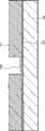
图1适用液晶显示装置,是表示本发明薄膜晶体管(TFT:Thin FilmTransistor)结构一例的剖面图。参照图1,薄膜晶体管具有:在玻璃基板(绝缘基板)10上形成的由透明感光性树脂构成的透明树脂膜(绝缘体层)11、透明树脂膜11形成的达到玻璃基板10且形成到与透明树脂膜11大致同一高度的栅极电极(导电体层)12。薄膜晶体管还具有:在整个透明树脂膜11和栅极电极12上形成的由绝缘体涂布膜(外涂层膜)131和在其上的CVD电介质膜(绝缘体CVD膜)132构成的栅极绝缘膜13、经由栅极绝缘膜13在栅极电极12上形成的半导体层14、与半导体层14连接的源极电极15和漏极电极16。1 is a cross-sectional view showing an example of the structure of a thin film transistor (TFT: Thin Film Transistor) of the present invention, which is applied to a liquid crystal display device. Referring to FIG. 1 , the thin film transistor has: a transparent resin film (insulator layer) 11 formed of a transparent photosensitive resin formed on a glass substrate (insulating substrate) 10; The
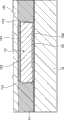
图2是把第一实施例薄膜晶体管的栅极电极部结构放大表示的剖面图。图示的栅极电极12被埋设在平坦的透明树脂膜11所形成的槽中,从玻璃基板10侧开始到半导体层侧(即从图的下方开始顺序)包括有:基底贴紧层121、催化剂层122、导电金属层123和导电金属扩散抑制层124。如图所示,使栅极电极12的表面与透明树脂膜11的表面被形成大致是同一平面地埋设在透明树脂膜11的槽中。因此,栅极电极12上部结构的平坦性被确保,但微观看时则平坦性有问题。即,以前非电解镀层的导电金属层123(Cu层)表面的平坦度为Ra是17.74nm、峰-谷(P-V)值也达到193.92nm,在其上形成的导电金属扩散抑制层124(非电解镀层Ni层)的表面平坦度也为Ra是8.58nm、峰-谷值是68.7nm。Fig. 2 is an enlarged cross-sectional view showing the structure of the gate electrode portion of the thin film transistor of the first embodiment. The
本发明在栅极电极12和透明树脂膜11上形成厚度40nm的绝缘体涂布膜131。该绝缘体涂布膜131把栅极电极12与透明树脂膜11之间的间隙112填埋,且提供不反映栅极电极12表面凹凸的Ra是0.24nm、峰-谷值是2.16nm的平坦表面。即使栅极电极表面的平坦度为Ra是3nm以上、峰-谷值是30nm以上,这些值也充分满足绝缘体涂布膜所要求的Ra是1nm以下、峰-谷值是20nm以下的值。In the present invention, an
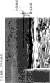
图8是把镀层配线的在栅极电极上形成绝缘体涂布膜(外涂层膜)的结构利用FIB加工,并表示观察剖面状况的电子显微镜照片。如图8所示,了解到形成不依赖于基底粗糙度的平坦表面。FIG. 8 is an electron micrograph of a structure in which an insulator coating film (overcoat film) is formed on a gate electrode of plated wiring by FIB processing, and shows the state of cross-section observation. As shown in FIG. 8 , it was learned that a flat surface was formed independent of the roughness of the substrate.
其结果是,利用CVD法在绝缘体涂布膜(外涂层膜)131上形成的厚度150~160nm的氮化硅电介质膜(CVD电介质膜)132的表面能够得到Ra是0.70nm、峰-谷值是7.54nm的平坦性(图2)。该结果由于能够使在栅极绝缘膜13上形成的半导体层不产生由栅极电极引起的凹凸地形成薄膜晶体管(TFT),所以能够大幅度提高载流子的移动度。As a result, the surface of the silicon nitride dielectric film (CVD dielectric film) 132 with a thickness of 150 to 160 nm formed on the insulator coating film (overcoat film) 131 by the CVD method can obtain Ra of 0.70 nm, peak-valley The value is a flatness of 7.54 nm (FIG. 2). As a result, since a thin film transistor (TFT) can be formed without causing unevenness due to the gate electrode in the semiconductor layer formed on the
作为绝缘体涂布膜(外涂层膜)131能够使用SOG(旋涂式玻璃法スピンオンガラス)。SOG膜能够根据成为膜的硅氧烷成分和作为溶剂的酒精成分等来调整。把该溶液利用旋转涂布法向基板上涂布,通过热处理使溶液等蒸发,当膜固化就形成SOG绝缘膜。所说的SOG是这些溶剂和形成的膜的总称。SOG按照硅氧烷的结构被分类为:石英玻璃、烷基硅氧烷聚合物、烷基倍半硅氧烷聚合物(MSQ)、氢化倍半硅氧烷聚合物(HSQ)、氢化烷基倍半硅氧烷聚合物(HOSQ)。若按照涂布材料分类,则硅玻璃是第一代无机SOG,烷基硅氧烷聚合物是第一代有机SOG,HSQ是第二代无机SOG,MSQ和HOSQ是第二代有机SOG。关于涂布膜的说明是,这些多在500℃以上进行烧制,在使用任何透明树脂层时由于不能设定成高温,所以使用烧制温度是300℃以下的。代替以上这样的Si有机化合物、Si无机化合物,也能够使用把其他有机金属化合物、金属无机化合物的至少一个溶解为有机溶剂的(特别是烧制温度是300℃以下的)。作为其他金属能够例举Ti、Ta、Al、Sn、Zr等。SOG (Spin On Glass) can be used as the insulating coating film (overcoat film) 131 . The SOG film can be adjusted according to the siloxane component used as the film, the alcohol component used as the solvent, and the like. This solution is applied to the substrate by spin coating, and the solution etc. are evaporated by heat treatment, and the SOG insulating film is formed when the film is cured. The so-called SOG is a general term for these solvents and the formed film. SOG is classified according to the structure of siloxane: quartz glass, alkyl siloxane polymer, alkyl silsesquioxane polymer (MSQ), hydrogenated silsesquioxane polymer (HSQ), hydrogenated alkyl Silsesquioxane polymer (HOSQ). According to the classification of coating materials, silica glass is the first generation of inorganic SOG, alkyl siloxane polymer is the first generation of organic SOG, HSQ is the second generation of inorganic SOG, MSQ and HOSQ are the second generation of organic SOG. As for the coating film, these are mostly fired at 500°C or higher, and when any transparent resin layer is used, it cannot be set to a high temperature, so the firing temperature used is 300°C or lower. Instead of the above Si organic compounds and Si inorganic compounds, those in which at least one of other organometallic compounds and metal inorganic compounds are dissolved in an organic solvent (in particular, those whose firing temperature is 300° C. or lower) can also be used. As another metal, Ti, Ta, Al, Sn, Zr, etc. can be mentioned.
在此,由绝缘体涂布膜131和其上的CVD电介质膜132构成的栅极绝缘膜13的厚度若过厚,则晶体管的驱动能力恶化,且由于栅极容量增加而招致信号延迟,所以在氮化硅电介质膜的情况下优选350~360nm左右以下,EOT是200nm以下。所谓的EOT是用膜的平均介电常数除以二氧化硅的介电常数,对其商乘以膜厚度所得到的二氧化硅换算膜厚度。栅极绝缘膜13的厚度若过薄,则漏电电流增加,由于如果是通常的液晶显示装置则以最大15V的电压加在TFT的栅极与源极之间,所以优选耐压15V以上,因此优选EOT是95nm以上。Here, if the thickness of the
绝缘体涂布膜131的厚度,为了得到不依赖于基底粗糙度的平坦表面(当基底的表面粗糙度为峰-谷值是30nm左右时),则其物理膜厚度最低需要40nm。该膜的介电常数会有不同,但考虑介电常数最大是10左右时,优选是EOT是15nm以上。且优选最高膜厚度是120nm左右以下。The thickness of the
CVD电介质膜132的厚度,在把耐压为主考虑到引入该膜中时,则优选EOT是80nm以上,其上限优选设定为200nm-15nm=185nm。也可以如后述第三实施例那样把CVD电介质膜132不是形成在绝缘体涂布膜131之上而是形成在下侧,也可以如后述第二实施例那样省略。The thickness of the
优选绝缘体涂布膜131的介电常数是2.6以上,CVD电介质膜132的介电常数是4.0以上。Preferably, the dielectric constant of the
下面使用图来说明上述第一实施例薄膜晶体管的形成方法。Next, the method of forming the thin film transistor of the first embodiment described above will be described using the drawings.
图3~图7是把第一实施例薄膜晶体管的制造方法按工序顺序表示的模式图。首先参照图3,作为基板而准备玻璃基板10。作为该玻璃基板也可以是为了形成30英寸以上大型画面的大型基板。把该玻璃基板用0.5%体积的氢氟酸水溶液进行10秒钟处理,用纯水进行水洗来把表面的污染洗净除去。然后,通过向纯水添加氢氧化钠而把pH控制在10的水溶液中以0.1%体积的浓度溶解硅烷偶合剂即氨基丙基乙氧基硅烷,把玻璃基板10以这样的硅烷偶合剂溶液进行处理,即在室温下以该硅烷偶合剂溶液浸渍30分钟,使玻璃基板表面吸附硅烷偶合剂。然后在加热板上以110℃处理60分钟,使硅烷偶合剂与玻璃基板表面化学结合,变成基底贴紧层(厚度10nm)121。通过这样形成基底贴紧层121,实质上是在玻璃基板10表面配置了氨基,能够制作金属络合物容易配位的结构。由于硅烷偶合剂通常是透明的,所以即使形成在玻璃基板10的整个面上也能够得到本发明的效果,且根据得到玻璃基板10与后工序使用的透明感光性树脂贴紧性的观点来看是优选的。3 to 7 are schematic diagrams showing the manufacturing method of the thin film transistor of the first embodiment in order of steps. Referring first to FIG. 3 , a
在形成基底贴紧层121后,使用旋转器把阳性感光胶液向基底贴紧层121的表面涂布,通过在加热板上以100℃进行120秒钟的加热预烘热处理,形成具有2μm厚度的感光性透明树脂膜11。上述的阳性感光胶液使用专利文献4(特开2002-296780号公报)记载的含有碱可溶性脂环烯烃类树脂的。作为形成透明膜的有机材料,能够使用从由丙烯类树脂、硅类树脂、氟类树脂、聚酰亚胺类树脂、聚烯烃类树脂、脂环式烯烃类树脂和环氧类树脂构成的群中选择的透明树脂。但按照使以后的工序变容易的观点来看,作为透明膜以含有碱可溶性脂环烯烃类树脂和感射线成分的感光性透明树脂膜为适合,特别是如专利文献4或专利文献5(特开2001-188343号公报)所详述的那样,优选使用感光性透明树脂组成物。After forming the
参照图4,形成感光性透明树脂膜11后,利用掩膜对准器并经由掩膜图形把g、h、i线的混合光有选择地向感光性透明树脂膜11照射。然后,使用0.3%重量的氢氧化四甲基铵水溶液进行90秒的显影,之后用纯水进行60秒的冲洗处理,在玻璃基板10上形成具有规定图形的槽。然后在氮环境中进行230℃、60分钟的热处理,使感光性透明树脂膜11固化。接着把它在氯化钯—盐酸水溶液(氯化钯0.005%体积、盐酸0.01%体积)中以室温浸渍3分钟,再用还原剂(上村工业(株)制还原剂MAB-2)处理水洗,在形成的槽内有选择地付与钯催化剂(催化剂层:厚度10~50nm)122。Referring to FIG. 4 , after forming the photosensitive
参照图5,把被付与了钯催化剂122的基板浸渍在铜非电解镀层液(上村工业(株)制PGT)中,在所述槽内有选择地形成铜层123(导电金属层:厚度1.9μm)。铜层123优选为仅以接续的扩散抑制膜(导电金属扩散抑制层)124膜厚度的量,并且在比感光性透明树脂膜11的表面高度低的位置完
参照图6,接着,从栅极电极12表面延伸到感光性透明树脂膜11表面地形成绝缘体涂布膜131。绝缘体涂布膜131是如下得到的:涂布把Si有机化合物即有机硅氧烷溶解在有机溶剂(丙二醇单甲醚)中的液体,以120℃在大气中保持90秒使干燥,接着在大气中(也可以在氮气中)以180℃进行1小时烧制。然后在微波激发RLSA等离子处理装置中使Si3N4膜(氮化硅电介质膜)132进行CVD生长,制作栅极绝缘膜13。然后利用公知的PECVD(Plasma Enhanced Chemical Vapor Deposition)法连续堆积非晶硅膜141、n+型非晶硅膜142,利用光刻法和公知的RIE(Reactive IonEtching)法把栅极电极12上及其周边部除去,把非晶硅膜的一部分除去。Referring to FIG. 6 , next, an
参照图7,接着利用公知的喷溅法等按Ti、Al、Ti的顺序进行成膜以作为源极电极和漏极电极,利用光刻法形成图形,形成源极电极15和漏极电极16。然后,把形成的源极电极15和漏极电极16作为掩膜而利用公知的方法腐蚀n+型非晶硅膜142,把源极区域与漏极区域进行分离。接着利用公知的PECVD法形成作为保护膜的硅氮化膜(未图示),完成第一实施例的薄膜晶体管。With reference to Fig. 7, then utilize known sputtering method etc. to carry out film-forming in the order of Ti, Al, Ti as source electrode and drain electrode, utilize photolithography to form pattern,
[第二实施例][Second embodiment]
使用图来说明本发明的第二实施例。A second embodiment of the present invention will be described using the drawings.
图9适用液晶显示装置,是表示本发明第二实施例薄膜晶体管(TFT)结构的剖面图。薄膜晶体管具有:在玻璃基板(绝缘基板)10上形成的由透明感光性树脂构成的透明树脂膜11、在透明树脂膜11上形成的达到玻璃基板10且形成到与透明树脂膜11大致同一高度的栅极电极12、在整个透明树脂膜11和栅极电极12上形成的由绝缘体涂布膜构成的栅极绝缘膜133、经由栅极绝缘膜133在栅极电极12上形成的半导体层14、与半导体层14连接的源极电极15和漏极电极16。9 is a cross-sectional view showing the structure of a thin film transistor (TFT) according to a second embodiment of the present invention, which is applicable to a liquid crystal display device. The thin film transistor has: a
图10是把第二实施例薄膜晶体管的栅极电极部结构放大表示的剖面图。图示的栅极电极12从玻璃基板10侧开始到半导体层侧(即从图的下方开始顺序)包括有:基底贴紧层121、催化剂层122、导电金属层123和导电金属扩散抑制层124。栅极电极12被埋设在平坦的透明树脂膜11所形成的槽中。如图所示,使栅极电极12的表面与透明树脂膜11的表面被形成大致是同一平面地埋设在透明树脂膜11的槽中。因此,虽然栅极电极12上部结构的平坦性被确保,但微观看时则平坦性有问题。即,以前由非电解镀层形成的导电金属层123(Cu层)表面的平坦度为Ra是17.74nm、峰-谷值也达到193.92nm,在其上形成的导电金属扩散抑制层124(非电解镀层Ni层)的表面平坦度也为Ra是8.58nm、峰-谷值是68.7nm。Fig. 10 is an enlarged cross-sectional view showing the structure of the gate electrode portion of the thin film transistor of the second embodiment. The illustrated
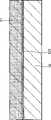
本发明在导电金属扩散抑制层124上形成厚度250nm的绝缘体涂布膜(栅极绝缘膜)133。利用该绝缘体涂布膜133把栅极电极12与透明树脂膜11之间的间隙112填埋,且能够提供不反映栅极电极12表面凹凸的具有Ra是0.30nm、峰-谷值是3.55nm平坦表面的栅极绝缘膜。图17是在该栅极电极上形成绝缘体涂布膜的栅极绝缘膜的结构,并表示观察剖面状况的电子显微镜照片。如图17所示,了解到形成不依赖于基底粗糙度的平坦表面。In the present invention, an insulator coating film (gate insulating film) 133 with a thickness of 250 nm is formed on the conductive metal
其结果是,能够使在栅极绝缘膜上形成的半导体层不产生由栅极电极12引起的凹凸地形成薄膜晶体管(TFT)。由此,能够大幅度提高载流子的移动度,而且在栅极绝缘膜的成膜工序中省略了用于形成CVD电介质膜的CVD工序,以简易的涂布工序进行成膜,能够实现工序的简略化。As a result, a thin film transistor (TFT) can be formed without causing unevenness due to the
下面使用图来说明上述第二实施例薄膜晶体管的形成方法。Next, the method of forming the thin film transistor of the second embodiment described above will be described using the drawings.
图11~图15是把第二实施例薄膜晶体管的制造方法按工序顺序表示的模式图。首先参照图11,作为基板而准备玻璃基板10。作为该玻璃基板也可以是为了形成30英寸以上大型画面的大型基板。把该玻璃基板进行0.5%体积的氢氟酸水溶液10秒钟处理,用纯水进行水洗来把表面的污染洗净除去。然后,通过向纯水添加氢氧化钠而把pH控制在10的水溶液中以0.1%体积的浓度溶解硅烷偶合剂即氨基丙基乙氧基硅烷,把玻璃基板10以这样的硅烷偶合剂溶液进行处理,即在室温下以硅烷偶合剂溶液浸渍30分钟,使玻璃基板10表面吸附硅烷偶合剂。然后在加热板上以110℃处理60分钟,使硅烷偶合剂与玻璃基板10表面化学结合,变成基底贴紧层(厚度10nm)121。通过这样形成基底贴紧层121,实质上是在基板表面配置了氨基,能够制作金属络合物容易配位的结构。由于硅烷偶合剂通常是透明的,所以即使形成在玻璃基板10的整个面上也能够得到本发明的效果,且根据得到玻璃基板10与后工序使用的透明感光性树脂贴紧性的观点,优选。11 to 15 are schematic diagrams showing the manufacturing method of the thin film transistor of the second embodiment in order of steps. First, referring to FIG. 11 , a
在形成基底贴紧层121后,使用旋转器把阳性感光胶液向基底贴紧层121的表面涂布,通过在加热板上以100℃进行120秒钟的加热预烘处理,形成具有2μm厚度的感光性透明树脂膜11。上述的阳性感光胶液使用专利文献4记载的含有碱可溶性脂环烯烃类树脂的。作为形成透明膜的有机材料,能够使用从由丙烯类树脂、硅类树脂、氟类树脂、聚酰亚胺类树脂、聚烯烃类树脂、脂环式烯烃类树脂和环氧类树脂构成的群中选择的透明树脂。但按照使以后的工序变容易的观点,作为透明膜以感光性透明树脂膜为适合,特别是如专利文献4或专利文献5所详述的那样,优选使用感光性透明树脂组成物。After forming the
参照图12,形成感光性透明树脂膜11后,利用掩膜对准器并经由掩膜图形把g、h、i线的混合光有选择地向感光性透明树脂膜11照射。然后,使用0.3%重量的氢氧化四甲基铵水溶液进行90秒的显影,之后用纯水进行60秒的冲洗处理,在玻璃基板10上形成具有规定图形的槽。然后在氮环境中进行230℃、60分钟的热处理,使感光性透明树脂膜11固化。接着把它在氯化钯盐酸水溶液(氯化钯0.005%体积、盐酸0.01%体积)中以室温浸渍3分钟,再用还原剂(上村工业(株)制还原剂MAB-2)处理水洗,在形成的槽内有选择地付与钯催化剂(催化剂层:厚度10~50nm)122。Referring to FIG. 12, after the photosensitive
参照图13,把被付与了钯催化剂122的玻璃基板10浸渍在铜非电解镀层液(上村工业(株)制PGT)中,在所述槽内有选择地把铜层123(厚度1.9μm)作为导电金属层形成。铜层123优选为仅以接续的扩散抑制膜(导电金属扩散抑制层)124膜厚度的量,并且在比感光性透明树脂膜11的表面高度低的位置完成处理。然后,浸渍在镍非电解镀层液中,在铜层123上形成由镍形成的扩散抑制膜124(厚度0.1μm)。Referring to Fig. 13, the
参照图14,接着,从栅极电极12表面延伸到感光性透明树脂膜11表面地涂布绝缘体膜以形成栅极绝缘膜133。该栅极绝缘膜133是如下得到的:涂布把Si有机化合物即有机硅氧烷溶解在有机溶剂(丙二醇单甲醚)中的液体,以120℃在大气中保持90秒使干燥,接着在大气中(也可以在氮气中)以180℃进行1小时烧制。然后利用公知的PECVD法连续堆积非晶硅膜141、n+型非晶硅膜142,利用光刻法和公知的RIE法把栅极电极12上及其周边部除去,把非晶硅膜的一部分除去。Referring to FIG. 14 , next, an insulator film is applied to extend from the surface of the
参照图15,接着利用公知的喷溅法等按Ti、Al、Ti的顺序进行成膜以作为源极电极和漏极电极,利用光刻法形成图形,形成源极电极15和漏极电极16。然后,把形成的源极电极15和漏极电极16作为掩膜而利用公知的方法腐蚀n+型非晶硅膜142,把源极区域与漏极区域进行分离。接着利用公知的PECVD法形成作为保护膜的硅氮化膜(未图示),完成第二实施例的薄膜晶体管。Referring to Fig. 15, then utilize known sputtering method etc. to carry out film-forming in the order of Ti, Al, Ti as source electrode and drain electrode, utilize photolithography to form pattern,
[第三实施例][Third embodiment]
使用图16说明适用液晶显示装置的第三实施例薄膜晶体管的形成方法。A method of forming a thin film transistor according to a third embodiment applicable to a liquid crystal display device will be described with reference to FIG. 16 .
在第二实施例说明的薄膜晶体管的制造方法中,在铜层123上形成镍的扩散抑制膜124(厚度0.1μm),形成栅极电极12后,从栅极电极12表面达到透明树脂膜11表面整个区域地在微波激发RLSA等离子处理装置中使Si3N4膜(氮化硅电介质膜)132进行CVD生长,形成绝缘膜。接着在Si3N4膜整体上涂布形成绝缘体涂布膜131,形成栅极绝缘膜13。该绝缘体涂布膜131是如下得到的:涂布把Si有机化合物即有机硅氧烷溶解在有机溶剂(丙二醇单甲醚)中的液体,以120℃在大气中保持90秒使干燥,接着在大气中(也可以在氮气中)以180℃进行1小时烧制。通过形成该绝缘体涂布膜131则能够降低使向其下的表面粗糙度大的栅极电极12上由CVD生长产生的绝缘膜(Si3N4膜132)表面的表面粗糙度,能够降低通道层即栅极绝缘膜与半导体层界面的粗糙度。图16是这时薄膜晶体管的剖面图。In the manufacturing method of the thin film transistor described in the second embodiment, the diffusion suppressing film 124 (thickness 0.1 μm) of nickel is formed on the
上述实施例仅对适合液晶显示装置的情况进行了说明,但本发明能够适用以有机EL显示装置为主的构成平面显示器屏的各种基板和其他配线基板。The above-mentioned embodiments have only been described as being suitable for liquid crystal display devices, but the present invention can be applied to various substrates and other wiring substrates constituting flat panel displays, mainly organic EL display devices.
作为构成配线的材料,不仅是铜、银,例如也可以形成铟-锡氧化物(ITO)等金属氧化物那样的导电性膜。As a material constituting the wiring, not only copper and silver but also conductive films such as metal oxides such as indium-tin oxide (ITO) may be formed.
本发明适用于液晶显示装置、有机EL装置、无机EL装置等显示装置,能够把这些显示装置大型化,而且还能够适用于显示装置以外的配线。The present invention is applicable to display devices such as liquid crystal display devices, organic EL devices, and inorganic EL devices, and can enlarge these display devices, and can also be applied to wiring other than display devices.
Claims (40)
Applications Claiming Priority (3)
| Application Number | Priority Date | Filing Date | Title |
|---|---|---|---|
| JP2006257848 | 2006-09-22 | ||
| JP257848/2006 | 2006-09-22 | ||
| JP313492/2006 | 2006-11-20 |
Publications (1)
| Publication Number | Publication Date |
|---|---|
| CN101506985Atrue CN101506985A (en) | 2009-08-12 |
Family
ID=40977789
Family Applications (1)
| Application Number | Title | Priority Date | Filing Date |
|---|---|---|---|
| CNA2007800310951APendingCN101506985A (en) | 2006-09-22 | 2007-09-21 | Semiconductor device and semiconductor device manufacturing method |
Country Status (1)
| Country | Link |
|---|---|
| CN (1) | CN101506985A (en) |
Cited By (8)
| Publication number | Priority date | Publication date | Assignee | Title |
|---|---|---|---|---|
| CN101807004A (en)* | 2010-03-08 | 2010-08-18 | 彩虹集团电子股份有限公司 | Method for manufacturing working printing plate for production of color kinescope screen printing plate |
| CN103000692A (en)* | 2011-09-14 | 2013-03-27 | 鸿富锦精密工业(深圳)有限公司 | Thin-film transistor structure and manufacturing method thereof |
| CN103299429A (en)* | 2010-12-27 | 2013-09-11 | 夏普株式会社 | Active matrix substrate, method for manufacturing same, and display panel |
| CN103489922A (en)* | 2013-09-30 | 2014-01-01 | 京东方科技集团股份有限公司 | Thin film transistor and preparation method thereof, array substrate and preparation method thereof and display device |
| CN105789221A (en)* | 2009-03-27 | 2016-07-20 | 株式会社半导体能源研究所 | Semiconductor device |
| CN110379715A (en)* | 2014-08-26 | 2019-10-25 | 株式会社尼康 | Transfer substrate |
| WO2020187237A1 (en)* | 2019-03-20 | 2020-09-24 | 京东方科技集团股份有限公司 | Thin film transistor and manufacturing method therefor, and display device |
| US11282964B2 (en) | 2017-12-07 | 2022-03-22 | Semiconductor Energy Laboratory Co., Ltd. | Semiconductor device |
- 2007
- 2007-09-21CNCNA2007800310951Apatent/CN101506985A/enactivePending
Cited By (14)
| Publication number | Priority date | Publication date | Assignee | Title |
|---|---|---|---|---|
| CN105789221A (en)* | 2009-03-27 | 2016-07-20 | 株式会社半导体能源研究所 | Semiconductor device |
| CN101807004B (en)* | 2010-03-08 | 2012-07-11 | 彩虹集团电子股份有限公司 | Method for manufacturing working printing plate for production of color kinescope screen printing plate |
| CN101807004A (en)* | 2010-03-08 | 2010-08-18 | 彩虹集团电子股份有限公司 | Method for manufacturing working printing plate for production of color kinescope screen printing plate |
| CN103299429B (en)* | 2010-12-27 | 2016-08-10 | 夏普株式会社 | Active-matrix substrate and manufacture method thereof and display floater |
| CN103299429A (en)* | 2010-12-27 | 2013-09-11 | 夏普株式会社 | Active matrix substrate, method for manufacturing same, and display panel |
| CN103000692A (en)* | 2011-09-14 | 2013-03-27 | 鸿富锦精密工业(深圳)有限公司 | Thin-film transistor structure and manufacturing method thereof |
| CN103489922A (en)* | 2013-09-30 | 2014-01-01 | 京东方科技集团股份有限公司 | Thin film transistor and preparation method thereof, array substrate and preparation method thereof and display device |
| CN103489922B (en)* | 2013-09-30 | 2017-01-18 | 京东方科技集团股份有限公司 | Thin film transistor and preparation method thereof, array substrate and preparation method thereof and display device |
| CN110379715A (en)* | 2014-08-26 | 2019-10-25 | 株式会社尼康 | Transfer substrate |
| CN111128707A (en)* | 2014-08-26 | 2020-05-08 | 株式会社尼康 | Element manufacturing method and transfer substrate |
| CN111128707B (en)* | 2014-08-26 | 2023-06-16 | 株式会社尼康 | Method for manufacturing element and transfer substrate |
| US11282964B2 (en) | 2017-12-07 | 2022-03-22 | Semiconductor Energy Laboratory Co., Ltd. | Semiconductor device |
| US11784259B2 (en) | 2017-12-07 | 2023-10-10 | Semiconductor Energy Laboratory Co., Ltd. | Oxide semiconductor device |
| WO2020187237A1 (en)* | 2019-03-20 | 2020-09-24 | 京东方科技集团股份有限公司 | Thin film transistor and manufacturing method therefor, and display device |
Similar Documents
| Publication | Publication Date | Title |
|---|---|---|
| US11289464B2 (en) | Display substrate, method for fabricating the same, and display device | |
| CN101506985A (en) | Semiconductor device and semiconductor device manufacturing method | |
| CN104393001B (en) | Thin-film transistor array base-plate and preparation method thereof, display device | |
| EP2096678A1 (en) | Semiconductor device and method for manufacturing semiconductor device | |
| US20090278134A1 (en) | Semiconductor device and method of manufacturing the semiconductor device | |
| US9632382B2 (en) | Array substrate comprising a barrier layer pattern and the method for manufacturing the same, and liquid crystal display device | |
| CN104409360A (en) | Thin film transistor and forming method thereof | |
| CN103000693B (en) | Thin-film transistor, display part, manufacturing method of display part, and display device | |
| US11877484B2 (en) | Display panel, preparation method for display panel and display device | |
| CN100487887C (en) | Thin film transistor array panel and a manufacturing method thereof | |
| WO2016115824A1 (en) | Thin film transistor and array substrate, and manufacturing method therefor | |
| CN110112142A (en) | Array substrate and its manufacturing method, display panel and electronic device | |
| KR20120075048A (en) | Thin film transistor substrate and method for manufacturing thereof | |
| CN104465670B (en) | A kind of array base palte and preparation method thereof, display device | |
| JPH0862628A (en) | Liquid crystal display device and manufacturing method thereof | |
| CN107591413A (en) | A kind of preparation method of TFT substrate, TFT substrate and OLED display panel | |
| US20070020836A1 (en) | Method for manufacturing thin film transistor substrate | |
| KR20090078527A (en) | Display board | |
| JPH11202368A5 (en) | ||
| CN106252419A (en) | Thin film transistor (TFT) and manufacture method, array base palte and display device | |
| KR100303443B1 (en) | Thin film transistor substrate for liquid crystal display and a manufacturing method thereof | |
| KR101325665B1 (en) | Array substrate and method for fabricating the same | |
| KR101868867B1 (en) | Fabricating method of flexible display device | |
| CN111681990A (en) | Method for preparing a display substrate, display substrate and display device | |
| CN105118838B (en) | A kind of array base palte and preparation method thereof, display panel, display device |
Legal Events
| Date | Code | Title | Description |
|---|---|---|---|
| C06 | Publication | ||
| PB01 | Publication | ||
| C10 | Entry into substantive examination | ||
| SE01 | Entry into force of request for substantive examination | ||
| ASS | Succession or assignment of patent right | Free format text:FORMER OWNER: NIPPON ZEON CO., LTD. Owner name:NIPPON ZEON CO., LTD. Free format text:FORMER OWNER: NAT UNIVERSITY CORP. TOHOKU UNI Effective date:20100816 | |
| C41 | Transfer of patent application or patent right or utility model | ||
| COR | Change of bibliographic data | Free format text:CORRECT: ADDRESS; FROM: MIYAGI, JAPAN TO: TOKYO, JAPAN | |
| TA01 | Transfer of patent application right | Effective date of registration:20100816 Address after:Tokyo, Japan, Japan Applicant after:Nippon Zeon Co., Ltd. Address before:Miyagi Prefecture in Japan Applicant before:Nat University Corp. Tohoku Uni Co-applicant before:Nippon Zeon Co., Ltd. | |
| C02 | Deemed withdrawal of patent application after publication (patent law 2001) | ||
| WD01 | Invention patent application deemed withdrawn after publication | Open date:20090812 |