CN101506974B - Latch-free Vertical Transient Voltage Suppression Diode Array Structure Formed by Trench Isolation - Google Patents
Latch-free Vertical Transient Voltage Suppression Diode Array Structure Formed by Trench IsolationDownload PDFInfo
- Publication number
- CN101506974B CN101506974BCN2007800317560ACN200780031756ACN101506974BCN 101506974 BCN101506974 BCN 101506974BCN 2007800317560 ACN2007800317560 ACN 2007800317560ACN 200780031756 ACN200780031756 ACN 200780031756ACN 101506974 BCN101506974 BCN 101506974B
- Authority
- CN
- China
- Prior art keywords
- diode
- type
- array structure
- several
- semiconductor substrate
- Prior art date
- Legal status (The legal status is an assumption and is not a legal conclusion. Google has not performed a legal analysis and makes no representation as to the accuracy of the status listed.)
- Expired - Fee Related
Links
Images


Classifications
- H—ELECTRICITY
- H10—SEMICONDUCTOR DEVICES; ELECTRIC SOLID-STATE DEVICES NOT OTHERWISE PROVIDED FOR
- H10D—INORGANIC ELECTRIC SEMICONDUCTOR DEVICES
- H10D8/00—Diodes
- H—ELECTRICITY
- H10—SEMICONDUCTOR DEVICES; ELECTRIC SOLID-STATE DEVICES NOT OTHERWISE PROVIDED FOR
- H10D—INORGANIC ELECTRIC SEMICONDUCTOR DEVICES
- H10D30/00—Field-effect transistors [FET]
- H10D30/01—Manufacture or treatment
- H10D30/021—Manufacture or treatment of FETs having insulated gates [IGFET]
- H10D30/028—Manufacture or treatment of FETs having insulated gates [IGFET] of double-diffused metal oxide semiconductor [DMOS] FETs
- H10D30/0291—Manufacture or treatment of FETs having insulated gates [IGFET] of double-diffused metal oxide semiconductor [DMOS] FETs of vertical DMOS [VDMOS] FETs
- H10D30/0295—Manufacture or treatment of FETs having insulated gates [IGFET] of double-diffused metal oxide semiconductor [DMOS] FETs of vertical DMOS [VDMOS] FETs using recessing of the source electrodes
- H—ELECTRICITY
- H10—SEMICONDUCTOR DEVICES; ELECTRIC SOLID-STATE DEVICES NOT OTHERWISE PROVIDED FOR
- H10D—INORGANIC ELECTRIC SEMICONDUCTOR DEVICES
- H10D30/00—Field-effect transistors [FET]
- H10D30/01—Manufacture or treatment
- H10D30/021—Manufacture or treatment of FETs having insulated gates [IGFET]
- H10D30/028—Manufacture or treatment of FETs having insulated gates [IGFET] of double-diffused metal oxide semiconductor [DMOS] FETs
- H10D30/0291—Manufacture or treatment of FETs having insulated gates [IGFET] of double-diffused metal oxide semiconductor [DMOS] FETs of vertical DMOS [VDMOS] FETs
- H10D30/0297—Manufacture or treatment of FETs having insulated gates [IGFET] of double-diffused metal oxide semiconductor [DMOS] FETs of vertical DMOS [VDMOS] FETs using recessing of the gate electrodes, e.g. to form trench gate electrodes
- H—ELECTRICITY
- H10—SEMICONDUCTOR DEVICES; ELECTRIC SOLID-STATE DEVICES NOT OTHERWISE PROVIDED FOR
- H10D—INORGANIC ELECTRIC SEMICONDUCTOR DEVICES
- H10D30/00—Field-effect transistors [FET]
- H10D30/60—Insulated-gate field-effect transistors [IGFET]
- H10D30/64—Double-diffused metal-oxide semiconductor [DMOS] FETs
- H10D30/66—Vertical DMOS [VDMOS] FETs
- H10D30/665—Vertical DMOS [VDMOS] FETs having edge termination structures
- H—ELECTRICITY
- H10—SEMICONDUCTOR DEVICES; ELECTRIC SOLID-STATE DEVICES NOT OTHERWISE PROVIDED FOR
- H10D—INORGANIC ELECTRIC SEMICONDUCTOR DEVICES
- H10D64/00—Electrodes of devices having potential barriers
- H10D64/111—Field plates
- H10D64/117—Recessed field plates, e.g. trench field plates or buried field plates
- H—ELECTRICITY
- H10—SEMICONDUCTOR DEVICES; ELECTRIC SOLID-STATE DEVICES NOT OTHERWISE PROVIDED FOR
- H10D—INORGANIC ELECTRIC SEMICONDUCTOR DEVICES
- H10D84/00—Integrated devices formed in or on semiconductor substrates that comprise only semiconducting layers, e.g. on Si wafers or on GaAs-on-Si wafers
- H10D84/101—Integrated devices comprising main components and built-in components, e.g. IGBT having built-in freewheel diode
- H10D84/151—LDMOS having built-in components
- H10D84/156—LDMOS having built-in components the built-in components being Schottky barrier diodes
- H—ELECTRICITY
- H10—SEMICONDUCTOR DEVICES; ELECTRIC SOLID-STATE DEVICES NOT OTHERWISE PROVIDED FOR
- H10D—INORGANIC ELECTRIC SEMICONDUCTOR DEVICES
- H10D89/00—Aspects of integrated devices not covered by groups H10D84/00 - H10D88/00
- H—ELECTRICITY
- H10—SEMICONDUCTOR DEVICES; ELECTRIC SOLID-STATE DEVICES NOT OTHERWISE PROVIDED FOR
- H10D—INORGANIC ELECTRIC SEMICONDUCTOR DEVICES
- H10D62/00—Semiconductor bodies, or regions thereof, of devices having potential barriers
- H10D62/10—Shapes, relative sizes or dispositions of the regions of the semiconductor bodies; Shapes of the semiconductor bodies
- H10D62/102—Constructional design considerations for preventing surface leakage or controlling electric field concentration
- H10D62/103—Constructional design considerations for preventing surface leakage or controlling electric field concentration for increasing or controlling the breakdown voltage of reverse-biased devices
- H10D62/105—Constructional design considerations for preventing surface leakage or controlling electric field concentration for increasing or controlling the breakdown voltage of reverse-biased devices by having particular doping profiles, shapes or arrangements of PN junctions; by having supplementary regions, e.g. junction termination extension [JTE]
- H10D62/106—Constructional design considerations for preventing surface leakage or controlling electric field concentration for increasing or controlling the breakdown voltage of reverse-biased devices by having particular doping profiles, shapes or arrangements of PN junctions; by having supplementary regions, e.g. junction termination extension [JTE] having supplementary regions doped oppositely to or in rectifying contact with regions of the semiconductor bodies, e.g. guard rings with PN or Schottky junctions
- H10D62/107—Buried supplementary regions, e.g. buried guard rings
- H—ELECTRICITY
- H10—SEMICONDUCTOR DEVICES; ELECTRIC SOLID-STATE DEVICES NOT OTHERWISE PROVIDED FOR
- H10D—INORGANIC ELECTRIC SEMICONDUCTOR DEVICES
- H10D62/00—Semiconductor bodies, or regions thereof, of devices having potential barriers
- H10D62/10—Shapes, relative sizes or dispositions of the regions of the semiconductor bodies; Shapes of the semiconductor bodies
- H10D62/17—Semiconductor regions connected to electrodes not carrying current to be rectified, amplified or switched, e.g. channel regions
- H10D62/393—Body regions of DMOS transistors or IGBTs
Landscapes
- Metal-Oxide And Bipolar Metal-Oxide Semiconductor Integrated Circuits (AREA)
- Semiconductor Integrated Circuits (AREA)
- Bipolar Integrated Circuits (AREA)
- Element Separation (AREA)
Abstract
Description
Translated fromChinese技术领域technical field
本发明涉及一种瞬态电压抑制二极管(transient voltage suppressing;TVS)的电路结构及其制造方法。尤其涉及一种使用沟槽隔离技术来制造垂直瞬态电压抑制二极管阵列的改良的电路结构及其制造方法,用以解决闭锁效应这一技术性上的困难。The invention relates to a circuit structure of a transient voltage suppressing diode (transient voltage suppressing; TVS) and a manufacturing method thereof. In particular, it relates to an improved circuit structure and a manufacturing method for manufacturing a vertical transient voltage suppression diode array by using trench isolation technology to solve the technical difficulty of latch-up effect.
背景技术Background technique
传统技术中,对于瞬态电压抑制二极管(TVS)阵列结构的设计与制造方法一直存在着一种技术性上的困难。该技术性的困难,也就是指在瞬态电压抑制二极管阵列结构中的多个PN结二极管通常是使用标准的互补式金属氧化物半导体(CMOS)制程步骤来形成在半导体衬底上,因此,往往会产生固有的PNP寄生晶体管与NPN寄生晶体管。在静电放电(electrostatic discharge;ESD)的情况下或发生瞬态电压时,会有较大的电压施加于瞬态电压抑制二极管阵列结构,寄生NPN晶体管或寄生PNP晶体管就会开启并触发闭锁(latch-up)效应,而导致一种突然且猛烈的电压骤回(snapback)现象。这种突然且猛烈的骤回现象极有可能会对于系统的稳定性产生不可预期的影响甚至造成损害。另外,在瞬态电压抑制二极管阵列结构中的寄生NPN晶体管或寄生PNP晶体管的闭锁效应可能会进一步导致其它突如其然或不可预期的电压-电流瞬态(transient)变化。然而,由瞬态电压抑制二极管阵列结构中寄生NPN晶体管或寄生PNP晶体管的闭锁现象所造成的技术性难题却无法轻易地获得解决。In the traditional technology, there has always been a technical difficulty in the design and manufacture of the transient voltage suppressor diode (TVS) array structure. This technical difficulty refers to the fact that multiple PN junction diodes in a TVS diode array structure are usually formed on a semiconductor substrate using standard complementary metal-oxide-semiconductor (CMOS) process steps, and therefore, often There will be inherent PNP parasitic transistors and NPN parasitic transistors. In the case of electrostatic discharge (ESD) or transient voltage, a large voltage will be applied to the transient voltage suppression diode array structure, and the parasitic NPN transistor or parasitic PNP transistor will be turned on and trigger the latch (latch -up) effect, resulting in a sudden and violent voltage snapback (snapback) phenomenon. This sudden and violent snapback phenomenon is very likely to have an unexpected impact or even cause damage to the stability of the system. In addition, the latch-up effect of parasitic NPN transistors or parasitic PNP transistors in the TVS diode array structure may further cause other sudden or unexpected voltage-current transient changes. However, technical problems caused by the latch-up phenomenon of parasitic NPN transistors or parasitic PNP transistors in the TVS diode array structure cannot be easily solved.
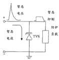
特别是,瞬态电压抑制二极管通常用于防止集成电路遭受突然的过电压而产生损害。一种集成电路被设计为在正常范围的电压下运行。然而,在许多情况下,例如静电放电时,电流会快速地产生瞬态变化并且减轻,而高电压可能就会突如其然且无法控制地对于电路造成冲击。当发生这种过电压的情况时,就需要瞬态电压抑制二极管去执行防护功能来避免可能会对集成电路造成的伤害。随着越来越多的器件是通过集成电路来实现的,集成电路将变得很容易受到过电压的损害,而对于瞬态电压抑制二极管的损害防护的需求也将随之增加。瞬态电压抑制二极管的典型应用包含有通用串行总线(USB)电源与数据线防护、数字影像接口(Digital video interface)、高速以太网络(Ethernet)、笔记本计算机、显示器以及平面显示器等。In particular, TVS diodes are commonly used to protect integrated circuits from damage caused by sudden overvoltages. An integrated circuit is designed to operate at a normal range of voltages. However, in many situations, such as electrostatic discharge, where the current transients and eases quickly, high voltages can shock circuits suddenly and uncontrollably. When such an overvoltage occurs, a transient voltage suppression diode is required to perform a protective function to avoid possible damage to the integrated circuit. As more and more devices are implemented in integrated circuits, integrated circuits will become more vulnerable to overvoltage damage, and the need for damage protection of transient voltage suppressor diodes will also increase. Typical applications of TVS diodes include Universal Serial Bus (USB) power and data line protection, digital video interface (Digital video interface), high-speed Ethernet (Ethernet), notebook computers, monitors, and flat-panel displays.
图1A与图1B分别显示一种瞬态电压抑制二极管器件的电路图与电流-电压图。一种理想的瞬态电压抑制二极管应当可以在输入电压Vin小于击穿电压Vb时,将电流全部加以阻挡,即获得零电流(zero-current),从而最小化漏电流。再者,理想上,当输入电压Vin大于击穿电压Vb时,瞬态电压抑制二极管在这种情况下应该具有接近零的电阻,以致于瞬态电压能够被有效地抑制下来。一种利用具有击穿电压的PN结器件来实现的瞬态电压抑制二极管可以在瞬态输入电压超过击穿电压的情况时,允许电流传导而获得瞬态电压的防护。然而,如图1B中所示,由于PN结类型的瞬态电压抑制二极管具有高电阻,因此不具有少数载子并且其抑制效果不佳。同样地,利用双极型NPN/PNP来实现的瞬态电压抑制二极管具有双极型晶体管的雪崩触发(avalanche-triggered)启动,雪崩电流会随双极增益而放大,而基极将会涌进少数载子,且双极型瞬态电压抑制二极管能够获得较佳的抑制电压。1A and 1B respectively show a circuit diagram and a current-voltage diagram of a TVS diode device. An ideal TVS diode should be able to block all current when the input voltage Vin is lower than the breakdown voltage Vb, that is, to obtain zero-current, thereby minimizing leakage current. Furthermore, ideally, when the input voltage Vin is greater than the breakdown voltage Vb, the TVS diode should have a resistance close to zero in this case, so that the transient voltage can be effectively suppressed. A transient voltage suppression diode implemented by a PN junction device with a breakdown voltage can allow current conduction to obtain transient voltage protection when the transient input voltage exceeds the breakdown voltage. However, as shown in FIG. 1B , since the PN junction type TVS diode has high resistance, it does not have minority carriers and its suppression effect is not good. Similarly, a TVS diode implemented using a bipolar NPN/PNP has avalanche-triggered start-up of a bipolar transistor, the avalanche current will be amplified by the bipolar gain, and the base will flood into Minority carriers, and bipolar transient voltage suppression diodes can obtain better suppression voltage.
随着电子技术的发展,越来越多的器件与应用需要瞬态电压抑制二极管阵列结构来提供静电放电(ESD)防护,特别是针对于高带宽数据总线的防护。图2A为一种四沟道瞬态电压抑制二极管的电路图;图2B是瞬态电压抑制二极管阵列结构的侧面剖视图,仅仅显示了该阵列器件的核心部份。如图2A与图2B所示的瞬态电压抑制二极管阵列包含串联的若干个高压侧控向二极管(high-side steering diode)与低压侧控向二极管(low-side steering diode),其中高压侧控向二极管连接到Vcc,低压侧控向二极管连接到接地电位。高压侧控向二极管与低压侧控向二极管还并联一主线齐纳二极管(Zenerdiode),控向二极管比齐纳二极管小了许多并具有较低的结电容(junctioncapacitance)。此外,如图2C所示,这样的实施方法进一步产生另一个问题,也就是由于寄生NPN晶体管与寄生PNP晶体管所导致的硅控整流器(SCR)操作产生的闭锁效应。主线齐纳二极管击穿会触发其上的寄生NPN晶体管开启,进一步开启硅控整流器而造成闭锁效应。在高温时,即使寄生NPN晶体管并未开启,但流经寄生NPN晶体管的NP结的高的漏电流可能也会开启硅控整流器,从而导致闭锁效应。为了抑制由寄生PNP晶体管与寄生NPN晶体管所导致的硅控整流器操作产生的闭锁效应,如图2B所示,实施在半导体衬底上的实际器件需要在半导体衬底上横向延伸一段距离,此距离可以高达10微米或更多,但是其抑制效果通常不够有效。With the development of electronic technology, more and more devices and applications require a transient voltage suppression diode array structure to provide electrostatic discharge (ESD) protection, especially for high-bandwidth data bus protection. FIG. 2A is a circuit diagram of a four-channel TVS diode; FIG. 2B is a side sectional view of a TVS diode array structure, showing only the core part of the array device. The TVS diode array shown in Figure 2A and Figure 2B includes several high-side steering diodes (high-side steering diode) and low-side steering diodes (low-side steering diode) connected in series, wherein the high-side steering diode The steering diode is connected to Vcc, and the low side steering diode is connected to ground potential. The high-voltage side steering diode and the low-voltage side steering diode are also connected in parallel with a main line Zener diode. The steering diode is much smaller than the Zener diode and has lower junction capacitance. In addition, as shown in FIG. 2C , such an implementation method further creates another problem, that is, the latch-up effect of the silicon controlled rectifier (SCR) operation due to the parasitic NPN transistor and the parasitic PNP transistor. Breakdown of the Zener diode on the main line will trigger the parasitic NPN transistor on it to turn on, further turning on the silicon controlled rectifier and causing a latch-up effect. At high temperature, a high leakage current flowing through the NP junction of the parasitic NPN transistor may turn on the silicon controlled rectifier even though the parasitic NPN transistor is not turned on, resulting in a latch-up effect. In order to suppress the latch-up effect caused by the operation of the silicon controlled rectifier caused by the parasitic PNP transistor and the parasitic NPN transistor, as shown in FIG. Can be as high as 10 microns or more, but the suppression is usually not effective enough.
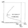
如图3A与图3B所示,其说明在以太网络差分保护电路(Ethernetdifferential protection circuit)由于寄生PNP晶体管上的闭锁效应所导致的特殊困难。在此以太网络防护电路中,Vcc与接地管脚都是以浮置(floating)方式设置的。然而,在这个设计中的寄生的硅控整流器结构并不足够弱,仍会导致如图3B所示的突变电压的骤回现象。这样的突发与强烈的骤回现象可能会对于系统的稳定性造成不可预期的影响甚至产生伤害。由于寄生PNP晶体管本来就存在于互补式金属氧化物半导体(CMOS)的制程中,且实际上Vcc与接地管脚浮置会让闭锁效应恶化,这些困难并无法轻易地获得解决。另外,也需要额外的埋入层(buried layers)来抑制寄生PNP晶体管的增益,这将导致复杂的器件结构与极高的制造成本。As shown in FIGS. 3A and 3B , it illustrates a particular difficulty in an Ethernet differential protection circuit due to latch-up effects on parasitic PNP transistors. In this Ethernet protection circuit, both the Vcc and ground pins are set in a floating manner. However, the parasitic SCR structure in this design is not weak enough to still cause the sudden voltage snapback phenomenon as shown in Figure 3B. Such a sudden and strong snapback phenomenon may cause unexpected impact or even damage to the stability of the system. Since the parasitic PNP transistors inherently exist in the complementary metal-oxide-semiconductor (CMOS) process, and the fact that the Vcc and ground pins are floating will worsen the latch-up effect, these difficulties cannot be easily solved. In addition, additional buried layers are required to suppress the gain of the parasitic PNP transistor, which will lead to complex device structure and high manufacturing cost.
因此,在电路设计和器件制造领域,仍然需要提供一种新颖改良的电路结构与制造方法来解决以上所述的各种困难。尤其是,目前仍然需要提供新颖改良的瞬态电压抑制二极管电路,以便能够有效率并容易地防止寄生PNP晶体管或寄生NPN晶体管的闭锁效应。Therefore, in the field of circuit design and device manufacturing, there is still a need to provide a novel and improved circuit structure and manufacturing method to solve the above-mentioned various difficulties. In particular, there is still a need to provide new and improved TVS diode circuits that can efficiently and easily prevent the latch-up effect of parasitic PNP transistors or parasitic NPN transistors.
发明内容Contents of the invention
本发明一方面在于提供一种崭新的与改良的瞬态电压抑制二极管阵列结构,通过使用闭锁隔离沟槽来防止寄生PNP晶体管或寄生NPN晶体管的闭锁效应,从而克服前述传统瞬态电压抑制二极管阵列所造成的诸多困难与限制。One aspect of the present invention is to provide a brand-new and improved TVS diode array structure, which prevents the latch-up effect of parasitic PNP transistors or parasitic NPN transistors by using lock-up isolation trenches, thereby overcoming the aforementioned traditional TVS diode arrays many difficulties and limitations.
本发明的另一方面在于提供一种使用隔离沟槽的无闭锁垂直瞬态电压抑制二极管阵列结构,将绝缘沟槽设置在二极管之间,使得相邻的二极管之间的横向距离能够被缩短,而不涉及闭锁效应。Another aspect of the present invention is to provide a latch-free vertical transient voltage suppression diode array structure using isolation trenches. The isolation trenches are arranged between the diodes, so that the lateral distance between adjacent diodes can be shortened, No latch-up effect is involved.
简单来说,本发明的一个较佳实施例公开一种瞬态电压抑制二极管阵列结构,其包含若干个形成在半导体衬底上的二极管,以作为不同导电类型的若干个掺杂区域,从而构成若干个PN结。该瞬态电压抑制二极管阵列结构进一步包含有设置在前述二极管之间的一绝缘沟槽,用于隔离并防止寄生PNP晶体管或寄生NPN晶体管所造成的闭锁效应(latch-up)。In brief, a preferred embodiment of the present invention discloses a transient voltage suppression diode array structure, which includes several diodes formed on a semiconductor substrate as several doped regions of different conductivity types, thereby forming Several PN junctions. The TVS diode array structure further includes an insulating trench disposed between the aforementioned diodes for isolating and preventing latch-up caused by parasitic PNP transistors or parasitic NPN transistors.
本发明进一步公开一种集成有瞬态电压抑制二极管阵列结构的电子器件的制造方法。此制造方法包含以下步骤:通过掺杂具有不同导电类型的若干个掺杂区域,在半导体衬底上制造瞬态电压抑制二极管阵列,从而在这些掺杂区域之间的PN结之间形成若干个二极管。此制造方法进一步包含以下步骤:在上述掺杂区域之间形成绝缘沟槽,用来隔离掺杂区域,并用来防止在半导体衬底上不同导电类型的掺杂区域之间的寄生PNP晶体管或寄生NPN晶体管所引发的闭锁效应。The invention further discloses a manufacturing method of an electronic device integrated with a transient voltage suppression diode array structure. This manufacturing method includes the following steps: manufacturing a transient voltage suppression diode array on a semiconductor substrate by doping several doped regions with different conductivity types, thereby forming several PN junctions between these doped regions diode. This manufacturing method further includes the following steps: forming an insulating trench between the above-mentioned doped regions, used to isolate the doped regions, and used to prevent parasitic PNP transistors or parasitics between doped regions of different conductivity types on the semiconductor substrate. Latch-up effect caused by NPN transistor.
进一步地,一种瞬态电压抑制二极管阵列结构的制造方法,包含:Further, a method for manufacturing a transient voltage suppression diode array structure, comprising:
在半导体衬底上具有第一导电类型的外延层上开设若干个绝缘沟槽,然后使用一体区掩膜在二个绝缘沟槽之间掺杂一具有第二导电类型的体区;以及使用一源极掩膜来植入若干个具有第一导电类型的掺杂区域,以构成若干个二极管,其中,所述的绝缘沟槽将二极管加以隔离,并防止寄生PNP晶体管或寄生NPN晶体管在该半导体衬底上不同导电类型的掺杂区域之间所引发的闭锁效应。Opening several insulating trenches on the epitaxial layer with the first conductivity type on the semiconductor substrate, and then using an integral region mask to dope a body region with the second conductivity type between the two insulating trenches; and using a The source mask is used to implant several doped regions with the first conductivity type to form several diodes, wherein the insulating trench isolates the diodes and prevents parasitic PNP transistors or parasitic NPN transistors in the semiconductor The latch-up effect induced between doped regions of different conductivity types on a substrate.
所述的一种瞬态电压抑制二极管阵列结构的制造方法进一步包含以下步骤:使用一接触掩膜植入远离该体区的若干个具有第二导电类型的掺杂区域,用来与该外延层构成若干个高压侧二极管,并利用通过所述绝缘沟槽的若干个输入/输出接触衬垫来连接到被体区包围的低压侧二极管。The method for manufacturing a transient voltage suppression diode array structure further includes the following steps: using a contact mask to implant a plurality of doped regions with the second conductivity type far away from the body region for contact with the epitaxial layer A number of high side diodes are formed and connected to the low side diodes surrounded by the body region by means of a number of input/output contact pads through the insulating trenches.
所述植入若干个具有第二导电类型的掺杂区域,以及使用一源极掩膜来植入若干个具有第一导电类型的掺杂区域,从而构成若干个二极管的步骤还进一步包含有以下步骤:形成一具有较大宽度的齐纳掺杂区域,其中,该齐纳掺杂区域和该外延层中的体区形成垂直堆栈PN结,用以构成一齐纳二极管。The step of implanting several doped regions with the second conductivity type, and using a source mask to implant several doped regions with the first conductivity type, thereby forming several diodes further includes the following steps Step: forming a zener-doped region with a larger width, wherein the zener-doped region and the body region in the epitaxial layer form a vertically stacked PN junction to form a zener diode.
所述的开设若干个绝缘沟槽的步骤还进一步包含以下步骤:邻近该齐纳二极管开设若干个绝缘沟槽,将该齐纳二极管加以隔离,用以防止不同导电类型的掺杂区域之间的闭锁效应的发生。The step of opening several insulating trenches further includes the following steps: opening several insulating trenches adjacent to the Zener diode to isolate the Zener diode, so as to prevent interference between doped regions of different conductivity types. Lock-in effect occurs.
所述的一种瞬态电压抑制二极管阵列结构的制造方法进一步包含在该半导体衬底的下表面沉积一金属层,用来作为该瞬态电压抑制二极管阵列结构的电极。The manufacturing method of a transient voltage suppression diode array structure further includes depositing a metal layer on the lower surface of the semiconductor substrate, which is used as an electrode of the transient voltage suppression diode array structure.
所述的一种瞬态电压抑制二极管阵列结构的制造方法进一步包含在该半导体衬底的表面沉积一金属层,并对该金属层进行图案化,用来作为若干个输入/输出接触衬垫,并作为该瞬态电压抑制二极管阵列结构的电极,且该电极的导电类型和形成在该半导体衬底的下表面的电极的导电类型相反。The manufacturing method of a transient voltage suppression diode array structure further includes depositing a metal layer on the surface of the semiconductor substrate, and patterning the metal layer to serve as several input/output contact pads, And as an electrode of the transient voltage suppression diode array structure, and the conductivity type of the electrode is opposite to that of the electrode formed on the lower surface of the semiconductor substrate.
通过对照附图阅读对本发明的较佳实施例的详细描述,本发明的目的和优点对于本领域内的技术人员来说是显而易见的。Objects and advantages of this invention will become apparent to those skilled in the art from the detailed description of the preferred embodiment of the invention when read with the accompanying drawings.
附图说明Description of drawings
图式说明:Graphic description:
图1A是一种传统的瞬态电压抑制二极管器件的电路图,图1B是电流-电压(I-V)图,即电流对应电压图,用来说明瞬态电压抑制二极管器件的反向特性;Fig. 1A is a circuit diagram of a traditional TVS diode device, and Fig. 1B is a current-voltage (I-V) diagram, i.e. a current-corresponding voltage diagram, used to illustrate the reverse characteristic of the TVS diode device;
图2A是一种传统的瞬态电压抑制二极管阵列结构电路图,该瞬态电压抑制二极管阵列包含若干个连接输入/输出(I/O)衬垫的高压侧二极管与低压侧二极管,还具有一并联所述高压侧二极管与低压侧二极管的主线齐纳二极管;Fig. 2A is a circuit diagram of a traditional TVS diode array structure, the TVS diode array includes several high-side diodes and low-side diodes connected to the input/output (I/O) pad, and also has a parallel a main line zener diode of the high voltage side diode and the low voltage side diode;
图2B是应用了图2A所示的一种传统的瞬态电压抑制二极管阵列结构的侧面剖视图;Fig. 2B is a side sectional view of a traditional transient voltage suppression diode array structure shown in Fig. 2A;
图2C是图2B中器件的电位闭锁效应的等效电路图;Fig. 2 C is the equivalent circuit diagram of the potential blocking effect of device among Fig. 2 B;
图3A是一种根据如图2B所示的以太网络差分保护电路的电路图,该保护电路需要将Vcc与GND管脚浮置,且需要埋入层来抑制具有防护电路结构的寄生硅控整流器(SCR)的增益;FIG. 3A is a circuit diagram of an Ethernet differential protection circuit as shown in FIG. 2B. The protection circuit needs to float Vcc and GND pins, and a buried layer is required to suppress parasitic silicon controlled rectifiers ( SCR) gain;
图3B是一种用来说明一种静电放电防护或瞬态电压抑制二极管操作的电流-电压(I-V)图,当使用传统的瞬态电压抑制二极管阵列时,会导致不可预期的突发与强烈的骤回现象的发生;Figure 3B is a current-voltage (I-V) diagram illustrating the operation of an ESD protection or TVS diode, which can result in unexpected bursts and intense the occurrence of the snapback phenomenon;
图4是根据本发明所提供的一种使用沟槽隔离的瞬态电压抑制二极管阵列结构的侧面剖视图,其明显减少寄生NPN晶体管或寄生PNP晶体管的闭锁效应;4 is a side sectional view of a transient voltage suppression diode array structure using trench isolation provided according to the present invention, which can significantly reduce the latch-up effect of parasitic NPN transistors or parasitic PNP transistors;
图5是根据本发明所提供的另一种使用沟槽隔离的瞬态电压抑制二极管阵列结构的侧面剖视图,其明显减少寄生PNP或NPN晶体管的闭锁效应;以及5 is a side cross-sectional view of another TVS diode array structure using trench isolation provided according to the present invention, which can significantly reduce the latch-up effect of parasitic PNP or NPN transistors; and
图6是用以说明本发明的一种静电放电防护或瞬态电压抑制二极管操作的电流-电压(I-V)图,由于减少了闭锁效应,而可明显减轻骤回现象。6 is a current-voltage (I-V) diagram illustrating the operation of an ESD protection or transient voltage suppression diode of the present invention, which can significantly reduce the snapback phenomenon due to the reduction of latch-up effect.
具体实施方式Detailed ways
图4是根据本发明所提供的一种新颖改良的瞬态电压抑制二极管阵列结构的部份的侧面剖视图。如图所示,此部份的瞬态电压抑制二极管阵列结构100具有两个沟道,两沟道设置在N型衬底101的上表面的N型外延层105上,而N型衬底101的下表面则连接到施以电压Vcc的阳极端110。该瞬态电压抑制二极管阵列连接在设置在下表面的阳极端110与设置在连接接地电压的上表面上的阴极端120之间。瞬态电压抑制二极管阵列结构100进一步包含连接到第一输入输出(IO)端135的第一高压侧二极管125与第一低压侧二极管130。另外,瞬态电压抑制二极管阵列结构100进一步包含连接到第二输入输出(IO)端150的第二高压侧二极管140与第二低压侧二极管145。第一高压侧二极管125是形成来作为P型掺杂区域125-P与N型外延层105之间的PN结。第一低压侧二极管130是形成来作为N型掺杂区域135-N与设置在阴极端120下方的P型体区160之间的PN结,且第一输入输出(IO)衬垫135连接到第一低压侧二极管130的N型掺杂区域135-N,还连接到第一高压侧二极管125的P型掺杂区域125-P。第二低压侧二极管145是形成来作为N型掺杂区域145-N与设置在阴极端120下方的P型体区160之间的PN结,且第二输入输出(IO)衬垫150连接到第二低压侧二极管145的N型掺杂区域145-N,还连接到第二高压侧二极管140的P型掺杂区域140-P。较大区域的齐纳二极管170是由P型体区160与N型外延层105之间的PN结形成的。NPN晶体管能够被齐纳二极管170触发,且NPN晶体管是由N型射极区域155、P型体区160与N型衬底101所形成的,从而并不需要太大的电阻就可传导大的瞬态电流。另外,瞬态电压抑制二极管阵列结构100进一步包含第一绝缘沟槽180-1,其形成在第一高压侧二极管125与第一低压侧二极管130之间。瞬态电压抑制二极管阵列结构100进一步包含第二绝缘沟槽180-2,其形成在第二高压侧二极管140与第二低压侧二极管145之间。绝缘沟槽可以防止寄生NPN与PNP晶体管所造成的闭锁效应,而所述的寄生NPN与PNP晶体管是固有形成在由高压侧与低压侧二极管所形成的多个PN结之间的。FIG. 4 is a partial side cross-sectional view of a novel and improved TVS diode array structure provided by the present invention. As shown in the figure, the TVS diode array structure 100 of this part has two channels, and the two channels are arranged on the N-type epitaxial layer 105 on the upper surface of the N-type substrate 101, and the N-type substrate 101 The lower surface is connected to the anode terminal 110 to which the voltage Vcc is applied. The TVS diode array is connected between an anode terminal 110 provided on the lower surface and a cathode terminal 120 provided on the upper surface connected to a ground voltage. The TVS diode array structure 100 further includes a first high-side diode 125 and a first low-side diode 130 connected to a first input-output (IO) terminal 135 . In addition, the TVS diode array structure 100 further includes a second high-side diode 140 and a second low-side diode 145 connected to the second input-output (IO) terminal 150 . The first high-side diode 125 is formed as a PN junction between the P-type doped region 125 -P and the N-type epitaxial layer 105 . The first low-side diode 130 is formed as a PN junction between the N-type doped region 135-N and the P-type body region 160 disposed below the cathode terminal 120, and the first input-output (IO) pad 135 is connected to The N-type doped region 135 -N of the first low-side diode 130 is also connected to the P-type doped region 125 -P of the first high-side diode 125 . The second low-side diode 145 is formed as a PN junction between the N-type doped region 145-N and the P-type body region 160 disposed below the cathode terminal 120, and the second input-output (IO) pad 150 is connected to The N-type doped region 145 -N of the second low-side diode 145 is also connected to the P-type doped region 140 -P of the second high-side diode 140 . The larger area Zener diode 170 is formed by the PN junction between the P-type body region 160 and the N-type epitaxial layer 105 . The NPN transistor can be triggered by the Zener diode 170, and the NPN transistor is formed by the N-type emitter region 155, the P-type body region 160 and the N-type substrate 101, so that the large resistance can be conducted without too much resistance. transient current. In addition, the TVS diode array structure 100 further includes a first insulating trench 180 - 1 formed between the first high side diode 125 and the first low side diode 130 . The TVS diode array structure 100 further includes a second insulating trench 180 - 2 formed between the second high side diode 140 and the second low side diode 145 . The isolation trench prevents latch-up caused by parasitic NPN and PNP transistors inherently formed between multiple PN junctions formed by high-side and low-side diodes.
图5是根据本发明所提供的另一个新颖改良的实施方式的瞬态电压抑制二极管阵列结构的侧面剖视图。除了在器件100’中具有额外的若干个提供了更好的隔离作用的沟槽外,图5中的器件100’类似于图4中的器件100。沟槽180’-1与180’-2将低压侧二极管与主线齐纳二极管区域分隔开来,因此击穿横向NPN,而横向NPN是由N型区域155、P型体区160与低压侧二极管阴极区域135-N与145-N所构成。Fig. 5 is a side cross-sectional view of a transient voltage suppression diode array structure according to another novel and improved embodiment of the present invention. Device 100' in Figure 5 is similar to device 100 in Figure 4, except that there are additional trenches in device 100' that provide better isolation. Trenches 180'-1 and 180'-2 separate the low-side diode from the mainline Zener diode region, thus breaking down the lateral NPN, which is composed of the N-type region 155, the P-type body region 160 and the low-side The diode cathode regions 135-N and 145-N are formed.
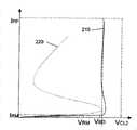
图6是用来说明本发明的一种静电放电(ESD)防护或瞬态电压抑制二极管操作的电流-电压(I-V)图,由于减低了闭锁效应,而可明显减轻骤回现象。如电流-电压图所示,电流-电压曲线220显示出在瞬态电压抑制二极管阵列结构中半导体衬底上不同掺杂区域之间所形成的寄生NPN晶体管或寄生PNP晶体管的闭锁效应,可能将导致以高电压及电流去开启寄生NPN晶体管或寄生PNP晶体管,因此引发一种突发的骤回现象。因为绝缘沟槽180-1与180-2的作用,闭锁效应将获得减轻,而且骤回现象会大大地减少。如电流-电压曲线210即是在发生骤回现象时所取得的曲线,其突发的电压变化会强烈地引起系统的不稳定。6 is a current-voltage (I-V) diagram illustrating the operation of an electrostatic discharge (ESD) protection or transient voltage suppression diode of the present invention, which can significantly reduce the snapback phenomenon due to reduced latch-up effect. As shown in the current-voltage diagram, the current-
虽然本发明以前述的实施例公开如上,然其并非用来限定本发明。在不脱离本发明的精神和范围内,所进行的改动与润饰,均属本发明的专利保护范围。关于本发明所界定的保护范围请参考权利要求书。Although the present invention is disclosed above with the foregoing embodiments, they are not intended to limit the present invention. Without departing from the spirit and scope of the present invention, the changes and modifications made all belong to the scope of patent protection of the present invention. Please refer to the claims for the scope of protection defined by the present invention.
Claims (11)
Applications Claiming Priority (3)
| Application Number | Priority Date | Filing Date | Title |
|---|---|---|---|
| US11/606,602 | 2006-11-30 | ||
| US11/606,602US7880223B2 (en) | 2005-02-11 | 2006-11-30 | Latch-up free vertical TVS diode array structure using trench isolation |
| PCT/US2007/024621WO2008066903A2 (en) | 2006-11-30 | 2007-11-30 | Latch-up free vertical tvs diode array structure using trench isolation |
Publications (2)
| Publication Number | Publication Date |
|---|---|
| CN101506974A CN101506974A (en) | 2009-08-12 |
| CN101506974Btrue CN101506974B (en) | 2013-04-10 |
Family
ID=39468519
Family Applications (1)
| Application Number | Title | Priority Date | Filing Date |
|---|---|---|---|
| CN2007800317560AExpired - Fee RelatedCN101506974B (en) | 2006-11-30 | 2007-11-30 | Latch-free Vertical Transient Voltage Suppression Diode Array Structure Formed by Trench Isolation |
Country Status (7)
| Country | Link |
|---|---|
| US (3) | US7880223B2 (en) |
| EP (1) | EP2089903A2 (en) |
| JP (1) | JP5333857B2 (en) |
| KR (1) | KR101394913B1 (en) |
| CN (1) | CN101506974B (en) |
| TW (1) | TWI405323B (en) |
| WO (1) | WO2008066903A2 (en) |
Families Citing this family (90)
| Publication number | Priority date | Publication date | Assignee | Title |
|---|---|---|---|---|
| US7781826B2 (en)* | 2006-11-16 | 2010-08-24 | Alpha & Omega Semiconductor, Ltd. | Circuit configuration and manufacturing processes for vertical transient voltage suppressor (TVS) and EMI filter |
| US8218276B2 (en)* | 2006-05-31 | 2012-07-10 | Alpha and Omega Semiconductor Inc. | Transient voltage suppressor (TVS) with improved clamping voltage |
| US9793256B2 (en)* | 2006-11-30 | 2017-10-17 | Alpha And Omega Semiconductor Incorporated | Optimized configurations to integrate steering diodes in low capacitance transient voltage suppressor (TVS) |
| US9202938B2 (en)* | 2006-11-30 | 2015-12-01 | Alpha And Omega Semiconductor Incorporated | Latch-up free vertical TVS diode array structure using trench isolation |
| DE102007024355B4 (en)* | 2007-05-24 | 2011-04-21 | Infineon Technologies Ag | Method for producing a protective structure |
| US8217419B2 (en)* | 2007-06-15 | 2012-07-10 | Rohm Co., Ltd. | Semiconductor device |
| US7579632B2 (en)* | 2007-09-21 | 2009-08-25 | Semiconductor Components Industries, L.L.C. | Multi-channel ESD device and method therefor |
| US7666751B2 (en)* | 2007-09-21 | 2010-02-23 | Semiconductor Components Industries, Llc | Method of forming a high capacitance diode and structure therefor |
| US7538395B2 (en)* | 2007-09-21 | 2009-05-26 | Semiconductor Components Industries, L.L.C. | Method of forming low capacitance ESD device and structure therefor |
| JP5365019B2 (en)* | 2008-02-08 | 2013-12-11 | 富士電機株式会社 | Semiconductor device |
| JP5264597B2 (en)* | 2008-04-03 | 2013-08-14 | 三菱電機株式会社 | Infrared detector and infrared solid-state imaging device |
| US7842969B2 (en)* | 2008-07-10 | 2010-11-30 | Semiconductor Components Industries, Llc | Low clamp voltage ESD device and method therefor |
| US7955941B2 (en)* | 2008-09-11 | 2011-06-07 | Semiconductor Components Industries, Llc | Method of forming an integrated semiconductor device and structure therefor |
| US7812367B2 (en)* | 2008-10-15 | 2010-10-12 | Semiconductor Components Industries, Llc | Two terminal low capacitance multi-channel ESD device |
| US8089095B2 (en) | 2008-10-15 | 2012-01-03 | Semiconductor Components Industries, Llc | Two terminal multi-channel ESD device and method therefor |
| CN101826716B (en)* | 2009-03-05 | 2014-05-21 | 万国半导体股份有限公司 | Low voltage transient voltage suppresser with potential barrier Zener diode |
| US8288839B2 (en) | 2009-04-30 | 2012-10-16 | Alpha & Omega Semiconductor, Inc. | Transient voltage suppressor having symmetrical breakdown voltages |
| US8558276B2 (en)* | 2009-06-17 | 2013-10-15 | Alpha And Omega Semiconductor, Inc. | Bottom source NMOS triggered zener clamp for configuring an ultra-low voltage transient voltage suppressor (TVS) |
| FR2953062B1 (en)* | 2009-11-24 | 2011-12-16 | St Microelectronics Tours Sas | LOW VOLTAGE BIDIRECTIONAL PROTECTION DIODE |
| US8169000B2 (en)* | 2010-07-15 | 2012-05-01 | Amazing Microelectronic Corp. | Lateral transient voltage suppressor with ultra low capacitance |
| US8237193B2 (en)* | 2010-07-15 | 2012-08-07 | Amazing Microelectronic Corp. | Lateral transient voltage suppressor for low-voltage applications |
| CN102376702B (en) | 2010-08-20 | 2014-09-17 | 半导体元件工业有限责任公司 | Two-terminal multi-channel ESD device and method thereof |
| US8431999B2 (en)* | 2011-03-25 | 2013-04-30 | Amazing Microelectronic Corp. | Low capacitance transient voltage suppressor |
| US8664080B2 (en)* | 2011-05-25 | 2014-03-04 | Texas Instruments Incorporated | Vertical ESD protection device |
| US8698196B2 (en) | 2011-06-28 | 2014-04-15 | Alpha And Omega Semiconductor Incorporated | Low capacitance transient voltage suppressor (TVS) with reduced clamping voltage |
| US8710627B2 (en) | 2011-06-28 | 2014-04-29 | Alpha And Omega Semiconductor Incorporated | Uni-directional transient voltage suppressor (TVS) |
| US8304838B1 (en)* | 2011-08-23 | 2012-11-06 | Amazing Microelectronics Corp. | Electrostatic discharge protection device structure |
| CN102290419B (en)* | 2011-08-24 | 2013-02-13 | 浙江大学 | Transient voltage suppressor based on Zener diode |
| CN102290417B (en)* | 2011-08-24 | 2012-10-24 | 浙江大学 | Transient voltage suppressor based on DTSCR (Dual Triggered Silicon Controlled Rectifier) |
| JP5749616B2 (en)* | 2011-09-27 | 2015-07-15 | セミコンダクター・コンポーネンツ・インダストリーズ・リミテッド・ライアビリティ・カンパニー | Semiconductor device |
| CN102332466B (en)* | 2011-10-18 | 2012-10-31 | 宜兴市环洲微电子有限公司 | Double-mesa silicon chip for manufacturing chip |
| TWI456736B (en)* | 2011-11-25 | 2014-10-11 | Amazing Microelectronic Corp | Transient voltage suppressor without leakage current |
| CN102437156B (en)* | 2011-12-13 | 2014-02-26 | 杭州士兰集成电路有限公司 | Ultra-low capacitance transient voltage suppression device and manufacturing method thereof |
| CN102593155B (en)* | 2012-03-01 | 2014-03-12 | 浙江大学 | Multi-porous channel current equalizing-based transient voltage suppressor |
| CN103367393B (en)* | 2012-03-28 | 2016-04-13 | 上海华虹宏力半导体制造有限公司 | Packet routing device and method of manufacturing technology |
| US8779518B2 (en)* | 2012-12-04 | 2014-07-15 | Taiwan Semiconductor Manufacturing Company, Ltd. | Apparatus for ESD protection |
| US9337178B2 (en)* | 2012-12-09 | 2016-05-10 | Semiconductor Components Industries, Llc | Method of forming an ESD device and structure therefor |
| WO2014132939A1 (en)* | 2013-02-28 | 2014-09-04 | 株式会社村田製作所 | Semiconductor device |
| WO2014132938A1 (en) | 2013-02-28 | 2014-09-04 | 株式会社村田製作所 | Semiconductor device |
| WO2014132937A1 (en)* | 2013-02-28 | 2014-09-04 | 株式会社村田製作所 | Esd protection device |
| WO2014162795A1 (en) | 2013-04-05 | 2014-10-09 | 株式会社村田製作所 | Esd protective device |
| US9508841B2 (en)* | 2013-08-01 | 2016-11-29 | General Electric Company | Method and system for a semiconductor device with integrated transient voltage suppression |
| CN103474427B (en)* | 2013-09-16 | 2016-01-06 | 杭州士兰集成电路有限公司 | Integrated form one-way ultra-low capacitance TVS device and manufacture method thereof |
| CN104465643A (en)* | 2013-09-17 | 2015-03-25 | 立锜科技股份有限公司 | Transient voltage suppression element and method for manufacturing the same |
| KR101592232B1 (en) | 2014-02-17 | 2016-02-05 | 주식회사 시지트로닉스 | Method of manufacturing low capacitance TVS and Devices using the method |
| US10103540B2 (en)* | 2014-04-24 | 2018-10-16 | General Electric Company | Method and system for transient voltage suppression devices with active control |
| TWI563627B (en)* | 2014-06-13 | 2016-12-21 | Richtek Technology Corp | Transient voltage suppression device and manufacturing method thereof |
| CN105185783B (en)* | 2015-08-20 | 2018-08-24 | 北京燕东微电子有限公司 | Capacitive diode assembly and its manufacturing method |
| CN105185782B (en)* | 2015-08-20 | 2018-05-11 | 北京燕东微电子有限公司 | Capacitive diode assembly and its manufacture method |
| TWI580002B (en)* | 2015-08-26 | 2017-04-21 | 立錡科技股份有限公司 | Transient Voltage Suppression Device and Manufacturing Method Thereof |
| US9640523B2 (en) | 2015-09-08 | 2017-05-02 | Hong Kong Applied Science and Technology Research Institute Company Limited | Lateral-diode, vertical-SCR hybrid structure for high-level ESD protection |
| US10217733B2 (en) | 2015-09-15 | 2019-02-26 | Semiconductor Components Industries, Llc | Fast SCR structure for ESD protection |
| CN105489612B (en)* | 2015-12-07 | 2019-07-23 | 上海长园维安微电子有限公司 | Low dark curient low-capacitance TVS array based on SOI substrate and preparation method thereof |
| TWI584382B (en)* | 2016-02-01 | 2017-05-21 | 力祥半導體股份有限公司 | Transistor voltage suppressor diode component and method of manufacturing same |
| US10043793B2 (en)* | 2016-02-03 | 2018-08-07 | Taiwan Semiconductor Manufacturing Company Ltd. | Semiconductor device and circuit |
| TWI675448B (en) | 2016-04-14 | 2019-10-21 | 力智電子股份有限公司 | Multi-channel transient voltage suppressors |
| CN107346791B (en)* | 2016-05-06 | 2020-10-16 | 北大方正集团有限公司 | Transient voltage suppression diode and preparation method thereof |
| CN105932010B (en)* | 2016-05-10 | 2018-09-18 | 北京燕东微电子有限公司 | Transient Voltage Suppressor |
| US10388781B2 (en) | 2016-05-20 | 2019-08-20 | Alpha And Omega Semiconductor Incorporated | Device structure having inter-digitated back to back MOSFETs |
| CN106169508B (en)* | 2016-08-31 | 2022-12-20 | 北京燕东微电子有限公司 | Bidirectional ultra-low capacitance transient voltage suppressor and manufacturing method thereof |
| US10347621B2 (en)* | 2016-10-12 | 2019-07-09 | Texas Instruments Incorporated | Electrostatic discharge guard ring with snapback protection |
| US10211199B2 (en) | 2017-03-31 | 2019-02-19 | Alpha And Omega Semiconductor (Cayman) Ltd. | High surge transient voltage suppressor |
| US10157904B2 (en) | 2017-03-31 | 2018-12-18 | Alpha And Omega Semiconductor (Cayman) Ltd. | High surge bi-directional transient voltage suppressor |
| US10062682B1 (en) | 2017-05-25 | 2018-08-28 | Alpha And Omega Semiconductor (Cayman) Ltd. | Low capacitance bidirectional transient voltage suppressor |
| CN107316863B (en)* | 2017-07-12 | 2019-05-07 | 新昌县佳良制冷配件厂 | Transient voltage suppressor and method of making the same |
| US10141300B1 (en) | 2017-10-19 | 2018-11-27 | Alpha And Omega Semiconductor (Cayman) Ltd. | Low capacitance transient voltage suppressor |
| TWI737915B (en) | 2018-06-05 | 2021-09-01 | 源芯半導體股份有限公司 | Transient voltage suppression device |
| CN109065541B (en)* | 2018-07-17 | 2021-04-13 | 张辉 | Bidirectional transient voltage suppressor and preparation method thereof |
| JP6968042B2 (en)* | 2018-07-17 | 2021-11-17 | 三菱電機株式会社 | SiC-SOI device and its manufacturing method |
| US10573635B2 (en) | 2018-07-23 | 2020-02-25 | Amazing Microelectronics Corp. | Transient voltage suppression device with improved electrostatic discharge (ESD) robustness |
| US10825805B2 (en)* | 2018-10-26 | 2020-11-03 | Alpha & Omega Semiconductor (Cayman) Ltd. | Low capacitance transient voltage suppressor including a punch-through silicon controlled rectifier as low-side steering diode |
| CN109326592B (en)* | 2018-10-26 | 2020-08-28 | 南京溧水高新创业投资管理有限公司 | Transient voltage suppressor and method of making the same |
| CN111446691B (en)* | 2019-01-17 | 2023-12-01 | 源芯半导体股份有限公司 | Transient voltage suppression components |
| RU2698741C1 (en)* | 2019-01-30 | 2019-08-29 | Акционерное общество "Научно-исследовательский институт молекулярной электроники" | Manufacturing method of vertical low-voltage voltage limiter |
| TWI765166B (en)* | 2019-07-16 | 2022-05-21 | 源芯半導體股份有限公司 | Transient voltage suppression device |
| CN111696982B (en)* | 2020-06-09 | 2023-10-03 | 深圳能芯半导体有限公司 | Substrate separation N-type power tube ESD circuit and setting method |
| US11349017B2 (en) | 2020-06-23 | 2022-05-31 | Amazing Microelectronic Corp. | Bidirectional electrostatic discharge (ESD) protection device |
| US12211834B2 (en) | 2020-12-29 | 2025-01-28 | Alpha And Omega Semiconductor International Lp | Low capacitance transient voltage suppressor with high holding voltage |
| US12087759B2 (en) | 2021-06-30 | 2024-09-10 | Alpha And Omega Semiconductor International Lp | Low capacitance two channel and multi-channel TVS with effective inter-connection |
| US12248019B2 (en)* | 2021-11-29 | 2025-03-11 | Amazing Microelectronic Corp. | Diode test module for monitoring leakage current and its method thereof |
| CN114388631B (en)* | 2021-12-31 | 2025-09-02 | 江苏吉莱微电子股份有限公司 | A low-voltage, low-leakage current unidirectional protection device and its preparation method |
| EP4231352B1 (en)* | 2022-02-17 | 2025-10-08 | Infineon Technologies Austria AG | Semiconductor device including substrate layer with floating base region and gate driver circuit |
| CN114334956B (en)* | 2022-03-15 | 2022-06-07 | 成都市易冲半导体有限公司 | Isolation protection structure of alternating current power switch with extreme negative voltage resistant high-voltage pin |
| CN114759026B (en)* | 2022-04-21 | 2023-04-28 | 电子科技大学 | Novel double-hysteresis electrostatic protection device |
| CN115207087A (en)* | 2022-07-06 | 2022-10-18 | 工业和信息化部电子第五研究所华东分所 | A kind of TVS device and its making method |
| JP2024131044A (en)* | 2023-03-15 | 2024-09-30 | ルネサスエレクトロニクス株式会社 | Semiconductor device and its manufacturing method |
| CN117174761B (en)* | 2023-11-02 | 2024-01-05 | 富芯微电子有限公司 | Voltage asymmetric bidirectional TVS device and manufacturing method thereof |
| CN117558727B (en)* | 2023-11-13 | 2024-10-08 | 深圳市创飞芯源半导体有限公司 | Medium-voltage NMOS power device with ESD protection and manufacturing method |
| CN120692866A (en)* | 2024-03-22 | 2025-09-23 | 力特半导体(无锡)有限公司 | Unidirectional transient voltage suppressor device with low clamping voltage |
| CN118412276B (en)* | 2024-06-28 | 2024-09-06 | 江西萨瑞微电子技术有限公司 | A bidirectional TVS chip and its preparation method |
Family Cites Families (15)
| Publication number | Priority date | Publication date | Assignee | Title |
|---|---|---|---|---|
| JPH0685441B2 (en)* | 1986-06-18 | 1994-10-26 | 日産自動車株式会社 | Semiconductor device |
| FR2689317B1 (en)* | 1992-03-26 | 1994-06-17 | Sgs Thomson Microelectronics | INTEGRATED CIRCUIT CONSTITUTING A NETWORK OF PROTECTION DIODES. |
| JPH06291337A (en)* | 1993-03-31 | 1994-10-18 | Nec Kansai Ltd | Voltage regulation |
| FR2708145B1 (en)* | 1993-07-21 | 1995-10-06 | Sgs Thomson Microelectronics | Monolithic component comprising a protective diode in parallel with a plurality of pairs of diodes in series. |
| WO1997013279A1 (en)* | 1995-10-02 | 1997-04-10 | Siliconix Incorporated | Trench-gated mosfet including integral temperature detection diode |
| JP3904676B2 (en)* | 1997-04-11 | 2007-04-11 | 株式会社ルネサステクノロジ | Method for manufacturing trench type element isolation structure and trench type element isolation structure |
| JP4256544B2 (en)* | 1998-08-25 | 2009-04-22 | シャープ株式会社 | Static protection device for semiconductor integrated circuit, manufacturing method thereof, and static protection circuit using electrostatic protection device |
| US7345342B2 (en)* | 2001-01-30 | 2008-03-18 | Fairchild Semiconductor Corporation | Power semiconductor devices and methods of manufacture |
| US6515345B2 (en) | 2001-02-21 | 2003-02-04 | Semiconductor Components Industries Llc | Transient voltage suppressor with diode overlaying another diode for conserving space |
| US6683334B2 (en) | 2002-03-12 | 2004-01-27 | Microsemi Corporation | Compound semiconductor protection device for low voltage and high speed data lines |
| TW561608B (en)* | 2002-11-01 | 2003-11-11 | Silicon Integrated Sys Corp | Electrostatic discharge protection apparatus for too-high or too-low input voltage reference level |
| US6891207B2 (en)* | 2003-01-09 | 2005-05-10 | International Business Machines Corporation | Electrostatic discharge protection networks for triple well semiconductor devices |
| US6867436B1 (en) | 2003-08-05 | 2005-03-15 | Protek Devices, Lp | Transient voltage suppression device |
| DE102004041622A1 (en)* | 2003-08-29 | 2005-03-24 | Fuji Electric Holdings Co. Ltd., Kawasaki | Semiconductor component comprises lateral trench insulated gate bipolar transistor for power information technology and has control electrode in trench with isolation layers |
| JP4423466B2 (en)* | 2004-02-17 | 2010-03-03 | 富士電機システムズ株式会社 | Semiconductor device |
- 2006
- 2006-11-30USUS11/606,602patent/US7880223B2/ennot_activeExpired - Lifetime
- 2007
- 2007-10-26TWTW096140392Apatent/TWI405323B/enactive
- 2007-11-30EPEP07867586Apatent/EP2089903A2/ennot_activeWithdrawn
- 2007-11-30CNCN2007800317560Apatent/CN101506974B/ennot_activeExpired - Fee Related
- 2007-11-30JPJP2009539339Apatent/JP5333857B2/ennot_activeExpired - Fee Related
- 2007-11-30KRKR1020097012853Apatent/KR101394913B1/ennot_activeExpired - Fee Related
- 2007-11-30WOPCT/US2007/024621patent/WO2008066903A2/enactiveApplication Filing
- 2011
- 2011-02-01USUS12/931,434patent/US20110127577A1/ennot_activeAbandoned
- 2012
- 2012-03-15USUS13/421,608patent/US8461644B2/ennot_activeExpired - Fee Related
Also Published As
| Publication number | Publication date |
|---|---|
| CN101506974A (en) | 2009-08-12 |
| JP2010512003A (en) | 2010-04-15 |
| WO2008066903A3 (en) | 2008-07-31 |
| TWI405323B (en) | 2013-08-11 |
| EP2089903A2 (en) | 2009-08-19 |
| JP5333857B2 (en) | 2013-11-06 |
| KR101394913B1 (en) | 2014-05-27 |
| US20120168900A1 (en) | 2012-07-05 |
| WO2008066903A2 (en) | 2008-06-05 |
| US20110127577A1 (en) | 2011-06-02 |
| US8461644B2 (en) | 2013-06-11 |
| US7880223B2 (en) | 2011-02-01 |
| KR20090091784A (en) | 2009-08-28 |
| TW200828569A (en) | 2008-07-01 |
| US20070073807A1 (en) | 2007-03-29 |
Similar Documents
| Publication | Publication Date | Title |
|---|---|---|
| CN101506974B (en) | Latch-free Vertical Transient Voltage Suppression Diode Array Structure Formed by Trench Isolation | |
| US8455315B2 (en) | Symmetric blocking transient voltage suppressor (TVS) using bipolar transistor base snatch | |
| US9461031B1 (en) | Latch-up free vertical TVS diode array structure using trench isolation | |
| US7868387B2 (en) | Low leakage protection device | |
| TWI382627B (en) | Method of fabricating a transient voltage suppressor in a germanium layer on an insulator | |
| US6236087B1 (en) | SCR cell for electrical overstress protection of electronic circuits | |
| US8039899B2 (en) | Electrostatic discharge protection device | |
| US8653557B2 (en) | High holding voltage electrostatic discharge (ESD) device | |
| US20030075726A1 (en) | Method of forming a substrate-triggered scr device in cmos technology | |
| JP2006523965A (en) | Low voltage silicon controlled rectifier (SCR) for electrostatic discharge (ESD) protection targeted at silicon on insulator technology | |
| JP2006005338A (en) | Semiconductor integrated circuit structure and manufacturing method thereof | |
| US9041054B2 (en) | High holding voltage electrostatic discharge protection device | |
| TWI777880B (en) | Low capacitance transient voltage suppressor device and equipment with high holding voltage | |
| US8859361B1 (en) | Symmetric blocking transient voltage suppressor (TVS) using bipolar NPN and PNP transistor base snatch | |
| US10665584B1 (en) | Low capacitance and high-holding-voltage transient-voltage-suppressor (TVS) device for electro-static-discharge (ESD) protection | |
| CN107275324A (en) | Electrostatic discharge protection device and method | |
| TW201735313A (en) | Electrostatic discharge protection apparatus and applications thereof |
Legal Events
| Date | Code | Title | Description |
|---|---|---|---|
| C06 | Publication | ||
| PB01 | Publication | ||
| C10 | Entry into substantive examination | ||
| SE01 | Entry into force of request for substantive examination | ||
| C14 | Grant of patent or utility model | ||
| GR01 | Patent grant | ||
| CF01 | Termination of patent right due to non-payment of annual fee | ||
| CF01 | Termination of patent right due to non-payment of annual fee | Granted publication date:20130410 |