CN101505969B - Method to form a pattern of functional material on a substrate - Google Patents
Method to form a pattern of functional material on a substrateDownload PDFInfo
- Publication number
- CN101505969B CN101505969BCN2007800311719ACN200780031171ACN101505969BCN 101505969 BCN101505969 BCN 101505969BCN 2007800311719 ACN2007800311719 ACN 2007800311719ACN 200780031171 ACN200780031171 ACN 200780031171ACN 101505969 BCN101505969 BCN 101505969B
- Authority
- CN
- China
- Prior art keywords
- substrate
- pattern
- poly
- functional material
- functional
- Prior art date
- Legal status (The legal status is an assumption and is not a legal conclusion. Google has not performed a legal analysis and makes no representation as to the accuracy of the status listed.)
- Expired - Fee Related
Links
Images


Classifications
- B—PERFORMING OPERATIONS; TRANSPORTING
- B41—PRINTING; LINING MACHINES; TYPEWRITERS; STAMPS
- B41M—PRINTING, DUPLICATING, MARKING, OR COPYING PROCESSES; COLOUR PRINTING
- B41M3/00—Printing processes to produce particular kinds of printed work, e.g. patterns
- B—PERFORMING OPERATIONS; TRANSPORTING
- B41—PRINTING; LINING MACHINES; TYPEWRITERS; STAMPS
- B41F—PRINTING MACHINES OR PRESSES
- B41F17/00—Printing apparatus or machines of special types or for particular purposes, not otherwise provided for
- B—PERFORMING OPERATIONS; TRANSPORTING
- B82—NANOTECHNOLOGY
- B82Y—SPECIFIC USES OR APPLICATIONS OF NANOSTRUCTURES; MEASUREMENT OR ANALYSIS OF NANOSTRUCTURES; MANUFACTURE OR TREATMENT OF NANOSTRUCTURES
- B82Y10/00—Nanotechnology for information processing, storage or transmission, e.g. quantum computing or single electron logic
- B—PERFORMING OPERATIONS; TRANSPORTING
- B82—NANOTECHNOLOGY
- B82Y—SPECIFIC USES OR APPLICATIONS OF NANOSTRUCTURES; MEASUREMENT OR ANALYSIS OF NANOSTRUCTURES; MANUFACTURE OR TREATMENT OF NANOSTRUCTURES
- B82Y40/00—Manufacture or treatment of nanostructures
- G—PHYSICS
- G03—PHOTOGRAPHY; CINEMATOGRAPHY; ANALOGOUS TECHNIQUES USING WAVES OTHER THAN OPTICAL WAVES; ELECTROGRAPHY; HOLOGRAPHY
- G03F—PHOTOMECHANICAL PRODUCTION OF TEXTURED OR PATTERNED SURFACES, e.g. FOR PRINTING, FOR PROCESSING OF SEMICONDUCTOR DEVICES; MATERIALS THEREFOR; ORIGINALS THEREFOR; APPARATUS SPECIALLY ADAPTED THEREFOR
- G03F7/00—Photomechanical, e.g. photolithographic, production of textured or patterned surfaces, e.g. printing surfaces; Materials therefor, e.g. comprising photoresists; Apparatus specially adapted therefor
- G03F7/0002—Lithographic processes using patterning methods other than those involving the exposure to radiation, e.g. by stamping
- H—ELECTRICITY
- H05—ELECTRIC TECHNIQUES NOT OTHERWISE PROVIDED FOR
- H05K—PRINTED CIRCUITS; CASINGS OR CONSTRUCTIONAL DETAILS OF ELECTRIC APPARATUS; MANUFACTURE OF ASSEMBLAGES OF ELECTRICAL COMPONENTS
- H05K3/00—Apparatus or processes for manufacturing printed circuits
- H05K3/0073—Masks not provided for in groups H05K3/02 - H05K3/46, e.g. for photomechanical production of patterned surfaces
- H05K3/0079—Masks not provided for in groups H05K3/02 - H05K3/46, e.g. for photomechanical production of patterned surfaces characterised by the method of application or removal of the mask
- H—ELECTRICITY
- H05—ELECTRIC TECHNIQUES NOT OTHERWISE PROVIDED FOR
- H05K—PRINTED CIRCUITS; CASINGS OR CONSTRUCTIONAL DETAILS OF ELECTRIC APPARATUS; MANUFACTURE OF ASSEMBLAGES OF ELECTRICAL COMPONENTS
- H05K3/00—Apparatus or processes for manufacturing printed circuits
- H05K3/02—Apparatus or processes for manufacturing printed circuits in which the conductive material is applied to the surface of the insulating support and is thereafter removed from such areas of the surface which are not intended for current conducting or shielding
- H05K3/04—Apparatus or processes for manufacturing printed circuits in which the conductive material is applied to the surface of the insulating support and is thereafter removed from such areas of the surface which are not intended for current conducting or shielding the conductive material being removed mechanically, e.g. by punching
- H05K3/046—Apparatus or processes for manufacturing printed circuits in which the conductive material is applied to the surface of the insulating support and is thereafter removed from such areas of the surface which are not intended for current conducting or shielding the conductive material being removed mechanically, e.g. by punching by selective transfer or selective detachment of a conductive layer
- H05K3/048—Apparatus or processes for manufacturing printed circuits in which the conductive material is applied to the surface of the insulating support and is thereafter removed from such areas of the surface which are not intended for current conducting or shielding the conductive material being removed mechanically, e.g. by punching by selective transfer or selective detachment of a conductive layer using a lift-off resist pattern or a release layer pattern
- H—ELECTRICITY
- H05—ELECTRIC TECHNIQUES NOT OTHERWISE PROVIDED FOR
- H05K—PRINTED CIRCUITS; CASINGS OR CONSTRUCTIONAL DETAILS OF ELECTRIC APPARATUS; MANUFACTURE OF ASSEMBLAGES OF ELECTRICAL COMPONENTS
- H05K3/00—Apparatus or processes for manufacturing printed circuits
- H05K3/10—Apparatus or processes for manufacturing printed circuits in which conductive material is applied to the insulating support in such a manner as to form the desired conductive pattern
- H05K3/12—Apparatus or processes for manufacturing printed circuits in which conductive material is applied to the insulating support in such a manner as to form the desired conductive pattern using thick film techniques, e.g. printing techniques to apply the conductive material or similar techniques for applying conductive paste or ink patterns
- H05K3/1258—Apparatus or processes for manufacturing printed circuits in which conductive material is applied to the insulating support in such a manner as to form the desired conductive pattern using thick film techniques, e.g. printing techniques to apply the conductive material or similar techniques for applying conductive paste or ink patterns by using a substrate provided with a shape pattern, e.g. grooves, banks, resist pattern
- H—ELECTRICITY
- H10—SEMICONDUCTOR DEVICES; ELECTRIC SOLID-STATE DEVICES NOT OTHERWISE PROVIDED FOR
- H10K—ORGANIC ELECTRIC SOLID-STATE DEVICES
- H10K71/00—Manufacture or treatment specially adapted for the organic devices covered by this subclass
- H10K71/60—Forming conductive regions or layers, e.g. electrodes
- H10K71/611—Forming conductive regions or layers, e.g. electrodes using printing deposition, e.g. ink jet printing
- H—ELECTRICITY
- H10—SEMICONDUCTOR DEVICES; ELECTRIC SOLID-STATE DEVICES NOT OTHERWISE PROVIDED FOR
- H10K—ORGANIC ELECTRIC SOLID-STATE DEVICES
- H10K99/00—Subject matter not provided for in other groups of this subclass
- B—PERFORMING OPERATIONS; TRANSPORTING
- B41—PRINTING; LINING MACHINES; TYPEWRITERS; STAMPS
- B41M—PRINTING, DUPLICATING, MARKING, OR COPYING PROCESSES; COLOUR PRINTING
- B41M2205/00—Printing methods or features related to printing methods; Location or type of the layers
- B41M2205/14—Production or use of a mask
- H—ELECTRICITY
- H05—ELECTRIC TECHNIQUES NOT OTHERWISE PROVIDED FOR
- H05K—PRINTED CIRCUITS; CASINGS OR CONSTRUCTIONAL DETAILS OF ELECTRIC APPARATUS; MANUFACTURE OF ASSEMBLAGES OF ELECTRICAL COMPONENTS
- H05K2201/00—Indexing scheme relating to printed circuits covered by H05K1/00
- H05K2201/02—Fillers; Particles; Fibers; Reinforcement materials
- H05K2201/0203—Fillers and particles
- H05K2201/0242—Shape of an individual particle
- H05K2201/0257—Nanoparticles
- H—ELECTRICITY
- H05—ELECTRIC TECHNIQUES NOT OTHERWISE PROVIDED FOR
- H05K—PRINTED CIRCUITS; CASINGS OR CONSTRUCTIONAL DETAILS OF ELECTRIC APPARATUS; MANUFACTURE OF ASSEMBLAGES OF ELECTRICAL COMPONENTS
- H05K2203/00—Indexing scheme relating to apparatus or processes for manufacturing printed circuits covered by H05K3/00
- H05K2203/01—Tools for processing; Objects used during processing
- H05K2203/0104—Tools for processing; Objects used during processing for patterning or coating
- H05K2203/0108—Male die used for patterning, punching or transferring
- H—ELECTRICITY
- H05—ELECTRIC TECHNIQUES NOT OTHERWISE PROVIDED FOR
- H05K—PRINTED CIRCUITS; CASINGS OR CONSTRUCTIONAL DETAILS OF ELECTRIC APPARATUS; MANUFACTURE OF ASSEMBLAGES OF ELECTRICAL COMPONENTS
- H05K2203/00—Indexing scheme relating to apparatus or processes for manufacturing printed circuits covered by H05K3/00
- H05K2203/05—Patterning and lithography; Masks; Details of resist
- H05K2203/0502—Patterning and lithography
- H05K2203/0537—Transfer of pre-fabricated insulating pattern
Landscapes
- Engineering & Computer Science (AREA)
- Manufacturing & Machinery (AREA)
- Microelectronics & Electronic Packaging (AREA)
- Chemical & Material Sciences (AREA)
- Nanotechnology (AREA)
- Physics & Mathematics (AREA)
- General Physics & Mathematics (AREA)
- Crystallography & Structural Chemistry (AREA)
- Condensed Matter Physics & Semiconductors (AREA)
- Mathematical Physics (AREA)
- Theoretical Computer Science (AREA)
- Exposure Of Semiconductors, Excluding Electron Or Ion Beam Exposure (AREA)
- Internal Circuitry In Semiconductor Integrated Circuit Devices (AREA)
Abstract
Translated fromChinese
Description
Translated fromChinese发明背景Background of the invention
1.发明领域1. Field of invention
本发明涉及在基材上形成功能材料图案的方法,更具体地涉及使用具有浮雕表面的弹性压模在基材施用了功能材料的敞开区域形成图案的方法。The present invention relates to a method of forming a pattern of a functional material on a substrate, and more particularly to a method of patterning open areas of a substrate to which a functional material has been applied using a resilient stamper having a relief surface.
2.相关技术说明2. Related technical description
几乎所有的电子器件和光学器件都要求进行图案化。长期以来,微电子器件是通过光刻法形成所需图案进行制备的。根据这种光刻技术,将导体、绝缘体或半导体材料的薄膜沉积在一基材上,在材料的露出的表面上涂覆负性光刻胶或正性光刻胶。然后,光刻胶以预定的图案被辐照,从表面洗去被辐照或未被辐照的光刻胶部分,在表面上形成预定图案的光刻胶。为形成导体金属材料的图案,然后对未被预定光刻胶图案覆盖的金属材料进行蚀刻或去除。然后去除该光刻胶图案,获得金属材料的图案。但是,光刻法是一种复杂的多步骤方法,对印刷塑料电子件而言成本太高。Almost all electronic and optical devices require patterning. Microelectronic devices have long been fabricated by photolithography to form the desired pattern. According to this photolithographic technique, a thin film of a conductor, insulator, or semiconducting material is deposited on a substrate, and the exposed surface of the material is coated with a negative-tone photoresist or a positive-tone photoresist. The photoresist is then irradiated in a predetermined pattern, and the irradiated or non-irradiated portions of the photoresist are washed from the surface to form a predetermined pattern of photoresist on the surface. To form the pattern of conductive metal material, the metal material not covered by the predetermined photoresist pattern is then etched or removed. The photoresist pattern is then removed to obtain a pattern of metal material. However, photolithography is a complex, multi-step process that is too expensive for printing plastic electronics.
微接触印刷是一种形成图案化材料的柔性、非平版的方法。微接触印刷因为能在用于电子元件组装的塑料电子件上形成相对高分辨率的图案,因此相对于常规光刻技术具有显著的进步。微接触印刷的特征是能够将微米尺寸的图案提供在基材表面的高分辨率的技术。微接触印刷还比光刻系统更为经济,因为微接触印刷的过程相对简单,不需要旋涂设备或清洁室环境。此外,微接触印刷可能有助于进行卷至卷(reel-to-reel)的电子元件组装操作,该操作的生产率大于其他技术,如光刻和电子束平版印刷(这是在要求几十纳米级分辨率情况时常规使用的技术)。使用微接触印刷,可以在卷至卷的组装操作中由单压模印刷多个图像。Microcontact printing is a flexible, non-lithographic method of forming patterned materials. Microcontact printing represents a significant advance over conventional photolithography because it can form relatively high-resolution patterns on plastic electronics for electronic component assembly. Microcontact printing is characterized as a high-resolution technique capable of providing micron-sized patterns on the surface of a substrate. Microcontact printing is also more economical than photolithography systems because the process of microcontact printing is relatively simple and does not require spin-coating equipment or a clean room environment. In addition, microcontact printing may facilitate reel-to-reel assembly of electronic components, which has a higher throughput than other technologies such as photolithography and electron beam lithography (which require tens of nanometers techniques routinely used in the case of higher resolutions). Using microcontact printing, multiple images can be printed from a single stamper in a roll-to-roll assembly operation.
微接触印刷技术是替代光刻法制造微电子器件如射频标签(RFID)、传感器、以及存储器和背板显示器的可能的方法。还发现可以通过微接触印刷将形成分子物质的自组装的单层(SAM)转移到基材的能力应用于金属的图案化无电沉积。SAM印刷能够形成高分辨率图案,但是一般仅限于以硫醇化学形成金或银的金属图案。虽然有各种变体,但是在SAM印刷中可以将弹性压模上的正性浮雕图案涂墨于基材之上。弹性压模上的浮雕图案通常是由聚二甲基硅氧烷(PDMS)形成,可以用硫醇材料对该图案进行涂墨。典型的硫醇材料是链烷硫醇材料。基材上涂覆(blanket coat)金或银的金属薄膜,然后将涂覆金的基材与压模接触。压模的浮雕图案与金属薄膜接触后,将具有所需微线路图案的单层硫醇材料转移到金属薄膜上。链烷硫醇通过自组装过程在金属上形成有序的单层,自组装导致SAM紧密填充,并很好粘附于金属。因此,在随后将上墨的基材浸在金属蚀刻溶液中时,SAM作为抗蚀刻剂,所有区域除了SAM保护的金属区域都蚀刻至下层基材。然后剥除SAM,将金属留在所需图案中。Microcontact printing technology is a possible alternative to photolithography to fabricate microelectronic devices such as radio frequency tags (RFID), sensors, and memory and backplane displays. It was also found that the ability to form self-assembled monolayers (SAMs) of molecular species transferred to substrates can be applied to patterned electroless deposition of metals by microcontact printing. SAM printing is capable of high resolution patterning, but is generally limited to metal patterning of gold or silver with thiol chemistry. Although there are variations, in SAM printing a positive relief pattern on an elastomeric stamp can be inked onto a substrate. The relief pattern on the elastomeric stamp is typically formed from polydimethylsiloxane (PDMS), which can be inked with a thiol material. Typical thiol materials are alkanethiol materials. A metal film of gold or silver is blanket coated on the substrate, and then the gold-coated substrate is brought into contact with the stamper. After the embossed pattern of the stamper is in contact with the metal film, the monolayer thiol material with the desired microcircuit pattern is transferred onto the metal film. The alkanethiols form an ordered monolayer on the metal through a self-assembly process that results in a SAM that is tightly packed and adheres well to the metal. Thus, when the inked substrate is subsequently immersed in the metal etching solution, the SAM acts as an etchant and all areas except the metal areas protected by the SAM are etched into the underlying substrate. The SAM is then stripped, leaving the metal in the desired pattern.
将材料转移至基材,特别是发光器件的方法由Coe-Sullivan等在WO2006/047215中公开。该方法包括将材料选择性沉积在压模施加器(applicator)表面上,并使该表面与基材接触。压模施加器可以具有表面纹理,即具有凸起和凹陷的图案的表面,或者是无特征的,即没有凸起或凹陷。材料是纳米材料油墨,其包含半导体纳米晶体。将该材料直接接触印刷在基材上的方式取消了与印刷SAM相关的步骤,该步骤中要从基材蚀刻或去除未形成所需微线路图案的过量材料。Methods for transferring materials to substrates, in particular light emitting devices, are disclosed by Coe-Sullivan et al. in WO2006/047215. The method includes selectively depositing material on a stamp applicator surface and contacting the surface with a substrate. The stamp applicator may have a surface texture, ie a surface with a pattern of protrusions and depressions, or be featureless, ie without protrusions or depressions. The material is a nanomaterial ink, which contains semiconductor nanocrystals. Direct contact printing of the material onto the substrate eliminates the steps associated with printing the SAM, which involves etching or removing excess material from the substrate that does not form the desired microcircuit pattern.
可以实现将硫醇材料或其他材料(如在WO 2006/047215中所述的那些材料)的SAM直接微接触印刷在具有高密度特征的微电子器件和元件中。但是,对具有精细分辨的功能材料的线条图案且所述线条被没有功能材料的相对较大的无特征区域分隔的器件和元件进行微接触印刷可能存在问题。压模可能在特征密度较低或特征之间的间隔较大的那些特征之间的区域下垂。压模的浮雕表面的下垂是这样一种现象,即浮雕结构的凹陷区域的最下表面塌陷或者向该浮雕表面的凸起区域的最上表面下垂。下垂也称作压模顶部塌陷。浮雕表面的下垂可能导致凹陷区域至不应有材料的印刷材料之处。凹陷区域下垂与材料充分接触,能将材料转移至基材上并非要形成线条图案的部分的不希望的区域中。压模的凹陷区域的下垂在向压模施加压力时可能甚至更加严重。施加在压模上的压力有时是必需的,以实现将材料图案转移到基材。如果转移的材料较大,材料可能与功能材料的一个或多个图案线条接触,这可能破坏元件的使用。导电图案的微接触印刷,特别是使用SAM层的微接触印刷时,压模转移材料至背景(background)区域的下垂可能导致缩短器件或元件的使用。SAM direct microcontact printing of thiol materials or other materials such as those described in WO 2006/047215 can be achieved in microelectronic devices and components with high density features. However, microcontact printing of devices and elements with finely resolved line patterns of functional material separated by relatively large featureless regions devoid of functional material can be problematic. The stamper may sag in areas between those features where the feature density is low or the spacing between features is large. Sagging of the relief surface of a stamper is a phenomenon in which the lowermost surface of the recessed areas of the relief structure collapses or sags towards the uppermost surface of the raised areas of the relief surface. Sag is also known as die top collapse. Sagging of the relief surface may result in recessed areas to where there should not be printed material of the material. The recessed areas are pendent enough to contact the material to transfer the material to undesired areas of the substrate that are not part of the line pattern to be formed. The sagging of the depressed area of the stamp may be even more severe when pressure is applied to the stamp. Pressure applied to the stamp is sometimes necessary to achieve transfer of the pattern of material to the substrate. If the transferred material is large, the material may come into contact with one or more pattern lines of the functional material, which may disrupt the use of the element. For microcontact printing of conductive patterns, especially with SAM layers, sagging of the stamper transfer material to the background area may result in shortened device or component life.
除了结合在压模中的特征密度图案,压模的弹性特性可能对无特征区域的下垂产生作用。用于微接触印刷的压模是弹性体,以使压模能与基材充分接触,同时顺应各种表面包括圆柱形或球形表面,或不连续或多平面的表面。但是,压模的特征可能具有一定的宽高比(由压模上的特征宽度除以特征高度确定),所以会在精细分辨的线条特征图案之间形成凹陷区域。In addition to the feature density pattern incorporated in the stamp, the elastic properties of the stamp may contribute to the sagging of featureless areas. Stamps used in microcontact printing are elastomeric to allow the stamp to fully contact the substrate while conforming to a variety of surfaces including cylindrical or spherical surfaces, or discontinuous or multiplanar surfaces. However, the features of the stamp may have an aspect ratio (determined by the width of the feature on the stamp divided by the height of the feature) so that recessed areas are formed between the finely resolved pattern of line features.
因此,希望提供在基材上形成功能材料的图案的方法,所述功能材料例如有导体、半导体或介电材料。还希望这种方法能用弹性压模方便地进行微接触印刷,但不限于在金属上印刷。还希望这种方法能避免将功能材料转移到图案的无特征区域的问题。Accordingly, it would be desirable to provide a method of forming a pattern of a functional material, such as a conductor, semiconductor or dielectric material, on a substrate. It is also expected that this method will facilitate microcontact printing with elastic stampers, but is not limited to printing on metals. It is also hoped that this approach will avoid the problem of transferring functional materials to featureless areas of the pattern.
发明内容Contents of the invention
本发明提供一种在基材上形成功能材料的图案的方法。该方法包括提供弹性压模,该压模具有浮雕结构的凸起表面,至少在该浮雕结构的凸起表面上具有掩模材料;将掩模材料从凸起表面转移到基材上,在基材上形成敞开区域图案;并将功能材料施加至基材上形成图案的敞开区域。The present invention provides a method for forming a pattern of a functional material on a substrate. The method includes providing an elastic stamper having a raised surface of a relief structure, having a masking material at least on the raised surface of the relief structure; transferring the masking material from the raised surface to a substrate, forming a pattern of open areas on the substrate; and applying the functional material to the patterned open areas on the substrate.
附图简要说明Brief description of the drawings
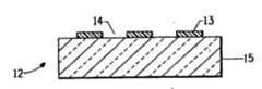
图1是具有形成微线路或其他功能性电子线路图案的浮雕结构的母模的剖视图。Figure 1 is a cross-sectional view of a master mold having a relief structure forming a microcircuit or other functional electronic circuit pattern.
图2是具有在载体和母模之间的弹性材料层的印刷形式前体的一个实施方式的剖视图,该弹性层将进行光化辐照曝光。Figure 2 is a cross-sectional view of one embodiment of a printing form precursor having a layer of elastomeric material between a support and a master tool to be exposed to actinic radiation.
图3是与母模分离的由印刷形式前体形成的压模的剖视图。该压模具有对应于母模浮雕图案的浮雕结构,具体地,压模的浮雕结构包括至少一个凸起表面和凹陷表面的图案,该图案与母模的浮雕图案相反。Figure 3 is a cross-sectional view of a stamper formed from a printing form precursor separated from a master mold. The stamper has a relief structure corresponding to the relief pattern of the master mold, in particular, the relief structure of the stamper comprises a pattern of at least one raised surface and recessed surface, which pattern is opposite to the relief pattern of the master mold.
图4是在压模的浮雕结构上施用掩模材料的实施方式中位于旋涂机平台上的弹性压模的剖面图。4 is a cross-sectional view of an elastomeric stamper on a spin coater platform in an embodiment in which a masking material is applied over a relief structure of the stamper.
图5是在与基材接触的浮雕结构的凸起表面上具有掩模材料层的弹性压模的剖面图。Figure 5 is a cross-sectional view of an elastomeric stamp with a layer of masking material on the raised surface of the relief structure in contact with the substrate.
图6是与基材分离并将凸起表面上的掩模材料转移至基材形成掩模材料图案的弹性压模的截面图。6 is a cross-sectional view of a resilient stamp detached from a substrate and transferring masking material on raised surfaces to the substrate to form a pattern of masking material.
图7是在基材上未被掩模材料图案覆盖的敞开区域施用功能材料的实施方式中在旋涂机平台上的具有掩模材料图案的基材的剖面图。7 is a cross-sectional view of a substrate with a pattern of masking material on a spin coater stage in an embodiment where a functional material is applied to open areas of the substrate not covered by the pattern of masking material.
图8是显示去除掩模材料在基材上形成功能材料的图案的实施方式中在一浴液中的具有功能材料的基材的剖面图。8 is a cross-sectional view of a substrate with functional material in a bath in an embodiment showing removal of masking material to form a pattern of functional material on the substrate.
图9是显示对功能材料进一步加热处理的任选步骤的实施方式中具有功能材料图案的基材的剖面图。9 is a cross-sectional view of a substrate having a pattern of a functional material in an embodiment showing an optional step of further heat-treating the functional material.
图10a是按照比较例中所述的方式制造的源漏线条的电子图案的图像。Figure 10a is an image of the electronic pattern of the source-drain lines fabricated in the manner described in Comparative Example.
图10b是按照实施例2中所述的方式制造的源漏线条的电子图案的图像。FIG. 10b is an image of the electronic pattern of source-drain lines fabricated as described in Example 2. FIG.
优选实施方式的详细描述Detailed description of the preferred embodiment
在下面的详细描述中,类似的附图标记表示所有附图中类似的要素。In the following detailed description, like reference numerals refer to like elements throughout the drawings.
本发明提供一种在用于电子应用的基材上形成功能材料的图案的方法。该方法可应用于形成作为功能材料的各种电子材料(包括导体、半导体和介电材料)的图案。该方法不限于使用硫醇材料作为掩模材料的弹性压模的应用。该方法能在各种大面积的基材上通常以至少1-5微米的线条分辨率形成功能材料的图案,因此特别能够形成微线路。该方法采用具有浮雕结构的弹性压模方便地印刷来转移掩模材料,压模没有发生下垂或明显的下垂以及没有发生不希望的至基材的材料转移。所述方法在功能材料的线条之间提供洁净的、敞开的无特征背景,同时保持与常规微接触印刷相关的图像逼真度和分辨率。该方法适合于电子器件和元件的高速制造工艺,如卷至卷工艺。The present invention provides a method of forming a pattern of a functional material on a substrate for electronic applications. The method can be applied to form patterns of various electronic materials including conductors, semiconductors and dielectric materials as functional materials. The method is not limited to the application of elastic stampers using thiol materials as mask materials. The method is capable of patterning functional materials on a variety of large area substrates, typically with a line resolution of at least 1-5 microns, and is therefore particularly capable of forming microcircuits. The method transfers masking material by printing conveniently with a resilient stamp having a relief structure without sagging or significant sagging of the stamp and without unwanted transfer of material to the substrate. The method provides a clean, open, featureless background between lines of functional material while maintaining the image fidelity and resolution associated with conventional microcontact printing. The method is suitable for high-speed manufacturing processes of electronic devices and components, such as roll-to-roll processes.
提供用于对基材图案化的压模。该压模包括具有凸起表面的浮雕结构。浮雕结构通常包括多个凸起表面和凹陷表面。压模的浮雕结构形成用以在基材上印刷掩模材料的凸起表面的图案。基材上的掩模材料的图案是电子元件或器件所需的功能材料图案的相反或负性的图案。即,弹性压模的浮雕结构的凹陷表面代表了将通过本方法在基材上最终形成的功能材料的图案,凸起表面代表了基材上无特征的背景区域。在一个实施方式中,本发明方法主要避免了因压模的浮雕表面结构而与标准微接触印刷相关的压模下垂的问题(即,凹陷部分中的顶部塌陷)。压模结构的凸起表面与凹陷表面宽度相比相对较宽。由于凹陷表面相对较窄的宽度尺寸,本发明形成并使用的弹性压模没有在凹陷表面发生下垂或明显下垂并且没有发生不希望的材料转移。压模自凸起表面印刷相对宽的掩模材料的线条,这些线条代表了最终形成的电子元件上的敞开的背景区域。在一个实施方式中,压模的浮雕结构具有凸起表面,凸起表面的宽度大于凹陷表面的宽度。虽然上述压模的浮雕结构的实施方式提供了特定益处,但本发明方法不仅仅限于凸起表面的宽度大于凹陷表面宽度的实施方式。所述方法可应用于形成功能材料的图案,而与压模凸起表面和凹陷表面的相对尺寸无关。A stamp for patterning a substrate is provided. The stamp includes a relief structure with a raised surface. Relief structures typically include a plurality of raised and recessed surfaces. The relief structure of the stamp forms a pattern of raised surfaces for printing a masking material on a substrate. The pattern of the masking material on the substrate is the inverse or negative pattern of the desired functional material pattern for the electronic component or device. That is, the concave surface of the relief structure of the elastic stamper represents the pattern of the functional material that will eventually be formed on the substrate by the method, and the convex surface represents the featureless background area on the substrate. In one embodiment, the inventive method substantially avoids the problem of stamper sagging (ie, top collapse in recessed portions) associated with standard microcontact printing due to the relief surface structure of the stamper. The convex surface of the stamper structure is relatively wide compared to the width of the concave surface. Due to the relatively narrow width dimension of the recessed surface, the present invention forms and uses a resilient stamper that does not sag or significantly sags at the recessed surface and does not experience unwanted material transfer. The stamper prints relatively wide lines of masking material from the raised surface that represent open background areas on the final formed electronic component. In one embodiment, the relief structure of the stamp has a raised surface, the width of which is greater than the width of the recessed surface. While the embodiments of the relief structure of the stamp described above provide certain benefits, the method of the present invention is not limited only to embodiments in which the width of the raised surface is greater than the width of the recessed surface. The method can be applied to form patterns of functional materials regardless of the relative dimensions of the raised and recessed surfaces of the stamper.
压模可以通过微接触印刷领域的技术人员理解的常规方式形成。例如,压模可以通过在具有呈现浮雕形式的表面(即与压模的浮雕结构相反)的母模上模塑并固化一层材料而制造。压模可以通过施加光化辐照、加热或它们的组合进行固化。因此压模包括一层弹性材料,该弹性材料层也称作弹性层、固化层或固化弹性层。压模例如还可以通过产生浮雕结构的方式对材料进行烧蚀或雕刻来制造。压模的浮雕结构能使得凸起表面具有自凹陷表面的高度,该高度足以使凸起表面与基材发生选择性的接触。在一个实施方式中,凸起表面自凹陷表面的高度约为0.2-20微米。在另一个实施方式中,凸起表面自凹陷表面的高度约为0.2-2微米。压模可以由任何能够通过浮雕印刷在基材上复制材料图案的材料制造。压模的材料为弹性的,以使压模的至少一个凸起部分顺应基材的表面,以促进掩模材料完全转移。聚合物材料适合形成弹性压模,聚合物材料包括但不限于,例如,硅聚合物,如聚二甲基硅氧烷(PDMS);环氧聚合物,共轭二烯烃的聚合物,包括聚异戊二烯、聚1,2-丁二烯、聚1,4-丁二烯和丁二烯/丙烯腈;A-B-A型嵌段共聚物的弹性体嵌段共聚物,其中,A代表非弹性嵌段,优选乙烯基聚合物,最优选聚苯乙烯,B代表弹性嵌段,优选聚丁二烯或聚异戊二烯;丙烯酸酯聚合物;以及氟聚合物。A-B-A嵌段共聚物的例子包括但不限于聚(苯乙烯-丁二烯-苯乙烯)和聚(苯乙烯-异戊二烯-苯乙烯)。聚合物材料可以是弹性体,或者可以在固化后成为弹性体。Stamps can be formed by conventional means understood by those skilled in the art of microcontact printing. For example, a stamper may be fabricated by molding and curing a layer of material over a master mold having a surface in relief (ie, as opposed to the relief structure of the stamper). The stamper can be cured by application of actinic radiation, heat, or a combination thereof. The stamper thus comprises a layer of elastic material, also called elastic layer, cured layer or cured elastic layer. The stamper can also be produced, for example, by ablation or engraving of the material in such a way that a relief structure is produced. The relief structure of the stamp enables the raised surface to have a height from the recessed surface sufficient to allow selective contact of the raised surface with the substrate. In one embodiment, the height of the raised surface from the recessed surface is about 0.2-20 microns. In another embodiment, the height of the raised surface from the recessed surface is about 0.2-2 microns. The stamper can be fabricated from any material capable of replicating a pattern of material on a substrate by relief printing. The material of the stamp is elastic such that at least one raised portion of the stamp conforms to the surface of the substrate to facilitate complete transfer of the masking material. Polymeric materials are suitable for forming elastic stampers and include, but are not limited to, for example, silicon polymers such as polydimethylsiloxane (PDMS); epoxy polymers, polymers of conjugated dienes, including poly Elastomeric block copolymers of isoprene, poly-1,2-butadiene, poly-1,4-butadiene and butadiene/acrylonitrile; A-B-A block copolymers, where A is non-elastomeric blocks, preferably vinyl polymers, most preferably polystyrene, B represents elastomeric blocks, preferably polybutadiene or polyisoprene; acrylate polymers; and fluoropolymers. Examples of A-B-A block copolymers include, but are not limited to, poly(styrene-butadiene-styrene) and poly(styrene-isoprene-styrene). The polymeric material may be elastomeric, or may become elastomeric after curing.
在一个实施方式中,形成弹性压模的材料是光敏性的,以使浮雕结构在暴露于光化辐照后而形成。术语“光敏的”包括其中的光敏组合物能够在感应光化辐照后引发一个或多个反应,特别是光化学反应的任何体系。在暴露于光化辐照后,通过缩合机理或通过自由基加成聚合引发单体和/或低聚物的链增长聚合。虽然设想了所有的光聚合机理,但是能用作弹性压模材料的光敏组合物可以按具有一个或多个烯键式不饱和端基的单体和/或低聚物的自由基引发的加成聚合内容进行描述。该内容中,在进行光化辐照曝光时,光引发剂体系可以用作引发单体和/或低聚物聚合反应所需的自由基源。In one embodiment, the material forming the elastic stamp is photosensitive such that the relief structure is formed upon exposure to actinic radiation. The term "photosensitive" includes any system in which the photosensitive composition is capable of initiating one or more reactions, especially photochemical reactions, in response to actinic radiation. Following exposure to actinic radiation, chain growth polymerization of monomers and/or oligomers is initiated by a condensation mechanism or by free radical addition polymerization. Although all mechanisms of photopolymerization are envisioned, photosensitive compositions useful as elastomeric stamping materials can be based on free-radical-initiated addition of monomers and/or oligomers having one or more ethylenically unsaturated end groups. into aggregated content for description. In this context, upon exposure to actinic radiation, the photoinitiator system can serve as a source of free radicals required to initiate polymerization of monomers and/or oligomers.
该组合物是光敏性的,因为组合物含有具有至少一个烯键式不饱和基团的化合物,所述烯键式不饱和基团能够通过光引发的加成聚合形成聚合物。该光敏组合物还包含通过光化辐照活化的引发体系,以引发光聚合。可聚合的化合物可具有非末端的烯键式不饱和基团,和/或该组合物可含有一种或多种其他组分,如能促进交联的单体。因此,术语“可光聚合的”用以涵盖可光聚合的体系,可光交联的体系,或者这两者。如本文所用,光聚合反应也指固化。形成弹性压模的光敏组合物包含一种或多种组分和/或添加剂,包括但不限于光引发剂,一种或多种烯键式不饱和化合物(可称作单体),填充料,表面活性剂,热聚合抑制剂,加工助剂,抗氧化剂,光敏剂等,以稳定或增强该组合物。The composition is photosensitive in that the composition contains a compound having at least one ethylenically unsaturated group capable of forming a polymer by photoinitiated addition polymerization. The photosensitive composition also comprises an initiating system activated by actinic radiation to initiate photopolymerization. The polymerizable compound may have non-terminal ethylenically unsaturated groups, and/or the composition may contain one or more other components, such as monomers that facilitate crosslinking. Thus, the term "photopolymerizable" is intended to encompass photopolymerizable systems, photocrosslinkable systems, or both. As used herein, photopolymerization also refers to curing. The photosensitive composition for forming an elastic stamper comprises one or more components and/or additives, including but not limited to photoinitiators, one or more ethylenically unsaturated compounds (which may be referred to as monomers), fillers , surfactants, thermal polymerization inhibitors, processing aids, antioxidants, photosensitizers, etc., to stabilize or enhance the composition.
光引发剂可以是对光化辐照敏感,产生引发聚合反应但不会导致过分终结反应的自由基的一种化合物或多种化合物的组合。可以使用任何已知类型的光引发剂,特别是自由基光引发剂,例如:芳族酮、醌、二苯甲酮、苯偶姻醚、芳基酮、过氧化物、双咪唑、苄基二甲基缩酮、羟烷基苯基苯乙酮、二烷氧基苯乙酮、三甲基苯甲酰氧化膦衍生物、氨基酮、苯甲酰环己醇、甲基苯硫基吗啉代酮、吗啉代苯基氨基酮、α-卤代苯乙酮、含氧磺酰酮、磺酰酮、含氧磺酰酮、磺酰酮、苯甲酰肟酯、硫代蒽酮(thioxanthrone)、樟脑醌、香豆素酮(ketocoumarin)和迈克尔酮(Michler’s ketone)。在一个实施方式中,光引发剂包括基于已知的芳族酮类的无氟光引发剂的氟化的光引发剂。或者,光引发剂可以是化合物的混合物,当通过辐射活化的感光剂致使混合物提供自由基时,由其中一种化合物提供自由基。液体光引发剂特别适合,因为液体光引发剂能很好分散在组合物中。较好地,引发剂对紫外线辐射敏感。以光敏组合物的重量为基准,光引发剂的存在量一般为0.001-10.0%。A photoinitiator may be a compound or a combination of compounds that is sensitive to actinic radiation and generates free radicals that initiate polymerization without causing excessive termination. Any known type of photoinitiator can be used, especially free radical photoinitiators such as: aromatic ketones, quinones, benzophenones, benzoin ethers, aryl ketones, peroxides, bis-imidazoles, benzyl Dimethyl ketal, hydroxyalkylphenylacetophenone, dialkoxyacetophenone, trimethylbenzoylphosphine oxide derivatives, aminoketone, benzoylcyclohexanol, methylphenylsulfanyl Linoxone, morpholinophenylaminoketone, α-halogenated acetophenone, oxygen-containing sulfonyl ketone, sulfonyl ketone, oxygen-containing sulfonyl ketone, sulfonyl ketone, benzoyl oxime ester, thioanthrone (thioxanthrone), camphorquinone, ketocoumarin and Michler's ketone. In one embodiment, the photoinitiator comprises a fluorinated photoinitiator based on known fluorine-free photoinitiators of aromatic ketones. Alternatively, the photoinitiator may be a mixture of compounds, one of which donates free radicals when the mixture is caused to donate by radiation-activated sensitizers. Liquid photoinitiators are particularly suitable because liquid photoinitiators disperse well in the composition. Preferably, the initiator is sensitive to ultraviolet radiation. The photoinitiator is generally present in an amount of 0.001-10.0% by weight of the photosensitive composition.
可用于能够通过光化辐照活化的组合物中的单体为本领域皆知,这类单体包括但不限于:加成聚合的烯键式不饱和化合物。加成聚合化合物也可以是低聚物,并可以是单一的低聚物或低聚物的混合物。组合物可含有单一单体或多种单体的组合。以组合物重量为基准,能进行加成聚合的单体化合物的存在量小于5%,优选小于3%。Monomers useful in compositions capable of being activated by actinic radiation are well known in the art and include, but are not limited to, addition polymerizable ethylenically unsaturated compounds. The addition polymeric compound may also be an oligomer, and may be a single oligomer or a mixture of oligomers. The composition may contain a single monomer or a combination of monomers. The addition polymerizable monomeric compound is present in an amount of less than 5%, preferably less than 3%, by weight of the composition.
在一个实施方式中,弹性压模由光敏组合物构成,该光敏组合物包含能在光化辐照曝光后聚合形成氟化的基于弹性体的材料的氟化化合物。合适的基于弹性体的氟化化合物包括但不限于:全氟聚醚、氟代烯烃,氟化热塑性弹性体,氟化环氧树脂,能通过聚合反应聚合或交联的氟化单体和氟化低聚物。一个实施方式中,氟化化合物具有一个或多个烯键式不饱和端基,这些端基能通过反应聚合形成氟化弹性体材料。基于弹性体的氟化化合物可以均聚,或与如以下聚合物共聚:聚氨酯,聚丙烯酸酯,聚酯,聚硅氧烷,聚酰胺和其他聚合物,以实现要求的印刷形式前体和/或适合其用途的压模的特性。进行光化辐照曝光足以使氟化化合物聚合,并使其能够用作印刷压模,而不必施加高压和/或高于室温的高温。含能通过光化辐照曝光固化的氟化化合物的组合物的优点是组合物能相对快速(如,在小于或等于1分钟内)固化,特别在与热固化组合物如基于PDMS的体系相比时,具有简单工艺过程方面的发展。In one embodiment, the elastomeric stamp is composed of a photosensitive composition comprising a fluorinated compound capable of polymerizing to form a fluorinated elastomer-based material upon exposure to actinic radiation. Suitable elastomer-based fluorinated compounds include, but are not limited to: perfluoropolyethers, fluoroolefins, fluorinated thermoplastic elastomers, fluorinated epoxies, fluorinated monomers that can be polymerized or crosslinked by polymerization, and fluorinated oligomers. In one embodiment, the fluorinated compound has one or more ethylenically unsaturated end groups capable of reaction polymerization to form a fluorinated elastomeric material. Elastomer-based fluorinated compounds can be homopolymerized, or copolymerized with polymers such as: polyurethanes, polyacrylates, polyesters, polysiloxanes, polyamides and other polymers to achieve the required printing form precursors and/or or the characteristics of a stamper suitable for its purpose. Exposure to actinic radiation is sufficient to polymerize the fluorinated compound and enable its use as a printing stamp without having to apply high pressure and/or elevated temperatures above room temperature. An advantage of compositions containing fluorinated compounds curable by exposure to actinic radiation is that the compositions cure relatively quickly (e.g., in less than or equal to 1 minute), especially when compared to thermally curable compositions such as PDMS-based systems. Compared with time, it has the development of simple process.
一个实施方式中,弹性压模包括一层光敏组合物,其中,氟化化合物是全氟聚醚(PFPE)化合物。全氟聚醚化合物是包含至少大比例全氟醚链段的化合物,即全氟聚醚。以PFPE化合物的总重量为基准,在PFPE化合物中存在的大比例全氟醚链段大于或等于80重量%。全氟聚醚化合物还可包含一种或多种增量链段,这些链段是非氟化的烃或烃醚;和/或是氟化但非全氟化的烃或烃醚。一个实施方式中,全氟聚醚化合物包含至少大比例的全氟聚醚链段和光反应性的端链段,以及任选的非氟化烃的增量链段。全氟聚醚化合物是以一个或多个烯键式不饱和端基官能化,所述烯键式不饱和端基使该化合物对光化辐照为反应活性(即,光反应性链段)。光反应性链段也称作可光聚合的链段。In one embodiment, the elastomeric stamper comprises a layer of a photosensitive composition, wherein the fluorinated compound is a perfluoropolyether (PFPE) compound. A perfluoropolyether compound is a compound comprising at least a large proportion of perfluoroether segments, ie a perfluoropolyether. Based on the total weight of the PFPE compound, the large proportion of perfluoroether chain segments present in the PFPE compound is greater than or equal to 80% by weight. The perfluoropolyether compound may also comprise one or more extender segments that are non-fluorinated hydrocarbons or hydrocarbon ethers; and/or fluorinated but not perfluorinated hydrocarbons or hydrocarbon ethers. In one embodiment, the perfluoropolyether compound comprises at least a major proportion of perfluoropolyether segments and photoreactive end segments, and optionally non-fluorinated hydrocarbon extender segments. Perfluoropolyether compounds are functionalized with one or more ethylenically unsaturated end groups that render the compound reactive to actinic radiation (i.e., photoreactive segments) . Photoreactive segments are also referred to as photopolymerizable segments.
对全氟聚醚化合物没有限制,可以包含直链和支链结构,优选全氟聚醚化合物的直链主链结构。PFPE化合物可以是单体的,但通常是低聚物,并在室温为液体。全氟聚醚化合物可以被认为是具有低聚全氟醚链段的低聚的双官能单体。全氟聚醚化合物能光化学聚合形成压模的弹性体层。基于PFPE的材料的优点是,PFPE是高度氟化的,能耐受有机溶剂溶胀,所述有机溶剂例如有,二氯甲烷,氯仿,四氢呋喃,甲苯,己烷和乙腈等,优选将这些有机溶剂用于微接触印刷技术。The perfluoropolyether compound is not limited, and may contain linear and branched structures, preferably a linear main chain structure of the perfluoropolyether compound. PFPE compounds can be monomeric, but are usually oligomeric and liquid at room temperature. Perfluoropolyether compounds can be considered as oligomeric difunctional monomers having oligomeric perfluoroether segments. The perfluoropolyether compound can be photochemically polymerized to form the elastomeric layer of the stamper. The advantage of PFPE-based materials is that PFPE is highly fluorinated and resistant to swelling with organic solvents such as dichloromethane, chloroform, tetrahydrofuran, toluene, hexane and acetonitrile, etc., preferably these organic solvents For microcontact printing techniques.
任选地,弹性压模可包括挠性膜载体,优选挠性聚合物膜。挠性载体能够使压模的弹性浮雕表面顺应或基本顺应于可印刷的电子基板,不会发生翘曲或变形。载体也是充分挠性的,能够在从母模剥离压模时与弹性体层一起弯曲。载体可以是能形成膜的任何聚合物材料,所述膜是非反应性的,并在制造和使用压模期间的所有状况下保持稳定。合适的膜载体的例子包括纤维素膜,如,三乙酰基纤维素;和热塑性材料如聚烯烃,聚碳酸酯,聚酰亚胺和聚酯。优选聚乙烯膜,如聚对苯二甲酸乙二酯和聚萘二甲酸乙二酯。载体也包括挠性玻璃。通常,载体的厚度为2-50密耳(0.0051-0.13厘米)。通常,载体为片形,但不限于片形。在一个实施方式中,载体能透过或基本透过使光敏组合物聚合的光化辐射。Optionally, the elastic stamp may comprise a flexible film support, preferably a flexible polymeric film. The flexible carrier enables the elastic relief surface of the stamp to conform or substantially conform to the printable electronic substrate without warping or deformation. The carrier is also sufficiently flexible to bend with the elastomeric layer when the stamp is released from the master tool. The support may be any polymeric material capable of forming a film which is non-reactive and stable under all conditions during manufacture and use of the stamper. Examples of suitable film supports include cellulosic films, eg, triacetyl cellulose; and thermoplastic materials such as polyolefins, polycarbonates, polyimides and polyesters. Polyethylene films such as polyethylene terephthalate and polyethylene naphthalate are preferred. The carrier also includes flexible glass. Typically, the thickness of the support is 2-50 mils (0.0051-0.13 centimeters). Usually, the carrier is in the shape of a sheet, but not limited to a sheet. In one embodiment, the carrier is transparent or substantially transparent to actinic radiation that polymerizes the photosensitive composition.
任选地,弹性压模在施加掩模材料之前可在浮雕表面上包括一个或多个层。所述一个或多个层例如可帮助掩模材料从压模转移至基材。适合用作附加层的材料的例子包括氟化化合物。在一个实施方式中,在掩模材料转移至基材后附加层仍保留在弹性压模上。Optionally, the elastomeric stamper may include one or more layers on the relief surface prior to application of the masking material. The one or more layers may, for example, aid in the transfer of masking material from the stamp to the substrate. Examples of materials suitable for use as additional layers include fluorinated compounds. In one embodiment, the additional layer remains on the elastomeric stamp after the mask material is transferred to the substrate.
通过将掩模材料至少施加至压模的浮雕结构的凸起表面,可向压模提供掩模材料。可以通过任意合适方法将掩模材料施加至压模,这些方法包括但不限于,注射、灌注、液体浇铸、喷射、浸渍、喷雾、气相沉积以及涂覆。进行涂覆的适当方法的例子包括旋涂,浸涂,缝式涂布,辊涂,刮刀刮涂。一个实施方式中,将掩模材料施加至压模的浮雕结构,即,掩模材料在凸起表面和凹陷表面上形成一个层。压模上的掩模材料层可以是连续的或不连续的。对掩模材料层的厚度没有特别的限制,只要该材料能够印刷并在基材上起到掩模的作用即可。一个实施方式中,掩模材料层的厚度通常小于压模的浮雕高度(为凸起表面和凹陷表面之间的差)。在一个实施方式中,压模上掩模材料层为0.01-1微米。The stamper may be provided with a masking material by applying the masking material to at least the raised surface of the relief structure of the stamper. The masking material may be applied to the stamp by any suitable method including, but not limited to, injection, pouring, liquid casting, jetting, dipping, spraying, vapor deposition, and coating. Examples of suitable methods of applying the coating include spin coating, dip coating, slot coating, roll coating, doctor blade coating. In one embodiment, the masking material is applied to the relief structure of the stamp, ie the masking material forms one layer on the raised and recessed surfaces. The layer of masking material on the stamp can be continuous or discontinuous. There is no particular limitation on the thickness of the mask material layer, as long as the material can be printed and function as a mask on the substrate. In one embodiment, the thickness of the layer of masking material is generally less than the relief height (the difference between the raised surface and the recessed surface) of the stamper. In one embodiment, the mask material layer on the stamper is 0.01-1 micron.
至少在压模的凸起表面施加掩模材料后,掩模材料可以任选干燥,以除去部分或所有的载剂或溶剂,然后转移到基材上。可以任意方式实现干燥,干燥方式包括:使用气体射流,用吸收材料吸干,室温或升高温度下蒸发等。一个实施方式中,掩模材料基本上不含溶剂或载剂,然后转移,在凸起表面上形成膜。After applying the masking material to at least the raised surface of the stamp, the masking material can optionally be dried to remove some or all of the vehicle or solvent, and then transferred to the substrate. Drying may be achieved in any manner including: use of a gas jet, blotting with absorbent material, evaporation at room or elevated temperature, and the like. In one embodiment, the masking material is substantially free of solvent or vehicle and then transferred to form a film on the raised surface.
掩模材料的选择由最终图案化的功能材料决定。掩模材料通常分散或溶解或悬浮于溶液中,以施用于压模。功能材料通常也分散或溶解或悬浮于溶液中,以施用于基材。无论功能材料是有机化合物或水基化合物或醇基化合物,用于功能材料的溶液的类型决定了掩模材料以及相应分散或溶解或悬浮该掩模材料的溶液。掩模材料不应使用与功能材料使用的相同或基本上相同或类似的溶液。该溶液可以是溶剂,即能溶解另一种物质形成均匀分散的混合物的物质,或者是载剂化合物,这种化合物能将材料分散或悬浮于溶液中,分散或悬浮的程度足以进行本发明方法的步骤。The choice of mask material is determined by the final patterned functional material. Masking materials are typically dispersed or dissolved or suspended in solution for application to the stamp. Functional materials are also typically dispersed or dissolved or suspended in solution for application to the substrate. Whether the functional material is an organic compound or a water-based compound or an alcohol-based compound, the type of solution used for the functional material determines the mask material and the corresponding solution to disperse or dissolve or suspend the mask material. Masking materials should not use the same or substantially the same or similar solutions as those used for functional materials. The solution may be a solvent, i.e. a substance capable of dissolving another substance to form a uniformly dispersed mixture, or a carrier compound capable of dispersing or suspending a material in solution to an extent sufficient to carry out the process of the invention A step of.
特定的实施方式中,掩模材料的溶液与功能材料的溶液不相容或基本不相容。即,在一个实施方式中,如果功能材料存在于含有有机化合物的溶液中,则选择掩模材料与有机溶液不相容或基本不相容,(即,掩模材料分散或溶解或悬浮于水溶液或醇溶液中)。在一个实施方式中,如果功能材料存在于含有水性化合物或醇化合物的溶液中,则选择掩模材料与水溶液或醇溶液不相容或基本不相容,(即,掩模材料分散或溶解或悬浮于有机溶液中)。一个实施方式中,掩模材料和功能材料是不相容或基本不相容的,使得在将功能材料施加到基材上的掩模材料图案上时,功能材料不会或基本上不会改变或破坏或者影响掩模材料的图案。在另一个实施方式中,掩模材料和功能材料不相容或基本不相容,使得功能材料和掩模材料彼此相邻时不会混合或溶解。在另一个实施方式中,掩模材料和功能材料不相容或基本不相容,使得通过溶剂溶液除去掩模材料(在施加功能材料后)不会破坏功能材料在基材上形成图案。改变或破坏图案的例子包括溶解或溶胀掩模材料以及从基材剥离(lifting)掩模材料(当与功能材料接触时);以及溶解或溶胀功能材料以及从基材上剥离功能材料(特别是当从基材上除去掩模材料时)。还预期在本发明方法范围内,掩模材料和功能材料都使用相同的一般性溶液,即,都使用有机溶液,或都使用醇溶液,但仍是不相容或基本不相容的。在这种情况,只要掩模材料溶液的溶解度和功能材料溶液的溶解度之间的差异足以在施用功能材料时不会对基材上的掩模材料图案产生不利影响,并且在去除掩模材料时不会对形成功能材料图案产生不利影响,就可以认为掩模材料和功能材料是基本不相容的(参见实施例1和3)。In particular embodiments, the solution of the masking material is incompatible or substantially incompatible with the solution of the functional material. That is, in one embodiment, if the functional material is present in a solution containing an organic compound, the masking material is selected to be incompatible or substantially incompatible with the organic solution, (i.e., the masking material is dispersed or dissolved or suspended in an aqueous solution or alcohol solution). In one embodiment, if the functional material is present in a solution containing an aqueous compound or an alcoholic compound, the masking material is selected to be incompatible or substantially incompatible with the aqueous or alcoholic solution, (i.e., the masking material disperses or dissolves or suspended in an organic solution). In one embodiment, the masking material and the functional material are incompatible or substantially incompatible such that the functional material does not or substantially does not change when the functional material is applied to the pattern of the masking material on the substrate Either destroy or affect the pattern of the mask material. In another embodiment, the masking material and the functional material are incompatible or substantially incompatible such that the functional material and the masking material do not mix or dissolve when adjacent to each other. In another embodiment, the masking material and the functional material are incompatible or substantially incompatible such that removal of the masking material (after application of the functional material) by a solvent solution does not disrupt the patterning of the functional material on the substrate. Examples of changing or disrupting patterns include dissolving or swelling the mask material and lifting the mask material from the substrate (when in contact with the functional material); and dissolving or swelling the functional material and lifting the functional material from the substrate (especially when removing the masking material from the substrate). It is also contemplated within the scope of the method of the present invention that both the masking material and the functional material use the same general solution, ie both use an organic solution, or both use an alcoholic solution, but are still incompatible or substantially incompatible. In this case, as long as the difference between the solubility of the masking material solution and the solubility of the functional material solution is sufficient to not adversely affect the pattern of the masking material on the substrate when the functional material is applied, and when the masking material is removed The mask material and the functional material can be considered substantially incompatible without adversely affecting the patterning of the functional material (see Examples 1 and 3).
掩模材料应具有以下性能:(1)能够至少在压模浮雕结构的凸起表面上形成一个层;(2)能够将依据浮雕结构的图案转移至基材;和(3)能够从基材上去除而不会对功能材料产生不利影响(不会影响如果存在的下层)。弹性压模的一些性质可能影响特定掩模材料形成层并转移至基材的能力,但是微接触印刷领域的技术人员能够决定掩模材料和弹性压模的适当组合。在一个实施方式中,掩模材料还能够使功能材料覆盖全部或部分的掩模图案。The mask material should have the following properties: (1) capable of forming a layer at least on the raised surface of the stamp relief structure; (2) capable of transferring the pattern according to the relief structure to the substrate; removal without adversely affecting the functional material (and without affecting the underlying layer, if present). Some properties of the elastomeric stamp may affect the ability of a particular masking material to form a layer and transfer to a substrate, but one skilled in the art of microcontact printing will be able to determine the appropriate combination of masking material and elastomeric stamper. In one embodiment, the mask material can also allow the functional material to cover all or part of the mask pattern.
对适合用作掩模材料的材料没有特别的限制,只要掩模材料能满足上述要求即可。适合用作对在水性溶液或水溶液中的功能材料的掩模的材料的例子包括但不限于:丙烯腈均聚物和共聚物,如丙烯腈-丁二烯弹性体,和聚(丙烯腈);苯乙烯均聚物和共聚物,如聚苯乙烯和聚(苯乙烯-丙烯腈)共聚物;丙烯酸酯和甲基丙烯酸酯的均聚物和共聚物,如聚丙烯酸酯、聚(甲基丙烯酸乙酯),和聚甲基丙烯酸酯;聚碳酸酯;聚氨酯;聚噻吩;取代和未取代的聚亚苯基-亚乙烯基均聚物和共聚物;聚(4-乙烯基吡啶);聚(异氰酸正己酯);聚(1,4-亚苯基亚乙烯基);基于环氧化物的体系;聚(正咔唑);聚降冰片烯的均聚物和共聚物;聚(苯醚);聚(苯硫醚);聚(四氟乙烯);以及它们的共聚物和组合。There is no particular limitation on materials suitable for use as a mask material, as long as the mask material can satisfy the above-mentioned requirements. Examples of materials suitable for use as masks for functional materials in aqueous solutions or aqueous solutions include, but are not limited to: acrylonitrile homopolymers and copolymers, such as acrylonitrile-butadiene elastomers, and poly(acrylonitrile); Homopolymers and copolymers of styrene, such as polystyrene and poly(styrene-acrylonitrile) copolymers; homopolymers and copolymers of acrylates and methacrylates, such as polyacrylates, poly(methacrylic acid) ethyl ester), and polymethacrylates; polycarbonates; polyurethanes; polythiophenes; substituted and unsubstituted polyphenylene-vinylene homopolymers and copolymers; poly(4-vinylpyridine); poly (n-hexylisocyanate); poly(1,4-phenylene vinylene); epoxy-based systems; poly(n-carbazole); homopolymers and copolymers of polynorbornene; poly( phenylene ether); poly(phenylene sulfide); poly(tetrafluoroethylene); and copolymers and combinations thereof.
适合用作对在有机溶液中的功能材料的掩模的材料的例子包括但不限于:醇酸树脂;明胶;聚(丙烯酸);多肽;蛋白质;聚(乙烯基吡啶);聚(乙烯基吡咯烷酮);羟基聚苯乙烯;聚(乙烯醇);聚乙二醇;脱乙酰壳多糖;(苯乙烯-乙烯基吡啶)共聚物;(丙烯酸丁酯-乙烯基吡啶)共聚物;芳基胺和氟化的芳基胺;纤维素和纤维素衍生物;丙烯酸酯和/或甲基丙烯酸酯乳液的分散体;以及它们的共聚物和组合。Examples of materials suitable for use as masks for functional materials in organic solutions include, but are not limited to: alkyd resins; gelatin; poly(acrylic acid); polypeptides; proteins; poly(vinylpyridine); poly(vinylpyrrolidone) ; hydroxypolystyrene; poly(vinyl alcohol); polyethylene glycol; chitosan; (styrene-vinylpyridine) copolymer; (butyl acrylate-vinylpyridine) copolymer; arylamine and fluorine arylamines; cellulose and cellulose derivatives; dispersions of acrylate and/or methacrylate emulsions; and copolymers and combinations thereof.
将掩模材料从浮雕结构的凸起表面转移至基材的步骤在基材上形成掩模材料的图案并相应在基材上形成敞开区域图案。转移也可称作印刷。使凸起表面上的掩模材料与基材接触的步骤将掩模材料转移,从而在将压模与基材分离时形成掩模材料的图案。一个实施方式中,凸起表面上的所有或基本上所有掩模材料都转移至基材。可通过任意合适的方式将压模与基材分离,这些方式包括但不限于:剥离,气体喷射,液体喷射,机械装置等。任选地,可以在压模上施加压力以保证掩模材料与基材的接触并完全转移至基材。可以以任意方式实现将掩模材料转移至基材。转移掩模材料可以通过将压模的浮雕表面移至基材,或者通过将基材移至压模的浮雕表面,或者通过同时移动基材和浮雕表面使它们接触而实现。一个实施方式中,掩模材料可以用手进行转移。在另一个实施方式中,自动化进行掩模材料的转移,例如通过传输带;卷至卷工艺;直接驱动移动固定装置或托盘;链条、带或齿轮-驱动的固定装置或托盘;摩擦辊;印刷压机;或旋转装置。The step of transferring the masking material from the raised surface of the relief structure to the substrate forms a pattern of the masking material on the substrate and a corresponding pattern of open areas on the substrate. Transfer may also be referred to as printing. The step of contacting the masking material on the raised surface with the substrate transfers the masking material to form a pattern of the masking material when the stamp is separated from the substrate. In one embodiment, all or substantially all of the masking material on the raised surface is transferred to the substrate. The stamper can be separated from the substrate by any suitable means including, but not limited to, peeling, gas jets, liquid jets, mechanical means, and the like. Optionally, pressure can be applied to the stamp to ensure contact and complete transfer of the masking material to the substrate. Transfer of the masking material to the substrate can be accomplished in any manner. Transfer of the mask material can be accomplished by moving the relief surface of the stamp to the substrate, or by moving the substrate to the relief surface of the stamp, or by simultaneously moving the substrate and relief surface into contact. In one embodiment, the mask material can be transferred by hand. In another embodiment, mask material transfer is automated, such as by conveyor belts; roll-to-roll process; direct-drive moving fixtures or trays; chain, belt, or gear-driven fixtures or trays; friction rollers; printing presses; or rotary devices.
对掩模材料层的厚度没有特别的限制,基材上的掩模材料层的厚度通常为100-
对基材没有限制,基材可包括:塑料、聚合物膜、金属、硅、玻璃、织品、纸以及它们的组合,只要可以在其上形成掩模图案即可。所述基材可以是不透明的或透明的。所述基材可以是刚性的或挠性的。在基材上形成依据本发明方法的功能材料的图案之前,基材可包括其他材料的一个或多个层和/或一个或多个图案。基材表面可包含增粘表面如底涂层,或者可以进行处理以促进粘合剂层或掩模材料或功能材料与基材的粘合。合适的基材包括,例如,聚合物、玻璃或陶瓷基材上的金属膜,在聚合物基材上的一层或多层导电膜上的金属膜,在聚合物基材上的半导体膜上的金属膜。合适基材的进一步的例子包括,例如,玻璃,氧化铟锡涂覆的玻璃,氧化铟锡涂覆的聚合物膜;聚对苯二甲酸乙二酯,聚萘二甲酸乙二酯,聚酰亚胺,硅和金属箔。There is no limitation on the substrate, and the substrate may include: plastic, polymer film, metal, silicon, glass, fabric, paper, and combinations thereof, as long as a mask pattern can be formed thereon. The substrate can be opaque or transparent. The substrate can be rigid or flexible. The substrate may comprise one or more layers and/or one or more patterns of other materials prior to forming a pattern of functional material on the substrate according to the method of the present invention. The substrate surface may comprise an adhesion promoting surface such as a primer, or may be treated to promote adhesion of an adhesive layer or masking material or functional material to the substrate. Suitable substrates include, for example, metallic films on polymeric, glass or ceramic substrates, metallic films on one or more conductive films on polymeric substrates, semiconductive films on polymeric substrates metal film. Further examples of suitable substrates include, for example, glass, indium tin oxide-coated glass, indium tin oxide-coated polymer films; polyethylene terephthalate, polyethylene naphthalate, polyamide imine, silicon and metal foils.
在基材上形成掩模材料的图案后,至少将功能材料施用于基材上掩模图案之间的一个或多个敞开区域中。一个实施方式中,施用功能材料以覆盖基材的表面,即,覆盖掩模图案和基材上的敞开区域。在另一个实施方式中,选择性施用功能材料以至少覆盖基材上的一个或多个敞开区域(基材上没有掩模材料的图案的区域)。选择性施用功能材料可以通过例如喷射进行。可以通过任意合适方法将功能材料施用至基材,这些方法包括但不限于,注射、灌注、液体浇铸、喷射、浸渍、喷雾、气相沉积以及涂覆。进行涂覆的适当方法的例子包括旋涂,浸涂,缝式涂布,辊涂,刮刀刮涂。After forming the pattern of masking material on the substrate, at least the functional material is applied to the substrate in one or more open areas between the masking patterns. In one embodiment, the functional material is applied to cover the surface of the substrate, ie to cover the mask pattern and open areas on the substrate. In another embodiment, the functional material is selectively applied to cover at least one or more open areas (areas of the substrate free of the pattern of masking material) on the substrate. The selective application of functional materials can be carried out, for example, by spraying. The functional material can be applied to the substrate by any suitable method including, but not limited to, injection, pouring, liquid casting, spraying, dipping, spraying, vapor deposition, and coating. Examples of suitable methods of applying the coating include spin coating, dip coating, slot coating, roll coating, doctor blade coating.
在基材上施用功能材料之后,可使功能材料干燥,以去除部分或全部的载剂或溶剂,然后从基材上去除掩模图案。可以任意方式实现干燥,干燥方式包括:使用气体射流,用吸收材料吸干,室温或升高温度下蒸发等。一个实施方式中,功能材料基本上不含溶剂或载剂,然后在基材的表面上形成膜。After applying the functional material on the substrate, the functional material may be dried to remove part or all of the vehicle or solvent, and then the mask pattern is removed from the substrate. Drying may be achieved in any manner including: use of a gas jet, blotting with absorbent material, evaporation at room or elevated temperature, and the like. In one embodiment, the functional material is substantially free of solvent or vehicle and then forms a film on the surface of the substrate.
功能材料是能图案化用于微制造电子元件和器件的材料。功能材料包括但不限于,例如,导体材料,半导体材料,介电材料等。用作功能材料的导体材料的例子包括但不限于:氧化铟锡;金属,如银、金、铜和钯;金属配合物;金属合金等。半导体材料的例子包括但是不限于:硅,锗,砷化镓,氧化锌和硒化锌。Functional materials are materials that can be patterned for microfabrication of electronic components and devices. Functional materials include, but are not limited to, for example, conductive materials, semiconductor materials, dielectric materials, and the like. Examples of conductor materials used as functional materials include, but are not limited to: indium tin oxide; metals such as silver, gold, copper, and palladium; metal complexes; metal alloys, and the like. Examples of semiconductor materials include, but are not limited to: silicon, germanium, gallium arsenide, zinc oxide, and zinc selenide.
功能材料可以是任意形式,包括微粒、聚合物、分子等。通常,半导体材料和介电材料是聚合物,但是不限于这种形式,功能材料可以包括可溶性的半导体分子。Functional materials can be in any form, including particles, polymers, molecules, etc. Typically, semiconducting and dielectric materials are polymers, but not limited to this form, functional materials may include soluble semiconducting molecules.
用于本发明方法的功能材料还包括导体、半导体和介电材料的纳米颗粒。纳米颗粒是显微颗粒,其测定的尺寸为纳米(nm)级。纳米颗粒包括至少一个尺寸小于200纳米的颗粒。一个实施方式中,纳米颗粒的直径约为3-100纳米。在粒度范围的下限,纳米颗粒可称作簇(cluster)。对纳米颗粒的形状没有限制,包括纳米球、纳米棒和纳米杯。如果颗粒小(通常小于10纳米)到足以发生电子能级的量子化,则由半导体材料构成的纳米颗粒也称作量子点(quantum dot)。半导体材料包括发光量子点。大块材料一般具有稳定的物理性质,而与其尺寸无关,但是对纳米颗粒一般不再是这种情况。观察到与尺寸相关的性质,例如半导体颗粒中的量子束缚,某些金属颗粒中的表面等离子体激元共振(surface plasmon resonance)以及磁性材料中的超顺磁性。功能材料包括但不限于半固体的纳米颗粒,例如脂质体;软的纳米颗粒;纳米晶体;杂化结构,如芯-壳纳米颗粒。功能材料包括碳纳米颗粒,如碳纳米管,导电碳纳米管和半导体碳纳米管。金、银和铜的金属纳米颗粒和分散体可从纳米技术(Nanotechnologies)和ANP获得。Functional materials useful in the method of the invention also include nanoparticles of conductive, semiconducting and dielectric materials. Nanoparticles are microscopic particles whose dimensions are measured on the nanometer (nm) scale. Nanoparticles include particles having at least one dimension less than 200 nanometers. In one embodiment, the nanoparticles are about 3-100 nanometers in diameter. At the lower end of the particle size range, nanoparticles may be referred to as clusters. There is no limitation on the shape of the nanoparticles, including nanospheres, nanorods, and nanocups. Nanoparticles composed of semiconductor materials are also called quantum dots if the particles are small enough (typically less than 10 nanometers) to quantize electronic energy levels. Semiconductor materials include light-emitting quantum dots. Bulk materials generally have stable physical properties independent of their size, but this is generally no longer the case for nanoparticles. Size-dependent properties have been observed, such as quantum confinement in semiconductor particles, surface plasmon resonance in certain metallic particles, and superparamagnetism in magnetic materials. Functional materials include, but are not limited to, semi-solid nanoparticles, such as liposomes; soft nanoparticles; nanocrystals; hybrid structures, such as core-shell nanoparticles. Functional materials include carbon nanoparticles such as carbon nanotubes, conductive carbon nanotubes and semiconducting carbon nanotubes. Metal nanoparticles and dispersions of gold, silver and copper are available from Nanotechnologies and ANP.
一个实施方式中,功能材料以溶液形式施用于基材。另一个实施方式中,功能材料为液体而不必以溶液形式施用于基材。特别在功能材料为纳米颗粒形式时,将功能材料悬浮于载剂体系中。如上面实施方式中所述,用于功能材料的溶剂或载剂体系应与转移至基材的掩模材料不相容或基本不相容。另一个实施方式中,功能材料至少与随后用于除去掩模材料的溶剂溶液不相容或基本不相容。In one embodiment, the functional material is applied to the substrate in solution. In another embodiment, the functional material is a liquid and need not be applied to the substrate in solution. Especially when the functional material is in the form of nanoparticles, the functional material is suspended in the carrier system. As mentioned in the above embodiments, the solvent or vehicle system used for the functional material should be incompatible or substantially incompatible with the masking material transferred to the substrate. In another embodiment, the functional material is at least incompatible or substantially incompatible with the solvent solution subsequently used to remove the masking material.
将功能材料施用于基材并形成膜之后,从该基材去除掩模图案。去除掩模材料图案可通过任何方法实施,这些方法包括但不限于:用溶剂溶液浸渍或润湿,和施加激光辐照。对基材上的掩模材料施加激光辐照不限于任何以去除掩模图案的具体机理,去除掩模图案的机理包括但不限于:烧蚀除去基材的掩模材料,通过溶胀、剥离或转移掩模材料改变掩模材料与基材的粘合性平衡。一个实施方式中,掩模材料的图案通过以下方式从基材上去除,将基材浸在用于掩模材料的溶剂浴中保持足够的时间,以使掩模图案与基材分离。通过溶剂进行去除可能引起掩模图案全部或部分发生剥离,溶胀,溶解,分散到溶剂溶液中,或这些现象的组合。任选地,掩模材料的去除可借助于声波处理,即对溶剂溶液施加强烈的声波。声波处理也称作声波清洁。一个实施方式中,覆盖全部或部分掩模材料图案的功能材料也可以和掩模材料同时去除。另一个实施方式中,去除覆盖掩模图案的功能材料与去除掩模材料分开单独进行。掩模材料的去除不应破坏或影响与基材(或与并非掩模材料的下层)接触的功能材料。如果在基材的掩模图案和敞开区域上都施用功能材料形成的层,则除去掩模图案(和上层功能材料)导致在基材上形成功能材料的图案。After applying the functional material to the substrate and forming a film, the mask pattern is removed from the substrate. Removing the pattern of masking material may be performed by any method including, but not limited to, dipping or wetting with a solvent solution, and application of laser radiation. Applying laser radiation to the masking material on the substrate is not limited to any particular mechanism for removing the masking pattern, which includes, but is not limited to: ablative removal of the masking material from the substrate, removal of the masking material by swelling, lift-off, or Transferring the mask material changes the adhesive balance of the mask material to the substrate. In one embodiment, the pattern of masking material is removed from the substrate by immersing the substrate in a solvent bath for the masking material for a sufficient time to separate the masking pattern from the substrate. Removal by a solvent may cause all or part of the mask pattern to lift off, swell, dissolve, disperse into the solvent solution, or a combination of these phenomena. Optionally, the removal of the masking material can be by means of sonication, ie applying intense sound waves to the solvent solution. Sonication is also known as sonic cleaning. In one embodiment, the functional material covering all or part of the pattern of the mask material can also be removed simultaneously with the mask material. In another embodiment, removing the functional material covering the mask pattern is performed separately from removing the mask material. Removal of the masking material should not destroy or affect the functional material in contact with the substrate (or with an underlying layer that is not the masking material). If a layer of functional material is applied over both the mask pattern and the open areas of the substrate, removal of the mask pattern (and overlying functional material) results in the formation of a pattern of functional material on the substrate.
虽然本发明方法可用来形成电子器件或元件的任意图案层,但是该方法特别适合用于形成功能材料的初始图案。在具有一个以上位于施用的功能材料之下的附加层的基材中,必须小心选择溶剂溶液,以除去掩模材料,使得下层没有因为与用于掩模材料的溶剂接触而受到影响或破坏。_Although the method of the present invention can be used to form any patterned layer of an electronic device or component, the method is particularly suitable for forming an initial pattern of a functional material. In substrates with more than one additional layer underlying the applied functional material, the solvent solution must be carefully selected to remove the masking material such that the underlying layer is not affected or destroyed by contact with the solvent used for the masking material. _
任选地,可以对具有功能材料的图案的基材进行进一步的处理步骤,例如,加热,施加光化辐照源,如紫外辐照和红外辐照等。所述处理步骤可以在去除步骤之后或恰在去除步骤之前进行。在功能材料为纳米颗粒形式的实施方式中,附加的处理步骤是使功能材料具备可操作性所必需的。例如,当功能材料由金属纳米颗粒构成时,必须加热功能材料的图案以烧结颗粒并使图案线条具备导电性。Optionally, the substrate with the pattern of functional material may be subjected to further processing steps, eg, heating, application of sources of actinic radiation, such as ultraviolet and infrared radiation, and the like. The treatment step can be performed after the removal step or just before the removal step. In embodiments where the functional material is in the form of nanoparticles, additional processing steps are necessary to render the functional material operable. For example, when the functional material is composed of metal nanoparticles, the pattern of functional material must be heated to sinter the particles and render the patterned lines conductive.
参见图1至图3,由压模前体10制造压模5的方法的实施方式按成型操作进行。图1示出母模12,该母模具有形成在母模基材15的表面14上的微电子特征的负片浮雕图案13。母模基材15可以是任何光滑或基本光滑的金属,塑料,陶瓷或玻璃。一个实施方式中,母模基板是玻璃板或硅板。按照本领域技术人员皆知的常规方法,通常由光刻胶材料形成在母模基材15上的浮雕图案13。也可以使用塑料接枝膜(grating film)和石英接枝膜作为母模。如果需要纳米规格的非常微小的特征元件,则可以采用电子束辐射在硅晶片上形成母模。Referring to Figures 1 to 3, an embodiment of a method of manufacturing a
可以将母模12放置在模具外壳和/或与隔板(未示出)一起沿其周边放置,以帮助形成均匀的光敏组合物层。形成压模的工艺通过不使用模具外壳或隔板而得到简化。
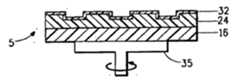
在图2所示的一个实施方式中,引入光敏组合物,在具有浮雕图案13的母模12的表面上形成层20。可以采用任何合适的方法将光敏组合物引入在母模12上,所述方法包括但不限于,注射,灌注,液体浇铸和涂覆。一个实施方式中,通过将光敏组合物的液体灌注在母模上,形成层20。在母模12上形成光敏组合物的层20,使得进行光化辐射曝光后,固化的组合物形成约5-50微米厚度的固体弹性体层。将载体16设置在光敏组合物层20与母模12相反的一面上,如果有粘合剂层时使该层与光敏组合物层相邻,形成压模前体10。可以适合获得压模前体10的任意方式,将载体16施加在组合物层上。在通过压模前体10的透明载体16施加光化辐照后(在所示的实施方式中是紫外辐照),光敏层20聚合并形成用于压模5的组合物的弹性体层24。光敏组合物层20通过光化辐照曝光进行固化或聚合。此外,通常在氮气氛中进行曝光,以消除或减少曝光期间环境中氧的存在,以及氧可以对聚合反应产生的影响。In one embodiment shown in FIG. 2 , a photosensitive composition is introduced to form a layer 20 on the surface of a
印刷形式前体进行光化辐照曝光,如紫外线(UV)或可见光曝光,以固化该层20。通过透明载体16对光敏材料进行光化辐照曝光。曝光后的材料聚合和/或交联,并成为固体弹性体层的浮雕表面对应于母模上的浮雕图案的压模或模板。一个实施方式中,在365纳米I-划线器(liner)曝光装置中,适当的曝光能量约为10-20焦耳。The printing form precursor is exposed to actinic radiation, such as ultraviolet (UV) or visible light, to cure the layer 20 . The photosensitive material is exposed to actinic radiation through the
光化辐照源包括紫外光,可见光和红外波长区域。具体光化辐照源的适宜性可以通过光敏组合物以及任选的引发剂和/或用于制备压模前体的至少一种单体的光敏性来控制。压模前体的优选的光敏性在光谱的UV和远可见光区,因为它们能提供更好的室内光稳定性。合适的可见光和UV源的例子包括碳弧,汞蒸气弧,荧光灯,电子闪光设备,电子束设备,激光器和照相泛光灯。最合适的UV辐射源是汞蒸气灯,特别是日光灯。这些辐射源一般发射310-400纳米间的长波UV辐射。对这些特定UV源敏感的压模前体使用能吸收310-400纳米光的基于弹性体的化合物(和引发剂)。Sources of actinic radiation include ultraviolet, visible and infrared wavelength regions. The suitability of a particular source of actinic radiation can be controlled by the photosensitivity of the photosensitive composition and optionally the initiator and/or at least one monomer used to prepare the stamper precursor. The preferred photosensitivity of the stamper precursors is in the UV and far visible regions of the spectrum as they provide better room light stability. Examples of suitable visible and UV sources include carbon arcs, mercury vapor arcs, fluorescent lamps, electron flash devices, electron beam devices, lasers and photographic flood lights. The most suitable sources of UV radiation are mercury vapor lamps, especially fluorescent lamps. These radiation sources typically emit long-wave UV radiation between 310-400 nm. Stamp precursors sensitive to these specific UV sources use elastomer-based compounds (and initiators) that absorb light at 310-400 nm.
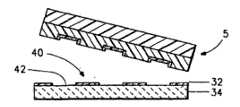
如图3所示,包括载体16的压模5通过剥离与母模12分离。因为在压模5上的载体16具有足够的挠性,所以载体和压模能承受从母模12分离时所需的弯曲。载体16保留有固化的弹性体层24,为压模5提供复制与软性平版印刷方法相关的微型图案和微结构所需的尺寸稳定性。压模5在与载体16相反的一面包括浮雕表面26,该浮雕表面具有与母模12的浮雕图案13的负片对应的凹陷表面28和凸起表面30。浮雕表面26在凸起部分30和凹陷部分28之间具有不同的高度,即浮雕深度。压模5的浮雕结构26形成用于在基材34上印刷掩模材料32的凸起表面30以及不进行印刷的凹陷表面部分28的图案。As shown in FIG. 3, the
图4中,如一个实施方式,压模5放置在旋涂设备的平台35上,用于将掩模材料32施涂到压模5的浮雕结构26上。将掩模材料32施涂至压模5的浮雕结构26,旋转该平台以形成相对均匀连续的掩模材料层。In FIG. 4 , the
图5中,将具有掩模材料层32的压模5和基材34彼此相邻放置,使得在压模5的凸起表面30上的掩模材料与基材34的表面38接触。In FIG. 5 ,
图6中,压模5与基材34分离,与基材接触的掩模材料32保留在基材上,转移以形成掩模材料的图案40。基材34包括掩模材料32的图案40以及没有掩模材料的敞开区域42。In FIG. 6, the
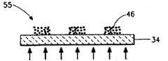
图7中,如一个实施方式,具有掩模图案40的基材34设置在旋涂设备的平台35上,用于将功能材料46施涂至基材。将功能材料46施涂到基材34具有掩模图案40的一侧,旋转平台35以在基材上形成相对均匀连续的功能材料46的层。在所示的实施方式中,功能材料46的层同时覆盖了掩模材料32的图案40以及敞开区域42。In FIG. 7, as one embodiment, a
图8中,将具有功能材料层46和掩模图案40的基材34放置在含溶液52的浴液50中,所述溶液是用于掩模材料32的溶剂。掩模材料32的图案40剥离(lift)基材34和/或溶解于溶液浴50中。位于掩模图案40上的功能材料46也可以与掩模材料32一起除去,位于敞开区域42的功能材料46可保留在基材34上。位于基材34的敞开区域42上的功能材料46形成用于电子器件或元件的功能材料46的图案55。In FIG. 8 , the
图9中,如进行进一步处理的实施方式,可以对具有功能材料46的图案55的基材34进行加热。在该实施方式中,功能材料46是金属纳米颗粒,所述金属纳米颗粒需要通过加热而烧结,以使图案55具备导电性。In FIG. 9,
实施例Example
除非另外指出,否则,所有百分数都是以组合物的总重量为基准的。All percentages are by weight of the total composition, unless otherwise indicated.
实施例1Example 1
下面的实施例说明了在基材上形成图案的方法。用银纳米颗粒在挠性基材上形成图案,可提供薄膜晶体管的功能源-漏水平(source-drain level)。The following examples illustrate methods of forming patterns on substrates. Patterning of flexible substrates with silver nanoparticles provides a functional source-drain level for thin film transistors.
母模制备:Master mold preparation :
在2英寸(5.1厘米)硅晶片上,以3000rpm旋涂六甲基二硅氮烷薄层(HMDS)(得自奥尔德里奇(Aldrich))60秒。HMDS是用于在硅晶片上的光刻胶材料的增粘剂。以3000rpm在HMDS层上旋涂斯谱立(Shipley)正性光刻胶(型号1811,得自罗门哈斯(Rohm and Haas))60秒。将该光刻胶膜在115℃的热板上预烘焙1分钟以完全干燥。然后,在I-划线器(liner)(OAI掩模校准器,型号200(OAI Mask Aligner,Model 200))中,该预烘焙的光刻胶膜通过光掩模在365纳米的紫外光辐照中以成像方式曝光8秒。曝光后,将该光刻胶在型号MF-319(得自罗门哈斯)的显影剂中显影60秒,该显影剂是四甲基氢氧化铵(TMAH)溶液。显影后的膜在蒸馏水中清洗,用氮气干燥,并在115℃的热板上加热5分钟,形成带浮雕图案的母模。在制成的母模上的浮雕图案具有凸起表面区域和凹陷区域。母模中的凸起表面区域形成正性图像,该图像将是形成在基材上的功能材料银的图案。用表面轮廓仪(加利福尼亚州圣何塞的KLA-Tencor(KLA-Tencor,San Jose,CA))测量,母模上图案化的光刻胶层厚度为1.1微米。HMDS保留在母模的凹陷区域中。A thin layer of hexamethyldisilazane (HMDS) (from Aldrich) was spin-coated at 3000 rpm for 60 seconds on a 2 inch (5.1 cm) silicon wafer. HMDS is an adhesion promoter for photoresist materials on silicon wafers. Shipley positive photoresist (type 1811 from Rohm and Haas) was spin-coated on the HMDS layer at 3000 rpm for 60 seconds. The photoresist film was prebaked on a hot plate at 115° C. for 1 minute to dry completely. Then, in an I-scriber (liner) (OAI Mask Aligner, Model 200 (OAI Mask Aligner, Model 200)), the photoresist film of this prebaking is passed through a photomask under 365 nm ultraviolet radiation Images were exposed imagewise for 8 seconds. After exposure, the photoresist was developed for 60 seconds in developer model MF-319 (from Rohm and Haas), which was a solution of tetramethylammonium hydroxide (TMAH). The developed film was rinsed in distilled water, dried with nitrogen, and heated on a hot plate at 115 °C for 5 min to form a master mold with a relief pattern. The relief pattern on the finished master has raised surface areas and recessed areas. The raised surface areas in the master form a positive image that will be the pattern of the functional material silver formed on the substrate. The photoresist layer patterned on the master was 1.1 microns thick as measured by a surface profiler (KLA-Tencor, San Jose, CA). The HMDS remains in the recessed areas of the master mold.
弹性压模的制备:Preparation of the elastic stamper:
按照以下方式制备用于弹性压模的载体:通过旋涂方法,以3000rpm在5密耳(0.0127厘米)的
使用由宾夕法尼亚州爱斯通的萨托玛(Sartomer,Exton,PA)提供的产品型号为CN4000的全氟聚醚(PFPE)化合物E10-DA,不进行处理直接使用。E10-DA具有以下结构式:Perfluoropolyether (PFPE) compound E10-DA, product number CN4000, supplied by Sartomer, Exton, PA, was used without treatment. E10-DA has the following structural formula:
R-E-CF2-O-(CF2-O-)n(-CF2-CF2-O-)m-CF2-E’-R’RE-CF2 -O-(CF2 -O-)n (-CF2 -CF2 -O-)m -CF2 -E'-R'
其中,R和R’各自是丙烯酸酯,E是(CH2CH2O)1-2CH2的直链非氟化的烃醚,E’是(CF2CH2O(CH2CH2O)1-2的直链烃醚,分子量约为1000。确定E10-DA是PFPE二丙烯酸酯的预聚物。wherein R and R' are each acrylate, E is a linear non-fluorinated hydrocarbon ether of (CH2 CH2 O)1-2 CH2 , E' is (CF2 CH2 O(CH2 CH2 O )1-2 linear hydrocarbon ether, the molecular weight is about 1000. It is determined that E10-DA is a prepolymer of PFPE diacrylate.
按以下方式制备弹性压模组合物:混合PFPE二丙烯酸酯预聚物(MW 1000)和1重量%的光引发剂Darocur 1173(得自瑞士巴塞尔的汽巴专用化学品公司(from Ciba Specialty Chemicals,Basel,Switzerland))。Darocur 1173的结构如下。An elastic compression molding composition was prepared in the following manner: PFPE diacrylate prepolymer (MW 1000) was mixed with 1% by weight of photoinitiator Darocur 1173 (from Ciba Specialty Chemicals, Basel, Switzerland) , Basel, Switzerland)). The structure of Darocur 1173 is as follows.

该混合物用0.45微米的PTFE过滤器进行过滤。将过滤后的预聚物倒入,在制成的母模具有浮雕图案的一侧形成一个层。将该载体放置在与母模相反的PFPE预聚物层(空气层界面)上,使粘合剂与该层接触。在氮气气氛中,使用365纳米I-划线器,使PFPE层通过载体曝光10分钟,以固化或聚合PFPE层,形成压模。然后将压模从母模上剥离,该压模具有与母模中的浮雕图案相反的浮雕表面。因此,压模上的浮雕表面是所需功能材料的图案的负片。(即,压模具有凸起表面部分和凹陷表面部分,所述凹陷表面部分对应于最终将形成的银图案。)The mixture was filtered through a 0.45 micron PTFE filter. The filtered prepolymer is poured to form a layer on the embossed side of the resulting master mold. The carrier was placed on the PFPE prepolymer layer opposite the master tool (air layer interface) with the adhesive in contact with this layer. The PFPE layer was cured or polymerized by exposing the PFPE layer through the carrier using a 365 nm I-scriber for 10 minutes in a nitrogen atmosphere to form a stamp. The stamper, which has a relief surface opposite to the relief pattern in the master mold, is then peeled from the master. Thus, the relief surface on the stamp is a negative of the pattern of the desired functional material. (That is, the stamper has a raised surface portion and a recessed surface portion corresponding to the silver pattern that will eventually be formed.)
压模上的浮雕图案凸起部分的高度为0.4微米,宽度在5-500微米范围变化;凹陷部分的宽度在2-20000微米范围变化。The height of the raised part of the embossed pattern on the stamper is 0.4 microns, and the width varies in the range of 5-500 microns; the width of the concave part changes in the range of 2-20000 microns.
掩模材料的转移:Transfer of mask material:
将掩模材料0.5重量%的Covion Super-YellowTM(取代的(1,4-亚苯基-亚乙烯基)共聚物(得自墨克(Merck))的溶液溶于甲苯中,并用1微米的PTFE过滤器进行过滤。以3000rpm,将该掩模材料溶液旋涂至制成的PFPE压模的浮雕表面上60秒。该溶液覆盖全部浮雕表面,使其在空气中室温干燥约1分钟。在保持65℃的热板上放置一基材,即5密耳的膜(型号ST504)。将具有掩模材料层的PFPE压模层叠在基材的丙烯酸侧(在热板上时),但不施加任何附加压力。从热板上取下压模和基材,在室温将压模与基材分离。在弹性压模的浮雕图案的凸起表面上的牺牲掩模材料转移至基材,并在基材上形成掩模图案。压模中的凹陷区域不与基材接触,因此,基材具有不含掩模材料的敞开区域。用轮廓仪测量,掩模材料的图案的厚度为27纳米。印刷的牺牲掩模材料的压模图案是母模上图案的正片(即,印刷的母模图案与母模的凹陷区域的图案相同)。A solution of 0.5% by weight of the masking material Covion Super-Yellow™ (a substituted (1,4-phenylene-vinylene) copolymer (from Merck)) was dissolved in toluene and washed with 1 micron Filtered with a PTFE filter. Spin-coat the mask material solution at 3000 rpm on the relief surface of the PFPE stamper made for 60 seconds. The solution covers the entire relief surface and is allowed to dry in air at room temperature for about 1 minute. Place a substrate on a hot plate maintained at 65°C, 5 mil Membrane (Model ST504). A PFPE stamp with a layer of masking material was laminated to the acrylic side of the substrate (while on the hot plate) without applying any additional pressure. Remove the stamp and substrate from the hot plate and separate the stamp from the substrate at room temperature. The sacrificial mask material on the raised surface of the relief pattern of the elastomeric stamper is transferred to the substrate and forms a mask pattern on the substrate. The recessed areas in the stamp are not in contact with the substrate, so the substrate has open areas free of masking material. The thickness of the pattern of mask material was measured with a profilometer to be 27 nm. The stamp pattern of the printed sacrificial mask material is a positive of the pattern on the master (ie, the printed pattern of the master is the same as the pattern of the recessed areas of the master).
功能材料的图案化:Patterning of functional materials:
从韩国阿纳帕(Anapro,Korea)购得具有45%固体的银油墨,型号DGP-MP-40LT。该银油墨具有直径50纳米的银纳米颗粒。用乙醇将该油墨稀释至17重量%。然后,该稀释的银分散体用尖端声波处理器(tip sonicator)进行声波处理5分钟,并用0.2微米PTFE过滤器过滤两次。以3000rpm将该银分散体旋涂到具有牺牲材料的掩模图案的基材上60秒。基材的全部表面被该银分散体覆盖,即银材料以层形式沉积在掩模图案和敞开区域上。然后,所述银于65℃退火1分钟,以除去溶剂,并于140℃在热板上烧结5分钟。将具有掩模和功能层的基材置于氯仿浴液中,该浴液声波处理1分钟,以剥离该掩模。将牺牲掩模材料从基材上剥离去除还会附带上沉积在该掩模顶部的银,但是不会影响直接施涂至基材的银。功能银材料的图案保留在基材上。在基材上的银图案用异丙醇(IPA)和蒸馏水清洗,并用氮气喷枪干燥。A silver ink with 45% solids was purchased from Anapro, Korea, model number DGP-MP-40LT. The silver ink has silver nanoparticles with a diameter of 50 nm. The ink was diluted to 17% by weight with ethanol. The diluted silver dispersion was then sonicated with a tip sonicator for 5 minutes and filtered twice with a 0.2 micron PTFE filter. The silver dispersion was spin-coated onto a substrate with a masked pattern of sacrificial material at 3000 rpm for 60 seconds. The entire surface of the substrate is covered with the silver dispersion, ie the silver material is deposited in a layer on the mask pattern and the open areas. The silver was then annealed at 65°C for 1 minute to remove the solvent and sintered on a hot plate at 140°C for 5 minutes. The substrate with the mask and functional layer was placed in a chloroform bath that was sonicated for 1 minute to peel off the mask. Stripping and removing the sacrificial mask material from the substrate also carries with it the silver deposited on top of the mask, but does not affect the silver applied directly to the substrate. The pattern of functional silver material remains on the substrate. The silver pattern on the substrate was cleaned with isopropanol (IPA) and distilled water, and dried with a nitrogen spray gun.
基材上用图案形成含集成的源-漏线条的元件。线条宽度为5微米。源漏线条的间隔为2微米。银图案线条的电阻率小于2欧姆/□(ohm/sq.)。A device with integrated source-drain lines is patterned on the substrate. The line width is 5 microns. The interval between source and drain lines is 2 microns. The resistivity of the silver pattern lines is less than 2 ohms/square (ohm/sq.).
采用这种方法进行图案化产生的源漏线条没有中断或不希望的微粒。与标准微接触印刷(参见比较例)不同,没有在名义清洁的背景区域上发生不希望的银转移。线条是高度脆性的,图像与通过光刻法获得的图像类似。Patterning in this way produces source-drain lines without interruptions or unwanted particles. Unlike standard microcontact printing (see comparative example), no unwanted silver transfer occurred on the nominally clean background areas. The lines are highly brittle and the images are similar to those obtained by photolithography.
实施例2Example 2
下面实施例说明了使用弹性压模以印刷牺牲掩模材料,形成功能材料的图案的方法。功能材料是在挠性膜基材上形成图案的银纳米颗粒。The following examples illustrate the use of elastic stampers to print sacrificial masking materials to form patterns of functional materials. The functional material is silver nanoparticles patterned on a flexible film substrate.
按照实施例1中所述制备母模和弹性压模。压模上的浮雕图案具有和实施例1中所列相同的尺寸。Master and elastic stampers were prepared as described in Example 1. The relief pattern on the stamp had the same dimensions as listed in Example 1.
牺牲材料的转移:Transfer of sacrificial material:
通过以下方式制备聚(4-乙烯基吡啶)(P4VP)溶液(得自奥尔德里奇,St Louis,MO)的牺牲掩模材料:将1重量%的P4VP聚合物溶于氯仿(CCl3H)中,并用0.2微米的PTFE过滤器过滤。以3000rpm将该P4VP溶液旋涂在弹性PFPE压模上60秒,并空气干燥约1分钟。然后,于室温将PFPE压模上的P4VP印刷到作为基材的5密耳
功能材料的图案化:Patterning of functional materials:
从韩国阿纳帕(Anapro,Korea)购得具有45重量%固体的银油墨,型号DGH。该银油墨具有直径约20纳米的银纳米颗粒。用甲苯将该油墨稀释至18重量%。然后,该稀释的银分散体用尖端声波处理器(tip sonicator)进行声波处理10分钟,并用0.2微米PTFE过滤器过滤两次。以2000rpm将该银溶液旋涂到具有牺牲材料P4VP的掩模图案的基材上60秒。基材的全部表面被该银分散体覆盖,即银材料以层形式沉积在掩模图案和敞开区域上。然后,该银层在热板上于130℃退火10分钟。将具有掩模层和功能层的基材置于甲醇(MeOH)浴液中,该浴液声波处理1分钟,以剥离该掩模。将牺牲材料P4VP从基材上剥离去除还会附带上沉积在该掩模顶部的银,但是不会影响直接旋涂在基材上的银。在基材上的银图案用新鲜的甲醇和蒸馏水清洗,并用氮气喷枪干燥。基材上的银图案于140℃烧结48小时。银图案线条的电阻率为4.4欧姆/□。A silver ink with 45% by weight solids was purchased from Anapro, Korea, model DGH. The silver ink has silver nanoparticles about 20 nanometers in diameter. The ink was diluted to 18% by weight with toluene. The diluted silver dispersion was then sonicated with a tip sonicator for 10 minutes and filtered twice with a 0.2 micron PTFE filter. The silver solution was spin-coated at 2000 rpm for 60 seconds on a substrate with a mask pattern of sacrificial material P4VP. The entire surface of the substrate is covered with the silver dispersion, ie the silver material is deposited in a layer on the mask pattern and the open areas. The silver layer was then annealed on a hot plate at 130°C for 10 minutes. The substrate with the mask layer and the functional layer was placed in a methanol (MeOH) bath that was sonicated for 1 minute to lift off the mask. Lifting and removing the sacrificial material P4VP from the substrate also carries with it the silver deposited on top of this mask, but does not affect the silver spun directly onto the substrate. The silver patterns on the substrate were cleaned with fresh methanol and distilled water, and dried with a nitrogen spray gun. The silver pattern on the substrate was sintered at 140°C for 48 hours. The resistivity of the silver pattern lines was 4.4 ohm/□.
对20纳米银颗粒的延长加热将这些颗粒烧结成基材上的导电膜。虽然DGH型号的银纳米颗粒在约250℃能快速烧结,但是
具有烧结的银线条的基材用丙酮清洗,以从基材去除松散的颗粒。产生的功能银材料的图案不含颗粒。基材上的银图案形成20个晶体管的源-漏水平,每个晶体管具有17根集成的源-漏线条。该图案包括5微米的线条,以及3微米,5微米和8微米的沟槽。The substrate with the sintered silver lines was rinsed with acetone to remove loose particles from the substrate. The resulting pattern of functional silver material is grain-free. The silver pattern on the substrate forms a source-drain level of 20 transistors each with 17 integrated source-drain lines. The pattern includes 5 micron lines, and 3 micron, 5 micron and 8 micron grooves.
回顾具有5微米线条和间隔的集成源漏所形成的图案在丙酮清洗之前和之后的详细图像。清楚观察到在延长加热后在基材表面上形成了颗粒(粒度为0.5-5微米)。颗粒数量在整个表面上变化,因为源漏的左电极具有约50个颗粒,而右电极的颗粒较少。在每个线条上的颗粒数量也不同。预清洗的图像显示每根线条上有1-10个颗粒。集成的源漏在丙酮漂洗后的图像中,对银图案的线条进行清洁,没有观察到线条中的任何颗粒和中断。Review of detailed images of patterns formed by an integrated source-drain with 5 μm lines and spaces before and after acetone cleaning. The formation of particles (particle size 0.5-5 microns) on the substrate surface was clearly observed after prolonged heating. The number of particles varies across the surface, as the left electrode of the source drain has about 50 particles, while the right electrode has fewer particles. The number of particles on each line is also different. Pre-washed images show 1-10 particles per line. The integrated source-drain cleans the lines of the silver pattern in the image after rinsing with acetone, without observing any grains and discontinuities in the lines.
实施例3Example 3
下面实施例说明在挠性膜上形成功能材料的图案的方法。功能材料是聚噻吩的有机半导体材料。The following examples illustrate methods of forming patterns of functional materials on flexible films. The functional material is an organic semiconductor material of polythiophene.
按照实施例1中所述制备母模和弹性压模。Master and elastic stampers were prepared as described in Example 1.
掩模材料的转移:Transfer of mask material:
制备下面结构式所示的TFE-NB-f-OH共聚物(2-丙醇,2-[(双环[2.2.1]庚-5-烯-2-基氧基)甲基]-1,1,1,3,3,3-六氟-)聚合物与四氟乙烯溶解在丙酮中的10重量%的溶液。Prepare TFE-NB-f-OH copolymer (2-propanol, 2-[(bicyclo[2.2.1]hept-5-en-2-yloxy)methyl]-1,1 shown in the following structural formula , 1,3,3,3-hexafluoro-) polymer and tetrafluoroethylene dissolved in acetone 10% by weight solution.

制备1重量%
功能材料的图案化:Patterning of functional materials:
以5000rpm,将0.5重量%的聚噻吩的氯仿溶液旋涂至基材上60秒。基材的全部表面被聚噻吩溶液覆盖,即聚噻吩以层形式沉积在掩模图案和敞开区域上。将具有掩模和功能材料层的基材置于丙酮浴液中,该浴液声波处理10秒,以剥离去除在聚噻吩层下面的掩模材料的图案。A 0.5% by weight solution of polythiophene in chloroform was spin-coated onto the substrate at 5000 rpm for 60 seconds. The entire surface of the substrate is covered with the polythiophene solution, ie the polythiophene is deposited in a layer on the mask pattern and the open areas. The substrate with the mask and functional material layer was placed in an acetone bath that was sonicated for 10 seconds to lift off the pattern of masking material underneath the polythiophene layer.
将掩模材料从基材上剥离去除还会附带上沉积在该掩模顶部的聚噻吩材料,但是不会影响直接施涂在基材上的聚噻吩材料。没有外来的银材料留下或沉积在银的图案线条之间。聚噻吩的图案线条宽度约为200微米,显示有一些微粒。Stripping and removing the mask material from the substrate also carries with it the polythiophene material deposited on top of the mask, but does not affect the polythiophene material applied directly on the substrate. No extraneous silver material is left or deposited between the silver pattern lines. The polythiophene pattern has a line width of approximately 200 microns, showing some particulates.
实施例4Example 4
下面实施例说明了使用弹性压模以印刷牺牲掩模材料,形成功能材料的图案的方法。功能材料是在挠性膜基材上形成图案的银纳米颗粒。The following examples illustrate the use of elastic stampers to print sacrificial masking materials to form patterns of functional materials. The functional material is silver nanoparticles patterned on a flexible film substrate.
按照实施例1中所述制备母模和弹性压模。压模上的浮雕图案具有和实施例1中所列相同的尺寸。凸起部分的宽度为5-500微米,高度为0.4微米,凹陷部分的宽度为2-20000微米,高度为0.4微米。Master and elastic stampers were prepared as described in Example 1. The relief pattern on the stamp had the same dimensions as listed in Example 1. The raised part has a width of 5-500 microns and a height of 0.4 microns, and the depressed part has a width of 2-20000 microns and a height of 0.4 microns.
牺牲材料的转移:Transfer of sacrificial material:
制备掩模材料。制备1重量%的三芳基胺聚合物的甲苯溶液。按照Herron等在公开的PCT申请WO 2005/080525的实施例1中所述,制备以下结构式的三芳基胺聚合物:Prepare mask material. A 1% by weight triarylamine polymer solution in toluene was prepared. Triarylamine polymers of the following formula were prepared as described by Herron et al. in Example 1 of published PCT application WO 2005/080525:
制备1重量%的

功能材料的图案化:Patterning of functional materials:
从韩国阿纳帕(Anapro,Korea)购得具有45重量%固体的银油墨,型号DGH。该银油墨具有直径约20纳米的银纳米颗粒。用甲苯将该油墨稀释至18重量%。然后,该稀释的银分散体用尖端声波处理器(tip sonicator)进行声波处理10分钟,并用0.2微米PTFE过滤器过滤两次。以2000rpm将该银溶液旋涂到具有掩模材料的图案的基材上60秒。基材的全部表面被该银分散体覆盖,即银材料以层形式沉积在掩模图案和敞开区域上。然后,该银层在热板上于130℃退火20分钟。将具有掩模和功能层的基材置于氯仿(CHCl3)浴液中,该浴液声波处理1分钟,以剥离去除该掩模。将牺牲掩模材料从基材上剥离去除还会附带上沉积在该掩模顶部的银,但是不会影响直接旋涂在基材上的银。在基材上的银图案用新鲜的异丙醇和蒸馏水清洗,并用氮气喷枪干燥。基材上的银图案于140℃烧结48小时。A silver ink with 45% by weight solids was purchased from Anapro, Korea, model DGH. The silver ink has silver nanoparticles about 20 nanometers in diameter. The ink was diluted to 18% by weight with toluene. The diluted silver dispersion was then sonicated with a tip sonicator for 10 minutes and filtered twice with a 0.2 micron PTFE filter. The silver solution was spin-coated onto the substrate with the pattern of masking material at 2000 rpm for 60 seconds. The entire surface of the substrate is covered with the silver dispersion, ie the silver material is deposited in a layer on the mask pattern and the open areas. The silver layer was then annealed on a hot plate at 130°C for 20 minutes. The substrate with the mask and functional layer was placed in a chloroform (CHCl3 ) bath that was sonicated for 1 minute to lift off the mask. Stripping and removing the sacrificial mask material from the substrate also carries with it the silver deposited on top of the mask, but does not affect the silver spun directly onto the substrate. The silver pattern on the substrate was cleaned with fresh isopropanol and distilled water, and dried with a nitrogen jet. The silver pattern on the substrate was sintered at 140°C for 48 hours.
回顾具有5微米线条和20-2微米间隔的集成源漏所形成的掩模材料图案在氯仿清洗之前和之后的详细图像。集成源漏的掩模图案的图像显示PEPE母模的高分辨的清晰边缘。该图案银的分辨率为5微米线条和5微米间隔。Review of detailed images of masking material patterns formed by integrated source-drains with 5 µm lines and 20-2 µm spaces before and after chloroform cleaning. The image of the mask pattern for the integrated source-drain shows high-resolution sharp edges of the PEPE master. The patterned silver has a resolution of 5 micron lines and 5 micron spaces.
比较例comparative example
以下比较例说明功能材料的直接接触印刷,其中,将功能材料转移至基材上不应有功能材料的无特征区域。The following comparative examples illustrate direct contact printing of functional materials where the functional material is transferred to featureless areas on the substrate where the functional material should not be present.
母模制备:Master mold preparation :
使用负性光刻胶,SU-8型2(得自马塞诸斯州纽顿(Newton,MA)的MICRO CHEM),并采用实施例1中使用的相同光掩模,制造带图案的母模。因此,由这种母模形成的压模的凸起表面可用于直接将功能材料印刷在基材上。该光刻胶以7∶3的重量比用γ丁内酯稀释,并用1.0微米的PTFE过滤。以3000rpm将该溶液旋涂至硅晶片上,于65℃干燥1分钟,并于95℃预烘焙1分钟。将该预烘焙的光刻胶用I-划线器(365nm)曝光5秒,然后在95℃热板上后烘焙1分钟。将在硅晶片上的后烘焙的光刻胶在SU-8显影剂(得自MICRO CHEM)中显影1分钟,用异丙醇和蒸馏水清洗,用氮气喷枪干燥。用轮廓仪测量,光刻胶图案的特征高度为400纳米。Using a negative tone photoresist, SU-8 Type 2 (available from MICRO CHEM, Newton, MA), and employing the same photomask used in Example 1, a patterned master was fabricated. mold. Thus, the raised surface of a stamp formed from such a master can be used to print functional materials directly onto substrates. The photoresist was diluted with gamma butyrolactone at a weight ratio of 7:3 and filtered through 1.0 micron PTFE. The solution was spin-coated onto a silicon wafer at 3000 rpm, dried at 65°C for 1 minute, and prebaked at 95°C for 1 minute. The prebaked photoresist was exposed with an I-scriber (365 nm) for 5 seconds and then post-baked on a 95° C. hot plate for 1 minute. The post-baked photoresist on the silicon wafer was developed in SU-8 developer (from MICRO CHEM) for 1 minute, rinsed with isopropanol and distilled water, and dried with a nitrogen spray gun. The photoresist pattern has a feature height of 400 nm as measured with a profilometer.
按照实施例1所述的方式,由该母模制造弹性压模。In the manner described in Example 1, an elastic stamper was fabricated from this master mold.
功能材料的转移:Transfer of functional materials:
从韩国阿纳帕(Anapro,Korea)购得具有45重量%固体的银油墨,型号DGH。用甲苯将该油墨稀释至18重量%。然后,该稀释的银分散体用尖端声波处理器(tipsonicator)进行声波处理10分钟,并用0.2微米PTFE过滤器过滤两次。以2000rpm将该银溶液旋涂至PEPE压模60秒。该压模的表面完全被银分散体覆盖。该银层空气干燥1分钟,通过施加常规压力,银层转移至基材的涂覆丙烯酸侧。基材是5密耳的
对于该比较例和实施例2,图像取自基材上银源漏线条的图案,然后进行比较。该比较例产生的银图案的图像示于图10a。实施例2产生的银图案的图像示于图10b。采用比较例所述的直接微接触印刷形成的银图案显示功能银材料被印刷在不应有功能材料的敞开区域中。此外,银图案的线条中断,并观察到基材上有微粒。在中心周围的较大区域以及晶体管垫之间的较大区域中,由于弹性压模的凹陷部分的下垂,银被印刷沉积在基材上。For this Comparative Example and Example 2, images were taken of the pattern of silver source-drain lines on the substrate and then compared. An image of the silver pattern produced by this comparative example is shown in Figure 10a. An image of the silver pattern produced in Example 2 is shown in Figure 10b. Silver patterns formed using direct microcontact printing as described in the comparative example show that functional silver material is printed in open areas where there should be no functional material. In addition, the lines of the silver pattern were interrupted and particles were observed on the substrate. In the larger area around the center and in the larger area between the transistor pads, silver is print-deposited on the substrate due to the sagging of the recessed portion of the elastic stamp.
该银印刷的图案包括在顶部和底部的20个电极。电极宽度为0.5毫米,电极之间的间隔也为0.5毫米。如在图10a的图像中观察的,在电极之间的21个间隔中有16个间隔有转移的另外的银,是因为印刷期间压模的下垂产生的。位于中心左面和右面的三角形区域的面积约为40毫米2,该中心以集成的最外的源和漏线条的对角线以及字母A和B界定。左面(字母A)的三角形区域的约100%的区域以及在右面(字母B)的三角形区域的约70-80%的区域被转移的银覆盖,原因是压模下垂。The silver printed pattern included 20 electrodes on the top and bottom. The electrode width is 0.5 mm, and the interval between electrodes is also 0.5 mm. As observed in the image of Figure 10a, 16 of the 21 spaces between the electrodes had additional silver transferred due to sagging of the stamp during printing. The area of the triangular area to the left and right of the center is about 40 mm2 , which is bounded by the diagonals of the integrated outermost source and drain lines and the letters A and B. About 100% of the area of the triangular area on the left (letter A) and about 70-80% of the area of the triangular area on the right (letter B) were covered with transferred silver due to stamper sagging.
如在图10b的图像中观察的,使用实施例2所述的掩模材料层制成的银图案显示形成优良导电的银图案,因为在电极之间的所有21个间隔都是清洁的没有被转移至图案区域之外的任何银。此外,上述三角形区域显示没有银的转移。比较这些图像后表明,当按照比较例的方法印刷导体时,压模下垂造成不希望的功能材料转移,很清楚这种转移可能导致各种晶体管线路的短路,而本发明的方法基本上消除了线路短路的可能性。本发明方法避免了功能材料在特征线条之间和周围的不希望的转移,并避免在背景区域形成功能材料。As observed in the image of Figure 10b, the silver pattern made using the masking material layer described in Example 2 shows the formation of a silver pattern with excellent conductivity because all 21 spaces between the electrodes are clean and not Transfer to any silver outside the patterned area. Furthermore, the aforementioned triangular area shows no transfer of silver. Comparing these images shows that when the conductors are printed according to the method of the comparative example, the stamper sags causing unwanted functional material transfer, which clearly can lead to short circuits of various transistor lines, whereas the method of the present invention substantially eliminates Possibility of short circuit. The inventive method avoids unwanted transfer of functional material between and around feature lines and avoids formation of functional material in background areas.
Claims (29)

Applications Claiming Priority (3)
| Application Number | Priority Date | Filing Date | Title |
|---|---|---|---|
| US11/508,806US20080047930A1 (en) | 2006-08-23 | 2006-08-23 | Method to form a pattern of functional material on a substrate |
| US11/508,806 | 2006-08-23 | ||
| PCT/US2007/017670WO2008024207A1 (en) | 2006-08-23 | 2007-08-08 | Method to form a pattern of functional material on a substrate |
Publications (2)
| Publication Number | Publication Date |
|---|---|
| CN101505969A CN101505969A (en) | 2009-08-12 |
| CN101505969Btrue CN101505969B (en) | 2010-09-01 |
Family
ID=38920776
Family Applications (1)
| Application Number | Title | Priority Date | Filing Date |
|---|---|---|---|
| CN2007800311719AExpired - Fee RelatedCN101505969B (en) | 2006-08-23 | 2007-08-08 | Method to form a pattern of functional material on a substrate |
Country Status (7)
| Country | Link |
|---|---|
| US (1) | US20080047930A1 (en) |
| EP (1) | EP2054233B1 (en) |
| JP (1) | JP2010502010A (en) |
| KR (1) | KR20090042848A (en) |
| CN (1) | CN101505969B (en) |
| DE (1) | DE602007009544D1 (en) |
| WO (1) | WO2008024207A1 (en) |
Families Citing this family (75)
| Publication number | Priority date | Publication date | Assignee | Title |
|---|---|---|---|---|
| US20100038121A1 (en)* | 1999-08-27 | 2010-02-18 | Lex Kosowsky | Metal Deposition |
| US20100044080A1 (en)* | 1999-08-27 | 2010-02-25 | Lex Kosowsky | Metal Deposition |
| WO2001017320A1 (en)* | 1999-08-27 | 2001-03-08 | Lex Kosowsky | Current carrying structure using voltage switchable dielectric material |
| US7825491B2 (en) | 2005-11-22 | 2010-11-02 | Shocking Technologies, Inc. | Light-emitting device using voltage switchable dielectric material |
| US20100044079A1 (en)* | 1999-08-27 | 2010-02-25 | Lex Kosowsky | Metal Deposition |
| US20100038119A1 (en)* | 1999-08-27 | 2010-02-18 | Lex Kosowsky | Metal Deposition |
| EP1969627A4 (en) | 2005-11-22 | 2010-01-20 | Shocking Technologies Inc | SEMICONDUCTOR DEVICES COMPRISING VOLTAGE SWITCHING MATERIALS PROVIDING OVERVOLTAGE PROTECTION |
| US7968014B2 (en) | 2006-07-29 | 2011-06-28 | Shocking Technologies, Inc. | Device applications for voltage switchable dielectric material having high aspect ratio particles |
| WO2008036423A2 (en) | 2006-09-24 | 2008-03-27 | Shocking Technologies, Inc. | Formulations for voltage switchable dielectric material having a stepped voltage response and methods for making the same |
| US8128393B2 (en) | 2006-12-04 | 2012-03-06 | Liquidia Technologies, Inc. | Methods and materials for fabricating laminate nanomolds and nanoparticles therefrom |
| GB0701909D0 (en)* | 2007-01-31 | 2007-03-14 | Imp Innovations Ltd | Deposition Of Organic Layers |
| US8083953B2 (en) | 2007-03-06 | 2011-12-27 | Micron Technology, Inc. | Registered structure formation via the application of directed thermal energy to diblock copolymer films |
| US8557128B2 (en) | 2007-03-22 | 2013-10-15 | Micron Technology, Inc. | Sub-10 nm line features via rapid graphoepitaxial self-assembly of amphiphilic monolayers |
| US7875313B2 (en)* | 2007-04-05 | 2011-01-25 | E. I. Du Pont De Nemours And Company | Method to form a pattern of functional material on a substrate using a mask material |
| US8097175B2 (en)* | 2008-10-28 | 2012-01-17 | Micron Technology, Inc. | Method for selectively permeating a self-assembled block copolymer, method for forming metal oxide structures, method for forming a metal oxide pattern, and method for patterning a semiconductor structure |
| US8294139B2 (en)* | 2007-06-21 | 2012-10-23 | Micron Technology, Inc. | Multilayer antireflection coatings, structures and devices including the same and methods of making the same |
| US7959975B2 (en) | 2007-04-18 | 2011-06-14 | Micron Technology, Inc. | Methods of patterning a substrate |
| US8372295B2 (en) | 2007-04-20 | 2013-02-12 | Micron Technology, Inc. | Extensions of self-assembled structures to increased dimensions via a “bootstrap” self-templating method |
| US8404124B2 (en) | 2007-06-12 | 2013-03-26 | Micron Technology, Inc. | Alternating self-assembling morphologies of diblock copolymers controlled by variations in surfaces |
| US7793236B2 (en) | 2007-06-13 | 2010-09-07 | Shocking Technologies, Inc. | System and method for including protective voltage switchable dielectric material in the design or simulation of substrate devices |
| US8080615B2 (en) | 2007-06-19 | 2011-12-20 | Micron Technology, Inc. | Crosslinkable graft polymer non-preferentially wetted by polystyrene and polyethylene oxide |
| GB2453766A (en)* | 2007-10-18 | 2009-04-22 | Novalia Ltd | Method of fabricating an electronic device |
| US8999492B2 (en) | 2008-02-05 | 2015-04-07 | Micron Technology, Inc. | Method to produce nanometer-sized features with directed assembly of block copolymers |
| US8101261B2 (en) | 2008-02-13 | 2012-01-24 | Micron Technology, Inc. | One-dimensional arrays of block copolymer cylinders and applications thereof |
| JP5301176B2 (en)* | 2008-02-29 | 2013-09-25 | 積水化学工業株式会社 | Micropattern manufacturing method |
| US8426313B2 (en) | 2008-03-21 | 2013-04-23 | Micron Technology, Inc. | Thermal anneal of block copolymer films with top interface constrained to wet both blocks with equal preference |
| US8425982B2 (en) | 2008-03-21 | 2013-04-23 | Micron Technology, Inc. | Methods of improving long range order in self-assembly of block copolymer films with ionic liquids |
| US8203421B2 (en) | 2008-04-14 | 2012-06-19 | Shocking Technologies, Inc. | Substrate device or package using embedded layer of voltage switchable dielectric material in a vertical switching configuration |
| US8114301B2 (en) | 2008-05-02 | 2012-02-14 | Micron Technology, Inc. | Graphoepitaxial self-assembly of arrays of downward facing half-cylinders |
| WO2009143378A1 (en)* | 2008-05-21 | 2009-11-26 | Northwestern University | Generation of photomasks by dip-pen nanolithography |
| AT507353B1 (en)* | 2008-09-29 | 2012-04-15 | Hueck Folien Gmbh | METHOD OF STRUCTURING INORGANIC OR ORGANIC LAYERS |
| KR101653426B1 (en) | 2008-09-30 | 2016-09-01 | 쇼킹 테크놀로지스 인코포레이티드 | Voltage switchable dielectric material containing conductive core shelled particles |
| US9208931B2 (en) | 2008-09-30 | 2015-12-08 | Littelfuse, Inc. | Voltage switchable dielectric material containing conductor-on-conductor core shelled particles |
| US8362871B2 (en) | 2008-11-05 | 2013-01-29 | Shocking Technologies, Inc. | Geometric and electric field considerations for including transient protective material in substrate devices |
| JP5864259B2 (en)* | 2008-12-11 | 2016-02-17 | スリーエム イノベイティブ プロパティズ カンパニー | Pattern formation method |
| EP2199855B1 (en)* | 2008-12-19 | 2016-07-20 | Obducat | Methods and processes for modifying polymer material surface interactions |
| US20100161039A1 (en)* | 2008-12-23 | 2010-06-24 | Vipul Dave | Adhesion promoting temporary mask for coated surfaces |
| EP2389410A1 (en)* | 2009-01-23 | 2011-11-30 | Shocking Technologies Inc | Dielectric composition |
| US9226391B2 (en) | 2009-01-27 | 2015-12-29 | Littelfuse, Inc. | Substrates having voltage switchable dielectric materials |
| US8399773B2 (en)* | 2009-01-27 | 2013-03-19 | Shocking Technologies, Inc. | Substrates having voltage switchable dielectric materials |
| US8272123B2 (en) | 2009-01-27 | 2012-09-25 | Shocking Technologies, Inc. | Substrates having voltage switchable dielectric materials |
| WO2010110909A1 (en)* | 2009-03-26 | 2010-09-30 | Shocking Technologies, Inc. | Components having voltage switchable dielectric materials |
| US9053844B2 (en) | 2009-09-09 | 2015-06-09 | Littelfuse, Inc. | Geometric configuration or alignment of protective material in a gap structure for electrical devices |
| KR101075481B1 (en)* | 2009-09-29 | 2011-10-21 | 경희대학교 산학협력단 | Fabrication method of flexible board |
| WO2011061708A2 (en)* | 2009-11-18 | 2011-05-26 | Ecole Polytechnique Federale De Lausanne (Epfl) | Carbon nanotubes/su-8 nanocomposites for microfabrication applications |
| US20110198544A1 (en)* | 2010-02-18 | 2011-08-18 | Lex Kosowsky | EMI Voltage Switchable Dielectric Materials Having Nanophase Materials |
| US9320135B2 (en)* | 2010-02-26 | 2016-04-19 | Littelfuse, Inc. | Electric discharge protection for surface mounted and embedded components |
| US9224728B2 (en)* | 2010-02-26 | 2015-12-29 | Littelfuse, Inc. | Embedded protection against spurious electrical events |
| US9082622B2 (en) | 2010-02-26 | 2015-07-14 | Littelfuse, Inc. | Circuit elements comprising ferroic materials |
| US20120070570A1 (en)* | 2010-09-16 | 2012-03-22 | Xerox Corporation | Conductive thick metal electrode forming method |
| US8900963B2 (en) | 2011-11-02 | 2014-12-02 | Micron Technology, Inc. | Methods of forming semiconductor device structures, and related structures |
| JP5584241B2 (en)* | 2012-02-27 | 2014-09-03 | 株式会社東芝 | Semiconductor manufacturing apparatus and semiconductor device manufacturing method |
| US9087699B2 (en) | 2012-10-05 | 2015-07-21 | Micron Technology, Inc. | Methods of forming an array of openings in a substrate, and related methods of forming a semiconductor device structure |
| KR101466795B1 (en)* | 2012-11-06 | 2014-11-28 | 재단법인대구경북과학기술원 | Stretchable substrate and method for manufacturing the stretchable substrate |
| CN103219401B (en)* | 2013-04-12 | 2016-11-16 | 陕西师范大学 | Method for improving solar cell current density and cell efficiency and cell structure |
| US9229328B2 (en) | 2013-05-02 | 2016-01-05 | Micron Technology, Inc. | Methods of forming semiconductor device structures, and related semiconductor device structures |
| US9177795B2 (en) | 2013-09-27 | 2015-11-03 | Micron Technology, Inc. | Methods of forming nanostructures including metal oxides |
| CN104401144A (en)* | 2014-11-12 | 2015-03-11 | 天津大学 | Channeled template-based transfer method |
| CN104690991A (en)* | 2014-11-12 | 2015-06-10 | 天津大学 | Method for manufacturing wrinkled template with large shaft diameter ratio |
| KR101624714B1 (en)* | 2014-12-22 | 2016-05-26 | 주식회사 토비스 | a etching method of display panel for manufacturing a curved display device |
| CN105140261B (en)* | 2015-07-28 | 2018-09-11 | 京东方科技集团股份有限公司 | Organic Thin Film Transistors and preparation method thereof, array substrate and display device |
| EP3150400A1 (en)* | 2015-10-02 | 2017-04-05 | Hueck Folien Gesellschaft m.b.H. | Method for manufacturing a safety element |
| US9899183B1 (en)* | 2016-07-28 | 2018-02-20 | Globalfoundries Inc. | Structure and method to measure focus-dependent pattern shift in integrated circuit imaging |
| EP3373712B1 (en)* | 2017-03-09 | 2023-03-29 | MGI Digital Technology | Method for depositing conductive traces |
| EP3406455A1 (en) | 2017-05-23 | 2018-11-28 | Omya International AG | Method for producing water-insoluble quantum dot patterns |
| CN108539050B (en)* | 2018-03-12 | 2020-07-03 | 武汉华星光电半导体显示技术有限公司 | Method for separating flexible panel |
| US10676809B2 (en) | 2018-06-20 | 2020-06-09 | Lockheed Martin Corporation | Methods and systems for generating patterns on flexible substrates |
| CN109036124B (en)* | 2018-08-30 | 2021-01-26 | 京东方科技集团股份有限公司 | Display module and display device |
| US12346024B2 (en)* | 2019-05-31 | 2025-07-01 | Ams-Osram Asia Pacific Pte. Ltd. | Method of manufacturing a master for a replication process |
| WO2021043235A1 (en)* | 2019-09-04 | 2021-03-11 | 北京华碳元芯电子科技有限责任公司 | Method for manufacturing high-density in-line carbon nanotube thin film |
| CN110482530B (en)* | 2019-09-04 | 2020-12-29 | 北京华碳元芯电子科技有限责任公司 | Method for preparing patterned carbon nanotube film |
| CN111809182B (en)* | 2020-07-08 | 2025-04-18 | 江苏和达电子科技有限公司 | An etching solution for copper/molybdenum (niobium)/IGZO film layer and its preparation method and application |
| CN114057157B (en)* | 2020-08-05 | 2025-03-18 | 中国科学院微电子研究所 | Method for protecting front side circuit in wet etching substrate silicon and micro-electromechanical device |
| CN112216807A (en)* | 2020-09-29 | 2021-01-12 | 吉林大学 | Method for preparing highly-ordered flexible silver nanowire electrode by utilizing capillary force and application |
| CN116323861B (en)* | 2021-10-20 | 2024-11-29 | 京东方科技集团股份有限公司 | Quantum dot material, patterning method of quantum dot film layer and quantum dot display device |
Citations (2)
| Publication number | Priority date | Publication date | Assignee | Title |
|---|---|---|---|---|
| CN1054840A (en)* | 1990-01-18 | 1991-09-25 | 纳幕尔杜邦公司 | The method for production that contains the optically-readable media of embossed information |
| CN1439236A (en)* | 2000-06-30 | 2003-08-27 | E·I·内穆尔杜邦公司 | Process for thick film circuit patterning |
Family Cites Families (24)
| Publication number | Priority date | Publication date | Assignee | Title |
|---|---|---|---|---|
| JPS515935B2 (en)* | 1972-04-17 | 1976-02-24 | ||
| US5512131A (en)* | 1993-10-04 | 1996-04-30 | President And Fellows Of Harvard College | Formation of microstamped patterns on surfaces and derivative articles |
| US6180239B1 (en)* | 1993-10-04 | 2001-01-30 | President And Fellows Of Harvard College | Microcontact printing on surfaces and derivative articles |
| AU6774996A (en)* | 1995-08-18 | 1997-03-12 | President And Fellows Of Harvard College | Self-assembled monolayer directed patterning of surfaces |
| US6190839B1 (en)* | 1998-01-15 | 2001-02-20 | Shipley Company, L.L.C. | High conformality antireflective coating compositions |
| US6080650A (en)* | 1998-02-04 | 2000-06-27 | Texas Instruments Incorporated | Method and apparatus for attaching particles to a substrate |
| US6410082B1 (en)* | 1999-08-16 | 2002-06-25 | The Standard Register Company | Process for the formation of a heat-transferable security stamp entirely free of non-aqueous solvents |
| US6517995B1 (en)* | 1999-09-14 | 2003-02-11 | Massachusetts Institute Of Technology | Fabrication of finely featured devices by liquid embossing |
| US6770721B1 (en)* | 2000-11-02 | 2004-08-03 | Surface Logix, Inc. | Polymer gel contact masks and methods and molds for making same |
| SG108820A1 (en)* | 2001-02-23 | 2005-02-28 | Agency Science Tech & Res | Method and apparatus for forming a metallic feature on a substrate |
| US7338613B2 (en)* | 2001-09-10 | 2008-03-04 | Surface Logix, Inc. | System and process for automated microcontact printing |
| US6936181B2 (en)* | 2001-10-11 | 2005-08-30 | Kovio, Inc. | Methods for patterning using liquid embossing |
| US6709755B2 (en)* | 2001-10-18 | 2004-03-23 | E. I. Du Pont De Nemours And Company | Method of priming inorganic substrates with a silane-based primer composition |
| US7060774B2 (en)* | 2002-02-28 | 2006-06-13 | Merck Patent Gesellschaft | Prepolymer material, polymer material, imprinting process and their use |
| US20050146083A1 (en)* | 2002-06-20 | 2005-07-07 | Lennart Olsson | Method and device for transferring a pattern |
| US6969690B2 (en)* | 2003-03-21 | 2005-11-29 | The University Of North Carolina At Chapel Hill | Methods and apparatus for patterned deposition of nanostructure-containing materials by self-assembly and related articles |
| EP1510861A1 (en)* | 2003-08-26 | 2005-03-02 | Sony International (Europe) GmbH | Method for patterning organic materials or combinations of organic and inorganic materials |
| GB0323903D0 (en)* | 2003-10-11 | 2003-11-12 | Koninkl Philips Electronics Nv | Elastomeric stamp,patterning method using such a stamp and method for producing such a stamp |
| US7232771B2 (en)* | 2003-11-04 | 2007-06-19 | Regents Of The University Of Minnesota | Method and apparatus for depositing charge and/or nanoparticles |
| US7960587B2 (en) | 2004-02-19 | 2011-06-14 | E.I. Du Pont De Nemours And Company | Compositions comprising novel compounds and electronic devices made with such compositions |
| US20060021533A1 (en)* | 2004-07-30 | 2006-02-02 | Jeans Albert H | Imprint stamp |
| US20060196375A1 (en) | 2004-10-22 | 2006-09-07 | Seth Coe-Sullivan | Method and system for transferring a patterned material |
| JP5276436B2 (en)* | 2005-06-10 | 2013-08-28 | オブデュキャット、アクチボラグ | Pattern duplication with intermediate stamp |
| US20070117040A1 (en)* | 2005-11-21 | 2007-05-24 | International Business Machines Corporation | Water castable-water strippable top coats for 193 nm immersion lithography |
- 2006
- 2006-08-23USUS11/508,806patent/US20080047930A1/ennot_activeAbandoned
- 2007
- 2007-08-08KRKR1020097005450Apatent/KR20090042848A/ennot_activeCeased
- 2007-08-08CNCN2007800311719Apatent/CN101505969B/ennot_activeExpired - Fee Related
- 2007-08-08WOPCT/US2007/017670patent/WO2008024207A1/enactiveApplication Filing
- 2007-08-08JPJP2009525554Apatent/JP2010502010A/enactivePending
- 2007-08-08DEDE602007009544Tpatent/DE602007009544D1/enactiveActive
- 2007-08-08EPEP07811203Apatent/EP2054233B1/ennot_activeNot-in-force
Patent Citations (2)
| Publication number | Priority date | Publication date | Assignee | Title |
|---|---|---|---|---|
| CN1054840A (en)* | 1990-01-18 | 1991-09-25 | 纳幕尔杜邦公司 | The method for production that contains the optically-readable media of embossed information |
| CN1439236A (en)* | 2000-06-30 | 2003-08-27 | E·I·内穆尔杜邦公司 | Process for thick film circuit patterning |
Also Published As
| Publication number | Publication date |
|---|---|
| DE602007009544D1 (en) | 2010-11-11 |
| US20080047930A1 (en) | 2008-02-28 |
| EP2054233A1 (en) | 2009-05-06 |
| CN101505969A (en) | 2009-08-12 |
| JP2010502010A (en) | 2010-01-21 |
| WO2008024207A1 (en) | 2008-02-28 |
| KR20090042848A (en) | 2009-04-30 |
| EP2054233B1 (en) | 2010-09-29 |
Similar Documents
| Publication | Publication Date | Title |
|---|---|---|
| CN101505969B (en) | Method to form a pattern of functional material on a substrate | |
| JP5069787B2 (en) | Method for forming a pattern of functional material on a substrate using a masking material | |
| JP5111510B2 (en) | Method for forming a pattern of functional material on a substrate | |
| JP2010525961A (en) | Method of forming a pattern of functional material on a substrate by treating the surface of the stamp | |
| US20080233489A1 (en) | Method to form a pattern of functional material on a substrate using a stamp having a surface modifying material | |
| KR100590727B1 (en) | Microcontact Printing Technique Using Imprinted Nanostructures and Their Nanostructures | |
| JP2011511461A (en) | Method for forming a thin layer of fine particles on a substrate | |
| JP3469204B2 (en) | Method for patterning a polymer film and use of the method | |
| US20090191355A1 (en) | Methods for forming a thin layer of particulate on a substrate | |
| Middya et al. | Lithography and electrodes | |
| JP5428449B2 (en) | Method for producing master plate for producing stamp for micro contact printing, and master plate for producing stamp for micro contact printing |
Legal Events
| Date | Code | Title | Description |
|---|---|---|---|
| C06 | Publication | ||
| PB01 | Publication | ||
| C10 | Entry into substantive examination | ||
| SE01 | Entry into force of request for substantive examination | ||
| C14 | Grant of patent or utility model | ||
| GR01 | Patent grant | ||
| CF01 | Termination of patent right due to non-payment of annual fee | Granted publication date:20100901 Termination date:20140808 | |
| EXPY | Termination of patent right or utility model |