CN101499453B - Printed circuit board and method of manufacturing the same - Google Patents
Printed circuit board and method of manufacturing the sameDownload PDFInfo
- Publication number
- CN101499453B CN101499453BCN2009100019740ACN200910001974ACN101499453BCN 101499453 BCN101499453 BCN 101499453BCN 2009100019740 ACN2009100019740 ACN 2009100019740ACN 200910001974 ACN200910001974 ACN 200910001974ACN 101499453 BCN101499453 BCN 101499453B
- Authority
- CN
- China
- Prior art keywords
- terminal
- installation region
- electronic component
- circuit board
- insulating layer
- Prior art date
- Legal status (The legal status is an assumption and is not a legal conclusion. Google has not performed a legal analysis and makes no representation as to the accuracy of the status listed.)
- Expired - Fee Related
Links
Images


Classifications
- H—ELECTRICITY
- H05—ELECTRIC TECHNIQUES NOT OTHERWISE PROVIDED FOR
- H05K—PRINTED CIRCUITS; CASINGS OR CONSTRUCTIONAL DETAILS OF ELECTRIC APPARATUS; MANUFACTURE OF ASSEMBLAGES OF ELECTRICAL COMPONENTS
- H05K1/00—Printed circuits
- H05K1/02—Details
- H—ELECTRICITY
- H05—ELECTRIC TECHNIQUES NOT OTHERWISE PROVIDED FOR
- H05K—PRINTED CIRCUITS; CASINGS OR CONSTRUCTIONAL DETAILS OF ELECTRIC APPARATUS; MANUFACTURE OF ASSEMBLAGES OF ELECTRICAL COMPONENTS
- H05K3/00—Apparatus or processes for manufacturing printed circuits
- H05K3/30—Assembling printed circuits with electric components, e.g. with resistor
- H05K3/303—Surface mounted components, e.g. affixing before soldering, aligning means, spacing means
- H—ELECTRICITY
- H01—ELECTRIC ELEMENTS
- H01L—SEMICONDUCTOR DEVICES NOT COVERED BY CLASS H10
- H01L23/00—Details of semiconductor or other solid state devices
- H01L23/34—Arrangements for cooling, heating, ventilating or temperature compensation ; Temperature sensing arrangements
- H01L23/36—Selection of materials, or shaping, to facilitate cooling or heating, e.g. heatsinks
- H01L23/373—Cooling facilitated by selection of materials for the device or materials for thermal expansion adaptation, e.g. carbon
- H01L23/3735—Laminates or multilayers, e.g. direct bond copper ceramic substrates
- H—ELECTRICITY
- H05—ELECTRIC TECHNIQUES NOT OTHERWISE PROVIDED FOR
- H05K—PRINTED CIRCUITS; CASINGS OR CONSTRUCTIONAL DETAILS OF ELECTRIC APPARATUS; MANUFACTURE OF ASSEMBLAGES OF ELECTRICAL COMPONENTS
- H05K1/00—Printed circuits
- H05K1/02—Details
- H05K1/0266—Marks, test patterns or identification means
- H05K1/0269—Marks, test patterns or identification means for visual or optical inspection
- H—ELECTRICITY
- H05—ELECTRIC TECHNIQUES NOT OTHERWISE PROVIDED FOR
- H05K—PRINTED CIRCUITS; CASINGS OR CONSTRUCTIONAL DETAILS OF ELECTRIC APPARATUS; MANUFACTURE OF ASSEMBLAGES OF ELECTRICAL COMPONENTS
- H05K1/00—Printed circuits
- H05K1/18—Printed circuits structurally associated with non-printed electric components
- H—ELECTRICITY
- H05—ELECTRIC TECHNIQUES NOT OTHERWISE PROVIDED FOR
- H05K—PRINTED CIRCUITS; CASINGS OR CONSTRUCTIONAL DETAILS OF ELECTRIC APPARATUS; MANUFACTURE OF ASSEMBLAGES OF ELECTRICAL COMPONENTS
- H05K3/00—Apparatus or processes for manufacturing printed circuits
- H—ELECTRICITY
- H01—ELECTRIC ELEMENTS
- H01L—SEMICONDUCTOR DEVICES NOT COVERED BY CLASS H10
- H01L2224/00—Indexing scheme for arrangements for connecting or disconnecting semiconductor or solid-state bodies and methods related thereto as covered by H01L24/00
- H01L2224/01—Means for bonding being attached to, or being formed on, the surface to be connected, e.g. chip-to-package, die-attach, "first-level" interconnects; Manufacturing methods related thereto
- H01L2224/10—Bump connectors; Manufacturing methods related thereto
- H01L2224/15—Structure, shape, material or disposition of the bump connectors after the connecting process
- H01L2224/16—Structure, shape, material or disposition of the bump connectors after the connecting process of an individual bump connector
- H01L2224/161—Disposition
- H01L2224/16151—Disposition the bump connector connecting between a semiconductor or solid-state body and an item not being a semiconductor or solid-state body, e.g. chip-to-substrate, chip-to-passive
- H01L2224/16221—Disposition the bump connector connecting between a semiconductor or solid-state body and an item not being a semiconductor or solid-state body, e.g. chip-to-substrate, chip-to-passive the body and the item being stacked
- H01L2224/16225—Disposition the bump connector connecting between a semiconductor or solid-state body and an item not being a semiconductor or solid-state body, e.g. chip-to-substrate, chip-to-passive the body and the item being stacked the item being non-metallic, e.g. insulating substrate with or without metallisation
- H—ELECTRICITY
- H05—ELECTRIC TECHNIQUES NOT OTHERWISE PROVIDED FOR
- H05K—PRINTED CIRCUITS; CASINGS OR CONSTRUCTIONAL DETAILS OF ELECTRIC APPARATUS; MANUFACTURE OF ASSEMBLAGES OF ELECTRICAL COMPONENTS
- H05K1/00—Printed circuits
- H05K1/02—Details
- H05K1/0201—Thermal arrangements, e.g. for cooling, heating or preventing overheating
- H05K1/0203—Cooling of mounted components
- H—ELECTRICITY
- H05—ELECTRIC TECHNIQUES NOT OTHERWISE PROVIDED FOR
- H05K—PRINTED CIRCUITS; CASINGS OR CONSTRUCTIONAL DETAILS OF ELECTRIC APPARATUS; MANUFACTURE OF ASSEMBLAGES OF ELECTRICAL COMPONENTS
- H05K1/00—Printed circuits
- H05K1/18—Printed circuits structurally associated with non-printed electric components
- H05K1/189—Printed circuits structurally associated with non-printed electric components characterised by the use of a flexible or folded printed circuit
- H—ELECTRICITY
- H05—ELECTRIC TECHNIQUES NOT OTHERWISE PROVIDED FOR
- H05K—PRINTED CIRCUITS; CASINGS OR CONSTRUCTIONAL DETAILS OF ELECTRIC APPARATUS; MANUFACTURE OF ASSEMBLAGES OF ELECTRICAL COMPONENTS
- H05K2201/00—Indexing scheme relating to printed circuits covered by H05K1/00
- H05K2201/01—Dielectrics
- H05K2201/0104—Properties and characteristics in general
- H05K2201/0108—Transparent
- H—ELECTRICITY
- H05—ELECTRIC TECHNIQUES NOT OTHERWISE PROVIDED FOR
- H05K—PRINTED CIRCUITS; CASINGS OR CONSTRUCTIONAL DETAILS OF ELECTRIC APPARATUS; MANUFACTURE OF ASSEMBLAGES OF ELECTRICAL COMPONENTS
- H05K2201/00—Indexing scheme relating to printed circuits covered by H05K1/00
- H05K2201/09—Shape and layout
- H05K2201/09209—Shape and layout details of conductors
- H05K2201/0929—Conductive planes
- H05K2201/09318—Core having one signal plane and one power plane
- H—ELECTRICITY
- H05—ELECTRIC TECHNIQUES NOT OTHERWISE PROVIDED FOR
- H05K—PRINTED CIRCUITS; CASINGS OR CONSTRUCTIONAL DETAILS OF ELECTRIC APPARATUS; MANUFACTURE OF ASSEMBLAGES OF ELECTRICAL COMPONENTS
- H05K2201/00—Indexing scheme relating to printed circuits covered by H05K1/00
- H05K2201/09—Shape and layout
- H05K2201/09209—Shape and layout details of conductors
- H05K2201/09654—Shape and layout details of conductors covering at least two types of conductors provided for in H05K2201/09218 - H05K2201/095
- H05K2201/0969—Apertured conductors
- H—ELECTRICITY
- H05—ELECTRIC TECHNIQUES NOT OTHERWISE PROVIDED FOR
- H05K—PRINTED CIRCUITS; CASINGS OR CONSTRUCTIONAL DETAILS OF ELECTRIC APPARATUS; MANUFACTURE OF ASSEMBLAGES OF ELECTRICAL COMPONENTS
- H05K2201/00—Indexing scheme relating to printed circuits covered by H05K1/00
- H05K2201/09—Shape and layout
- H05K2201/09209—Shape and layout details of conductors
- H05K2201/09654—Shape and layout details of conductors covering at least two types of conductors provided for in H05K2201/09218 - H05K2201/095
- H05K2201/09781—Dummy conductors, i.e. not used for normal transport of current; Dummy electrodes of components
- H—ELECTRICITY
- H05—ELECTRIC TECHNIQUES NOT OTHERWISE PROVIDED FOR
- H05K—PRINTED CIRCUITS; CASINGS OR CONSTRUCTIONAL DETAILS OF ELECTRIC APPARATUS; MANUFACTURE OF ASSEMBLAGES OF ELECTRICAL COMPONENTS
- H05K2201/00—Indexing scheme relating to printed circuits covered by H05K1/00
- H05K2201/10—Details of components or other objects attached to or integrated in a printed circuit board
- H05K2201/10613—Details of electrical connections of non-printed components, e.g. special leads
- H05K2201/10621—Components characterised by their electrical contacts
- H05K2201/10674—Flip chip
- H—ELECTRICITY
- H05—ELECTRIC TECHNIQUES NOT OTHERWISE PROVIDED FOR
- H05K—PRINTED CIRCUITS; CASINGS OR CONSTRUCTIONAL DETAILS OF ELECTRIC APPARATUS; MANUFACTURE OF ASSEMBLAGES OF ELECTRICAL COMPONENTS
- H05K2203/00—Indexing scheme relating to apparatus or processes for manufacturing printed circuits covered by H05K3/00
- H05K2203/16—Inspection; Monitoring; Aligning
- H05K2203/166—Alignment or registration; Control of registration
- Y—GENERAL TAGGING OF NEW TECHNOLOGICAL DEVELOPMENTS; GENERAL TAGGING OF CROSS-SECTIONAL TECHNOLOGIES SPANNING OVER SEVERAL SECTIONS OF THE IPC; TECHNICAL SUBJECTS COVERED BY FORMER USPC CROSS-REFERENCE ART COLLECTIONS [XRACs] AND DIGESTS
- Y02—TECHNOLOGIES OR APPLICATIONS FOR MITIGATION OR ADAPTATION AGAINST CLIMATE CHANGE
- Y02P—CLIMATE CHANGE MITIGATION TECHNOLOGIES IN THE PRODUCTION OR PROCESSING OF GOODS
- Y02P70/00—Climate change mitigation technologies in the production process for final industrial or consumer products
- Y02P70/50—Manufacturing or production processes characterised by the final manufactured product
- Y—GENERAL TAGGING OF NEW TECHNOLOGICAL DEVELOPMENTS; GENERAL TAGGING OF CROSS-SECTIONAL TECHNOLOGIES SPANNING OVER SEVERAL SECTIONS OF THE IPC; TECHNICAL SUBJECTS COVERED BY FORMER USPC CROSS-REFERENCE ART COLLECTIONS [XRACs] AND DIGESTS
- Y10—TECHNICAL SUBJECTS COVERED BY FORMER USPC
- Y10T—TECHNICAL SUBJECTS COVERED BY FORMER US CLASSIFICATION
- Y10T29/00—Metal working
- Y10T29/49—Method of mechanical manufacture
- Y10T29/49002—Electrical device making
- Y10T29/49117—Conductor or circuit manufacturing
- Y10T29/49124—On flat or curved insulated base, e.g., printed circuit, etc.
- Y10T29/49155—Manufacturing circuit on or in base
- Y10T29/49162—Manufacturing circuit on or in base by using wire as conductive path
Landscapes
- Engineering & Computer Science (AREA)
- Microelectronics & Electronic Packaging (AREA)
- Chemical & Material Sciences (AREA)
- Manufacturing & Machinery (AREA)
- Physics & Mathematics (AREA)
- Materials Engineering (AREA)
- Ceramic Engineering (AREA)
- Condensed Matter Physics & Semiconductors (AREA)
- General Physics & Mathematics (AREA)
- Computer Hardware Design (AREA)
- Power Engineering (AREA)
- Structure Of Printed Boards (AREA)
- Wire Bonding (AREA)
- Insulated Metal Substrates For Printed Circuits (AREA)
Abstract
Translated fromChinese
Description
Translated fromChinese技术领域technical field
本发明涉及配线电路基板及其制造方法。The present invention relates to a printed circuit board and a manufacturing method thereof.
背景技术Background technique
以往,作为将LSI(Large scale integration:大规模集成电路)等电子部件安装在膜状基板上的技术,存在COF(chip on film:将芯片直接安装在薄膜上)安装技术。一般而言,COF用的基板(以下称为COF基板)具有由聚酰亚胺构成的绝缘层和由铜构成的导体图案的2层结构。在导体图案上形成有端子部。电子部件的端子部(凸部:bump)被结合在导体图案的端子部上。Conventionally, COF (chip on film: directly mounting a chip on a film) mounting technology exists as a technology for mounting electronic components such as LSI (Large scale integration: large scale integration) on a film substrate. In general, a substrate for COF (hereinafter referred to as a COF substrate) has a two-layer structure of an insulating layer made of polyimide and a conductor pattern made of copper. A terminal portion is formed on the conductor pattern. The terminal portion (bump: bump) of the electronic component is bonded to the terminal portion of the conductor pattern.
但是,伴随COF基板的密间距化和电子部件的高性能化,驱动时的发热量变多。由此,存在发生电子部件的误动作等缺陷。因此,需要充分地进行散热。对此,提出有以下方案,在COF基板的背面(未结合电子部件的一侧的面)上,设置用于散热的金属层。However, with the finer pitch of COF substrates and higher performance of electronic components, the amount of heat generated during driving increases. As a result, there are disadvantages such as malfunction of electronic components. Therefore, it is necessary to sufficiently dissipate heat. In response to this, it has been proposed to provide a metal layer for heat dissipation on the back surface of the COF substrate (the surface on which no electronic components are bonded).
例如,在日本特开2007-27682号公报所公开的带状配线基板中,在芯片安装区域的下部,在基膜的下部面上形成有金属层。For example, in the tape-shaped wiring board disclosed in Japanese Patent Application Laid-Open No. 2007-27682, a metal layer is formed on the lower surface of the base film below the chip mounting region.
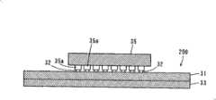
图9是具备金属层的以往的COF基板的示意的截面图。在图9的COF基板200中,在绝缘层31的一个面上设置有多个导体图案32,在另一个面上设置有金属层33。电子产品35的凸部35a被结合在多个导体图案32的端子部上。通过这种结构,电子部件35的热通过金属层33被发散。9 is a schematic cross-sectional view of a conventional COF substrate provided with a metal layer. In the
但是,在安装电子部件35时,需要确认电子部件35相对于多个导体图案32是否没有位置偏移。在COF基板200上未设置金属层33的情况下,能够从绝缘层31的另一个面一侧通过绝缘层31确认电子部件35是否有错位。但是,在设置有金属层33的情况下,难以确认电子部件35的错位。However, when mounting the
发明内容Contents of the invention
本发明的目的在于,提供一种能够提高散热性,并能够容易地确认电子部件的错位的配线电路基板及其制造方法。An object of the present invention is to provide a printed circuit board capable of improving heat dissipation and allowing easy confirmation of misalignment of electronic components, and a method of manufacturing the same.
(1)本发明的一个方面的配线电路基板为具有用于安装电子部件的安装区域的配线电路基板,该配线电路基板包括:绝缘层;形成在绝缘层的一个面上且具有将要与电子部件电连接的端子部的导体图案;和形成在绝缘层的另一个面上且具有开口部的金属层。开口部形成于夹着绝缘层与导体图案的端子部相对的金属层的区域。(1) A printed circuit board according to one aspect of the present invention is a printed circuit board having a mounting area for mounting electronic components, and the printed circuit board includes: an insulating layer; a conductor pattern of a terminal portion electrically connected to the electronic component; and a metal layer formed on the other surface of the insulating layer and having an opening. The opening is formed in a region of the metal layer facing the terminal portion of the conductor pattern with the insulating layer interposed therebetween.
在该配线电路基板中,电子部件与形成在绝缘层的一个面上的导体图案的端子部连接。电子部件的热通过形成在绝缘层的另一个面上的金属层被发散。由此,能够防止电子部件发生误动作。In this printed circuit board, electronic components are connected to the terminal portion of the conductor pattern formed on one surface of the insulating layer. The heat of the electronic component is dissipated through the metal layer formed on the other side of the insulating layer. Thereby, malfunction of an electronic component can be prevented.
在连接电子部件和导体图案时,能够从形成在金属层上的开口部通过绝缘层目视确认导体图案的位置和电子部件的位置。由此,能够容易地确认电子部件相对于导体图案是否存在错位。其结果是,能够提高导体图案和电子部件的连接性,并能够高效迅速地进行电子部件的安装作业。When connecting the electronic component and the conductive pattern, the position of the conductive pattern and the position of the electronic component can be visually confirmed through the insulating layer from the opening formed in the metal layer. Thereby, it is possible to easily confirm whether or not the electronic component is misaligned with respect to the conductor pattern. As a result, the connectivity between the conductor pattern and the electronic component can be improved, and the mounting work of the electronic component can be performed efficiently and quickly.
(2)也可以为以下方式:安装区域具有矩形形状,导体图案包括与安装区域的一边垂直地交叉并从安装区域的内侧向外侧延伸的多个第一导体图案、和与安装区域的另一边垂直地交叉并从安装区域的内侧向外侧延伸的多个第二导体图案,其中,该另一边与安装区域的一边垂直,端子部包括设置于安装区域的内侧的多个第一导体图案的一端上的多个第一端子部、和设置于安装区域的内侧的多个第二导体图案的一端上的多个第二端子部,开口部包括在与多个第一端子部中的至少一个相对的金属层的区域形成的第一开口部、和在与多个第二端子部中的至少一个相对的金属层的区域形成的第二开口部。(2) It is also possible that the installation area has a rectangular shape, and the conductor pattern includes a plurality of first conductor patterns perpendicular to one side of the installation area and extending from the inside to the outside of the installation area, and the other side of the installation area. A plurality of second conductor patterns vertically intersecting and extending from the inside to the outside of the installation area, wherein the other side is perpendicular to one side of the installation area, and the terminal portion includes one end of the plurality of first conductor patterns disposed on the inside of the installation area A plurality of first terminal portions on the mounting area, and a plurality of second terminal portions disposed on one end of the plurality of second conductor patterns inside the mounting area, and the opening portion is included opposite to at least one of the plurality of first terminal portions. A first opening formed in a region of the metal layer, and a second opening formed in a region of the metal layer facing at least one of the plurality of second terminal portions.
在此情况下,通过金属层的第一开口部确认第一导体图案的第一端子部和电子部件的位置关系,由此,能够确认与安装区域的一边平行的方向上的电子部件有无错位。In this case, by checking the positional relationship between the first terminal portion of the first conductor pattern and the electronic component through the first opening of the metal layer, it is possible to check whether or not the electronic component is misaligned in a direction parallel to one side of the mounting region. .
此外,通过金属层的第二开口部确认第二导体图案的第二端子部和电子部件的位置关系,由此,能够确认与安装区域的另一边平行的方向上的电子部件有无错位。进一步,根据第一或第二端子部与电子 部件的位置关系,能够确认电子部件是否存在倾斜。In addition, by checking the positional relationship between the second terminal portion of the second conductor pattern and the electronic component through the second opening of the metal layer, it is possible to check whether or not the electronic component is misaligned in a direction parallel to the other side of the mounting region. Further, according to the positional relationship between the first or second terminal portion and the electronic component, it can be confirmed whether the electronic component is tilted.
由此,能够不令结构复杂化地正确地确认电子部件的错位。Thereby, the displacement of an electronic component can be confirmed accurately, without complicating a structure.
(3)本发明的另一方面的配线电路基板的制造方法为具有用于安装电子部件的安装区域的配线电路基板的制造方法,该配线电路基板的制造方法包括:在绝缘层的一个面上形成具有将要与电子部件电连接的端子部的导体图案的工序;和在绝缘层的另一个面上形成具有开口部的金属层的工序,开口部形成于夹着绝缘层与导体图案的端子部相对的金属层的区域。(3) A method of manufacturing a printed circuit board according to another aspect of the present invention is a method of manufacturing a printed circuit board having a mounting area for mounting electronic components, and the method of manufacturing the printed circuit board includes: A process of forming a conductor pattern having a terminal portion to be electrically connected to an electronic component on one surface; and a process of forming a metal layer having an opening on the other surface of the insulating layer, and the opening is formed between the insulating layer and the conductor pattern. area of the metal layer opposite the terminal portion.
在该配线电路基板的制造方法中,在绝缘层的一个面上形成导体图案,在绝缘层的另一个面上形成金属层。在此情况下,与导体图案连接的电子部件的热通过金属层被发散。由此,能够防止电子部件发生误动作。In this method of manufacturing a printed circuit board, a conductive pattern is formed on one surface of the insulating layer, and a metal layer is formed on the other surface of the insulating layer. In this case, the heat of the electronic component connected to the conductor pattern is dissipated through the metal layer. Thereby, malfunction of an electronic component can be prevented.
此外,在连接电子部件和导体图案时,能够从形成在金属层上的开口部通过绝缘层目视确认导体图案的位置和电子部件的位置。由此,能够容易地确认电子部件相对于导体图案是否存在错位。其结果是,能够提高导体图案和电子部件的连接性,并能够高效迅速地进行电子部件的安装作业。In addition, when the electronic component and the conductive pattern are connected, the position of the conductive pattern and the position of the electronic component can be visually confirmed through the insulating layer from the opening formed in the metal layer. Thereby, it is possible to easily confirm whether or not the electronic component is misaligned with respect to the conductor pattern. As a result, the connectivity between the conductor pattern and the electronic component can be improved, and the mounting work of the electronic component can be performed efficiently and quickly.
根据本发明,电子部件的热通过形成在绝缘层的另一个面上的金属层被发散。由此,能够防止电子部件发生误动作。此外,能够从形成于金属层上的开口部通过绝缘层目视确认导体图案的位置和电子部件的位置。由此,能够容易地确认电子部件相对于导体图案是否存在错位。According to the present invention, the heat of the electronic component is dissipated through the metal layer formed on the other side of the insulating layer. Thereby, malfunction of an electronic component can be prevented. In addition, the position of the conductor pattern and the position of the electronic component can be visually confirmed through the insulating layer from the opening formed in the metal layer. Thereby, it is possible to easily confirm whether or not the electronic component is misaligned with respect to the conductor pattern.
附图说明Description of drawings
图1是本实施方式的COF基板的截面图。FIG. 1 is a cross-sectional view of a COF substrate according to this embodiment.
图2是本实施方式的COF基板的平面图。FIG. 2 is a plan view of the COF substrate of the present embodiment.
图3是表示通过开口部看到的导体图案的端子部和电子部件的凸部的图。FIG. 3 is a view showing a terminal portion of a conductor pattern and a convex portion of an electronic component seen through an opening.
图4是通过开口部看到的导体图案的端子部和电子部件的凸部的部分放大图。4 is a partially enlarged view of a terminal portion of a conductor pattern and a convex portion of an electronic component seen through an opening.
图5是通过开口部看到的导体图案的端子部和电子部件的凸部的 部分放大图。Fig. 5 is a partially enlarged view of a terminal portion of a conductor pattern and a convex portion of an electronic component seen through an opening.
图6是用于对本实施方式的COF基板的制造方法进行说明的工序截面图。FIG. 6 is a process cross-sectional view for explaining the method of manufacturing the COF substrate of the present embodiment.
图7是用于对本实施方式的COF基板的制造方法进行说明的工序截面图。FIG. 7 is a cross-sectional view illustrating steps of a method of manufacturing a COF substrate according to the present embodiment.
图8是用于说明电子部件的安装作业的示意图。FIG. 8 is a schematic diagram for explaining mounting work of electronic components.
图9是设置有金属层的以往的COF基板的示意的截面图。9 is a schematic cross-sectional view of a conventional COF substrate provided with a metal layer.
具体实施方式Detailed ways
以下,参照附图,对本发明的一个实施方式的配线电路基板及其制造方法进行说明。而且,在本实施方式中,作为配线电路基板的一例,对COF(chip on film)用的基板(以下称为COF基板)进行说明。Hereinafter, a printed circuit board and a method of manufacturing the same according to an embodiment of the present invention will be described with reference to the drawings. In addition, in this embodiment, a substrate for COF (chip on film) (hereinafter referred to as a COF substrate) will be described as an example of a printed circuit board.
(1)结构(1) Structure
图1为本实施方式的COF基板的截面图,图2为本实施方式的COF基板的平面图。其中,图2(a)表示图1中的COF基板的上表面,图2(b)表示图1中的COF基板的下表面。此外,图2(a)和图2(b)的A-A线截面相当于图1的截面。FIG. 1 is a cross-sectional view of the COF substrate of the present embodiment, and FIG. 2 is a plan view of the COF substrate of the present embodiment. 2( a ) shows the upper surface of the COF substrate in FIG. 1 , and FIG. 2( b ) shows the lower surface of the COF substrate in FIG. 1 . In addition, the A-A line cross section of FIG. 2( a ) and FIG. 2( b ) corresponds to the cross section of FIG. 1 .
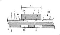
如图1和图2所示,COF基板100具有例如由聚酰亚胺构成的绝缘层1。在绝缘层1的一个面的大致中央部,设置有长方形状的安装区域S。多个导体图案2形成为从安装区域S的内侧向外侧延伸。As shown in FIGS. 1 and 2 , a
在各导体图案2的前端设置有端子部21。多个端子部21在安装区域S的内侧沿着安装区域S的一对长边和一对短边配置。多个导体图案2与安装区域S的一对长边和一对短边垂直地交叉并延伸。而且,多个导体图案2包括用于传送电信号或电力的配线图案、和不传输电信号或电力的虚载(dummy:ダミ一)图案。在安装区域S的周围,以覆盖多个导体图案2的方式形成盖绝缘层4。A
以与安装区域S重叠的方式,在绝缘层1上安装电子部件5(例如LSI(Large scale integration:大规模集成电路)。具体而言,电子部件5的多个凸部5a(图1)结合在多个导体图案2的端子部21上。安装区域S的形状设定为与平面视野上(平面观察时)的电子部件5的形状相同。即,在本示例中使用长方形的电子部件5。多个凸部5a以与 多个端子部21对应的方式沿着电子部件5的一对长边或一对短边设置。Electronic components 5 (such as LSI (Large scale integration: Large Scale Integration)) are mounted on the insulating
如图2(b)所示,在绝缘层1的另一个面上设置有例如由铜构成的金属层3。在此情况下,电子部件5产生的热经由绝缘层1被传导至金属层3并被发散。因此,由于热不会滞留在电子部件5及其周围,所以能够防止电子部件5发生误动作。As shown in FIG. 2( b ), a
在金属层3上,沿着安装区域S的一对长边和一对短边形成有矩形的开口部3a~3f。在本示例中,沿着安装区域S的一个长边形成有开口部3a、3b,沿着另一个长边形成有开口部3c、3d。此外,沿着安装区域的一个短边形成有开口部3e,沿着另一个短边形成有开口部3f。开口部3a~3f夹着绝缘层1分别与多个导体图案2的端子部21的一部分相对。On the
(2)开口部(2) Opening
在本实施方式的COF基板100中,能够通过形成在金属层3上的开口部3a~3f确认电子部件5有无错位。使用3和图4进行详细说明。In the
图3(a)是表示通过图2(b)的开口部3a看到的导体图案2的端子部21和电子部件5的凸部5a的图,图3(b)是表示通过图2(b)的开口部3e看到的导体图案2的端子部21和电子部件5的凸部5a的图。Fig. 3 (a) is a diagram showing the
如图3(a)和图3(b)所示,通过开口部3a、3e,能够目视确认导体图案2的端子部21的位置和电子部件5的凸部5a的位置。由此,能够容易且迅速地确认电子部件5的各凸部5a是否与对应的导体图案2的端子部21被正确地连接。As shown in FIG. 3( a ) and FIG. 3( b ), the position of the
接着,参照图4和图5,对电子部件5的错位的确认方法进行具体的说明。在图4(a)和图5(a)中,部分地放大表示通过开口部3a看到的导体图案2的端子部21和电子部件5的凸部5a,在图4(b)和图5(b)中,部分地放大表示通过开口部3e看到的导体图案2的端子部21和电子部件5的凸部5a。Next, the method of confirming the displacement of the
如图4(a)所示,在通过开口部3a观察的情况下,根据凸部5a的中心线L1与端子部21的中心线L2是否一致,能够确认电子部件5的横方向(图中的R1方向)的错位。在通过开口部3a观察的情况下,如果凸部5a的中心线L1与端子部21的中心线L2一致,则电子部件5在横方向不存在错位。As shown in Figure 4 (a), under the situation of observing through the
此外,如图4(b)所示,在通过开口部3e观看的情况下,根据凸部5a的中心线L1与端子部21的中心线L2是否一致,能够确认电子部件5的纵方向(图中的R2方向)的错位。在通过开口部3e观看的情况下,如果凸部5a的中心线L1与端子部21的中心线L2一致,则电子部件5在纵方向不存在错位。In addition, as shown in Figure 4 (b), in the case of viewing through the
此外,如图5(a)和图5(b)所示,根据凸部5a的一边与端子部21的一边是否平行,能够确认电子部件5的旋转方向的错位。如果凸部5a的一边与端子部21的一边平行(如果图5(a)和图5(b)的角度θ为0),则电子部件5在旋转方向上不存在错位。In addition, as shown in FIG. 5( a ) and FIG. 5( b ), it is possible to confirm the displacement of the rotation direction of the
如果电子部件5在横方向、纵方向和旋转方向上均不存在偏差,则电子部件5已被正确地安装在COF基板100上。另一方面,如果电子部件5在纵方向、横方向和旋转方向的任一方向上存在错位,则电子部件5存在错位。If there is no deviation of the
此外,在图2(b)的示例中,沿着安装区域S的一对长边设置有开口部3a~3d,沿着一对短边形成有开口部3e、3f,但是如果能够确认电子部件5的纵方向、横方向和旋转方向的错位,也可以沿着安装区域S的一对长边中的任意一边设置一个开口部,沿着安装区域S的一对短边中的任意一边设置一个开口部。例如,也可以只设置开口部3a~3d中的任意一个,只设置开口部3e、3f中的任意一个。In addition, in the example of FIG. 2(b), the
但是,为了能够正确地确认电子部件5的纵方向、横方向和旋转方向的错位,优选至少沿着安装区域S的一个长边和另一个长边,相对于安装区域S的中心部对称地设置两个开口部,沿着安装区域S的一对短边中的任意一边设置一个开口部。例如,设置开口部3a~3d中的开口部3a、3d或开口部3b、3c,设置开口部3e、3f中的任意一个。However, in order to accurately confirm the misalignment of the vertical direction, the lateral direction and the rotation direction of the
开口部3a~3f的形状不限于矩形,还可以为三角形或者圆形等其它形状。此外,也可以任意地设定开口部3a~3f的大小,例如还可以沿着安装区域S的长边或短边设置缝隙状的开口部。The shape of the
此外,还可以按照导体图案2的配置等,适当改变金属层3的开口部的形状和配置等。In addition, the shape and arrangement of the openings of the
(3)制造方法(3) Manufacturing method
接着,对本实施方式的COF基板100的制造方法的一例进行说明。图6和图7是用于对本实施方式的COF基板100的制造方法进行说明的工序截面图。其中,图6和图7所示的截面相当于图2的B-B线截面。Next, an example of a method for manufacturing the
如图6(a)所示,准备由聚酰亚胺和铜构成的双层基材。该双层基材相当于COF基板100的绝缘层1和金属层3。As shown in FIG. 6( a ), a two-layer substrate composed of polyimide and copper was prepared. This double-layer substrate corresponds to the insulating
首先,在绝缘层1的上表面上通过溅射形成金属薄膜(未图示)。然后,如图6(b)所示,在金属薄膜上形成具有多个导体图案2(图1)的反转图案(reverse pattern)的干膜抗蚀剂(dry film resist)12。多个反转图案通过对干膜抗蚀剂12进行曝光和显像而形成。First, a metal thin film (not shown) is formed by sputtering on the upper surface of insulating
接着,如图6(c)所示,在绝缘层1的露出部分(金属薄膜的露出部分)上通过电解电镀形成多个导体图案2。然后,如图6(d)所示,利用剥离液除去干膜抗蚀剂12,并通过蚀刻除去干膜抗蚀剂12下的金属薄膜的区域。Next, as shown in FIG. 6(c), a plurality of
接着,作为用于实现与电子部件5连接的表面处理,在导体图案2的表面进行锡的无电解电镀。之后,如图7(e)所示,以覆盖导体图案2的规定的区域的方式形成盖绝缘层4。Next, electroless tin plating is performed on the surface of the
接着,如图7(f)所示,除了形成开口部3a~3f的区域,在金属层的下表面上形成干膜抗蚀剂13。然后,如图7(g)所示,对露出的金属层3的部分进行蚀刻,形成开口部3a~3f。而后,如图7(h)所示,通过剥离液除去干膜抗蚀剂13。这样,完成本实施方式的COF基板100。Next, as shown in FIG. 7( f ), dry film resist 13 is formed on the lower surface of the metal layer except for the region where
而且,在此对通过半加成法(semi-additive)形成导体图案2的例子进行了说明,但也可以通过消减(subtractive)法形成导体图案2。Furthermore, an example in which the
(4)实施例和比较例(4) Examples and Comparative Examples
(4-1)实施例(4-1) Example
以下述条件制造成COF基板100。The
作为绝缘层1的材料使用聚酰亚胺,作为导体图案2和金属层3的材料使用铜。此外,令绝缘层1的厚度为35μm,金属层3的厚度为15μm。此外,令导体图案2的端子部21的宽度为8μm,相邻的 端子部21间的间隔为12μm。此外,在金属层3上形成正方形的开口部3a~3f。令开口部3a~3f的一边的长度为100μm。此外,电子部件5的凸部5a的尺寸为13μm×75μm。Polyimide was used as a material for insulating
(4-2)比较例(4-2) Comparative example
除了在金属层3上不形成开口部3a~3f以外,与上述实施例相同地制造COF基板100。The
(4-3)评价(4-3) Evaluation
以下述条件进行电子部件5的安装作业。The mounting work of the
图8是用于说明电子部件5的安装作业的示意图。如图8所示,多个COF基板100以延伸为较长形状的方式被一体地形成,并沿着方向T1被搬运。在安装部M1,在载物台11上载置有一个COF基板100。在此状态下,工具12通过热压接将电子部件5安装在载物台11上的COF基板100上。而且,令安装时的工具12的温度为430℃,载物台11的温度为100℃,安装负载为30N。FIG. 8 is a schematic diagram for explaining the mounting operation of the
在安装电子部件5之后,使用CCD照相机13从金属层3一侧(下表面一侧)观察COF基板100。After the
其结果是,在实施例中,通过金属层3的开口部3a~3f能够容易地确认电子部件5的错位。因此,能够高效迅速地进行电子部件5的安装作业。另一方面,在比较例中,难以确认电子部件5的错位。因此,大幅度降低了电子部件5的安装作业的效率。As a result, in the example, the dislocation of the
(5)发明内容的各构成要素与实施方式的各要素的对应(5) Correspondence between each constituent element of the content of the invention and each element of the embodiment
以下,对于发明内容的各构成要素与实施方式的各要素的对应的示例进行说明,但本发明不限于下述示例。Hereinafter, an example of correspondence between each constituent element of the summary of the invention and each element of the embodiment will be described, but the present invention is not limited to the following example.
在上述实施方式中,COF基板100为配线电路基板的示例,安装区域的长边为安装区域的一边的示例,安装区域的短边为安装区域的另一边的示例。此外,与安装区域的长边交叉的导体图案2为第一导体图案的示例,沿着安装区域的长边配置的端子部21为第一端子部的示例,与安装区域的短边交叉的导体图案2为第二导体图案的示例,沿着安装区域的短边配置的端子部21为第二端子部的示例。此外,开口部3a~3f为第一开口部的示例,开口部3e、3f为第二开口部的示例。In the above embodiments, the
作为发明内容的各构成要素,还能够使用具有发明内容所述的结 构或者功能的其它各种要素。As each constituent element of the summary of the invention, other various elements having the configuration or function described in the summary of the invention can also be used.
(6)其它实施方式(6) Other implementations
绝缘层1的材料不限于聚酰亚胺,还可以使用聚对苯二甲酸乙二酯、聚醚腈、聚醚砜等其它绝缘材料。此外,导体图案2的材料不限于铜,还可以使用铜合金、金、铝等其它金属材料。The material of the insulating
金属层3的材料不限于铜。但是,优选使用铜、金、银或铝等导热率高的金属。The material of the
本发明能够应用于柔性配线电路基板、硬性(rigid)配线电路基板等各种配线电路基板。此外,作为电子部件5,不限于LSI,还可以使用电容器等其它电子部件。The present invention can be applied to various printed circuit boards such as flexible printed circuit boards and rigid printed circuit boards. In addition, as the
Claims (3)
Applications Claiming Priority (3)
| Application Number | Priority Date | Filing Date | Title |
|---|---|---|---|
| JP2008021274AJP5238274B2 (en) | 2008-01-31 | 2008-01-31 | Wiring circuit board and manufacturing method thereof |
| JP2008-021274 | 2008-01-31 | ||
| JP2008021274 | 2008-01-31 |
Publications (2)
| Publication Number | Publication Date |
|---|---|
| CN101499453A CN101499453A (en) | 2009-08-05 |
| CN101499453Btrue CN101499453B (en) | 2012-05-16 |
Family
ID=40637854
Family Applications (1)
| Application Number | Title | Priority Date | Filing Date |
|---|---|---|---|
| CN2009100019740AExpired - Fee RelatedCN101499453B (en) | 2008-01-31 | 2009-01-24 | Printed circuit board and method of manufacturing the same |
Country Status (7)
| Country | Link |
|---|---|
| US (1) | US8102664B2 (en) |
| EP (1) | EP2086296B1 (en) |
| JP (1) | JP5238274B2 (en) |
| KR (1) | KR101477818B1 (en) |
| CN (1) | CN101499453B (en) |
| AT (1) | ATE536087T1 (en) |
| TW (1) | TWI453870B (en) |
Families Citing this family (6)
| Publication number | Priority date | Publication date | Assignee | Title |
|---|---|---|---|---|
| JP5528250B2 (en) | 2010-07-30 | 2014-06-25 | 日東電工株式会社 | Method for manufacturing printed circuit board |
| JP5829139B2 (en) | 2012-02-03 | 2015-12-09 | 日東電工株式会社 | WIRING CIRCUIT BOARD, ITS MANUFACTURING METHOD, AND CONNECTION TERMINAL |
| JP6452001B2 (en)* | 2016-06-08 | 2019-01-16 | 株式会社村田製作所 | Electronic device and method for manufacturing electronic device |
| JP6745712B2 (en)* | 2016-11-30 | 2020-08-26 | 日東電工株式会社 | Wiring circuit board and manufacturing method thereof |
| JP7016147B2 (en)* | 2017-11-29 | 2022-02-04 | 深▲セン▼通鋭微電子技術有限公司 | Chip-on-film semiconductor device |
| KR102430750B1 (en)* | 2019-08-22 | 2022-08-08 | 스템코 주식회사 | Circuit board and method for manufacturing the same |
Citations (4)
| Publication number | Priority date | Publication date | Assignee | Title |
|---|---|---|---|---|
| CN1767177A (en)* | 2004-10-05 | 2006-05-03 | 夏普株式会社 | Semiconductor devices and electronic equipment |
| CN1873959A (en)* | 2005-06-03 | 2006-12-06 | 三星电子株式会社 | Driver ic package with improved heat dissipation |
| CN1901179A (en)* | 2005-07-18 | 2007-01-24 | 三星电子株式会社 | Tape wiring substrate and chip-on-film package using the same |
| CN1967831A (en)* | 2005-11-14 | 2007-05-23 | 日东电工株式会社 | Wired circuit board and method for manufacturing wired circuit board and mounting electronic component thereon |
Family Cites Families (7)
| Publication number | Priority date | Publication date | Assignee | Title |
|---|---|---|---|---|
| JP2875076B2 (en)* | 1990-11-29 | 1999-03-24 | 三井化学株式会社 | Flexible wiring board |
| JP2808952B2 (en) | 1991-11-27 | 1998-10-08 | 日立電線株式会社 | Substrate for mounting semiconductor elements |
| JP3549294B2 (en)* | 1995-08-23 | 2004-08-04 | 新光電気工業株式会社 | Semiconductor device and its mounting structure |
| JP2000347207A (en)* | 1999-06-04 | 2000-12-15 | Nec Corp | Liquid crystal display device and production of liquid crystal display device |
| JP2001007460A (en) | 1999-06-17 | 2001-01-12 | Iwaki Denshi Kk | Recognition mark structure for flexible substrate |
| JP3866058B2 (en)* | 2001-07-05 | 2007-01-10 | シャープ株式会社 | Semiconductor device, wiring board and tape carrier |
| JP4779826B2 (en)* | 2006-06-29 | 2011-09-28 | パナソニック株式会社 | Flexible printed circuit board |
- 2008
- 2008-01-31JPJP2008021274Apatent/JP5238274B2/enactiveActive
- 2008-12-08TWTW097147650Apatent/TWI453870B/ennot_activeIP Right Cessation
- 2009
- 2009-01-07ATAT09250027Tpatent/ATE536087T1/enactive
- 2009-01-07EPEP09250027Apatent/EP2086296B1/ennot_activeNot-in-force
- 2009-01-22USUS12/357,714patent/US8102664B2/ennot_activeExpired - Fee Related
- 2009-01-24CNCN2009100019740Apatent/CN101499453B/ennot_activeExpired - Fee Related
- 2009-01-29KRKR1020090006894Apatent/KR101477818B1/ennot_activeExpired - Fee Related
Patent Citations (4)
| Publication number | Priority date | Publication date | Assignee | Title |
|---|---|---|---|---|
| CN1767177A (en)* | 2004-10-05 | 2006-05-03 | 夏普株式会社 | Semiconductor devices and electronic equipment |
| CN1873959A (en)* | 2005-06-03 | 2006-12-06 | 三星电子株式会社 | Driver ic package with improved heat dissipation |
| CN1901179A (en)* | 2005-07-18 | 2007-01-24 | 三星电子株式会社 | Tape wiring substrate and chip-on-film package using the same |
| CN1967831A (en)* | 2005-11-14 | 2007-05-23 | 日东电工株式会社 | Wired circuit board and method for manufacturing wired circuit board and mounting electronic component thereon |
Also Published As
| Publication number | Publication date |
|---|---|
| JP5238274B2 (en) | 2013-07-17 |
| US8102664B2 (en) | 2012-01-24 |
| KR101477818B1 (en) | 2014-12-30 |
| EP2086296A3 (en) | 2010-05-26 |
| KR20090084706A (en) | 2009-08-05 |
| US20090195998A1 (en) | 2009-08-06 |
| ATE536087T1 (en) | 2011-12-15 |
| CN101499453A (en) | 2009-08-05 |
| TWI453870B (en) | 2014-09-21 |
| JP2009182229A (en) | 2009-08-13 |
| EP2086296A2 (en) | 2009-08-05 |
| TW200947635A (en) | 2009-11-16 |
| EP2086296B1 (en) | 2011-11-30 |
Similar Documents
| Publication | Publication Date | Title |
|---|---|---|
| KR102375126B1 (en) | Flexible circuit board and chip pakage comprising the same, and electronic device comprising the same | |
| JP2004343030A (en) | Wiring circuit board, manufacturing method thereof, circuit module provided with this wiring circuit board | |
| JP5788166B2 (en) | Connection terminal structure, manufacturing method thereof, and socket | |
| JP2008060526A (en) | Chip film package and display panel assembly including the same | |
| CN101499453B (en) | Printed circuit board and method of manufacturing the same | |
| JP2005079581A (en) | Tape substrate, semiconductor chip package using the tape substrate, and LCD device using the semiconductor chip package | |
| JP2010277829A (en) | Substrate having connection terminal | |
| EP2086297B1 (en) | Printed circuit board and method of manufacturing the same | |
| CN1941353A (en) | Circuit board, and semiconductor device | |
| KR101139084B1 (en) | Multilayer printed circuit board and method of making same | |
| EP2086295B1 (en) | Printed circuit board and method of manufacturing the same | |
| US6853080B2 (en) | Electronic device and method of manufacturing the same, and electronic instrument | |
| JP3977072B2 (en) | Wiring board, semiconductor device, and manufacturing method thereof | |
| JP4488073B2 (en) | Electrical connection device | |
| JP2005340294A (en) | WIRING BOARD AND ITS MANUFACTURING METHOD, SEMICONDUCTOR DEVICE AND ITS MANUFACTURING METHOD, ELECTRONIC DEVICE, AND ELECTRONIC DEVICE | |
| US7122909B2 (en) | Wiring board, stacked wiring board and method of manufacturing the same, semiconductor device and method of manufacturing the same, circuit board, and electronic instrument | |
| JP2006339276A (en) | Substrate for connection and manufacturing method thereof | |
| JP3714388B2 (en) | SEMICONDUCTOR DEVICE AND ITS MANUFACTURING METHOD, WIRING BOARD, CIRCUIT BOARD AND ELECTRONIC DEVICE | |
| JP4388168B2 (en) | Resin molded substrate | |
| JP2004228353A (en) | Wiring board and manufacturing method thereof, laminated wiring board, semiconductor device, circuit board, and electronic equipment | |
| JP4123371B2 (en) | Semiconductor device and manufacturing method thereof, circuit board, and electronic apparatus | |
| JP2012114312A (en) | Tape carrier for semiconductor device | |
| JP2008124107A (en) | Wiring board, semiconductor component, and manufacturing method of wiring board | |
| JP2005101171A (en) | SEMICONDUCTOR DEVICE AND ITS MANUFACTURING METHOD, WIRING BOARD, CIRCUIT BOARD AND ELECTRONIC DEVICE | |
| JP2006332114A (en) | Connection substrate, semiconductor device, and process for producing connection substrate |
Legal Events
| Date | Code | Title | Description |
|---|---|---|---|
| C06 | Publication | ||
| PB01 | Publication | ||
| C10 | Entry into substantive examination | ||
| SE01 | Entry into force of request for substantive examination | ||
| C14 | Grant of patent or utility model | ||
| GR01 | Patent grant | ||
| CF01 | Termination of patent right due to non-payment of annual fee | Granted publication date:20120516 | |
| CF01 | Termination of patent right due to non-payment of annual fee |