CN101496186B - LED light source with hollow collecting lens - Google Patents
LED light source with hollow collecting lensDownload PDFInfo
- Publication number
- CN101496186B CN101496186BCN2007800284995ACN200780028499ACN101496186BCN 101496186 BCN101496186 BCN 101496186BCN 2007800284995 ACN2007800284995 ACN 2007800284995ACN 200780028499 ACN200780028499 ACN 200780028499ACN 101496186 BCN101496186 BCN 101496186B
- Authority
- CN
- China
- Prior art keywords
- led
- light
- lens
- light source
- virtual image
- Prior art date
- Legal status (The legal status is an assumption and is not a legal conclusion. Google has not performed a legal analysis and makes no representation as to the accuracy of the status listed.)
- Expired - Fee Related
Links
Images


Classifications
- H—ELECTRICITY
- H10—SEMICONDUCTOR DEVICES; ELECTRIC SOLID-STATE DEVICES NOT OTHERWISE PROVIDED FOR
- H10H—INORGANIC LIGHT-EMITTING SEMICONDUCTOR DEVICES HAVING POTENTIAL BARRIERS
- H10H20/00—Individual inorganic light-emitting semiconductor devices having potential barriers, e.g. light-emitting diodes [LED]
- H10H20/80—Constructional details
- H10H20/85—Packages
- H10H20/855—Optical field-shaping means, e.g. lenses
- G—PHYSICS
- G02—OPTICS
- G02B—OPTICAL ELEMENTS, SYSTEMS OR APPARATUS
- G02B19/00—Condensers, e.g. light collectors or similar non-imaging optics
- G02B19/0004—Condensers, e.g. light collectors or similar non-imaging optics characterised by the optical means employed
- G02B19/0009—Condensers, e.g. light collectors or similar non-imaging optics characterised by the optical means employed having refractive surfaces only
- G02B19/0014—Condensers, e.g. light collectors or similar non-imaging optics characterised by the optical means employed having refractive surfaces only at least one surface having optical power
- G—PHYSICS
- G02—OPTICS
- G02B—OPTICAL ELEMENTS, SYSTEMS OR APPARATUS
- G02B19/00—Condensers, e.g. light collectors or similar non-imaging optics
- G02B19/0033—Condensers, e.g. light collectors or similar non-imaging optics characterised by the use
- G02B19/0047—Condensers, e.g. light collectors or similar non-imaging optics characterised by the use for use with a light source
- G02B19/0061—Condensers, e.g. light collectors or similar non-imaging optics characterised by the use for use with a light source the light source comprising a LED
- G—PHYSICS
- G02—OPTICS
- G02B—OPTICAL ELEMENTS, SYSTEMS OR APPARATUS
- G02B3/00—Simple or compound lenses
- G02B3/02—Simple or compound lenses with non-spherical faces
- G02B3/08—Simple or compound lenses with non-spherical faces with discontinuous faces, e.g. Fresnel lens
- H—ELECTRICITY
- H01—ELECTRIC ELEMENTS
- H01L—SEMICONDUCTOR DEVICES NOT COVERED BY CLASS H10
- H01L2224/00—Indexing scheme for arrangements for connecting or disconnecting semiconductor or solid-state bodies and methods related thereto as covered by H01L24/00
- H01L2224/01—Means for bonding being attached to, or being formed on, the surface to be connected, e.g. chip-to-package, die-attach, "first-level" interconnects; Manufacturing methods related thereto
- H01L2224/42—Wire connectors; Manufacturing methods related thereto
- H01L2224/47—Structure, shape, material or disposition of the wire connectors after the connecting process
- H01L2224/48—Structure, shape, material or disposition of the wire connectors after the connecting process of an individual wire connector
- H01L2224/4805—Shape
- H01L2224/4809—Loop shape
- H01L2224/48091—Arched
- Y—GENERAL TAGGING OF NEW TECHNOLOGICAL DEVELOPMENTS; GENERAL TAGGING OF CROSS-SECTIONAL TECHNOLOGIES SPANNING OVER SEVERAL SECTIONS OF THE IPC; TECHNICAL SUBJECTS COVERED BY FORMER USPC CROSS-REFERENCE ART COLLECTIONS [XRACs] AND DIGESTS
- Y10—TECHNICAL SUBJECTS COVERED BY FORMER USPC
- Y10S—TECHNICAL SUBJECTS COVERED BY FORMER USPC CROSS-REFERENCE ART COLLECTIONS [XRACs] AND DIGESTS
- Y10S362/00—Illumination
- Y10S362/80—Light emitting diode
Landscapes
- Physics & Mathematics (AREA)
- General Physics & Mathematics (AREA)
- Optics & Photonics (AREA)
- Led Device Packages (AREA)
- Non-Portable Lighting Devices Or Systems Thereof (AREA)
- Lenses (AREA)
Abstract
Description
Translated fromChinese相关专利申请的交叉引用Cross references to related patent applications
本专利申请基于并要求2006年7月31提交的美国临时专利申请序号60/820887的优先权,其内容据此全文引入以供参考。This patent application is based upon and claims the benefit of priority from US Provisional Patent Application Serial No. 60/820887, filed July 31, 2006, the contents of which are hereby incorporated by reference in their entirety.
参考内容有:同此提交于同一天的名称为“LED Mosaic”(代理人案卷号62370US006)的共同转让的美国专利申请;2005年12月30日提交的并且作为美国专利申请公开US2007/0152231公开的名称为“LED With Compound Encapsulant Lens”(具有化合物封壳透镜的LED)的美国专利申请序号11/322,801;于此提交于同一天的名称为“Optical Projection Subsystem”(光学投影子系统)(代理人案卷号63281US002)的美国专利申请;提交于2007年7月2日的名称为“LEDIllumination System With Polarization Recycling”(具有偏振回收利用的LED照明系统)的美国专利申请序号11/772,609;同此提交于同一天的名称为“Combination Camera/Projector System”(结合相机/投影系统)(代理人案卷号62369US006)的美国专利申请;同此提交于同一天的名称为“Integrating Light Source Module”(集成光源模块)(代理人案卷号62382US008)的美国专利申请;以及美国专利申请公开US2006/0091411(Ouderkirk等人)“High Brightness LED Package”(高亮度LED包)、US2006/0091798(Ouderkirk等人)“High Brightness LEDPackage With Compound Optical Element(s)”(具有化合物光学元件的高亮度LED包)和US2006/0092532(Ouderkirk等人)“HighBrightness LED Package With Multiple Optical Elements”(具有多个光学元件的高亮度LED包)。References are: commonly assigned U.S. Patent Application entitled "LED Mosaic" (Attorney Docket No. 62370US006), filed on the same date herewith; U.S. Patent Application Serial No. 11/322,801, entitled "LED With Compound Encapsulant Lens"; filed hereon on the same day as "Optical Projection Subsystem" (Attorney Docket No. 63281US002); U.S. Patent Application Serial No. 11/772,609, filed July 2, 2007, entitled "LED Illumination System With Polarization Recycling"; hereby filed U.S. Patent Application entitled "Combination Camera/Projector System" (Attorney Docket No. 62369US006), filed on the same date; Module) (Attorney Docket No. 62382US008); and US Patent Application Publications US2006/0091411 (Ouderkirk et al.) "High Brightness LED Package" (High Brightness LED Package), US2006/0091798 (Ouderkirk et al.) "High Brightness LED Package" Brightness LED Package With Compound Optical Element(s)" and US2006/0092532 (Ouderkirk et al.) "High Brightness LED Package With Multiple Optical Elements" (High Brightness LED Package With Multiple Optical Elements) ).
背景技术Background technique
发光二极管(LED)是光源的理想选择,部分是因为其尺寸相对小、电源/电流要求低、响应时间短、寿命长、稳固的包装、各种可用输出波长以及与现代电路构造的相容性。这些特性有助于解释过去数十年中,它们得以广泛应用于大量不同的最终应用场合的原因。对LED的功效、亮度以及输出波长方面的改进一直在持续进行,这进一步扩大了潜在的最终应用范围。Light-emitting diodes (LEDs) are ideal for light sources, in part because of their relatively small size, low power/current requirements, short response time, long lifetime, robust packaging, wide range of available output wavelengths, and compatibility with modern circuit configurations . These properties help explain their widespread use in a large number of different end applications over the past few decades. Improvements in LED efficacy, brightness, and output wavelength are continuing, further expanding the range of potential end applications.
LED通常打包销售,包装中包括安装在金属接头上的LED晶粒或薄片。所述接头可配有反射杯,杯中装配LED晶粒,电引线连接到LED晶粒。某些封装也包括模制的透明树脂,形成胶囊包封LED晶粒。胶囊包封树脂可以具有在局部使晶粒射出的光保持平行的标称的半球形前表面,或者具有标称的平坦表面。LEDs are usually sold in packages that include LED dies or sheets mounted on metal connectors. The connector may be provided with a reflective cup in which the LED die is fitted and the electrical leads are connected to the LED die. Certain packages also include a molded clear resin that encapsulates the LED die. The encapsulating resin may have a nominally hemispherical front surface that locally keeps the light exiting the die parallel, or a nominally flat surface.
名称为“LED With Compound Encapsulant Lens”(具有化合物封壳透镜的LED)的上述美国专利申请序号11/322,801公开LED光源,所述LED光源包括LED发光体和至少部分地围绕发光体的封壳。所述封壳具有内透镜以及外透镜,所述内透镜的折射率小于所述外透镜的折射率,并且在某些情况下为所述外透镜折射率的约70%到80%。所述内透镜及外透镜可沿着曲面彼此接触,并且在某些情况下所述内透镜基本上是平凸的,并且所述外透镜为凹凸的。内透镜生成发光体的第一虚像,而外透镜生成第二虚像,并且第一虚像位于发光体和第二虚像之间。LED光源能够在紧空间中提供均匀的照明。使用相对的高折射率内侧透镜符合当代教导内容,即通过将其包封在折射率与LED晶粒折射率尽可能接近的介质中提高高折射率LED晶粒或薄片的提取效率。The aforementioned U.S. Patent Application Serial No. 11/322,801, entitled "LED With Compound Encapsulant Lens," discloses an LED light source comprising an LED emitter and an envelope at least partially surrounding the emitter. The capsule has an inner lens and an outer lens, the inner lens having a refractive index less than that of the outer lens, and in some cases about 70% to 80% of the outer lens' refractive index. The inner and outer lenses may contact each other along curved surfaces, and in some cases the inner lens is substantially plano-convex and the outer lens is concave-convex. The inner lens generates a first virtual image of the illuminant, and the outer lens generates a second virtual image, and the first virtual image is positioned between the illuminant and the second virtual image. LED light sources provide even lighting in tight spaces. The use of a relatively high index inner lens is consistent with contemporary teaching to increase the extraction efficiency of high index LED dies or flakes by encapsulating them in a medium with a refractive index as close as possible to that of the LED die.
上述本发明仅提供一般背景技术信息,并非意图用于辅助确定受权利要求书保护的主题范围。The disclosure above provides general background information only and is not intended to be used as an aid in determining the scope of claimed subject matter.
发明内容Contents of the invention
一种光源,包括LED发光体和具有中空腔体的凹凸透镜,在中空腔体中设置LED发光体。凹凸透镜在示例性实施例超半球中,并且它可以生成LED发光体的优质光学图像。透镜的腔体填充有空气,诸如地球大气、惰性气体或真空。A light source includes an LED illuminant and a concave-convex lens with a hollow cavity, and the LED illuminant is arranged in the hollow cavity. A meniscus lens is in the exemplary embodiment hyper-hemispheric, and it can generate a good optical image of the LED illuminant. The cavity of the lens is filled with air, such as the earth's atmosphere, a noble gas or a vacuum.
提供本发明内容从而以简化的形式介绍概念选择,还在以下具体实施方式中进一步描述该概念选择。本发明内容并非意图辨识受权利要求书保护的主题的主要特征或基本特征,也非旨在用于辅助确定受权利要求书保护的主题范围。This Summary is provided to introduce a selection of concepts in a simplified form that are further described below in the Detailed Description. This Summary is not intended to identify key features or essential features of the claimed subject matter, nor is it intended to be used as an aid in determining the scope of the claimed subject matter.
附图说明Description of drawings
图1A是封装的LED光源的图解举例说明。Figure 1A is a schematic illustration of a packaged LED light source.
图1B是具有光提取结构的未封装的LED光源的图解举例说明。Figure IB is a diagrammatic illustration of an unpackaged LED light source with a light extraction structure.
图2是具有中空凹凸集合透镜的LED光源的示意性截面图。Fig. 2 is a schematic cross-sectional view of an LED light source with a hollow meniscus collective lens.
图3是图3中的LED光源的另一个示意性截面图。Fig. 3 is another schematic cross-sectional view of the LED light source in Fig. 3 .
图4示出具有另外光学元件的图2和图3中的光源。Figure 4 shows the light source of Figures 2 and 3 with further optical elements.
图5示出具有另外光学元件图2、图3和图4中的光源。FIG. 5 shows the light source of FIGS. 2 , 3 and 4 with additional optical elements.
图6为分别具有中空凹凸集合透镜和化合物胶囊包封透镜的LED光源之间的焦距比较表。Fig. 6 is a comparison table of focal lengths between LED light sources with hollow concave-convex collective lens and compound encapsulated lens respectively.
图7A和7B是分别具有化合物胶囊包封透镜和中空凹凸集合透镜的LED光源光学布局的示意图。7A and 7B are schematic diagrams of the optical layout of an LED light source with a compound encapsulated lens and a hollow concave-convex collective lens, respectively.
图8是使用本发明所公开的LED光源的投影系统的图解视图。8 is a diagrammatic view of a projection system using the disclosed LED light source.
具体实施方式Detailed ways
本专利申请公开包含在其他内容中的类似于上述引用的‘801专利申请的基于LED的光源,但此处内部透镜被折射率大约为1的空气所取代。就这一点而言,“空气”可以是指地球大气,或任何惰性气体,或甚至真空。通过移除内侧透镜,可将LED发光体设置在透镜(在‘801专利申请中被称为外侧透镜)的中空腔体中,该透镜优选的是超半球型和正凹凸型。该透镜(本文称之为凹凸透镜)捕集几乎完全由LED发光体发射的光的完全半球(2π球面度),并利用基本上为球形的折射表面生成品质相当高的(虚拟)几乎没有失真的发光体图像。This patent application discloses, inter alia, an LED-based light source similar to the above-referenced '801 patent application, but here the inner lens is replaced by air with a refractive index of approximately one. In this regard, "air" may refer to the Earth's atmosphere, or any inert gas, or even a vacuum. By removing the inner lens, the LED emitter can be placed in the hollow cavity of the lens (referred to in the '801 patent application as the outer lens), which is preferably hyper-hemispherical and positive concave-convex. This lens (referred to herein as a meniscus lens) captures a complete hemisphere (2π steradians) almost entirely of the light emitted by the LED emitter and produces a reasonably high-quality (virtual) virtually distortion-free luminous image.
本发明所公开的设计在某些方面与当今教导内容相对立,当今教导内容认为,提高高折射率LED晶粒或薄片提取效率的唯一方式是将其封装在具有最高可用折射率的介质中,即尽可能靠近LED晶粒的折射率。图1A现有技术中示出采用此当今教导内容的LED光源10的基本的例子。LED光源10包括以芯片或薄片的形式设置在金属接头14上的LED发光体12。引线键合16(为简化,只示出一个引线键合)提供至LED发光体12的电气连接。胶囊包封材料18(通常为基于硅树脂的凝胶)包封LED发光体。可用的基于硅树脂的凝胶具有约1.5的折光指数,将提取效率限制到小的百分比。The design disclosed in this invention is in some respects in opposition to today's teaching that the only way to improve the extraction efficiency of a high index LED die or flake is to encapsulate it in a medium with the highest available index of refraction, That is, as close as possible to the refractive index of the LED grain. A basic example of an
如上所述,本发明所公开的实施例脱离了常规的胶囊包封技术,并且反而利用LED发光体和凹凸透镜之间的空气界面。图1B示出在LED发光体12和光源的凹凸透镜之间具有这样的空气界面22的LED光源20的部分。图1B中未示出凹凸透镜,以使得其他可选部件可以更好的示出,但是在本文包含的其他图中示出。在一些实施例中,一个或多个提取结构24连同凹凸透镜一起被形成或布置在LED发光体12上,以帮助耦合从LED晶粒发出的光,因此抑制光在其中的捕集浪费。例如,可通过粗化LED晶粒发射表面或在这样的表面上提供大量晶面或其他结构,诸如次波长结构,来增加从LED晶粒的光提取,即使在没有封壳将其暴露到空气中的情况下也可以这样做。如果封壳的折射率小于具有微结构的LED晶粒的折射率,使用具有光提取微结构的封壳对性能可能是有害的。其他适用提取结构24包括高提取光子晶体结构和线栅提取元件。其他适用提取结构还包括如在美国专利申请出版物US2006/0091411(Ouderkirk等人)“High Brightness LEDPackage”(高亮度LED包装)、US2006/0091798(Ouderkirk等人)“High Brightness LED Package With Compound Optical Element(s)”(具有化合物光学元件的高亮度LED包装),以及US2006/0092532(Ouderkirk等人)“High Brightness LED Package With Multiple OpticalElements”(具有多光学元件的高亮度LED包装)中所公开的玻璃或陶瓷提取器或提取器阵列。利用本文所公开的中空集合(凹凸)透镜技术,提取结构24的用途可以是不干涉这些结构的预期光提取部件。尽管本公开的其他图中未示出提取部件,本文所公开的每个实施例均应理解为可选地涵盖这些部件,虽然该部件并非必须。As noted above, the disclosed embodiments of the present invention depart from conventional encapsulation techniques and instead utilize the air interface between the LED emitter and the meniscus lens. FIG. 1B shows part of an
如本文所用,“发光二极管”或“LED”是指发射光的二极管,不管是可见光、紫外光或红外光。它包括作为“LED”(不论是常规型还是超亮型)销售的各种不同的盒装或封装半导体器件。如果LED发出不可见光(如紫外光),以及在一些发出可见光的情况中,可以将它封装成包括荧光粉(或者它可以照亮设置在远处的荧光粉),以使短波长的光转换为较长波长的光,在某些情况下,还可以得到发射白光的器件。“LED晶粒”是LED最基本的形态,即经半导体加工方法制成的单个元件或芯片。例如,LED晶粒通常是由一种或多种III族元素的组合和一种或多种V族元素组合形成的(III-V半导体)。合适的III-V半导体材料的实例包括氮化物(如氮化镓)和磷化物(如磷化铟镓)。还可以使用其它类型的III-V材料,同样可以使用元素周期表中其它族的无机材料。元件或薄片可以包括适用于应用能量的电触点以给装置提供能量。实例包括引线接合、卷带自动结合(TAB)或芯片倒装焊接。该元件或芯片的各独立层和其它功能元件通常以晶片级形成,并且可将加工好的晶片切成单个元件,以生成多个LED晶粒。可以用表面贴装、薄芯片直接贴装或其它已知的贴装构型来构造LED晶粒。一些封装的LED通过在LED晶粒和相关反射杯之上形成聚合物封壳而制成。该LED晶粒具有准朗伯曲线发射图形,而且LED晶粒内产生的大部分光由于晶粒表面处的全内反射而被截留,或者从LED晶粒正上方的聚合物封壳发出。As used herein, "light emitting diode" or "LED" refers to a diode that emits light, whether visible, ultraviolet or infrared. It includes a variety of different boxed or packaged semiconductor devices marketed as "LEDs," whether conventional or super bright. If the LED emits invisible light (such as ultraviolet light), and in some cases emits visible light, it can be packaged to include phosphors (or it can illuminate phosphors placed at a distance), so that short-wavelength light conversion For longer wavelengths of light, it is also possible, in some cases, to obtain devices that emit white light. "LED grain" is the most basic form of LED, that is, a single component or chip made by semiconductor processing methods. For example, LED dies are typically formed from a combination of one or more Group III elements and one or more Group V elements (III-V semiconductors). Examples of suitable III-V semiconductor materials include nitrides such as gallium nitride and phosphides such as indium gallium phosphide. Other types of III-V materials can also be used, as can inorganic materials from other groups of the periodic table. The element or sheet may include electrical contacts suitable for applying energy to power the device. Examples include wire bonding, tape automated bonding (TAB), or flip chip bonding. The individual layers and other functional elements of the component or chip are typically formed at the wafer level, and the processed wafer can be diced into individual components to produce multiple LED dies. LED dies can be constructed using surface mount, thin die direct mount, or other known mounting configurations. Some packaged LEDs are made by forming a polymer encapsulant over the LED die and associated reflective cup. The LED die has a quasi-Lambertian emission pattern, and most of the light generated within the LED die is trapped due to total internal reflection at the die surface, or emanates from the polymer encapsulant directly above the LED die.
注意LED发光体可以只具有一个LED晶粒,或其可以具有多个芯片,芯片可以发射相同或不同颜色的光。参见例如同此提交于同一天的共同转让的名称为“LED Mosaic”的美国专利申请(代理人案卷号62370US006)中描述的LED晶粒构型。如果利用多个LED晶粒,则通常将其安装在相互接近的通用基板上,以限定单(但成片段或不连续的)发射区。Note that an LED illuminator may have only one LED die, or it may have multiple chips, which may emit light of the same or different colors. See, eg, the LED die configuration described in commonly assigned US Patent Application, entitled "LED Mosaic," (Attorney Docket No. 62370US006), filed the same date herewith. If multiple LED die are utilized, they are typically mounted on a common substrate in close proximity to each other to define a single (but segmented or discontinuous) emission area.
现在转向图2,示出的是包括LED发光体42和至少部分地围绕发光体的封壳43的光源40。图3描述了完全相同的光源40,但标识出了未在图2中显示的附加参数,以便于参阅。LED发光体42可以是LED晶粒或LED晶粒阵列的发光表面,或者是(例如)涂覆于表面的较薄磷光粉层,或换句话讲,是由这种LED晶粒激发的磷光粉层。在示例性实施例中,发光体42基本上放在对应于图2-3中的笛卡尔xyz坐标系的X-Y平面的一个平面,但其他布置方式也是可以的。发光体42为宽角度光源,并且尽管通过全内反射可以将一些光捕集在发光体42内,但出现在空气间隙44中的光通常在立体角度的整个半个半球上散布,与从0至大体上90度的范围内光源角度θS(相对于垂直于发光体局部表面测量,与图2-3中的z轴相对应)保持一致。Turning now to FIG. 2 , shown is a
与‘801专利申请中的情况相反,其中封壳43由至少两个截然不同的元件形成,在本发明所公开的实施例中,封壳由形成围绕发光体42的空气间隙44的凹凸透镜46形成。外侧透镜46具有暴露到折射率为no的介质的弯曲外表面46b,该介质通常但不必是空气。在示例性实施例中,凹凸透镜46基本上以大约光源光轴48旋转对称,并且发光体42也在光轴48上居中,尽管没有必要在所有实施例都这样。对于光源40,光轴48与笛卡尔坐标系的z轴平行。Contrary to the situation in the '801 patent application, where the
空气间隙44和凹凸透镜46的折射率n1和n2分别不是常规意义上的n1(具有大体上为1的值)从LED发光体42的相对高折射率显著降低,以及n2基本上比n1高(即,至少高约80%)。因此,示例性实施例中的n1/n2的比率小于0.6,且一般小于0.5。The refractive indicesn1 andn2 of the
在示例性实施例中,空气间隙44被包含或密封在凹凸透镜46的内表面46a和基底50之间的空间内,LED发光体42安装在基底50上,且透镜46也沿其周边附接。基底50可以是或包括基本平坦的陶瓷块、金属块或其它合适的材料,并且也可以包括其它元件,例如金属触点、销以及其它常规结构。在一些情况下,光源40可以包括一个或多个把LED发光体连接到一个或多个金属触点或销的引线键合52。In the exemplary embodiment,
在示例性实施例中,凹凸透镜46由相对的高折射率玻璃或其他适用光学材料构成。通常,该透镜具有至少为1.8的折射率n2,而在示例性实施例中为从1.9至2.1或约2。示例材料包括兰宝石(折射率1.77)、LASFN9光学玻璃(折射率1.85)以及S-LAH79光学玻璃(折射率2.003)。可以以图2所示的形状铸造或模制凹凸透镜46,或制造成球形,然后经过加工以形成内表面46a和优选接触基底50的周边46c。In the exemplary embodiment,
光学上,由于折射率差值和曲面形状,内表面46a会聚来自发光体42的光,形成发光体的第一虚像VI1;而外表面46b还会聚光,形成第二虚像VI2。第一虚像位于LED发光体42和第二虚像之间。参见图3,LED发光体42、第一虚像VI1以及第二虚像VI2的最大面内尺寸(即在平行于x-y平面的平面中测量的最大横向尺寸)分别为标记的尺寸h、h1和h2的两倍。因此,示例性实施例中的h2/h在3至4的范围内。此外,在示例性实施例中,最终虚像(VI2)(其尺寸为2h2)的最大面内尺寸接近外侧透镜46的最大面内尺寸。如果外表面46b可完全通过中心点为C2、曲率半径为R2来表征,则该装置2h2接近2R2,例如R2≤2h2≤4R2。Optically, due to the refractive index difference and the curved shape, the
表面46a和46b可以是球形或非球形,但为了经济,它们在示例性实施例中基本上是球形,通过第一曲率半径R1和中心点C1(对于表面46a)和第二曲率半径R2和中心点C2(对于表面46b)来表征。如果封壳是对称的,则中心点C1和C2位于光轴48上。其它在图3中显示的所关注的参数包括:从LED发光体42的顶部或前表面至表面46a的顶点的轴距离标记为弛度1;从虚像VI1的顶部或前面至外表面46b的顶点的轴距离标记为弛度2;相对于LED发光体的顶部或前表面的引线键合52的最大高度标记为H1;LED发光体平面内表面46a的最大面内半宽度或半直径标记为r1;LED发光体平面内凹凸透镜46的表面46b的最大面内半宽度或半直径标记为r2。要最小化光源40的总体尺寸或体积,可选择r2约等于或仅略微大于r1。
在很多情况下通过明智选择例如R1和弛度1来最小化空气间隙44的体积也是可取的。然而,不是最小化空气间隙44的体积,而是可以反过来选择R1和弛度1,为了优化光源40的光学特性。例如,可以选择R1和弛度1,以便最大程度地放大封壳43。It is also desirable in many cases to minimize the volume of the
在一些情况下,还期望使光源光学系统中球差和/或彗差的量最小或至少控制这个量。通过在光轴48和LED发光体42的交叉点定位C1可将表面46a制成消球差(即具有很少或没有球差或彗差),这样,使Sag1≈R1,但这一般与最小化空气间隙44的体积不相容,而且还降低或消除表面46a的会聚力。因此,控制球差和彗差的更理想的方式可以是将外表面46b设计为消球差。对于同轴点,可通过将第一虚像VI1(用作外透镜的“对象”)和外表面46b的顶点之间的距离设置为以下值来完成此设计:In some cases it is also desirable to minimize or at least control the amount of spherical aberration and/or coma in the source optics.
Sag2≈R2*((n0+n2)/n2) (1)Sag2 ≈R2 *((n0 +n2 )/n2 ) (1)
在n2约为2而n0为1(空气)的情况下,这将减少为:With n2 around 2 and n0 1 (air), this reduces to:
Sag2≈1.5*R2 (2)Sag2 ≈1.5*R2 (2)
请注意上述最小体积以及消球差条件可以作为起点,由此可深入优化,例如使用常规光学设计软件进行优化。例如,可以根据上述公式(1)设计外表面46b,然后进行优化以最小化虚像VI1边缘上或边缘附近的偏轴远点的球差和/或彗差。Note that the above minimum volume and aplanatic conditions can be used as a starting point from which further optimizations can be made, for example using conventional optical design software. For example,
本发明所公开的紧凑光源可用于多种光学系统中,图4中显示了其中一种光学系统。在图4中,准直光束子系统80包括上述光源40以及外部准直透镜82和可选的反射型偏振器84。出于紧凑性考虑,将透镜82绘制为分段或分区菲涅耳透镜,但是如果需要也可使用任何传统的块状光学透镜或其它已知透镜。为了准直,可以选择透镜82的焦距和聚焦定位,使得由凹凸透镜46形成的最终虚像IM2设置透镜82焦点的后面。注意,由于LED发光体42的伸展性质,透镜82发射的“经过准直的”光线83将实际具有非零角散步。The disclosed compact light source can be used in a variety of optical systems, one of which is shown in FIG. 4 . In FIG. 4 , collimated
准直光束子系统80也包括可选的反射型偏振器84。根据需要,偏振器可用于提供线性、圆形或椭圆形的偏振光。尽管吸收型偏振器也可用于此目的,但如果光源40中存在结构体或机构以将阻断偏振态的至少一些转化为垂直的“通过”态,特别是在“阻断”偏振态为镜面反射而不是吸收或散射的情况,反射型偏振器可以提供增加的效率。这称之为“光循环腔”,并可利用多种不同技术来完成。
循环利用反射型偏振器的一个实例是如美国5,882,774(Jonza等人)中描述的多层光学偏振膜,其中构成薄膜的交替的层沿着垂直于基本匹配的膜的方向具有折射率,即层之间的Δnz约为零,以使得用于p-偏振光的膜中的任何指定界面的反射率取决于入射角,为基本上恒定的。An example of a recycled reflective polarizer is a multilayer optical polarizing film as described in US 5,882,774 (Jonza et al.), where the alternating layers making up the film have a refractive index along a direction perpendicular to the substantially matching film, i.e., the layers The Δnz between is approximately zero such that the reflectivity of any given interface in the film for p-polarized light is substantially constant, depending on the angle of incidence.
利用图4上半部中的光束81和光束83中的指向箭头所指示,可以看到,入射到反射型偏振器84的准直光束83要么如果处于正确的偏振态(如偏振光束85),如使用的反射型偏振器类型所示,传输到无论哪个被照明的显示器或投影系统;要么如果处于非所需的偏振态,则被反射回准直透镜82。这适用于由LED发光体生成的所有光81,即使图4中用指向箭头来表示的光束只示出一些。As indicated by the directional arrows in
可通过利用任何所需的技术回收利用已反射回LED发光体42的光。例如,LED发光体42可以包括可以反射或再发射回收利用的光的荧光体涂层,回收利用的光然后可具有正确的偏振态以通过反射型偏振器84。Light that has been reflected back to
可将本文所述的光源与美国专利No.5,882,774(Jonza等人)中描述的准直透镜和共挤出的多层反射型偏振器类型结合起来,具有涂敷到两侧偏振器的抗反射涂层,以增加偏振光输出10%以上(相对于利用吸收型偏振器而不是反射型偏振器的相同系统)。制备共挤出的多层偏振膜的示例性方法在美国专利申请出版物US 2002/0180107A1(Jackson等人)、US 2002/0190406A1(Merrill等人)、US 2004/0099992A1(Merrill等人)以及US 2004/0099993A1(Jackson等人)中公开。示例性反射型偏振器还包括可得自美国明尼苏达州圣保罗市3M公司的VikuitiTM双增亮薄膜(DBEF)。还可以想到使用胆甾型偏振器。如上所述,可以在偏振器的一个或两个表面上使用抗反射涂层,以最小化由于菲涅耳表面反射而引起的损耗。作为另外一种选择,可以将偏振器层合到另一个光学元件(例如透镜或板)的光滑、优选为平坦的表面上,或者将它层合在两个侧面上,并夹在两个该类光学元件之间。The light sources described herein can be combined with collimating lenses and coextruded multilayer reflective polarizers of the type described in U.S. Patent No. 5,882,774 (Jonza et al.) coating to increase polarized light output by more than 10% (relative to the same system utilizing absorbing rather than reflective polarizers). Exemplary methods of making coextruded multilayer polarizing films are described in US Patent Application Publications US 2002/0180107A1 (Jackson et al.), US 2002/0190406A1 (Merrill et al.), US 2004/0099992A1 (Merrill et al.), and US Published in 2004/0099993A1 (Jackson et al.). Exemplary reflective polarizers also include Vikuiti™ Dual Brightness Enhancement Film (DBEF), available from 3M Company, St. Paul, Minnesota, USA. It is also conceivable to use cholesteric polarizers. As mentioned above, anti-reflection coatings can be used on one or both surfaces of the polarizer to minimize losses due to Fresnel surface reflections. Alternatively, the polarizer can be laminated to the smooth, preferably flat surface of another optical element such as a lens or plate, or it can be laminated on both sides and sandwiched between two such elements. between optical components.
图5示出包括光源40的另一个准直光束子系统90。准直光束子系统90可以与图4中示出的准直光束子系统80相同,但具有四分之一波片(QWP)92。QWP为光学延迟膜或元件,可在透射光中生成四分之一波长相移。这可用于将线性偏振光更改为圆偏振光(反之亦然),以有助于光的循环。例如,LED发光体42可以包括反射涂层,使得首先由反射型偏振器84反射的一些光回射到透镜46和透镜82。QWP92可以确保该回射光将具有正确的偏振态以通过反射型偏振器84。FIG. 5 shows another collimated
如已经所公开的,LED光源的示例性实施例将LED发光体安装凹凸透镜的空气填充腔体的内侧。将LED发光体安装到凹凸透镜的中空腔体中的一个优点是可以包括能够使用具有微结构化的提取器表面的LED晶粒。另一个优点是可以包括这样的事实:凹凸透镜会形成一个优良的密封腔体将晶粒包装起来,如当透镜附连或结合到上面安装LED晶片的基底时。这在微结构化的提取器或类似装置用于LED晶粒活动面的顶部时尤其有利,因为提取器可以对受污染的环境例如大气中会降低光提取效率的灰尘、气雾剂或腐蚀性气体等高度敏感。如果用于LED晶粒上的线栅偏振器也对被污染的环境敏感,可以意识到类似的益处。As already disclosed, the exemplary embodiment of the LED light source fills the inside of the cavity with the LED illuminant mounted meniscus with air. One advantage of mounting LED emitters into the hollow cavity of a meniscus lens may include the ability to use LED dies with microstructured extractor surfaces. Another advantage may include the fact that the meniscus lens will form an excellent sealed cavity to package the die, such as when the lens is attached or bonded to the substrate on which the LED die is mounted. This is especially advantageous when a microstructured extractor or similar device is used on top of the active face of the LED die, since the extractor can be sensitive to polluted environments such as dust, aerosols or corrosives in the atmosphere that reduce light extraction efficiency. Highly sensitive to gases etc. Similar benefits could be realized if wire grid polarizers used on LED dies were also sensitive to polluted environments.
示例性实施例中‘801专利申请所公开的构成凹凸透镜的高折射率材料(如折射率至少为1.8,且一般为从约1.9至2.1,或约2的材料)仍然提供高放大倍率,减少朗伯曲线束的发散。相对于口‘801专利申请的化合物封壳透镜,凹凸透镜可单独提供相同的灵活性以给照明成像器设计紧凑型继电器光学元件。The high refractive index materials (e.g., materials having a refractive index of at least 1.8, and generally from about 1.9 to 2.1, or about 2) of the meniscus lens disclosed in the '801 patent application in exemplary embodiments still provide high magnification, reducing Divergence of Lambertian bundles. Meniscus lenses alone provide the same flexibility to design compact relay optics for illuminated imagers relative to the compound encapsulated lenses of the '801 patent application.
‘801专利申请的化合物封壳透镜和本发明所公开的中空集合透镜实施例之间的主要区别是后者的光学功率较低。参见图4中所示的准直光束子系统,与‘801专利申请的化合物封壳透镜相比,为了保持外部准直透镜82(在示例性实施例中为菲涅耳透镜以用于偏振循环利用的目的)之后的准直,该菲涅耳透镜的光学功率应因此而提高。两个透镜(fmen表示凹凸透镜,而fcol表示准直透镜)的总功率1/ftot可以近似如下:The main difference between the compound capsule lens of the '801 patent application and the disclosed hollow collective lens embodiment of the present invention is the lower optical power of the latter. Referring to the collimated beam subsystem shown in FIG. 4, compared to the compound encapsulated lens of the '801 patent application, in order to maintain the external collimating lens 82 (in the exemplary embodiment a Fresnel lens for polarization recycling After collimation for the purpose of utilizing), the optical power of the Fresnel lens should be increased accordingly. The total power 1/ftot of the two lenses (fmen for the meniscus lens and fcol for the collimator lens) can be approximated as follows:
1/ftot(约)=(n/fmen)+(1/fcol) (3)1/ftot (about)=(n/fmen )+(1/fcol ) (3)
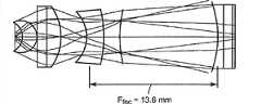
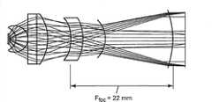
其中,n~1.5用于凝胶密封剂或1.0用于空气。注意,由于LED发光体42的伸展性质,透镜82发射的“经过准直的”光线将实际具有非零角散步。利用常规的光学设计软件,可以对两种设计,即‘801专利申请的化合物封壳透镜与本文所公开的中空腔体设计,进行精确的计算ftot以获得在两种情况下透镜之间的功率分配的更好了解。参考图6所示的表。准直光束子系统在空气中的焦距ftot(2.92mm)比相同球半径,即凹凸透镜相同的外半径的胶囊包封的焦距(2.36mm)长。Among them, n ~ 1.5 for gel sealant or 1.0 for air. Note that due to the stretched nature of
图7A和图7B中示出的总的照明系统具有上述准直光束子系统以及将光引到成像器第二透镜组。由于照明系统为无定焦点(以允许偏振循环利用和/或变形附件),因此可选择第二组透镜的焦距ffoc以保持未改变系统(空气中mag=-4.7)的整体放大。参见图7A-B,其中图7A示出‘801专利申请中照明系统化合物封壳透镜的光学布局,而图7B示出使用中空腔体凹凸透镜(即此处其他系统的内侧透镜更换为空气)的类似照明系统的光学布局。The overall illumination system shown in Figures 7A and 7B has the collimated beam subsystem described above and a second lens group directing the light to the imager. Since the illumination system is focus-agnostic (to allow polarization recycling and/or anamorphic attachments), the focal length ffoc of the second set of lenses can be chosen to keep the overall magnification of the unchanged system (mag = -4.7 in air). See Figures 7A-B, where Figure 7A shows the optical layout of the illumination system compound envelope lens in the '801 patent application, while Figure 7B shows the use of a hollow cavity meniscus lens (i.e., where the inner lens of the other system is replaced with air) The optical layout of the similar lighting system.
注意一个可以略微降低凹凸透镜的厚度以保留空气中的消球差条件。也要注意,总体长度、体积和耦合效率性能类似于这两种设计。Note that one can slightly reduce the meniscus thickness to preserve the aplanatic condition in air. Note also that the overall length, volume, and coupling efficiency performance is similar for both designs.
本发明所公开的紧凑光源也可用于投影系统,例如采用了硅基液晶(LCOS)面板或其它像素化面板的投影系统。同此提交于同一天的共同转让的名称为“Optical Projection Subsystem”(光学投影子系统)(代理人案卷号63281US002)的美国专利申请中公开有示例性投影系统。The disclosed compact light sources can also be used in projection systems, such as those employing liquid crystal on silicon (LCOS) panels or other pixelated panels. An exemplary projection system is disclosed in commonly assigned US Patent Application entitled "Optical Projection Subsystem" (Attorney Docket No. 63281US002), filed on the same date herewith.
例如,图8示出投影子系统200。投影子系统200用于从微型电子系统诸如手机、个人数字助理(PDA)、全球定位系统(GPS)接收器等投影静止或视频图像。投影子系统200从其所嵌入的微型电子系统(图8中未示出)接纳电能和图像数据。投影子系统200用于作为显示计算机视频所必须的微型投影仪的组成部分。投影子系统200用于小到可以携带的系统,当不用时可装入衣服口袋,诸如衬衫口袋。可将由投影子系统200投影的图像投影到反光投影屏幕、经过油漆的浅色墙壁、白板或纸张或其他已知投影表面。投影子系统200可以被嵌入到便携式计算机或手机中。For example, FIG. 8 shows
投影子系统200具有准直光束子系统202,该准直光束子系统可以是本发明所公开的实施例80、90等的准直光束子系统。准直光束子系统202会形成光束204。光引擎包括集合透镜206(如以凹凸透镜46的形式)、准直仪208和固态发光器210。根据一个方面,集合透镜206具有超半球球形透镜。The
固态发光器210接收具有电平的电能212。固态发光体210热耦合至散热器214。固态发光器提供具有发光体光通量水平的发光体光束。根据一个方面,光束204包括非相干光。根据另一个方面,光束204包括固态发光器210的部分聚焦图像的照明。仍然根据另一个方面,固态发光器210具有一个或多个发光二极管(LED)。根据另一个方面,集合透镜206具有半球形透镜。根据另一个方面,准直仪208包括具有第一菲涅耳透镜的聚焦单元,第一菲涅耳透镜具有用于接纳第一非准直光束的第一非小平面化侧以及用于发射准直光束的第一非小平面化侧;而第二菲涅耳透镜具有用于基本上直接接纳准直光束的第二非小平面化侧和用于发射输出光束的第二小平面化侧。根据另一个方面,可以如同此提交于同一天的名称为“LED Mosaic”的美国专利申请(代理人案卷号62370US006)中所示来布置固态发光器210。根据另一个方面,可以如同此提交于同一天的名称为“Integrating Light SourceModule”(集成光源模块)的美国专利申请(代理人案卷号62382US008)中所示来布置准直光束子系统202。Solid
投影子系统200具有折射主体220。折射主体220接收光束204。折射主体220提供偏振光束222。折射主体220包括内部偏振滤波器224。一个偏振分量的光束204被内部偏振滤波器224反射以形成偏振光束222。根据一个方面,根据美国专利公布US 2007/0023941A1(Duncan等人)、美国专利公布US 2007/0024981A1(Duncan等人)、美国专利公布US 2007/0085973A1(Duncan等人)和美国专利公布US2007/0030456(Duncan等人)的一个或多个方面形成或利用折射主体。The
折射主体220具有第一外部透镜表面226和第二外部透镜表面228。根据一个方面,外部透镜表面226、外部透镜表面228具有弯曲透镜表面并具有非零屈光度。根据另一个方面,外部透镜表面226、外部透镜表面228是平的。根据另一个方面,折射主体220在内部偏振滤波器224的相对侧上具有塑性树脂材料主体230、232。根据另一个方面,内部偏振滤波器224具有多层光学薄膜。根据另一个方面,折射主体220具有用作偏振光分束器以及透镜的多功能光学元件。通过将偏振光分束器和透镜功能在多功能折射主体内结合起来,可避免不然在单个分束器和透镜之间的空气界面出现的损耗。The
投影子系统200包括图像形成装置236。图像形成装置236接纳电气输入总线238上的图像数据。图像形成装置236接纳偏振光束222。图像形成装置236根据图像数据选择性地反射偏振光束222。图像形成装置236提供具有相对于偏振光束222的偏振旋转的偏振的图像240。图像形成装置236给折射主体220提供图像240。图像240通过内部偏振滤波器224。根据一个方面,图像形成装置236具有硅上液晶(LCOS)装置。
投影子系统200具有投影透镜组件250。投影透镜组件250具有在252、254、256、258、260处示意性地示出的多个透镜。投影透镜组件250接纳来自折射主体220的图像240。投影透镜组件250提供具有适用于查看的投影光通量水平的图像投影光束262。
除非另外指明,在说明书和权利要求中使用的表示部件的尺寸、数量和物理特性的所有数字应当被理解为由词语“约”来修饰。因此,除非有相反的指示,在上述说明书和所附权利要求中所提出的数值参数为近似值,可根据本领域内的技术人员利用本文所公开的教导内容寻求获得的所需特性而变化。Unless otherwise indicated, all numbers expressing dimensions, quantities and physical characteristics of components used in the specification and claims should be understood as being modified by the word "about". Accordingly, unless indicated to the contrary, the numerical parameters set forth in the foregoing specification and attached claims are approximations that can vary depending upon the desired properties sought to be obtained by those skilled in the art utilizing the teachings disclosed herein.
在不偏离本发明范围和精神的前提下,本发明的各种修改形式和替代形式对于本领域的技术人员来说应是显而易见的,应该理解的是,本发明不限于本文所提供的示例性实施例。Various modifications and alternative forms of the present invention will be apparent to those skilled in the art without departing from the scope and spirit of the present invention. It should be understood that the present invention is not limited to the exemplary embodiments provided herein. Example.
Claims (9)
Translated fromChineseApplications Claiming Priority (3)
| Application Number | Priority Date | Filing Date | Title |
|---|---|---|---|
| US82088706P | 2006-07-31 | 2006-07-31 | |
| US60/820,887 | 2006-07-31 | ||
| PCT/US2007/074830WO2008016908A2 (en) | 2006-07-31 | 2007-07-31 | Led source with hollow collection lens |
Publications (2)
| Publication Number | Publication Date |
|---|---|
| CN101496186A CN101496186A (en) | 2009-07-29 |
| CN101496186Btrue CN101496186B (en) | 2012-11-21 |
Family
ID=38982617
Family Applications (1)
| Application Number | Title | Priority Date | Filing Date |
|---|---|---|---|
| CN2007800284995AExpired - Fee RelatedCN101496186B (en) | 2006-07-31 | 2007-07-31 | LED light source with hollow collecting lens |
Country Status (7)
| Country | Link |
|---|---|
| US (2) | US8115384B2 (en) |
| EP (2) | EP2050147A2 (en) |
| JP (1) | JP2009545894A (en) |
| KR (1) | KR101445404B1 (en) |
| CN (1) | CN101496186B (en) |
| TW (1) | TWI465147B (en) |
| WO (1) | WO2008016908A2 (en) |
Families Citing this family (38)
| Publication number | Priority date | Publication date | Assignee | Title |
|---|---|---|---|---|
| US8662702B2 (en)* | 2009-09-08 | 2014-03-04 | Star Headlight & Lantern Co., Inc. | LED beacon |
| US20040207774A1 (en)* | 2003-04-17 | 2004-10-21 | Gothard David L. | Illumination apparatus for LCD/organic displays |
| EP2049947A1 (en) | 2006-07-31 | 2009-04-22 | 3M Innovative Properties Company | Optical projection subsystem |
| JP2009545894A (en) | 2006-07-31 | 2009-12-24 | スリーエム イノベイティブ プロパティズ カンパニー | LED source with hollow condenser lens |
| KR101328960B1 (en)* | 2007-11-05 | 2013-11-14 | 엘지전자 주식회사 | Projector |
| CN101626054B (en)* | 2008-07-10 | 2011-05-18 | 一品光学工业股份有限公司 | Aspherical wide-angle optical lens and light-emitting diode assembly formed therefrom |
| US8576406B1 (en) | 2009-02-25 | 2013-11-05 | Physical Optics Corporation | Luminaire illumination system and method |
| WO2010103968A1 (en)* | 2009-03-12 | 2010-09-16 | コニカミノルタオプト株式会社 | Optical element, method for manufacturing optical element, light emitting unit, and method for assembling light emitting unit |
| JP5302738B2 (en)* | 2009-04-06 | 2013-10-02 | シャープ株式会社 | Light emitting device and backlight device |
| WO2011046887A1 (en) | 2009-10-14 | 2011-04-21 | 3M Innovative Properties Company | Light source |
| TWI417483B (en)* | 2009-12-25 | 2013-12-01 | Chi Lin Technology Co Ltd | Light source device and backlight module including the light source device |
| JP5493147B2 (en)* | 2010-04-07 | 2014-05-14 | 株式会社エンプラス | Luminous flux control member, light emitting device, and illumination device |
| DE102010014289B4 (en)* | 2010-04-08 | 2014-03-27 | Trilux Gmbh & Co. Kg | Light module and luminaire with light module |
| US8342690B2 (en)* | 2010-04-29 | 2013-01-01 | Eastman Kodak Company | Off-state light baffle for digital projection |
| US9709242B2 (en) | 2010-09-23 | 2017-07-18 | Light Prescriptions Innovators, Llc | Shell integrator |
| WO2012040414A2 (en)* | 2010-09-23 | 2012-03-29 | Light Prescriptions Innovators, Llc | Shell integrator |
| WO2012066654A1 (en)* | 2010-11-17 | 2012-05-24 | Necディスプレイソリューションズ株式会社 | Light source apparatus, lighting apparatus, and projection-type display apparatus |
| TWI418918B (en)* | 2010-11-19 | 2013-12-11 | Wintek Corp | Illumination module and projection apparatus |
| US8556469B2 (en)* | 2010-12-06 | 2013-10-15 | Cree, Inc. | High efficiency total internal reflection optic for solid state lighting luminaires |
| CN102537759B (en)* | 2010-12-10 | 2014-10-08 | 联胜(中国)科技有限公司 | Lighting module and projector |
| DE102010054449B4 (en)* | 2010-12-14 | 2018-10-11 | Trw Automotive Electronics & Components Gmbh | Optical projection device |
| CN102606900B (en)* | 2011-01-25 | 2014-07-23 | 海洋王照明科技股份有限公司 | Color-temperature-adjustable white light emitting diode (LED) light source |
| US20130026902A1 (en)* | 2011-07-28 | 2013-01-31 | Chao-Chuan Chen | Led package for increasing illumination and spotlighting |
| RU2513645C2 (en)* | 2012-06-15 | 2014-04-20 | Инесса Петровна Полякова | Light-emitting diode device |
| RU2513640C2 (en)* | 2012-06-27 | 2014-04-20 | Инесса Петровна Полякова | Light-emitting diode device |
| JP5901036B2 (en) | 2012-07-27 | 2016-04-06 | シャープ株式会社 | Lighting device |
| US20140211173A1 (en)* | 2013-01-30 | 2014-07-31 | 3M Innovative Properties Company | Optical projection subsystem |
| CA2875019C (en) | 2013-12-17 | 2021-04-06 | Ephesus Lighting, Inc. | High intensity led illumination device |
| US10741735B2 (en) | 2014-06-02 | 2020-08-11 | 3M Innovative Properties Company | LED with remote phosphor and shell reflector |
| EP3213354B1 (en)* | 2014-10-27 | 2020-06-17 | Lumileds Holding B.V. | Directional light emitting arrangement and a method of producing the same |
| USD766063S1 (en)* | 2015-02-06 | 2016-09-13 | Terrel Yuki | Cabinet knob |
| US10411173B2 (en)* | 2015-03-31 | 2019-09-10 | Nichia Corporation | Light emitting device and light emitting module using the same |
| USD800376S1 (en) | 2015-12-28 | 2017-10-17 | Ephesus Lighting, Inc. | Light emitting diode (LED) module for a lighting device |
| US9759418B2 (en) | 2015-12-28 | 2017-09-12 | Ephesus Lighting, Inc. | Optical lens structures for light emitting diode (LED) array |
| KR101844795B1 (en) | 2017-05-19 | 2018-04-03 | 배상원 | A learning device capable of experiencing the principle of polarization |
| US11333320B2 (en) | 2018-10-22 | 2022-05-17 | American Sterilizer Company | Retroreflector LED spectrum enhancement method and apparatus |
| KR102787183B1 (en)* | 2019-10-02 | 2025-03-28 | 삼성디스플레이 주식회사 | Display device and fabricating method for display device |
| KR102271494B1 (en)* | 2021-02-09 | 2021-06-30 | 대구보건대학교산학협력단 | Graver for dental technician |
Citations (1)
| Publication number | Priority date | Publication date | Assignee | Title |
|---|---|---|---|---|
| US5349509A (en)* | 1992-02-28 | 1994-09-20 | Ebt Licht-Technik Gmbh | Indicator element |
Family Cites Families (153)
| Publication number | Priority date | Publication date | Assignee | Title |
|---|---|---|---|---|
| US5084807A (en) | 1986-08-22 | 1992-01-28 | U.S. Philips Corporation | Illumination system for LCD projection television |
| US5108172A (en) | 1989-08-11 | 1992-04-28 | Raf Electronics Corp. | Active matrix reflective image plane module and projection system |
| US5022750A (en) | 1989-08-11 | 1991-06-11 | Raf Electronics Corp. | Active matrix reflective projection system |
| US6188460B1 (en) | 1990-06-11 | 2001-02-13 | Reveo, Inc. | Image display panel having a backlighting structure and a single-layer pixelated aray of reflective-type spectral filtering elements where between light is recycled for producing color images with enhanced brightness |
| DE4206215A1 (en)* | 1992-02-28 | 1993-09-16 | Ebt Licht Technik Gmbh | ARRANGEMENT FOR PHASE CONTROL |
| US5335158A (en) | 1992-05-21 | 1994-08-02 | Eastman Kodak Company | High efficiency linear light source |
| US6832724B2 (en) | 1993-03-26 | 2004-12-21 | Symbol Technologies, Inc. | Electro-optical assembly for image projection, especially in portable instruments |
| JPH06309842A (en)* | 1993-04-26 | 1994-11-04 | Sony Corp | Editing equipment |
| US5772265A (en) | 1993-10-20 | 1998-06-30 | Gilbert; Anthony Odell | Door security lock |
| US5882774A (en) | 1993-12-21 | 1999-03-16 | Minnesota Mining And Manufacturing Company | Optical film |
| US5625738A (en) | 1994-06-28 | 1997-04-29 | Corning Incorporated | Apparatus for uniformly illuminating a light valve |
| JPH0876082A (en) | 1994-06-28 | 1996-03-22 | Sharp Corp | Projection display device |
| TW324818B (en) | 1995-09-18 | 1998-01-11 | Motorola Inc | Multi-mode image manifestation apparatus |
| US5592578A (en) | 1995-11-01 | 1997-01-07 | Hewlett-Packard Company | Peripheral optical element for redirecting light from an LED |
| EP0817157A3 (en) | 1996-06-28 | 1998-08-12 | Texas Instruments Incorporated | Improvements in or relating to image display system |
| US5975703A (en) | 1996-09-30 | 1999-11-02 | Digital Optics International | Image projection system |
| US6486997B1 (en) | 1997-10-28 | 2002-11-26 | 3M Innovative Properties Company | Reflective LCD projection system using wide-angle Cartesian polarizing beam splitter |
| US5909322A (en)* | 1997-11-05 | 1999-06-01 | Eastman Kodak Company | Magnifier lens |
| US5886825A (en)* | 1997-11-05 | 1999-03-23 | Eastman Kodak Company | Magnifier Lens |
| JP3614001B2 (en) | 1997-12-03 | 2005-01-26 | セイコーエプソン株式会社 | Projection device |
| US6050690A (en) | 1998-01-08 | 2000-04-18 | Siemens Information And Communication Networks, Inc. | Apparatus and method for focusing a projected image |
| US6091085A (en) | 1998-02-19 | 2000-07-18 | Agilent Technologies, Inc. | GaN LEDs with improved output coupling efficiency |
| JPH11282083A (en) | 1998-03-27 | 1999-10-15 | Minolta Co Ltd | Projector device |
| JP3585097B2 (en) | 1998-06-04 | 2004-11-04 | セイコーエプソン株式会社 | Light source device, optical device and liquid crystal display device |
| TW406442B (en) | 1998-07-09 | 2000-09-21 | Sumitomo Electric Industries | White colored LED and intermediate colored LED |
| US6204523B1 (en) | 1998-11-06 | 2001-03-20 | Lumileds Lighting, U.S., Llc | High stability optical encapsulation and packaging for light-emitting diodes in the green, blue, and near UV range |
| US6573978B1 (en) | 1999-01-26 | 2003-06-03 | Mcguire, Jr. James P. | EUV condenser with non-imaging optics |
| US6200002B1 (en) | 1999-03-26 | 2001-03-13 | Philips Electronics North America Corp. | Luminaire having a reflector for mixing light from a multi-color array of leds |
| DE19918370B4 (en)* | 1999-04-22 | 2006-06-08 | Osram Opto Semiconductors Gmbh | LED white light source with lens |
| WO2001008228A1 (en) | 1999-07-26 | 2001-02-01 | Labosphere Institute | Bulk lens, light emitting body, lighting device and optical information system |
| US6384406B1 (en) | 1999-08-05 | 2002-05-07 | Microvision, Inc. | Active tuning of a torsional resonant structure |
| US6488976B1 (en)* | 1999-12-13 | 2002-12-03 | Affinitea Brewing Technologies, Inc. | Method and apparatus for brewing tea with an espresso machine |
| US6486499B1 (en) | 1999-12-22 | 2002-11-26 | Lumileds Lighting U.S., Llc | III-nitride light-emitting device with increased light generating capability |
| JP3823659B2 (en) | 2000-02-04 | 2006-09-20 | セイコーエプソン株式会社 | projector |
| US6224216B1 (en) | 2000-02-18 | 2001-05-01 | Infocus Corporation | System and method employing LED light sources for a projection display |
| US6456021B1 (en)* | 2000-06-30 | 2002-09-24 | General Electric Company | Rotating variable frequency transformer with high voltage cables |
| US6527411B1 (en) | 2000-08-01 | 2003-03-04 | Visteon Corporation | Collimating lamp |
| JP3497805B2 (en) | 2000-08-29 | 2004-02-16 | オリンパス株式会社 | Image projection display device |
| TW446848B (en) | 2000-11-29 | 2001-07-21 | Acer Comm & Amp Multimedia Inc | Projection system for automatically adjusting focal length and method thereof |
| US6772265B2 (en) | 2000-12-11 | 2004-08-03 | International Business Machines Corporation | Docking station for a laptop computer |
| US6547416B2 (en) | 2000-12-21 | 2003-04-15 | Koninklijke Philips Electronics N.V. | Faceted multi-chip package to provide a beam of uniform white light from multiple monochrome LEDs |
| US6639706B2 (en) | 2001-01-24 | 2003-10-28 | Kollsman, Inc. | Optical path switch and method of using thereof |
| JP2002222989A (en) | 2001-01-26 | 2002-08-09 | Toshiba Corp | Semiconductor light emitting device |
| AU4374601A (en) | 2001-05-08 | 2002-11-14 | Digislide International Pty Ltd | A portable image projection device |
| US20020176015A1 (en) | 2001-05-23 | 2002-11-28 | Lichtfuss Hans A. | Image capturing camera and projector device |
| US6939499B2 (en) | 2001-05-31 | 2005-09-06 | 3M Innovative Properties Company | Processes and apparatus for making transversely drawn films with substantially uniaxial character |
| US6672721B2 (en) | 2001-06-11 | 2004-01-06 | 3M Innovative Properties Company | Projection system having low astigmatism |
| US6609795B2 (en) | 2001-06-11 | 2003-08-26 | 3M Innovative Properties Company | Polarizing beam splitter |
| US6793344B2 (en) | 2001-06-26 | 2004-09-21 | Integrated Microdisplays Limited | Optical systems for liquid crystal display projectors |
| US6856466B2 (en) | 2001-07-05 | 2005-02-15 | Science & Engineering Associates, Inc. | Multiple imaging system |
| JP4620909B2 (en) | 2001-07-26 | 2011-01-26 | 日東光学株式会社 | Image input / output device |
| US6791749B2 (en) | 2001-08-29 | 2004-09-14 | Delpico Joseph | Polarized exposure for web manufacture |
| JP3948650B2 (en) | 2001-10-09 | 2007-07-25 | アバゴ・テクノロジーズ・イーシービーユー・アイピー(シンガポール)プライベート・リミテッド | Light emitting diode and manufacturing method thereof |
| AU2002359708A1 (en) | 2001-12-14 | 2003-07-15 | Digital Optics International Corporation | Uniform illumination system |
| TW571119B (en) | 2001-12-20 | 2004-01-11 | Delta Electronics Inc | Image projection device with integrated semiconductor light emitting element light source |
| EP1478965A1 (en) | 2002-02-28 | 2004-11-24 | 3M Innovative Properties Company | Compound polarization beam splitters |
| JP3991764B2 (en) | 2002-05-10 | 2007-10-17 | セイコーエプソン株式会社 | Illumination device and projection display device |
| CA2427559A1 (en) | 2002-05-15 | 2003-11-15 | Sumitomo Electric Industries, Ltd. | White color light emitting device |
| US7336403B2 (en)* | 2002-05-27 | 2008-02-26 | Canon Kabushiki Kaisha | Optical element and illumination apparatus having same |
| EP1387211B1 (en) | 2002-07-15 | 2005-05-25 | Sony International (Europe) GmbH | Image recording device combined with image projection capabilities |
| US7306603B2 (en) | 2002-08-21 | 2007-12-11 | Innovative Spinal Technologies | Device and method for percutaneous placement of lumbar pedicle screws and connecting rods |
| CN100468791C (en)* | 2002-08-30 | 2009-03-11 | 吉尔科有限公司 | Light emitting diode with improved effience |
| JP4078159B2 (en) | 2002-09-11 | 2008-04-23 | キヤノン株式会社 | Projection display device and image display system |
| US6936209B2 (en) | 2002-11-27 | 2005-08-30 | 3M Innovative Properties Company | Methods and devices for processing polymer films |
| US6949212B2 (en) | 2002-11-27 | 2005-09-27 | 3M Innovative Properties Company | Methods and devices for stretching polymer films |
| JP4397394B2 (en) | 2003-01-24 | 2010-01-13 | ディジタル・オプティクス・インターナショナル・コーポレイション | High density lighting system |
| US7091661B2 (en) | 2003-01-27 | 2006-08-15 | 3M Innovative Properties Company | Phosphor based light sources having a reflective polarizer |
| KR20050113200A (en)* | 2003-02-26 | 2005-12-01 | 크리, 인코포레이티드 | Composite white light source and method for fabricating |
| US20060279662A1 (en) | 2003-03-16 | 2006-12-14 | Explay Ltd. | Projection system and method |
| US20040218387A1 (en) | 2003-03-18 | 2004-11-04 | Robert Gerlach | LED lighting arrays, fixtures and systems and method for determining human color perception |
| JP4082332B2 (en) | 2003-04-11 | 2008-04-30 | セイコーエプソン株式会社 | Display device and projector |
| FI20030583A7 (en) | 2003-04-16 | 2004-10-17 | Upstream Eng Oy | Data projector |
| US7152977B2 (en) | 2003-04-24 | 2006-12-26 | Qubic Light Corporation | Solid state light engine optical system |
| DE10319274A1 (en) | 2003-04-29 | 2004-12-02 | Osram Opto Semiconductors Gmbh | light source |
| US7237899B2 (en) | 2003-05-16 | 2007-07-03 | 3M Innovative Properties Company | Highly efficient single panel and two panel projection engines |
| US6869206B2 (en) | 2003-05-23 | 2005-03-22 | Scott Moore Zimmerman | Illumination systems utilizing highly reflective light emitting diodes and light recycling to enhance brightness |
| JP2004354881A (en)* | 2003-05-30 | 2004-12-16 | Seiko Epson Corp | Lighting device and projection display device |
| US6903382B2 (en)* | 2003-07-07 | 2005-06-07 | Lightop Technology Co., Ltd. | Light emitting diode mounting structure |
| DE102004034166B4 (en)* | 2003-07-17 | 2015-08-20 | Toyoda Gosei Co., Ltd. | Light-emitting device |
| US6981642B2 (en) | 2003-07-17 | 2006-01-03 | Symbol Technologies, Inc. | Non-parallax optical auto-focusing system and method |
| US7009213B2 (en) | 2003-07-31 | 2006-03-07 | Lumileds Lighting U.S., Llc | Light emitting devices with improved light extraction efficiency |
| US6981542B2 (en)* | 2003-10-29 | 2006-01-03 | Rotys Inc. | Multi-heatsink integrated cooler |
| TWI303110B (en)* | 2003-11-25 | 2008-11-11 | Matsushita Electric Works Ltd | Light-emitting device using light-emitting diode chip |
| US7403680B2 (en) | 2003-12-02 | 2008-07-22 | 3M Innovative Properties Company | Reflective light coupler |
| US7473013B2 (en)* | 2003-12-10 | 2009-01-06 | Okaya Electric Industries Co., Ltd. | Indicator lamp having a converging lens |
| US20050135113A1 (en) | 2003-12-18 | 2005-06-23 | Harvatek Corporation | Optical projection device of a colored lighting module |
| KR100549268B1 (en)* | 2003-12-31 | 2006-02-03 | 동부아남반도체 주식회사 | Phase inversion mask and manufacturing method thereof |
| US7164811B2 (en) | 2004-02-09 | 2007-01-16 | Northrop Grumman Corporation | Pocket-pen ultra-high resolution MEMS projection display in combination with on-axis CCD image capture system including means for permitting 3-D imaging |
| US7246923B2 (en) | 2004-02-11 | 2007-07-24 | 3M Innovative Properties Company | Reshaping light source modules and illumination systems using the same |
| US7300177B2 (en) | 2004-02-11 | 2007-11-27 | 3M Innovative Properties | Illumination system having a plurality of light source modules disposed in an array with a non-radially symmetrical aperture |
| US20050179041A1 (en) | 2004-02-18 | 2005-08-18 | Lumileds Lighting U.S., Llc | Illumination system with LEDs |
| TWI241042B (en)* | 2004-03-11 | 2005-10-01 | Chen-Lun Hsingchen | A low thermal resistance LED device |
| US7215882B2 (en) | 2004-07-21 | 2007-05-08 | Angatrom, Inc. | High-speed automatic focusing system |
| JP2005283663A (en) | 2004-03-26 | 2005-10-13 | Canon Inc | Display optical system and image projection apparatus |
| US7133211B2 (en) | 2004-04-02 | 2006-11-07 | Integrated Microdisplays Limited | Projector with flat light sources |
| GB2413858A (en) | 2004-05-06 | 2005-11-09 | * Agilent Technologies, Inc. | Optical beam-splitter with plano convex lens |
| US7101050B2 (en) | 2004-05-14 | 2006-09-05 | 3M Innovative Properties Company | Illumination system with non-radially symmetrical aperture |
| US7280288B2 (en)* | 2004-06-04 | 2007-10-09 | Cree, Inc. | Composite optical lens with an integrated reflector |
| US7456499B2 (en)* | 2004-06-04 | 2008-11-25 | Cree, Inc. | Power light emitting die package with reflecting lens and the method of making the same |
| DE102004031732A1 (en) | 2004-06-30 | 2006-01-19 | Osram Opto Semiconductors Gmbh | Radiation-emitting semiconductor chip with a beam-shaping element and beam-shaping element |
| US7692861B2 (en) | 2004-07-06 | 2010-04-06 | Real D | Illumination systems |
| KR100638611B1 (en)* | 2004-08-12 | 2006-10-26 | 삼성전기주식회사 | Multi Lens Light Emitting Diode |
| US7390097B2 (en) | 2004-08-23 | 2008-06-24 | 3M Innovative Properties Company | Multiple channel illumination system |
| JP4559162B2 (en) | 2004-08-30 | 2010-10-06 | ソフトバンクモバイル株式会社 | Information communication terminal |
| US20060055838A1 (en) | 2004-09-13 | 2006-03-16 | Eastman Kodak Company | Light recycling film and display |
| US7352124B2 (en)* | 2004-09-28 | 2008-04-01 | Goldeneye, Inc. | Light recycling illumination systems utilizing light emitting diodes |
| KR101080355B1 (en) | 2004-10-18 | 2011-11-04 | 삼성전자주식회사 | Light emitting diode, lens for the same |
| US7255448B2 (en) | 2004-10-20 | 2007-08-14 | Hewlett-Packard Development Company, L.P. | Pixelated color management display |
| US20060091411A1 (en) | 2004-10-29 | 2006-05-04 | Ouderkirk Andrew J | High brightness LED package |
| US7329982B2 (en) | 2004-10-29 | 2008-02-12 | 3M Innovative Properties Company | LED package with non-bonded optical element |
| US7330319B2 (en) | 2004-10-29 | 2008-02-12 | 3M Innovative Properties Company | High brightness LED package with multiple optical elements |
| US7304425B2 (en) | 2004-10-29 | 2007-12-04 | 3M Innovative Properties Company | High brightness LED package with compound optical element(s) |
| US7352011B2 (en) | 2004-11-15 | 2008-04-01 | Philips Lumileds Lighting Company, Llc | Wide emitting lens for LED useful for backlighting |
| US7745814B2 (en) | 2004-12-09 | 2010-06-29 | 3M Innovative Properties Company | Polychromatic LED's and related semiconductor devices |
| US7168820B1 (en) | 2004-12-21 | 2007-01-30 | Djirair Minassian | Lighted vase |
| US20060232578A1 (en) | 2004-12-21 | 2006-10-19 | Silviu Reinhorn | Collapsible portable display |
| US20060139575A1 (en) | 2004-12-23 | 2006-06-29 | Upstream Engineering Oy | Optical collection and distribution system and method |
| US7543941B2 (en) | 2004-12-23 | 2009-06-09 | Cooper Technologies Company | Light zoom source using light emitting diodes and an improved method of collecting the energy radiating from them |
| KR101114305B1 (en)* | 2004-12-24 | 2012-03-08 | 쿄세라 코포레이션 | Light-emitting device and illuminating device |
| GB0428381D0 (en) | 2004-12-24 | 2005-02-02 | Isis Innovation | Vaccine |
| US20060139580A1 (en) | 2004-12-29 | 2006-06-29 | Conner Arlie R | Illumination system using multiple light sources with integrating tunnel and projection systems using same |
| US7692207B2 (en) | 2005-01-21 | 2010-04-06 | Luminus Devices, Inc. | Packaging designs for LEDs |
| JP4468843B2 (en)* | 2005-03-09 | 2010-05-26 | 日東電工株式会社 | Manufacturing method of optical waveguide |
| US7422330B2 (en) | 2005-03-30 | 2008-09-09 | 3M Innovative Properties Company | Illumination system and projection system using same |
| US7445340B2 (en) | 2005-05-19 | 2008-11-04 | 3M Innovative Properties Company | Polarized, LED-based illumination source |
| US7410261B2 (en) | 2005-05-20 | 2008-08-12 | 3M Innovative Properties Company | Multicolor illuminator system |
| US7529029B2 (en) | 2005-07-29 | 2009-05-05 | 3M Innovative Properties Company | Polarizing beam splitter |
| US20070023941A1 (en) | 2005-07-29 | 2007-02-01 | Duncan John E | Method for making polarizing beam splitters |
| US7362507B2 (en) | 2005-07-29 | 2008-04-22 | 3M Innovative Properties Company | Polarizing beam splitter |
| JP4180591B2 (en)* | 2005-08-04 | 2008-11-12 | 株式会社椿本チエイン | Plastic hydraulic tensioner |
| CN100438026C (en) | 2005-09-16 | 2008-11-26 | 鸿富锦精密工业(深圳)有限公司 | White light light-emitting diode and producing method thereof |
| FR2891607B1 (en)* | 2005-10-05 | 2007-12-28 | Degre K Sa | DIODE LIGHTING DEVICE. |
| US7540616B2 (en) | 2005-12-23 | 2009-06-02 | 3M Innovative Properties Company | Polarized, multicolor LED-based illumination source |
| US7369320B2 (en) | 2005-12-30 | 2008-05-06 | 3M Innovative Properties Company | Projection system with beam homogenizer |
| US7798678B2 (en) | 2005-12-30 | 2010-09-21 | 3M Innovative Properties Company | LED with compound encapsulant lens |
| US20070153402A1 (en) | 2005-12-30 | 2007-07-05 | Destain Patrick R | Fresnel lens combination |
| US20070191506A1 (en) | 2006-02-13 | 2007-08-16 | 3M Innovative Properties Company | Curable compositions for optical articles |
| US7463417B2 (en) | 2006-02-13 | 2008-12-09 | 3M Innovative Properties Company | Optical articles from curable compositions |
| US7423297B2 (en) | 2006-05-03 | 2008-09-09 | 3M Innovative Properties Company | LED extractor composed of high index glass |
| US20090128781A1 (en) | 2006-06-13 | 2009-05-21 | Kenneth Li | LED multiplexer and recycler and micro-projector incorporating the Same |
| US20070297052A1 (en) | 2006-06-26 | 2007-12-27 | Bin Wang | Cube wire-grid polarizing beam splitter |
| US20070296921A1 (en) | 2006-06-26 | 2007-12-27 | Bin Wang | Projection display with a cube wire-grid polarizing beam splitter |
| US20080013051A1 (en) | 2006-07-14 | 2008-01-17 | 3M Innovative Properties Company | Polarizing beam splitters incorporating reflective and absorptive polarizers and image display systems thereof |
| CN101496170B (en) | 2006-07-31 | 2011-06-29 | 3M创新有限公司 | Integrated light source module |
| US20080036972A1 (en) | 2006-07-31 | 2008-02-14 | 3M Innovative Properties Company | Led mosaic |
| JP2009545894A (en) | 2006-07-31 | 2009-12-24 | スリーエム イノベイティブ プロパティズ カンパニー | LED source with hollow condenser lens |
| US20080051135A1 (en) | 2006-07-31 | 2008-02-28 | 3M Innovative Properties Company | Combination camera/projector system |
| EP2049947A1 (en) | 2006-07-31 | 2009-04-22 | 3M Innovative Properties Company | Optical projection subsystem |
| US8075140B2 (en) | 2006-07-31 | 2011-12-13 | 3M Innovative Properties Company | LED illumination system with polarization recycling |
| US20080231780A1 (en) | 2007-03-22 | 2008-09-25 | Sabic Innovative Plastics Ip Bv | Low-absorptive diffuser sheet and film stacks for direct-lit backlighting |
| US20080231953A1 (en) | 2007-03-22 | 2008-09-25 | Young Garrett J | System and Method for LED Polarization Recycling |
| US8540375B2 (en) | 2007-11-30 | 2013-09-24 | Texas Instruments Incorporated | Offset projection distortion correction |
| US20090310042A1 (en) | 2008-06-16 | 2009-12-17 | Marcial Vidal | Illumination system and method with efficient polarization recovery |
- 2007
- 2007-07-31JPJP2009523012Apatent/JP2009545894A/ennot_activeWithdrawn
- 2007-07-31TWTW096128133Apatent/TWI465147B/ennot_activeIP Right Cessation
- 2007-07-31USUS11/831,171patent/US8115384B2/ennot_activeExpired - Fee Related
- 2007-07-31WOPCT/US2007/074830patent/WO2008016908A2/enactiveApplication Filing
- 2007-07-31KRKR1020097001992Apatent/KR101445404B1/ennot_activeExpired - Fee Related
- 2007-07-31EPEP07813580Apatent/EP2050147A2/ennot_activeWithdrawn
- 2007-07-31CNCN2007800284995Apatent/CN101496186B/ennot_activeExpired - Fee Related
- 2007-07-31EPEP11171672.6Apatent/EP2372797A3/ennot_activeWithdrawn
- 2011
- 2011-06-14USUS13/159,895patent/US8274220B2/ennot_activeExpired - Fee Related
Patent Citations (1)
| Publication number | Priority date | Publication date | Assignee | Title |
|---|---|---|---|---|
| US5349509A (en)* | 1992-02-28 | 1994-09-20 | Ebt Licht-Technik Gmbh | Indicator element |
Non-Patent Citations (1)
| Title |
|---|
| Design of collection systems for multi-LED light engines;HUSEYIN M;《PROCEEDINGS OF SPIE》;20060421;第6196卷;第3-6页* |
Also Published As
| Publication number | Publication date |
|---|---|
| TW200814844A (en) | 2008-03-16 |
| EP2372797A2 (en) | 2011-10-05 |
| US20110241518A1 (en) | 2011-10-06 |
| EP2050147A2 (en) | 2009-04-22 |
| US20080048553A1 (en) | 2008-02-28 |
| CN101496186A (en) | 2009-07-29 |
| WO2008016908A2 (en) | 2008-02-07 |
| KR20090037901A (en) | 2009-04-16 |
| US8115384B2 (en) | 2012-02-14 |
| KR101445404B1 (en) | 2014-09-26 |
| EP2372797A3 (en) | 2017-01-18 |
| US8274220B2 (en) | 2012-09-25 |
| WO2008016908A3 (en) | 2008-06-12 |
| JP2009545894A (en) | 2009-12-24 |
| TWI465147B (en) | 2014-12-11 |
Similar Documents
| Publication | Publication Date | Title |
|---|---|---|
| CN101496186B (en) | LED light source with hollow collecting lens | |
| US7798678B2 (en) | LED with compound encapsulant lens | |
| CN101598294B (en) | Collimating lens, lighting unit and projection system | |
| TWI431323B (en) | Collimator lens, illumination unit and projection system | |
| JP4799341B2 (en) | Lighting device | |
| CN101496170B (en) | Integrated light source module | |
| US8003998B2 (en) | Light-emitting diode arrangement | |
| CN100524001C (en) | Light source unit and projector | |
| US20230152590A1 (en) | Compact polarized illuminators using reflective polarizers | |
| CN101459211A (en) | Solid illuminating device | |
| JP2004281605A (en) | LED package | |
| CN106463591A (en) | LED with remote phosphor and shell reflector | |
| US20110057557A1 (en) | Projection led module and method of making a projection led module | |
| CN110531574A (en) | The manufacturing method of light supply apparatus, projector and light supply apparatus | |
| US7976200B2 (en) | Optical projection device | |
| CN119008819A (en) | Light-emitting element and projection device | |
| US20080044142A1 (en) | Light emitting diode module | |
| CN115032779A (en) | Optical module and optical equipment | |
| TW201111835A (en) | Projection LED module and method of making a projection LED module | |
| JP2025079729A (en) | Light emitting module and smartphone | |
| CN119029123A (en) | Inorganic display panel | |
| TW200929596A (en) | Solid state light emitting device | |
| TW201213870A (en) | Lens and LED module | |
| TW200812103A (en) | Light-emitting diode module |
Legal Events
| Date | Code | Title | Description |
|---|---|---|---|
| C06 | Publication | ||
| PB01 | Publication | ||
| C10 | Entry into substantive examination | ||
| SE01 | Entry into force of request for substantive examination | ||
| C14 | Grant of patent or utility model | ||
| GR01 | Patent grant | ||
| CF01 | Termination of patent right due to non-payment of annual fee | ||
| CF01 | Termination of patent right due to non-payment of annual fee | Granted publication date:20121121 Termination date:20180731 |