CN101494205B - Integrated circuit package and manufacturing method thereof - Google Patents
Integrated circuit package and manufacturing method thereofDownload PDFInfo
- Publication number
- CN101494205B CN101494205BCN2008100041699ACN200810004169ACN101494205BCN 101494205 BCN101494205 BCN 101494205BCN 2008100041699 ACN2008100041699 ACN 2008100041699ACN 200810004169 ACN200810004169 ACN 200810004169ACN 101494205 BCN101494205 BCN 101494205B
- Authority
- CN
- China
- Prior art keywords
- heat dissipation
- dissipation layer
- integrated circuit
- substrate
- circuit package
- Prior art date
- Legal status (The legal status is an assumption and is not a legal conclusion. Google has not performed a legal analysis and makes no representation as to the accuracy of the status listed.)
- Active
Links
- 238000004519manufacturing processMethods0.000titleclaimsdescription45
- 230000017525heat dissipationEffects0.000claimsabstractdescription152
- 239000000758substrateSubstances0.000claimsabstractdescription99
- 238000000034methodMethods0.000claimsdescription21
- 238000009713electroplatingMethods0.000claimsdescription19
- 238000005229chemical vapour depositionMethods0.000claimsdescription16
- 238000005240physical vapour depositionMethods0.000claimsdescription16
- 229920005989resinPolymers0.000claimsdescription13
- 239000011347resinSubstances0.000claimsdescription13
- 238000005530etchingMethods0.000claimsdescription12
- 229920002120photoresistant polymerPolymers0.000claimsdescription10
- 229910052751metalInorganic materials0.000claimsdescription9
- 239000002184metalSubstances0.000claimsdescription9
- RYGMFSIKBFXOCR-UHFFFAOYSA-NCopperChemical compound[Cu]RYGMFSIKBFXOCR-UHFFFAOYSA-N0.000claimsdescription6
- BQCADISMDOOEFD-UHFFFAOYSA-NSilverChemical compound[Ag]BQCADISMDOOEFD-UHFFFAOYSA-N0.000claimsdescription6
- 229910052802copperInorganic materials0.000claimsdescription6
- 239000010949copperSubstances0.000claimsdescription6
- PCHJSUWPFVWCPO-UHFFFAOYSA-NgoldChemical compound[Au]PCHJSUWPFVWCPO-UHFFFAOYSA-N0.000claimsdescription6
- 229910052737goldInorganic materials0.000claimsdescription6
- 239000010931goldSubstances0.000claimsdescription6
- 229910052709silverInorganic materials0.000claimsdescription6
- 239000004332silverSubstances0.000claimsdescription6
- 238000005553drillingMethods0.000claimsdescription5
- 239000010410layerSubstances0.000description174
- 239000004020conductorSubstances0.000description49
- 239000004065semiconductorSubstances0.000description35
- 239000000463materialSubstances0.000description12
- 238000001459lithographyMethods0.000description4
- 238000007639printingMethods0.000description4
- 238000007650screen-printingMethods0.000description4
- 238000004904shorteningMethods0.000description4
- 238000005538encapsulationMethods0.000description3
- 238000004806packaging method and processMethods0.000description3
- 235000012431wafersNutrition0.000description3
- 229910000881Cu alloyInorganic materials0.000description2
- 239000004642PolyimideSubstances0.000description2
- 239000012790adhesive layerSubstances0.000description2
- 229910052782aluminiumInorganic materials0.000description2
- XAGFODPZIPBFFR-UHFFFAOYSA-NaluminiumChemical compound[Al]XAGFODPZIPBFFR-UHFFFAOYSA-N0.000description2
- 238000007747platingMethods0.000description2
- 229920001721polyimidePolymers0.000description2
- 229910000679solderInorganic materials0.000description2
- 230000002159abnormal effectEffects0.000description1
- 239000000853adhesiveSubstances0.000description1
- 230000001070adhesive effectEffects0.000description1
- 230000005540biological transmissionEffects0.000description1
- 230000000694effectsEffects0.000description1
- 238000005516engineering processMethods0.000description1
- 239000003822epoxy resinSubstances0.000description1
- 238000009413insulationMethods0.000description1
- 238000012986modificationMethods0.000description1
- 230000004048modificationEffects0.000description1
- 238000000059patterningMethods0.000description1
- 229920000647polyepoxidePolymers0.000description1
- 239000002356single layerSubstances0.000description1
Images


Classifications
- H—ELECTRICITY
- H01—ELECTRIC ELEMENTS
- H01L—SEMICONDUCTOR DEVICES NOT COVERED BY CLASS H10
- H01L2224/00—Indexing scheme for arrangements for connecting or disconnecting semiconductor or solid-state bodies and methods related thereto as covered by H01L24/00
- H01L2224/01—Means for bonding being attached to, or being formed on, the surface to be connected, e.g. chip-to-package, die-attach, "first-level" interconnects; Manufacturing methods related thereto
- H01L2224/42—Wire connectors; Manufacturing methods related thereto
- H01L2224/47—Structure, shape, material or disposition of the wire connectors after the connecting process
- H01L2224/48—Structure, shape, material or disposition of the wire connectors after the connecting process of an individual wire connector
- H01L2224/4805—Shape
- H01L2224/4809—Loop shape
- H01L2224/48091—Arched
- H—ELECTRICITY
- H01—ELECTRIC ELEMENTS
- H01L—SEMICONDUCTOR DEVICES NOT COVERED BY CLASS H10
- H01L2224/00—Indexing scheme for arrangements for connecting or disconnecting semiconductor or solid-state bodies and methods related thereto as covered by H01L24/00
- H01L2224/01—Means for bonding being attached to, or being formed on, the surface to be connected, e.g. chip-to-package, die-attach, "first-level" interconnects; Manufacturing methods related thereto
- H01L2224/42—Wire connectors; Manufacturing methods related thereto
- H01L2224/47—Structure, shape, material or disposition of the wire connectors after the connecting process
- H01L2224/48—Structure, shape, material or disposition of the wire connectors after the connecting process of an individual wire connector
- H01L2224/481—Disposition
- H01L2224/48151—Connecting between a semiconductor or solid-state body and an item not being a semiconductor or solid-state body, e.g. chip-to-substrate, chip-to-passive
- H01L2224/48221—Connecting between a semiconductor or solid-state body and an item not being a semiconductor or solid-state body, e.g. chip-to-substrate, chip-to-passive the body and the item being stacked
- H01L2224/48225—Connecting between a semiconductor or solid-state body and an item not being a semiconductor or solid-state body, e.g. chip-to-substrate, chip-to-passive the body and the item being stacked the item being non-metallic, e.g. insulating substrate with or without metallisation
- H01L2224/4824—Connecting between the body and an opposite side of the item with respect to the body
- H—ELECTRICITY
- H01—ELECTRIC ELEMENTS
- H01L—SEMICONDUCTOR DEVICES NOT COVERED BY CLASS H10
- H01L2924/00—Indexing scheme for arrangements or methods for connecting or disconnecting semiconductor or solid-state bodies as covered by H01L24/00
- H01L2924/01—Chemical elements
- H01L2924/01078—Platinum [Pt]
- H—ELECTRICITY
- H01—ELECTRIC ELEMENTS
- H01L—SEMICONDUCTOR DEVICES NOT COVERED BY CLASS H10
- H01L2924/00—Indexing scheme for arrangements or methods for connecting or disconnecting semiconductor or solid-state bodies as covered by H01L24/00
- H01L2924/01—Chemical elements
- H01L2924/01079—Gold [Au]
- H—ELECTRICITY
- H01—ELECTRIC ELEMENTS
- H01L—SEMICONDUCTOR DEVICES NOT COVERED BY CLASS H10
- H01L2924/00—Indexing scheme for arrangements or methods for connecting or disconnecting semiconductor or solid-state bodies as covered by H01L24/00
- H01L2924/10—Details of semiconductor or other solid state devices to be connected
- H01L2924/11—Device type
- H01L2924/14—Integrated circuits
- H—ELECTRICITY
- H01—ELECTRIC ELEMENTS
- H01L—SEMICONDUCTOR DEVICES NOT COVERED BY CLASS H10
- H01L2924/00—Indexing scheme for arrangements or methods for connecting or disconnecting semiconductor or solid-state bodies as covered by H01L24/00
- H01L2924/15—Details of package parts other than the semiconductor or other solid state devices to be connected
- H01L2924/151—Die mounting substrate
- H01L2924/153—Connection portion
- H01L2924/1531—Connection portion the connection portion being formed only on the surface of the substrate opposite to the die mounting surface
- H01L2924/15311—Connection portion the connection portion being formed only on the surface of the substrate opposite to the die mounting surface being a ball array, e.g. BGA
Landscapes
- Cooling Or The Like Of Semiconductors Or Solid State Devices (AREA)
Abstract
Description
Translated fromChinese技术领域technical field
本发明涉及一种集成电路封装体,特别是有关于一种集成电路封装体的制造方法。The invention relates to an integrated circuit package, in particular to a manufacturing method of the integrated circuit package.
背景技术Background technique
在半导体工业中,集成电路一般形成在晶片上,其中,在同一片晶片上的多个半导体芯片可同时形成,因此,这些半导体芯片随后可从晶片上切割出来,然而由于这些半导体芯片体积既小且易碎,因此在使用这些芯片之前必须先予以封装。In the semiconductor industry, integrated circuits are generally formed on wafers, wherein a plurality of semiconductor chips on the same wafer can be formed at the same time, therefore, these semiconductor chips can be cut out from the wafer later, however, due to the small size of these semiconductor chips And fragile, so these chips must be packaged before using them.
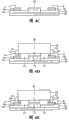
图1显示了传统的集成电路封装体,其包括半导体芯片12。首先,利用黏着层14将半导体芯片12贴附于封装基板10上。随后,将锡球16形成于封装基板10的表面上,且电性连接印刷电路板18。最后再填入封装树脂20,以包覆上述半导体芯片12。由于封装树脂20与封装基板10两者皆不是良好的导热材料,以致于半导体芯片12所产生的热会局限在集成电路封装体内,而导致半导体芯片12的寿命缩短或操作异常。FIG. 1 shows a conventional integrated circuit package including a semiconductor chip 12 . Firstly, the semiconductor chip 12 is attached to the package substrate 10 by the adhesive layer 14 . Subsequently, solder balls 16 are formed on the surface of the packaging substrate 10 and electrically connected to the printed circuit board 18 . Finally, the encapsulation resin 20 is filled to cover the above-mentioned semiconductor chip 12 . Since both the encapsulation resin 20 and the encapsulation substrate 10 are not good heat-conducting materials, the heat generated by the semiconductor chip 12 will be confined in the integrated circuit package, resulting in shortened lifespan or abnormal operation of the semiconductor chip 12 .
因此,因此需要一种新颖的封装结构来改善上述问题。Therefore, a novel packaging structure is needed to improve the above problems.
发明内容Contents of the invention
因此,本发明的一个目的是提供一种集成电路封装体,包括:基板,具有第一表面、及相对的第二表面,以及第一孔洞,其中该第一孔洞从该基板的第一表面贯穿至该第二表面;多个导线,设置于该基板的第二表面的一部分上;芯片,设置于该基板的第二表面的上方,两者之间形成腔室;多个接合垫,设置于该芯片朝向该基板的第二表面的一侧,且这些接合垫的至少一个与这些导线中的一个电性连接;以及第一散热层,从该第一孔洞延伸至该腔室内。Therefore, an object of the present invention is to provide an integrated circuit package, comprising: a substrate having a first surface, an opposite second surface, and a first hole, wherein the first hole penetrates from the first surface of the substrate To the second surface; a plurality of wires, disposed on a part of the second surface of the substrate; chips, disposed above the second surface of the substrate, forming a cavity therebetween; a plurality of bonding pads, disposed on The chip faces the side of the second surface of the substrate, and at least one of the bonding pads is electrically connected to one of the wires; and a first heat dissipation layer extends from the first hole into the chamber.
根据本发明的集成电路封装体,其中第一散热层填满第一孔洞并与芯片连接。According to the integrated circuit package of the present invention, wherein the first heat dissipation layer fills the first hole and is connected to the chip.
根据本发明的集成电路封装体,其中第一散热层从基板的第一表面延伸至第一孔洞中,且穿过第一孔洞并与芯片连接。According to the integrated circuit package of the present invention, wherein the first heat dissipation layer extends from the first surface of the substrate into the first hole, passes through the first hole and is connected to the chip.
根据本发明的集成电路封装体,进一步包括在芯片朝向基板的第二表面的一侧设置第二散热层,且第二散热层连接该第一散热层。According to the integrated circuit package of the present invention, a second heat dissipation layer is provided on the side of the chip facing the second surface of the substrate, and the second heat dissipation layer is connected to the first heat dissipation layer.
根据本发明的集成电路封装体,其中该第一散热层从基板的第一表面穿过第一孔洞且延伸至基板的第二表面上。According to the integrated circuit package of the present invention, wherein the first heat dissipation layer passes through the first hole from the first surface of the substrate and extends to the second surface of the substrate.
根据本发明的集成电路封装体,其中第二表面上的第一散热层与接合垫之一连接。According to the integrated circuit package of the present invention, wherein the first heat dissipation layer on the second surface is connected to one of the bonding pads.
根据本发明的集成电路封装体,其中该第一散热层与芯片及接合垫之间相隔一既定距离。According to the integrated circuit package of the present invention, there is a predetermined distance between the first heat dissipation layer and the chip and the bonding pad.
根据本发明的集成电路封装体,还包括第三散热层,从基板的第一表面穿过第二孔洞且延伸至该基板的第二表面上,其中该第二孔洞与该第一孔洞相邻。The integrated circuit package according to the present invention further includes a third heat dissipation layer extending from the first surface of the substrate through the second hole to the second surface of the substrate, wherein the second hole is adjacent to the first hole .
根据本发明的集成电路封装体,其中该第三散热层与芯片及这些接合垫之间相隔一既定距离。According to the integrated circuit package of the present invention, the third heat dissipation layer is separated from the chip and the bonding pads by a predetermined distance.
根据本发明的集成电路封装体,进一步包括在芯片朝向基板的第二表面的一侧设置第四散热层,且该第四散热层连接该第三散热层。According to the integrated circuit package of the present invention, a fourth heat dissipation layer is disposed on the side of the chip facing the second surface of the substrate, and the fourth heat dissipation layer is connected to the third heat dissipation layer.
根据本发明的集成电路封装体,进一步包括树脂,填入腔室内以密封芯片与基板之间的第一散热层。The integrated circuit package according to the present invention further includes a resin filled into the cavity to seal the first heat dissipation layer between the chip and the substrate.
根据本发明的集成电路封装体,其中第一散热层由金、银或铜金属组成。According to the integrated circuit package of the present invention, wherein the first heat dissipation layer is composed of gold, silver or copper metal.
本发的另一目的是提供一种集成电路封装体的制造方法,包括:提供基板,具有第一表面、及相对的第二表面,以及第一孔洞,其中该第一孔洞从该基板的第一表面贯穿至该第二表面;在该第一表面上形成第一散热层;在该第二表面的一部分上形成多个导线;提供芯片,设置于该基板的第二表面的上方,两者之间形成腔室;形成多个接合垫于该芯片朝向于该基板的第二表面的一侧,其中这些接合垫中的至少一个与这些导线的一个电性连接;以及形成第二散热层,从该第一孔洞延伸至该腔室内,且该第二散热层与该第一散热层接触。Another object of the present invention is to provide a method of manufacturing an integrated circuit package, comprising: providing a substrate having a first surface, an opposite second surface, and a first hole, wherein the first hole extends from the first surface of the substrate A surface penetrates to the second surface; a first heat dissipation layer is formed on the first surface; a plurality of wires are formed on a part of the second surface; a chip is provided above the second surface of the substrate, and both forming a cavity therebetween; forming a plurality of bonding pads on the side of the chip facing the second surface of the substrate, wherein at least one of the bonding pads is electrically connected to one of the wires; and forming a second heat dissipation layer, Extending from the first hole into the cavity, and the second heat dissipation layer is in contact with the first heat dissipation layer.
根据本发明的集成电路封装体的制造方法,其中该金属层是利用物理气相沉积、化学气相沉积、电镀、黏贴或其组合形成。According to the manufacturing method of the integrated circuit package of the present invention, the metal layer is formed by physical vapor deposition, chemical vapor deposition, electroplating, pasting or a combination thereof.
根据本发明的集成电路封装体的制造方法,其中该第二散热层穿过该第一孔洞并与该芯片接触。According to the manufacturing method of the integrated circuit package of the present invention, wherein the second heat dissipation layer passes through the first hole and contacts the chip.
根据本发明的集成电路封装体的制造方法,进一步包括形成第三散热层于该芯片朝向该基板的第二表面的一侧,且该第三散热层连接该第二散热层。The manufacturing method of the integrated circuit package according to the present invention further includes forming a third heat dissipation layer on the side of the chip facing the second surface of the substrate, and the third heat dissipation layer is connected to the second heat dissipation layer.
根据本发明的集成电路封装体的制造方法,其中该第三散热层是利用物理气相沉积、化学气相沉积、电镀、黏贴或其组合形成。According to the manufacturing method of the integrated circuit package of the present invention, the third heat dissipation layer is formed by physical vapor deposition, chemical vapor deposition, electroplating, pasting or a combination thereof.
根据本发明的集成电路封装体的制造方法,其中该第二散热层从第一散热层穿过第一孔洞且延伸至该基板的导线上。According to the manufacturing method of the integrated circuit package of the present invention, the second heat dissipation layer passes through the first hole from the first heat dissipation layer and extends to the wires of the substrate.
根据本发明的集成电路封装体的制造方法,其中该第二散热层与芯片及接合垫之间相隔一既定距离。According to the manufacturing method of the integrated circuit package of the present invention, the second heat dissipation layer is separated from the chip and the bonding pad by a predetermined distance.
根据本发明的集成电路封装体的制造方法,进一步包括填入树脂层于该腔室内以密封芯片与基板之间的第二散热层。The manufacturing method of the integrated circuit package according to the present invention further includes filling a resin layer into the cavity to seal the second heat dissipation layer between the chip and the substrate.
根据本发明的集成电路封装体的制造方法,其中第二散热层由金、银或铜金属组成。According to the manufacturing method of the integrated circuit package of the present invention, wherein the second heat dissipation layer is composed of gold, silver or copper metal.
根据本发明的集成电路封装体的制造方法,其中第二散热层是利用电镀法形成。According to the manufacturing method of the integrated circuit package of the present invention, the second heat dissipation layer is formed by electroplating.
根据本发明的集成电路封装体的制造方法,其中接合垫是利用物理气相沉积、化学气相沉积、电镀或其组合形成。According to the manufacturing method of the integrated circuit package of the present invention, wherein the bonding pads are formed by physical vapor deposition, chemical vapor deposition, electroplating or a combination thereof.
根据本发明的集成电路封装体的制造方法,其中第一孔洞是通过镭射钻孔、蚀刻或其组合形成According to the manufacturing method of the integrated circuit package of the present invention, wherein the first hole is formed by laser drilling, etching or a combination thereof
附图说明Description of drawings
图1示出了一个已知集成电路封装体的剖面图。FIG. 1 shows a cross-sectional view of a known integrated circuit package.
图2A至图2F示出了根据一实施例所制造的集成电路封装体的剖面图及其制造步骤。2A to 2F illustrate cross-sectional views of an integrated circuit package manufactured according to an embodiment and manufacturing steps thereof.
图2G示出了根据一实施例所制造的集成电路封装体的剖面图。FIG. 2G shows a cross-sectional view of an integrated circuit package fabricated according to one embodiment.
图3A至图3E示出了根据一实施例所制造的集成电路封装体的剖面图及其制造步骤。3A to 3E illustrate cross-sectional views of an integrated circuit package manufactured according to an embodiment and manufacturing steps thereof.
图3F示出了根据一实施例所制造的集成电路封装体的剖面图。FIG. 3F shows a cross-sectional view of an integrated circuit package fabricated according to one embodiment.
图4A至图4D示出了根据一实施例所制造的集成电路封装体的剖面图及其制造步骤。4A to 4D illustrate cross-sectional views of an integrated circuit package manufactured according to an embodiment and manufacturing steps thereof.
图4E示出了根据一实施例所制造的集成电路封装体的剖面图。FIG. 4E shows a cross-sectional view of an integrated circuit package fabricated according to one embodiment.
图5A至图5C示出了根据一实施例所制造的集成电路封装体的剖面图及其制造步骤。5A to 5C illustrate cross-sectional views of an integrated circuit package manufactured according to an embodiment and manufacturing steps thereof.
图5D示出了根据一实施例所制造的集成电路封装体的剖面图。FIG. 5D shows a cross-sectional view of an integrated circuit package fabricated according to one embodiment.
图5E示出了根据一实施例所制造的集成电路封装体的剖面图。FIG. 5E shows a cross-sectional view of an integrated circuit package fabricated according to one embodiment.
图6示出了根据一实施例所制造的集成电路封装体的剖面图。FIG. 6 shows a cross-sectional view of an integrated circuit package fabricated according to one embodiment.
图7示出了根据一实施例所制造的集成电路封装体的剖面图。FIG. 7 shows a cross-sectional view of an integrated circuit package fabricated according to one embodiment.
图8示出了根据一实施例所制造的集成电路封装体的剖面图。FIG. 8 shows a cross-sectional view of an integrated circuit package fabricated according to one embodiment.
图9示出了根据一实施例所制造的集成电路封装体的剖面图。FIG. 9 shows a cross-sectional view of an integrated circuit package fabricated according to one embodiment.
图10示出了根据一实施例所制造的集成电路封装体的剖面图。FIG. 10 shows a cross-sectional view of an integrated circuit package fabricated according to one embodiment.
具体实施方式Detailed ways
接下来,将详细说明本发明的优选实施例及其制作方法。然而,可以理解的是,本发明提供许多可实施于广泛多样的应用领域的发明构思。用来说明的具体实施例,仅是利用本发明构思的具体实施方式的说明,并不限制本发明的范围。Next, preferred embodiments of the present invention and their fabrication methods will be described in detail. It can be appreciated, however, that the present invention provides many inventive concepts that can be implemented in a wide variety of applications. The specific examples used for illustration are only descriptions of specific implementations using the concept of the present invention, and do not limit the scope of the present invention.
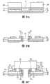
以下参照图2A至图2E的一系列剖面图来说明集成电路封装体的制作方法的一个实施例。An embodiment of the manufacturing method of the integrated circuit package is described below with reference to a series of cross-sectional views of FIGS. 2A to 2E .
参照图2A,其示出在本发明优选实施例中,形成集成电路封装体的起始步骤。首先,提供基板2。优选的,基板2可以是聚亚酰胺基板。随后,在基板2上分别形成导电材料层4和36。导电材料层4和36可以是一般常用的材料,例如在一个实施例中,导电材料层4和36包括铜或铜合金,然而,其它如金、银或铝也可使用。在一个实施例中,导电材料层4和36可通过贴附或黏着等方式,分别形成于基板2的上表面和下表面。然而,也可利用电镀工艺将导电材料层4和36分别形成于基板2的上、下表面。或是在第一导电材料层上涂布绝缘层,待此绝缘层固化后即形成基板;再于基板的另一面利用电镀或是黏着、贴附等方法形成第二导电材料层(图未显示)。需注意的是,导电材料层4和36可为相同材料,也可为不同的材料。Referring to FIG. 2A, which illustrates the initial steps in forming an integrated circuit package in a preferred embodiment of the present invention. First, a
接着,如图2B所示,形成图案化光阻层80于基板2上表面的导电材料层4的上面,由此作为蚀刻掩膜。Next, as shown in FIG. 2B , a patterned
参照图2C,随后利用镭射钻孔、蚀刻或其组合,移除部分的基板2和导电材料层4,因而形成开口86,且从开口86底部暴露出部分的导电材料层36。其中,位于基板2a下表面的导电材料层36可作为第一散热层。Referring to FIG. 2C , a portion of the
然后,参照图2D,在开口86中形成第二散热层39,其中第二散热层39高于导电材料层4。在本实施例中,第二散热层39可利用电镀法、物理气相沉积法(PVD)或化学气相沉积法(CVD)形成。Then, referring to FIG. 2D , the second
参照图2E,其示出移除图案化光阻层80后,再利用已知的微影工艺和蚀刻技术以图案化导电材料层4,由此形成多个导线4a。一般而言,导电材料层4的图案化工艺包括如下步骤:首先,在导电材料层4上形成图案化光阻层(图未显示),然后再施以蚀刻工艺,移除导电材料层4上未被图案化光阻层覆盖的部分,而此导电材料层4的剩余部分则形成多个导线4a。随后实施印刷工艺,例如网板印刷,在导线4a的外部形成绝缘层8,由此保护导线4a。在本实施例中,绝缘层8是由环氧树脂(epoxy resin)形成。Referring to FIG. 2E , it shows that after removing the patterned
接着,如图2F所示,提供芯片28,设置于基板2的上表面的上方,因而在两者之间形成腔室。然后,进一步在芯片28朝向基板2的上表面的一侧形成多个接合垫(bonding pad)26,其中这些接合垫26中的至少一个与上述导线4a中的一个电性连接。在一实施例中,接合垫26可利用物理气相沉积、化学气相沉积、电镀或其组合形成。上述导电材料层36及第二散热层39可构成散热层,由此将半导体芯片28的热通过导电材料层36和第二散热层39传递至集成电路封装体外部,其中第二散热层39从开口86底部的导电材料层36延伸至腔室内并与芯片28接触。Next, as shown in FIG. 2F , a
随后,将具有多个接合垫(bonding pad)26的半导体芯片28接合于基板2a上,且至少一个接合垫26与上述导线4a中的一个电性连接。最后再填入树脂32于腔室内以密封半导体芯片28和基板2a之间的散热层39。Subsequently, a
参照图2G,其示出了另一实施例,在本例中,可通过缩短电镀时间或光罩图案的特殊设计等手段,形成散热层84从开口86底部的导电材料层36延伸至腔室内,且在腔室内形成一个与半导体芯片28接触的较小面积的散热层84,代替上述形成于腔室中的较大面积的散热层39以节省制造成本。Referring to FIG. 2G , it shows another embodiment. In this example, the
图3A至图3E为另一实施例,示出了一集成电路封装体的制作方法。3A to 3E are another embodiment, showing a manufacturing method of an integrated circuit package.
参照图3A,其示出了在另一实施例中,形成集成电路封装体的起始步骤。首先,提供基板2。优选的,基板2可以是聚亚酰胺基板。随后,形成导电材料层4于基板2上。此导电材料层4可以是一般常用的材料,例如在一个实施例中,导电材料层4包括铜或铜合金,然而,其它如金、银或铝也可使用。在本实施例中,导电材料层4可利用物理气相沉积法、化学气相沉积法、电镀法或其组合形成。Referring to FIG. 3A , it illustrates the initial steps of forming an integrated circuit package in another embodiment. First, a
接着,参考图3B,其示出可利用已知的微影工艺和蚀刻技术以图案化导电材料层4,由此形成多个导线4a。Next, referring to FIG. 3B , it shows that the
参照图3C,随后可通过例如镭射钻孔、蚀刻或其组合,形成至少一个孔洞6于基板2中且贯穿基板2,因而形成基板2a。Referring to FIG. 3C , at least one
接着,如图3D所示,将具有多个接合垫26和第一散热层38的半导体芯片28接合于基板2a上,且至少一个接合垫26与上述导线4a之一电性连接,因而在半导体芯片28和基板2a之间形成腔室9。在一个实施例中,上述接合垫26可利用物理气相沉积、化学气相沉积、电镀或其组合形成。随后实施印刷工艺,例如网板印刷,在导线4a的外部形成绝缘层8,由此保护导线4a。Next, as shown in FIG. 3D, a
参照图3E,直接利用精密对位技术,将具有突出结构的第二散热层46,对准孔洞6后与基板2a、芯片28黏贴组合后,最后再填入树脂32于腔室9内以密封半导体芯片28和基板2a之间的第一散热层38和第二散热层46。Referring to FIG. 3E , the precision alignment technology is directly used to align the second
然后参照图3D和图3F,其示出在另一实施例中,可通过增加电镀时间,于半导体芯片28上形成较厚的第一散热层34,其中第一散热层34穿过腔室9及孔洞6并与大气接触,以提供传递热量的散热效果。值得注意的是,由于散热层38仅形成于孔洞6和腔室9内,但并未形成于基板2a的下表面,因此相比于图2F的实施例,本实施例的集成电路封装体的制作方法是针对单层导电材料的电路板基材,故相对前述具有双层导电材料的电路板基材的制作方法而言,具有较低的制造成本的优点。3D and FIG. 3F, it shows that in another embodiment, a thicker first
图4A至图4D为一优选实施例,其示出了集成电路封装体的制作方法。4A to 4D are a preferred embodiment, which illustrate the fabrication method of the integrated circuit package.
参照图4A,首先提供一个与图2C相同结构的组件,由于其制作方式与图2A至图2C的实施例相同,故在此不再赘述。Referring to FIG. 4A , firstly, a component with the same structure as in FIG. 2C is provided. Since its manufacturing method is the same as that of the embodiment in FIG. 2A to FIG. 2C , it will not be repeated here.
随后,参照图4B,形成第二散热层70于开口86中,且第二散热层70实质上与导电材料层4’等高。在本实施例中,第二散热层70可利用电镀法、物理气相沉积法(PVD)或化学气相沉积法(CVD)形成。Subsequently, referring to FIG. 4B , a second
参照图4C,其示出移除图案化光阻层80之后,再利用已知的微影工艺和蚀刻技术以图案化导电材料层4’,因而形成多个导线4a。Referring to FIG. 4C , it shows that after the patterned
接着,如图4D所示,提供具有与图3D相同结构的芯片28,设置于基板2a的上表面的上方。随后,利用黏着材料将芯片28接合于基板2a上,其中第一散热层38与上述第二散热层70接触且接合垫26中的至少一个与上述导线4a之一电性连接。随后实施印刷工艺,例如网板印刷,在导线4a的外部形成绝缘层8,由此保护导线4a。最后再填入树脂32于腔室内以密封半导体芯片28和基板2a之间的第一散热层38与第二散热层70。因此,半导体芯片28操作时所产生的热可通过第一散热层38、第二散热层70、以及导电材料层36传递至集成电路封装体外部。Next, as shown in FIG. 4D , a
参照图4E,其示出了另一实施例,在本实施例中,可通过缩短电镀或物理/化学气相沉积时间,或光罩图案的特殊设计,在半导体芯片28上形成一个较小面积的散热层42,代替图4D的实施例中位于半导体芯片28上的较大面积的第一散热层38以节省制造成本。另外,也可通过缩短电镀时间,形成较小面积的第二散热层71,代替图4D的实施例中位于导电材料层36上的较大面积的第二散热层70以进一步节省制造成本。Referring to Fig. 4E, it shows another embodiment, in this embodiment, can form a smaller area on the
图5A至图5C为另一实施例,示出了一集成电路封装体的制作方法。5A to 5C are another embodiment, showing a manufacturing method of an integrated circuit package.
参照图5A,首先提供一个与图4B相同结构的组件,由于其制作方式与图2A至图2C及图4B的实施例相同,故在此不再赘述。同样地,形成于导电材料层5上的第二散热层75与位于基板3a上的导电材料层5’等高,其中导电材料层5可用作为第一散热材料。Referring to FIG. 5A , a component with the same structure as that in FIG. 4B is firstly provided. Since its manufacturing method is the same as the embodiment in FIGS. 2A to 2C and FIG. 4B , it will not be repeated here. Likewise, the second
随后,参考图5B,其示出了移除图案化光阻层90之后,再利用已知的微影工艺和蚀刻技术以图案化导电材料层5’,由此形成多个导线5a。接着,再利用镭射钻孔或蚀刻工艺,移除一部分的第二散热层75和导电材料层5,以形成开口87、导电材料层5b和多个分开的第二散热层77,其中这些分开的第二散热层77与导线5a及导电材料层5b连接。Subsequently, referring to FIG. 5B , it shows that after removing the patterned
如图5C所示,随后将一个具有多个接合垫26的半导体芯片28接合于基板3a上,其中至少一个接合垫26与导线5a中的一个电性连接,因而在半导体芯片28和基板3a之间形成腔室。同样地,上述接合垫26可利用物理气相沉积、化学气相沉积、电镀或其组合形成。接着,利用印刷工艺,例如网板印刷,在导线5a外部形成绝缘层8,由此保护导线5a。最后再填入树脂32于腔室内以密封半导体芯片28和基板3a之间的导线5a。As shown in FIG. 5C, a
参照图5D,其示出在一实施例中,散热层50从基板3a下表面的导线5b穿过孔洞且延伸至基板3a上表面,并完全覆盖孔洞。本实施例与第4E图的实施的差别在于:散热层50除了与接合垫26接触之外,进一步与形成于半导体芯片28上的接合垫27接触,因而可提供相对较高的散热效率。其中,接合垫27的长度比接合垫26长,且利用与接合垫26实质相同的方法形成,并与接合垫26相邻。Referring to FIG. 5D , it shows that in one embodiment, the
在另一实施例中,如图5E所示,其示出散热层52从基板3a的下表面穿过位于半导体芯片28外侧的孔洞,再向内侧延伸至基板3a的上表面,且与半导体芯片28上的接合垫26接触,因此,半导体芯片28操作时所产生的热,可通过散热层52传递至集成电路封装体外部。In another embodiment, as shown in FIG. 5E , it shows that the
以下结合图6至图10的结构剖面图来说明集成电路封装体的结构的其它实施例。Other embodiments of the structure of the integrated circuit package will be described below with reference to the structural sectional views of FIGS. 6 to 10 .
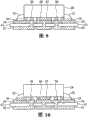
参照图6,其示出散热层54从基板60的下表面穿过孔洞延伸至基板60上表面,且和位于基板60上表面的导线56接触。由于在此实施例中,散热层54和接合垫26及半导体芯片28之间相隔一既定距离,因此半导体芯片28操作时所产生的热,依序透过树脂32和散热层54传递至集成电路封装体外部。Referring to FIG. 6 , it shows that the
如图7所示,在另一实施例中,在具有多个孔洞的基板61上形成第一散热层62和一个与第一散热层62相邻的第二散热层63,且分别填入不同的孔洞内。其中,第一散热层62和接合垫26连接,而第二散热层63则与接合垫26及半导体芯片28之间相隔一既定距离。在此实施例中,由于第一散热层62和接合垫26接触,因此,相比于图6的实施例,本实施例可进一步提高集成电路封装体的散热效率。As shown in FIG. 7, in another embodiment, a first
如图8所示,其示出在一个优选的实施例中,可通过增加电镀时间,将图7的实施例中的第二散热层63从腔室9延伸至半导体芯片28上,而形成第三散热层64,以提升集成电路封装体的散热效率。As shown in FIG. 8, it shows that in a preferred embodiment, the second
参照图9,其示出在一实施例中,第一散热层62和第二散热层66分别与接合垫26及第三散热层65连接。其中,第三散热层65形成于半导体芯片28上且和接合垫26相邻。因此,半导体芯片28操作时所产生的热,可分别透过接合垫26和第一散热层62,以及第三散热层65和第二散热层66传递至集成电路封装体外部。Referring to FIG. 9 , it shows that in one embodiment, the first
参照图10,其示出也可通过缩短电镀或物理/化学气相沉积时间,或光罩图案的特殊设计,形成具有较小面积的散热层67来代替图9中的第三散热层65,以节省集成电路封装体的制造成本。Referring to FIG. 10, it shows that the
上述实施例具有许多优点,例如在图6至图10的实施例中,当半导体芯片28操作时,可分别通过接合垫26之一和导线56,以及接合垫26中的另一个和第一散热层62将电子讯号传递至基板61上。也就是,利用这些实施例,可在相同尺寸的封装体中制作多重走线,由此提高电子讯号的传输效率。而且,由于这些走线同时兼具散热功能,因此,利用这些实施例还可同时提升封装体的散热效率。The above-described embodiment has many advantages. For example, in the embodiment of FIGS.
这些实施例的另一优点在于,由于散热层可以是与基板表面上的导线相同材质,因此,不需要额外的材料成本,即可达到改善集成电路封装体的散热效率。Another advantage of these embodiments is that since the heat dissipation layer can be made of the same material as the wires on the surface of the substrate, the heat dissipation efficiency of the integrated circuit package can be improved without additional material costs.
虽然本发明已经以优选实施例披露如上,但其并非用以限定本发明,任何本领域的技术人员,在不脱离本发明的精神和范围内,可作更改和修改,因此本发明的保护范围当以所附权利要求为准。Although the present invention has been disclosed as above with preferred embodiments, it is not intended to limit the present invention, any skilled in the art can make changes and modifications without departing from the spirit and scope of the present invention, so the protection scope of the present invention The appended claims shall prevail.
主要组件符号说明Explanation of main component symbols
封装基板10 半导体芯片12Package substrate 10 Semiconductor chip 12
黏着层14 锡球16Adhesive layer 14 Solder ball 16
印刷电路板18 封装树脂20、Printed circuit board 18 Packaging resin 20,
基板2 基板2a
基板3 基板3aSubstrate 3
基板6a、60 基板61
导电材料层4 导电材料层4’
导电材料层5 导电材料层5’
导电材料层36 导线4a
导线5a 导线56
孔洞6 绝缘层8
腔室9 接合垫26
接合垫27 树脂32Bonding Pad 27
散热层42 散热层50
散热层52 散热层54
散热层67 散热层84
第一散热层34 第一散热层38The first
第一散热层62 第二散热层39The first
第二散热层46 第二散热层63The second
第二散热层70 第二散热层71The second
第二散热层75 分开的第二散热层77Second
导电材料层5b 第三散热层64
第三散热层65 图案化光阻层80The third
图案化光阻层90 开口86Patterned
开口87opening 87
Claims (24)
Translated fromChinesePriority Applications (1)
| Application Number | Priority Date | Filing Date | Title |
|---|---|---|---|
| CN2008100041699ACN101494205B (en) | 2008-01-23 | 2008-01-23 | Integrated circuit package and manufacturing method thereof |
Applications Claiming Priority (1)
| Application Number | Priority Date | Filing Date | Title |
|---|---|---|---|
| CN2008100041699ACN101494205B (en) | 2008-01-23 | 2008-01-23 | Integrated circuit package and manufacturing method thereof |
Publications (2)
| Publication Number | Publication Date |
|---|---|
| CN101494205A CN101494205A (en) | 2009-07-29 |
| CN101494205Btrue CN101494205B (en) | 2011-02-02 |
Family
ID=40924715
Family Applications (1)
| Application Number | Title | Priority Date | Filing Date |
|---|---|---|---|
| CN2008100041699AActiveCN101494205B (en) | 2008-01-23 | 2008-01-23 | Integrated circuit package and manufacturing method thereof |
Country Status (1)
| Country | Link |
|---|---|
| CN (1) | CN101494205B (en) |
Citations (4)
| Publication number | Priority date | Publication date | Assignee | Title |
|---|---|---|---|---|
| CN1199927A (en)* | 1997-05-17 | 1998-11-25 | 现代电子产业株式会社 | Encapsulated integrated circuit component and its producing method |
| US6130477A (en)* | 1999-03-17 | 2000-10-10 | Chen; Tsung-Chieh | Thin enhanced TAB BGA package having improved heat dissipation |
| US6265771B1 (en)* | 1999-01-27 | 2001-07-24 | International Business Machines Corporation | Dual chip with heat sink |
| CN1773698A (en)* | 2004-09-29 | 2006-05-17 | 美国博通公司 | Die down ball grid array packages and method for making same |
- 2008
- 2008-01-23CNCN2008100041699Apatent/CN101494205B/enactiveActive
Patent Citations (4)
| Publication number | Priority date | Publication date | Assignee | Title |
|---|---|---|---|---|
| CN1199927A (en)* | 1997-05-17 | 1998-11-25 | 现代电子产业株式会社 | Encapsulated integrated circuit component and its producing method |
| US6265771B1 (en)* | 1999-01-27 | 2001-07-24 | International Business Machines Corporation | Dual chip with heat sink |
| US6130477A (en)* | 1999-03-17 | 2000-10-10 | Chen; Tsung-Chieh | Thin enhanced TAB BGA package having improved heat dissipation |
| CN1773698A (en)* | 2004-09-29 | 2006-05-17 | 美国博通公司 | Die down ball grid array packages and method for making same |
Also Published As
| Publication number | Publication date |
|---|---|
| CN101494205A (en) | 2009-07-29 |
Similar Documents
| Publication | Publication Date | Title |
|---|---|---|
| US10460958B2 (en) | Method of manufacturing embedded packaging with preformed vias | |
| US6395582B1 (en) | Methods for forming ground vias in semiconductor packages | |
| US7839649B2 (en) | Circuit board structure having embedded semiconductor element and fabrication method thereof | |
| CN100417310C (en) | Printed circuit board with heat dissipating element, its manufacturing method and device containing it | |
| TWI402954B (en) | Assembly board and semiconductor module | |
| US20120199955A1 (en) | Package carrier and manufacturing method thereof | |
| US20030193096A1 (en) | Wafer-level package with a cavity and fabricating method thereof | |
| TWI628761B (en) | A stack frame for electrical connections and the method to fabricate thereof | |
| CN103378014A (en) | Package carrier and method for manufacturing the same | |
| CN112054006A (en) | Semiconductor device package and method of manufacturing the same | |
| JPH11354669A (en) | Ball grid array type semiconductor package and manufacture thereof | |
| JP2008218979A (en) | Electronic packaging and manufacturing method thereof | |
| WO2014074933A2 (en) | Microelectronic assembly with thermally and electrically conductive underfill | |
| US20090115036A1 (en) | Semiconductor chip package having metal bump and method of fabricating same | |
| CN103400810A (en) | Semiconductor chip laminating and packaging structure and manufacturing method thereof | |
| TWI380419B (en) | Integrated circuit package and the method for fabricating thereof | |
| US6432748B1 (en) | Substrate structure for semiconductor package and manufacturing method thereof | |
| TWI395318B (en) | Thin stack package using embedded-type chip carrier | |
| CN104167369B (en) | Manufacturing method of chip packaging structure | |
| KR100693168B1 (en) | Printed Circuit Board and Manufacturing Method | |
| KR101092945B1 (en) | Package substrate, electronic component package having the same and method of manufacturing package substrate | |
| KR100963201B1 (en) | Chip embedded substrate and manufacturing method thereof | |
| CN101494205B (en) | Integrated circuit package and manufacturing method thereof | |
| KR101152822B1 (en) | Fabricating method for wafer | |
| KR20070098037A (en) | Packaged printed circuit board and its manufacturing method |
Legal Events
| Date | Code | Title | Description |
|---|---|---|---|
| C06 | Publication | ||
| PB01 | Publication | ||
| C10 | Entry into substantive examination | ||
| SE01 | Entry into force of request for substantive examination | ||
| C14 | Grant of patent or utility model | ||
| GR01 | Patent grant |