CN101494112B - A method for forming coil inductance - Google Patents
A method for forming coil inductanceDownload PDFInfo
- Publication number
- CN101494112B CN101494112BCN2008100897098ACN200810089709ACN101494112BCN 101494112 BCN101494112 BCN 101494112BCN 2008100897098 ACN2008100897098 ACN 2008100897098ACN 200810089709 ACN200810089709 ACN 200810089709ACN 101494112 BCN101494112 BCN 101494112B
- Authority
- CN
- China
- Prior art keywords
- dielectric layer
- conductive structure
- formation method
- coil
- conductive
- Prior art date
- Legal status (The legal status is an assumption and is not a legal conclusion. Google has not performed a legal analysis and makes no representation as to the accuracy of the status listed.)
- Active
Links
- 238000000034methodMethods0.000titleclaimsabstractdescription48
- 230000005294ferromagnetic effectEffects0.000claimsdescription33
- 239000000758substrateSubstances0.000claimsdescription20
- 230000015572biosynthetic processEffects0.000claimsdescription17
- 238000009713electroplatingMethods0.000claimsdescription14
- 229910052710siliconInorganic materials0.000claimsdescription9
- 239000010703siliconSubstances0.000claimsdescription9
- XEEYBQQBJWHFJM-UHFFFAOYSA-NIronChemical compound[Fe]XEEYBQQBJWHFJM-UHFFFAOYSA-N0.000claimsdescription6
- PXHVJJICTQNCMI-UHFFFAOYSA-NNickelChemical compound[Ni]PXHVJJICTQNCMI-UHFFFAOYSA-N0.000claimsdescription6
- XUIMIQQOPSSXEZ-UHFFFAOYSA-NSiliconChemical compound[Si]XUIMIQQOPSSXEZ-UHFFFAOYSA-N0.000claimsdescription6
- 238000001459lithographyMethods0.000claimsdescription6
- 239000004952PolyamideSubstances0.000claimsdescription5
- 229920002647polyamidePolymers0.000claimsdescription5
- 229910017052cobaltInorganic materials0.000claimsdescription3
- 239000010941cobaltSubstances0.000claimsdescription3
- GUTLYIVDDKVIGB-UHFFFAOYSA-Ncobalt atomChemical compound[Co]GUTLYIVDDKVIGB-UHFFFAOYSA-N0.000claimsdescription3
- 229910052742ironInorganic materials0.000claimsdescription3
- 229910052759nickelInorganic materials0.000claimsdescription3
- 238000005530etchingMethods0.000claimsdescription2
- 150000003376siliconChemical class0.000claims3
- 150000002118epoxidesChemical class0.000claims2
- 229920002120photoresistant polymerPolymers0.000description27
- 239000002184metalSubstances0.000description14
- 229910052751metalInorganic materials0.000description14
- 230000008569processEffects0.000description11
- 230000005684electric fieldEffects0.000description4
- 230000005291magnetic effectEffects0.000description4
- 230000035699permeabilityEffects0.000description4
- RYGMFSIKBFXOCR-UHFFFAOYSA-NCopperChemical compound[Cu]RYGMFSIKBFXOCR-UHFFFAOYSA-N0.000description3
- 239000004593EpoxySubstances0.000description3
- 229910052802copperInorganic materials0.000description3
- 239000010949copperSubstances0.000description3
- 238000004519manufacturing processMethods0.000description3
- 239000000463materialSubstances0.000description3
- 238000002161passivationMethods0.000description3
- 238000000059patterningMethods0.000description3
- 238000004364calculation methodMethods0.000description2
- 230000008859changeEffects0.000description2
- 239000004020conductorSubstances0.000description2
- 239000013078crystalSubstances0.000description2
- 238000002513implantationMethods0.000description2
- 238000012986modificationMethods0.000description2
- 230000004048modificationEffects0.000description2
- 239000003990capacitorSubstances0.000description1
- 238000000151depositionMethods0.000description1
- 238000009795derivationMethods0.000description1
- 239000007943implantSubstances0.000description1
- 230000001939inductive effectEffects0.000description1
- 239000000615nonconductorSubstances0.000description1
- 239000002245particleSubstances0.000description1
- 238000007747platingMethods0.000description1
- 238000007517polishing processMethods0.000description1
- 238000000926separation methodMethods0.000description1
Images


Classifications
- H—ELECTRICITY
- H01—ELECTRIC ELEMENTS
- H01F—MAGNETS; INDUCTANCES; TRANSFORMERS; SELECTION OF MATERIALS FOR THEIR MAGNETIC PROPERTIES
- H01F41/00—Apparatus or processes specially adapted for manufacturing or assembling magnets, inductances or transformers; Apparatus or processes specially adapted for manufacturing materials characterised by their magnetic properties
- H01F41/02—Apparatus or processes specially adapted for manufacturing or assembling magnets, inductances or transformers; Apparatus or processes specially adapted for manufacturing materials characterised by their magnetic properties for manufacturing cores, coils, or magnets
- H01F41/04—Apparatus or processes specially adapted for manufacturing or assembling magnets, inductances or transformers; Apparatus or processes specially adapted for manufacturing materials characterised by their magnetic properties for manufacturing cores, coils, or magnets for manufacturing coils
- H01F41/041—Printed circuit coils
- H01F41/046—Printed circuit coils structurally combined with ferromagnetic material
- H—ELECTRICITY
- H01—ELECTRIC ELEMENTS
- H01F—MAGNETS; INDUCTANCES; TRANSFORMERS; SELECTION OF MATERIALS FOR THEIR MAGNETIC PROPERTIES
- H01F17/00—Fixed inductances of the signal type
- H01F17/0006—Printed inductances
- H01F17/0013—Printed inductances with stacked layers
- H—ELECTRICITY
- H01—ELECTRIC ELEMENTS
- H01F—MAGNETS; INDUCTANCES; TRANSFORMERS; SELECTION OF MATERIALS FOR THEIR MAGNETIC PROPERTIES
- H01F17/00—Fixed inductances of the signal type
- H01F17/0006—Printed inductances
- H01F17/0033—Printed inductances with the coil helically wound around a magnetic core
- H—ELECTRICITY
- H01—ELECTRIC ELEMENTS
- H01F—MAGNETS; INDUCTANCES; TRANSFORMERS; SELECTION OF MATERIALS FOR THEIR MAGNETIC PROPERTIES
- H01F17/00—Fixed inductances of the signal type
- H01F17/0006—Printed inductances
- H01F2017/0086—Printed inductances on semiconductor substrate
- Y—GENERAL TAGGING OF NEW TECHNOLOGICAL DEVELOPMENTS; GENERAL TAGGING OF CROSS-SECTIONAL TECHNOLOGIES SPANNING OVER SEVERAL SECTIONS OF THE IPC; TECHNICAL SUBJECTS COVERED BY FORMER USPC CROSS-REFERENCE ART COLLECTIONS [XRACs] AND DIGESTS
- Y10—TECHNICAL SUBJECTS COVERED BY FORMER USPC
- Y10T—TECHNICAL SUBJECTS COVERED BY FORMER US CLASSIFICATION
- Y10T29/00—Metal working
- Y10T29/49—Method of mechanical manufacture
- Y10T29/49002—Electrical device making
- Y10T29/4902—Electromagnet, transformer or inductor
Landscapes
- Engineering & Computer Science (AREA)
- Power Engineering (AREA)
- Manufacturing & Machinery (AREA)
- Coils Or Transformers For Communication (AREA)
- Manufacturing Cores, Coils, And Magnets (AREA)
Abstract
Translated fromChinese
Description
Translated fromChinese技术领域technical field
本发明涉及一种线圈电感的形成方法,且特别涉及一种减少能量损失的线圈电感的形成方法。The invention relates to a method for forming coil inductance, and in particular to a method for forming coil inductance that reduces energy loss.
背景技术Background technique
传统的电感制造方式是利用导电材料在硅衬底(substrate)上形成线圈。线圈可为形成于介电膜上的螺旋状结构。如图1的螺旋状电感的俯视图所示,传统的螺旋状电感为螺旋状结构的电感线圈102平放在衬底表面104上,线圈102的两个端点106及108分别电性连接于一转接垫(transfer pad)。流经电感线圈102的电流产生感应系数L及质量因子Q。同时,也会产生流过衬底,称为涡流(eddy current)的微小电流。The traditional manufacturing method of inductors is to use conductive materials to form coils on silicon substrates. The coil may be a helical structure formed on a dielectric film. As shown in the top view of the spiral inductor in FIG. 1 , the traditional spiral inductor is an
涡流可视为在衬底上耗费的功率,并产生了电感的能量损失,降低质量因子Q,即电感的性能。质量因子Q定义为电感内储存的能量与电感的功率损耗的比值。因此,当涡流产生的功率损耗变大,更多的质量因子Q将因此降低。因此,制造硅衬底上的电感的挑战常来自于如何降低涡流的产生。The eddy currents can be seen as power dissipated on the substrate and cause energy losses in the inductor, reducing the quality factor Q, which is the performance of the inductor. The quality factor Q is defined as the ratio of the energy stored in the inductor to the power loss of the inductor. Therefore, when the power loss generated by eddy currents becomes larger, more quality factor Q will be reduced accordingly. Therefore, the challenge of manufacturing inductors on silicon substrates often comes from how to reduce the generation of eddy currents.
因此,如何设计一个能减少涡流,进而使质量因子提高的电感结构,为本领域亟待解决的问题。Therefore, how to design an inductor structure that can reduce eddy currents and improve the quality factor is an urgent problem to be solved in this field.
发明内容Contents of the invention
本发明所要解决的技术问题在于提供一种线圈电感的形成方法,以获得涡流减少、质量因子提高的电感结构。The technical problem to be solved by the present invention is to provide a method for forming coil inductance, so as to obtain an inductance structure with reduced eddy current and improved quality factor.
为达到上述目的,本发明提供一种线圈电感的形成方法,其中该线圈电感为螺线管状的结构,该形成方法包含下列步骤:形成多个底部导电结构于第一电介质层上;形成多对侧部导电结构,其中每对侧部导电结构分别直立形成于每个底部导电结构的第一端点及第二端点上;形成第二电介质层于该第一电介质层上,该第二电介质层覆盖该底部导电结构及侧部导电结构;以及形成多个顶部导电结构于该第二电介质层上,其中每个顶部导电结构电性连接每一对侧部导电结构;该底部导电结构、侧部导电结构及顶部导电结构共同形成该线圈电感结构。In order to achieve the above object, the present invention provides a method for forming a coil inductance, wherein the coil inductance is a solenoid-shaped structure, and the forming method includes the following steps: forming a plurality of bottom conductive structures on the first dielectric layer; forming a plurality of pairs of The side conductive structures, wherein each pair of side conductive structures are formed upright on the first end point and the second end point of each bottom conductive structure; a second dielectric layer is formed on the first dielectric layer, and the second dielectric layer covering the bottom conductive structure and side conductive structures; and forming a plurality of top conductive structures on the second dielectric layer, wherein each top conductive structure is electrically connected to each pair of side conductive structures; the bottom conductive structure, the side conductive structures The conductive structure and the top conductive structure jointly form the coil inductance structure.
为达到上述目的,本发明还提供了另一种线圈电感的形成方法,其中该线圈电感为螺旋状的结构,该形成方法包含下列步骤:形成光刻胶层于第一电介质层上;图案化该光刻胶层以形成螺旋状图案;根据该螺旋状图案电镀(plating)导电螺旋状结构于该第一电介质层上;移除该光刻胶层;以及形成铁磁芯(ferromagnetic core)于该导电螺旋状结构的中心。In order to achieve the above object, the present invention also provides another method for forming a coil inductance, wherein the coil inductance is a spiral structure, and the method for forming comprises the following steps: forming a photoresist layer on the first dielectric layer; patterning the photoresist layer to form a helical pattern; electroplating (plating) a conductive helical structure on the first dielectric layer according to the helical pattern; removing the photoresist layer; and forming a ferromagnetic core (ferromagnetic core) on the first dielectric layer The center of the conductive helix.
虽然本发明已经以一较佳实施例揭露如上,然其并非用以限定本发明,任何本领域的技术人员,在不脱离本发明的精神和范围内,当可作各种的改变与变形,因此本发明的保护范围当视后附的权利要求书所界定的为准。Although the present invention has been disclosed above with a preferred embodiment, it is not intended to limit the present invention. Any person skilled in the art may make various changes and modifications without departing from the spirit and scope of the present invention. Therefore, the scope of protection of the present invention should be defined by the appended claims.
为让本发明的上述和具它目的、特征、优点与实施例能更明显易懂,下面结合附图详细说明。In order to make the above and other objects, features, advantages and embodiments of the present invention more comprehensible, the following detailed descriptions are given in conjunction with the accompanying drawings.
附图说明Description of drawings
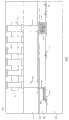
图1是现有技术中的螺旋状电感的俯视图;1 is a top view of a spiral inductor in the prior art;
图2为通过本发明的第一实施例的形成方法所制造的线圈电感的立体图;Fig. 2 is the perspective view of the coil inductance manufactured by the forming method of the first embodiment of the present invention;
图2A-2F为线圈电感在本发明的第一实施例的形成方法的各步骤后,沿A线的剖面图;2A-2F are cross-sectional views along line A of the coil inductance after each step of the forming method of the first embodiment of the present invention;
图3为通过本发明的第二实施例的形成方法所制造的线圈电感的立体图;3 is a perspective view of a coil inductor manufactured by a forming method according to a second embodiment of the present invention;
图3A-3G为具有铁磁芯的线圈电感在本发明的第二实施例的形成方法的各步骤后,沿B线的剖面图;3A-3G are cross-sectional views along line B after each step of the forming method of the coil inductor with a ferromagnetic core in the second embodiment of the present invention;
图4为在本发明的第三实施例中,具有铁磁芯的螺旋状线圈电感的俯视图;4 is a top view of a helical coil inductor with a ferromagnetic core in a third embodiment of the present invention;
图4A-4F为线圈电感在本发明的第三实施例的形成方法的各步骤后,沿C线的剖面图;以及4A-4F are cross-sectional views along line C of the coil inductance after each step of the forming method of the third embodiment of the present invention; and
图5为集成电路芯片的剖面图。FIG. 5 is a cross-sectional view of an integrated circuit chip.
【主要器件符号说明】【Description of main device symbols】
102:电感线圈 104:衬底表面102: Inductance coil 104: Substrate surface
106、108:端点 200:线圈电感106, 108: endpoint 200: coil inductance
202:第一电介质层 204:导电线圈电感结构202: The first dielectric layer 204: Conductive coil inductance structure
206:衬底 208:终端接点206: Substrate 208: Terminal contact
210:导电连接件 212:底部导电结构210: Conductive connector 212: Bottom conductive structure
214:侧部导电结构 218:第二电介质层214: Side conductive structure 218: Second dielectric layer
220:顶部导电结构 302:铁磁芯220: Top conductive structure 302: Ferromagnetic core
304:沟槽 306:光刻胶层304: Groove 306: Photoresist layer
308:侧部导电结构延伸部 310:第三电介质层308: Side conductive structure extension 310: Third dielectric layer
312:光刻胶层 402:光刻胶312: photoresist layer 402: photoresist
404:导电螺旋层 406:光刻胶层404: Conductive spiral layer 406: Photoresist layer
408:铁磁芯 500:集成电路芯片408: Ferromagnetic core 500: Integrated circuit chip
502:晶体管层 504:金属层502: Transistor layer 504: Metal layer
506:金属层间电介质层 508:连接点506: Inter-metal dielectric layer 508: Connection point
510:钝化层 512:电介质层510: Passivation layer 512: Dielectric layer
514:导电线圈结构 516:铁磁芯514: Conductive coil structure 516: Ferromagnetic core
518:晶体管 520:导电连接件518: Transistor 520: Conductive connector
具体实施方式Detailed ways
一般来说,接近电感的材料所感受到的电场强度,与电感及材料间的距离成反比。根据麦克斯韦方程式(Maxwell’s equations),可以导出电感外的电场与其距离成反比。此关系在电感在低频率、电场计算点在非导体内时可以被轻易导出,然而当电感高频率工作且电场计算点在如硅衬底的导体内时,推导过程将复杂许多。然而,不论工作频率及所在材料是否为导电材料,当一个物体离带电粒子愈远,物体所感受到的磁场愈小。因此,衬底内的涡流将可通过增加线圈电感及衬底间的距离而减少。In general, the electric field strength felt by a material close to the inductor is inversely proportional to the distance between the inductor and the material. According to Maxwell's equations, it can be derived that the electric field outside the inductor is inversely proportional to its distance. This relationship can be easily derived when the inductor operates at low frequencies and the calculation point of the electric field is in a non-conductor. However, when the inductor operates at high frequency and the calculation point of the electric field is in a conductor such as a silicon substrate, the derivation process is much more complicated. However, regardless of the operating frequency and whether the material is conductive or not, the farther an object is from the charged particles, the smaller the magnetic field felt by the object. Therefore, the eddy current in the substrate will be reduced by increasing the coil inductance and the distance between the substrates.
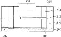
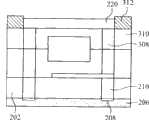
请参考图2,为通过本发明的第一实施例的形成方法所制造的线圈电感的立体图。在本实施例中,线圈电感200可为借由第一电介质层202而与衬底206间隔一距离的螺线管状的结构204。在图2A中,示出线圈电感在形成方法的第一个步骤后,沿着A线的剖面图。在第一步骤中,提供具有两个终端接点208的硅衬底206。两个终端接点208为两个金属接点。形成在两个终端接点208上的是两个导电连接件210,以将终端接点208电性连接到导电线圈电感结构204。两个导电连接件210由平版印刷术(lithography)工艺及电镀工艺形成。其中电镀工艺可为铜电镀工艺。第一电介质层202接着形成于衬底206上方并覆盖导电连接件210。第一电介质层202至少具有5um的厚度,以使衬底206及导电线圈电感结构204间具有一足够的间隔距离。当第一电介质层202形成后,导电线圈电感结构204即形成于其上。其中,第一电介质层由环氧化物(epoxy)或聚酰胺(polyamide)形成。Please refer to FIG. 2 , which is a perspective view of the coil inductor manufactured by the forming method of the first embodiment of the present invention. In this embodiment, the
请参考图2B,示出线圈电感在形成方法的第二个步骤后,沿着A线的剖面图。第二步骤包含形成多个底部导电结构212于第一电介质层202上。底部导电结构212由金属,如铜,电镀于第一电介质层202上,且最外部两侧的底部导电结构212分别电性连接两个导电连接件210。对照图2,导电线圈电感结构204为截面为方形的螺线管状结构,而底部导电结构212则为导电线圈电感结构204的底侧。Please refer to FIG. 2B , which shows a cross-sectional view of the coil inductor along line A after the second step of the forming method. The second step includes forming a plurality of bottom
接着参考图2C,示出线圈电感在形成方法的第三个步骤后,沿着A线的剖面图。在第三步骤中,多对侧部导电结构214分别直立形成并电性连接每个底部导电结构212的第一端点及第二端点上。侧部导电结构214的形成过为:先通过形成一层光刻胶于第一电介质层202上,其中此光刻胶层可为干膜光刻胶层;接着,图案化光刻胶层以形成多个开孔,最后,通过金属,如铜,电镀于开孔中,以形成侧部导电结构214。对照图2,侧部导电结构214是为螺线管状结构的导电线圈电感结构204的两侧。Referring next to FIG. 2C , it shows a cross-sectional view of the coil inductor along line A after the third step of the forming method. In the third step, a plurality of pairs of side
接着参考图2D,示出线圈电感在形成方法的第四个步骤后,沿着A线的剖面图。在第四步骤中,光刻胶层被移除以曝露出侧部导电结构214及底部导电结构212。在第五步骤,如图2E所示,第二电介质层218形成在该第一电介质层202上并覆盖底部导电结构212及侧部导电结构214。第二电介质层218由环氧化物或聚酰胺形成。第二电介质层218接着通过抛光(polishing)过程而曝露出侧部导电结构214。Referring next to FIG. 2D , it shows a cross-sectional view of the coil inductor along line A after the fourth step of the forming method. In the fourth step, the photoresist layer is removed to expose the side
在最后一个步骤中,如图2F所示,形成多个顶部导电结构220在第二电介质层218上,其中每个顶部导电结构220电性连接每一对侧部导电结构214;底部导电结构212、侧部导电结构214及顶部导电结构220共同形成导电线圈电感结构204。因此,电流可由两个终端接点208流过导电线圈电感结构204。顶部导电结构220由平版印刷术工艺及电镀工艺形成,如形成一层光刻胶于第二电介质层218上,以蚀刻方式图案化光刻胶层,将金属电镀于蚀刻出的图案中,再移除光刻胶层。并且,在形成任何导电结构于第一及第二电介质层202及218上之前,电介质层上均可先形成种晶层(seed layer)(未示出)。In the last step, as shown in FIG. 2F, a plurality of top
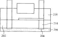
在本发明的第二实施例中,是将一铁磁芯302植入线圈电感200的中心。请参考图3,为通过本发明的第二实施例的形成方法所制造的线圈电感的立体图。通过本实施中,穿过线圈中心的铁磁芯,感应系数将因铁磁芯的磁导率而改变,质量因子Q也将因此改变。更高的质量因子,代表较少的能量损失,即由涡流所消耗的能量减少。此关系可由下列方程式表示:In the second embodiment of the present invention, a

其中L为线圈电感的感应系数,μ0为真空的磁导率,μr为铁磁芯的磁导率,N为线圈的匝数,A为线圈截面的面积,单位为平方米,l为线圈的长度,单位为米,Q为质量因子,ω为频率,R为电阻值。Among them, L is the inductance coefficient of the coil inductance, μ0 is the magnetic permeability of vacuum, μr is the magnetic permeability of the ferromagnetic core, N is the number of turns of the coil, A is the area of the coil cross section, and the unit is square meters, and l is The length of the coil in meters, Q is the quality factor, ω is the frequency, and R is the resistance value.
因此,如L值因为植入具有高磁导率的铁磁芯而增加,质量因子Q也随之增加。Therefore, as the value of L increases due to the implantation of a ferromagnetic core with high magnetic permeability, the quality factor Q also increases.
请参考图3A,示出线圈电感在第一实施例的形成方法的第五个步骤后,沿着B线的剖面图。第二电介质层218被蚀刻形成沟槽304,以进行铁磁芯302的植入。在另一实施例中,也可不形成沟槽304,而直接将铁磁芯302置于第二电介质层218的表面上。Please refer to FIG. 3A , which shows a cross-sectional view of the coil inductor along line B after the fifth step of the forming method of the first embodiment. The
请参考图3B,示出第一实施例的线圈电感200沿着B线的剖面图。光刻胶层306形成于第二电介质层218之上,接着光刻胶层306被蚀刻以曝露出沟槽304。更进一步地,铁磁芯302通过电镀过程而植入于沟槽304。铁磁芯由铁、镍或钴或其组合形成。Please refer to FIG. 3B , which shows a cross-sectional view of the
下一个步骤如图3C所示,光刻胶层306接着再被蚀刻以曝露出侧部导电结构214。多个侧部导电结构延伸部308形成于蚀刻出的空间中,以垂直地延伸侧部导电结构214,使侧部导电结构214的高度超过铁磁芯302的高度。The next step is shown in FIG. 3C , the
如图3D所示,光刻胶层306被移除。在此步骤,在光刻胶层306形成前已形成于第二电介质层218上的种晶层(未示出)也被蚀刻。As shown in FIG. 3D, the
接着请参考图3E,第三电介质层310形成在第二电介质层218上并覆盖铁磁芯302及侧部导电结构延伸部308。第三电介质层310接着进行抛光过程以曝露侧部导电结构延伸部308。第三电介质层310由环氧化物或聚酰胺形成,与第二电介质层218共同包覆住铁磁芯302。铁磁芯302因此与导电线圈电感结构204绝缘。Referring next to FIG. 3E , the third
图3F中,导电线圈电感结构204是在沉积一种晶层(未示出)于第三介电层310上,且光刻胶层312被蚀刻以电镀形成顶部导电结构220后完成。顶部导电结构220电性连接侧部导电结构延伸部308。In FIG. 3F , the conductive
最后,图3G示出本发明第二实施例的形成方法所形成的具有铁磁芯302的线圈电感200,沿B线的剖面图。光刻胶层312被移除,且种晶层(未示出)被蚀刻掉。Finally, FIG. 3G shows a cross-sectional view along line B of the
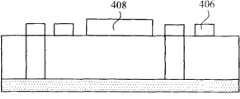
更进一步地,请参考图4,本发明的第三实施例中具有铁磁芯408的螺旋状线圈电感的俯视图。在本实施例中,形成在第一电介质层202上的是具有螺旋状的结构,该结构可通过平版印刷术工艺及电镀工艺形成。请参考图4A,示出根据本发明的第三实施例,在形成两个导电连接件210及第一电介质层202后,线圈电感400沿C线的剖面图。光刻胶层402在种晶层(未示出)沉积在第一电介质层202上后形成,并接着被蚀刻使第一电介质层202的部分上表面曝露以进行电镀工艺。Further, please refer to FIG. 4 , which is a top view of a helical coil inductor with a
接着如图4B所示,导电螺旋层404通过电镀形成于上述曝露的区域并与两个导电连接件210相电性连接。图4C中,光刻胶层402被移除。如不进行铁磁芯的工艺,此时即蚀刻种晶层而完成线圈电感的制造。然而,如欲植入铁磁芯,将再进行平版印刷术过程。Next, as shown in FIG. 4B , a conductive
请参考图4D,光刻胶层406形成于第一电介质层202上并覆盖导电螺旋层404。光刻胶层406接着被图案化以形成开口于导电螺旋层404的中心。Referring to FIG. 4D , a
接着如图4E所示,铁磁芯408被电镀入开口中。铁磁芯408由铁、镍或钴或其组合形成。最后如图4F所示,光刻胶层406被移除,且种晶层(未示出)被蚀刻而完成线圈电感的形成过程。Next, as shown in Figure 4E, a
上述的本发明的实施例提供可通过第一电介质层202及两个导电连接件210以降低衬底中的涡流的线圈电感。因此,当第一电介质层202的厚度超过5um,涡流将可大幅降低。铁磁芯也可被植入线圈电感的中心以提供高感应系数,并进一步再降低能量损耗。The embodiments of the present invention described above provide a coil inductance that reduces eddy currents in the substrate through the
图5示出形成于集成电路芯片中的线圈电感,为集成电路芯片500的剖面图,包含晶体管层502、金属层504、金属层间电介质层(inter-metal dielectric;IMD)506、连接点508、钝化层(passivation layer)510、电介质层512、导电线圈结构514及铁磁芯516。晶体管层为包含晶体管518的硅衬底。晶体管518电性连接由金属层504形成的电容,其中金属层504由金属层间电介质层506与晶体管518隔开。金属层504通过连接点508,如金属连接点及钝化层510以与嵌入于电介质层512的导电连接件520相连接。导电线圈结构514接着形成于电介质层512上,以在导电连接件520间产生电感。如前述的实施例所示,铁磁芯516可由电镀形成于导电线圈结构514的中心以增加电感的感应系数。5 shows a coil inductance formed in an integrated circuit chip, which is a cross-sectional view of an
虽然本发明已以较佳实施例揭露如上,然其并非用以限定本发明,任何本领域的技术人员,在不脱离本发明的精神和范围内,当可作各种的改变与变形,因此本发明的保护范围当视后附的权利要求书所界定的为准。Although the present invention has been disclosed above with preferred embodiments, it is not intended to limit the present invention. Any person skilled in the art may make various changes and modifications without departing from the spirit and scope of the present invention. Therefore The scope of protection of the present invention shall prevail as defined by the appended claims.
Claims (13)
Applications Claiming Priority (2)
| Application Number | Priority Date | Filing Date | Title |
|---|---|---|---|
| US12/019,688 | 2008-01-25 | ||
| US12/019,688US7666688B2 (en) | 2008-01-25 | 2008-01-25 | Method of manufacturing a coil inductor |
Publications (2)
| Publication Number | Publication Date |
|---|---|
| CN101494112A CN101494112A (en) | 2009-07-29 |
| CN101494112Btrue CN101494112B (en) | 2011-06-08 |
Family
ID=40897765
Family Applications (1)
| Application Number | Title | Priority Date | Filing Date |
|---|---|---|---|
| CN2008100897098AActiveCN101494112B (en) | 2008-01-25 | 2008-03-26 | A method for forming coil inductance |
Country Status (3)
| Country | Link |
|---|---|
| US (1) | US7666688B2 (en) |
| CN (1) | CN101494112B (en) |
| TW (1) | TWI394186B (en) |
Families Citing this family (39)
| Publication number | Priority date | Publication date | Assignee | Title |
|---|---|---|---|---|
| US20090309687A1 (en) | 2008-06-11 | 2009-12-17 | Aleksandar Aleksov | Method of manufacturing an inductor for a microelectronic device, method of manufacturing a substrate containing such an inductor, and substrate manufactured thereby, |
| US7955942B2 (en)* | 2009-05-18 | 2011-06-07 | Stats Chippac, Ltd. | Semiconductor device and method of forming a 3D inductor from prefabricated pillar frame |
| CN102569249B (en)* | 2010-12-08 | 2014-01-22 | 财团法人工业技术研究院 | Three-dimensional inductor |
| US8836078B2 (en)* | 2011-08-18 | 2014-09-16 | Taiwan Semiconductor Manufacturing Company, Ltd. | Vertically oriented inductor within interconnect structures and capacitor structure thereof |
| US11197374B2 (en) | 2012-09-11 | 2021-12-07 | Ferric Inc. | Integrated switched inductor power converter having first and second powertrain phases |
| US10244633B2 (en) | 2012-09-11 | 2019-03-26 | Ferric Inc. | Integrated switched inductor power converter |
| US9844141B2 (en) | 2012-09-11 | 2017-12-12 | Ferric, Inc. | Magnetic core inductor integrated with multilevel wiring network |
| US10893609B2 (en) | 2012-09-11 | 2021-01-12 | Ferric Inc. | Integrated circuit with laminated magnetic core inductor including a ferromagnetic alloy |
| US11116081B2 (en) | 2012-09-11 | 2021-09-07 | Ferric Inc. | Laminated magnetic core inductor with magnetic flux closure path parallel to easy axes of magnetization of magnetic layers |
| US11058001B2 (en) | 2012-09-11 | 2021-07-06 | Ferric Inc. | Integrated circuit with laminated magnetic core inductor and magnetic flux closure layer |
| US11064610B2 (en) | 2012-09-11 | 2021-07-13 | Ferric Inc. | Laminated magnetic core inductor with insulating and interface layers |
| US9337251B2 (en)* | 2013-01-22 | 2016-05-10 | Ferric, Inc. | Integrated magnetic core inductors with interleaved windings |
| US9439295B2 (en) | 2013-04-25 | 2016-09-06 | The United States Of America As Represented By The Secretary Of The Army | Electrically insulating elements and electrically conductive elements formed from elements having different oxidation behaviors |
| US20150143690A1 (en)* | 2013-11-22 | 2015-05-28 | Texas Instruments Incorporated | Forming integrated inductors and transformers with embedded magnetic cores |
| US9647053B2 (en) | 2013-12-16 | 2017-05-09 | Ferric Inc. | Systems and methods for integrated multi-layer magnetic films |
| US10629357B2 (en) | 2014-06-23 | 2020-04-21 | Ferric Inc. | Apparatus and methods for magnetic core inductors with biased permeability |
| US9991040B2 (en) | 2014-06-23 | 2018-06-05 | Ferric, Inc. | Apparatus and methods for magnetic core inductors with biased permeability |
| US11302469B2 (en) | 2014-06-23 | 2022-04-12 | Ferric Inc. | Method for fabricating inductors with deposition-induced magnetically-anisotropic cores |
| TWI559341B (en)* | 2014-11-28 | 2016-11-21 | 矽品精密工業股份有限公司 | Electronic package |
| CN104538383A (en)* | 2015-01-09 | 2015-04-22 | 电子科技大学 | Integrated inductance structure with high efficiency |
| WO2016209245A1 (en) | 2015-06-25 | 2016-12-29 | Intel IP Corporation | Vertical inductor for wlcsp |
| TWI619129B (en) | 2015-12-15 | 2018-03-21 | 瑞昱半導體股份有限公司 | Inductor structure |
| CN106910603B (en)* | 2015-12-22 | 2019-10-22 | 瑞昱半导体股份有限公司 | Inductance structure |
| US10354950B2 (en) | 2016-02-25 | 2019-07-16 | Ferric Inc. | Systems and methods for microelectronics fabrication and packaging using a magnetic polymer |
| CN105679488A (en)* | 2016-04-13 | 2016-06-15 | 电子科技大学 | Magnetic induction device |
| CN108010853B (en)* | 2017-12-15 | 2021-06-22 | 西安科锐盛创新科技有限公司 | Through-silicon via-based interposer and preparation method thereof |
| US10748810B2 (en) | 2018-05-29 | 2020-08-18 | Taiwan Semiconductor Manufacturing Co., Ltd. | Method of manufacturing an integrated inductor with protections caps on conductive lines |
| US11158448B2 (en)* | 2018-06-14 | 2021-10-26 | Taiwan Semiconductor Manufacturing Company, Ltd. | Packaging layer inductor |
| US11640968B2 (en) | 2018-11-06 | 2023-05-02 | Texas Instruments Incorporated | Inductor on microelectronic die |
| US11037873B2 (en)* | 2019-06-03 | 2021-06-15 | Marvell Government Solutions, Llc. | Hermetic barrier for semiconductor device |
| US11189563B2 (en)* | 2019-08-01 | 2021-11-30 | Nanya Technology Corporation | Semiconductor structure and manufacturing method thereof |
| US11735349B2 (en)* | 2019-08-30 | 2023-08-22 | Ferric Inc. | Magnetic core with vertical laminations having high aspect ratio |
| CN110783458A (en)* | 2019-10-09 | 2020-02-11 | 福建省福联集成电路有限公司 | A three-dimensional spiral inductor structure and its manufacturing method |
| CN113936894B (en)* | 2020-06-29 | 2024-09-06 | 瑞昱半导体股份有限公司 | Inductor device |
| US12322695B2 (en) | 2020-12-01 | 2025-06-03 | Ferric Inc. | Magnetic core with hard ferromagnetic biasing layers and structures containing same |
| US20220415555A1 (en)* | 2021-06-25 | 2022-12-29 | Intel Corporation | Inductor and transformer semiconductor devices using hybrid bonding technology |
| US12224091B2 (en) | 2021-07-16 | 2025-02-11 | Ferric Inc. | Ferromagnetic-polymer composite material and structures comprising same |
| US12125713B2 (en) | 2022-03-22 | 2024-10-22 | Ferric Inc. | Method for manufacturing ferromagnetic-dielectric composite material |
| IT202200014485A1 (en)* | 2022-07-08 | 2024-01-08 | St Microelectronics Srl | METHOD OF MANUFACTURING A STATOR FOR AN ELECTRIC MOTOR, STATOR, AND ELECTRIC MOTOR |
Citations (5)
| Publication number | Priority date | Publication date | Assignee | Title |
|---|---|---|---|---|
| US6198375B1 (en)* | 1999-03-16 | 2001-03-06 | Vishay Dale Electronics, Inc. | Inductor coil structure |
| CN1519932A (en)* | 2003-01-23 | 2004-08-11 | 台湾积体电路制造股份有限公司 | High quality factor inductor and method of manufacture |
| CN1767090A (en)* | 2005-09-01 | 2006-05-03 | 上海交通大学 | Air-core structure RF solenoid micro-inductor |
| CN1841901A (en)* | 2005-03-30 | 2006-10-04 | 富士电机电子设备技术株式会社 | Micro Electric Power Converter |
| CN101034613A (en)* | 2006-02-13 | 2007-09-12 | 台湾积体电路制造股份有限公司 | Magnetically Biased Ferromagnetic Spiral Inductors |
Family Cites Families (8)
| Publication number | Priority date | Publication date | Assignee | Title |
|---|---|---|---|---|
| US6291305B1 (en)* | 1999-06-11 | 2001-09-18 | S3 Graphics Co., Ltd. | Method for implementing resistance, capacitance and/or inductance in an integrated circuit |
| US20020097129A1 (en)* | 2000-02-16 | 2002-07-25 | Johnson F. Scott | Method of fabricating a miniaturized integrated circuit inductor and transformer fabrication |
| JP2002043520A (en)* | 2000-07-19 | 2002-02-08 | Sony Corp | Semiconductor device and manufacturing method thereof |
| KR100368930B1 (en)* | 2001-03-29 | 2003-01-24 | 한국과학기술원 | Three-Dimensional Metal Devices Highly Suspended above Semiconductor Substrate, Their Circuit Model, and Method for Manufacturing the Same |
| US6614093B2 (en)* | 2001-12-11 | 2003-09-02 | Lsi Logic Corporation | Integrated inductor in semiconductor manufacturing |
| TW535176B (en)* | 2001-12-28 | 2003-06-01 | Winbond Electronics Corp | Inductor structure applied on a silicon substrate and the manufacturing method thereof |
| JP3745316B2 (en)* | 2002-06-24 | 2006-02-15 | Necエレクトロニクス株式会社 | Semiconductor integrated circuit and manufacturing method thereof |
| KR100723032B1 (en)* | 2005-10-19 | 2007-05-30 | 삼성전자주식회사 | High efficiency inductor, manufacturing method of inductor and packaging structure using inductor |
- 2008
- 2008-01-25USUS12/019,688patent/US7666688B2/enactiveActive
- 2008-03-13TWTW097108910Apatent/TWI394186B/enactive
- 2008-03-26CNCN2008100897098Apatent/CN101494112B/enactiveActive
Patent Citations (5)
| Publication number | Priority date | Publication date | Assignee | Title |
|---|---|---|---|---|
| US6198375B1 (en)* | 1999-03-16 | 2001-03-06 | Vishay Dale Electronics, Inc. | Inductor coil structure |
| CN1519932A (en)* | 2003-01-23 | 2004-08-11 | 台湾积体电路制造股份有限公司 | High quality factor inductor and method of manufacture |
| CN1841901A (en)* | 2005-03-30 | 2006-10-04 | 富士电机电子设备技术株式会社 | Micro Electric Power Converter |
| CN1767090A (en)* | 2005-09-01 | 2006-05-03 | 上海交通大学 | Air-core structure RF solenoid micro-inductor |
| CN101034613A (en)* | 2006-02-13 | 2007-09-12 | 台湾积体电路制造股份有限公司 | Magnetically Biased Ferromagnetic Spiral Inductors |
Also Published As
| Publication number | Publication date |
|---|---|
| US7666688B2 (en) | 2010-02-23 |
| TW200933666A (en) | 2009-08-01 |
| US20090188104A1 (en) | 2009-07-30 |
| CN101494112A (en) | 2009-07-29 |
| TWI394186B (en) | 2013-04-21 |
Similar Documents
| Publication | Publication Date | Title |
|---|---|---|
| CN101494112B (en) | A method for forming coil inductance | |
| JP4948756B2 (en) | Inductor formed in integrated circuit and method of manufacturing the same | |
| US8907447B2 (en) | Power inductors in silicon | |
| TWI395237B (en) | Planar grooved power inductor structure and method | |
| TWI303957B (en) | Embedded inductor devices and fabrication methods thereof | |
| US7584533B2 (en) | Method of fabricating an inductor structure on an integrated circuit structure | |
| US7381607B2 (en) | Method of forming a spiral inductor in a semiconductor substrate | |
| US7107666B2 (en) | Method of manufacturing an ultra-miniature magnetic device | |
| US20030070282A1 (en) | Ultra-miniature magnetic device | |
| US11393787B2 (en) | Conductor design for integrated magnetic devices | |
| KR101514499B1 (en) | Method for manufacturing common mode filter and common mode filter | |
| JP4584533B2 (en) | Thin film multilayer high Q transformer formed in a semiconductor substrate | |
| US8385047B2 (en) | Integrated power passives | |
| TWI304261B (en) | Integrated inductor | |
| CN105742251A (en) | Structure with inductor and metal-insulator-metal capacitor | |
| US8327523B2 (en) | High density planarized inductor and method of making the same | |
| US11942255B2 (en) | Inductor component | |
| US20120112296A1 (en) | Semiconductor Inductor with a Serpentine Shaped Conductive Wire and a Serpentine Shaped Ferromagnetic Core and a Method of Forming the Semiconductor Inductor | |
| JP3146672B2 (en) | A thin-film laminated magnetic induction element and an electronic device using the same. | |
| CN101211689A (en) | Built-in inductor assembly and manufacturing method thereof | |
| KR20070116460A (en) | Semiconductor device including inductor and manufacturing method thereof |
Legal Events
| Date | Code | Title | Description |
|---|---|---|---|
| C06 | Publication | ||
| PB01 | Publication | ||
| C10 | Entry into substantive examination | ||
| SE01 | Entry into force of request for substantive examination | ||
| C14 | Grant of patent or utility model | ||
| GR01 | Patent grant |