CN101490811B - Method for manufacturing semiconductor device - Google Patents
Method for manufacturing semiconductor deviceDownload PDFInfo
- Publication number
- CN101490811B CN101490811BCN2007800266022ACN200780026602ACN101490811BCN 101490811 BCN101490811 BCN 101490811BCN 2007800266022 ACN2007800266022 ACN 2007800266022ACN 200780026602 ACN200780026602 ACN 200780026602ACN 101490811 BCN101490811 BCN 101490811B
- Authority
- CN
- China
- Prior art keywords
- intermediate layer
- metal
- semiconductor device
- film
- hole
- Prior art date
- Legal status (The legal status is an assumption and is not a legal conclusion. Google has not performed a legal analysis and makes no representation as to the accuracy of the status listed.)
- Expired - Fee Related
Links
Images


Classifications
- H—ELECTRICITY
- H01—ELECTRIC ELEMENTS
- H01L—SEMICONDUCTOR DEVICES NOT COVERED BY CLASS H10
- H01L23/00—Details of semiconductor or other solid state devices
- H01L23/52—Arrangements for conducting electric current within the device in operation from one component to another, i.e. interconnections, e.g. wires, lead frames
- H01L23/522—Arrangements for conducting electric current within the device in operation from one component to another, i.e. interconnections, e.g. wires, lead frames including external interconnections consisting of a multilayer structure of conductive and insulating layers inseparably formed on the semiconductor body
- H01L23/532—Arrangements for conducting electric current within the device in operation from one component to another, i.e. interconnections, e.g. wires, lead frames including external interconnections consisting of a multilayer structure of conductive and insulating layers inseparably formed on the semiconductor body characterised by the materials
- H01L23/53204—Conductive materials
- H01L23/53209—Conductive materials based on metals, e.g. alloys, metal silicides
- H01L23/53228—Conductive materials based on metals, e.g. alloys, metal silicides the principal metal being copper
- H01L23/53238—Additional layers associated with copper layers, e.g. adhesion, barrier, cladding layers
- H—ELECTRICITY
- H01—ELECTRIC ELEMENTS
- H01L—SEMICONDUCTOR DEVICES NOT COVERED BY CLASS H10
- H01L21/00—Processes or apparatus adapted for the manufacture or treatment of semiconductor or solid state devices or of parts thereof
- H01L21/02—Manufacture or treatment of semiconductor devices or of parts thereof
- H01L21/02104—Forming layers
- H01L21/02365—Forming inorganic semiconducting materials on a substrate
- H01L21/02612—Formation types
- H01L21/02617—Deposition types
- H01L21/02631—Physical deposition at reduced pressure, e.g. MBE, sputtering, evaporation
- C—CHEMISTRY; METALLURGY
- C23—COATING METALLIC MATERIAL; COATING MATERIAL WITH METALLIC MATERIAL; CHEMICAL SURFACE TREATMENT; DIFFUSION TREATMENT OF METALLIC MATERIAL; COATING BY VACUUM EVAPORATION, BY SPUTTERING, BY ION IMPLANTATION OR BY CHEMICAL VAPOUR DEPOSITION, IN GENERAL; INHIBITING CORROSION OF METALLIC MATERIAL OR INCRUSTATION IN GENERAL
- C23C—COATING METALLIC MATERIAL; COATING MATERIAL WITH METALLIC MATERIAL; SURFACE TREATMENT OF METALLIC MATERIAL BY DIFFUSION INTO THE SURFACE, BY CHEMICAL CONVERSION OR SUBSTITUTION; COATING BY VACUUM EVAPORATION, BY SPUTTERING, BY ION IMPLANTATION OR BY CHEMICAL VAPOUR DEPOSITION, IN GENERAL
- C23C14/00—Coating by vacuum evaporation, by sputtering or by ion implantation of the coating forming material
- C23C14/04—Coating on selected surface areas, e.g. using masks
- C23C14/046—Coating cavities or hollow spaces, e.g. interior of tubes; Infiltration of porous substrates
- C—CHEMISTRY; METALLURGY
- C23—COATING METALLIC MATERIAL; COATING MATERIAL WITH METALLIC MATERIAL; CHEMICAL SURFACE TREATMENT; DIFFUSION TREATMENT OF METALLIC MATERIAL; COATING BY VACUUM EVAPORATION, BY SPUTTERING, BY ION IMPLANTATION OR BY CHEMICAL VAPOUR DEPOSITION, IN GENERAL; INHIBITING CORROSION OF METALLIC MATERIAL OR INCRUSTATION IN GENERAL
- C23C—COATING METALLIC MATERIAL; COATING MATERIAL WITH METALLIC MATERIAL; SURFACE TREATMENT OF METALLIC MATERIAL BY DIFFUSION INTO THE SURFACE, BY CHEMICAL CONVERSION OR SUBSTITUTION; COATING BY VACUUM EVAPORATION, BY SPUTTERING, BY ION IMPLANTATION OR BY CHEMICAL VAPOUR DEPOSITION, IN GENERAL
- C23C14/00—Coating by vacuum evaporation, by sputtering or by ion implantation of the coating forming material
- C23C14/06—Coating by vacuum evaporation, by sputtering or by ion implantation of the coating forming material characterised by the coating material
- C23C14/14—Metallic material, boron or silicon
- C23C14/18—Metallic material, boron or silicon on other inorganic substrates
- C23C14/185—Metallic material, boron or silicon on other inorganic substrates by cathodic sputtering
- H—ELECTRICITY
- H01—ELECTRIC ELEMENTS
- H01L—SEMICONDUCTOR DEVICES NOT COVERED BY CLASS H10
- H01L21/00—Processes or apparatus adapted for the manufacture or treatment of semiconductor or solid state devices or of parts thereof
- H01L21/02—Manufacture or treatment of semiconductor devices or of parts thereof
- H01L21/04—Manufacture or treatment of semiconductor devices or of parts thereof the devices having potential barriers, e.g. a PN junction, depletion layer or carrier concentration layer
- H01L21/18—Manufacture or treatment of semiconductor devices or of parts thereof the devices having potential barriers, e.g. a PN junction, depletion layer or carrier concentration layer the devices having semiconductor bodies comprising elements of Group IV of the Periodic Table or AIIIBV compounds with or without impurities, e.g. doping materials
- H01L21/28—Manufacture of electrodes on semiconductor bodies using processes or apparatus not provided for in groups H01L21/20 - H01L21/268
- H01L21/283—Deposition of conductive or insulating materials for electrodes conducting electric current
- H01L21/285—Deposition of conductive or insulating materials for electrodes conducting electric current from a gas or vapour, e.g. condensation
- H01L21/28506—Deposition of conductive or insulating materials for electrodes conducting electric current from a gas or vapour, e.g. condensation of conductive layers
- H01L21/28512—Deposition of conductive or insulating materials for electrodes conducting electric current from a gas or vapour, e.g. condensation of conductive layers on semiconductor bodies comprising elements of Group IV of the Periodic Table
- H01L21/2855—Deposition of conductive or insulating materials for electrodes conducting electric current from a gas or vapour, e.g. condensation of conductive layers on semiconductor bodies comprising elements of Group IV of the Periodic Table by physical means, e.g. sputtering, evaporation
- H—ELECTRICITY
- H01—ELECTRIC ELEMENTS
- H01L—SEMICONDUCTOR DEVICES NOT COVERED BY CLASS H10
- H01L21/00—Processes or apparatus adapted for the manufacture or treatment of semiconductor or solid state devices or of parts thereof
- H01L21/70—Manufacture or treatment of devices consisting of a plurality of solid state components formed in or on a common substrate or of parts thereof; Manufacture of integrated circuit devices or of parts thereof
- H01L21/71—Manufacture of specific parts of devices defined in group H01L21/70
- H01L21/768—Applying interconnections to be used for carrying current between separate components within a device comprising conductors and dielectrics
- H01L21/76801—Applying interconnections to be used for carrying current between separate components within a device comprising conductors and dielectrics characterised by the formation and the after-treatment of the dielectrics, e.g. smoothing
- H01L21/76829—Applying interconnections to be used for carrying current between separate components within a device comprising conductors and dielectrics characterised by the formation and the after-treatment of the dielectrics, e.g. smoothing characterised by the formation of thin functional dielectric layers, e.g. dielectric etch-stop, barrier, capping or liner layers
- H01L21/76831—Applying interconnections to be used for carrying current between separate components within a device comprising conductors and dielectrics characterised by the formation and the after-treatment of the dielectrics, e.g. smoothing characterised by the formation of thin functional dielectric layers, e.g. dielectric etch-stop, barrier, capping or liner layers in via holes or trenches, e.g. non-conductive sidewall liners
- H—ELECTRICITY
- H01—ELECTRIC ELEMENTS
- H01L—SEMICONDUCTOR DEVICES NOT COVERED BY CLASS H10
- H01L21/00—Processes or apparatus adapted for the manufacture or treatment of semiconductor or solid state devices or of parts thereof
- H01L21/70—Manufacture or treatment of devices consisting of a plurality of solid state components formed in or on a common substrate or of parts thereof; Manufacture of integrated circuit devices or of parts thereof
- H01L21/71—Manufacture of specific parts of devices defined in group H01L21/70
- H01L21/768—Applying interconnections to be used for carrying current between separate components within a device comprising conductors and dielectrics
- H01L21/76838—Applying interconnections to be used for carrying current between separate components within a device comprising conductors and dielectrics characterised by the formation and the after-treatment of the conductors
- H01L21/76841—Barrier, adhesion or liner layers
- H01L21/76843—Barrier, adhesion or liner layers formed in openings in a dielectric
- H01L21/76844—Bottomless liners
- H—ELECTRICITY
- H01—ELECTRIC ELEMENTS
- H01L—SEMICONDUCTOR DEVICES NOT COVERED BY CLASS H10
- H01L21/00—Processes or apparatus adapted for the manufacture or treatment of semiconductor or solid state devices or of parts thereof
- H01L21/70—Manufacture or treatment of devices consisting of a plurality of solid state components formed in or on a common substrate or of parts thereof; Manufacture of integrated circuit devices or of parts thereof
- H01L21/71—Manufacture of specific parts of devices defined in group H01L21/70
- H01L21/768—Applying interconnections to be used for carrying current between separate components within a device comprising conductors and dielectrics
- H01L21/76838—Applying interconnections to be used for carrying current between separate components within a device comprising conductors and dielectrics characterised by the formation and the after-treatment of the conductors
- H01L21/76841—Barrier, adhesion or liner layers
- H01L21/76853—Barrier, adhesion or liner layers characterized by particular after-treatment steps
- H01L21/76861—Post-treatment or after-treatment not introducing additional chemical elements into the layer
- H01L21/76864—Thermal treatment
- H—ELECTRICITY
- H01—ELECTRIC ELEMENTS
- H01L—SEMICONDUCTOR DEVICES NOT COVERED BY CLASS H10
- H01L21/00—Processes or apparatus adapted for the manufacture or treatment of semiconductor or solid state devices or of parts thereof
- H01L21/70—Manufacture or treatment of devices consisting of a plurality of solid state components formed in or on a common substrate or of parts thereof; Manufacture of integrated circuit devices or of parts thereof
- H01L21/71—Manufacture of specific parts of devices defined in group H01L21/70
- H01L21/768—Applying interconnections to be used for carrying current between separate components within a device comprising conductors and dielectrics
- H01L21/76838—Applying interconnections to be used for carrying current between separate components within a device comprising conductors and dielectrics characterised by the formation and the after-treatment of the conductors
- H01L21/76841—Barrier, adhesion or liner layers
- H01L21/76867—Barrier, adhesion or liner layers characterized by methods of formation other than PVD, CVD or deposition from a liquids
- H—ELECTRICITY
- H01—ELECTRIC ELEMENTS
- H01L—SEMICONDUCTOR DEVICES NOT COVERED BY CLASS H10
- H01L21/00—Processes or apparatus adapted for the manufacture or treatment of semiconductor or solid state devices or of parts thereof
- H01L21/70—Manufacture or treatment of devices consisting of a plurality of solid state components formed in or on a common substrate or of parts thereof; Manufacture of integrated circuit devices or of parts thereof
- H01L21/71—Manufacture of specific parts of devices defined in group H01L21/70
- H01L21/768—Applying interconnections to be used for carrying current between separate components within a device comprising conductors and dielectrics
- H01L21/76838—Applying interconnections to be used for carrying current between separate components within a device comprising conductors and dielectrics characterised by the formation and the after-treatment of the conductors
- H01L21/76841—Barrier, adhesion or liner layers
- H01L21/76871—Layers specifically deposited to enhance or enable the nucleation of further layers, i.e. seed layers
- H01L21/76873—Layers specifically deposited to enhance or enable the nucleation of further layers, i.e. seed layers for electroplating
- H—ELECTRICITY
- H01—ELECTRIC ELEMENTS
- H01L—SEMICONDUCTOR DEVICES NOT COVERED BY CLASS H10
- H01L21/00—Processes or apparatus adapted for the manufacture or treatment of semiconductor or solid state devices or of parts thereof
- H01L21/70—Manufacture or treatment of devices consisting of a plurality of solid state components formed in or on a common substrate or of parts thereof; Manufacture of integrated circuit devices or of parts thereof
- H01L21/71—Manufacture of specific parts of devices defined in group H01L21/70
- H01L21/768—Applying interconnections to be used for carrying current between separate components within a device comprising conductors and dielectrics
- H01L21/76838—Applying interconnections to be used for carrying current between separate components within a device comprising conductors and dielectrics characterised by the formation and the after-treatment of the conductors
- H01L21/76877—Filling of holes, grooves or trenches, e.g. vias, with conductive material
- H—ELECTRICITY
- H01—ELECTRIC ELEMENTS
- H01L—SEMICONDUCTOR DEVICES NOT COVERED BY CLASS H10
- H01L23/00—Details of semiconductor or other solid state devices
- H01L23/52—Arrangements for conducting electric current within the device in operation from one component to another, i.e. interconnections, e.g. wires, lead frames
- H01L23/522—Arrangements for conducting electric current within the device in operation from one component to another, i.e. interconnections, e.g. wires, lead frames including external interconnections consisting of a multilayer structure of conductive and insulating layers inseparably formed on the semiconductor body
- H01L23/532—Arrangements for conducting electric current within the device in operation from one component to another, i.e. interconnections, e.g. wires, lead frames including external interconnections consisting of a multilayer structure of conductive and insulating layers inseparably formed on the semiconductor body characterised by the materials
- H01L23/5329—Insulating materials
- H01L23/53295—Stacked insulating layers
- H—ELECTRICITY
- H01—ELECTRIC ELEMENTS
- H01L—SEMICONDUCTOR DEVICES NOT COVERED BY CLASS H10
- H01L2924/00—Indexing scheme for arrangements or methods for connecting or disconnecting semiconductor or solid-state bodies as covered by H01L24/00
- H01L2924/0001—Technical content checked by a classifier
- H01L2924/0002—Not covered by any one of groups H01L24/00, H01L24/00 and H01L2224/00
Landscapes
- Engineering & Computer Science (AREA)
- Physics & Mathematics (AREA)
- Condensed Matter Physics & Semiconductors (AREA)
- General Physics & Mathematics (AREA)
- Computer Hardware Design (AREA)
- Microelectronics & Electronic Packaging (AREA)
- Power Engineering (AREA)
- Manufacturing & Machinery (AREA)
- Chemical & Material Sciences (AREA)
- Metallurgy (AREA)
- Materials Engineering (AREA)
- Mechanical Engineering (AREA)
- Chemical Kinetics & Catalysis (AREA)
- Organic Chemistry (AREA)
- Inorganic Chemistry (AREA)
- Internal Circuitry In Semiconductor Integrated Circuit Devices (AREA)
- Electrodes Of Semiconductors (AREA)
- Physical Vapour Deposition (AREA)
Abstract
Description
Translated fromChinese技术领域technical field
本发明涉及成膜方法,特别涉及用于半导体装置的制造工序的成膜方法。The present invention relates to a film-forming method, and particularly to a film-forming method used in a manufacturing process of a semiconductor device.
背景技术Background technique
历来,广泛地使用铜作为半导体元件的布线材料。铜与Al等其它布线材料相比,虽然具有电阻值低的优点,但因为其在氧化硅膜中或硅中的扩散快,所以在使用铜作为布线材料的情况下,需要在布线与氧化硅层之间形成用于防止铜扩散的阻挡膜(barrier film)。Conventionally, copper has been widely used as a wiring material for semiconductor elements. Compared with other wiring materials such as Al, copper has the advantage of low resistance value, but because of its fast diffusion in silicon oxide film or silicon, when copper is used as the wiring material, it is necessary to separate the wiring and silicon oxide. A barrier film for preventing copper diffusion is formed between the layers.
已知在相同的真空槽中对铜靶和Mn靶进行溅射,在衬底表面上形成以铜为主要成分但添加有Mn的铜薄膜,之后,当加热该铜薄膜时,在薄膜与衬底的界面上析出氧化锰的薄膜,该薄膜作为阻挡膜发挥作用(例如参照非专利文献1)。It is known that sputtering a copper target and a Mn target in the same vacuum chamber forms a copper thin film containing copper as the main component but adding Mn on the surface of a substrate, and then, when the copper thin film is heated, a gap between the thin film and the substrate is formed. A thin film of manganese oxide is deposited on the interface of the bottom, and this thin film functions as a barrier film (see, for example, Non-Patent Document 1).
但是,因为在上述方法中是在相同的真空槽中对2种靶进行溅射,所以装置结构特殊,不能够使用现有的成膜装置。However, in the above-mentioned method, two kinds of targets are sputtered in the same vacuum chamber, so the apparatus structure is special, and the conventional film formation apparatus cannot be used.
此外,为了正确地控制铜薄膜中的Mn的添加量,必须逐一控制各靶的成膜速度,但由于在溅射中靶的表面状态会发生变化,所以难以保持成膜速度为一定。In addition, in order to accurately control the amount of Mn added to the copper thin film, it is necessary to control the film formation rate of each target individually, but since the surface state of the target changes during sputtering, it is difficult to keep the film formation rate constant.
当没有正确地控制Mn的添加量时,即使加热铜薄膜,氧化锰也不会析出,此外即使能够控制Mn的添加量,为了使氧化锰析出也需要高温加热衬底。If the addition amount of Mn is not controlled correctly, manganese oxide will not precipitate even if the copper film is heated, and even if the addition amount of Mn can be controlled, it is necessary to heat the substrate at a high temperature in order to deposit manganese oxide.
非专利文献1:“Applied Physics Letters”,(美国),2005年,87,041911Non-Patent Document 1: "Applied Physics Letters", (USA), 2005, 87, 041911
发明内容Contents of the invention
发明要解决的问题The problem to be solved by the invention
本发明是为了解决上述问题而完成的,其目的在于提供一种能够以简易的方法可靠地成膜阻挡膜的成膜方法。The present invention has been made to solve the above-mentioned problems, and an object of the present invention is to provide a film-forming method capable of forming a barrier film reliably with a simple method.
用于解决课题的方法method used to solve the problem
为了解决上述问题,本发明的半导体装置的制造方法,通过溅射在处理对象物的孔的侧壁上形成以铜为主成分的薄膜,其中,该处理对象物具有:衬底;和配置在所述衬底表面上且形成有所述孔的第一绝缘膜,该半导体装置的制造方法,具有:中间层形成工序,向配置有:被添加有从包括过渡金属、Al、以及Mg的扩散性金属组中选择的至少一种以上的扩散性金属的靶、和所述处理对象物的真空槽,供给与所述扩散性金属反应并生成所述扩散性金属的氧化物或氮化物的反应气体、和溅射气体,向所述靶施加电压进行溅射,生成以铜为主成分且含有扩散性金属和反应性气体的中间层。In order to solve the above-mentioned problems, the semiconductor device manufacturing method of the present invention forms a thin film mainly composed of copper on the side wall of the hole of the object to be processed by sputtering, wherein the object to be processed has: a substrate; The first insulating film having the holes formed on the surface of the substrate, the manufacturing method of the semiconductor device includes: an intermediate layer forming step, and is disposed with a diffusion layer including a transition metal, Al, and Mg added thereto. A target of at least one diffusible metal selected from the group of diffusible metals and a vacuum chamber for the object to be processed are used to react with the diffusible metal to form an oxide or nitride of the diffusible metal. gas and sputtering gas, and sputtering is performed by applying a voltage to the target to form an intermediate layer containing copper as a main component and containing a diffusible metal and a reactive gas.
本发明的半导体装置的制造方法,其中,包括:蚀刻工序,在所述中间层形成工序之后,向所述靶施加比在所述中间层形成工序中施加的电压小的电压,向保持所述处理对象物的衬底夹具施加高频电压。The method for manufacturing a semiconductor device according to the present invention includes an etching step of applying a voltage lower than the voltage applied in the intermediate layer forming step to the target after the intermediate layer forming step, and maintaining the A high-frequency voltage is applied to the substrate holder of the object to be processed.
本发明的半导体装置的制造方法,其中,包括:加热工序,在所述蚀刻工序之后,对所述中间层进行加热,在所述孔的侧壁的表面上形成含有所述扩散性金属的氮化物或氧化物的阻挡膜,在所述阻挡膜表面上形成以铜为主成分的基底层。The method of manufacturing a semiconductor device according to the present invention includes a heating step of heating the intermediate layer after the etching step to form nitrogen containing the diffusible metal on the surface of the side wall of the hole. a barrier film of a compound or an oxide, and a base layer mainly composed of copper is formed on the surface of the barrier film.
本发明的半导体装置的制造方法,其中,金属布线的表面位于所述孔的底面,在所述蚀刻工序之后,使金属层在所述孔的底面和所述孔的侧壁上析出。In the method of manufacturing a semiconductor device according to the present invention, the surface of the metal wiring is located on the bottom of the hole, and after the etching step, a metal layer is deposited on the bottom of the hole and the side walls of the hole.
本发明的半导体装置的制造方法,其中,具有所述第一绝缘膜露出的沟的第二绝缘膜配置在所述第一绝缘膜上,在所述沟的底面上配置所述孔,所述中间层的形成工序在所述沟的侧壁和所述沟的底面上也形成所述中间层。In the method of manufacturing a semiconductor device according to the present invention, a second insulating film having a groove exposed from the first insulating film is arranged on the first insulating film, the hole is arranged on a bottom surface of the groove, and the In the step of forming the intermediate layer, the intermediate layer is also formed on the side walls of the groove and the bottom surface of the groove.
本发明的半导体装置的制造方法,其中,在所述蚀刻工序中,使在所述沟的底面上生长的所述中间层残留。In the method of manufacturing a semiconductor device according to the present invention, in the etching step, the intermediate layer grown on the bottom surface of the trench is left.
在本发明中,所谓“主成分”,是指含有50原子%以上的作为主成分的材料。即,以铜为主成分的中间层是指含有50原子%以上的铜的中间层,以铜为主成分的靶是指含有50原子%以上的铜的靶。In the present invention, the "main component" refers to a material containing 50 atomic % or more as the main component. That is, the intermediate layer mainly composed of copper means an intermediate layer containing 50 atomic % or more of copper, and the target mainly composed of copper means a target containing 50 atomic % or more of copper.
此外,在中间层形成工序中施加在衬底夹具上的高频电压与在蚀刻工序中施加在靶上的电压分别包括为0伏的情况。In addition, the case where the high-frequency voltage applied to the substrate holder in the intermediate layer forming step and the voltage applied to the target in the etching step is 0 volts is also included.
本申请中使用的靶是以铜为主成分且添加有扩散性金属的合金靶,因为在处理对象物表面上生长的中间层的组成与合金靶的组成一致,所以能够正确地控制中间层中的扩散性金属的添加量。The target used in this application is an alloy target with copper as the main component and a diffusible metal added. Since the composition of the intermediate layer grown on the surface of the object to be treated is consistent with the composition of the alloy target, it is possible to accurately control the composition of the intermediate layer. The amount of diffusible metal added.
在不使用合金靶,对铜靶(不含有扩散性金属的纯铜靶)和扩散性金属靶进行溅射的情况下,虽然也能够形成中间层,但是如上所述,难以正确地控制扩散性金属的添加量。When sputtering a copper target (a pure copper target that does not contain a diffusible metal) and a diffusible metal target without using an alloy target, although an intermediate layer can be formed, it is difficult to accurately control the diffusibility as described above. The amount of metal added.
而且,因为扩散性金属的靶与合金靶相比,其机械强度较弱,所以在溅射中容易生成颗粒。并且,靶的交换时期必须与铜靶和扩散性靶的任何一方的交换时期匹配,与使用合金靶的情况相比,需要频繁地交换靶。Furthermore, since a target of a diffusible metal has weaker mechanical strength than an alloy target, particles are likely to be generated during sputtering. In addition, the replacement timing of the target must match the replacement timing of either the copper target or the diffusive target, and the target needs to be replaced frequently compared with the case of using an alloy target.
发明的效果The effect of the invention
通过在中间层中添加反应气体,使得扩散性金属的反应性变高,能够以比现有技术低的温度形成阻挡膜。因为能够正确地控制中间层的扩散性金属的添加量,所以能够可靠地形成阻挡膜。因为能够可靠地形成阻挡膜,所以基底层和金属布线的铜不扩散,半导体装置的可靠性变高。根据本申请形成的阻挡膜不仅对铜具有阻挡性,因为将基底层牢固地粘接在处理对象物上,所以金属布线变得难以从处理对象物剥落。By adding a reactive gas to the intermediate layer, the reactivity of the diffusible metal is increased, and the barrier film can be formed at a lower temperature than in the prior art. Since the addition amount of the diffusible metal in the intermediate layer can be accurately controlled, the barrier film can be reliably formed. Since the barrier film can be reliably formed, copper in the base layer and the metal wiring does not diffuse, and the reliability of the semiconductor device becomes high. The barrier film formed according to the present application not only has barrier properties to copper, but also firmly adheres the base layer to the object to be processed, so the metal wiring becomes difficult to peel off from the object to be processed.
附图说明Description of drawings
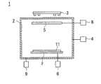
图1是对本发明中使用的成膜装置的一个例子进行说明的截面图。FIG. 1 is a cross-sectional view illustrating an example of a film forming apparatus used in the present invention.
图2中的(a)~(d)是用于说明半导体装置的制造工序的前半部分的截面图。(a)-(d) in FIG. 2 are sectional views for explaining the first half of the manufacturing process of the semiconductor device.
图3中的(a)、(b)是用于说明半导体装置的制造工序的后半部分的截面图。(a) and (b) in FIG. 3 are sectional views for explaining the second half of the manufacturing process of the semiconductor device.
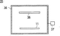
图4是用于说明加热装置的截面图。Fig. 4 is a cross-sectional view for explaining the heating device.
图5是半导体装置的立体图。5 is a perspective view of a semiconductor device.
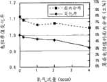
图6是表示氧流量与电阻率值变化率、薄层电阻(sheet resistance)值的面内分布的关系的图表。Fig. 6 is a graph showing the relationship between the oxygen flow rate, the rate of change of the resistivity value, and the in-plane distribution of the sheet resistance value.
附图标记的说明Explanation of reference signs
10半导体装置10 Semiconductor device
11处理对象物11Processing objects
14第一金属布线14 first metal wiring
21孔21 holes
22沟22 ditch
25中间层25 middle layer
26第一绝缘膜26 first insulating film
27第二绝缘膜27 second insulating film
28基底层28 basal layer
29阻挡膜29 barrier film
32第二金属布线32 second metal wiring
具体实施方式Detailed ways
图2(a)的附图标记11表示本发明中使用的处理对象物。处理对象物11具有衬底12,在衬底12的表面上形成有沟,在该沟内配置有第一金属布线14。
在衬底12的配置有第一金属布线14的表面上配置有下部绝缘层15,在下部绝缘层15的表面上配置有第一保护膜16,以下部绝缘层15和第一保护膜16构成第一绝缘膜26。The lower
在第一保护膜16的表面上配置有上部绝缘层17,在上部绝缘层17的表面上配置有第二保护膜18,以上部绝缘层17和第二保护膜18构成第二绝缘膜27。Upper insulating
在第一、第二绝缘膜26、27中在第一金属布线14的正上方的位置形成有贯通第一、第二绝缘膜26、27的贯通孔,第二绝缘膜27被构图,形成有通过与该贯通孔交叉的位置的沟22。In the first and second insulating
图2(a)的附图标记21表示作为贯通孔的贯通第一绝缘膜26的部分的孔,如上所述,因为沟22与贯通孔交叉,所以孔21的开口露出于沟22的底面上。
第一保护膜16被用作形成沟22时的上部绝缘层17的蚀刻阻止层(etching stopper),因此,第一保护膜16露出在沟22底面的孔21以外的部分上。The first
接着,使用该处理对象物11对制造半导体装置的本发明的制造方法进行说明。Next, the manufacturing method of the present invention for manufacturing a semiconductor device using the
图1的附图标记1表示本发明中使用的成膜装置的一例。
该成膜装置1具有:真空槽2;以及分别配制在真空槽2内部的衬底夹具7和靶5。This
在真空槽2上连接有真空排气系统9和气体供给系统4,对真空槽2内部进行真空排气,在进行真空排气的同时从气体供给系统4导入溅射气体和在化学结构中含氮或氧的反应气体(例如,在反应气体为氧气的情况下,流量为0.1sccm以上5sccm以下),在真空槽2内部形成比大气压低的成膜气氛(例如全压力为10-4Pa以上10-1Pa以下)。A
在将形成有沟22的面朝向靶5的状态下使衬底夹具7保持上述的处理对象物11。The object to be processed 11 described above is held by the
在真空槽2的外部分别配置有溅射电源8和偏置电源6,靶5与溅射电源8连接,衬底夹具7与偏置电源6连接。A sputtering
在真空槽2的外部配置有磁场形成单元3,使真空槽2为接地电位,在维持真空槽2内部的成膜气氛的同时,当向靶5施加负电压时,靶5被磁控溅射。A magnetic
靶5为以铜为主成分且添加有规定量的锰(例如超过2原子%)的合金靶,当靶5被磁控溅射时,释放出由以铜为主成分且添加有锰的合金材料构成的溅射粒子。The
释放出的溅射粒子和反应气体射入处理对象物11的形成有沟22的面,在该表面上生长在上述合金材料中含有反应气体的薄膜。The released sputtering particles and reactive gas are injected into the surface of the
此时,在衬底夹具7上施加有高频电压(包括0V),向处理对象物11的形成有沟22的面上射入与高频电压的大小相应的量的等离子体,对在表面上的生长薄膜进行蚀刻。At this time, a high-frequency voltage (including 0V) is applied to the
负电压和高频电压的大小被设定为,使得假定薄膜不被蚀刻时的薄膜的膜厚生长速度(溅射速度)大于假定薄膜不生长而仅被蚀刻时的膜厚减少速度(蚀刻速度),如图2(b)所示,薄膜25在沟22的侧壁和底面上、孔21的侧壁和底面上、以及第二绝缘膜27的表面上生长(中间层形成工序)。The magnitudes of the negative voltage and the high-frequency voltage are set so that the film thickness growth rate (sputtering rate) of the film assuming that the film is not etched is greater than the rate of decrease in film thickness (etching rate) of the film assuming that the film is only etched without growing. ), as shown in FIG. 2(b), the
将向靶5的负电压的施加和向衬底夹具7的高频电压的施加持续规定时间,在薄膜25生长至规定膜厚时候,在持续进行溅射气体和反应气体的导入和真空排气的同时,以使得薄膜的蚀刻速度变大的方式调整施加在靶5和衬底夹具7上的电压。例如,使施加在靶5上的电压比薄膜生长到规定膜厚之前小,减少溅射粒子的释放量并使溅射速度下降。此外,也可以使施加在衬底夹具7上的电压比薄膜生长到规定膜厚之前大,增加等离子体入射量并使蚀刻速度增加。The application of the negative voltage to the
因为等离子体大致垂直地射入孔21的底面,所以孔21的底面上的薄膜25被蚀刻,但是因为等离子体不垂直地射入孔21的侧壁和沟22的侧壁,所以薄膜25残留。Because the plasma is injected into the bottom surface of the
此时,施加在衬底夹具7上的高频电压、施加在靶5上的负电压和溅射气体的流量以在沟22的底面、和第二绝缘膜27的表面上残留薄膜25的方式设定,使高频电压的施加和负电压的施加持续规定时间,在中间层25从孔21的底面被除去并露出第一金属布线14时分别停止高频电压和负电压的施加(蚀刻工序)。At this time, the high-frequency voltage applied to the
图2(c)表示蚀刻工序结束后的状态,虽然第一金属布线14的表面露出在孔21的底面上,但中间层25残留在孔21的侧壁、沟22的底面和侧壁、以及第二绝缘膜27的表面上。Fig. 2 (c) shows the state after etching process finishes, although the surface of the
孔21的侧壁、沟22的底面和侧壁、以及第二绝缘膜27的表面上的中间层25连续。虽然中间层25被从孔21的底面除去,但是孔21的侧壁上的中间层25在孔21的底面上与第一金属布线14的表面接触,如上所述,因为中间层25以铜为主成分,所以孔21的侧壁上的中间层25、沟22的底面和侧壁的中间层25、以及第二绝缘膜27的表面上的中间层25与各第一金属布线14电连接。The sidewall of the
将此状态的处理对象物11浸渍在电解电镀液中,当向中间层25通电时,金属层31在位于第一金属布线14表面的孔21的底面的部分、和中间层25的表面上生长,沟22的内部和孔21的内部被金属层填充。图2(d)表示形成有金属层31的状态下的处理对象物11。The
图4的附图标记35表示加热装置,加热装置35具有加热室36和与加热室36连接的真空排气系统37。启动真空排气系统37,在加热室36的内部形成真空气氛,在维持该真空气氛的状态下,将形成有金属层31的处理对象物11搬入加热室36。
在加热室36的内部配置有加热器38,向该加热器38通电,为了防止金属层31的氧化,在维持真空气氛的同时,以比上述中间层形成工序和蚀刻工序时升温的温度更高的温度(例如在350℃下进行2小时)对该处理对象物11进行加热,对金属层31进行退火处理。A
锰在铜中的扩散速度较快,在进行退火处理时,当中间层25升温时,包含在中间层25中的锰扩散,分别到达孔21的侧壁、沟22的侧壁和底面、以及第二绝缘膜27的表面。The diffusion rate of manganese in copper is fast, and when the annealing treatment is carried out, when the temperature of the
下部绝缘层15和第一保护膜16位于孔21的侧壁,上部绝缘层17和第二保护膜18位于沟22的侧壁,这里,第一、第二保护膜16、18由SiN这样的氮化物构成,下部绝缘层15和上部绝缘层17由SiO2这样的氧化物构成。The lower insulating
锰对于氮和氧的反应性比铜高,而且,通过在中间层25中添加上述的反应气体,使得反应性变得更高。Manganese has higher reactivity with respect to nitrogen and oxygen than copper, and by adding the above-mentioned reactive gas to the
锰在第一保护膜16与中间层25的界面、以及第二保护膜18与中间层25的界面与包含在第一、第二保护膜16、18中的氮化物反应并析出氮化锰,并在下部绝缘层15与中间层25的界面、以及上部绝缘层17与中间层25的界面与包含在下部绝缘层15和上部绝缘层17中的氧化物反应并析出氧化锰。Manganese reacts with the nitride contained in the first and second
这时,在反应气体包含氮的情况下,在各界面析出作为反应气体的氮与锰的反应物的氮化锰;在反应气体包含氧的情况下,在各界面析出作为反应气体的氧与锰的反应物的氧化锰。At this time, when the reaction gas contains nitrogen, manganese nitride as a reactant of nitrogen and manganese in the reaction gas is precipitated at each interface; manganese reactant manganese oxide.
因此,在第一保护膜16与中间层25的界面、以及第二保护膜18与中间层25的界面,析出氮化锰、或氮化锰与氧化锰双方并形成阻挡膜29;在下部绝缘层15与中间层25的界面、以及上部绝缘层17与中间层25的界面,析出氧化锰、或氧化锰与氮化锰双方并形成阻挡膜29(图3(a))。Therefore, at the interface between the first
在阻挡膜29被形成时,作为中间层25的主成分的铜、Mn和反应气体的一部分残留在阻挡膜29的表面上,该残留的中间层25成为基底层28。When the
基底层28与中间层25同样地以铜为主成分,虽然铜容易扩散至氧化硅和硅中,但是因为氧化锰和氮化锰具有遮蔽铜的扩散的性质,所以铜被阻挡膜29遮蔽,既不会侵入下部绝缘层15,也不会侵入上部绝缘层17。Like the
接着,通过例如CMP(Chemical Mechanical Polishing:化学机械研磨)法对处理对象物11的形成有金属层31的面进行研磨,研磨除去金属层31直至露出第二绝缘层27的表面,于是沟22与沟22之间的金属层31被除去,填充在各沟22中的金属层31被相互分离,第二金属布线32被形成(图3(b))。Next, the surface on which the
图3(b)、图5的附图标记10表示形成有第二金属布线32的半导体装置。孔21的内部保持填充有金属层31的状态,以填充有金属层31的孔21构成相互连接第一、第二金属布线14、32的接触孔33。
如上所述,因为在孔21的底面上没有形成中间层25,所以在接触孔33与第一金属布线14之间未形成阻挡层,第一、第二金属布线14、32之间的电阻较低。As described above, since the
包含氧化锰和氮化锰中任一方或两方的阻挡膜29,对SiO2、SiN等硅化合物,以及铜、铝等金属材料这两方的粘接性较高。The
因为阻挡膜29位于以铜为主成分的基底层28与含有SiO2、SiN的第一、第二绝缘膜26、27之间,所以基底层28被牢固地固定在沟22的底面和侧壁、以及孔21的内壁上。因为基底层28与第二金属布线32的贴紧性较高,且第二金属布线32通过基底层28和阻挡膜29被固定在沟22内,所以难以从半导体装置10脱落。Because the
以上,对在中间层形成工序之后进行蚀刻工序,使金属布线14露出在孔21的底面上的情况进行了说明,但本发明并不限定于此,只要第一、第二金属布线14、32之间的电阻降低为能够容许的程度,中间层25也可以残留在孔21的底面上。In the above, the case where the etching step is performed after the intermediate layer forming step to expose the
以上,对令基底层为一层结构的情况进行了说明,但本发明并不限定于此。例如,也可以在真空槽2的内部除了配置合金靶5之外,另外配置高纯度的铜靶,在蚀刻工序结束之后,对高纯度铜靶进行溅射,层叠铜薄膜,层叠2层以上的基底层。In the above, the case where the base layer has a one-layer structure has been described, but the present invention is not limited thereto. For example, in addition to disposing the
在此情况下,在蚀刻工序中,即使中间层25被从沟22的底面除去,中间层25被分裂,因为被分裂的中间层25通过生长在沟22的底面上的铜薄膜被电连接,所以能够通过电镀法形成填充沟22的金属层31。但是,当SiO2的膜露出在沟22的底面上时,因为铜从铜薄膜扩散,所以在此情况下,优选具有铜的遮蔽性的膜(例如SiN膜)位于第一绝缘膜26的表面上。In this case, in the etching process, even if the
第一保护膜16的构成材料与上部绝缘层17相比,蚀刻速度较慢,在对上部绝缘层17进行构图时,如果能够作为蚀刻阻止层发挥作用,则不限定于SiN。The constituent material of the first
加热中间层25形成阻挡膜和基底层的加热工序也可以在形成金属层31之前进行,但是如果在形成金属层31之后进行,则中间层25的加热和金属层31的退火化被同时进行,不仅能够缩短制造时间,还能够不对处理对象物11施加多余的热损伤。The heating step of heating the
此外,在对合金靶进行溅射时,在被加热的温度下如果扩散性金属的氮化物或氧化物在处理对象物11与中间层25的界面析出,则没有必要特别设置对中间层25进行加热的工序。In addition, when the alloy target is sputtered, if the nitride or oxide of the diffusible metal is precipitated at the interface between the
以上,对使用添加有作为扩散性金属的Mn的合金靶(靶5)的情况进行了说明,但本发明不限定于此。As mentioned above, although the case where the alloy target (target 5) to which Mn was added as a diffusible metal was used was demonstrated, this invention is not limited to this.
扩散性金属只要是在铜中的扩散速度快,且与氮或氧反应的金属的话,除了Mn以外,还能够使用Ti、Ta、Mo、W、V等各种过渡金属,以及Mg、Al等非过渡金属作为扩散性金属添加在靶5中。As long as the diffusible metal has a fast diffusion rate in copper and reacts with nitrogen or oxygen, in addition to Mn, various transition metals such as Ti, Ta, Mo, W, V, and Mg, Al, etc. can be used. A non-transition metal is added to the
这些过渡金属既可以单独地添加在合金靶5中,也可以添加2种以上。These transition metals may be added to the
合金靶5中的扩散性金属的添加量虽然没有特别限定,但是其添加量例如为1原子%以上40原子%以下。The addition amount of the diffusible metal in the
反应气体只要是在化学结构中包含氧或氮,且与扩散性金属反应生成氧化物或氮化物的气体的话,没有特别限定,例如能够使用H2O、O3、CO、N2、NH3。这些反应气体既可以单独使用一种,也可以使用2种以上。The reaction gas is not particularly limited as long as it contains oxygen or nitrogen in its chemical structure and reacts with diffusible metals to form oxides or nitrides. For example, H2 O, O3 , CO, N2 , NH3 can be used. . These reaction gases may be used alone or in combination of two or more.
溅射气体没有特别限定,能够使用从包括Ar气体、Ne气体、Xe气体、和Kr气体的组中选择的惰性气体中的至少一种。The sputtering gas is not particularly limited, and at least one of inert gases selected from the group consisting of Ar gas, Ne gas, Xe gas, and Kr gas can be used.
下部绝缘层15和上部绝缘层17的构成材料并不限定于由SiO2构成的情况,能够使用含有从包括SiO2、SiN、SiOC、和SiC构成的组中选择的至少一种以上的材料。The constituent materials of lower insulating
第一、第二金属布线14、32的构成材料没有特别限定,能够使用Cu、Al等各种导电性材料,但是因为基底层28以铜为主成分,所以考虑与基底层28的贴紧性,优选第二金属布线32的构成材料是以铜为主成分的材料,在第二金属布线32的构成材料以铜为主成分的情况下,考虑电气特性,优选第一金属布线14的构成材料是以铜为主成分的材料。The constituent materials of the first and
以上,对在第一绝缘膜26之上配置有第二绝缘膜27,且孔21位于第二绝缘膜27的沟22底面的处理对象物11进行了说明,但本发明并不限定于此。The
例如,使用未形成有第二绝缘膜27、且第一绝缘膜26的表面露出的处理对象物11,制造半导体装置的情况也包括在本发明中。For example, the case of manufacturing a semiconductor device using the
在进行中间层形成工序和蚀刻工序时导入到真空槽2的反应气体的流量虽然没有特别限定,但是例如为0.1sccm以上5sccm以下,这时的真空槽2内部的压力例如为10-4Pa以上10-1Pa以下。The flow rate of the reaction gas introduced into the
以上,对在中间层形成工序和蚀刻工序中使靶5的施加电压两阶段地减少的情况进行了说明,但本发明并不限定于此,既可以3次以上分阶段地使靶5的施加电压减少,也可以不是阶段地而是连续地使靶5的施加电压逐渐减少。同样地,既可以3次以上分阶段地使高频电压增加,也可以不是阶段地而是连续地使高频电压逐渐增加。Above, the case where the voltage applied to the
实施例Example
(贴紧性试验)(adhesion test)
分别改变成膜气氛中的反应气体(O2、氧)的分压、和靶5的Mn添加量,进行中间层形成工序和蚀刻工序,形成中间层25,之后,以上述的工序制造成半导体装置10。这里,退火化的条件为:真空气氛的压力为6×10⁻⁶Pa,加热温度为350℃,加热时间为1小时。The partial pressure of the reaction gas (O2 , oxygen) in the film-forming atmosphere and the amount of Mn added to the
在获得的半导体装置10的形成有第二金属布线32一侧的表面上,形成了栅状的损伤。在半导体元件10表面的形成有损伤的部分粘贴粘接带后将其剥离,观察第二金属布线32有无剥离。将其结果与氧分压和靶5的Mn添加量一起记载在下述表1中。On the surface of the obtained
(表1)(Table 1)
表1:贴紧性试验Table 1: Adhesion test
上述表1的“○”是未观察到第二金属布线32的剥离的情况,“×”表示观察到第二金属布线32的剥离的情况。"◯" in Table 1 above indicates a case where no peeling of the
从上述表1明显可知,当Mn的添加量为2原子%以下,且氧气的分压不到10-3Pa时,贴紧性较差。从该实验结果能够确认到,如果Mn的添加量超过2原子%,且氧气的分压为10-3Pa以上,则第二金属布线32的贴紧性变高。It is clear from the above Table 1 that when the amount of Mn added is 2 atomic % or less and the partial pressure of oxygen is less than 10-3 Pa, the adhesiveness is poor. From the experimental results, it can be confirmed that when the addition amount of Mn exceeds 2 atomic % and the partial pressure of oxygen is 10−3 Pa or higher, the adhesiveness of the
(电阻值)(resistance)
使用Mn添加量为7原子%的靶,分别改变作为反应气体的氧气的流量,进行中间层形成工序和蚀刻工序,在形成中间层25之后,以上述的工序制造成半导体装置10。Using a target with an added amount of Mn of 7 atomic %, the flow rate of oxygen as a reaction gas was varied, and the intermediate layer forming step and etching step were performed. After the
对各半导体装置10的第一、第二金属布线14、32的电阻率和电阻值变化进行测定,其测定结果表示在图6的图表中。The resistivity and resistance value change of the first and
从图6明显可知,即使增加氧气流量,也没有发现引起第一、第二金属布线14、32的布线电阻值增加这样的电阻率的上升。由此可知,即使在中间层形成工序和蚀刻工序中导入氧气,金属布线的电气特性也不会劣化。As is apparent from FIG. 6 , even when the flow rate of oxygen gas was increased, no increase in resistivity that would cause an increase in the wiring resistance values of the first and
Claims (5)
Applications Claiming Priority (3)
| Application Number | Priority Date | Filing Date | Title |
|---|---|---|---|
| JP193879/2006 | 2006-07-14 | ||
| JP2006193879 | 2006-07-14 | ||
| PCT/JP2007/063891WO2008007732A1 (en) | 2006-07-14 | 2007-07-12 | Method for manufacturing semiconductor device |
Publications (2)
| Publication Number | Publication Date |
|---|---|
| CN101490811A CN101490811A (en) | 2009-07-22 |
| CN101490811Btrue CN101490811B (en) | 2011-06-08 |
Family
ID=38923288
Family Applications (1)
| Application Number | Title | Priority Date | Filing Date |
|---|---|---|---|
| CN2007800266022AExpired - Fee RelatedCN101490811B (en) | 2006-07-14 | 2007-07-12 | Method for manufacturing semiconductor device |
Country Status (6)
| Country | Link |
|---|---|
| US (1) | US20090120787A1 (en) |
| JP (1) | JP5145225B2 (en) |
| KR (1) | KR101059709B1 (en) |
| CN (1) | CN101490811B (en) |
| TW (1) | TWI397125B (en) |
| WO (1) | WO2008007732A1 (en) |
Families Citing this family (10)
| Publication number | Priority date | Publication date | Assignee | Title |
|---|---|---|---|---|
| JP5820267B2 (en)* | 2008-03-21 | 2015-11-24 | プレジデント アンド フェローズ オブ ハーバード カレッジ | Self-aligned barrier layer for wiring |
| JP5343417B2 (en)* | 2008-06-25 | 2013-11-13 | 富士通セミコンダクター株式会社 | Semiconductor device and manufacturing method thereof |
| JP5339830B2 (en)* | 2008-09-22 | 2013-11-13 | 三菱マテリアル株式会社 | Thin film transistor wiring film having excellent adhesion and sputtering target for forming this wiring film |
| JP5466889B2 (en)* | 2009-06-18 | 2014-04-09 | 東京エレクトロン株式会社 | Method for forming multilayer wiring |
| JP2013080779A (en)* | 2011-10-03 | 2013-05-02 | Ulvac Japan Ltd | Semiconductor device manufacturing method and semiconductor device |
| US9048294B2 (en)* | 2012-04-13 | 2015-06-02 | Applied Materials, Inc. | Methods for depositing manganese and manganese nitrides |
| US9076661B2 (en) | 2012-04-13 | 2015-07-07 | Applied Materials, Inc. | Methods for manganese nitride integration |
| KR20150031239A (en)* | 2012-06-18 | 2015-03-23 | 도쿄엘렉트론가부시키가이샤 | Method for forming film containing manganese |
| TWI609095B (en)* | 2013-05-30 | 2017-12-21 | 應用材料股份有限公司 | Methods for manganese nitride integration |
| US9275952B2 (en)* | 2014-01-24 | 2016-03-01 | International Business Machines Corporation | Ultrathin superlattice of MnO/Mn/MnN and other metal oxide/metal/metal nitride liners and caps for copper low dielectric constant interconnects |
Citations (3)
| Publication number | Priority date | Publication date | Assignee | Title |
|---|---|---|---|---|
| US6037257A (en)* | 1997-05-08 | 2000-03-14 | Applied Materials, Inc. | Sputter deposition and annealing of copper alloy metallization |
| EP1029943B1 (en)* | 1999-02-17 | 2005-04-27 | Nihon Shinku Gijutsu Kabushiki Kaisha | Process for producing barrier film |
| CN1643683A (en)* | 2002-01-24 | 2005-07-20 | 霍尼韦尔国际公司 | Thin films, structures having thin films, and methods of forming thin films |
Family Cites Families (10)
| Publication number | Priority date | Publication date | Assignee | Title |
|---|---|---|---|---|
| US4579618A (en)* | 1984-01-06 | 1986-04-01 | Tegal Corporation | Plasma reactor apparatus |
| JPH06333925A (en)* | 1993-05-20 | 1994-12-02 | Nippon Steel Corp | Semiconductor integrated circuit and manufacturing method thereof |
| US6387805B2 (en)* | 1997-05-08 | 2002-05-14 | Applied Materials, Inc. | Copper alloy seed layer for copper metallization |
| JP4360716B2 (en)* | 1999-09-02 | 2009-11-11 | 株式会社アルバック | Copper thin film manufacturing method and sputtering apparatus used in the method |
| US6491835B1 (en)* | 1999-12-20 | 2002-12-10 | Applied Materials, Inc. | Metal mask etching of silicon |
| US6764940B1 (en)* | 2001-03-13 | 2004-07-20 | Novellus Systems, Inc. | Method for depositing a diffusion barrier for copper interconnect applications |
| JP3944437B2 (en) | 2001-10-05 | 2007-07-11 | 株式会社半導体理工学研究センター | Electroless plating method, method for forming embedded wiring, and embedded wiring |
| JP2005166757A (en)* | 2003-11-28 | 2005-06-23 | Advanced Lcd Technologies Development Center Co Ltd | Wiring structure, wiring structure forming method, thin film transistor, thin film transistor forming method, and display device |
| JP4478038B2 (en) | 2004-02-27 | 2010-06-09 | 株式会社半導体理工学研究センター | Semiconductor device and manufacturing method thereof |
| JP2005285820A (en)* | 2004-03-26 | 2005-10-13 | Ulvac Japan Ltd | Bias spatter film deposition process and film thickness control method |
- 2007
- 2007-07-12KRKR1020087029414Apatent/KR101059709B1/ennot_activeExpired - Fee Related
- 2007-07-12WOPCT/JP2007/063891patent/WO2008007732A1/enactiveApplication Filing
- 2007-07-12JPJP2008524834Apatent/JP5145225B2/ennot_activeExpired - Fee Related
- 2007-07-12CNCN2007800266022Apatent/CN101490811B/ennot_activeExpired - Fee Related
- 2007-07-13TWTW096125743Apatent/TWI397125B/enactive
- 2009
- 2009-01-12USUS12/352,011patent/US20090120787A1/ennot_activeAbandoned
Patent Citations (3)
| Publication number | Priority date | Publication date | Assignee | Title |
|---|---|---|---|---|
| US6037257A (en)* | 1997-05-08 | 2000-03-14 | Applied Materials, Inc. | Sputter deposition and annealing of copper alloy metallization |
| EP1029943B1 (en)* | 1999-02-17 | 2005-04-27 | Nihon Shinku Gijutsu Kabushiki Kaisha | Process for producing barrier film |
| CN1643683A (en)* | 2002-01-24 | 2005-07-20 | 霍尼韦尔国际公司 | Thin films, structures having thin films, and methods of forming thin films |
Non-Patent Citations (3)
| Title |
|---|
| JP特开2003-178999A 2003.06.27 |
| JP特开2005-166757A 2005.06.23 |
| JP特开2005-277390A 2005.10.06 |
Also Published As
| Publication number | Publication date |
|---|---|
| KR20090010089A (en) | 2009-01-28 |
| WO2008007732A1 (en) | 2008-01-17 |
| CN101490811A (en) | 2009-07-22 |
| TW200811954A (en) | 2008-03-01 |
| KR101059709B1 (en) | 2011-08-29 |
| JP5145225B2 (en) | 2013-02-13 |
| JPWO2008007732A1 (en) | 2009-12-10 |
| US20090120787A1 (en) | 2009-05-14 |
| TWI397125B (en) | 2013-05-21 |
Similar Documents
| Publication | Publication Date | Title |
|---|---|---|
| CN101490811B (en) | Method for manufacturing semiconductor device | |
| CN101715602B (en) | Film forming method and film forming apparatus | |
| TWI383426B (en) | A method for forming a barrier film and a method for forming an electrode film | |
| CN101897016A (en) | Method for manufacturing semiconductor device, electronic apparatus, semiconductor manufacturing apparatus, and storage medium | |
| TWI374482B (en) | ||
| WO2008044757A1 (en) | Conductive film forming method, thin film transistor, panel with thin film transistor and thin film transistor manufacturing method | |
| JPH03111571A (en) | Formation of deposited film | |
| TW202000967A (en) | Treatment and doping of barrier layers | |
| GB2319533A (en) | Methods of forming a barrier layer based on titanium nitride | |
| US20050003663A1 (en) | Integrated circuit having barrier metal surface treatment prior to Cu deposition | |
| JP2008124450A (en) | Target, film forming method, thin film transistor, panel with thin film transistor, manufacturing method for thin film transistor, and manufacturing method for panel with thin film transistor | |
| TWI528480B (en) | Mounting device, and method for manufacturing same | |
| CN100523293C (en) | Film forming method and film forming apparatus | |
| JP2010232538A (en) | Semiconductor device and manufacturing method thereof | |
| JP2008098522A (en) | Method and apparatus for manufacturing semiconductor device | |
| JP5424876B2 (en) | Thin film transistor manufacturing method, liquid crystal display device manufacturing method, and electrode forming method | |
| JPH07263359A (en) | Method of forming thin film | |
| JP5031953B2 (en) | Copper material filled plug and method for producing copper material filled plug | |
| JP3273827B2 (en) | Semiconductor device and manufacturing method thereof | |
| JP4959122B2 (en) | Method for forming vanadium-containing film | |
| CN101091001B (en) | Method for forming tantalum nitride film | |
| JP2006183145A (en) | Method of forming film, film forming apparatus and storage medium | |
| JP2006093551A (en) | Method of forming titanium content film | |
| JP2009044056A (en) | Method for manufacturing copper film | |
| TWI503926B (en) | Semiconductor device manufacturing method and semiconductor device |
Legal Events
| Date | Code | Title | Description |
|---|---|---|---|
| C06 | Publication | ||
| PB01 | Publication | ||
| C10 | Entry into substantive examination | ||
| SE01 | Entry into force of request for substantive examination | ||
| C14 | Grant of patent or utility model | ||
| GR01 | Patent grant | ||
| CF01 | Termination of patent right due to non-payment of annual fee | Granted publication date:20110608 | |
| CF01 | Termination of patent right due to non-payment of annual fee |