CN101490768B - Transparent conductive laminated body and touch panel comprising the laminated body - Google Patents
Transparent conductive laminated body and touch panel comprising the laminated bodyDownload PDFInfo
- Publication number
- CN101490768B CN101490768BCN2007800273948ACN200780027394ACN101490768BCN 101490768 BCN101490768 BCN 101490768BCN 2007800273948 ACN2007800273948 ACN 2007800273948ACN 200780027394 ACN200780027394 ACN 200780027394ACN 101490768 BCN101490768 BCN 101490768B
- Authority
- CN
- China
- Prior art keywords
- film
- transparent
- thickness
- thin film
- substrate
- Prior art date
- Legal status (The legal status is an assumption and is not a legal conclusion. Google has not performed a legal analysis and makes no representation as to the accuracy of the status listed.)
- Active
Links
Images


Classifications
- G—PHYSICS
- G06—COMPUTING OR CALCULATING; COUNTING
- G06F—ELECTRIC DIGITAL DATA PROCESSING
- G06F3/00—Input arrangements for transferring data to be processed into a form capable of being handled by the computer; Output arrangements for transferring data from processing unit to output unit, e.g. interface arrangements
- G06F3/01—Input arrangements or combined input and output arrangements for interaction between user and computer
- G06F3/03—Arrangements for converting the position or the displacement of a member into a coded form
- G06F3/041—Digitisers, e.g. for touch screens or touch pads, characterised by the transducing means
- G06F3/0414—Digitisers, e.g. for touch screens or touch pads, characterised by the transducing means using force sensing means to determine a position
- B—PERFORMING OPERATIONS; TRANSPORTING
- B32—LAYERED PRODUCTS
- B32B—LAYERED PRODUCTS, i.e. PRODUCTS BUILT-UP OF STRATA OF FLAT OR NON-FLAT, e.g. CELLULAR OR HONEYCOMB, FORM
- B32B5/00—Layered products characterised by the non- homogeneity or physical structure, i.e. comprising a fibrous, filamentary, particulate or foam layer; Layered products characterised by having a layer differing constitutionally or physically in different parts
- B32B5/16—Layered products characterised by the non- homogeneity or physical structure, i.e. comprising a fibrous, filamentary, particulate or foam layer; Layered products characterised by having a layer differing constitutionally or physically in different parts characterised by features of a layer formed of particles, e.g. chips, powder or granules
- B—PERFORMING OPERATIONS; TRANSPORTING
- B32—LAYERED PRODUCTS
- B32B—LAYERED PRODUCTS, i.e. PRODUCTS BUILT-UP OF STRATA OF FLAT OR NON-FLAT, e.g. CELLULAR OR HONEYCOMB, FORM
- B32B7/00—Layered products characterised by the relation between layers; Layered products characterised by the relative orientation of features between layers, or by the relative values of a measurable parameter between layers, i.e. products comprising layers having different physical, chemical or physicochemical properties; Layered products characterised by the interconnection of layers
- B32B7/02—Physical, chemical or physicochemical properties
- B32B7/023—Optical properties
- B—PERFORMING OPERATIONS; TRANSPORTING
- B32—LAYERED PRODUCTS
- B32B—LAYERED PRODUCTS, i.e. PRODUCTS BUILT-UP OF STRATA OF FLAT OR NON-FLAT, e.g. CELLULAR OR HONEYCOMB, FORM
- B32B7/00—Layered products characterised by the relation between layers; Layered products characterised by the relative orientation of features between layers, or by the relative values of a measurable parameter between layers, i.e. products comprising layers having different physical, chemical or physicochemical properties; Layered products characterised by the interconnection of layers
- B32B7/04—Interconnection of layers
- B32B7/12—Interconnection of layers using interposed adhesives or interposed materials with bonding properties
- G—PHYSICS
- G06—COMPUTING OR CALCULATING; COUNTING
- G06F—ELECTRIC DIGITAL DATA PROCESSING
- G06F3/00—Input arrangements for transferring data to be processed into a form capable of being handled by the computer; Output arrangements for transferring data from processing unit to output unit, e.g. interface arrangements
- G06F3/01—Input arrangements or combined input and output arrangements for interaction between user and computer
- G06F3/03—Arrangements for converting the position or the displacement of a member into a coded form
- G06F3/041—Digitisers, e.g. for touch screens or touch pads, characterised by the transducing means
- G06F3/045—Digitisers, e.g. for touch screens or touch pads, characterised by the transducing means using resistive elements, e.g. a single continuous surface or two parallel surfaces put in contact
- H—ELECTRICITY
- H01—ELECTRIC ELEMENTS
- H01B—CABLES; CONDUCTORS; INSULATORS; SELECTION OF MATERIALS FOR THEIR CONDUCTIVE, INSULATING OR DIELECTRIC PROPERTIES
- H01B5/00—Non-insulated conductors or conductive bodies characterised by their form
- H01B5/14—Non-insulated conductors or conductive bodies characterised by their form comprising conductive layers or films on insulating-supports
- B—PERFORMING OPERATIONS; TRANSPORTING
- B32—LAYERED PRODUCTS
- B32B—LAYERED PRODUCTS, i.e. PRODUCTS BUILT-UP OF STRATA OF FLAT OR NON-FLAT, e.g. CELLULAR OR HONEYCOMB, FORM
- B32B2264/00—Composition or properties of particles which form a particulate layer or are present as additives
- B32B2264/10—Inorganic particles
- B32B2264/102—Oxide or hydroxide
- B—PERFORMING OPERATIONS; TRANSPORTING
- B32—LAYERED PRODUCTS
- B32B—LAYERED PRODUCTS, i.e. PRODUCTS BUILT-UP OF STRATA OF FLAT OR NON-FLAT, e.g. CELLULAR OR HONEYCOMB, FORM
- B32B2307/00—Properties of the layers or laminate
- B32B2307/20—Properties of the layers or laminate having particular electrical or magnetic properties, e.g. piezoelectric
- B32B2307/202—Conductive
- B—PERFORMING OPERATIONS; TRANSPORTING
- B32—LAYERED PRODUCTS
- B32B—LAYERED PRODUCTS, i.e. PRODUCTS BUILT-UP OF STRATA OF FLAT OR NON-FLAT, e.g. CELLULAR OR HONEYCOMB, FORM
- B32B2307/00—Properties of the layers or laminate
- B32B2307/40—Properties of the layers or laminate having particular optical properties
- B32B2307/412—Transparent
- B—PERFORMING OPERATIONS; TRANSPORTING
- B32—LAYERED PRODUCTS
- B32B—LAYERED PRODUCTS, i.e. PRODUCTS BUILT-UP OF STRATA OF FLAT OR NON-FLAT, e.g. CELLULAR OR HONEYCOMB, FORM
- B32B2307/00—Properties of the layers or laminate
- B32B2307/50—Properties of the layers or laminate having particular mechanical properties
- B32B2307/536—Hardness
- Y—GENERAL TAGGING OF NEW TECHNOLOGICAL DEVELOPMENTS; GENERAL TAGGING OF CROSS-SECTIONAL TECHNOLOGIES SPANNING OVER SEVERAL SECTIONS OF THE IPC; TECHNICAL SUBJECTS COVERED BY FORMER USPC CROSS-REFERENCE ART COLLECTIONS [XRACs] AND DIGESTS
- Y10—TECHNICAL SUBJECTS COVERED BY FORMER USPC
- Y10T—TECHNICAL SUBJECTS COVERED BY FORMER US CLASSIFICATION
- Y10T428/00—Stock material or miscellaneous articles
- Y10T428/24—Structurally defined web or sheet [e.g., overall dimension, etc.]
- Y10T428/24942—Structurally defined web or sheet [e.g., overall dimension, etc.] including components having same physical characteristic in differing degree
- Y—GENERAL TAGGING OF NEW TECHNOLOGICAL DEVELOPMENTS; GENERAL TAGGING OF CROSS-SECTIONAL TECHNOLOGIES SPANNING OVER SEVERAL SECTIONS OF THE IPC; TECHNICAL SUBJECTS COVERED BY FORMER USPC CROSS-REFERENCE ART COLLECTIONS [XRACs] AND DIGESTS
- Y10—TECHNICAL SUBJECTS COVERED BY FORMER USPC
- Y10T—TECHNICAL SUBJECTS COVERED BY FORMER US CLASSIFICATION
- Y10T428/00—Stock material or miscellaneous articles
- Y10T428/25—Web or sheet containing structurally defined element or component and including a second component containing structurally defined particles
- Y10T428/256—Heavy metal or aluminum or compound thereof
- Y—GENERAL TAGGING OF NEW TECHNOLOGICAL DEVELOPMENTS; GENERAL TAGGING OF CROSS-SECTIONAL TECHNOLOGIES SPANNING OVER SEVERAL SECTIONS OF THE IPC; TECHNICAL SUBJECTS COVERED BY FORMER USPC CROSS-REFERENCE ART COLLECTIONS [XRACs] AND DIGESTS
- Y10—TECHNICAL SUBJECTS COVERED BY FORMER USPC
- Y10T—TECHNICAL SUBJECTS COVERED BY FORMER US CLASSIFICATION
- Y10T428/00—Stock material or miscellaneous articles
- Y10T428/26—Web or sheet containing structurally defined element or component, the element or component having a specified physical dimension
- Y10T428/263—Coating layer not in excess of 5 mils thick or equivalent
- Y10T428/264—Up to 3 mils
- Y10T428/265—1 mil or less
- Y—GENERAL TAGGING OF NEW TECHNOLOGICAL DEVELOPMENTS; GENERAL TAGGING OF CROSS-SECTIONAL TECHNOLOGIES SPANNING OVER SEVERAL SECTIONS OF THE IPC; TECHNICAL SUBJECTS COVERED BY FORMER USPC CROSS-REFERENCE ART COLLECTIONS [XRACs] AND DIGESTS
- Y10—TECHNICAL SUBJECTS COVERED BY FORMER USPC
- Y10T—TECHNICAL SUBJECTS COVERED BY FORMER US CLASSIFICATION
- Y10T428/00—Stock material or miscellaneous articles
- Y10T428/26—Web or sheet containing structurally defined element or component, the element or component having a specified physical dimension
- Y10T428/269—Web or sheet containing structurally defined element or component, the element or component having a specified physical dimension including synthetic resin or polymer layer or component
Landscapes
- Engineering & Computer Science (AREA)
- General Engineering & Computer Science (AREA)
- Theoretical Computer Science (AREA)
- Human Computer Interaction (AREA)
- Physics & Mathematics (AREA)
- General Physics & Mathematics (AREA)
- Life Sciences & Earth Sciences (AREA)
- Wood Science & Technology (AREA)
- Laminated Bodies (AREA)
- Non-Insulated Conductors (AREA)
- Position Input By Displaying (AREA)
Abstract
Translated fromChinese
Description
Translated fromChinese技术领域technical field
本发明涉及一种在可见光线区域具有透明性而且在薄膜基材上具备导电性薄膜的透明导电性层叠体及具备该层叠体的触摸面板。本发明的透明导电性层叠体除了可以用于液晶显示器、电致发光显示器等显示器方式或触摸面板等中的透明电极以外,还可以用于防止透明物品受到静电干扰或隔绝电磁波等。The present invention relates to a transparent conductive laminate having transparency in the visible light region and having a conductive film on a film substrate, and a touch panel including the laminate. The transparent conductive laminate of the present invention can be used for transparent electrodes in display systems such as liquid crystal displays and electroluminescent displays, touch panels, etc., and can be used to prevent electrostatic interference of transparent articles, block electromagnetic waves, and the like.
背景技术Background technique
在触摸面板中,根据位置检测的方法不同,有光学方式、超声波方式、静电电容方式、电阻膜方式等。其中,电阻膜方式由于其构造简单,因此在性价比方面出色,近年来正快速普及。电阻膜方式触摸面板被用于例如银行的现金自动存款、提款机(ATM)或交通机构的售票机等的显示板中。In the touch panel, depending on the method of position detection, there are an optical method, an ultrasonic method, an electrostatic capacitance method, a resistive film method, and the like. Among them, the resistive film method is excellent in terms of cost performance due to its simple structure, and has been rapidly popularized in recent years. The resistive touch panel is used, for example, in a display panel of an automatic deposit machine of a bank, a teller machine (ATM), or a ticket vending machine of a transportation institution.
该电阻膜方式的触摸面板经由隔离件地将透明导电性层叠体和带有透明导电性薄膜的玻璃对置,形成在透明导电性层叠体中流过电流而计测带有透明导电性薄膜的玻璃中的电压的这样的构造。如果通过利用手指或笔等的按压操作使透明导电性层叠体与带有透明导电性薄膜的玻璃接触,则可以通过该接触部分通电,来探知该接触部分的位置。In this resistive film type touch panel, a transparent conductive laminate and a glass with a transparent conductive film are opposed to each other through a spacer, and a current is passed through the transparent conductive laminate to measure the glass with a transparent conductive film. in such a configuration of the voltage. When the transparent conductive laminate is brought into contact with the glass with the transparent conductive film by pressing with a finger or a pen, the position of the contact portion can be detected by energizing the contact portion.
然而,近年来搭载于智能手机(smart phone)或PDA(Personal DigitalAssistance)、游戏机等中的触摸面板的市场正在增长,触摸面板的窄边框化不断推进。这样,用手指按压触摸面板的机会变多,除了笔输入耐久性以外,对于表面压力耐久性方面也需要满足。However, in recent years, the market for touch panels installed in smartphones (smartphones), PDAs (Personal Digital Assistance), game consoles, etc. is growing, and the narrower frame of touch panels is advancing. In this way, there are many opportunities to press the touch panel with fingers, and it is necessary to satisfy not only durability of pen input but also durability of surface pressure.
作为上述触摸面板,公开了例如在透明薄膜基材的至少一面上具备设有由至少包括平均粒径为1~30nm的微粒的树脂形成的、具有Ra为4~20nm的中心线平均粗糙度的结合层、SiOx层、透明导电层的透明导电性薄膜的触摸面板(参照下述专利文献1)。但是,为此构成时,透明导电层的表面电阻值发生变化,存在缺乏可靠性的问题。As the above-mentioned touch panel, there is disclosed, for example, that on at least one side of a transparent film substrate, a resin having at least particles having an average particle diameter of 1 to 30 nm is provided, and has a centerline average roughness of Ra of 4 to 20 nm. A touch panel of a transparent conductive thin film comprising an adhesive layer, aSiOx layer, and a transparent conductive layer (see
另外,作为上述触摸面板,公开了例如具备依次层叠了基材、用于固定导电层的结合层、导电层的透明导电性薄膜的触摸面板(参照下述专利文献2)。根据该专利文献2,还记载着结合层是利用等离子体CVD法形成的二氧化硅层。但是,在专利文献2记载的发明中,虽然记载着对附加笔输入触摸面板等大的滑动也能充分耐受的旨意,但表面压力耐久性并不充分。In addition, as the above-mentioned touch panel, for example, a touch panel including a transparent conductive film in which a substrate, an adhesive layer for fixing a conductive layer, and a conductive layer are sequentially laminated is disclosed (see
专利文献1 日本特开2002-117724号公报
专利文献2 日本特开2003-320609号公报
发明内容Contents of the invention
本发明鉴于上述问题点而设,目的在于提供一种表面压力耐久性出色的透明导电性层叠体及具备该层叠体的触摸面板。The present invention was made in view of the above problems, and an object of the present invention is to provide a transparent conductive laminate excellent in surface pressure durability and a touch panel including the laminate.
本发明人等为了解决上述现有问题,对透明导电性层叠体及具备该层叠体的触摸面板进行了深入研究。结果发现,通过采用下述构成可以实现上述目的,从而完成了本发明。In order to solve the above conventional problems, the inventors of the present invention conducted intensive studies on a transparent conductive laminate and a touch panel including the laminate. As a result, the inventors have found that the above object can be achieved by employing the following configurations, and have completed the present invention.
即,本发明涉及一种透明导电性层叠体,其是在透明的薄膜基材的一个面经由电介质薄膜设有透明的导电性薄膜,在透明的薄膜基材的另一个面,经由透明的粘合剂层贴合有透明基体的透明导电性层叠体,其特征是,That is, the present invention relates to a transparent conductive laminate in which a transparent conductive film is provided on one side of a transparent film base via a dielectric film, and the other side of the transparent film base is provided via a transparent adhesive. A transparent conductive laminate having a transparent substrate bonded to the mixture layer is characterized in that,
上述透明基体是将至少2张透明的基体薄膜经由透明的粘合剂层而层叠的层叠透明基体;The above-mentioned transparent substrate is a laminated transparent substrate in which at least two transparent substrate films are laminated via a transparent adhesive layer;
上述电介质薄膜由第一透明电介质薄膜和第二透明电介质薄膜形成,所述第一透明电介质薄膜由相对折射率为1.6~1.9的SiOx膜(x为1.5以上且小于2)制成,所述第二透明电介质薄膜由SiO2膜制成。The above-mentioned dielectric thin film is formed by a first transparent dielectric thin film and a second transparent dielectric thin film, the first transparent dielectric thin film is made of a SiOx film (x is more than 1.5 and less than 2) with a relative refractive index of 1.6 to 1.9, and the The second transparent dielectric film is made ofSiO2 film.
在上述透明导电性层叠体中,上述电介质薄膜中,优选从薄膜基材的一侧开始依次形成有第一透明电介质薄膜及第二透明电介质薄膜。In the above-mentioned transparent conductive laminate, it is preferable that the first transparent dielectric thin film and the second transparent dielectric thin film are formed in order from the side of the film substrate in the dielectric thin film.
在上述透明导电性层叠体中,上述第一透明电介质薄膜优选为利用干式程序而设置的薄膜。In the above transparent conductive laminate, it is preferable that the first transparent dielectric thin film is formed by a dry process.
在上述透明导电性层叠体中,优选上述第一透明电介质薄膜的厚度为1nm~30nm、上述第二透明电介质薄膜的厚度为10nm~70nm、上述透明导电性薄膜的厚度为20nm~35nm。In the transparent conductive laminate, it is preferable that the first transparent dielectric film has a thickness of 1 nm to 30 nm, the second transparent dielectric film has a thickness of 10 nm to 70 nm, and the transparent conductive film has a thickness of 20 nm to 35 nm.
在上述透明导电性层叠体中,上述导电性薄膜优选由晶体粒径为200nm以下的晶体含量超过50%的结晶质的铟锡氧化物构成。In the transparent conductive laminate, the conductive thin film is preferably composed of crystalline indium tin oxide having a crystal particle size of 200 nm or less and a crystal content of more than 50%.
在上述透明导电性层叠体中,可以在上述透明基体的外表面设有树脂层。In the above-mentioned transparent conductive laminate, a resin layer may be provided on the outer surface of the above-mentioned transparent base.
在上述透明导电性层叠体中,优选层叠有上述导电性薄膜的一侧的硬度为2GPa以上。In the above-mentioned transparent conductive laminate, it is preferable that the hardness of the side on which the above-mentioned conductive thin film is laminated is 2 GPa or more.
在上述透明导电性层叠体中,优选层叠有上述导电性薄膜的一侧的弹性率为8GPa以上。In the above-mentioned transparent conductive laminate, the modulus of elasticity of the side on which the above-mentioned conductive thin film is laminated is preferably 8 GPa or more.
另外,本发明涉及一种触摸面板,其特征是,具有上述透明导电性层叠体。Also, the present invention relates to a touch panel comprising the above-mentioned transparent conductive laminate.
本发明的透明导电性层叠体,是在透明的薄膜基材的未设置透明导电性薄膜的一侧的面设置了将至少2张透明的基体薄膜经由透明的粘合剂层层叠的层叠透明基体,这样,可以提高例如将透明导电性层叠体应用于触摸面板时的笔输入耐久性,此外还可以提高表面压力耐久性。In the transparent conductive laminate of the present invention, a laminated transparent substrate in which at least two transparent substrate films are laminated via a transparent adhesive layer is provided on the surface of the transparent film substrate on which the transparent conductive film is not provided. , In this way, for example, when the transparent conductive laminate is applied to a touch panel, the pen input durability can be improved, and the surface pressure durability can also be improved.
另外,通过利用相对折射率为1.6~1.9的SiOx膜(x为1.5以上且小于2)的第一透明电介质薄膜和SiO2膜的第二透明电介质薄膜设置上述电介质薄膜,可提高表面压力耐久性。上述第一透明电介质薄膜优选利用干式程序进行设置。In addition, by using the first transparent dielectric film of SiOx film (x is 1.5 or more and less than 2) and the second transparent dielectric film of SiO2 film with relative refractive index of 1.6 to 1.9, the surface pressure durability can be improved. sex. The above-mentioned first transparent dielectric thin film is preferably provided by a dry process.
在上述透明导电性层叠体中,表面压力耐久性可以通过从薄膜基材一侧经由电介质薄膜设置透明导电性薄膜而进一步提高。另外,通过从薄膜基材一侧设置上述电介质薄膜作为第一透明电介质薄膜及第二透明电介质薄膜,使表面压力耐久性进一步提高,因此优选。In the above-mentioned transparent conductive laminate, the surface pressure durability can be further improved by disposing the transparent conductive film through the dielectric film from the film base side. In addition, it is preferable to provide the above-mentioned dielectric thin film as the first transparent dielectric thin film and the second transparent dielectric thin film from the side of the film substrate, since the surface pressure durability can be further improved.
另外,如上所述,通过在薄膜基材与作为第二透明电介质薄膜的SiO2膜之间设置作为第一透明电介质薄膜的SiOx膜,可以抑制导电性薄膜的表面电阻的变化率,得到稳定性出色的透明导电性层叠体。In addition, as described above, by disposing theSiOx film as the first transparent dielectric film between the film substrate and theSiO2 film as the second transparent dielectric film, the rate of change in the surface resistance of the conductive film can be suppressed, and a stable Excellent transparent conductive laminate.
并且,通过使SiOx膜的厚度在1~30nm的范围内,可以稳定地制备SiOx膜作为连续覆膜,另一方面,即使在高温·高湿的条件下也可以减少弯曲或卷曲的发生,其结果,可以抑制反射特性或透过色调的变化。并且,由于SiOx膜是利用干式程序形成的,因此与例如利用涂布聚硅氧烷系热固化性树脂或硅胶等的湿法形成SiOx膜的情况相比,可以抑制渗入到薄膜基材中的水分,耐湿性·耐热性出色。其结果,可以进一步抑制一直以来的弯曲或卷曲的发生。另外,通过使SiO2膜的厚度在10~70nm的范围内,可以稳定地制备SiO2膜作为连续覆膜,另一方面可以提高耐擦伤性及透明性、或者抑制裂纹的产生。并且,通过使导电性薄膜的厚度在20~35nm的范围内,在降低表面电阻的同时,可以稳定地形成连续覆膜,并且还可以抑制透明性的下降。In addition, by setting the thickness of theSiOx film within the range of 1 to 30 nm, theSiOx film can be stably prepared as a continuous coating, and on the other hand, the occurrence of warping or curling can be reduced even under high temperature and high humidity conditions. , as a result, it is possible to suppress changes in reflection characteristics or transmission hue. Also, since the SiOx film is formed by a dry process, compared with the case of forming the SiOx film by a wet method such as coating polysiloxane-based thermosetting resin or silica gel, etc., penetration into the film base can be suppressed. Moisture in the material, excellent moisture resistance and heat resistance. As a result, the occurrence of conventional bending or curling can be further suppressed. In addition, by setting the thickness of the SiO2 film within the range of 10 to 70 nm, the SiO2 film can be stably prepared as a continuous coating, while improving scratch resistance and transparency, or suppressing the occurrence of cracks. Furthermore, by setting the thickness of the conductive thin film within the range of 20 to 35 nm, the surface resistance can be reduced, the continuous film can be stably formed, and the decrease in transparency can also be suppressed.
附图说明Description of drawings
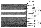
图1是表示本发明一实施方式中的透明导电性层叠体的截面示意图。FIG. 1 is a schematic cross-sectional view showing a transparent conductive laminate in one embodiment of the present invention.
图2是表示本发明一实施方式中的触摸面板的截面示意图。FIG. 2 is a schematic cross-sectional view showing a touch panel in one embodiment of the present invention.
图3是用于说明上述透明导电性层叠体中的导电性薄膜侧的硬度及弹性率的测定方法的说明图。FIG. 3 is an explanatory view for explaining a method of measuring the hardness and modulus of elasticity of the conductive film side in the transparent conductive laminate.
图4是用于说明本发明的实施例中的触摸面板的表面压力耐久性试验的截面示意图。4 is a schematic cross-sectional view illustrating a surface pressure durability test of a touch panel in an example of the present invention.
图5是表示实施例1中得到的触摸面板中的电压值与测定位置的关系的图表。5 is a graph showing the relationship between the voltage value and the measurement position in the touch panel obtained in Example 1. FIG.
符号说明Symbol Description
1 薄膜基材1 film substrate
2 导电性薄膜2 Conductive film
3 层叠透明基体3 Laminated transparent substrate
31、32基体薄膜31, 32 base film
41、42粘合剂层41, 42 Adhesive layer
5(51、52)电介质薄膜5 (51, 52) dielectric film
6 硬涂层6 hard coat
A 透明导电性层叠体A transparent conductive laminated body
s 隔离件s spacer
具体实施方式Detailed ways
以下,将在参照附图的同时对本发明的实施方式进行说明。其中,说明所不需要的部分省略,另外为了易于说明,存在扩大或缩小等而图示的部分。Hereinafter, embodiments of the present invention will be described with reference to the drawings. Among them, parts unnecessary for description are omitted, and for ease of description, there are parts shown enlarged or reduced in size.
图1是表示本实施方式中的透明导电性层叠体的一个例子的截面示意图。即,透明导电性层叠体A为下述结构:在透明的薄膜基材1的一个面上具有透明导电性薄膜2,在另一个面上经由透明的粘合剂层41贴合有层叠透明基体3。层叠透明基体3是将透明的基体薄膜31和透明的基体薄膜32经由透明的粘合剂层42层叠的层叠体。图1中,例示了层叠2层透明的基体薄膜的情况,但透明的基体薄膜的层叠只要是2层以上即可,可以为3层、4层,进而设为5层以上。通过设成这样的构造,可以提高面内耐久性。另外,图1是在层叠透明基体3的外表面设置有硬涂层(树脂层)6的情况。如图1所示,从薄膜基材1的一侧开始经由电介质薄膜5(第一透明电介质薄膜51及第二透明电介质薄膜52)设有透明导电性薄膜2。在图1中,电介质薄膜5是从薄膜基材1的一侧开始依次形成第一透明电介质薄膜51及第二透明电介质薄膜52的情形。通过设成这样的构造,可以进一步提高面内耐久性。FIG. 1 is a schematic cross-sectional view showing an example of a transparent conductive laminate in this embodiment. That is, the transparent conductive laminate A has a structure in which a transparent
作为上述薄膜基材1,没有特别限制,可以使用具有透明性的各种塑料薄膜。例如,作为其材料,可以举出聚酯系树脂、醋酸酯系树脂、聚醚砜系树脂、聚碳酸酯系树脂、聚酰胺系树脂、聚酰亚胺系树脂、聚烯烃系树脂、(甲基)丙烯酸系树脂、聚氯乙烯系树脂、聚偏二氯乙烯系树脂、聚苯乙烯系树脂、聚乙烯醇系树脂、聚芳酯系树脂、聚苯硫醚系树脂等。它们当中,特别优选聚酯系树脂、聚碳酸酯系树脂、聚烯烃系树脂。The above-mentioned
另外,可以举出日本特开2001-343529号公报(WO10/37007)中记载的高分子薄膜、例如含有(A)侧链具有取代和/或未取代的亚氨基的热塑性树脂与(B)侧链具有取代和/或未取代的苯基以及腈基的热塑性树脂的树脂组合物。具体可以使用含有由异丁烯及N-甲基马来酰亚胺组成的交替共聚物和丙烯腈·苯乙烯共聚物的树脂组合物的高分子薄膜。In addition, polymer films described in Japanese Patent Application Laid-Open No. 2001-343529 (WO10/37007), such as thermoplastic resins containing substituted and/or unsubstituted imino groups in (A) side chains and (B) side chains, can be mentioned. A resin composition of a thermoplastic resin having substituted and/or unsubstituted phenyl and nitrile groups in the chain. Specifically, a polymer film of a resin composition containing an alternating copolymer of isobutylene and N-methylmaleimide and an acrylonitrile-styrene copolymer can be used.
上述薄膜基材1的厚度优选为2~200μm的范围内。更优选为2~100μm的范围内。如果薄膜基材1的厚度小于2μm,则薄膜基材1的机械强度不足,将该薄膜基材1制成卷筒状,连续地形成导电性薄膜2、电介质薄膜5及粘合剂层41的操作将会变得困难。另一方面,当厚度超过200μm时,由于粘合剂层41的缓冲效果,将会无法实现导电性薄膜2的耐擦伤性或作为触摸面板用的触碰特性的提高。The thickness of the above-mentioned
上述薄膜基材1可以对表面预先实施溅射、电晕放电、火焰、紫外线照射、电子线照射、化成、氧化等蚀刻处理或底涂处理,从而提高设置于其上的导电性薄膜2或电介质薄膜5与上述薄膜基材1的密接性。另外,在设置导电性薄膜2或电介质薄膜5之前,也可以根据需要通过溶剂清洗及超声波清洗等施行除尘、清洁化。The above-mentioned
上述电介质薄膜5由第一透明电介质薄膜51及第二透明电介质薄膜52形成。上述电介质薄膜5优选将第一透明电介质薄膜51作为利用干式程序形成的相对折射率为1.6~1.9的SiOx膜(x为1.5以上且小于2)、将上述第二透明电介质薄膜52作为SiO2膜。The above-mentioned
电介质薄膜5可以使用上述材料,利用真空蒸镀法、溅射法、离子镀法等干式程序或湿法(涂刷法)等形成。电介质薄膜5的各厚度通常为1~300nm左右即可。The dielectric
上述SiOx膜(x为1.5以上且小于2)是通过干式程序形成的层。干式程序可以采用真空蒸镀、溅射、离子镀等方法。与利用涂刷聚硅氧烷系热固化性树脂或硅胶等的湿法形成SiOx膜的情形相比,可以提高面内耐久性。The aforementioned SiOx film (x is 1.5 or more and less than 2) is a layer formed by a dry process. Dry procedures can use methods such as vacuum evaporation, sputtering, and ion plating. In-plane durability can be improved compared to the case of forming theSiOx film by a wet method of applying a polysiloxane-based thermosetting resin or silica gel.
于薄膜基材1上设置上述SiOx膜(x为1.5以上且小于2),这是由于当使用聚对苯二甲酸乙二醇酯薄膜作为该薄膜基材1时,如果于薄膜基材1上直接仅设置SiO2膜作为结合层时,无法得到充分的密接性的缘故。因此,于薄膜基材1与SiO2膜之间设置SiOx膜作为第一透明电介质薄膜51,使用该SiOx膜作为粘接剂,确保充分的密接性。另外,由于SiO2为低折射率的材料,反射率低,其结果,可以实现高透光率。这样,SiO2膜特别地发挥作为导电性薄膜的结合层的效果,使面内耐久性提高。The above-mentioned SiOx film (x is more than 1.5 and less than 2) is provided on the
作为第一透明电介质薄膜51而设置的SiOx膜的厚度优选为1~30nm,更优选为1~15nm的范围。厚度小于1nm时,存在难以稳定地形成连续覆膜的倾向。厚度超过30nm时,例如通过进行环境可靠性试验等会导致反射及透过色调的变化。这是由于,在环境可靠性试验中,x接近2,通过从SiOx逐渐变化为SiO2,SiOx膜的折射率在约1.7~1.45的范围内变化的缘故。SiOx膜还是光学薄膜,光学薄膜的特性取决于各层的折射率及其厚度,已知厚度为25nm以下时,相对于折射率的变化,对光学特性的影响小。尚需说明的是,上述环境可靠性试验是指例如在80℃下的高温试验或在60℃/90%RH或85℃/85%RH等中的高温高湿试验等。The thickness of theSiOx film provided as the first transparent dielectric
上述SiOx膜的相对折射率为1.6~1.9的范围。通过处于上述范围内,例如将透明导电性层叠体A应用于触摸面板中时,可以提高面内耐久性。相对折射率小于1.6时,从上述面内耐久性的角度考虑并不优选。而相对折射率超过1.9的SiOx膜难以制备。The relative refractive index of the SiOx film is in the range of 1.6 to 1.9. By being within the above range, for example, when the transparent conductive laminate A is applied to a touch panel, in-plane durability can be improved. When the relative refractive index is less than 1.6, it is not preferable from the viewpoint of the above-mentioned in-plane durability. However, SiOx films with a relative refractive index exceeding 1.9 are difficult to prepare.
作为第二透明电介质薄膜52而设置的SiO2膜的厚度优选为10~70nm,更优选为10~65nm的范围。厚度小于10nm时,不易形成连续覆膜,耐擦伤性的提高不充分。厚度超过70nm时,透明性的提高不充分,有可能产生裂纹。The thickness of the SiO2 film provided as the second transparent dielectric
上述SiOx膜及SiO2膜的平均表面粗糙度分别优选为0.8~3.0nm的范围内。平均表面粗糙度小于0.8nm时,表面凹凸变得过于微细,防眩光性有可能下降。另外,如果在各种情况下都形成厚的导电性薄膜2,则表面电阻值也降的过低。另一方面,平均表面粗糙度超过3.0nm时,表面凹凸变得过大,可能难以得到稳定的表面电阻值。尚需说明的是,平均表面粗糙度是指,利用AFM(Atomic Force Microscope:原子间力显微镜)测定的「表面粗糙度(Ra)」。具体是指,使用SPI3800(Seiko Instruments社制)作为AFM,在模式为接触模式、短针为Si3N4制(弹簧常数0.09N/m)、扫描尺寸为1μm的条件下测定的值。The average surface roughness of the SiOx film and the SiO2 film is preferably within a range of 0.8 to 3.0 nm, respectively. When the average surface roughness is less than 0.8 nm, the surface unevenness becomes too fine, and the anti-glare property may decrease. In addition, if a thick conductive
作为上述导电性薄膜2的构成材料没有特别限制,例如优选使用含有氧化锡的氧化铟、含有锑的氧化锡等。其中导电性薄膜2特别优选由晶体粒径为200nm以下,更优选由50~150nm的、晶体含量超过50%的结晶质的铟锡氧化物构成的薄膜。这样,可以得到表面压力耐久性良好的薄膜。若晶体粒径大的晶体增多,则容易产生裂纹,表面压力耐久性趋于下降。尚需说明的是,晶体粒径定义为在透过型电子显微镜下观察到的多角形状或长圆形状的各区域中对角线或直径最大的粒径的平均值。晶体粒径的测定例如可以通过FE-TEM观察(株式会社日立制作所、HF-2000、加速电压200kV)等来进行。The constituent material of the conductive
导电性薄膜2的厚度优选为20~35nm,更优选为20~30nm的范围内。厚度小于20nm时,表面电阻变高,且难以形成连续覆膜。若超过35nm,则会发生透明性的下降等情况。The thickness of the conductive
需要说明的是,于薄膜基材1上经由SiOx膜设置导电性薄膜2作为第一透明电介质薄膜、然后经由SiO2膜设置导电性薄膜2作为第二透明电介质薄膜时,可以抑制其表面电阻的变化率,稳定性较以往出色。It should be noted that, on the
导电性薄膜2的形成方法没有特别限定,可以采用公知的方法。具体可以例示:真空蒸镀法、溅射法、离子镀法。另外,可以根据所需的膜厚采用适当的方法。The method for forming the conductive
在形成有上述导电性薄膜2的薄膜基材1的另一个面上,经由透明的粘合剂层41贴合层叠透明基体3。层叠透明基体3是将至少2张透明的基体薄膜利用透明的粘合剂层贴合的复合构造,由此可以提高表面压力耐久性。On the other surface of the
层叠透明基体3的厚度通常优选为90~300μm,更优选控制为100~250μm。另外,形成层叠透明基体3的各基体薄膜的厚度为10~200μm,更优选20~150μm,将在这些基体薄膜中包含透明的粘合剂层的作为层叠透明基体3的总厚度控制为处于上述范围。作为基体薄膜,可以举出与上述的薄膜基材1相同的材料。The thickness of the laminated
薄膜基材1与层叠透明基体3的贴合既可以在层叠透明基体3侧预先设置上述的粘合剂层41,在其上贴合上述薄膜基材1,也可以反过来,在薄膜基材1侧预先设置上述的粘合剂层41,在其上贴合层叠透明基体3。后者的方法中,由于可以将薄膜基材1制成卷筒状而连续地进行粘合剂层41的形成,因此在生产性方面更为有利。另外,也可以在薄膜基材1上,依次利用粘合剂层41、42贴合基体薄膜31、32,从而将层叠透明基体3层叠。而且,基体薄膜的层叠中所用的透明的粘合剂层(图1的粘合剂层42)可以使用与下述的透明的粘合剂层41相同的材料。The bonding of the
作为粘合剂层41,只要是具有透明性的材料,就可以没有特别限制地使用。具体来说,可以适当地选择使用丙烯酸系聚合物、硅系聚合物、聚酯、聚氨酯、聚酰胺、聚乙烯基醚、醋酸乙烯/氯乙烯共聚物、改性聚烯烃、环氧系、氟系、将天然橡胶、合成橡胶等橡胶系等聚合物作为基础聚合物的材料。特别是,从光学透明性出色、显示适当的润湿性、凝聚性和粘接性等的粘合特性、在耐气候性或耐热性等方面出色的方面考虑,可以优选使用丙烯酸系粘合剂。As the pressure-sensitive adhesive layer 41 , any material can be used without particular limitation as long as it has transparency. Specifically, acrylic polymers, silicon-based polymers, polyesters, polyurethanes, polyamides, polyvinyl ethers, vinyl acetate/vinyl chloride copolymers, modified polyolefins, epoxy-based, fluorine-based Materials that use rubber-based polymers such as natural rubber and synthetic rubber as the base polymer. In particular, acrylic adhesives can be preferably used in terms of excellent optical transparency, suitable adhesive properties such as wettability, cohesion, and adhesiveness, and excellent weather resistance and heat resistance. agent.
根据作为粘合剂层41的构成材料的粘合剂的种类不同,有时可以通过使用适当的粘合用底涂剂来提高抛锚固定力。因而,使用此种粘合剂时,优选使用粘合用底涂剂。Depending on the type of adhesive used as the constituent material of the adhesive layer 41 , it may be possible to improve the anchoring force by using an appropriate adhesive primer. Therefore, when using such an adhesive, it is preferable to use an adhesive primer.
作为上述粘合用底涂剂,只要是可以提高粘合剂的抛锚固定力的层即可,没有特别限制。具体而言,可以使用例如在同一分子内具有氨基、乙烯基、环氧基、巯基、氯基等反应性官能团和水解性的烷氧基甲硅烷基的硅烷系偶合剂;在同一个分子内具有含有钛的水解性亲水性基团和有机官能性基团的钛酸酯系偶合剂;和在同一个分子内具有含铝的水解性亲水性基团和有机官能性基团的铝酸酯系偶合剂等所谓偶合剂;环氧系树脂、异氰酸酯系树脂、氨基甲酸酯系树脂、氨基甲酸酯系树脂等具有有机反应性基团的树脂。其中,从工业上容易处理的观点来看,优选优选含有硅烷系偶合剂的层。The adhesive primer is not particularly limited as long as it is a layer that can improve the anchoring force of the adhesive. Specifically, for example, silane-based coupling agents having reactive functional groups such as amino groups, vinyl groups, epoxy groups, mercapto groups, and chlorine groups and hydrolyzable alkoxysilyl groups in the same molecule can be used; A titanate-based coupling agent having a titanium-containing hydrolyzable hydrophilic group and an organic functional group; and aluminum having an aluminum-containing hydrolyzable hydrophilic group and an organic functional group in the same molecule So-called coupling agents such as ester-based coupling agents; resins having organic reactive groups such as epoxy-based resins, isocyanate-based resins, urethane-based resins, and urethane-based resins. Among them, a layer containing a silane-based coupling agent is preferable from the viewpoint of industrial ease of handling.
另外,可以在上述粘合剂层41中含有对应基础聚合物的交联剂。另外,也可以根据需要在粘合剂层41中配合例如天然物或合成物的树脂类、玻璃纤维或玻璃珠、金属粉或其它无机粉末等组成的填充剂、颜料、着色剂、防氧化剂等适当的添加剂。另外,也可以形成含有透明微粒而显示光漫射性的粘合剂层41。In addition, a crosslinking agent corresponding to the base polymer may be contained in the above-mentioned pressure-sensitive adhesive layer 41 . In addition, fillers, pigments, colorants, antioxidants, etc. composed of natural or synthetic resins, glass fibers or glass beads, metal powders or other inorganic powders, etc., can also be mixed in the adhesive layer 41 as required. appropriate additives. In addition, the pressure-sensitive adhesive layer 41 may contain transparent fine particles and exhibit light diffusing properties.
而且,在上述透明微粒中,例如,可以使用平均粒径为0.5~20μm的二氧化硅、氧化钙、氧化铝、氧化钛、氧化锆、氧化锡、氧化铟、氧化镉、氧化锑等导电性的无机系微粒;或由类似聚甲基丙烯酸甲酯、聚氨酯之类的适当的聚合物组成的交联或者未交联的有机系微粒等适当的微粒的1种或2种以上。Moreover, in the above-mentioned transparent particles, for example, conductive materials such as silicon dioxide, calcium oxide, aluminum oxide, titanium oxide, zirconium oxide, tin oxide, indium oxide, cadmium oxide, and antimony oxide with an average particle diameter of 0.5 to 20 μm can be used. Inorganic microparticles; or one or more kinds of suitable microparticles such as crosslinked or uncrosslinked organic microparticles composed of suitable polymers such as polymethyl methacrylate and polyurethane.
上述粘合剂层41通常被作为将基础聚合物或其组合物溶解或分散到溶剂中的且固体成分浓度为10~50重量%左右的粘合剂溶液使用。作为上述溶剂,可以适当选择使用甲苯或醋酸乙酯等有机溶剂或水等与粘合剂的种类相对应的溶剂。The adhesive layer 41 is generally used as an adhesive solution in which a base polymer or a composition thereof is dissolved or dispersed in a solvent and has a solid content concentration of about 10 to 50% by weight. As said solvent, organic solvents, such as toluene and ethyl acetate, and solvents corresponding to the type of binder, such as water, can be suitably selected and used.
该粘合剂层41在粘接层叠透明基体3之后,利用其缓冲效果,具有提高设置在薄膜基材1的一个面的导电性薄膜的耐擦伤性或作为触摸面板用的触碰特性、即笔输入耐久性及表面压力耐久性的作用。从更好地发挥该作用的观点考虑,优选将粘合剂层41的弹性系数设定为1~100N/cm2的范围,将厚度设定为1μm以上,通常设定为5~100μm的范围。The pressure-sensitive adhesive layer 41 has the function of improving the scratch resistance of the conductive film provided on one side of the
在上述的弹性系数小于1N/cm2的情况下,粘合剂层41变为非弹性,因此,容易因加压变形而在薄膜基材1上、甚至在导电性薄膜2上产生凹凸。另外,容易产生自加工切截面的粘合剂的挤出等,并且降低导电性薄膜2的耐擦伤性或作为触摸面板用的触碰特性的提高效果。另一方面,弹性系数超过100N/cm2时,粘合剂层41变硬,不能期望其缓冲效果,因此,存在难以提高导电性薄膜2的耐擦伤性或作为触摸面板用的笔输入耐久性及表面压力耐久性的倾向。When the above-mentioned coefficient of elasticity is less than 1 N/cm2 , the adhesive layer 41 becomes inelastic, and thus tends to cause irregularities on the
另外,粘合剂层41的厚度小于1μm时,仍不能期望其缓冲效果,因此,存在难以提高导电性薄膜2的耐擦伤性或作为触摸面板用的笔输入耐久性及表面压力耐久性的倾向。相反地,使厚度过大时,则会损害透明性,或在粘合剂层41的形成或层叠透明基体3的贴合作业性甚至成本方面难以得到好的结果。In addition, when the thickness of the adhesive layer 41 is less than 1 μm, the cushioning effect cannot be expected, so it is difficult to improve the scratch resistance of the
借助此种粘合剂层41贴合的层叠透明基体3对薄膜基材1赋予良好的机械强度,除了笔输入耐久性及表面压力耐久性以外,尤其有助于防止卷曲等的发生。The laminated
使用上述隔离件转印粘合剂层41时,作为此种隔离件,例如优选使用在聚酯薄膜的至少与粘合剂层41粘接的面层叠移动防止层及/或脱模层而成的聚酯薄膜等。When transferring the adhesive layer 41 using the above-mentioned separator, it is preferable to use, as such a separator, a movement prevention layer and/or a release layer laminated on at least the surface of the polyester film that is bonded to the adhesive layer 41, for example. polyester film etc.
上述隔离件的总厚度优选为30μm以上,更优选为75~100μm的范围内。这是为了在形成粘合剂层41之后,以卷筒状态保管时,抑制由于进入卷筒间的异物等而设想发生的粘合剂层41的变形(打痕)。The total thickness of the separator is preferably 30 μm or more, more preferably within a range of 75 to 100 μm. This is to suppress deformation (scratch) of the adhesive layer 41 that is supposed to occur due to foreign matter or the like entering between the rolls when the adhesive layer 41 is formed and stored in a roll state.
作为上述移动防止层,可以使用用于防止聚酯薄膜中的移动成分、特别是聚酯等低分子量寡聚物成分的移动的适当材料来形成。作为移动防止层的形成材料,可以使用无机物或有机物、或它们的复合材料。移动防止层的厚度可以适当设定在0.01~20μm的范围。作为移动防止层的形成方法没有特别限定,例如使用涂刷法、喷涂法、旋涂法、在线涂布法等。另外,还可以采用真空蒸镀法、溅射法、离子镀法、喷射-热分解法、化学镀法、电镀法等。The anti-migration layer can be formed using an appropriate material for preventing migration of components in the polyester film, particularly low-molecular-weight oligomer components such as polyester. As a material for forming the anti-movement layer, an inorganic substance or an organic substance, or a composite material thereof can be used. The thickness of the anti-movement layer can be appropriately set in the range of 0.01 to 20 μm. The method for forming the anti-movement layer is not particularly limited, and for example, a brushing method, a spray coating method, a spin coating method, an in-line coating method, or the like is used. In addition, a vacuum evaporation method, a sputtering method, an ion plating method, a spray-pyrolysis method, an electroless plating method, an electroplating method, and the like can also be used.
可以形成由硅系、长链烷基系、氟系、硫化钼等适当的剥离剂制成的层作为上述脱模层。脱模层的厚度可以从脱模效果方面考虑来适当设定。通常,从柔软性等操作性的观点考虑,该厚度优选为20μm以下,更优选为0.01~10μm的范围内,特别优选为0.1~5μm的范围内。A layer made of a suitable release agent such as silicon-based, long-chain alkyl-based, fluorine-based, molybdenum sulfide, or the like can be formed as the above-mentioned release layer. The thickness of the release layer can be appropriately set in consideration of the release effect. Usually, the thickness is preferably 20 μm or less, more preferably within a range of 0.01 to 10 μm, particularly preferably within a range of 0.1 to 5 μm, from the viewpoint of handleability such as flexibility.
在上述涂刷法、喷涂法、旋涂法、在线涂布法中,可以使用丙烯酸系树脂、氨基甲酸酯系树脂、蜜胺系树脂、环氧系树脂等电离放射线固化型树脂、或者在上述树脂中混合了氧化铝、二氧化硅、云母等的物质。另外,在使用真空蒸镀法、溅射法、离子镀法、喷射-热分解法、化学镀法或电镀法时,可以使用金、银、铂、钯、铜、铝、镍、铬、钛、铁、钴或锡或它们的合金等组成的金属氧化物、碘化铜等组成的其它金属化合物。In the above-mentioned brushing method, spray coating method, spin coating method, and in-line coating method, ionizing radiation-curable resins such as acrylic resins, urethane resins, melamine resins, and epoxy resins can be used, or Alumina, silica, mica, etc. are mixed with the above-mentioned resin. In addition, gold, silver, platinum, palladium, copper, aluminum, nickel, chromium, titanium, etc. , iron, cobalt or tin or their alloys, metal oxides, copper iodide and other metal compounds.
另外,根据需要,也可以在上述层叠透明基体3的外表面(与粘合剂层41相反一侧的面),设置以提高辨识性为目的的防眩光处理层或防反射层,或者设置以保护外表面为目的的硬涂层(树脂层)6。防眩光处理层或防反射层还可以设置在于层叠透明基体3上设置的硬涂层6上。作为硬涂层6,例如可以优选使用蜜胺系树脂、氨基甲酸酯系树脂、醇酸系树脂、丙烯酸系树脂、硅系树脂等固化型树脂构成的固化覆膜。In addition, if necessary, an anti-glare treatment layer or an anti-reflection layer for the purpose of improving visibility may also be provided on the outer surface (the side opposite to the adhesive layer 41) of the above-mentioned laminated
作为防眩光处理层的构成材料,没有特别限定,可以使用例如电离放射线固化型树脂、热固化型树脂、热塑性树脂等。防眩光处理层的厚度优选0.1~30μm。如果薄于0.1μm,则担心硬度不足;如果厚于30μm,则防眩光处理层中将会出现裂纹、或者涂刷了防眩光处理层的层叠透明基体3整体发生卷曲。The constituent material of the anti-glare treatment layer is not particularly limited, and, for example, ionizing radiation-curable resins, thermosetting resins, thermoplastic resins, and the like can be used. The thickness of the anti-glare treatment layer is preferably 0.1 to 30 μm. If it is thinner than 0.1 μm, there may be insufficient hardness; if it is thicker than 30 μm, cracks will appear in the anti-glare treatment layer, or the entire laminated
作为防反射层,可以于上述硬涂层6上设置防反射层。光照射到物体上时,反复进行在其界面反射、在内部吸收、漫射等现象,透过至物体的背面。在图象显示装置上安装触摸面板时,作为降低图象辨识性的要因之一,可以举出:在空气与层叠透明基体3或硬涂层6界面的光的反射。作为降低其表面反射的方法,将严密控制了厚度及折射率的薄膜层叠于硬涂层6表面,使利用了光的干涉效果的入射光与反射光的逆转的位相相互抵消,从而体现防反射功能。As an antireflection layer, an antireflection layer may be provided on the above-mentioned
在基于光的干涉效果的防反射层的设计中,为了提高其干涉效果,而增大防反射层与硬涂层6的折射率差。通常,于基材上层叠2~5层光学薄膜(上述严密控制了厚度及折射率的薄膜)的多层防反射层中,通过形成多层规定的厚度的折射率不同的成分,可以在防反射层的光学设计中增加自由度、进一步提高防反射效果、分光反射特性在可见光线区域也变平。由于要求光学薄膜的各层的厚度精度,通常利用干式的真空蒸镀法、溅射法、CVD法等形成各层。In designing the antireflection layer based on the interference effect of light, the difference in refractive index between the antireflection layer and the
作为防反射层,使用氧化钛、氧化锆、氧化硅、氟化镁等。为了进一步体现防反射功能,优选使用氧化钛层与氧化硅层的层叠体。上述层叠体优选:于硬涂层6上形成折射率高的氧化钛层(折射率:约1.8)、于该氧化钛层上形成折射率低的氧化硅层(折射率:约1.45)的2层层叠体、以及于该2层层叠体上依次形成氧化钛层及氧化硅层的4层层叠体。通过设置这样的2层层叠体或4层层叠体的防反射层,可以均匀降低可见光线在波长区域(380~780nm)的反射。As the antireflection layer, titanium oxide, zirconium oxide, silicon oxide, magnesium fluoride, and the like are used. In order to further exhibit the antireflection function, it is preferable to use a laminated body of a titanium oxide layer and a silicon oxide layer. The above-mentioned laminate is preferably formed by forming a titanium oxide layer with a high refractive index (refractive index: about 1.8) on the
另外,通过在层叠透明基体3或硬涂层6上层叠单层的光学薄膜,也可以体现防反射效果。在使防反射层为单层的设计中,为了最大限度地引出防反射功能,必需增大防反射层与硬涂层6的折射率差。以上述防反射层的膜厚为d、折射率为n、入射光的波长为λ,防反射层的膜厚与其折射率之间满足nd=λ/4的关系。防反射层的折射率小于基材的折射率时,在上述关系式成立的条件中反射率变得最小。例如,防反射层的折射率为1.45时,相对于可见光线中波长550nm的入射光,使反射率最小的防反射层的膜厚为95nm。In addition, the antireflection effect can also be exhibited by laminating a single-layer optical film on the lamination
体现防反射止功能的可见光线的波长区域为380~780nm,特别是視感度高的波长区域为450~650nm的范围,通常进行使作为其中心波长的550nm的反射率最小的设计。The wavelength region of visible light that exhibits the anti-reflection function is 380-780nm, especially the wavelength region with high visual sensitivity is the range of 450-650nm, and it is usually designed to minimize the reflectance of the central wavelength of 550nm.
按照单层来设计防反射层时,其厚度精度并不如多层防反射膜的厚度精度一样严密,相对于设计厚度在±10%的范围、即设计波长为95nm时,只要在86nm~105nm的范围就可以没有问题地加以使用。由此,通常在单层防反射膜的形成中,采用湿式的喷泉涂布法(fountain coat)、模具涂布法、旋涂法、喷涂法、凹版涂布法、辊涂法、棒涂法等涂刷方法。When the anti-reflection layer is designed according to a single layer, its thickness accuracy is not as strict as that of the multi-layer anti-reflection film. Compared with the design thickness in the range of ±10%, that is, when the design wavelength is 95nm, as long as it is within the range of 86nm to 105nm The scope can then be used without problems. Therefore, in the formation of a single-layer antireflection film, wet fountain coating, die coating, spin coating, spray coating, gravure coating, roll coating, and bar coating are generally used. Wait for the brushing method.
作为硬涂层6的形成材料,优选使用例如蜜胺系树脂、氨基甲酸酯系树脂、醇酸系树脂、丙烯酸系树脂、硅系树脂等固化型树脂构成的固化覆膜。另外,硬涂层6的厚度优选0.1~30μm。厚度小于0.1μm时,硬度有时会不足。另外,厚度超过30μm时,硬涂层6中有时会产生裂纹、或者层叠透明基体3整体发生卷曲。As a material for forming the
另外,图1所示的透明导电性层叠体A在制作触摸面板时或者根据需要在100~150℃的范围内实施退火处理。因此,作为透明导电性层叠体A,优选具有100℃以上、进一步为150℃以上的耐热性。In addition, the transparent electroconductive laminate A shown in FIG. 1 is annealed in the range of 100-150 degreeC, when manufacturing a touch panel, or as needed. Therefore, as the transparent electroconductive laminate A, it is preferable to have heat resistance of 100° C. or higher, further 150° C. or higher.
透明导电性层叠体A中,作为层叠有导电性薄膜2的一侧的物性,优选导电性薄膜侧的硬度为2GPa以上、特别是3GPa以上。另外,优选导电性薄膜2侧的弹性率为8GPa以上、特别是10GPa以上。通过具有这样的物性,即使折弯透明导电性层叠体A,也不会出现导电性薄膜2中出现的裂纹、或者电阻值劣化等故障,作为耐弯曲性能高的透明导电性层叠体,可以适用于触摸面板等电致发光领域的基板中。另外,从耐裂纹性的观点考虑,上述导电性薄膜2侧的硬度的上限优选5GPa以下、进一步为4GPa以下;同样从耐裂纹性的观点考虑,上述导电性薄膜2侧的弹性率优选20GPa以下、进一步为16GPa以下。In the transparent electroconductive laminate A, as physical properties of the side on which the electroconductive
上述导电性薄膜2侧的硬度及弹性率通过压痕(indentation)试验(压头压入试验),例如使用扫描型探针显微镜(JEOL.LTD/日本电子:JSPM-4200)等可以测定(参照图3)。在薄膜硬度测定中,通常必需使压头的压入深度止于膜厚深度的10分之1左右。The hardness and elastic modulus of the above-mentioned
在压痕试验中,将受试体(即透明导电性层叠体A的导电性薄膜2侧)固定在试样台20上,在此状态下对受试体的大致中心部分施加负荷,压入压头21,得到压痕曲线(负荷-压入深度曲线)。根据此时的最大负荷Pmax、压头21与受试体间的接触投影面积A之比,由下式(1)求出受试体的硬度H。另外,根据压痕曲线的除荷曲线的初期斜率S,由下式(2)求出受试体的复合弹性率Er。并且,根据压头21的杨氏模量Ei、压头21的泊松比vi、受试体的泊松比vs,由下式(3)求出受试体的杨氏模量Es。In the indentation test, the test object (that is, the
其中,下式(2)中β为常数。另外,压头为金刚石,其杨氏模量Ei为1,140GPa、泊松比为0.07。Wherein, β in the following formula (2) is a constant. In addition, the indenter is diamond, and its Young's modulus Ei is 1,140 GPa, and its Poisson's ratio is 0.07.
【数学式1】【Mathematical formula 1】
H=P max/Λ … (1)H=P max/Λ … (1)
Er=1/{(1-vs2)/Es+(1-vi2)/Ei} … (3)Er=1/{(1-vs2)/Es+(1-vi2)/Ei} … (3)
其中,由于作为受试体的导电性薄膜的泊松比vs不清楚,因此将上述复合弹性率Er作为本发明中所说的弹性率。关于测定的细节,例如如W.C.Oliver and G.M.Phar,J.Meter.Res.,Vol.7,No.6,June 1992或Handbook of Micro/Nanotribology等中所记载的那样,可以利用公知的方法进行测定。Here, since the Poisson's ratio vs. of the conductive thin film as a test object is unclear, the above-mentioned complex elastic modulus Er is used as the elastic modulus in the present invention. As for the details of the measurement, for example, as described in W.C.Oliver and G.M.Phar, J.Meter.Res., Vol.7, No.6, June 1992 or Handbook of Micro/Nanotribology, etc., it can be measured by a known method .
接下来,对本实施方式中的触摸面板进行说明。图2是概略地显示本实施方式中的触摸面板的截面示意图。如同图所示,触摸面板为上述透明导电性层叠体A与下侧基板A′经由隔离件s而对置的结构。Next, the touch panel in this embodiment will be described. FIG. 2 is a schematic cross-sectional view schematically showing the touch panel in this embodiment. As shown in the figure, the touch panel has a structure in which the above-mentioned transparent conductive laminate A and the lower substrate A' face each other via a spacer s.
下侧基板A′为于其它透明基体1′上层叠其它导电性薄膜2′的构成。但是,本发明并不受限于此,例如也可以将透明导电性层叠体A用作下侧基板A′。作为其它透明基体1′的构成材料,基本上使用玻璃板或与层叠透明基体3相同的材料。另外,关于其厚度等也可以和层叠透明基体3相同。作为其它导电性薄膜2′的构成材料,基本上可以使用与导电性薄膜2相同的材料。另外,关于其厚度等也可以与导电性薄膜2相同。The lower substrate A' is formed by laminating another conductive thin film 2' on another transparent base 1'. However, the present invention is not limited thereto, and for example, the transparent conductive laminate A may be used as the lower substrate A'. As a constituent material of the other transparent base 1', basically a glass plate or the same material as the laminated
作为隔离件s,只要是绝缘性的隔离件即可,没有特别限定,可以使用以往公知的各种隔离件。对隔离件s的制造方法、尺寸、配置位置、数量没有特别限定。另外,隔离件s的形状可以采用近球形的形状或多角形状等以往公知的形状。The spacer s is not particularly limited as long as it is an insulating spacer, and various conventionally known spacers can be used. The manufacturing method, size, arrangement position, and number of the spacers s are not particularly limited. In addition, the shape of the spacer s may be a conventionally known shape such as a nearly spherical shape or a polygonal shape.
图2所示的触摸面板作为透明开关基体而发挥作用,即,在从透明导电性层叠体A侧使用输入笔等反抗隔离件S的弹力进行按压触碰时,导电性薄膜2、2’之间接触,成为电路的ON状态,当解除上述按压时,则回到原来的OFF状态。此时,触摸面板由于其导电性薄膜2在耐擦伤性或笔输入耐久性、表面压力耐久性等方面出色,可以长时间稳定地维持上述功能。The touch panel shown in FIG. 2 functions as a transparent switch base, that is, when the touch panel is pressed and touched from the side of the transparent conductive laminate A against the elastic force of the spacer S by using a stylus or the like, the
【实施例】【Example】
以下,利用实施例来详细说明本发明,但本发明只要不超出其要旨,并不限于以下的实施例。另外,各例中的“份”只要没有特别说明,则均为重量基准。Hereinafter, the present invention will be described in detail using examples, but the present invention is not limited to the following examples unless the gist is exceeded. In addition, "parts" in each example are based on weight unless otherwise specified.
(实施例1)(Example 1)
[电介质薄膜的形成][Formation of Dielectric Thin Film]
在由厚25μm的聚对苯二甲酸乙二醇酯薄膜(以下称作PET薄膜)制成的薄膜基材的一个面上,利用真空蒸镀法形成SiOx膜(相对折射率1.80、厚度15nm)。然后,利用真空蒸镀法于SiOx膜上形成SiO2膜(相对折射率1.46、厚度30nm)。On one side of a film substrate made of a polyethylene terephthalate film (hereinafter referred to as PET film) with a thickness of 25 μm, a SiOx film (relative refractive index 1.80, thickness 15 nm) was formed by vacuum evaporation. ). Then, a SiO2 film (relative refractive index 1.46, thickness 30 nm) was formed on the SiOx film by a vacuum evaporation method.
[导电性薄膜的形成][Formation of conductive thin film]
然后,在氩气95%与氧气5%组成的0.4Pa的气氛中,使用由氧化铟95重量%、氧化锡5重量%的烧结体材料,利用反应溅射法在SiO2膜上形成厚25nm的ITO膜(导电性薄膜、相对折射率2.00)。利用150℃×1小时的加热处理使ITO膜结晶化。Then, in an atmosphere of 0.4 Pa consisting of 95% argon and 5% oxygen, a sintered body material consisting of 95% by weight of indium oxide and 5% by weight of tin oxide was used to form a 25nm-thick layer on theSiO2 film by reactive sputtering. ITO film (conductive thin film, relative refractive index 2.00). The ITO film was crystallized by heat treatment at 150° C. for 1 hour.
[硬涂层的形成][Formation of hard coat layer]
作为硬涂层的形成材料,在丙烯酸·氨基甲酸酯系树脂(大日本油墨化学(株)制的UNIDIC 17-806)100份中,添加作为光聚合引发剂的羟基环己基苯基酮(千叶特殊化学药品(Ciba Specialty Chemicals)公司制的Irgacure 184)5份,配制成稀释至30重量%浓度的甲苯溶液。As a material for forming the hard coat layer, hydroxycyclohexyl phenyl ketone ( 5 parts of Irgacure 184 manufactured by Chiba Specialty Chemicals (Ciba Specialty Chemicals), prepared as a toluene solution diluted to a concentration of 30% by weight.
在厚125μm的PET薄膜构成的基体薄膜的一个面,涂布该硬涂层的形成材料,在100℃下干燥3分钟。然后立即用2个臭氧型高压汞灯(能量密度80W/cm2,15cm聚光型)进行紫外线照射,形成厚度为5μm的硬涂层。The material for forming the hard coat layer was applied to one surface of a base film made of a PET film having a thickness of 125 μm, and dried at 100° C. for 3 minutes. Immediately thereafter, two ozone-type high-pressure mercury lamps (energy density 80 W/cm2 , 15 cm concentrating type) were irradiated with ultraviolet rays to form a hard coat layer with a thickness of 5 μm.
[层叠透明基体的制作][Production of laminated transparent substrate]
接着,在上述基体薄膜的与硬涂层形成面相反一侧的面上,形成厚约20μm的弹性系数为10N/cm2的透明的丙烯酸系的粘合剂层。作为粘合剂层组合物,使用在由丙烯酸丁酯、丙烯酸和醋酸乙烯酯的重量比为100∶2∶5的丙烯酸系共聚物100份中配合1份异氰酸酯系交联剂而成的粘合剂层组合物。在上述粘合剂层侧贴合由厚25μm的PET薄膜构成的基体薄膜,制作具有两张PET薄膜的层叠透明基体。Next, a transparent acrylic pressure-sensitive adhesive layer having a thickness of about 20 μm and an elastic modulus of 10 N/cm2 was formed on the surface of the base film opposite to the surface on which the hard coat layer was formed. As the adhesive layer composition, an adhesive agent obtained by mixing 1 part of an isocyanate-based crosslinking agent with 100 parts of an acrylic copolymer composed of butyl acrylate, acrylic acid and vinyl acetate at a weight ratio of 100:2:5 was used. Agent layer composition. A base film made of a PET film having a thickness of 25 μm was bonded to the adhesive layer side to prepare a laminated transparent base having two PET films.
[透明导电性层叠体的制作][Production of transparent conductive laminate]
在上述层叠透明基体的与硬涂层形成面相反一侧的面上,用与上述相同的条件形成粘合剂层,将该粘合剂层面和薄膜基材(没有形成导电性薄膜的一侧的面)贴合,这样就制成本实施例中的透明导电性层叠体。On the surface of the above-mentioned laminated transparent substrate opposite to the hard coat layer formation surface, an adhesive layer is formed under the same conditions as above, and the adhesive layer and the film substrate (the side where the conductive film is not formed) surface) and bonded together, the transparent conductive laminate in this example was produced.
实施例2Example 2
[电介质薄膜的形成][Formation of Dielectric Thin Film]
在由厚25μm的PET薄膜制成的薄膜基材的一个面,利用有机材料形成厚200nm的电介质薄膜。形成由蜜胺树脂∶烷基醇酸树脂∶有机硅烷缩合物=2∶2∶1(重量比)的热固化性树脂制成的固化覆膜(相对折射率n=1.54)作为该电介质薄膜。On one side of a film substrate made of a PET film with a thickness of 25 μm, a dielectric thin film with a thickness of 200 nm was formed using an organic material. As the dielectric film, a cured film (relative refractive index n=1.54) made of a thermosetting resin of melamine resin:alkyl alkyd resin:organosilane condensate=2:2:1 (weight ratio) was formed.
接下来,在电介质薄膜上,利用氧化硅涂覆法形成了湿SiO2膜。即,涂布以使固体成分浓度达到2%的方式将硅胶(Colcoat公司制的「ColcoatP」)用乙醇稀释了的材料,在150℃干燥2分钟后,将其固化,形成了厚30nm的湿SiO2膜(相对折射率为1.46)。Next, on the dielectric thin film, a wet SiO2 film was formed using the silicon oxide coating method. That is, a material in which silica gel ("Colcoat P" manufactured by Colcoat Co., Ltd.) was diluted with ethanol was applied so that the solid content concentration became 2%, and after drying at 150° C. for 2 minutes, it was cured to form a wet coating with a thickness of 30 nm.SiO2 film (relative refractive index 1.46).
[透明导电性层叠体的制作][Production of transparent conductive laminate]
在实施例1中,除了进行上述操作作为[电介质薄膜的形成]以外,与实施例1同样操作,制作了透明导电性层叠体。In Example 1, except having performed the above-mentioned operation as [formation of dielectric thin film], it carried out similarly to Example 1, and produced the transparent electroconductive laminated body.
实施例3Example 3
[电介质薄膜的形成][Formation of Dielectric Thin Film]
在实施例2中,除了利用有机材料形成的电介质薄膜的厚度为35nm、未形成湿SiO2膜以外,进行与实施例2相同的操作,制作电介质薄膜。In Example 2, except that the thickness of the dielectric thin film formed of an organic material was 35 nm, and no wet SiO2 film was formed, the same operation as in Example 2 was carried out to produce a dielectric thin film.
[透明导电性层叠体的制作][Production of transparent conductive laminate]
在实施例2中,除了进行上述操作作为[电介质薄膜的形成]以外,与实施例2同样操作,制作了透明导电性层叠体。In Example 2, except having performed the above-mentioned operation as [formation of dielectric thin film], it carried out similarly to Example 2, and produced the transparent electroconductive laminated body.
实施例4Example 4
[电介质薄膜的形成][Formation of Dielectric Thin Film]
在实施例1中,除了使SiO2膜的厚度为60μm以外,进行与实施例1相同的操作,制作电介质薄膜。In Example 1, a dielectric thin film was produced in the same manner as in Example 1 except that the thickness of the SiO2 film was 60 μm.
[透明导电性层叠体的制作][Production of transparent conductive laminate]
在实施例1中,除了进行上述操作作为[电介质薄膜的形成]以外,与实施例1同样操作,制作了透明导电性层叠体。In Example 1, except having performed the above-mentioned operation as [formation of dielectric thin film], it carried out similarly to Example 1, and produced the transparent electroconductive laminated body.
实施例5Example 5
[电介质薄膜的形成][Formation of Dielectric Thin Film]
在实施例2中,除了使利用有机材料形成的电介质薄膜的厚度为150μm以外,进行与实施例2相同的操作,制作电介质薄膜。In Example 2, the dielectric thin film was produced in the same manner as in Example 2 except that the thickness of the dielectric thin film formed of an organic material was 150 μm.
[透明导电性层叠体的制作][Production of transparent conductive laminate]
在实施例2中,除了进行上述操作作为[电介质薄膜的形成]以外,与实施例2同样操作,制作了透明导电性层叠体。In Example 2, except having performed the above-mentioned operation as [formation of dielectric thin film], it carried out similarly to Example 2, and produced the transparent electroconductive laminated body.
比较例1Comparative example 1
在实施例2中,除了未使用层叠透明基体,而是作为透明基体,使用了在由厚125μm的PET薄膜构成的基体薄膜上形成了硬涂层的材料(在实施例1的层叠透明基体中,未贴合由厚25μm的PET薄膜构成的基体薄膜的材料)以外,与实施例2相同地制作了透明导电性层叠体。In Example 2, instead of using the laminated transparent base, a material in which a hard coat layer was formed on a base film made of a PET film with a thickness of 125 μm was used as the transparent base (in the laminated transparent base of Example 1 , a transparent conductive laminate was produced in the same manner as in Example 2, except that a base film made of a PET film with a thickness of 25 μm was not bonded).
比较例2Comparative example 2
在实施例3中,除了未使用层叠透明基体,而是作为透明基体,使用了在由厚125μm的PET薄膜构成的基体薄膜上形成了硬涂层的材料(在实施例1的层叠透明基体中,未贴合由厚25μm的PET薄膜构成的基体薄膜的材料)以外,与实施例3相同地制作了透明导电性层叠体。In Example 3, instead of using the laminated transparent base, a material in which a hard coat layer was formed on a base film made of a PET film with a thickness of 125 μm was used as the transparent base (in the laminated transparent base of Example 1 , a transparent conductive laminate was produced in the same manner as in Example 3, except that a base film made of a PET film with a thickness of 25 μm was not bonded).
(触摸面板的制作)(production of touch panel)
以实施例及比较例中得到的各透明导电性层叠体为面板,作为另一个面板(下侧基板),使用利用与上述相同的方法于玻璃板上形成了厚30nm的ITO薄膜的透明导电性玻璃,将该两块面板经由10μm的隔离件进行对向配置使ITO薄膜彼此相对,分别制作作为开关骨架体的触摸面板。尚需说明的是,两块面板的各ITO薄膜在上述对向配置之前,按照相互垂直的方式预先形成有银电极。Each of the transparent conductive laminates obtained in Examples and Comparative Examples was used as a panel, and as the other panel (lower substrate), a transparent conductive laminate in which a 30 nm-thick ITO film was formed on a glass plate by the same method as above was used. Glass, these two panels were arranged facing each other through a 10 μm spacer so that the ITO films faced each other, and each touch panel as a switch skeleton was produced. It should be noted that, before the above-mentioned opposing arrangement of the ITO thin films of the two panels, silver electrodes are pre-formed in a manner perpendicular to each other.
(折射率)(refractive index)
至于SiOx膜、SiO2膜、ITO膜等的折射率,使用ATAGO公司制的阿贝折射率计,对各种测定面入射测定光,利用该折射计所示的规定的测定方法进行测定。The refractive index of the SiOx film, SiO2 film, ITO film, etc. was measured using an Abbe refractometer manufactured by ATAGO Co., Ltd., and measuring light was incident on various measurement surfaces, and measured by a predetermined measurement method shown in the refractometer.
(各层的厚度)(thickness of each layer)
关于薄膜基材、基体薄膜、硬涂层、粘合剂层等具有1μm以上的厚度的层,利用日本三丰制Microgag(マイクロゲ一ジ)式厚度计进行测定。在硬涂层、粘合剂层等难以直接计测厚度的层的情况下,测定设有各层的基材的总厚度,通过扣除基材的厚度,算出各层的膜厚。A layer having a thickness of 1 μm or more, such as a film base material, a base film, a hard coat layer, and an adhesive layer, was measured using a Microgag thickness gauge manufactured by Mitutoyo Corporation. In the case of a layer whose thickness is difficult to measure directly, such as a hard coat layer or an adhesive layer, the total thickness of the substrate provided with each layer is measured, and the film thickness of each layer is calculated by subtracting the thickness of the substrate.
至于SiOx膜、SiO2膜、ITO膜等的厚度,使用大塚电子(株)制的瞬间多重测光系统MCPD2000(商品名),基础地算出来自干涉光谱的波形。As for the thickness of theSiOx film, SiO2 film, ITO film, etc., the waveform derived from the interference spectrum was basically calculated using an instantaneous multiple photometry system MCPD2000 (trade name) manufactured by Otsuka Electronics Co., Ltd.
(导电性薄膜侧的硬度及弹性率)(Hardness and modulus of elasticity on the conductive film side)
利用压痕试验,按照本文详述的方法测定导电性薄膜侧的硬度及弹性率。即,如上述图3所示,将标准样品(溶融二氧化硅)固定在试样台上,在此状态下对标准样品的大致中心部分施加负荷沿垂直方向压入压头。标准样品中压头接触时的最大压入深度hc与接触投影面积A的关系由下式表示。Using an indentation test, the hardness and modulus of elasticity of the conductive film side were determined according to the method detailed herein. That is, as shown in FIG. 3 above, the standard sample (fused silica) is fixed on the sample stage, and in this state, a load is applied to the approximate center of the standard sample and pressed into the indenter in the vertical direction. The relationship between the maximum indentation depth hc and the contact projected area A when the indenter is in contact with the standard sample is expressed by the following formula.
【数学式2】【Mathematical formula 2】
A=24.5hc2=C0hc2+C1hc+C2hc1/2+C3hc1/4+C4hc1/8+C5hc1/10A=24.5hc2 =C0 hc2 +C1 hc+C2 hc1/2 +C3 hc1/4 +C4 hc1/8 +C5 hc1/10
并且,使用上述数式(1)~(3)算出C0~C5。计算时,在负荷为20N、50N、80N、100N、150N、200N的6种条件下,分别用3秒钟沿垂直方向压入一次压头(压头压入),每个样品测定5次,求出平均值。在各次的测定中充分确保测定位置的距离,使不产生压痕的影响。另外,在各负荷下按照硬度H为10GPa、弹性率Er为70GPa进行计算。Then, C0 to C5 are calculated using the above formulas (1) to (3). When calculating, under the six conditions of loads of 20N, 50N, 80N, 100N, 150N, and 200N, it takes 3 seconds to press the indenter in the vertical direction (pressing the indenter), and each sample is measured 5 times. Find the average. In each measurement, the distance of the measurement position is sufficiently secured so that the influence of the indentation does not occur. In addition, the calculation was performed with the hardness H being 10 GPa and the elastic modulus Er being 70 GPa under each load.
接下来,以各实施例及比较例中得到的透明导电性层叠体作为受试体,测定各自的硬度及弹性率。将受试体固定在试样台上,使导电性薄膜(ITO薄膜)成为上侧。在如此固定的状态下,对导电性薄膜侧的大致中心部分以负荷20μN、用3秒钟沿垂直方向压入一次压头(压头压入),每个样品测定5次,求出平均值。Next, the respective hardness and modulus of elasticity were measured using the transparent conductive laminates obtained in the respective Examples and Comparative Examples as test objects. The test object was fixed on the sample stand with the conductive film (ITO film) on the upper side. In such a fixed state, press the indenter (indenter indentation) once in the vertical direction with a load of 20 μN on the approximate center of the conductive film side for 3 seconds, measure each
(表面电阻值)(surface resistance value)
使用二端子法,测定各触摸面板中的ITO膜的表面电阻值(Ω/□)。The surface resistance value (Ω/□) of the ITO film in each touch panel was measured using a two-probe method.
<光的透过率><Light transmittance>
使用岛津制作所制的分光分析装置UV-240,测定了光波长550nm下的可见光线透过率。Visible light transmittance at a light wavelength of 550 nm was measured using a spectroscopic analyzer UV-240 manufactured by Shimadzu Corporation.
<表面压力耐久性><Surface Pressure Durability>
如图4所示,在用负荷2kg挤压表面压力耐久性试验用夹具(接地直径Φ20mm)的状态下(夹具在与触摸面板接地时的摩擦系数为0.7~1.3),使夹具相对于各触摸面板滑动,在规定条件下测定滑动之后的直线性,评价表面压力耐久性。滑动动作在透明导电性层叠体侧,是在与触摸面板的周边部相距5mm以上的范围内的区域进行的。另外,滑动条件为,将滑动次数设为100次,将触摸面板的间距设为100μm。As shown in Figure 4, in the state where the surface pressure durability test jig (ground diameter Φ20 mm) is pressed with a load of 2 kg (the friction coefficient of the jig when it is in contact with the touch panel is 0.7 to 1.3), the jig is pressed against each touch panel. The panel is slid, and the linearity after sliding is measured under specified conditions to evaluate the surface pressure durability. The sliding operation was performed in a region within a range of 5 mm or more from the peripheral portion of the touch panel on the side of the transparent conductive laminate. In addition, the slide conditions were such that the number of slides was 100 and the pitch of the touch panel was 100 μm.
直线性的测定如下所述。即,在透明导电性层叠体中,施加5V的电压,将测定开始位置A的输出电压设为EA、测定结束位置B的输出电压设为EB、测定点的输出电压设为EX、理论值设为EXX时,则直线性可由下面的方法得到。The measurement of linearity is as follows. That is, a voltage of 5 V was applied to the transparent conductive laminate, and the output voltage at the measurement start position A was EA , the output voltage at the measurement end position B was EB , and the output voltage at the measurement point was EX , When the theoretical value is set to EXX , the linearity can be obtained by the following method.
即,在各触摸面板的滑动之后,在透明导电性层叠体中,施加5V的电压,将测定开始位置A的输出电压设为EA、测定结束位置B的输出电压设为EB、测定点的输出电压设为EX、理论值设为EXX时,可用下述公式计算得到直线性。图5中给出表示在实施例1中得到的触摸面板中的电压值与测定位置之间的关系的图表。同图所示的实线表示实测值,虚线表示理论值。由得到的直线性的值来评价表面压力耐久性。结果见下述表1。That is, after the sliding of each touch panel, a voltage of 5 V was applied to the transparent conductive laminate, and the output voltage at the measurement start position A was EA , the output voltage at the measurement end position B was EB , and the measurement point When the output voltage is set as EX and the theoretical value is set as EXX , the linearity can be calculated by the following formula. FIG. 5 is a graph showing the relationship between the voltage value in the touch panel obtained in Example 1 and the measurement position. The solid line shown in the figure shows the measured value, and the dotted line shows the theoretical value. The surface pressure durability was evaluated from the obtained linearity value. The results are shown in Table 1 below.
[数学式3][mathematical formula 3]
EXX(理论值)=X·(EB-EA)/(B-A)+EAEXX (theoretical value)=X·(EB -EA )/(BA)+EA
直线性(%)={(EXX-EX)/(EB-EA)}×100Linearity (%)={(EXX -EX )/(EB -EA )}×100
[表1][Table 1]

(结果)(result)
如下述表1所示,如果是实施例的触摸面板,则可知在表面压力耐久性方面出色。特别是,可以通过像实施例1那样作为电介质薄膜使用特定的薄膜来提高表面压力耐久性。As shown in Table 1 below, the touch panels of the examples were found to be excellent in surface pressure durability. In particular, surface pressure durability can be improved by using a specific film as the dielectric film as in Example 1.
Claims (9)
Translated fromChineseApplications Claiming Priority (3)
| Application Number | Priority Date | Filing Date | Title |
|---|---|---|---|
| JP212347/2006 | 2006-08-03 | ||
| JP2006212347AJP5116004B2 (en) | 2006-08-03 | 2006-08-03 | Transparent conductive laminate and touch panel provided with the same |
| PCT/JP2007/061558WO2008015840A1 (en) | 2006-08-03 | 2007-06-07 | Transparent conductive laminate and touch panel equipped with it |
Related Child Applications (1)
| Application Number | Title | Priority Date | Filing Date |
|---|---|---|---|
| CN201110139234.0ADivisionCN102298985B (en) | 2006-08-03 | 2007-06-07 | Transparent conductive laminated body and touch panel comprising the laminated body |
Publications (2)
| Publication Number | Publication Date |
|---|---|
| CN101490768A CN101490768A (en) | 2009-07-22 |
| CN101490768Btrue CN101490768B (en) | 2012-04-25 |
Family
ID=38997024
Family Applications (2)
| Application Number | Title | Priority Date | Filing Date |
|---|---|---|---|
| CN201110139234.0AActiveCN102298985B (en) | 2006-08-03 | 2007-06-07 | Transparent conductive laminated body and touch panel comprising the laminated body |
| CN2007800273948AActiveCN101490768B (en) | 2006-08-03 | 2007-06-07 | Transparent conductive laminated body and touch panel comprising the laminated body |
Family Applications Before (1)
| Application Number | Title | Priority Date | Filing Date |
|---|---|---|---|
| CN201110139234.0AActiveCN102298985B (en) | 2006-08-03 | 2007-06-07 | Transparent conductive laminated body and touch panel comprising the laminated body |
Country Status (7)
| Country | Link |
|---|---|
| US (2) | US8048512B2 (en) |
| EP (1) | EP2048672B1 (en) |
| JP (1) | JP5116004B2 (en) |
| KR (2) | KR101175968B1 (en) |
| CN (2) | CN102298985B (en) |
| TW (2) | TW201201224A (en) |
| WO (1) | WO2008015840A1 (en) |
Families Citing this family (45)
| Publication number | Priority date | Publication date | Assignee | Title |
|---|---|---|---|---|
| US20080113877A1 (en)* | 2006-08-16 | 2008-05-15 | Intematix Corporation | Liquid solution deposition of composition gradient materials |
| JP5072033B2 (en)* | 2008-03-24 | 2012-11-14 | 三菱樹脂株式会社 | Laminated polyester film for transparent conductive film |
| JP5160325B2 (en)* | 2008-07-16 | 2013-03-13 | 日東電工株式会社 | Transparent conductive film and touch panel |
| JP5095814B2 (en) | 2008-08-25 | 2012-12-12 | 日本写真印刷株式会社 | Touch input device and electronic device |
| KR101022030B1 (en)* | 2009-04-20 | 2011-03-16 | 이미지랩(주) | Resistive touch sheet and manufacturing method thereof |
| JP5518374B2 (en)* | 2009-05-18 | 2014-06-11 | デクセリアルズ株式会社 | Adhesive layer for suppressing oligomer precipitation of laminated laminated PET film |
| US8597963B2 (en)* | 2009-05-19 | 2013-12-03 | Intematix Corporation | Manufacture of light emitting devices with phosphor wavelength conversion |
| US20110027561A1 (en)* | 2009-07-29 | 2011-02-03 | Cheng-Chieh Chang | Optical film structure and display device |
| KR20110038517A (en)* | 2009-10-08 | 2011-04-14 | 엘지이노텍 주식회사 | Surface member for touch panel and manufacturing method therefor |
| JP5556436B2 (en)* | 2009-10-13 | 2014-07-23 | 東洋紡株式会社 | Transparent conductive laminated film, transparent conductive laminated sheet, and touch panel |
| CN102214028B (en)* | 2010-04-06 | 2014-07-16 | 晨星软件研发(深圳)有限公司 | Gesture recognition method and device for touch panel |
| KR101127412B1 (en)* | 2010-04-21 | 2012-03-26 | 이미지랩(주) | Touch panel having improved visibility and manufacturing method of the same |
| JP5786403B2 (en)* | 2011-03-29 | 2015-09-30 | 凸版印刷株式会社 | Transparent conductive laminate and touch panel using the same |
| JP5535399B2 (en)* | 2011-04-06 | 2014-07-02 | 帝人株式会社 | Transparent conductive laminate and transparent touch panel |
| JP2013012020A (en)* | 2011-06-29 | 2013-01-17 | Panasonic Corp | Touch panel |
| CN102984929B (en)* | 2011-09-07 | 2015-07-08 | 港易有限公司 | Radiation-proof laminate for electronic device and method for embedding the laminate in case |
| TW201337705A (en)* | 2011-10-25 | 2013-09-16 | Unipixel Displays Inc | Polarizer resistive touch screen |
| CN103959216A (en)* | 2011-10-25 | 2014-07-30 | 尤尼皮克塞尔显示器有限公司 | Polarizer capacitive touch screen |
| KR20140096306A (en)* | 2011-10-25 | 2014-08-05 | 유니-픽셀 디스플레이스, 인코포레이티드 | Method of manufacturing a resistive touch sensor circuit by flexographic printing |
| TW201332782A (en)* | 2011-10-25 | 2013-08-16 | Unipixel Displays Inc | Method of manufacturing a capacative touch sensor circuit using flexographic printing |
| JP5281216B1 (en)* | 2011-11-11 | 2013-09-04 | 株式会社カネカ | Substrate with transparent electrode, method for manufacturing the same, and touch panel |
| KR101974478B1 (en)* | 2012-01-09 | 2019-08-26 | 삼성디스플레이 주식회사 | Transparent laminate, window panel for display device and display device including the window panel |
| WO2013141318A1 (en)* | 2012-03-22 | 2013-09-26 | リンテック株式会社 | Transparent conductive laminate and electronic device or module |
| US9253892B2 (en)* | 2012-04-13 | 2016-02-02 | Wistron Corporation | Peripheral circuit of touch panel and manufacturing method thereof |
| US9696751B2 (en) | 2012-05-17 | 2017-07-04 | Kaneka Corporation | Substrate with transparent electrode, method for manufacturing same, and touch panel |
| EP2853386B1 (en)* | 2012-05-21 | 2017-10-25 | Toray Industries, Inc. | Substrate and touch panel member using same |
| BE1020722A3 (en) | 2012-06-01 | 2014-04-01 | Unilin Bvba | PANEL FOR FORMING A FLOOR COVERING AND METHOD FOR MANUFACTURING SUCH PANELS. |
| CN103455191A (en)* | 2012-06-05 | 2013-12-18 | 昆山雅森电子材料科技有限公司 | Composite film structure and touch panel with same |
| CN104334342B (en)* | 2012-06-06 | 2016-03-09 | 东丽株式会社 | The manufacture method of the laminated body of laminated body, conductive laminate and touch panel and coating composition and this coating composition of use |
| KR101976637B1 (en)* | 2012-10-11 | 2019-05-10 | 엘지이노텍 주식회사 | Touch panel and method for manufacturing the same |
| WO2014069542A1 (en)* | 2012-10-30 | 2014-05-08 | 旭硝子株式会社 | Laminated body and display device |
| CN104903091B (en)* | 2013-01-29 | 2016-08-17 | 东丽株式会社 | Substrate and use its touch panel component |
| JP6126500B2 (en)* | 2013-08-30 | 2017-05-10 | 日東電工株式会社 | Carrier film and laminate for transparent conductive film |
| KR101698245B1 (en)* | 2013-10-01 | 2017-01-19 | 주식회사 엘지화학 | Conductive laminate |
| CN105723473A (en)* | 2013-11-14 | 2016-06-29 | 旭硝子株式会社 | Transparent conductive laminate and touch panel |
| KR102088769B1 (en)* | 2014-04-02 | 2020-04-16 | 한국전자통신연구원 | Method for manufacturing touch screen panel and touch screen panel |
| US10347798B2 (en) | 2015-06-01 | 2019-07-09 | Intematix Corporation | Photoluminescence material coating of LED chips |
| WO2017094784A1 (en)* | 2015-12-04 | 2017-06-08 | 大日本印刷株式会社 | Writing sheet for touch panel pen, touch panel, touch panel system, display device, and sorting method for writing sheet for touch panel pen |
| KR102415044B1 (en) | 2015-12-11 | 2022-07-01 | 삼성디스플레이 주식회사 | Touch screen panel, method of manufacturing the same and touch display apparatus |
| JP6803906B2 (en)* | 2016-03-11 | 2020-12-23 | 富士フイルム株式会社 | Layer to be plated Film with precursor layer, patterned film with layer to be plated, conductive film, touch panel |
| JP6134419B1 (en)* | 2016-04-22 | 2017-05-24 | 積水化学工業株式会社 | Light transmissive conductive film and light transmissive film with hard coat |
| CN106708327B (en)* | 2017-01-21 | 2023-04-11 | 宸鸿科技(厦门)有限公司 | Pressure sensor and display device |
| CN106864111B (en)* | 2017-02-14 | 2018-08-03 | 江苏秀强玻璃工艺股份有限公司 | A kind of glass board and preparation method thereof |
| CN108760111B (en) | 2018-05-22 | 2020-02-21 | 京东方科技集团股份有限公司 | Pressure sensor and preparation method, pressure sensing method and display device |
| CN109032402B (en)* | 2018-07-03 | 2021-09-03 | 京东方科技集团股份有限公司 | Manufacturing method of flexible touch panel, flexible touch panel and device |
Citations (1)
| Publication number | Priority date | Publication date | Assignee | Title |
|---|---|---|---|---|
| CN1698028A (en)* | 2003-02-05 | 2005-11-16 | 日东电工株式会社 | Transparent laminate, pen-controlled input image display device, and image display method |
Family Cites Families (38)
| Publication number | Priority date | Publication date | Assignee | Title |
|---|---|---|---|---|
| JP2790144B2 (en) | 1988-06-23 | 1998-08-27 | 東レ株式会社 | Plastic molded body having conductivity |
| JP3017912B2 (en)* | 1993-12-13 | 2000-03-13 | シャープ株式会社 | Electrode substrate for liquid crystal display device and liquid crystal display device |
| JPH08132554A (en) | 1994-11-08 | 1996-05-28 | Mitsui Toatsu Chem Inc | Transparent conductive film |
| JPH08167726A (en) | 1994-12-14 | 1996-06-25 | Fuji Electric Co Ltd | Thin film photoelectric conversion element |
| JPH10246883A (en) | 1997-03-04 | 1998-09-14 | Pilot Corp:The | Liquid crystal display element with antifouling properties |
| JPH11195487A (en)* | 1997-12-27 | 1999-07-21 | Tdk Corp | Organic EL device |
| JP3983366B2 (en) | 1998-02-02 | 2007-09-26 | 帝人株式会社 | Transparent conductive film substrate |
| JPH11286066A (en) | 1998-03-31 | 1999-10-19 | Oike Ind Co Ltd | Transparent conductive film |
| JP2000040896A (en) | 1998-07-23 | 2000-02-08 | Shield Tec Kk | Electromagnetic wave-shielding material, its manufacturing method, and product with measures for shielding electromagnetic wave |
| JP2000047007A (en)* | 1998-07-31 | 2000-02-18 | Sony Corp | Antireflection film and cathode-ray tube |
| US6504582B1 (en) | 1998-10-02 | 2003-01-07 | 3M Innovative Properties Co | Scratch resistant display and method of making same using homeotrophic liquid crystal silanes |
| US6958748B1 (en)* | 1999-04-20 | 2005-10-25 | Matsushita Electric Industrial Co., Ltd. | Transparent board with conductive multi-layer antireflection films, transparent touch panel using this transparent board with multi-layer antireflection films, and electronic equipment with this transparent touch panel |
| JP4034483B2 (en)* | 1999-09-24 | 2008-01-16 | 東光株式会社 | Manufacturing method of multilayer chip component |
| WO2001037007A1 (en) | 1999-11-12 | 2001-05-25 | Kaneka Corporation | Transparent film |
| ATE362843T1 (en) | 2000-03-28 | 2007-06-15 | Toyo Boseki | TRANSPARENT CONDUCTIVE FILM, TRANSPARENT CONDUCTIVE SHEET AND TOUCH SENSITIVE BOARD |
| JP2001343529A (en) | 2000-03-30 | 2001-12-14 | Kanegafuchi Chem Ind Co Ltd | Polarizer protective film and method for producing the same |
| JP3995141B2 (en) | 2000-06-12 | 2007-10-24 | 日東電工株式会社 | Transparent conductive film and touch panel electrode |
| JP4484347B2 (en) | 2000-10-12 | 2010-06-16 | 尾池工業株式会社 | Transparent conductive film and touch panel |
| JP2002148615A (en)* | 2000-11-08 | 2002-05-22 | Nitto Denko Corp | Optical film and reflective liquid crystal display |
| JP4004025B2 (en)* | 2001-02-13 | 2007-11-07 | 日東電工株式会社 | Transparent conductive laminate and touch panel |
| DE60232603D1 (en) | 2001-06-21 | 2009-07-23 | Teijin Ltd | Near-PROTECTION |
| JP2003002985A (en) | 2001-06-21 | 2003-01-08 | Teijin Ltd | Near-infrared ray shielding film and laminate using the same |
| WO2003012799A1 (en) | 2001-07-31 | 2003-02-13 | Toyo Boseki Kabushiki Kaisha | Transparent conductive film and production method therefor, transparent conductive sheet, and touch panel |
| WO2003020509A1 (en)* | 2001-09-03 | 2003-03-13 | Teijin Limited | Transparent conductive laminate |
| JP2003094548A (en) | 2001-09-26 | 2003-04-03 | Sony Corp | Reflection-proof film |
| JP2003236969A (en) | 2002-02-20 | 2003-08-26 | Teijin Dupont Films Japan Ltd | Colored hard-coat film |
| JP2003320609A (en) | 2002-02-26 | 2003-11-11 | Dainippon Printing Co Ltd | Transparent conductive film |
| TW562736B (en) | 2002-03-06 | 2003-11-21 | Applied Vacuum Coating Technol | Multilayer antireflection coating with a transparent conductive layer |
| TWI290328B (en)* | 2002-05-23 | 2007-11-21 | Nof Corp | Transparent conductive laminated film and touch panel |
| JP2004046728A (en) | 2002-07-15 | 2004-02-12 | Fuji Photo Film Co Ltd | Touch panel and display device with touch panel |
| US7190354B2 (en)* | 2002-07-15 | 2007-03-13 | Fuji Photo Film Co., Ltd. | Inner type touch panel, process for producing the same and display unit |
| TW574515B (en) | 2002-09-02 | 2004-02-01 | Au Optronics Corp | Touch panel with a front-light plate function and its manufacturing method |
| JP4208187B2 (en)* | 2002-10-28 | 2009-01-14 | 日東電工株式会社 | Adhesive optical film, method for producing adhesive optical film, and image display device |
| JP4285059B2 (en) | 2003-04-22 | 2009-06-24 | 日油株式会社 | Transparent conductive material and touch panel |
| JP4753416B2 (en)* | 2004-04-30 | 2011-08-24 | 日東電工株式会社 | Transparent conductive laminate and touch panel |
| CN1947204B (en) | 2004-04-30 | 2011-02-23 | 日东电工株式会社 | Transparent conductive laminate and touch panel |
| US8003200B2 (en)* | 2004-10-06 | 2011-08-23 | Nitto Denko Corporation | Transparent electrically-conductive film |
| JP4500159B2 (en)* | 2004-12-22 | 2010-07-14 | 日東電工株式会社 | Transparent conductive laminate and touch panel provided with the same |
- 2006
- 2006-08-03JPJP2006212347Apatent/JP5116004B2/enactiveActive
- 2007
- 2007-06-07EPEP07744887.6Apatent/EP2048672B1/ennot_activeNot-in-force
- 2007-06-07CNCN201110139234.0Apatent/CN102298985B/enactiveActive
- 2007-06-07KRKR1020087031998Apatent/KR101175968B1/enactiveActive
- 2007-06-07CNCN2007800273948Apatent/CN101490768B/enactiveActive
- 2007-06-07KRKR1020107011046Apatent/KR101176805B1/enactiveActive
- 2007-06-07WOPCT/JP2007/061558patent/WO2008015840A1/enactiveApplication Filing
- 2007-06-07USUS12/376,014patent/US8048512B2/ennot_activeExpired - Fee Related
- 2007-06-14TWTW100122059Apatent/TW201201224A/ennot_activeIP Right Cessation
- 2007-06-14TWTW096121451Apatent/TWI443683B/ennot_activeIP Right Cessation
- 2011
- 2011-05-20USUS13/112,061patent/US8173246B2/ennot_activeExpired - Fee Related
Patent Citations (1)
| Publication number | Priority date | Publication date | Assignee | Title |
|---|---|---|---|---|
| CN1698028A (en)* | 2003-02-05 | 2005-11-16 | 日东电工株式会社 | Transparent laminate, pen-controlled input image display device, and image display method |
Also Published As
| Publication number | Publication date |
|---|---|
| US20100003502A1 (en) | 2010-01-07 |
| EP2048672B1 (en) | 2013-05-15 |
| CN102298985A (en) | 2011-12-28 |
| CN102298985B (en) | 2014-02-19 |
| TWI374455B (en) | 2012-10-11 |
| CN101490768A (en) | 2009-07-22 |
| KR101176805B1 (en) | 2012-08-24 |
| TWI443683B (en) | 2014-07-01 |
| EP2048672A1 (en) | 2009-04-15 |
| US8048512B2 (en) | 2011-11-01 |
| TW200816236A (en) | 2008-04-01 |
| TW201201224A (en) | 2012-01-01 |
| JP5116004B2 (en) | 2013-01-09 |
| WO2008015840A1 (en) | 2008-02-07 |
| US8173246B2 (en) | 2012-05-08 |
| KR20100077207A (en) | 2010-07-07 |
| US20110217548A1 (en) | 2011-09-08 |
| KR101175968B1 (en) | 2012-08-22 |
| EP2048672A4 (en) | 2012-09-19 |
| KR20090026169A (en) | 2009-03-11 |
| JP2008041364A (en) | 2008-02-21 |
Similar Documents
| Publication | Publication Date | Title |
|---|---|---|
| CN101490768B (en) | Transparent conductive laminated body and touch panel comprising the laminated body | |
| JP4721359B2 (en) | Transparent conductive laminate and touch panel provided with the same | |
| KR100803436B1 (en) | Transparent conductive laminate and touch panel provided therewith | |
| TWI381400B (en) | A transparent conductive film, a method for manufacturing the same, and a touch panel provided with the same | |
| KR101137276B1 (en) | Transparent conductive laminate and touch panel | |
| CN102184754B (en) | Transparent conductive film and touch panel therewith | |
| JP4508074B2 (en) | Transparent conductive laminate and touch panel provided with the same | |
| JP5498537B2 (en) | Transparent conductive film, method for producing the same, and touch panel provided with the same |
Legal Events
| Date | Code | Title | Description |
|---|---|---|---|
| C06 | Publication | ||
| PB01 | Publication | ||
| C10 | Entry into substantive examination | ||
| SE01 | Entry into force of request for substantive examination | ||
| C14 | Grant of patent or utility model | ||
| GR01 | Patent grant |