CN101487815B - Electrical detection of selected species - Google Patents
Electrical detection of selected speciesDownload PDFInfo
- Publication number
- CN101487815B CN101487815BCN2008101779775ACN200810177977ACN101487815BCN 101487815 BCN101487815 BCN 101487815BCN 2008101779775 ACN2008101779775 ACN 2008101779775ACN 200810177977 ACN200810177977 ACN 200810177977ACN 101487815 BCN101487815 BCN 101487815B
- Authority
- CN
- China
- Prior art keywords
- molecule
- molecules
- probe
- organic
- semiconductor film
- Prior art date
- Legal status (The legal status is an assumption and is not a legal conclusion. Google has not performed a legal analysis and makes no representation as to the accuracy of the status listed.)
- Expired - Fee Related
Links
Images


Classifications
- G—PHYSICS
- G01—MEASURING; TESTING
- G01N—INVESTIGATING OR ANALYSING MATERIALS BY DETERMINING THEIR CHEMICAL OR PHYSICAL PROPERTIES
- G01N27/00—Investigating or analysing materials by the use of electric, electrochemical, or magnetic means
- G01N27/26—Investigating or analysing materials by the use of electric, electrochemical, or magnetic means by investigating electrochemical variables; by using electrolysis or electrophoresis
- G01N27/403—Cells and electrode assemblies
- G01N27/414—Ion-sensitive or chemical field-effect transistors, i.e. ISFETS or CHEMFETS
- G01N27/4145—Ion-sensitive or chemical field-effect transistors, i.e. ISFETS or CHEMFETS specially adapted for biomolecules, e.g. gate electrode with immobilised receptors
- H—ELECTRICITY
- H10—SEMICONDUCTOR DEVICES; ELECTRIC SOLID-STATE DEVICES NOT OTHERWISE PROVIDED FOR
- H10K—ORGANIC ELECTRIC SOLID-STATE DEVICES
- H10K10/00—Organic devices specially adapted for rectifying, amplifying, oscillating or switching; Organic capacitors or resistors having potential barriers
- H10K10/40—Organic transistors
- H10K10/46—Field-effect transistors, e.g. organic thin-film transistors [OTFT]
- H10K10/462—Insulated gate field-effect transistors [IGFETs]
Landscapes
- Health & Medical Sciences (AREA)
- Life Sciences & Earth Sciences (AREA)
- Chemical & Material Sciences (AREA)
- Molecular Biology (AREA)
- Physics & Mathematics (AREA)
- Analytical Chemistry (AREA)
- Pathology (AREA)
- Engineering & Computer Science (AREA)
- Chemical Kinetics & Catalysis (AREA)
- Electrochemistry (AREA)
- Microelectronics & Electronic Packaging (AREA)
- Biochemistry (AREA)
- General Health & Medical Sciences (AREA)
- General Physics & Mathematics (AREA)
- Immunology (AREA)
- Spectroscopy & Molecular Physics (AREA)
- Thin Film Transistor (AREA)
- Apparatus Associated With Microorganisms And Enzymes (AREA)
- Electroluminescent Light Sources (AREA)
- Metal-Oxide And Bipolar Metal-Oxide Semiconductor Integrated Circuits (AREA)
- Investigating Or Analyzing Materials By The Use Of Electric Means (AREA)
- Measuring Or Testing Involving Enzymes Or Micro-Organisms (AREA)
Abstract
Translated fromChineseDescription
Translated fromChinese发明的技术领域technical field of invention
本发明通常涉及所选物质的电检测,具体而言为生物学相关的物质的电检测。更具体地说,本发明涉及一种包括有机场效应晶体管的生物传感器装置和该装置的制作方法。The present invention generally relates to the electrical detection of selected substances, in particular biologically relevant substances. More specifically, the present invention relates to a biosensor device comprising an organic field effect transistor and a method of making the device.
背景技术Background technique
快速的同时检测大量的生物物质,例如天然存在的DNA、RNA、蛋白质和其它天然存在的分子,以及人造的aptamers,合成的修饰蛋白或毒素,是一个饶有兴趣的问题。生物传感器技术的进步使得许多潜在的医学上的应用成为可能,例如药物的研发,遗传突变的检测和基因治疗效果的评价或生物毒素的确定。The rapid simultaneous detection of large quantities of biological substances, such as naturally occurring DNA, RNA, proteins and other naturally occurring molecules, as well as artificial aptamers, synthetically modified proteins or toxins, is an interesting problem. Advances in biosensor technology have enabled many potential medical applications, such as drug development, detection of genetic mutations and evaluation of gene therapy effects or identification of biotoxins.
举例来说,常规的用于检测蛋白质、激素和各种病原体的放射性免疫检测技术涉及将抗体结合至固体支持物上以形成微阵列以及将分析物暴露于抗体微阵列以进行检测。类似的,DNA片段的分析也涉及例如将单链的靶DNA片段(代表生物体的基因组)固定于固体支持物的单个孔中以形成微阵列。这样的DNA微阵列,又称DNA芯片,提供了一种高敏感的检测特异性靶DNA片段的手段。通过将靶DNA片段暴露于未知的荧光标记的cDNA或mRNA探针来进行微阵列的分析。当cDNA或mRNA探针的核酸序列与靶DNA的核酸序列互补时,cDNA或mRNA探针即可与该DNA片段杂交。然后再用激光和敏感的荧光检测装置来检测附于cDNA或mRNA上的荧光标记物。For example, conventional radioimmunoassay techniques for the detection of proteins, hormones, and various pathogens involve binding antibodies to solid supports to form microarrays and exposing analytes to the antibody microarrays for detection. Similarly, analysis of DNA fragments also involves, for example, immobilizing single-stranded target DNA fragments (representing the genome of an organism) in individual wells of a solid support to form a microarray. Such DNA microarrays, also known as DNA chips, provide a highly sensitive means of detecting specific target DNA fragments. Microarray analysis is performed by exposing target DNA fragments to unknown fluorescently labeled cDNA or mRNA probes. When the nucleic acid sequence of the cDNA or mRNA probe is complementary to the nucleic acid sequence of the target DNA, the cDNA or mRNA probe can hybridize to the DNA fragment. A laser and a sensitive fluorescent detection device are then used to detect the fluorescent markers attached to the cDNA or mRNA.
然而,这种DNA微阵列和其它类型的阵列的广泛应用受到许多因素制约。举例来说,该微阵列和荧光标记的cDNA和mRNA探针生产或购买的费用很高。激发荧光的激光,检测装置(例如共聚焦显微镜和荧光检测装置)的高昂花费也限制了该技术的广泛应用。另外,该装置的剪切容积(shear bulk)也限制了DNA微阵列进行分析的位置的物理定位。However, the widespread use of such DNA microarrays and other types of arrays is limited by a number of factors. For example, the microarrays and fluorescently labeled cDNA and mRNA probes are expensive to produce or purchase. The high cost of lasers to excite fluorescence and detection devices (such as confocal microscopes and fluorescence detection devices) also limits the wide application of this technology. In addition, the shear bulk of the device also limits the physical positioning of the location where the DNA microarray is analyzed.
电生物传感器装置被认为是一种可供选择的检测DNA和RNA的方法。对应于一种特定的检测液中的靶分子浓度的电读数将使得应用于微阵列技术中所需的装置的花费和规模都明显降低。以往的生物传感器装置使用的是包括由有机多聚体制成的半导体膜的电极,该有机多聚体用选定种类的单链核酸序列的寡核苷酸探针功能化。替代地,可以先将有机多聚体的单体功能化,而后聚合形成功能化的有机多聚体。在上述每一种情况下,寡聚核苷酸探针作为侧链结合至有机多聚体上。半导体膜即是用这些功能化的有机多聚体制成的。当暴露于含有适当的互补靶核酸序列的溶液中时,探针和靶核酸序列发生杂交,这导致了半导体膜中功能化的有机多聚体发生可检测到的传导性的改变。Electrical biosensor devices are considered as an alternative method for the detection of DNA and RNA. Electrical readouts corresponding to the concentration of target molecules in a specific assay solution would allow for significantly lower cost and size of equipment required for use in microarray technology. Previous biosensor devices used electrodes comprising semiconducting membranes made of organic polymers functionalized with oligonucleotide probes of selected species of single-stranded nucleic acid sequences. Alternatively, the monomers of the organic polymer can be functionalized first, and then polymerized to form the functionalized organic polymer. In each of the above cases, the oligonucleotide probe is bound to the organic polymer as a side chain. Semiconductor films are made of these functionalized organic polymers. When exposed to a solution containing an appropriate complementary target nucleic acid sequence, the probe hybridizes to the target nucleic acid sequence, which results in a detectable change in conductivity of the functionalized organic polymer in the semiconducting film.
本发明的一个目的是提供一种用于检测多种待测生物物质的敏感的电装置,另一目的是提供制作该装置的方法。It is an object of the present invention to provide a sensitive electrical device for detecting a variety of analyte biological substances, and another object is to provide a method of making the device.
发明概述Summary of the invention
本发明认识到该电装置的实际应用部分受到敏感性差的制约,敏感性差的原因是由于有机多聚体侧链的功能化降低了多聚体的传导性所致。而且,待测生物分子与在有机多聚体上附着的探针分子的结合,不足以产生传导性的足够变化,因此,无法检测到少量的待测生物分子。The present invention recognizes that the practical application of such electrical devices is limited in part by poor sensitivity due to the functionalization of the side chains of the organic polymers which reduces the conductivity of the polymers. Furthermore, the binding of the biomolecules to be detected to the probe molecules attached to the organic polymer is not sufficient to produce a sufficient change in conductivity, and therefore, a small amount of the biomolecules to be detected cannot be detected.
为了解决这些缺陷,本发明的一个实施方案提供了一种有机场效应晶体管来检测生物靶分子,该晶体管包括含有机分子的半导体膜。另外,探针分子与半导体膜的外表面偶联,膜的内部基本上不存在探针分子。In order to solve these deficiencies, one embodiment of the present invention provides an organic field effect transistor for detecting biological target molecules, the transistor comprising a semiconductor film containing organic molecules. In addition, probe molecules are coupled to the outer surface of the semiconductor film, and probe molecules are substantially absent inside the film.
在另一个实施方案中,本发明还提供了一种用于检测生物靶分子的有机场效应晶体管的制作方法。该方法包括形成晶体管通道,包括在流入电极(source)和流出电极(drain)之间形成含有机分子的半导体膜,该通道的形成还包括将探针分子与半导体膜的外表面进行偶联,膜的内部基本上不存在探针分子。In another embodiment, the present invention also provides a method for fabricating an organic field effect transistor for detecting biological target molecules. The method includes forming a transistor channel, including forming a semiconductor film containing organic molecules between an inflow electrode (source) and an outflow electrode (drain), the formation of the channel also includes coupling probe molecules to the outer surface of the semiconductor film, Probe molecules are substantially absent in the interior of the membrane.
本发明的另一个实施方案提供了一种用于检测生物靶分子的生物传感器系统。该系统包括生物传感器装置、样品和检测系统。生物传感器装置包括一个或多个有机场效应晶体管,每一个晶体管都包括晶体管通道。该通道又包括含有机分子的半导体膜,以及偶联至半导体膜外表面的探针分子,这样就使得半导体膜内部基本上不存在探针分子。样品含有可以结合一个或多个探针分子的靶分子,检测系统能使得生物传感器装置与样品接触。Another embodiment of the present invention provides a biosensor system for detecting biological target molecules. The system includes a biosensor device, a sample and a detection system. The biosensor device includes one or more organic field effect transistors, each transistor including a transistor channel. The channel in turn includes a semiconductor film containing organic molecules, and probe molecules coupled to the outer surface of the semiconductor film such that probe molecules are substantially absent inside the semiconductor film. The sample contains target molecules to which one or more probe molecules can bind, and the detection system enables the biosensor device to contact the sample.
附图简述Brief description of the drawings
本发明在阅读附图的情况下通过下述详细的描述可以得到很好的理解,许多特征未按照比例绘制,而为了便于清楚讨论故意进行了增大或减小,可结合下述描述和附图以便于理解。The present invention can be better understood from the following detailed description when reading the accompanying drawings. Many features are not drawn to scale, but have been intentionally enlarged or reduced for clarity of discussion. The following description and appended diagram for easy understanding.
附图1显示了本发明有机场效应晶体管的详细的截面图。Accompanying drawing 1 shows the detailed cross-sectional view of the organic field effect transistor of the present invention.
附图2A至2F显示了本发明有机场效应晶体管在不同制作阶段的截面图。Figures 2A to 2F show cross-sectional views of the organic field effect transistor of the present invention at different fabrication stages.
附图3显示了本发明生物传感器系统的详细的截面图。Figure 3 shows a detailed cross-sectional view of the biosensor system of the present invention.
发明详述Detailed description of the invention
本发明得益于意识到先前的用于检测生物靶分子的生物传感器由于探针分子贴附在生物传感器的半导体膜的有机多聚体的内侧链上,因而传导性较差。包含核酸或氨基酸序列的探针分子,例如DNA或蛋白质,阻碍了含功能化有机多聚体的规则半导体膜的形成,由此降低了半导体膜内的半导体有机多聚体之间的电荷传递效率。另外,本发明还认识到探针分子,(例如DNA)当其结合在膜整个内表面时,具有相当大的绝缘性,由此更进一步的降低了膜的传导性。The present invention benefits from the realization that the previous biosensors for detecting biological target molecules have poor conductivity because the probe molecules are attached to the inner chains of organic polymers in the semiconductor membrane of the biosensor. Probe molecules containing nucleic acid or amino acid sequences, such as DNA or proteins, hinder the formation of regular semiconducting films containing functionalized organic polymers, thereby reducing the charge transfer efficiency between semiconducting organic polymers within the semiconducting film . In addition, the present invention also recognizes that probe molecules, such as DNA, are quite insulating when bound to the entire inner surface of the membrane, thereby further reducing the conductivity of the membrane.
本发明进一步认识到形成具有半导体膜的生物传感器装置的优点,该半导体膜具有电传导特性的有机分子,并且探针分子基本上贴附在该膜的外表面。膜内部完全或基本上完全没有探针分子促进了有机分子形成均匀的紧密的晶体或多晶体结构,这样的结构具有优点,因为膜的电荷传递的特性有赖于有机分子的有效压紧,这样的压紧使得通常具有一个或多个共轭π键,形成了共轭π键系统。从一个有机分子到另一个有机分子的电荷传递的效率随着相邻有机分子的共轭π键系统间的距离的减小而增大。The present invention further recognizes the advantages of forming a biosensor device having a semiconductor film having organic molecules with electrically conductive properties and probe molecules substantially attached to the outer surface of the film. The complete or substantially complete absence of probe molecules within the membrane promotes the formation of a uniform compact crystalline or polycrystalline structure of the organic molecules, which is advantageous because the charge transport properties of the membrane depend on efficient compaction of the organic molecules, such that Compaction usually has one or more conjugated π bonds, forming a conjugated π bond system. The efficiency of charge transfer from one organic molecule to another increases as the distance between the conjugated π bond systems of adjacent organic molecules decreases.
附图1显示了用来检测生物靶分子的有机场效应晶体管100的局部示意图,该晶体管具有晶体管通道110,该通道具有半导体膜115,膜包含有机分子120,晶体管还包括探针分子125,该分子偶联在半导体膜115的外表面130,膜内部基本上或完全没有探针分子125。就本发明目的来说,术语“基本上没有探针分子”指膜115内部至多具有痕量的探针分子125。举例来说,有机分子120如果是疏水性的,则亲水性的探针分子125(例如某种核酸或氨基酸序列)就会被排除出膜内部。在这种情况下,膜115内部的痕量的探针分子125的含量小于或等于探针分子125在有机分子120中的溶解度。Accompanying drawing 1 has shown the partial schematic diagram of the organic
在优选的实施例中,尽管任何具有有机分子120的半导体材料都包括在本发明的范围之内,但是该有机分子120最好具有共轭π键系统。优选的,膜115中的有机分子120具有规则的晶体或多晶体结构,有机分子120可以是任何能形成半导体膜115的含碳化合物,更优选的,有机分子120具有高的场效迁移率(即,大于约10-4cm2/Vs),甚至更优选的,有机分子120具有大于约10-2cm2/Vs的场效迁移率,例如由具有共轭π键系统的分子提供的,如寡聚噻吩或多聚噻吩。In a preferred embodiment, the
在某些优选的实施例中,有机分子120是寡聚体,由于具有更好的形成规则的晶体膜的能力,从而使得其内部不存在探针分子125,寡聚体比某些取代的多聚体具有优势。就本发明目的来说,应用于半导体膜115的有机分子120的寡聚体是指具有2-100个重复单位的分子,术语“多聚体”是指具有超过100个重复单位的有机分子120。在某些优选实施例中,有机分子120可以是具有4-20个重复单位的寡聚体,甚至更优选具有4-10个重复单位的寡聚体。In some preferred embodiments, the
举例来说,寡聚噻吩具有2-100个噻吩单体,而多聚噻吩则具有超过100个的噻吩单体。在优选的实施例中,有机分子120可以是六噻吩,优选是α-六噻吩,但是其它的半导体有机化合物也在本发明的范围之内。非限制性实例包括寡聚苯基或多聚苯基化合物,有机分子120还可以是不同的苯型芳香环结构(例如苯,萘或蒽环)相互偶联形成的化合物(例如并五苯)、非苯型芳香环化合物、杂环化合物(例如噻吩)。For example, oligothiophene has 2-100 thiophene monomers, while polythiophene has more than 100 thiophene monomers. In a preferred embodiment, the
半导体膜115可以包含单层或多层有机分子,膜的厚度132约20埃或更多。在优选的实施方案中,膜115的厚度132约20埃至约100埃。在某些实施方案中,当膜115的有机分子120包括六噻吩时,膜厚度132相应于1-3分子层的六噻吩。The
较薄的膜制成的生物传感器装置被认为具有更高的敏感性,所以优选较薄的膜115,例如上述范围的膜厚度132。这是因为流经半导体膜115的电流被认为主要流经位于绝缘层140(例如闸门绝缘体)和半导体膜115之间的分界面135。探针分子125与分界面135之间的距离越近,晶体管对于与靶分子145结合至探针分子125相关的通道传导性或通道迁移率的改变的敏感性也越高。特别的,由于靶分子145结合至探针分子125引起了通道传导性或/和通道迁移率的改变,因此提供了一个检测靶分子145的方法。Biosensor devices made of thinner membranes are believed to have higher sensitivity, so
在某些实施方案中,当需要超薄的膜115时(例如厚度132小于约30埃),优选半导体膜片115包含单层有机分子120。在某些实施例中,有机分子120优选与位于其下的绝缘层140以共价形式结合,在这些例子中,将有机分子中与偶联探针分子一端155相对的那一端150功能化,以促进与绝缘层140发生共价结合。例如,如果该绝缘层140为二氧化硅的话,则可以用硅烷部分将有机分子的末端150功能化。In certain embodiments, when an
在另一些实施例中,半导体膜115还可以进一步包括与位于膜外表面130的有机分子的末端155偶联的连接分子160。贴附在连接分子160上的一个或多个功能基团162和164促进了探针分子125与有机分子120之间的偶联,这将在下面进一步讨论。偶联可以包括在连接分子160与有机分子120或探针分子125之间发生的共价或非共价的相互作用,连接分子160还可以具有一个或多个间隔基团166,该基团的功能在于当探针分子与有机分子偶联在一起时,可以将它们分隔。当用于促进探针分子125和有机分子120之间偶联的功能基团162和164不利地影响了半导体膜115的电特性时,就需要间隔基团166了。而且,将探针分子125与有机分子120分隔并且优选在有机分子120沉积前与其贴附的间隔基团166能够促进均匀有序紧密结构的形成,这样就使得膜115在与探针分子120结合后仍能够保持其传导特性。另外,通过调节间隔基团166的长度,可以有利的提高或降低靶分子145结合至探针分子120所引起的膜115的传导特性发生改变的效果,例如,可以通过改变靶分子145和膜115之间的距离来实现。另一个优点在于,间隔分子160可以在半导体膜115和含有靶分子145的水溶液之间提供一个电绝缘层,因此,在某些实施例中,附着靶分子145并不能干扰有机分子120的电特性。In other embodiments, the
适宜的连接分子160的例子包括可以使具有氨基或巯基的功能基团162共价连接至间隔分子166的化合物,在某些优选的实施例中,间隔基团166是含有至多20个碳原子的烷基链。在一个实施方案中,连接分子160具有连接至由正己烷构成的间隔基团166的一端的氨基功能基团。正己烷间隔基团166的另一个末端,在功能基团164的促进下,与六噻吩有机分子120末端噻吩环的第5个碳原子相连。可选择的,与有机分子120临近的连接分子末端也可以没有功能基团164,例如,正己烷间隔基团166可以与有机分子120发生非共价的相互作用,该相互作用使得连接分子160偶联至有机分子120。其它的优选实施例中,连接分子160包含有机多聚体层(例如聚酰亚胺)或无机多聚体层(例如二氧化硅),在这些实施方案中,例如,连接分子160可以包括粘附至含硅石的间隔基团166层的氨基或巯基功能基团162,所述硅石是由氨基硅烷或巯基硅烷沉积至间隔基团166层上形成的。Examples of
探针分子125可以是能够与半导体膜115上有机分子120偶联的并且可以与特定的靶分子145或一类靶分子145结合的任一分子,在某些优选的实施例中,探针分子125包含核酸或氨基酸序列,例如DNA或蛋白质。在另外的优选实施例中,探针分子125是具有能够与靶分子145的至少一部分核苷酸序列互补的核酸序列的单链DNA。在某些方案中,探针分子125可以包括RNA或aptamers。在其他实施方案中,探针分子125为蛋白质,例如可以是与待测蛋白125具有高度亲和力的抗体或抗体片段。The
靶分子145优选是生物分子,在某些实施例中,靶分子145具有净的正电荷或负电荷。在某些优选的实施方案中,靶分子145是与探针分子125互补的cDNA或mRNA。在这类实施方案中,靶分子145具有净的负电荷。在其它的实施方案中,靶分子145是探针分子125的抗原。当带电的靶分子145结合至偶联于半导体膜115中的有机分子120上的探针分子125时,半导体膜115附近的静电荷发生了变化,这就相应的改变了半导体膜115所处的电场,这种电场改变的结果,引起了晶体管100的流入电极170和流出电极175之间的电流按照通道110所处的电场的改变而发生成比例的改变。在固定的环境条件下(例如恒定的PH值,温度和离子强度),电场改变的程度与结合至探针分子125的靶分子145的数目成比例。The
在其它的实施例中,靶分子145可以没有净电荷,当电中性的靶分子145结合至探针分子125时,半导体膜115附近的绝缘系数发生了改变,这就改变了含靶分子145的溶液和膜115之间的电容,由此改变了有效的闸门电容,该有效阀门电容的改变能够改变半导体膜的电场,从而可以通过半导体膜115传导性的改变而检测到,当靶分子145是电中性的蛋白质时就是上述情况。当电中性的待测蛋白质145结合至探针分子125上时,探针分子相关的水分子被从半导体膜115的外表面130上除去,引起了探针分子125附近和膜附近区域绝缘系数的改变。In other embodiments, the
优选的有机场效应晶体管100进一步包括位于通道110之下的基质(180),位于基质180之上的闸门结构185,上面提到的位于闸门结构之上的绝缘层140,上述的位于绝缘层140之上的流入电极170和流出电极175,以及位于170和175之间的通道110。在某些优选的实施方案中,靶分子145和探针分子125的结合/去结合引起通道的传导性或迁移率的改变的敏感性有赖于施加于闸门结构185之上的电压。然而有机场效应晶体管100也可以用本领域普通技术人员所熟知的其它方法设计。The preferred organic
操作时,位于通道之上的晶体管部分被暴露于可能包括靶分子(145)的分析物的检测液(190)中,例如,检测液190可以是含有缓冲液,电解液和靶分子145的水溶液。在某些实施例中,电压施加于流出电极175和阀门结构185上,流入电极170接地。其它的实施例中,电压还可以施加于检测液(190)之上。优选的,施加的电压至多约10伏,更优选的,至多约2伏。在一个实施方案中,靶分子145与探针分子120结合引起的通道附近电场的改变,导致了流入和流出电极(170和175)之间电压至少约0.01伏的改变,更优选至少约0.1伏的改变。当存在靶分子145时,流入和流出电极(170和175)之间电流的改变,要比不存在靶分子145时小大约1000-1500倍。但是本领域的技术人员都能够理解,流入和流出电极(170和175)之间最小的可接受的电压改变依赖于可被检测到的最小电流。电流改变的检测将受到其它因素的影响,例如电子噪音层,装置稳定性和平均时间。In operation, the portion of the transistor located above the channel is exposed to a detection solution (190) that may include an analyte of the target molecule (145), for example, the
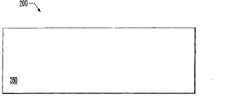
附图2A至2F显示了本发明的另一个实施例中的选定步骤,即构建一个用于检测生物分子的有机场效应晶体管200的方法。晶体管200的类似特征使用在附图1中所示的近似的参数来描述。如图2A所示,该方法包括提供一种常规的基质280,该基质包含,例如硅片。Figures 2A to 2F show selected steps in another embodiment of the present invention, a method of constructing an organic
如图2B所示,闸门结构285形成于基质280之上,适宜的具传导性的闸门物质包括金属(例如金)或具传导性的多聚体(例如掺杂质的多聚噻吩)。闸门结构285可以用常规技术来沉积,例如化学气相沉积,物理喷涂沉积或电子束气化处理等方法。另外,用于形成闸门结构285的材料还可包括基质的一部分,例如掺杂常规的掺杂剂(例如硼或磷)的硅,从而使基质280的一部分具传导性。下面进一步讨论,当需要得到多个有机场效应晶体管200时,用标准的光蚀刻技术构造闸门材料以形成闸门阵列,该阵列在图中未单独显示。As shown in FIG. 2B , a
如图2C所示,绝缘层240沉积在闸门结构285之上,适宜的绝缘层140的材料包括绝缘材料,例如二氧化硅或聚酰亚胺,绝缘层140使用常规的方法,例如使用四乙基正硅酸盐的化学气相沉积,或在含杂质的硅闸门上进行热沉积来得到。绝缘层140在单个的闸门被构造后按照常规的方式构造。As shown in FIG. 2C, an insulating
如图2D所示,流入电极(270)和流出电极(275)位于绝缘层240之上,流入电极(270)和流出电极(275)包含金属或与应用于闸门结构285的多聚体类似的多聚体,应用于形成闸门结构的类似方法也可以应用于沉积流入电极和流出电极的材料,然后应用构造工艺去形成流入电极和流出电极区域(270和275),以容纳一个或更多的装置200的通道区域210。As shown in FIG. 2D, the inflow electrode (270) and the outflow electrode (275) are located on the insulating
如图2E所示,晶体管通道210的形成包括在流入电极和流出电极(270和275)之间形成含有机分子(220)的半导体膜215,优选的,含有机分子220的半导体膜215形成在基质280之上,更优选的,形成在绝缘层240之上。当有机分子220为寡聚体时,膜优选通过真空升华的方法得到。通常,真空升华以本领域技术人员所熟知的常规方法在压力1×10⁻⁴-1×10⁻⁶托之间操作。由于真空升华使得操作相对简化因而是优选的,举例来说,它不需要附加的步骤使有机分子220功能化,从而使其在适于旋转涂层的溶液中更易溶。As shown in FIG. 2E, the formation of the
如果选定的有机分子220不适于进行真空升华,并且它至少微溶于有机溶剂,例如甲苯氯仿或二甲苯,那么可以使用其他常规方法,例如溶液旋转涂层,气化沉积法或印记法。在某些情况下,可以通过功能化有机分子220,例如多聚噻吩,来提高它在用于旋转涂层的溶剂中的溶解性。这样的功能化的例子是区域规则排列(regio-regular)的多聚3-己基噻吩。If the selected
如图2F所示,通道210的形成包括将探针分子225偶联至半导体膜215的外表面230上,这样使得半导体膜215的内部基本上没有探针分子225。探针分子225和膜215上的有机分子220的偶联通过使用本领域普通技术人员所熟知的常规技术得以实现。这样的方法见“Korri-Youssoufi,H.,et al.J.Am.Chem.Soc.119:7388-89(1997)”,以及“Katz,H.E.,et al.Chem.Mater.10:633-38(1998)”的描述。这些文献在此处整体引入作为参考。As shown in FIG. 2F , the formation of the
举例来说,功能基团(264)可附着在有机分子(220)的末端255以促进与探针分子225的偶联。在某些例子中,需要在形成膜215的过程中保护附着在有机分子(220)上的功能基团(264)。然后功能基团264再进行去保护,以暴露与探针分子225反应的功能基团,类似的考虑也适用于功能基团262与探针分子225的结合以及位于功能基团之间的任选的间隔基团(266)的导入。For example, a functional group ( 264 ) can be attached to the
举例来说,有机分子220为六噻吩,探针分子225为单链寡聚体DNA或RNA,探针DNA或RNA(225)可以通过附着在膜215的有机分子220的末端255上的氨基功能基团(262)与探针DNA或RNA(225)的酸性基团发生反应形成酰胺键来偶联至膜215上。另外,附着在有机分子220末端(255)的巯基功能基团(264)可以与位于探针分子(225)上的巯基反应形成二硫键,从而使得探针分子225偶联至膜215上。如上所述,巯基功能基团(264)可以在形成膜215的过程中经乙酰化作用后形成巯基酯(例如形成CH3-CO-S-R,其中R为有机分子240或如上讨论过的偶联在有机分子240上的连接基团260)从而得到保护,然后通过暴露于氢氧化铵而进行去保护。For example, the
在一些实施方案中,探针分子225和半导体膜215之间的偶联作用优选在溶剂中进行,其中该溶剂不溶解膜215的有机分子220,适宜的溶剂包括水或有机溶剂(例如乙醇和乙氰)。使用这样的有机溶剂有助于防止在探针分子225和膜外表面230偶联时探针分子225扩散进入膜215内部。在某些情况下,有机分子优选是寡聚体,例如六噻吩,因为与多聚体(例如多聚噻吩)相比,寡聚体在此类有机溶剂中的溶解性要小。In some embodiments, the coupling between the
如上面所提到的,形成通道210包括将探针分子225偶联于半导体膜的外表面230。在探针分子225和有机分子220偶联之前,通过形成含有机分子220的膜215,可以确保膜215内部基本上没有探针分子225。优选的,探针分子225偶联于位于膜外表面230的有机分子220,更优选的,探针分子225偶联至与膜外表面230最接近的有机分子的末端。下面要进一步讨论,在某些优选的实施例中,具有多个晶体管200,每个都具有偶联至与其相连的通道210上的不同的探针分子225,这样就形成了位于单个基质280上的包括不同的场效晶体管200的阵列。在这样的例子中,可以应用喷墨打印技术或微流体装置来将不同的探针分子225沉积于位于阵列中的通道210之上。As mentioned above, forming the
图3所示是本发明的又一个实施例,用于检测生物靶分子的生物传感器系统(300)。该系统包括生物传感器装置(310),该装置又包括许多有机场效应晶体管(320),如上所述,晶体管具有一个通道(325),该通道包括半导体膜和偶联至膜外表面的探针分子。在某些实施例中,晶体管(320)具有位于每一通道(325)内的不同类型的探针分子,该探针分子有结合不同类型的靶分子(330)的能力。以上所讨论的实施例中的任何的晶体管(320)和靶分子(335)都可包括在系统(300)之中。Fig. 3 shows another embodiment of the present invention, a biosensor system (300) for detecting biological target molecules. The system includes a biosensor device (310) which in turn includes a number of organic field effect transistors (320) having a channel (325) including a semiconducting membrane and probes coupled to the outer surface of the membrane as described above molecular. In certain embodiments, the transistor (320) has within each channel (325) a different type of probe molecule capable of binding a different type of target molecule (330). Any of the transistors (320) and target molecules (335) of the embodiments discussed above may be included in the system (300).
该系统进一步包括一个可以使生物传感器装置310与样品(330)接触的检测系统(340),该检测系统340包括本领域的技术人员所熟知的手动或机器操纵的流体工作站,该工作站具有多个打印头,可以将探针分子和样品加入生物传感器的晶体管中。优选的,如图3所示,该检测系统(340)包括一个偶联至晶体管(320)上的微流体网络(345),该网络可以使晶体管的通道与晶体管的其它组分(例如晶体管的流入电极和流出电极(350和355))之间发生电隔离。在其它优选的实施例中,该微流体网络(345)具有导管(360),该导管可以将样品导入生物传感器装置中彼此不相连的晶体管320中,以便进行同时或并行的样品分析。这样的网络可以含有高弹体硅树脂(例如聚二甲基硅氧烷),并可按照本领域技术人员所熟知的方法得到(见如Thorsen et al.Science 298:580-584(2000),在此整体引入作为参考。)。The system further includes a detection system (340) capable of contacting the
尽管本发明进行了详细描述,对于本领域的普通技术人员来说,应当可以理解在本发明范围之内可以进行各种变化,替代和改变,而不脱离本发明的范围。Although the present invention has been described in detail, those skilled in the art should understand that they can make various changes, substitutions and alterations within the scope of the invention without departing from the scope of the invention.
本申请还公开了以下内容:The application also discloses the following:
1.一种用于检测生物靶分子的有机场效应晶体管,该晶体管包括:1. An organic field effect transistor for detecting biological target molecules, the transistor comprising:
具有半导体膜的晶体管通道,该半导体膜包含有机分子和偶联至所述半导体膜外表面的探针分子,所述膜的内部基本上不存在所述探针分子。A transistor channel having a semiconductor film comprising organic molecules and probe molecules coupled to an outer surface of the semiconductor film, the interior of the film being substantially free of the probe molecules.
2.项目1所述的晶体管,其中所述有机分子具有共轭π键。2. The transistor according to item 1, wherein the organic molecule has a conjugated π bond.
3.项目1所述的晶体管,其中所述半导体膜包含单层的所述有机分子,其中所述有机分子的一端偶联至闸门绝缘体之上,该闸门绝缘体位于所述半导体膜之下。3. The transistor of item 1, wherein the semiconductor film comprises a single layer of the organic molecule, wherein one end of the organic molecule is coupled to a gate insulator that is located below the semiconductor film.
4.项目1所述的晶体管,其中所述半导体膜进一步包括连接分子,该连接分子偶联至所述外表面的所述有机分子并且偶联至所述探针分子之一。4. The transistor of item 1, wherein the semiconductor film further includes a linker molecule coupled to the organic molecule of the outer surface and coupled to one of the probe molecules.
5.项目1所述的晶体管,其中所述晶体管通道为一活性通道,并且其中所述探针分子可以结合靶分子并且化学键合至所述外表面。5. The transistor of item 1, wherein the transistor channel is an active channel, and wherein the probe molecule can bind a target molecule and chemically bond to the outer surface.
6.构建用于检测生物靶分子的有机场效应晶体管的方法,包括:6. A method for constructing an organic field effect transistor for detecting biological target molecules, comprising:
形成晶体管通道,其中包括:Forms the transistor channel, which includes:
在流入电极和流出电极之间形成包含有机分子的半导体膜;以及forming a semiconductor film containing organic molecules between the inflow electrode and the outflow electrode; and
将探针分子与所述半导体膜的外表面偶联,所述半导体膜的内部基本上不存在所述探针分子。Probe molecules are coupled to the outer surface of the semiconductor film, the interior of the semiconductor film being substantially free of the probe molecules.
7.项目6所述的方法,其中所述有机分子进一步包括可以促进所述偶联反应的功能基团。7. The method of item 6, wherein the organic molecule further comprises a functional group that can facilitate the coupling reaction.
8.项目6所述的方法,其中所述探针分子偶联至最接近于所述膜的所述外表面的所述有机分子的末端。8. The method of item 6, wherein the probe molecule is coupled to the end of the organic molecule closest to the outer surface of the membrane.
9.项目6所述的方法,其中靶分子与所述探针分子的结合导致了所述通道的传导性或迁移率的改变。9. The method of item 6, wherein binding of a target molecule to said probe molecule results in a change in the conductivity or mobility of said channel.
10.一种用于检测生物靶分子的生物传感器系统,该系统包括:10. A biosensor system for detecting biological target molecules, the system comprising:
生物传感器装置,该装置包括:A biosensor device comprising:
一个或多个有机场效应晶体管,每一个所述晶体管都包括通道,该通道包括:One or more organic field effect transistors, each of said transistors comprising a channel comprising:
含有机分子的半导体膜;以及semiconductor films containing organic molecules; and
偶联至所述半导体膜外表面上的能够与靶分子结合的探针分子,所述半导体膜的内部基本上不存在所述探针分子;coupled to a probe molecule capable of binding to a target molecule on the outer surface of the semiconductor film, the probe molecule being substantially absent from the interior of the semiconductor film;
能包含所述靶分子的样品;以及a sample capable of comprising said target molecule; and
让所述生物传感器装置与所述样品接触的检测系统。A detection system contacts the biosensor device with the sample.
Claims (12)
Translated fromChineseApplications Claiming Priority (2)
| Application Number | Priority Date | Filing Date | Title |
|---|---|---|---|
| US10/405,398 | 2003-04-02 | ||
| US10/405,398US7189987B2 (en) | 2003-04-02 | 2003-04-02 | Electrical detection of selected species |
Related Parent Applications (1)
| Application Number | Title | Priority Date | Filing Date |
|---|---|---|---|
| CNA2004100326708ADivisionCN1540328A (en) | 2003-04-02 | 2004-04-01 | Electrical detection of selected substances |
Publications (2)
| Publication Number | Publication Date |
|---|---|
| CN101487815A CN101487815A (en) | 2009-07-22 |
| CN101487815Btrue CN101487815B (en) | 2012-05-09 |
Family
ID=32850614
Family Applications (2)
| Application Number | Title | Priority Date | Filing Date |
|---|---|---|---|
| CN2008101779775AExpired - Fee RelatedCN101487815B (en) | 2003-04-02 | 2004-04-01 | Electrical detection of selected species |
| CNA2004100326708APendingCN1540328A (en) | 2003-04-02 | 2004-04-01 | Electrical detection of selected substances |
Family Applications After (1)
| Application Number | Title | Priority Date | Filing Date |
|---|---|---|---|
| CNA2004100326708APendingCN1540328A (en) | 2003-04-02 | 2004-04-01 | Electrical detection of selected substances |
Country Status (5)
| Country | Link |
|---|---|
| US (2) | US7189987B2 (en) |
| EP (1) | EP1464953B1 (en) |
| JP (1) | JP4625266B2 (en) |
| KR (2) | KR101129503B1 (en) |
| CN (2) | CN101487815B (en) |
Families Citing this family (46)
| Publication number | Priority date | Publication date | Assignee | Title |
|---|---|---|---|---|
| US20080258179A1 (en)* | 2004-06-21 | 2008-10-23 | William Marsh Rice University | Hybrid molecular electronic device for switching, memory, and sensor applications, and method of fabricating same |
| US8362559B2 (en)* | 2002-02-01 | 2013-01-29 | William Marsh Rice University | Hybrid molecular electronic devices containing molecule-functionalized surfaces for switching, memory, and sensor applications and methods for fabricating same |
| US7189987B2 (en)* | 2003-04-02 | 2007-03-13 | Lucent Technologies Inc. | Electrical detection of selected species |
| US7291496B2 (en) | 2003-05-22 | 2007-11-06 | University Of Hawaii | Ultrasensitive biochemical sensor |
| JP4194436B2 (en)* | 2003-07-14 | 2008-12-10 | キヤノン株式会社 | Field effect organic transistor |
| US7317216B2 (en)* | 2003-10-31 | 2008-01-08 | University Of Hawaii | Ultrasensitive biochemical sensing platform |
| US8536661B1 (en) | 2004-06-25 | 2013-09-17 | University Of Hawaii | Biosensor chip sensor protection methods |
| KR100682918B1 (en)* | 2005-01-20 | 2007-02-15 | 삼성전자주식회사 | FET type biosensor with surface modification |
| JP2006242900A (en)* | 2005-03-07 | 2006-09-14 | Mitsubishi Chemicals Corp | Sensor unit, reaction field cell unit and analyzer |
| KR100773550B1 (en)* | 2006-04-03 | 2007-11-07 | 삼성전자주식회사 | Method of detecting biomolecules using field effect transistor without fixing biomolecules |
| CN100555702C (en)* | 2006-04-29 | 2009-10-28 | 中国科学院长春应用化学研究所 | Preparation method and application of organic semiconductor crystal thin film and weakly oriented epitaxial growth |
| BRPI0712809A2 (en)* | 2006-05-29 | 2012-10-23 | Koninkl Philips Electronics Nv | field effect transistor, sensor system, and, use of a sensor system |
| US7863603B1 (en)* | 2006-07-24 | 2011-01-04 | The Board Of Trustees Of The Leland Stanford Junior University | Cross-linked organic thin-film dielectrics |
| KR101340995B1 (en)* | 2006-12-28 | 2013-12-13 | 엘지디스플레이 주식회사 | Thin film transistor using liquid crystal display device |
| KR100845004B1 (en)* | 2007-04-30 | 2008-07-09 | 삼성전자주식회사 | Method of forming a metal film pattern having a nano gap and a method of manufacturing a molecule size device using the same |
| US8384409B2 (en)* | 2007-05-03 | 2013-02-26 | The Regents Of The University Of California | Ultra-thin organic TFT chemical sensor, making thereof, and sensing method |
| EP2174122A2 (en)* | 2007-06-08 | 2010-04-14 | Bharath R Takulapalli | Nano structured field effect sensor and methods of forming and using same |
| JP2010530063A (en)* | 2007-06-08 | 2010-09-02 | バラス アール. タクラパリ, | Nanostructured field effect sensor and method of forming and using the same |
| US8198658B2 (en)* | 2007-06-13 | 2012-06-12 | Samsung Electronics Co., Ltd. | Device and method for detecting biomolecules using adsorptive medium and field effect transistor |
| WO2009017631A2 (en) | 2007-07-26 | 2009-02-05 | The Regents Of The University Of California | Peroxide chemical sensor and sensing method |
| KR101465961B1 (en)* | 2007-10-09 | 2014-12-01 | 삼성전자주식회사 | Gene detection method and apparatus |
| KR100906144B1 (en)* | 2007-12-05 | 2009-07-07 | 한국전자통신연구원 | Detection element and manufacturing method of the detection element |
| FR2938703B1 (en)* | 2008-11-20 | 2011-04-22 | Commissariat Energie Atomique | METHOD FOR PRODUCING A CHIP FOR DETECTING BIOLOGICAL ELEMENTS |
| KR101136881B1 (en)* | 2008-12-03 | 2012-04-20 | 한국전자통신연구원 | Biosensor Having Transistor Structure and Method for Fabricating the Same |
| JP4843077B2 (en)* | 2008-12-03 | 2011-12-21 | 韓國電子通信研究院 | Biosensor with transistor structure and manufacturing method thereof |
| KR101050695B1 (en)* | 2008-12-15 | 2011-07-20 | 한국전자통신연구원 | Manufacturing method of transistor for biosensor |
| GB2469331A (en) | 2009-04-09 | 2010-10-13 | Tech Universit T Graz | OFET-based sensor with organic gate dielectric for detecting an analyte |
| KR101022927B1 (en) | 2009-05-25 | 2011-03-16 | 삼성전기주식회사 | Biochip and its manufacturing method using aptamer |
| EP2366994A1 (en)* | 2010-03-18 | 2011-09-21 | Wolfgang Knoll | Biosensor on thin-film transistors |
| WO2012050873A2 (en)* | 2010-09-29 | 2012-04-19 | The Board Of Regents Of The University Of Texas System | Fin-fet biosensor with improved sensitivity and specificity |
| CA2835194A1 (en) | 2011-05-05 | 2012-11-08 | Daktari Diagnostics, Inc. | Conductive patterns and methods for making conductive patterns |
| WO2012168932A1 (en)* | 2011-06-06 | 2012-12-13 | Yeda Research And Development Co. Ltd | Protein detector based on molecular controlled semiconductor resistor |
| US8877022B2 (en)* | 2011-06-21 | 2014-11-04 | National Taiwan University | Biosensor |
| RU2546018C2 (en)* | 2011-06-21 | 2015-04-10 | Нэйшнл Тайвань Юниверсити | Biosensor |
| EP2836828B1 (en) | 2012-04-09 | 2022-12-14 | Takulapalli, Bharath | Field effect transistor, device including the transistor, and methods of forming and using same |
| EP2975391A1 (en)* | 2014-07-17 | 2016-01-20 | Peptisyntha Sa | Chemosensor, its method of manufacture, and a method for the selective detection of analytes |
| DE102014215492A1 (en)* | 2014-08-06 | 2016-02-11 | Robert Bosch Gmbh | Sensor for detecting at least one chemical species and method for its production |
| WO2016047340A1 (en)* | 2014-09-24 | 2016-03-31 | 富士フイルム株式会社 | Gas sensor and organic transistor |
| US10991894B2 (en)* | 2015-03-19 | 2021-04-27 | Foundation Of Soongsil University-Industry Cooperation | Compound of organic semiconductor and organic semiconductor device using the same |
| CN105136893B (en)* | 2015-06-24 | 2017-11-07 | 中国科学院宁波材料技术与工程研究所 | A kind of thin film transistor (TFT) biology sensor and preparation method thereof |
| CN109313157B (en) | 2016-04-19 | 2024-03-29 | 巴拉什·塔库拉帕里 | Nanopore sensor, structures and devices including the sensor, and methods of forming and using the same |
| US20190285576A1 (en)* | 2016-10-24 | 2019-09-19 | Toray Industries, Inc. | Semiconductor sensor, method for producing the same, and combined sensor |
| KR102300186B1 (en)* | 2018-08-30 | 2021-09-10 | 서울대학교산학협력단 | Two electrode system and biosensor including the same |
| WO2020046065A1 (en)* | 2018-08-30 | 2020-03-05 | 서울대학교 산학협력단 | Two electrode system and biosensor comprising same |
| US10968098B2 (en)* | 2018-10-02 | 2021-04-06 | International Business Machines Corporation | Selective functionalization of sensing surface with nanoscale spatial resolution |
| US11143584B2 (en) | 2018-10-02 | 2021-10-12 | International Business Machines Corporation | Selective functionalization of sensing surface |
Family Cites Families (18)
| Publication number | Priority date | Publication date | Assignee | Title |
|---|---|---|---|---|
| DE3688489T2 (en)* | 1985-08-29 | 1993-09-16 | Matsushita Electric Ind Co Ltd | SENSORS USING A FIELD EFFECT TRANSISTOR AND THEIR PRODUCTION METHOD. |
| US5154808A (en)* | 1987-06-26 | 1992-10-13 | Fuji Photo Film Co., Ltd. | Functional organic thin film and process for producing the same |
| US4886625A (en)* | 1987-10-29 | 1989-12-12 | Miles Inc. | Functionalized conducting polymers and their use in diagnostic devices |
| US5491097A (en)* | 1989-06-15 | 1996-02-13 | Biocircuits Corporation | Analyte detection with multilayered bioelectronic conductivity sensors |
| JPH05312746A (en) | 1992-05-06 | 1993-11-22 | Mitsubishi Electric Corp | Bad-smell sensor |
| FR2720832A1 (en)* | 1994-04-22 | 1995-12-08 | Francis Garnier | Electroactive electrodes and membranes based on bioactive peptides, for the recognition, extraction or release of biologically active species. |
| WO1997027316A1 (en) | 1996-01-26 | 1997-07-31 | The Regents Of The University Of California | Polymeric film, assay and method for direct colorimetric detection of analytes |
| US6203981B1 (en)* | 1996-04-17 | 2001-03-20 | Motorola, Inc. | Transistor-based molecular detection apparatus and method |
| JPH10260156A (en) | 1997-03-18 | 1998-09-29 | Hitachi Ltd | sensor |
| JP2000033712A (en)* | 1997-09-30 | 2000-02-02 | Seiko Epson Corp | Microsensor device manufacturing method and liquid function evaluation method using the same |
| EP1085319B1 (en) | 1999-09-13 | 2005-06-01 | Interuniversitair Micro-Elektronica Centrum Vzw | A device for detecting an analyte in a sample based on organic materials |
| JP4587539B2 (en)* | 1999-09-13 | 2010-11-24 | アイメック | Apparatus for detecting analytes in samples based on organic materials |
| DE19963381A1 (en)* | 1999-12-28 | 2001-07-12 | Aventis Cropscience Gmbh | Surfactant / solvent systems |
| JP2002017352A (en)* | 2000-04-28 | 2002-01-22 | Fuji Photo Film Co Ltd | Tool for detecting nucleic acid specimen and method for electrochemical detection |
| US6545758B1 (en)* | 2000-08-17 | 2003-04-08 | Perry Sandstrom | Microarray detector and synthesizer |
| US20020167003A1 (en)* | 2001-04-18 | 2002-11-14 | Campbell Ian H. | Chemical and biological sensor using organic self-assembled transitors |
| US20020171125A1 (en)* | 2001-05-17 | 2002-11-21 | Zhenan Bao | Organic semiconductor devices with short channels |
| US7189987B2 (en) | 2003-04-02 | 2007-03-13 | Lucent Technologies Inc. | Electrical detection of selected species |
- 2003
- 2003-04-02USUS10/405,398patent/US7189987B2/ennot_activeExpired - Lifetime
- 2004
- 2004-03-23EPEP04251670.8Apatent/EP1464953B1/ennot_activeExpired - Lifetime
- 2004-03-25KRKR1020040020459Apatent/KR101129503B1/ennot_activeExpired - Fee Related
- 2004-04-01CNCN2008101779775Apatent/CN101487815B/ennot_activeExpired - Fee Related
- 2004-04-01CNCNA2004100326708Apatent/CN1540328A/enactivePending
- 2004-04-02JPJP2004109679Apatent/JP4625266B2/ennot_activeExpired - Fee Related
- 2006
- 2006-05-31USUS11/421,125patent/US7534646B2/ennot_activeExpired - Fee Related
- 2012
- 2012-02-01KRKR1020120010509Apatent/KR101235860B1/ennot_activeExpired - Fee Related
Also Published As
| Publication number | Publication date |
|---|---|
| US20060243969A1 (en) | 2006-11-02 |
| KR20120031967A (en) | 2012-04-04 |
| CN1540328A (en) | 2004-10-27 |
| KR101235860B1 (en) | 2013-02-20 |
| US20040195563A1 (en) | 2004-10-07 |
| US7189987B2 (en) | 2007-03-13 |
| US7534646B2 (en) | 2009-05-19 |
| CN101487815A (en) | 2009-07-22 |
| JP2004309483A (en) | 2004-11-04 |
| KR20040086196A (en) | 2004-10-08 |
| JP4625266B2 (en) | 2011-02-02 |
| EP1464953B1 (en) | 2015-09-23 |
| KR101129503B1 (en) | 2012-03-30 |
| EP1464953A1 (en) | 2004-10-06 |
Similar Documents
| Publication | Publication Date | Title |
|---|---|---|
| CN101487815B (en) | Electrical detection of selected species | |
| Patolsky et al. | Nanowire nanosensors | |
| Lud et al. | Field Effect of Screened Charges: Electrical Detection of Peptides and Proteins by a Thin‐Film Resistor | |
| US8017938B2 (en) | Apparatus for microarray binding sensors having biological probe materials using carbon nanotube transistors | |
| US9575029B2 (en) | Method to realize electronic field-effect transistor sensors | |
| US20070207471A1 (en) | Semiconductor DNA sensing device and DNA sensing method | |
| Duan et al. | Functionalized polyelectrolytes assembling on nano‐BioFETs for biosensing applications | |
| US7635423B2 (en) | Redox potential mediated, heterogeneous, carbon nanotube biosensing | |
| CN102016570A (en) | Methods of Using and Building Nanosensor Platforms | |
| EP1504263A1 (en) | Polyelectrolyte complex (e.g.zwitterionic polythiophenes) with a receptor (e.g. polynucleotide, antibody etc.) for biosensor applications | |
| WO2007114140A1 (en) | Carbon nanotube electric field effect transistor and process for producing the same | |
| Li et al. | Recent advances in immobilization strategies for biomolecules in sensors using organic field-effect transistors | |
| TW201630807A (en) | Carbon nanotube composite, semiconductor element and production method therefor, and sensor using same | |
| US20060194263A1 (en) | Small molecule mediated, heterogeneous, carbon nanotube biosensing | |
| JP4482856B2 (en) | Method for detecting target substance in sample, sensor substrate, and detection kit | |
| Coffinier et al. | Surface modification of semiconducting silicon nanowires for biosensing applications | |
| KR101085879B1 (en) | Biosensor using silicon nanowires, manufacturing method of biosensor using silicon nanowires and specific cell detection method using the biosensor | |
| Murugan et al. | Comparative Study of Surface Activation Steps for Thermally Grown Oxide Interface and Optimal Silanization | |
| KR101136881B1 (en) | Biosensor Having Transistor Structure and Method for Fabricating the Same | |
| Javed et al. | Advances in DNA Sensing Using BioFETs | |
| Lee | Self-Assembled Nanotube/Nanoparticle Biosensors |
Legal Events
| Date | Code | Title | Description |
|---|---|---|---|
| C06 | Publication | ||
| PB01 | Publication | ||
| C10 | Entry into substantive examination | ||
| SE01 | Entry into force of request for substantive examination | ||
| C14 | Grant of patent or utility model | ||
| GR01 | Patent grant | ||
| CF01 | Termination of patent right due to non-payment of annual fee | Granted publication date:20120509 Termination date:20200401 | |
| CF01 | Termination of patent right due to non-payment of annual fee |