CN101480743A - Electroprocessing profile control - Google Patents
Electroprocessing profile controlDownload PDFInfo
- Publication number
- CN101480743A CN101480743ACNA2008101757013ACN200810175701ACN101480743ACN 101480743 ACN101480743 ACN 101480743ACN A2008101757013 ACNA2008101757013 ACN A2008101757013ACN 200810175701 ACN200810175701 ACN 200810175701ACN 101480743 ACN101480743 ACN 101480743A
- Authority
- CN
- China
- Prior art keywords
- substrate
- electrode
- bias
- electrolyte
- grinding
- Prior art date
- Legal status (The legal status is an assumption and is not a legal conclusion. Google has not performed a legal analysis and makes no representation as to the accuracy of the status listed.)
- Pending
Links
Images


Classifications
- B—PERFORMING OPERATIONS; TRANSPORTING
- B23—MACHINE TOOLS; METAL-WORKING NOT OTHERWISE PROVIDED FOR
- B23H—WORKING OF METAL BY THE ACTION OF A HIGH CONCENTRATION OF ELECTRIC CURRENT ON A WORKPIECE USING AN ELECTRODE WHICH TAKES THE PLACE OF A TOOL; SUCH WORKING COMBINED WITH OTHER FORMS OF WORKING OF METAL
- B23H5/00—Combined machining
- B23H5/06—Electrochemical machining combined with mechanical working, e.g. grinding or honing
- B23H5/08—Electrolytic grinding
- B—PERFORMING OPERATIONS; TRANSPORTING
- B24—GRINDING; POLISHING
- B24B—MACHINES, DEVICES, OR PROCESSES FOR GRINDING OR POLISHING; DRESSING OR CONDITIONING OF ABRADING SURFACES; FEEDING OF GRINDING, POLISHING, OR LAPPING AGENTS
- B24B37/00—Lapping machines or devices; Accessories
- B24B37/04—Lapping machines or devices; Accessories designed for working plane surfaces
- B24B37/042—Lapping machines or devices; Accessories designed for working plane surfaces operating processes therefor
- C—CHEMISTRY; METALLURGY
- C25—ELECTROLYTIC OR ELECTROPHORETIC PROCESSES; APPARATUS THEREFOR
- C25F—PROCESSES FOR THE ELECTROLYTIC REMOVAL OF MATERIALS FROM OBJECTS; APPARATUS THEREFOR
- C25F7/00—Constructional parts, or assemblies thereof, of cells for electrolytic removal of material from objects; Servicing or operating
- H—ELECTRICITY
- H01—ELECTRIC ELEMENTS
- H01L—SEMICONDUCTOR DEVICES NOT COVERED BY CLASS H10
- H01L21/00—Processes or apparatus adapted for the manufacture or treatment of semiconductor or solid state devices or of parts thereof
- H01L21/02—Manufacture or treatment of semiconductor devices or of parts thereof
- H01L21/04—Manufacture or treatment of semiconductor devices or of parts thereof the devices having potential barriers, e.g. a PN junction, depletion layer or carrier concentration layer
- H01L21/18—Manufacture or treatment of semiconductor devices or of parts thereof the devices having potential barriers, e.g. a PN junction, depletion layer or carrier concentration layer the devices having semiconductor bodies comprising elements of Group IV of the Periodic Table or AIIIBV compounds with or without impurities, e.g. doping materials
- H01L21/30—Treatment of semiconductor bodies using processes or apparatus not provided for in groups H01L21/20 - H01L21/26
- H01L21/302—Treatment of semiconductor bodies using processes or apparatus not provided for in groups H01L21/20 - H01L21/26 to change their surface-physical characteristics or shape, e.g. etching, polishing, cutting
- H01L21/304—Mechanical treatment, e.g. grinding, polishing, cutting
- H—ELECTRICITY
- H01—ELECTRIC ELEMENTS
- H01L—SEMICONDUCTOR DEVICES NOT COVERED BY CLASS H10
- H01L21/00—Processes or apparatus adapted for the manufacture or treatment of semiconductor or solid state devices or of parts thereof
- H01L21/02—Manufacture or treatment of semiconductor devices or of parts thereof
- H01L21/04—Manufacture or treatment of semiconductor devices or of parts thereof the devices having potential barriers, e.g. a PN junction, depletion layer or carrier concentration layer
- H01L21/18—Manufacture or treatment of semiconductor devices or of parts thereof the devices having potential barriers, e.g. a PN junction, depletion layer or carrier concentration layer the devices having semiconductor bodies comprising elements of Group IV of the Periodic Table or AIIIBV compounds with or without impurities, e.g. doping materials
- H01L21/30—Treatment of semiconductor bodies using processes or apparatus not provided for in groups H01L21/20 - H01L21/26
- H01L21/31—Treatment of semiconductor bodies using processes or apparatus not provided for in groups H01L21/20 - H01L21/26 to form insulating layers thereon, e.g. for masking or by using photolithographic techniques; After treatment of these layers; Selection of materials for these layers
- H01L21/3205—Deposition of non-insulating-, e.g. conductive- or resistive-, layers on insulating layers; After-treatment of these layers
- H01L21/321—After treatment
- C—CHEMISTRY; METALLURGY
- C25—ELECTROLYTIC OR ELECTROPHORETIC PROCESSES; APPARATUS THEREFOR
- C25D—PROCESSES FOR THE ELECTROLYTIC OR ELECTROPHORETIC PRODUCTION OF COATINGS; ELECTROFORMING; APPARATUS THEREFOR
- C25D17/00—Constructional parts, or assemblies thereof, of cells for electrolytic coating
- C25D17/10—Electrodes, e.g. composition, counter electrode
Landscapes
- Engineering & Computer Science (AREA)
- Chemical & Material Sciences (AREA)
- Mechanical Engineering (AREA)
- Electrochemistry (AREA)
- Chemical Kinetics & Catalysis (AREA)
- Manufacturing & Machinery (AREA)
- Materials Engineering (AREA)
- Microelectronics & Electronic Packaging (AREA)
- Power Engineering (AREA)
- General Physics & Mathematics (AREA)
- Condensed Matter Physics & Semiconductors (AREA)
- Physics & Mathematics (AREA)
- Computer Hardware Design (AREA)
- Metallurgy (AREA)
- Organic Chemistry (AREA)
- Mechanical Treatment Of Semiconductor (AREA)
- Finish Polishing, Edge Sharpening, And Grinding By Specific Grinding Devices (AREA)
- Electrochromic Elements, Electrophoresis, Or Variable Reflection Or Absorption Elements (AREA)
- Control Of Indicators Other Than Cathode Ray Tubes (AREA)
- Electrical Discharge Machining, Electrochemical Machining, And Combined Machining (AREA)
Abstract
Translated fromChinese
Description
Translated fromChinese本发明是提交于2006年1月24日,申请号为200680002929.1,题为“电处理轮廓控制”的发明专利申请的分案申请。The present invention is a divisional application of the invention patent application entitled "Electrical Processing Contour Control" filed on January 24, 2006 with application number 200680002929.1.
技术领域technical field
本发明的实施例大致上是有关于用于电处理基材的轮廓控制。Embodiments of the present invention generally relate to profile control for electrical processing of substrates.
背景技术Background technique
与传统的化学机械研磨(Chemical Mechanical Polishing,CMP)制程相互比较,电化学机械研磨(Electrochemical Mechanical Polishing,Ecmp)为通过电化学溶解而同时以较少的磨耗来研磨基材,以自基材表面移除导电材料的技术。电化学溶解是通过在一阴极与一基材表面之间施加一偏压以自基材表面移除导电材料进入周围电解质中来执行。该偏压可以经由位于基材上的一导电接触件或一研磨材料而被施加至基材表面,其中该基材被处理于该研磨材料上。研磨制程的一机械部件是通过提供基材与研磨材料之间的相对移动而被执行,其是加强了导电材料自基材的移除。Compared with the traditional Chemical Mechanical Polishing (CMP) process, Electrochemical Mechanical Polishing (Ecmp) is to grind the substrate by electrochemical dissolution while using less abrasion to remove the surface of the substrate Techniques for removing conductive materials. Electrochemical dissolution is performed by applying a bias between a cathode and a substrate surface to remove conductive material from the substrate surface into the surrounding electrolyte. The bias voltage can be applied to the surface of the substrate via a conductive contact on the substrate or an abrasive material on which the substrate is being processed. A mechanical component of the grinding process is performed by providing relative movement between the substrate and the abrasive material, which enhances the removal of conductive material from the substrate.
在一些电处理设备中的轮廓控制一般地已经是通过在横越被处理基材宽度建立数个制程单元或区域而被实施。经由控制个别单元之间的电性偏压或电流流动,可以控制基材上的导电材料的移除或沉积速率。Profile control in some electrical processing equipment has generally been implemented by establishing several process cells or zones across the width of the substrate being processed. By controlling the electrical bias or current flow between individual cells, the rate of removal or deposition of conductive material on the substrate can be controlled.
然而,基材边缘之处理速率的控制具有相当大的挑战。因为与位于基材与电极之间的电解质(其定义出一制程单元)比较,邻近于基材的电解质的电位具有更大(更负值)的电位,因此在基材边缘的电压梯度是高的。高电压梯度在基材边缘造成了更大的电流密度与更快的处理。快速边缘处理一般而言不是所希望发生的,这是因为会造成用于组件制造的可使用基材面积的减少。因此,改善一电处理的轮廓控制而使得接近基材边缘区域具有相当于基材中心的材料移除与沉积速率是所希望的。However, control of the processing rate at the edge of the substrate presents considerable challenges. Because the potential of the electrolyte adjacent to the substrate has a larger (more negative) potential than the electrolyte located between the substrate and the electrodes (which defines a process cell), the voltage gradient at the edge of the substrate is high of. High voltage gradients result in higher current densities and faster processing at the edge of the substrate. Fast edge processing is generally undesirable because of the reduction in usable substrate area for component fabrication. Therefore, it would be desirable to improve the profile control of an electrical process such that regions near the edge of the substrate have material removal and deposition rates comparable to the center of the substrate.
因此,用于电处理的一改善的方法与设备是有其需要的。Accordingly, there is a need for an improved method and apparatus for electrical processing.
发明内容Contents of the invention
本发明提供一种用以电处理一基材的方法与设备。在一实施例中,用以电处理一基材的方法包括有以下步骤:将第一电极施加偏压,以建立介于该第一电极与该基材之间的第一电处理区域;以及将第二电极施加偏压以一极性,其中该第二电极是径向地被设置在基材之外,该极性是相反于施加至该第一电极的该偏压。该第二电极的相反偏压造成了一过渡电压梯度以向外移动,藉此改善了在基材边缘处的电处理控制。The present invention provides a method and apparatus for electrically treating a substrate. In one embodiment, a method for electrically treating a substrate includes the steps of: biasing a first electrode to establish a first electrical treatment region between the first electrode and the substrate; and The second electrode is biased with a polarity opposite to the bias applied to the first electrode, wherein the second electrode is disposed radially outwardly of the substrate. Opposite biasing of the second electrode creates a transition voltage gradient to move outward, thereby improving electrical processing control at the edge of the substrate.
在另一实施例中,用以电处理一基材的方法包括有以下步骤:将一基材接触于一研磨表面且在其之间提供相对移动;经由电解质在数个电极与该基材之间建立一导电路径;将该基材相对于该数个电极施加偏压;以及同时地将该数个电极的至少两个施加偏压以正极性。In another embodiment, a method for electrically treating a substrate includes the steps of: contacting a substrate to an abrasive surface and providing relative movement therebetween; establishing a conductive path therebetween; biasing the substrate relative to the plurality of electrodes; and simultaneously biasing at least two of the plurality of electrodes to a positive polarity.
在又一实施例中,用以电处理一基材的设备包括有一处理层、一研磨头与数个电极。处理层包括有一表面,其中该表面是适用以处理其上的一基材。研磨头用以将一基材固持抵靠该研磨表面。至少一驱动机构是适用以在该处理层与该研磨头之间提供相对移动。该驱动机构在该处理层与该研磨头之间提供一移动范围,其中该移动范围至少部分地定义了在该处理表面上的一处理区域。该数个电极位于该处理层下方,其中至少第一电极被设置在该处理层之外,至少第二电极与第三电极被设置在该第一电极之内,并且至少第四电极被设置在该第二电极之内且具有比该第二与第三电极更大的一宽度。In yet another embodiment, an apparatus for electrically processing a substrate includes a processing layer, an abrasive head, and electrodes. The treatment layer includes a surface, wherein the surface is suitable for treating a substrate thereon. The grinding head is used to hold a substrate against the grinding surface. At least one drive mechanism is adapted to provide relative movement between the processing layer and the grinding head. The drive mechanism provides a range of motion between the processing layer and the grinding head, wherein the range of motion at least partially defines a processing area on the processing surface. The plurality of electrodes are located below the processing layer, wherein at least a first electrode is disposed outside the processing layer, at least a second electrode and a third electrode are disposed within the first electrode, and at least a fourth electrode is disposed within the The second electrode is within and has a width greater than that of the second and third electrodes.
附图说明Description of drawings
本发明的特征、优点与目的可由前述说明与所伴随的图式而更加了解。The features, advantages and objects of the present invention can be better understood from the foregoing description and accompanying drawings.
然而必须注意的是,所伴随图式仅绘示出本发明典型实施例,且因此不应被视为本发明范围的限制,本发明可以包含其它同等有效的实施例。It is to be noted, however, that the accompanying drawings illustrate only typical embodiments of this invention and are therefore not to be considered limiting of its scope, for the invention may include other equally effective embodiments.
图1为一电化学机械研磨站的一实施例的部分截面图;1 is a partial cross-sectional view of an embodiment of an electrochemical mechanical polishing station;
图1A-1B为一导电固持环的替代性实施例的截面图;1A-1B are cross-sectional views of an alternative embodiment of a conductive retaining ring;
图2A-2B为图1的研磨站实施例于不同操作模式的部分截面图;2A-2B are partial cross-sectional views of the embodiment of the grinding station of FIG. 1 in different modes of operation;
图3A-3D绘示出一研磨垫组件的电极的不同实施例;3A-3D illustrate different embodiments of electrodes of a polishing pad assembly;
图4为一研磨垫组件的电极的实施例的仰视图,其中该研磨垫组件具有插入于其中的一基材;4 is a bottom view of an embodiment of an electrode of a polishing pad assembly having a substrate inserted therein;
图5是为一图,其绘示出图4的每一电极区段对于自横越基材半径在不同位置处所移除的导电材料的贡献百分比;5 is a graph plotting the percentage contribution of each electrode segment of FIG. 4 to the conductive material removed at different locations across the radius of the substrate;
图6为用以在一Ecmp制程中控制研磨轮廓的方法的实施例的流程图;6 is a flowchart of an embodiment of a method for controlling grinding profile in an Ecmp process;
图7为一图,其绘示出使用图6的方法来维持自基材边缘向外的一过渡电压梯度的效应;Figure 7 is a graph illustrating the effect of using the method of Figure 6 to maintain a transitional voltage gradient outward from the edge of the substrate;
图8为一基材的部分平面图,其绘示出图6的方法如何在处理期间减缓边缘排除在外的成长;以及8 is a partial plan view of a substrate illustrating how the method of FIG. 6 slows edge-excluded growth during processing; and
图9绘示出一研磨垫组件的另一实施例。FIG. 9 illustrates another embodiment of a polishing pad assembly.
为了有助于了解,如果可以的话,本文对于图式中普遍的相同构件是使用了相同的组件代表符号。In order to facilitate understanding, if possible, this text uses the same component representative symbols for the same components that are common in the drawings.
主要组件符号说明Explanation of main component symbols
100 Ecmp站100 Ecmp station
102 驱动系统102 drive system
104 研磨表面104 grinding surface
106 研磨垫组件106 Polishing Pad Assembly
108 孔洞108 holes
110 第一部分110
112 第二部分112 Part Two
114 凹陷部114 depression
116 底部表面116 bottom surface
118 研磨头组件118 grinding head assembly
120 基材120 base material
122 研磨头122 grinding head
124 壳体124 Shell
126 固持环126 retaining ring
130 基座130 base
134 接触构件134 contact member
138 容室138 containment room
142 平台组件142 Platform Components
148 下平板148 down plate
150 上平板150 upper plate
152 顶部表面152 top surface
154 轴承154 bearing
156 出口156 exits
158 支撑件158 supports
160 马达160 motor
164 机械手臂164 robotic arm
170 电解质源170 Electrolyte source
202 非导电表面202 Non-conductive surface
204 导电表面204 conductive surface
208 通道208 channels
210A-210F 区段
211 次垫211 pads
212 上层212 upper floor
218 通道218 channels
220 开孔220 opening
250 包含区域250 inclusive area
252 过渡区域252 Transition area
254 自由区域254 free zone
280 输出终端280 output terminal
302A-302D 垫组件302A-302D Pad Assembly
304 轴304 axis
402 虚线402 dotted line
404 研磨区域404 grinding area
410A-410B 宽度410A-410B Width
500 图500 graphs
502 贡献百分比502 Contribution Percentage
504 径向位置504 radial position
510A-510F 曲线510A-510F curve
600 方法600 methods
602 设置步骤602 Setup steps
604 电解质提供步骤604 Electrolyte provision step
606 施加偏压步骤606 Bias application step
608 过渡维持向外步骤608 Transition Sustained Outward Step
610 终点步骤610 Terminal step
612 过研磨步骤612 Over grinding step
700 图700 graphs
702 x轴702 x-axis
704 y轴704 y-axis
706 曲线706 curve
710 曲线710 curve
714 曲线714 curve
800 基材800 base material
802 外周围802 Outer Perimeter
804 线804 line
806 线806 lines
808 线808 lines
810 线810 lines
812 空白区域812 blank space
900 垫组件900 pad assembly
902 导电表面902 conductive surface
904 次垫904 pads
906 电极906 electrodes
具体实施方式Detailed ways
图1绘示一Ecmp站100的截面图,其是适用以加强自一基材的材料的均匀移除与/或沉积。Ecmp站100包括有一研磨头组件118,其是适用以抓持一基材120而抵靠一平台组件142。在其之间是提供有相对移动以研磨基材120。该相对移动可以为旋转的、侧向的、或其组合,并且可以通过研磨头组件118与平台组件142的其一或两个而被提供。FIG. 1 shows a cross-sectional view of an
在一实施例中,研磨头组件118被一机械手臂164所支撑住,其中该机械手臂164是通过一支撑件158而耦接至一基座130且延伸于Ecmp站100上方。Ecmp站100可以耦接至基座130或位于邻近于基座130之处。In one embodiment, the grinding
研磨头组件118大致上包括一驱动系统102,该驱动系统102耦接至一研磨头122。驱动系统102通常地提供至少一旋转移动至研磨头122。此外,研磨头122可以朝着平台组件142而被启始,使得固持在研磨头122中的基材120在处理期间可以被设置在抵靠住Ecmp站100的一研磨表面104。固持在研磨头122中的基材120可以推压抵顶研磨表面104于小于约2磅/每平方英寸(psi)的压力,并且在另一实施例中为小于约1psi。The grinding
在一实施例中,研磨头122可以为由美国加州圣大克劳拉市的AppliedMaterials,Inc.所制造的TITAN HEADTM或TITAN PROFILERTM晶圆承载件。一般而言,研磨头122至少包含一壳体124与一固持环126,该固持环126是定义出基材120所被固持于其内的一中心凹陷部。固持环126包围住位于研磨头122内的基材120以避免基材在处理期间自研磨头122下方滑出。亦可以考虑使用其它研磨头。In one embodiment, the grinding
固持环126可以由一导电或介电材料所制成。固持环126可以被接地、电性地被偏压或相对于接地而飘浮。在一实施例中,固持环126是耦接至一电源166。例如,如图1A所绘示者,固持环126可以具有第一部分110与第二部分112。第一部分110位于固持环126的底部上,使得第一部分110面对平台组件142。第一部分110是由一导电材料所制成且耦接至电源166。第二部分112可以为一介电材料、导电材料,或是与第一部分被制造而为单一部件的构件。在图1B所绘示的另一实施例中,固持环126的第二部分112包括形成在底部表面116中的一凹陷部114。第一部分110位于凹陷部114中而使得第一部分的底部表面自底部表面116凹陷,而使包含有第一部分110的导电材料在处理期间不接触于研磨表面104。The retaining
平台组件142是通过一轴承154被支撑在基座130上以促进平台组件142相对于基座130的旋转。平台组件142典型地是耦接至一马达,该马达是提供旋转移动至平台组件142。The
平台组件142具有一上平板150与一下平板148。上平板150可以由一坚硬材料(例如金属或坚硬塑料)所制成,并且在一实施例中是由一介电材料所制成或被涂覆以介电材料,该介电材料是例如氯化聚氯乙烯(CPVC)。上平板150可以具有一圆形、矩形或其它具有一平坦上表面的几何形式。上平板150的一顶部表面136是支撑住一研磨垫组件106,其中该研磨垫组件106包括有其上的研磨表面104。研磨垫组件106可以通过磁性吸力、静电吸力、真空、黏着剂或被夹钳而被保持至平台组件142的上平板。The
下平板148一般是由一坚硬材料(例如铝)所制成,并且可以通过任何传统方式(例如数个固定件(未显示))耦接至上平板150。上平板150与下平板148可以选择性地由单一的、统一的构件所制成。The
一容室138被定义于平台组件142中,并且可以部分地形成在上平板150与下平板148的至少一个中。至少一孔洞108是形成在上平板150中以允许在处理期间电解质流动通过平台组件142且进入接触于基材120,其中该电解质是自一电解质源170被提供至容室138。或者,电解质可以自一出口156(显示于容室中)被分配至研磨垫组件106的研磨表面104上。A
一适当的电解质被描述于美国专利申请案号US10/845,754,其在公元2004年5月14日提出申请。在一实施例中,电解质包括磷酸、至少一螯和剂、一腐蚀抑制剂、一盐类、一氧化剂、研磨粒子、至少一pH调整剂以提供介于约4至约7的pH值、与一溶剂。溶剂可以为一极性溶剂,例如去离子水或有机溶剂。螯合剂被选择以与基材表面错合以增进电化学溶解制程。螯合剂一般地是键接至一导电材料(例如铜离子等等)。腐蚀抑制剂被选择以通过形成一保护层而降低氧化或金属表面的腐蚀,其中该保护层是将基材表面与周围电解质之间的化学反应最小化。所能被使用的盐类的范例包括有柠檬酸氨与柠檬酸铜。或者,可以使用其它适当的电解质。A suitable electrolyte is described in US Patent Application No. US 10/845,754, filed May 14, 2004 AD. In one embodiment, the electrolyte includes phosphoric acid, at least one chelating agent, a corrosion inhibitor, a salt, an oxidizing agent, abrasive particles, at least one pH adjuster to provide a pH between about 4 and about 7, and a solvent. The solvent can be a polar solvent, such as deionized water or an organic solvent. Chelating agents are selected to complex with the substrate surface to enhance the electrochemical dissolution process. Chelating agents are generally bonded to a conductive material (eg, copper ions, etc.). Corrosion inhibitors are selected to reduce oxidation or corrosion of the metal surface by forming a protective layer that minimizes chemical reactions between the substrate surface and the surrounding electrolyte. Examples of salts that can be used include ammonium citrate and copper citrate. Alternatively, other suitable electrolytes may be used.
至少一接触构件134是与研磨垫组件106一同被设置在平台组件142上,并且用以将基材120电性耦接至电源166。或者,固持环126与接触构件134可以通过分开的电源而被提供电源。基材也可以经由研磨头122或其它装置而被施加偏压。At least one
接触构件134可以耦接至平台组件142、部分研磨垫组件106或一分开的构件,并且一般被配置成在处理期间维持与基材的接触。研磨垫组件106的一电极144是耦接至电源166的一不同的终端,使得一电位可以被建立于基材120与研磨垫组件106的电极144之间。换言之,在处理期间,当基材120被抓持住而抵靠研磨垫组件106时,接触构件134是通过将基材120电性耦接至电源166的一终端而施加偏压予基材120。研磨垫组件106的电极144是耦接至电源166的另一终端。由电解质源170所导入且位于研磨垫组件106上的电解质在基材120与研磨垫组件106之间完成了一电路(在基材与电极144之间完成电路),其是有助于材料自基材表面120的移除。或者,垫组件106可以被建构为不包含一电极且仅使用接触构件134以施加偏压予基材(在此情况下,是使用位于平台组件142上或为平台组件142的部分的一电极114)。
第2A-2B图是绘示图1的研磨垫组件106、至少一接触构件134与平台组件142于不同操作模式的部分截面图。基材120与固持环126是隔开于垫组件106,以描述位于垫组件106上且介于基材120与研磨表面104之间的电解质的电压梯度,如以下所述。在处理期间,基材120接触于研磨表面104。可由本发明获益的研磨垫组件的范例是描述于美国专利申请案号US10/455/895(公元2003年6月6日申请)、美国专利申请案号US10/455,895(公元2003年6月6日申请)、美国专利申请案号US10/642,128(公元2003年8月15日申请)、美国专利申请案号US10/727,724(公元2003年12月3日申请)、美国专利申请案号US10/980,888(公元2004年11月3日申请)。2A-2B are partial cross-sectional views illustrating the
研磨垫组件106包括有至少一上层212,该上层212是耦接至电极144。在第2图所绘示的实施例中,一选择性的次垫211被设置在电极144与上层212之间。电极144、次垫211、研磨垫组件106的上层212可以通过使用黏着剂、黏接、压缩模铸等等而被结合成单一组件。如前所述,接触构件134可以为垫组件106的一整体部分,获释可移除地耦接至垫组件106。The
上层212定义了一部分研磨表面104,并且包括至少一可渗透通道218。上层212的研磨表面104包括有一非导电的主要研磨表面202。在第2图所绘示的实施例中,研磨表面104包括由接触构件134的上表面所定义的一研磨表面204。Upper layer 212 defines a portion of
非导电表面202包含一介电材料。非导电表面202可以由与制程化学兼容的聚合材料或使用于研磨基材表面的其它研磨材料所制成,聚合材料的范例可以包括有聚胺基甲酸酯(polyurethane)、聚碳酸酯(polycarbonate)、氟化聚合物、聚四氟化乙烯(PTFE)、PTFA、聚硫化二甲苯(polyphenylene sulfide,PPS)、或上述组合。在一实施例中,研磨垫组件106的非导电表面202为介电质,例如聚胺基甲酸酯或其它聚合物。此外,非导电表面202包括内嵌的研磨粒,并且可以被纹路化(例如通过被浮雕化或通过其它能提供所希望表面形貌的技术)。The
通道218延伸通过非导电表面202(至少抵达电极144)且使电解质在基材120与电极144之间建立一导电路径,亦即可渗透通道218位于任何介于其间的层次(例如次垫211)。通道218可以为非导电表面、形成在非导电表面202中的孔洞、或前两个组合的一可渗透部分。
当次垫211存在时,次垫211亦可以由一可渗透材料所形成,或包括与形成在非导电表面202中的孔洞对齐的孔洞。次垫211典型地是由比非导电表面202的材料更软或更有弹性的材料所制成。例如,次垫可以为密闭胞室发泡体(例如聚胺基甲酸酯)或具有孔隙的多晶硅,使得在处于压力下胞室崩塌且次垫压缩。在一实施例中,次垫211至少包含发泡的胺基甲酸酯。或者,次垫211可以由具有其它结构的其它材料所形成,其中该些结构可以例如为筛孔、胞室、或只要次垫211的压缩性满足下述需求的固体架构。适当的次垫211材料的范例包括有但不受限于发泡聚合物、弹性体、毡制品、饱和毡制品、以及与研磨化学兼容的塑料。When present, the
次垫211的材料在压力下自基材侧向地移开是可以允许的。次垫211可以具有在Shore A scale介于2-90范围中的一坚硬度。在一实施例中,次垫211具有在Shore A scale介于自约20(例如12或更小,或是5或更小)的范围中。此外,次垫211具有例如30mils或更大的厚度。在一实施例中,次垫211具有90mils或更大的厚度。例如,次垫可以具有约95-500mils的厚度,例如95-200mils或95-150mils或95-125mils。It is permissible for the material of the
一般而言,次垫211具有压缩性且上层212具有坚硬性时,次垫211的厚度被选择以确保上层将在非常低压力(例如0.5psi或更小)偏斜至少等于任何在上层厚度中非均匀性的一量(例如约2mil)。压缩性可以被量测为于一给定压力下一百分比厚度变化。例如,在约0.5psi的压力下,次垫211可以历经约3%压缩性。在另一实例中,一100mil厚度的次垫应该在0.5psi具有至少2%压缩性,而一200mil厚度的次垫应该在0.5psi具有至少1%压缩性。一用于次垫的适当材料是为美国康乃迪克州洛爵士城的Rogers Corporation所制造的PORON 4701-30(PORON为RogersCorporation的商标)。可以由本发明获益的次垫的一实例是描述于先前参照的美国专利申请案号US10/642,128。In general, where the
接触构件134一般被建构成电性接触于基材120而在处理期间当基材120移动横越接触构件时不损坏基材120。在一实施例中,接触构件134具有一圆形形状,其直径介于2-16英寸之间。接触构件134可以被穿孔以允许电解质流动。或者,接触构件134可以被建构作为一或多个滚动的接触构件,例如上述被并入参照的美国专利申请案。The
在另一实施例中,接触构件134可以为一导电滚筒,例如被涂覆以镍、锡或金的至少者的一聚合物球。在另一实施例中,接触构件134包括有位在一聚合物母体中的导电粒子。锡粒子与聚合物母体的混合物可以位于一介电织物上方,其中该织物被涂覆以金属(例如铜)、锡或金等等。选择性地,导电表面204可以为平坦的、被浮雕化的或被纹路化的,在图2A-2B所绘示的实施例中,接触构件134被置放成同心圆于研磨垫组件106的中心线。In another embodiment, the
至少一开孔220形成在研磨垫组件106的至少上层212与选择性的次垫211中,并且可以延伸穿过电极144(未显示)以容纳一各自的接触构件134。在一实施例中,在电极144、次垫211与上层212的中心内形成一开孔220以容纳一单一的接触构件134。在替代性实施例中,数个开孔220可以形成穿过垫组件106以容纳数个接触构件134。At least one
例如,图3A-3D是绘示出类似于前述组件106且在不同架构中具有一或多个导电构件134的研磨垫组件302A-302D。在图3A的实施例中,至少一导电构件134(所显示者为两个)被设置成同心圆于一垫组件302A的一旋转轴。在图3B的实施例中,一垫组件302B包括有数个导电构件134,该些导电构件134被设置成一极性排列。在图3C的实施例中,一垫组件302C包括有一接触构件134,该接触构件134具有径向部分306。在图3D的实施例中,一垫组件302D包括有一栅格,该栅格是由一或多个接触构件134所组成。横越研磨垫组件106、302A-302D是可以使用任何数目的接触构件而成为任何几何配置。For example, FIGS. 3A-3D illustrate polishing
请再参阅图2A-2B,至少一可渗透通道208被设置穿过垫组件106以经由平台组件142的孔洞108而流体连接于电解质源170。可渗透通道208可以为接触构件134的一可渗透部分、形成在接触构件134中的孔洞、或此两个组合。或者,通道208可以被形成穿过非导电表面202。在图2A-2B所绘示的实施例中,可渗透通道208是形成穿过接触构件134的中心以在处理期间使电解质流动通过其中且至研磨表面104上。或者,用于电解质输送的数个孔洞可以被形成在垫组件106的其它部分中,例如穿过非导电表面202。Referring again to FIGS. 2A-2B , at least one
电极144位于平台组件142的顶部表面136上,并且可以通过磁性吸力、静电吸力、真空、黏着剂等等而被抓持于此处。在一实施例中,黏着剂被用以将电极144固定至上板144。其它层次(例如释放薄膜、衬里与其它黏着层)可以被设置在电极144与上板114之间以促进处理、插入、移除与取代在Ecmp站100中的研磨垫组件106。The
电极典型地至少包含一抗腐蚀导电材料,例如金属、导电合金、被涂覆金属的织物、导电聚合物、导电垫等等。导电金属包括有锡、镍、铜、金等等。导电金属亦包括有一抗腐蚀金属,例如锡、镍、或涂覆在一活性金属(例如铜、锌、铝等等)上方的金。导电合金包括有非有机合金与金属合金,例如青铜、黄铜、不锈钢、或钯锡合金。The electrodes typically comprise at least one corrosion-resistant conductive material, such as a metal, conductive alloy, metal-coated fabric, conductive polymer, conductive pad, and the like. Conductive metals include tin, nickel, copper, gold, and the like. Conductive metals also include a corrosion resistant metal such as tin, nickel, or gold coated over an active metal such as copper, zinc, aluminum, etc. Conductive alloys include non-organic alloys and metal alloys, such as bronze, brass, stainless steel, or palladium-tin alloys.
电极144是耦接至电源166且可以作为单一电极,或可以至少包含多个相互隔开的独立电极区域。在一实施例中,电极144至少包含数个独立可施加偏压的电极区段。在图2A-2B所绘示的实施例中,虽然可以使用任何数目或几何架构的电极区段,是显示有六个电极同心圆区段210A-210F。当电极区段210A-210F个别地耦接至电源166,电源166包括有数个输出终端280以独立地控制至每一电极区段210A-210F、接触构件134与选择性的固持环126的偏压。通过控制施加在介于每一电极区段210A-210F与基材(其被接触构件134所施加偏压)之间的电性偏压,数个独立可控制的处理区域被建立穿过横越基材120的直径的电解质,藉此促进自基材被移除的导电材料的轮廓控制。The
电源166可以选择性地施加一正或负偏压至电极区段210A-210F。在一实施例中,电源能够可控制地施加电源于介于约-10至约+10VDC至电极区段210A-210F。The
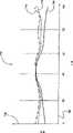
图4是绘示垫组件106的电极144的仰视图,其中该垫组件106具有叠印于其上的基材120。在操作时,基材120被置放在垫组件106的相对侧而非电极144。在一实施例中,电极144之内电极区段210A-210B个别地具有比外电极区段210C-210F更大的宽度402A-402B。内电极区段210A-210B位于垫组件106之处理区域404的下方而超过处理区域404的一半,其中该处理区域404被定义为当基材120在其径向最外边研磨位置时与基材120的外缘相切的虚线402的内部。电极区段210C-210E(其中在处理期间基材120的边缘是花最多时间于电极区段210C-210E上方)一般具有较短的宽度410C-410E,并且在一实施例中,电极区段210D具有小于邻近电极210C、210E的更短宽度。在图4所绘示的实施例中,外电极区段的至少一个被设置在界定处理区域404的线402的外面,如同图4实施例中的电极区段210F所显示。4 is a bottom
图5是为一图,其绘示出当每一电极区段210C-210F在处理期间被施加同样偏压时,对于每一电极区段210C-210F随着径向基材位置的研磨速率贡献百分比的曲线510A-510F。研磨速率贡献百分比被绘制在y轴502上,而基材上的径向位置被绘制在x轴504上。如图5所示,与外电极区段210C-210F比较时,内电极区段210A-210B对于基材120之内区域的材料移除具有更大的贡献。内电极区段210A-210B对于局部研磨速率的贡献在接近基材周围时减少了,而外电极区段210C-210E在基材周围处对于材料移除是增加了。因为最外边电极区段210F被设置在制成区域404外面,至电极区段210F的电源对于研磨速率的贡献极小。因此,由图500可显示出,研磨速率轮廓可以通过使用占大多数地设置在基材边缘内而不对基材边缘处研磨速率有大效应的电极区段而被微调。故,通过具有许多邻近于基材边缘的电极区段,且通过建构具有窄宽度之外电极区段,边缘轮廓控制可以自基材中心的轮廓控制而被退耦,以产生改善的基材处理控制与均匀性。FIG. 5 is a graph showing the grinding rate contribution for each
再者,已经发现到的是,通过将所选择的位于处理区域404外面的电极区段(例如电极区段210F)的极性逆转与/或通过施加一正偏压至固持环126,介于基材与研磨表面104之间在基材周围外面的一电压梯度可以被移动且/或维持住。控制电压梯度的位置可使得在基材周围处的研磨速率更稳定地被控制。Furthermore, it has been found that by reversing the polarity of selected electrode segments outside of the processing region 404 (eg,
图6为用以在一Ecmp制程中控制研磨轮廓的方法600的实施例的流程图。方法600开始于步骤602,其是通过在一Ecmp站100中设置一基材120于一研磨表面104上。在步骤604,电解质被提供于介于基材与位于研磨表面144下方的电极144之间以在其间建立一导电路径。如前所述,电极144可以包括一或多个独立可施加偏压的电极区段。FIG. 6 is a flowchart of an embodiment of a
在步骤606,一电性偏压被建立在基材与电极144之间。在一实施例中,电性偏压可以在电极区段之间被独立地控制,使得一局部研磨速率被建立在基材的不同部分与电极之间,藉此促进移除轮廓控制。在一Ecmp站施加偏压予一电极以促进研磨控制的范例(其是可获益自本发明)是描述于美国专利申请案号US10/244,688(公元2002年9月16日申请)、美国专利申请案号US10/456,851(公元2003年6月6日申请)、美国专利申请案号US10/949,160(公元2004年9月24日申请)、美国专利申请案号US10/940,603(公元2004年9月14日申请)中。At
电源166是适用以将电极区段210A-210F施加正与负偏压。电源166可以控制地提供介于-5至+7VDC至电极144、接触构件134与/或环126。The
在图2A绘示的操作模式的简化说明中,当施加在电极144与基材之间的偏压为约3.5VDC时,在介于基材与研磨表面之间的一包含区域250中的电解质电压大致上是维持于约-1.5VDC。由于在研磨表面104上一自由区域254(其中该自由区域254被定义在研磨头122之外)中的电解质位于约-2.5VDC的电位,一过渡梯度是存在于邻近基材边缘处,被显示为过渡梯度252。换言之,过渡区域252具有一大电压梯度,其中电解质中电压在一短时间内自-1.5VDC迅速增加至-2.5VDC。由于过渡区域252中的过渡梯度具有比包含区域250中电压高得多的电压,相较于横越在基材120中心上方的包含区域250的速率而言,在邻近过渡区域252的基材边缘的局部研磨速率具有一更快得多的移除速率。其它人相信的是,如同被通过电极与基材之间电位差所建立的电位轮廓所影响一样,此效应可以被电场线的分布与/或形状所引起。In a simplified illustration of the mode of operation depicted in FIG. 2A , when a bias voltage of about 3.5 VDC is applied between the
为了较佳控制在过渡区域252的研磨速率,过渡梯度被维持在基材120边缘之外(步骤608)。过渡梯度可以经由至少两方法来维持基材120边缘之外的过渡梯度。在一实施例中,邻近于与/或在研磨区域之外的一或多个电极区段被施加偏压以一极性,其中该极性是相反于在研磨区域内的电极区段的极性。例如,最外边电极区段210F可以被正施加偏压以小于约0VDC的一电压,并且在一实施例中被施加偏压以约0至约+5VDC,并且在又另一实施例中被施加偏压以小于约+2VDC。外电极区段210F(相对于内电极区段)的逆极性造成具有电压梯度的过渡区域252向外偏移,如图2B所示。由于较高电压是“被限制”至基材之外的一区域,设置在研磨区域下方的电极区段可更有效地控制研磨轮廓,藉此减少且/或实质上消除传统研磨例行程序中的快速边缘研磨。在一实施例中,施加至电极区段的电压是参考自基材(亦即基材提供一0VDC参考值)。To better control the grinding rate at the
在另一实施例中,步骤608可以通过施加一正偏压至固持环126的一导电部分来实施。例如,一大于0的电压(例如约1VDC)可以被施加至固持环126以将过渡区域252移动于研磨区域404之外,如图2B所示。在另一实施例中,施加至环126的电压是介于约0至约3VDC之间。在又另一实施例中,一逆极性可以被施加至外电极(相对于基材下方的电极区段)而固持环被施加正偏压。In another embodiment, step 608 may be implemented by applying a positive bias to a conductive portion of the retaining
当决定一终点时,方法600被终止于步骤610。终点可以由其它适当终点侦测技术之外的研磨时间、涡流侦测、干涉计、光学技术、电压、电荷或电流侦测而被决定。适当终点技术的范例(其可获益自本发明)是描述于先前参照的美国专利申请案US10/244,688、US10/456,851、US10/949,160与US10/940,603中。亦可以使用一选择性的过度研磨步骤612以移除残余的导电材料。The
图7-8是绘示使用方法600处理基材的一些优点。图7为一图700,其绘制出横越如前述所处理基材半径的厚度轮廓的曲线706、710、714。厚度被绘制在y轴702上,而横越基材的半径被绘制在x轴704上。曲线706描绘出逆偏压并没有被施加至外电极的一电研磨制程。如图7所示,曲线706接近外半径区域而减少的厚度显示出快速边缘研磨。相对地,曲线710与714在处理期间具有较大的厚度均匀性。曲线710代表了一基材在电化学研磨制程之后的厚度轮廓,其中在研磨区域之外的一电极被施加偏压以约-2V,而在研磨区域内的电极被施加正偏压。曲线714描绘出一研磨制程的厚度轮廓,其中在研磨区域之外的电极被施加偏压以一更大的电压(与曲线710所表示的制程比较时)。如图7所示,相较于曲线710而言,曲线714的制程具有一更慢的边缘研磨,藉此说明负偏压在边缘快速研磨上的效应。类似的结果可以通过施加一正偏压至固持环226来达到。而且,一副偏压可以被施加至外电极而施加一正偏压至固持环以进一步调整研磨制程以控制边缘快速研磨均匀性。7-8 illustrate some of the advantages of using the
边缘空白处的控制亦可以通过将外电极施加负偏压与/或将固持环126施加偏压而有利地被控制。如图8所示,一基材800典型地包括有一空白区域812,其是分开了在基材800的周围802的导电覆盖区域814。线810是描绘了在处理前导电材料覆盖区域814的程度。在处理期间,当导电材料被移除时,导电材料区域814的直径是由外直径802往后退。例如,在具有边缘快速研磨趋势的传统制程中,导电材料区域814的边缘会往后退一不乐见的自周围802距离,如线804所示。通过施加一负偏压至外电极与/或施加一正偏压至固持环126,导电材料区域814的边缘可以被维持成更靠近于其于810在预处理位置的原始位置,如线806、808所示。线806代表了使用了约2V的负偏压的导电材料覆盖区域814的边缘的位置。线808代表了使用了约4V的负偏压的导电材料覆盖区域814的边缘的位置。如图8所示,将研磨区域外的偏压逆向且/或施加一正偏压至固持环在处理期间有利地减少了于蚀刻空白处的不乐见的成长。Control of margin margins may also advantageously be controlled by negatively biasing the outer electrodes and/or biasing the retaining
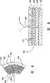
图9描绘了一研磨垫组件900的替代性实施例,其中该研磨垫组件900是可以被使用于Ecmp站100中以实施方法600。研磨垫组件900大致上包括有一导电研磨表面902、一次垫904与一电极906。次垫904与电极906是类似于前述次垫211与区段化的电极144。FIG. 9 depicts an alternative embodiment of a
耦接至一电源166的导电研磨表面902被使用以取代接触构件134以在处理期间将基材120相对于电极906施加偏压。导电研磨表面902可以由一导电材料所制成,例如先前参照的美国专利申请案的不同垫实施例中的导电材料。A conductive
在一实施例中,导电研磨表面902至少包含一聚合材料,其中该聚合材料具有设置于其内的导电材料。例如,导电研磨表面902可以具有镍、铜、金、碳与/或设置在一聚合物黏结剂中的锡粒子。研磨表面902可以包括一导电织物,例如涂覆铜的尼龙材料。导电织物可以被覆盖以一层导电聚合物,例如前述材料。In one embodiment, the conductive
导电研磨表面902可以被浮雕化或纹路化。导电研磨表面902可以包括一或多个非导电材料的岛,例如聚氨基甲酸酯细长条。导电研磨表面902亦可以包括研磨料。The conductive
导电研磨表面902包括数个通道218以允许电解质建立一导电路径于介于导电研磨表面902的上表面与电极906之间,其中该电解质位于导电研磨表面902上。电解质可以经由一通道或使用被支撑在导电研磨表面902上方的一出口而被提供穿过垫组件900,如图1所示。Conductive
因此,本发明是提供一种方法与设备,其可有利地促进轮廓控制而减少边缘快速研磨效应。再者,本发明对于基材研磨结果提供了边缘排除的更佳控制以获致更大组件产率与更大基材。Accordingly, the present invention provides a method and apparatus that advantageously facilitates contour control while reducing edge grinding effects. Furthermore, the present invention provides better control over edge exclusion for substrate grinding results resulting in greater device yields and larger substrates.
本文所描述的不同实施例的构件并非为彼此排除的,反之,该些构件可以被结合以形成本发明其它实施例。虽然前述是着重于本发明实施例,在不脱离本发明基本范围下,是可以建构出本发明的其它与进一步实施例,并且本发明的范围是由权利要求所决定。The components of the different embodiments described herein are not mutually exclusive, but rather these components may be combined to form other embodiments of the invention. While the foregoing has focused on embodiments of the invention, other and further embodiments of the invention can be constructed without departing from the basic scope of the invention, and the scope of the invention is defined by the claims.
Claims (16)
Translated fromChineseApplications Claiming Priority (2)
| Application Number | Priority Date | Filing Date | Title |
|---|---|---|---|
| US11/043,570US7655565B2 (en) | 2005-01-26 | 2005-01-26 | Electroprocessing profile control |
| US11/043,570 | 2005-01-26 |
Related Parent Applications (1)
| Application Number | Title | Priority Date | Filing Date |
|---|---|---|---|
| CNA2006800029291ADivisionCN101107090A (en) | 2005-01-26 | 2006-01-24 | Electroprocessing Contour Control |
Publications (1)
| Publication Number | Publication Date |
|---|---|
| CN101480743Atrue CN101480743A (en) | 2009-07-15 |
Family
ID=36587252
Family Applications (3)
| Application Number | Title | Priority Date | Filing Date |
|---|---|---|---|
| CNA2006800029291APendingCN101107090A (en) | 2005-01-26 | 2006-01-24 | Electroprocessing Contour Control |
| CNA2007101669018APendingCN101143433A (en) | 2005-01-26 | 2006-01-24 | Electroprocessing Contour Control |
| CNA2008101757013APendingCN101480743A (en) | 2005-01-26 | 2006-01-24 | Electroprocessing profile control |
Family Applications Before (2)
| Application Number | Title | Priority Date | Filing Date |
|---|---|---|---|
| CNA2006800029291APendingCN101107090A (en) | 2005-01-26 | 2006-01-24 | Electroprocessing Contour Control |
| CNA2007101669018APendingCN101143433A (en) | 2005-01-26 | 2006-01-24 | Electroprocessing Contour Control |
Country Status (6)
| Country | Link |
|---|---|
| US (3) | US7655565B2 (en) |
| JP (1) | JP2008528308A (en) |
| KR (1) | KR20070095396A (en) |
| CN (3) | CN101107090A (en) |
| TW (1) | TWI286960B (en) |
| WO (1) | WO2006081285A2 (en) |
Cited By (1)
| Publication number | Priority date | Publication date | Assignee | Title |
|---|---|---|---|---|
| CN105316754A (en)* | 2014-07-29 | 2016-02-10 | 盛美半导体设备(上海)有限公司 | Electrochemical machining process and device |
Families Citing this family (23)
| Publication number | Priority date | Publication date | Assignee | Title |
|---|---|---|---|---|
| US6848970B2 (en) | 2002-09-16 | 2005-02-01 | Applied Materials, Inc. | Process control in electrochemically assisted planarization |
| US20050121141A1 (en)* | 2003-11-13 | 2005-06-09 | Manens Antoine P. | Real time process control for a polishing process |
| US7422982B2 (en)* | 2006-07-07 | 2008-09-09 | Applied Materials, Inc. | Method and apparatus for electroprocessing a substrate with edge profile control |
| US9677188B2 (en) | 2009-06-17 | 2017-06-13 | Novellus Systems, Inc. | Electrofill vacuum plating cell |
| JP4680314B1 (en)* | 2010-02-04 | 2011-05-11 | 東邦エンジニアリング株式会社 | Auxiliary plate for polishing pad and method for regenerating polishing pad using the same |
| US8992757B2 (en)* | 2010-05-19 | 2015-03-31 | Novellus Systems, Inc. | Through silicon via filling using an electrolyte with a dual state inhibitor |
| WO2012033906A2 (en) | 2010-09-09 | 2012-03-15 | University Of Florida Research Foundation Inc. | Context-sensitive flow interrupter and drainage outflow optimization system |
| US8439994B2 (en) | 2010-09-30 | 2013-05-14 | Nexplanar Corporation | Method of fabricating a polishing pad with an end-point detection region for eddy current end-point detection |
| US8657653B2 (en) | 2010-09-30 | 2014-02-25 | Nexplanar Corporation | Homogeneous polishing pad for eddy current end-point detection |
| US8628384B2 (en) | 2010-09-30 | 2014-01-14 | Nexplanar Corporation | Polishing pad for eddy current end-point detection |
| ES2766834T3 (en) | 2012-05-10 | 2020-06-15 | Renishaw Plc | Manufacturing method of an item |
| IN2014DN09562A (en) | 2012-05-10 | 2015-07-17 | Renishaw Plc | |
| GB201210120D0 (en)* | 2012-05-10 | 2012-07-25 | Renishaw Plc | Laser sintered part and method of manufacture |
| JP5590477B2 (en)* | 2013-04-19 | 2014-09-17 | 株式会社ニコン | Polishing equipment |
| US9844800B2 (en)* | 2014-04-23 | 2017-12-19 | Applied Materials, Inc. | Systems, methods and apparatus for post-chemical mechanical planarization substrate cleaning |
| CN109702281B (en)* | 2019-01-31 | 2021-04-02 | 上海交通大学 | Electric arc grinding composite tool electrode |
| US11491605B2 (en)* | 2019-06-10 | 2022-11-08 | Rohm And Haas Electronic Materials Cmp Holdings, Inc. | Fluopolymer composite CMP polishing method |
| JP7654419B2 (en)* | 2020-02-19 | 2025-04-01 | 住友化学株式会社 | Polishing Pads |
| US20210323117A1 (en) | 2020-04-16 | 2021-10-21 | Applied Materials, Inc. | High throughput polishing modules and modular polishing systems |
| US11705354B2 (en) | 2020-07-10 | 2023-07-18 | Applied Materials, Inc. | Substrate handling systems |
| US12198944B2 (en) | 2020-11-11 | 2025-01-14 | Applied Materials, Inc. | Substrate handling in a modular polishing system with single substrate cleaning chambers |
| CN116079580A (en)* | 2023-02-03 | 2023-05-09 | 北京晶亦精微科技股份有限公司 | An electrochemical mechanical polishing device |
| US12224186B2 (en) | 2023-04-03 | 2025-02-11 | Applied Materials, Inc. | Apparatus and method of brush cleaning using periodic chemical treatments |
Family Cites Families (118)
| Publication number | Priority date | Publication date | Assignee | Title |
|---|---|---|---|---|
| US479389A (en)* | 1892-07-19 | Ten o nin g - iv | ||
| US3162588A (en) | 1961-04-17 | 1964-12-22 | Hammond Machinery Builders Inc | Belt type electrolytic grinding machine |
| US3448023A (en)* | 1966-01-20 | 1969-06-03 | Hammond Machinery Builders Inc | Belt type electro-chemical (or electrolytic) grinding machine |
| US3873512A (en)* | 1973-04-30 | 1975-03-25 | Martin Marietta Corp | Machining method |
| GB1539309A (en)* | 1976-12-14 | 1979-01-31 | Inoue Japax Res | Electrochemical polishing |
| US4119515A (en)* | 1977-03-28 | 1978-10-10 | National Steel Corporation | Apparatus for electroplating sheet metals |
| JPS62127492A (en) | 1985-11-26 | 1987-06-09 | Shigeo Hoshino | Electroplating method using carbon fiber |
| US4839993A (en)* | 1986-01-28 | 1989-06-20 | Fujisu Limited | Polishing machine for ferrule of optical fiber connector |
| US4793895A (en) | 1988-01-25 | 1988-12-27 | Ibm Corporation | In situ conductivity monitoring technique for chemical/mechanical planarization endpoint detection |
| JPH01193166A (en) | 1988-01-28 | 1989-08-03 | Showa Denko Kk | Pad for specularly grinding semiconductor wafer |
| US4934102A (en)* | 1988-10-04 | 1990-06-19 | International Business Machines Corporation | System for mechanical planarization |
| US4965141A (en)* | 1988-11-07 | 1990-10-23 | Nikon Corporation | Electric cell housing device for camera |
| CH678156A5 (en)* | 1989-03-20 | 1991-08-15 | Exnii Metallorezh Stankov | |
| US5136817A (en)* | 1990-02-28 | 1992-08-11 | Nihon Dempa Kogyo Co., Ltd. | Automatic lapping apparatus for piezoelectric materials |
| US5081421A (en) | 1990-05-01 | 1992-01-14 | At&T Bell Laboratories | In situ monitoring technique and apparatus for chemical/mechanical planarization endpoint detection |
| US5096550A (en) | 1990-10-15 | 1992-03-17 | The United States Of America As Represented By The United States Department Of Energy | Method and apparatus for spatially uniform electropolishing and electrolytic etching |
| US5217586A (en)* | 1992-01-09 | 1993-06-08 | International Business Machines Corporation | Electrochemical tool for uniform metal removal during electropolishing |
| US5225034A (en)* | 1992-06-04 | 1993-07-06 | Micron Technology, Inc. | Method of chemical mechanical polishing predominantly copper containing metal layers in semiconductor processing |
| MY114512A (en)* | 1992-08-19 | 2002-11-30 | Rodel Inc | Polymeric substrate with polymeric microelements |
| US5562529A (en)* | 1992-10-08 | 1996-10-08 | Fujitsu Limited | Apparatus and method for uniformly polishing a wafer |
| US6068818A (en)* | 1993-11-01 | 2000-05-30 | Nanogen, Inc. | Multicomponent devices for molecular biological analysis and diagnostics |
| US5534106A (en)* | 1994-07-26 | 1996-07-09 | Kabushiki Kaisha Toshiba | Apparatus for processing semiconductor wafers |
| US5567300A (en)* | 1994-09-02 | 1996-10-22 | Ibm Corporation | Electrochemical metal removal technique for planarization of surfaces |
| US6017265A (en)* | 1995-06-07 | 2000-01-25 | Rodel, Inc. | Methods for using polishing pads |
| US5486282A (en)* | 1994-11-30 | 1996-01-23 | Ibm Corporation | Electroetching process for seed layer removal in electrochemical fabrication of wafers |
| JP3411434B2 (en)* | 1994-12-27 | 2003-06-03 | シャープ株式会社 | Image forming device |
| US5893796A (en)* | 1995-03-28 | 1999-04-13 | Applied Materials, Inc. | Forming a transparent window in a polishing pad for a chemical mechanical polishing apparatus |
| US5674758A (en)* | 1995-06-06 | 1997-10-07 | Regents Of The University Of California | Silicon on insulator achieved using electrochemical etching |
| US6024630A (en)* | 1995-06-09 | 2000-02-15 | Applied Materials, Inc. | Fluid-pressure regulated wafer polishing head |
| US5765446A (en)* | 1995-07-11 | 1998-06-16 | Sram Corporation | Control cable preload and sealing apparatus and system |
| US5863412A (en)* | 1995-10-17 | 1999-01-26 | Canon Kabushiki Kaisha | Etching method and process for producing a semiconductor element using said etching method |
| US5738574A (en)* | 1995-10-27 | 1998-04-14 | Applied Materials, Inc. | Continuous processing system for chemical mechanical polishing |
| US5804507A (en)* | 1995-10-27 | 1998-09-08 | Applied Materials, Inc. | Radially oscillating carousel processing system for chemical mechanical polishing |
| US5575706A (en)* | 1996-01-11 | 1996-11-19 | Taiwan Semiconductor Manufacturing Company Ltd. | Chemical/mechanical planarization (CMP) apparatus and polish method |
| US5645737A (en)* | 1996-02-21 | 1997-07-08 | Micron Technology, Inc. | Wet clean for a surface having an exposed silicon/silica interface |
| US5766446A (en)* | 1996-03-05 | 1998-06-16 | Candescent Technologies Corporation | Electrochemical removal of material, particularly excess emitter material in electron-emitting device |
| US5637031A (en)* | 1996-06-07 | 1997-06-10 | Industrial Technology Research Institute | Electrochemical simulator for chemical-mechanical polishing (CMP) |
| US5871392A (en)* | 1996-06-13 | 1999-02-16 | Micron Technology, Inc. | Under-pad for chemical-mechanical planarization of semiconductor wafers |
| US6056851A (en)* | 1996-06-24 | 2000-05-02 | Taiwan Semiconductor Manufacturing Company | Slurry supply system for chemical mechanical polishing |
| US6921467B2 (en)* | 1996-07-15 | 2005-07-26 | Semitool, Inc. | Processing tools, components of processing tools, and method of making and using same for electrochemical processing of microelectronic workpieces |
| US5846882A (en) | 1996-10-03 | 1998-12-08 | Applied Materials, Inc. | Endpoint detector for a chemical mechanical polishing system |
| US6011008A (en)* | 1997-01-08 | 2000-01-04 | Yissum Research Developement Company Of The Hebrew University Of Jerusalem | Conjugates of biologically active substances |
| FR2758285B3 (en)* | 1997-01-13 | 1998-12-04 | Struers As | METHOD OF FIXING AN ABRASIVE OR POLISHING AGENT, IN THE FORM OF A SHEET, ON A MAGNETIC SUPPORT |
| US6020264A (en)* | 1997-01-31 | 2000-02-01 | International Business Machines Corporation | Method and apparatus for in-line oxide thickness determination in chemical-mechanical polishing |
| US5938801A (en)* | 1997-02-12 | 1999-08-17 | Micron Technology, Inc. | Polishing pad and a method for making a polishing pad with covalently bonded particles |
| US5807165A (en)* | 1997-03-26 | 1998-09-15 | International Business Machines Corporation | Method of electrochemical mechanical planarization |
| US5911619A (en)* | 1997-03-26 | 1999-06-15 | International Business Machines Corporation | Apparatus for electrochemical mechanical planarization |
| US5990010A (en)* | 1997-04-08 | 1999-11-23 | Lsi Logic Corporation | Pre-conditioning polishing pads for chemical-mechanical polishing |
| JPH10329007A (en)* | 1997-05-28 | 1998-12-15 | Sony Corp | Chemical machine polishing device |
| JPH1148609A (en)* | 1997-08-04 | 1999-02-23 | Fuji Xerox Co Ltd | Method and device for image recording |
| US5931719A (en)* | 1997-08-25 | 1999-08-03 | Lsi Logic Corporation | Method and apparatus for using pressure differentials through a polishing pad to improve performance in chemical mechanical polishing |
| US6103096A (en)* | 1997-11-12 | 2000-08-15 | International Business Machines Corporation | Apparatus and method for the electrochemical etching of a wafer |
| WO1999026758A1 (en)* | 1997-11-25 | 1999-06-03 | John Hopkins University | Electrochemical-control of abrasive polishing and machining rates |
| US6153043A (en)* | 1998-02-06 | 2000-11-28 | International Business Machines Corporation | Elimination of photo-induced electrochemical dissolution in chemical mechanical polishing |
| KR100474746B1 (en)* | 1998-02-12 | 2005-03-08 | 에이씨엠 리서치, 인코포레이티드 | Plating apparatus and method |
| US6004880A (en)* | 1998-02-20 | 1999-12-21 | Lsi Logic Corporation | Method of single step damascene process for deposition and global planarization |
| JP3295888B2 (en) | 1998-04-22 | 2002-06-24 | 株式会社藤森技術研究所 | Polishing dresser for polishing machine of chemical machine polisher |
| US6051500A (en) | 1998-05-19 | 2000-04-18 | Lucent Technologies Inc. | Device and method for polishing a semiconductor substrate |
| US6210257B1 (en)* | 1998-05-29 | 2001-04-03 | Micron Technology, Inc. | Web-format polishing pads and methods for manufacturing and using web-format polishing pads in mechanical and chemical-mechanical planarization of microelectronic substrates |
| US6447668B1 (en)* | 1998-07-09 | 2002-09-10 | Acm Research, Inc. | Methods and apparatus for end-point detection |
| US6395152B1 (en)* | 1998-07-09 | 2002-05-28 | Acm Research, Inc. | Methods and apparatus for electropolishing metal interconnections on semiconductor devices |
| US6248222B1 (en)* | 1998-09-08 | 2001-06-19 | Acm Research, Inc. | Methods and apparatus for holding and positioning semiconductor workpieces during electropolishing and/or electroplating of the workpieces |
| US6159079A (en) | 1998-09-08 | 2000-12-12 | Applied Materials, Inc. | Carrier head for chemical mechanical polishing a substrate |
| US6176992B1 (en)* | 1998-11-03 | 2001-01-23 | Nutool, Inc. | Method and apparatus for electro-chemical mechanical deposition |
| JP2000141215A (en)* | 1998-11-05 | 2000-05-23 | Sony Corp | Flattening grinding device and its method |
| US6541381B2 (en) | 1998-11-06 | 2003-04-01 | Beaver Creek Concepts Inc | Finishing method for semiconductor wafers using a lubricating boundary layer |
| US6726823B1 (en)* | 1998-11-28 | 2004-04-27 | Acm Research, Inc. | Methods and apparatus for holding and positioning semiconductor workpieces during electropolishing and/or electroplating of the workpieces |
| US6497800B1 (en) | 2000-03-17 | 2002-12-24 | Nutool Inc. | Device providing electrical contact to the surface of a semiconductor workpiece during metal plating |
| US6413388B1 (en)* | 2000-02-23 | 2002-07-02 | Nutool Inc. | Pad designs and structures for a versatile materials processing apparatus |
| US6251235B1 (en)* | 1999-03-30 | 2001-06-26 | Nutool, Inc. | Apparatus for forming an electrical contact with a semiconductor substrate |
| US6409904B1 (en)* | 1998-12-01 | 2002-06-25 | Nutool, Inc. | Method and apparatus for depositing and controlling the texture of a thin film |
| US6328872B1 (en)* | 1999-04-03 | 2001-12-11 | Nutool, Inc. | Method and apparatus for plating and polishing a semiconductor substrate |
| JP2000208456A (en)* | 1999-01-07 | 2000-07-28 | Fujitsu Ltd | Selective chemical mechanical polishing method |
| US6244935B1 (en) | 1999-02-04 | 2001-06-12 | Applied Materials, Inc. | Apparatus and methods for chemical mechanical polishing with an advanceable polishing sheet |
| US6066030A (en)* | 1999-03-04 | 2000-05-23 | International Business Machines Corporation | Electroetch and chemical mechanical polishing equipment |
| US6217426B1 (en)* | 1999-04-06 | 2001-04-17 | Applied Materials, Inc. | CMP polishing pad |
| US6238271B1 (en) | 1999-04-30 | 2001-05-29 | Speed Fam-Ipec Corp. | Methods and apparatus for improved polishing of workpieces |
| US20020077037A1 (en)* | 1999-05-03 | 2002-06-20 | Tietz James V. | Fixed abrasive articles |
| US6156124A (en) | 1999-06-18 | 2000-12-05 | Applied Materials, Inc. | Wafer transfer station for a chemical mechanical polisher |
| US6381169B1 (en)* | 1999-07-01 | 2002-04-30 | The Regents Of The University Of California | High density non-volatile memory device |
| US6297159B1 (en)* | 1999-07-07 | 2001-10-02 | Advanced Micro Devices, Inc. | Method and apparatus for chemical polishing using field responsive materials |
| US6234870B1 (en)* | 1999-08-24 | 2001-05-22 | International Business Machines Corporation | Serial intelligent electro-chemical-mechanical wafer processor |
| US6406363B1 (en)* | 1999-08-31 | 2002-06-18 | Lam Research Corporation | Unsupported chemical mechanical polishing belt |
| US6379223B1 (en)* | 1999-11-29 | 2002-04-30 | Applied Materials, Inc. | Method and apparatus for electrochemical-mechanical planarization |
| US6368184B1 (en)* | 2000-01-06 | 2002-04-09 | Advanced Micro Devices, Inc. | Apparatus for determining metal CMP endpoint using integrated polishing pad electrodes |
| US6630059B1 (en)* | 2000-01-14 | 2003-10-07 | Nutool, Inc. | Workpeice proximity plating apparatus |
| US6368190B1 (en)* | 2000-01-26 | 2002-04-09 | Agere Systems Guardian Corp. | Electrochemical mechanical planarization apparatus and method |
| US7077721B2 (en)* | 2000-02-17 | 2006-07-18 | Applied Materials, Inc. | Pad assembly for electrochemical mechanical processing |
| US20030213703A1 (en)* | 2002-05-16 | 2003-11-20 | Applied Materials, Inc. | Method and apparatus for substrate polishing |
| US6991528B2 (en) | 2000-02-17 | 2006-01-31 | Applied Materials, Inc. | Conductive polishing article for electrochemical mechanical polishing |
| US7125477B2 (en)* | 2000-02-17 | 2006-10-24 | Applied Materials, Inc. | Contacts for electrochemical processing |
| US7066800B2 (en)* | 2000-02-17 | 2006-06-27 | Applied Materials Inc. | Conductive polishing article for electrochemical mechanical polishing |
| US6797623B2 (en)* | 2000-03-09 | 2004-09-28 | Sony Corporation | Methods of producing and polishing semiconductor device and polishing apparatus |
| US6482307B2 (en)* | 2000-05-12 | 2002-11-19 | Nutool, Inc. | Method of and apparatus for making electrical contact to wafer surface for full-face electroplating or electropolishing |
| US6582281B2 (en)* | 2000-03-23 | 2003-06-24 | Micron Technology, Inc. | Semiconductor processing methods of removing conductive material |
| JP2001269862A (en)* | 2000-03-27 | 2001-10-02 | Toshiba Corp | Polishing pad, polishing apparatus and polishing method |
| US6402591B1 (en)* | 2000-03-31 | 2002-06-11 | Lam Research Corporation | Planarization system for chemical-mechanical polishing |
| US6689257B2 (en)* | 2000-05-26 | 2004-02-10 | Ebara Corporation | Substrate processing apparatus and substrate plating apparatus |
| US6358118B1 (en)* | 2000-06-30 | 2002-03-19 | Lam Research Corporation | Field controlled polishing apparatus and method |
| US7112121B2 (en)* | 2000-08-30 | 2006-09-26 | Micron Technology, Inc. | Methods and apparatus for electrical, mechanical and/or chemical removal of conductive material from a microelectronic substrate |
| US7160176B2 (en)* | 2000-08-30 | 2007-01-09 | Micron Technology, Inc. | Methods and apparatus for electrically and/or chemically-mechanically removing conductive material from a microelectronic substrate |
| JP2002093761A (en)* | 2000-09-19 | 2002-03-29 | Sony Corp | Polishing method, polishing system, plating method and plating system |
| US6736952B2 (en) | 2001-02-12 | 2004-05-18 | Speedfam-Ipec Corporation | Method and apparatus for electrochemical planarization of a workpiece |
| US6811680B2 (en)* | 2001-03-14 | 2004-11-02 | Applied Materials Inc. | Planarization of substrates using electrochemical mechanical polishing |
| US6899804B2 (en)* | 2001-04-10 | 2005-05-31 | Applied Materials, Inc. | Electrolyte composition and treatment for electrolytic chemical mechanical polishing |
| US7232514B2 (en)* | 2001-03-14 | 2007-06-19 | Applied Materials, Inc. | Method and composition for polishing a substrate |
| US6638863B2 (en)* | 2001-04-24 | 2003-10-28 | Acm Research, Inc. | Electropolishing metal layers on wafers having trenches or vias with dummy structures |
| CN100398261C (en) | 2001-04-24 | 2008-07-02 | 应用材料有限公司 | Conductive Polishing Parts for Electrochemical Mechanical Polishing |
| JP3807295B2 (en)* | 2001-11-30 | 2006-08-09 | ソニー株式会社 | Polishing method |
| US6776693B2 (en)* | 2001-12-19 | 2004-08-17 | Applied Materials Inc. | Method and apparatus for face-up substrate polishing |
| US6837983B2 (en) | 2002-01-22 | 2005-01-04 | Applied Materials, Inc. | Endpoint detection for electro chemical mechanical polishing and electropolishing processes |
| JP4076430B2 (en)* | 2002-01-31 | 2008-04-16 | 株式会社荏原製作所 | Substrate processing equipment |
| WO2003090962A1 (en)* | 2002-04-23 | 2003-11-06 | Koninklijke Philips Electronics N.V. | A method, an apparatus,a control system and a computer program to perform an automatic removal of cathode depositions during a bi polar electrochemical machining |
| US6689258B1 (en)* | 2002-04-30 | 2004-02-10 | Advanced Micro Devices, Inc. | Electrochemically generated reactants for chemical mechanical planarization |
| JP2003347243A (en)* | 2002-05-27 | 2003-12-05 | Sony Corp | Polishing method, polishing device, and method of manufacturing semiconductor device |
| WO2004072332A1 (en)* | 2003-02-12 | 2004-08-26 | Ebara Corporation | Polishing fluid, method of polishing, and polishing apparatus |
| US7090576B2 (en)* | 2003-06-30 | 2006-08-15 | Microsoft Corporation | Personalized behavior of computer controlled avatars in a virtual reality environment |
| US7084064B2 (en)* | 2004-09-14 | 2006-08-01 | Applied Materials, Inc. | Full sequence metal and barrier layer electrochemical mechanical processing |
- 2005
- 2005-01-26USUS11/043,570patent/US7655565B2/ennot_activeExpired - Fee Related
- 2006
- 2006-01-24CNCNA2006800029291Apatent/CN101107090A/enactivePending
- 2006-01-24JPJP2007553195Apatent/JP2008528308A/enactivePending
- 2006-01-24WOPCT/US2006/002595patent/WO2006081285A2/enactiveApplication Filing
- 2006-01-24CNCNA2007101669018Apatent/CN101143433A/enactivePending
- 2006-01-24TWTW095102669Apatent/TWI286960B/ennot_activeIP Right Cessation
- 2006-01-24KRKR1020077018157Apatent/KR20070095396A/ennot_activeCeased
- 2006-01-24CNCNA2008101757013Apatent/CN101480743A/enactivePending
- 2007
- 2007-10-23USUS11/877,233patent/US7709382B2/ennot_activeExpired - Fee Related
- 2007-10-23USUS11/877,223patent/US20080047841A1/ennot_activeAbandoned
Cited By (2)
| Publication number | Priority date | Publication date | Assignee | Title |
|---|---|---|---|---|
| CN105316754A (en)* | 2014-07-29 | 2016-02-10 | 盛美半导体设备(上海)有限公司 | Electrochemical machining process and device |
| CN105316754B (en)* | 2014-07-29 | 2019-08-16 | 盛美半导体设备(上海)有限公司 | Electrochemical machining process and electrochemical machining apparatus |
Also Published As
| Publication number | Publication date |
|---|---|
| US20060166500A1 (en) | 2006-07-27 |
| US7709382B2 (en) | 2010-05-04 |
| WO2006081285A3 (en) | 2006-09-14 |
| TWI286960B (en) | 2007-09-21 |
| CN101143433A (en) | 2008-03-19 |
| JP2008528308A (en) | 2008-07-31 |
| TW200626295A (en) | 2006-08-01 |
| WO2006081285A2 (en) | 2006-08-03 |
| US20080045012A1 (en) | 2008-02-21 |
| US20080047841A1 (en) | 2008-02-28 |
| KR20070095396A (en) | 2007-09-28 |
| CN101107090A (en) | 2008-01-16 |
| US7655565B2 (en) | 2010-02-02 |
Similar Documents
| Publication | Publication Date | Title |
|---|---|---|
| CN101480743A (en) | Electroprocessing profile control | |
| US6848970B2 (en) | Process control in electrochemically assisted planarization | |
| US6776693B2 (en) | Method and apparatus for face-up substrate polishing | |
| CN100425404C (en) | Electrochemical mechanical polishing system and method for detecting polishing endpoint | |
| US7229535B2 (en) | Hydrogen bubble reduction on the cathode using double-cell designs | |
| US6991526B2 (en) | Control of removal profile in electrochemically assisted CMP | |
| US20030213703A1 (en) | Method and apparatus for substrate polishing | |
| US7186164B2 (en) | Processing pad assembly with zone control | |
| US7842169B2 (en) | Method and apparatus for local polishing control | |
| KR20030082566A (en) | Planarization of substrates using electrochemical mechanical polishing | |
| WO2004111146A1 (en) | Polishing composition and method for polishing a conductive material | |
| WO2007019279A2 (en) | Method and composition for polishing a substrate | |
| CN1531473A (en) | Conductive Polishing Parts for Electrochemical Mechanical Polishing | |
| US20100059390A1 (en) | METHOD AND APARATUS FOR ELECTROCHEMICAL MECHANICAL POLISHING NiP SUBSTRATES | |
| US20040072445A1 (en) | Effective method to improve surface finish in electrochemically assisted CMP | |
| WO2004024394A1 (en) | Control of removal profile in electrochemically assisted cmp | |
| US20080277787A1 (en) | Method and pad design for the removal of barrier material by electrochemical mechanical processing | |
| US12090600B2 (en) | Face-up wafer electrochemical planarization apparatus |
Legal Events
| Date | Code | Title | Description |
|---|---|---|---|
| C06 | Publication | ||
| PB01 | Publication | ||
| C10 | Entry into substantive examination | ||
| SE01 | Entry into force of request for substantive examination | ||
| C02 | Deemed withdrawal of patent application after publication (patent law 2001) | ||
| WD01 | Invention patent application deemed withdrawn after publication | Open date:20090715 |