CN101473064B - Silicon thin-film and method of forming silicon thin-film - Google Patents
Silicon thin-film and method of forming silicon thin-filmDownload PDFInfo
- Publication number
- CN101473064B CN101473064BCN2007800224621ACN200780022462ACN101473064BCN 101473064 BCN101473064 BCN 101473064BCN 2007800224621 ACN2007800224621 ACN 2007800224621ACN 200780022462 ACN200780022462 ACN 200780022462ACN 101473064 BCN101473064 BCN 101473064B
- Authority
- CN
- China
- Prior art keywords
- film
- thin film
- gas
- silicon
- substrate
- Prior art date
- Legal status (The legal status is an assumption and is not a legal conclusion. Google has not performed a legal analysis and makes no representation as to the accuracy of the status listed.)
- Expired - Fee Related
Links
- 239000010409thin filmSubstances0.000titleclaimsabstractdescription103
- 229910052710siliconInorganic materials0.000titleclaimsabstractdescription56
- XUIMIQQOPSSXEZ-UHFFFAOYSA-NSiliconChemical compound[Si]XUIMIQQOPSSXEZ-UHFFFAOYSA-N0.000titleclaimsabstractdescription45
- 239000010703siliconSubstances0.000titleclaimsabstractdescription44
- 238000000034methodMethods0.000titleclaimsabstractdescription43
- 239000010408filmSubstances0.000claimsabstractdescription137
- 239000007789gasSubstances0.000claimsabstractdescription73
- 239000000758substrateSubstances0.000claimsabstractdescription61
- 229910052760oxygenInorganic materials0.000claimsabstractdescription21
- QVGXLLKOCUKJST-UHFFFAOYSA-Natomic oxygenChemical compound[O]QVGXLLKOCUKJST-UHFFFAOYSA-N0.000claimsabstractdescription16
- 239000001301oxygenSubstances0.000claimsabstractdescription16
- 230000004888barrier functionEffects0.000claimsabstractdescription10
- 238000005229chemical vapour depositionMethods0.000claimsabstractdescription9
- 229910052739hydrogenInorganic materials0.000claimsabstractdescription9
- 229910052757nitrogenInorganic materials0.000claimsabstractdescription8
- IJGRMHOSHXDMSA-UHFFFAOYSA-NAtomic nitrogenChemical compoundN#NIJGRMHOSHXDMSA-UHFFFAOYSA-N0.000claimsabstractdescription6
- FFUAGWLWBBFQJT-UHFFFAOYSA-NhexamethyldisilazaneChemical compoundC[Si](C)(C)N[Si](C)(C)CFFUAGWLWBBFQJT-UHFFFAOYSA-N0.000claimsdescription23
- 230000015572biosynthetic processEffects0.000claimsdescription22
- 229910052799carbonInorganic materials0.000claimsdescription5
- 238000009413insulationMethods0.000claims2
- 150000003376siliconChemical class0.000claims2
- YZCKVEUIGOORGS-IGMARMGPSA-NProtiumChemical compound[1H]YZCKVEUIGOORGS-IGMARMGPSA-N0.000claims1
- 241000720974ProtiumSpecies0.000claims1
- 238000003475laminationMethods0.000claims1
- 238000005268plasma chemical vapour depositionMethods0.000abstractdescription9
- UFHFLCQGNIYNRP-UHFFFAOYSA-NHydrogenChemical compound[H][H]UFHFLCQGNIYNRP-UHFFFAOYSA-N0.000abstractdescription2
- 239000001257hydrogenSubstances0.000abstractdescription2
- 238000007789sealingMethods0.000description20
- 229910052581Si3N4Inorganic materials0.000description17
- HQVNEWCFYHHQES-UHFFFAOYSA-Nsilicon nitrideChemical compoundN12[Si]34N5[Si]62N3[Si]51N64HQVNEWCFYHHQES-UHFFFAOYSA-N0.000description17
- VYPSYNLAJGMNEJ-UHFFFAOYSA-NSilicium dioxideChemical compoundO=[Si]=OVYPSYNLAJGMNEJ-UHFFFAOYSA-N0.000description11
- 229910052814silicon oxideInorganic materials0.000description11
- 239000000203mixtureSubstances0.000description6
- 238000003860storageMethods0.000description6
- 238000012546transferMethods0.000description6
- 238000005336crackingMethods0.000description5
- QGZKDVFQNNGYKY-UHFFFAOYSA-NAmmoniaChemical compoundNQGZKDVFQNNGYKY-UHFFFAOYSA-N0.000description4
- 238000010586diagramMethods0.000description4
- 230000000694effectsEffects0.000description4
- 238000005530etchingMethods0.000description4
- 229920002799BoPETPolymers0.000description3
- 230000005540biological transmissionEffects0.000description3
- 238000005259measurementMethods0.000description3
- 238000005001rutherford backscattering spectroscopyMethods0.000description3
- 238000004544sputter depositionMethods0.000description3
- 238000006557surface reactionMethods0.000description3
- XLYOFNOQVPJJNP-UHFFFAOYSA-NwaterChemical compoundOXLYOFNOQVPJJNP-UHFFFAOYSA-N0.000description3
- QVQLCTNNEUAWMS-UHFFFAOYSA-Nbarium oxideChemical compound[Ba]=OQVQLCTNNEUAWMS-UHFFFAOYSA-N0.000description2
- 238000005401electroluminescenceMethods0.000description2
- 239000012535impuritySubstances0.000description2
- 238000009616inductively coupled plasmaMethods0.000description2
- 238000004519manufacturing processMethods0.000description2
- 239000012528membraneSubstances0.000description2
- 229920000139polyethylene terephthalatePolymers0.000description2
- 239000005020polyethylene terephthalateSubstances0.000description2
- 230000001681protective effectEffects0.000description2
- 239000002994raw materialSubstances0.000description2
- 239000011347resinSubstances0.000description2
- 229920005989resinPolymers0.000description2
- 239000004065semiconductorSubstances0.000description2
- 238000002230thermal chemical vapour depositionMethods0.000description2
- 241000907788Cordia gerascanthusSpecies0.000description1
- BLRPTPMANUNPDV-UHFFFAOYSA-NSilaneChemical compound[SiH4]BLRPTPMANUNPDV-UHFFFAOYSA-N0.000description1
- 239000006096absorbing agentSubstances0.000description1
- 229910021529ammoniaInorganic materials0.000description1
- 238000004458analytical methodMethods0.000description1
- 238000006243chemical reactionMethods0.000description1
- 230000000052comparative effectEffects0.000description1
- 239000000470constituentSubstances0.000description1
- 238000007796conventional methodMethods0.000description1
- 230000018044dehydrationEffects0.000description1
- 238000006297dehydration reactionMethods0.000description1
- 238000010494dissociation reactionMethods0.000description1
- 208000018459dissociative diseaseDiseases0.000description1
- 230000005684electric fieldEffects0.000description1
- 238000002474experimental methodMethods0.000description1
- 238000004880explosionMethods0.000description1
- 239000011521glassSubstances0.000description1
- 229910052736halogenInorganic materials0.000description1
- 150000002367halogensChemical class0.000description1
- 230000001939inductive effectEffects0.000description1
- 238000010030laminatingMethods0.000description1
- 238000000691measurement methodMethods0.000description1
- 238000012986modificationMethods0.000description1
- 230000004048modificationEffects0.000description1
- 229910000069nitrogen hydrideInorganic materials0.000description1
- 230000002093peripheral effectEffects0.000description1
- 239000012466permeateSubstances0.000description1
- -1polyethylene terephthalatePolymers0.000description1
- 238000012545processingMethods0.000description1
- 239000012495reaction gasSubstances0.000description1
- 229910000077silaneInorganic materials0.000description1
- 239000007787solidSubstances0.000description1
- 239000000126substanceSubstances0.000description1
- 238000012360testing methodMethods0.000description1
- 238000005979thermal decomposition reactionMethods0.000description1
- 238000007740vapor depositionMethods0.000description1
Images


Classifications
- H—ELECTRICITY
- H01—ELECTRIC ELEMENTS
- H01L—SEMICONDUCTOR DEVICES NOT COVERED BY CLASS H10
- H01L21/00—Processes or apparatus adapted for the manufacture or treatment of semiconductor or solid state devices or of parts thereof
- H01L21/02—Manufacture or treatment of semiconductor devices or of parts thereof
- H01L21/02104—Forming layers
- H01L21/02365—Forming inorganic semiconducting materials on a substrate
- H01L21/02612—Formation types
- H01L21/02617—Deposition types
- H01L21/0262—Reduction or decomposition of gaseous compounds, e.g. CVD
- C—CHEMISTRY; METALLURGY
- C23—COATING METALLIC MATERIAL; COATING MATERIAL WITH METALLIC MATERIAL; CHEMICAL SURFACE TREATMENT; DIFFUSION TREATMENT OF METALLIC MATERIAL; COATING BY VACUUM EVAPORATION, BY SPUTTERING, BY ION IMPLANTATION OR BY CHEMICAL VAPOUR DEPOSITION, IN GENERAL; INHIBITING CORROSION OF METALLIC MATERIAL OR INCRUSTATION IN GENERAL
- C23C—COATING METALLIC MATERIAL; COATING MATERIAL WITH METALLIC MATERIAL; SURFACE TREATMENT OF METALLIC MATERIAL BY DIFFUSION INTO THE SURFACE, BY CHEMICAL CONVERSION OR SUBSTITUTION; COATING BY VACUUM EVAPORATION, BY SPUTTERING, BY ION IMPLANTATION OR BY CHEMICAL VAPOUR DEPOSITION, IN GENERAL
- C23C16/00—Chemical coating by decomposition of gaseous compounds, without leaving reaction products of surface material in the coating, i.e. chemical vapour deposition [CVD] processes
- C23C16/22—Chemical coating by decomposition of gaseous compounds, without leaving reaction products of surface material in the coating, i.e. chemical vapour deposition [CVD] processes characterised by the deposition of inorganic material, other than metallic material
- C23C16/30—Deposition of compounds, mixtures or solid solutions, e.g. borides, carbides, nitrides
- C23C16/40—Oxides
- C23C16/401—Oxides containing silicon
- C—CHEMISTRY; METALLURGY
- C23—COATING METALLIC MATERIAL; COATING MATERIAL WITH METALLIC MATERIAL; CHEMICAL SURFACE TREATMENT; DIFFUSION TREATMENT OF METALLIC MATERIAL; COATING BY VACUUM EVAPORATION, BY SPUTTERING, BY ION IMPLANTATION OR BY CHEMICAL VAPOUR DEPOSITION, IN GENERAL; INHIBITING CORROSION OF METALLIC MATERIAL OR INCRUSTATION IN GENERAL
- C23C—COATING METALLIC MATERIAL; COATING MATERIAL WITH METALLIC MATERIAL; SURFACE TREATMENT OF METALLIC MATERIAL BY DIFFUSION INTO THE SURFACE, BY CHEMICAL CONVERSION OR SUBSTITUTION; COATING BY VACUUM EVAPORATION, BY SPUTTERING, BY ION IMPLANTATION OR BY CHEMICAL VAPOUR DEPOSITION, IN GENERAL
- C23C16/00—Chemical coating by decomposition of gaseous compounds, without leaving reaction products of surface material in the coating, i.e. chemical vapour deposition [CVD] processes
- C23C16/22—Chemical coating by decomposition of gaseous compounds, without leaving reaction products of surface material in the coating, i.e. chemical vapour deposition [CVD] processes characterised by the deposition of inorganic material, other than metallic material
- C23C16/30—Deposition of compounds, mixtures or solid solutions, e.g. borides, carbides, nitrides
- C23C16/42—Silicides
- H—ELECTRICITY
- H10—SEMICONDUCTOR DEVICES; ELECTRIC SOLID-STATE DEVICES NOT OTHERWISE PROVIDED FOR
- H10K—ORGANIC ELECTRIC SOLID-STATE DEVICES
- H10K59/00—Integrated devices, or assemblies of multiple devices, comprising at least one organic light-emitting element covered by group H10K50/00
- H10K59/80—Constructional details
- H10K59/87—Passivation; Containers; Encapsulations
- H10K59/873—Encapsulations
- H10K59/8731—Encapsulations multilayered coatings having a repetitive structure, e.g. having multiple organic-inorganic bilayers
- H—ELECTRICITY
- H10—SEMICONDUCTOR DEVICES; ELECTRIC SOLID-STATE DEVICES NOT OTHERWISE PROVIDED FOR
- H10K—ORGANIC ELECTRIC SOLID-STATE DEVICES
- H10K50/00—Organic light-emitting devices
- H10K50/80—Constructional details
- H10K50/84—Passivation; Containers; Encapsulations
- H10K50/844—Encapsulations
- H10K50/8445—Encapsulations multilayered coatings having a repetitive structure, e.g. having multiple organic-inorganic bilayers
Landscapes
- Chemical & Material Sciences (AREA)
- Inorganic Chemistry (AREA)
- Engineering & Computer Science (AREA)
- Organic Chemistry (AREA)
- Chemical Kinetics & Catalysis (AREA)
- Materials Engineering (AREA)
- Mechanical Engineering (AREA)
- Metallurgy (AREA)
- General Chemical & Material Sciences (AREA)
- Condensed Matter Physics & Semiconductors (AREA)
- Physics & Mathematics (AREA)
- General Physics & Mathematics (AREA)
- Manufacturing & Machinery (AREA)
- Computer Hardware Design (AREA)
- Microelectronics & Electronic Packaging (AREA)
- Power Engineering (AREA)
- Chemical Vapour Deposition (AREA)
- Electroluminescent Light Sources (AREA)
Abstract
Translated fromChinese
Description
Translated fromChinese技术领域technical field
本发明涉及硅系薄膜和硅系薄膜的形成方法。更详细地说,本发明涉及具有绝缘功能或阻隔功能的硅系薄膜以及在基板上通过CVD(化学气相沉积)法形成该硅系薄膜的方法。The present invention relates to a silicon-based thin film and a method for forming the silicon-based thin film. More specifically, the present invention relates to a silicon-based thin film having an insulating function or a barrier function and a method of forming the silicon-based thin film on a substrate by CVD (Chemical Vapor Deposition).
背景技术Background technique
氮化硅膜作为半导体器件的保护膜或绝缘膜是重要的,其形成中使用热CVD法或等离子体CVD法。热CVD法中,例如使用硅烷(SiH4)气体和氨(NH3)气体,利用750~800℃的温度下的热分解反应使氮化硅膜化学气相沉积在基板表面上。等离子体CVD法中,仍使用SiH4气体和NH3气体,对该反应气体施加高频电场,利用其电能量使气体活性化,通过等离子体反应于300℃左右的低温使氮化硅膜化学气相沉积在基板表面上。以往,如此形成的氮化硅膜存在由于水分和杂质的侵入等而易于产生裂纹、剥离的问题。A silicon nitride film is important as a protective film or an insulating film of a semiconductor device, and is formed using a thermal CVD method or a plasma CVD method. In the thermal CVD method, for example, a silicon nitride film is chemically vapor-deposited on a substrate surface by using silane (SiH4 ) gas and ammonia (NH3 ) gas by thermal decomposition reaction at a temperature of 750 to 800°C. In the plasma CVD method, SiH4 gas and NH3 gas are still used, a high-frequency electric field is applied to the reaction gas, and the gas is activated by using its electric energy, and the silicon nitride film is chemically formed by plasma reaction at a low temperature of about 300°C. Vapor deposition on the substrate surface. Conventionally, the silicon nitride film formed in this way has the problem that cracks and peeling are likely to occur due to intrusion of moisture and impurities.
作为能够不易生成裂纹、剥离的氮化硅膜的形成方法,例如专利文献1中公开了如下技术:通过使用被等离子体激发的卤素系气体,在真空条件下对基板表面进行蚀刻处理,从而完全去除残留在基板上的杂质,并且在表面上形成均匀且微细的凹凸,以试图改善氮化硅膜与基板的密合性和膜质。并且,专利文献2中公开了如下技术:在制膜室的前段设置前处理室,在该前处理室中,对基板的表面照射ECR(Electron CyclotronResonance:电子回旋共振)等离子体,使吸附于基板表面的水分和在基板上制膜而成的薄膜中所含有的水分进行脱离。As a method of forming a silicon nitride film that is less prone to cracking and peeling, for example,
专利文献1:日本特开平5-315251号公报Patent Document 1: Japanese Patent Application Laid-Open No. 5-315251
专利文献2:日本特开平5-331618号公报Patent Document 2: Japanese Patent Application Laid-Open No. 5-331618
发明内容Contents of the invention
但是,当将上述专利文献1的方法应用于形成有有机EL(ElectroLuminescence:电致发光)等电子器件的基板时,担心电子器件本身会被蚀刻掉。并且,当将上述专利文献2的方法应用于上述基板时,在进行水分的脱离时电子器件会持续暴露于ECR等离子体中,容易受到等离子体损伤。并且,由于在制膜室的前段设置前处理室而导致装置构成庞大。However, when the method of the above-mentioned
鉴于上述情况,本发明的目的在于提供一种硅系薄膜和该硅系薄膜的形成方法,该硅系薄膜和该硅系薄膜的形成方法不会对形成于基板上的电子器件造成损害且装置构成不会变得庞大,并且能够改善硅系薄膜在基板上的密合性,能够形成不易生成裂纹和剥离的硅系薄膜。In view of the foregoing, it is an object of the present invention to provide a silicon-based thin film and a method for forming the silicon-based thin film, which do not cause damage to electronic devices formed on a substrate and are capable of The structure does not become bulky, the adhesion of the silicon-based thin film to the substrate can be improved, and a silicon-based thin film that is less prone to cracking and peeling can be formed.
为了实现上述目的,本发明的硅系薄膜的形成方法是通过CVD法在基板K上形成具有绝缘功能或阻隔功能的硅系薄膜的硅系薄膜形成方法,该方法的特征在于包括如下步骤:使用含有氢元素的气体和含有硅元素的气体在所述基板K上通过等离子体CVD法形成第1薄膜11的步骤;使用含有氮元素的气体和含有硅元素的气体通过等离子体CVD法形成第2薄膜12的步骤;和使用含有氧元素的气体和含有硅元素的气体通过等离子体CVD法形成第3薄膜13的步骤。In order to achieve the above object, the method for forming a silicon-based thin film of the present invention is a method for forming a silicon-based thin film having an insulating function or a barrier function on a substrate K by a CVD method, and the method is characterized in that it includes the following steps: using A step of forming a first
优选的是,在最下层形成第1薄膜11,在第1薄膜11上交替地层积两层以上的第2薄膜12和第3薄膜13。Preferably, the first
更优选的是,按照第2薄膜以Si:H:C:N:O=1:3~4:1.5~2.5:0.3~1.5:0.5以下的组成比含有Si、H、C、N和O且第3薄膜13以Si:O=1:1.9~2.1的组成比含有Si和O的方式形成第2薄膜12和第3薄膜13。More preferably, the second thin film contains Si, H, C, N, and O at a composition ratio of Si:H:C:N:O=1:3 to 4:1.5 to 2.5:0.3 to 1.5:0.5 or less and The third
进一步优选的是,作为形成第1薄膜11、第2薄膜12和第3薄膜13时所用的含有硅元素的气体,使用HMDS(Hexa Methyl DiSilazane:六甲基二硅氮烷)气体。More preferably, HMDS (Hexa Methyl DiSilazane: hexamethyldisilazane) gas is used as the silicon element-containing gas used for forming the first
此外,本发明的硅系薄膜是具有绝缘功能或阻隔功能的硅系薄膜,该硅系薄膜的特征在于,该硅系薄膜在基板K上依次层积第1薄膜11、第2薄膜12和第3薄膜13而成,第1薄膜11含有H和Si作为构成元素,第2薄膜12以Si:H:C:N:O=1:3~4:1.5~2.5:0.3~1.5:0.5以下的组成比含有Si、H、C、N和O,第3薄膜13以Si:O=1:1.9~2.1的组成比含有Si和O。In addition, the silicon-based thin film of the present invention is a silicon-based thin film having an insulating function or a barrier function. The silicon-based thin film is characterized in that the first
优选的是,第1薄膜11形成在最下层,在第1薄膜11上交替地层积两层以上的第2薄膜12和第3薄膜13。Preferably, the first
本发明中,基板是指被赋予绝缘功能、阻隔功能的对象,并且是PET(聚对苯二甲酸乙二醇酯)膜等树脂膜本身或是在该树脂膜上形成有有机EL等电子器件的物体。In the present invention, a substrate refers to an object provided with an insulating function and a barrier function, and is a resin film such as a PET (polyethylene terephthalate) film itself or an electronic device such as an organic EL formed on the resin film. objects.
本发明能够提供一种硅系薄膜和该硅系薄膜的形成方法,该硅系薄膜和该硅系薄膜的形成方法不会对形成于基板上的电子器件造成损害且装置构成不会变得庞大,能够改善硅系薄膜在基板上的密合性,不易生成裂纹和剥离。The present invention can provide a silicon-based thin film and a method for forming the silicon-based thin film that do not damage electronic devices formed on a substrate and that do not cause bulky device configurations. , can improve the adhesion of the silicon-based thin film on the substrate, and it is not easy to generate cracks and peeling off.
附图说明Description of drawings
图1是实施本发明时使用的密封膜形成装置的正面示意图。Fig. 1 is a schematic front view of a sealing film forming apparatus used in the practice of the present invention.
图2是图1的密封膜形成装置的平面示意图。FIG. 2 is a schematic plan view of the sealing film forming device of FIG. 1 .
图3是用于说明本发明的密封膜的形成阶段的图。Fig. 3 is a diagram for explaining the formation stages of the sealing film of the present invention.
图4是用于说明本发明的密封膜的形成阶段的图。Fig. 4 is a diagram for explaining the formation stages of the sealing film of the present invention.
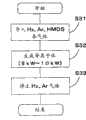
图5是显示形成本发明的密封膜的程序的流程图。Fig. 5 is a flow chart showing the procedure for forming the sealing film of the present invention.
图6是显示形成第1薄膜的程序的流程图。Fig. 6 is a flowchart showing a procedure for forming a first thin film.
图7是显示形成第2薄膜的程序的流程图。Fig. 7 is a flowchart showing a procedure for forming a second thin film.
图8是显示形成第3薄膜的程序的流程图。Fig. 8 is a flowchart showing a procedure for forming a third thin film.
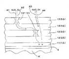
图9是用于说明本发明的密封膜捕获水分和氧的效果的图。Fig. 9 is a diagram for explaining the effect of the sealing film of the present invention in trapping moisture and oxygen.
符号说明Symbol Description
9 有机EL元件(电子器件)9 Organic EL elements (electronic devices)
11 第1薄膜11 1st film
12 第2薄膜12 Second film
13 第3薄膜13 3rd film
K 基板K Substrate
具体实施方式Detailed ways
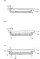
下面使用附图对本具体实施方式进行说明。图1是实施本发明时使用的密封膜形成装置的正面示意图,图2是图1的密封膜形成装置的平面示意图。需要说明的是,该密封膜形成装置是为了膜形成的实验而制作的,其与在制造有机EL基板等半导体装置的车间里的生产线上使用的装置不同。Hereinafter, this specific embodiment will be described using the drawings. FIG. 1 is a schematic front view of a sealing film forming apparatus used in carrying out the present invention, and FIG. 2 is a schematic plan view of the sealing film forming apparatus of FIG. 1 . In addition, this sealing film formation apparatus was produced for the experiment of film formation, and it is different from the apparatus used on the production line in the workshop which manufactures semiconductor devices, such as an organic EL board|substrate.
如图1所示,密封膜形成装置1具有加载互锁真空室(ロ—ドロツク室)2、与加载互锁真空室2连接设置的机器人(robot)室3以及与机器人室3连接设置的制膜室4。该密封膜形成装置1所要形成的密封膜是氮化硅系膜和氧化硅膜的层积膜。As shown in FIG. 1 , a sealing
加载互锁真空室2被制成能够通过闸阀21与机器人室3隔绝。并且,加载互锁真空室2与真空泵22连接,同时在加载互锁真空室2内部具有基板储放架(基板ストツカ—)23。基板储放架23具有用于支撑基板K的周边部的支承销(支持ピン)24。此处,基板K的尺寸为370mm×470mm,表面形成有有机EL元件9。The load
机器人室3在内部具有基板传送机器人31。基板传送机器人31具有马达32、机器手臂33和可动支持台34。可动支持台34的构成如下:通过马达32的驱动,利用机器手臂33向X、Y、Z各方向自由移动。可动支持台34具有与上述基板储放架23的支承销24相同的支承销35。The
制膜室4与机器人室3连通,并且与真空泵42、HMDS供给罐44、NH3供给罐46、H2供给罐52、Ar供给罐53、O2供给罐55连接。制膜室4通过流量控制阀41与真空泵42连接,通过流量控制阀43与HMDS供给罐44连接,通过流量控制阀45与NH3供给罐46连接,通过流量控制阀51与H2供给罐52和Ar供给罐53连接,通过流量控制阀54与O2供给罐55连接。制膜室4的内部具有环形天线(ル—プアンテナ)47。The
环形天线47是生成等离子体的单元,由绝缘管48和导电性电极49构成。2根绝缘管48在制膜室4内相互对置并平行设置。导电性电极49插入2根绝缘管48而设置,导电性电极49贯通制膜室4的相互对置的侧壁,以使导电性电极49如图2所示俯视大致呈U字形,并且导电性电极49与供给高频电流的电源50连接。高频电流50的频率优选为13.56MHz。需要说明的是,所使用的等离子体也可以是CCP(CapacitiveCoupled Plasma:电容耦合等离子体)、ICP(Inductive Coupled Plasma:电感耦合等离子体)、介质阻挡放电(バリア放電)、空心阴极放电(ホロ—放電)等。The
下面,还参照图3至图8,对本发明的密封膜的形成方法进行说明。图3、图4是用于说明本发明的密封膜的形成阶段的图,图5是显示形成本发明的密封膜的程序的流程图,图6是显示形成第1薄膜的程序的流程图,图7是显示形成第2薄膜的程序的流程图,图8是显示形成第3薄膜的程序的流程图。Next, the method for forming the sealing film of the present invention will be described with reference to FIGS. 3 to 8 . Fig. 3, Fig. 4 are the figures for explaining the forming stage of sealing film of the present invention, Fig. 5 is the flow chart showing the program of forming the sealing film of the present invention, Fig. 6 is the flow chart showing the program of forming the 1st thin film, FIG. 7 is a flowchart showing a procedure for forming a second thin film, and FIG. 8 is a flowchart showing a procedure for forming a third thin film.
对处于如下所示的初始状态的密封膜形成装置1进行说明。即,加载互锁真空室2中闸阀21为关闭状态,加载互锁真空室2的内压为大气压。表面形成有有机EL元件9的未密封的基板K(参照图3(A))以其元件形成面K1垂直向下的状态保持在基板储放架23中。并且,制膜室4和机器人室3通过真空泵42使内压减至9.9×10⁻⁵Pa以下。The sealing
首先,在步骤S1中,真空泵22开始工作,将加载互锁真空室2减压。在加载互锁真空室2的内压与制膜室4和机器人室3的内压达到大致相同的时刻打开闸阀21。然后,在步骤S2中,基板传送机器人31将机器手臂33伸到加载互锁真空室2中,将保持在基板储放架23中的未密封的基板K以同样的姿势(即以使其元件形成面K1垂直向下的状态)取到可动支持台34上。取到基板K后,基板传送机器人31收缩机器手臂33。机器手臂33收缩后,关闭闸阀21,如图1的双点线所示,基板传送机器人31将机器手臂33伸到制膜室4中,将基板K安放到环形天线47的上方。First, in step S1, the
将基板K安放到制膜室4中后,在步骤S3中开始第1薄膜的形成处理。首先,通过打开流量阀51将H2气体和Ar气体的混合气体导入制膜室4。同时通过打开流量阀43将HMDS气体导入制膜室4。通过导入Ar气体,从而能够以较小能量的等离子体进行解离反应。此时各气体的导入流量优选H2气体和Ar气体的混合气体为20sccm(standard-state cubiccentimeter per minute,标况立方厘米/分钟)~40sccm、HMDS气体为3sccm~5sccm(步骤S31)。各气体的导入流量在该范围之外时会得不到想要的膜,因此会出现膜剥离、裂纹等问题。After the substrate K is set in the
接着,由电源50向环形天线47流通高频电流。从而在环形天线47的周边产生等离子体。此时的等离子体电功率优选为5kW~10kW(步骤S32)。其理由如下:等离子体电功率小于该范围时,等离子体所致的气体电离变少,制膜而成的膜厚变薄,而且制膜时间变长;反过来,等离子体电功率大于该范围时,出现等离子体所致的蚀刻、溅射,制膜后的膜被削薄或是无法得到想要的膜。在基板K的表面进行表面反应,如图3(B)所示那样形成第1薄膜11以包覆有机EL元件9。经过预定时间T1后,通过关闭流量阀51来停止H2气体和Ar气体的混合气体的导入(步骤S33)。预定时间T1例如是制膜成膜厚为15nm的膜的时间,图1的装置中为45秒。Next, a high-frequency current is passed from the
形成第1薄膜11后,在步骤S4中开始第2薄膜12的形成处理。首先,通过打开流量阀45将NH3气体导入制膜室4。需要说明的是,可以导入N2气体代替NH3气体。同时利用流量阀43调节HMDS气体的导入流量。此时各气体的导入流量优选NH3气体为5sccm~500sccm、HMDS气体为3sccm~20sccm(步骤S41)。各气体的导入流量在该范围之外时会得不到想要的膜,因此会出现膜剥离、裂纹等问题。After the first
接着,由电源50向环形天线47流通使等离子体电力为0.1kW~8kW的高频电流。其理由如下:等离子体电功率小于该范围时,等离子体所致的气体的电离变少,制膜而成的膜厚变薄,而且制膜时间变长;反过来,等离子体电功率大于该范围时,出现等离子体所致的蚀刻、溅射,制膜后的膜被削薄或是无法得到想要的膜。由此在环形天线47的周边产生等离子体(步骤S42)。在基板K的表面进行表面反应,如图3(C)所示那样形成第2薄膜12(即氮化硅系膜)以包覆第1薄膜11。经过预定时间T2后,通过关闭流量阀45来停止NH3气体的导入(步骤S41)。预定时间T2例如是制膜成膜厚为50nm的氮化硅系膜的时间,图1的装置中为2分钟。该氮化硅系膜优选以Si:H:C:N:O=1:3~4:1.5~2.5:0.3~1.5:0.5以下的组成比含有Si、H、C、N和O。由于HMDS的化学式为(CH3)3SiNHSi(CH3)3,因而HMDS供给罐44起到C的供给源的作用。Next, a high-frequency current is passed from the
形成第2薄膜12后,在步骤S5中开始第3薄膜13的形成处理。首先,通过打开流量阀54将O2气体导入制膜室4。同时利用流量阀43调节HMDS气体的导入流量。此时各气体的导入流量优选O2气体为20sccm~1000sccm、HMDS气体为3sccm~20sccm(步骤S51)。各气体的导入流量在该范围之外时会得不到想要的膜,因此会出现膜剥离、裂纹等问题。After the formation of the second
接着,由电源50向环形天线47流通使等离子体电功率为0.1kW~8kW的高频电流。其理由如下:等离子体电功率小于该范围时,等离子体所致的气体的电离变少,制膜而成的膜厚变薄,而且制膜时间变长;反过来,等离子体电功率大于该范围时,出现等离子体所致的蚀刻、溅射,制膜后的膜被削薄或是无法得到想要的膜。由此在环形天线47的周边产生等离子体(步骤S52)。在基板K的表面进行表面反应,如图4(D)所示那样形成第3薄膜13(即氧化硅膜)以包覆第2薄膜12。经过预定时间T3后,通过关闭流量阀54来停止O2气体的导入(步骤S53)。预定时间T3是制膜成膜厚为100nm的氧化硅膜的时间,图1的装置中为2分钟。该氧化硅膜优选以Si:O=1:1.9~2.1的组成比含有Si和O。Next, a high-frequency current is passed from the
反复进行N次(本例的情况中N=2)上述步骤S4和步骤S5的处理。其结果如图4(F)所示,形成2层在氮化硅系膜(第2薄膜12)之上层积有氧化硅膜(第3薄膜13)的层积体。如上所示,首先使用H2气体、Ar气体和HMDS气体作为原料气体,在基板K上以等离子体CVD法形成第1薄膜11,然后使用NH3气体和HMDS气体,在第1薄膜11之上形成第2薄膜12(即氮化硅系膜),接着使用O2气体和HMDS气体,在第2薄膜12之上形成第3薄膜13(即氧化硅膜)。The processing of the above-mentioned step S4 and step S5 is repeated N times (N=2 in the case of this example). As a result, as shown in FIG. 4(F), a laminate in which a silicon oxide film (third thin film 13) is laminated on a silicon nitride-based film (second thin film 12) in two layers is formed. As described above, first, the first
已明确知道在步骤S3中形成的第1薄膜11的密合性良好。具体地说,利用如下的胶带剥离试验对其进行评价确认到其密合性良好:像棋盘格那样以2mm间隔切成10×10的方格,在其上粘贴胶带并将该粘贴胶带剥离,然后对有多少个方格被剥掉进行评价。该第1薄膜11介于基板K和第2薄膜12之间,提高了基板K与第2薄膜12及其后的膜的密合性,结果第2薄膜12不易产生裂纹和剥离,能够制成性能波动较小的具有可靠性的膜。并且发现,通过交替层积两层以上的第2薄膜12和第3薄膜13,能够显著提高对水分和氧的阻隔性。其详细内容将在实施例的栏中描述。It is clear that the adhesiveness of the first
本发明的方法与现有方法不同,使用了蚀刻处理等,因而不会对有机EL元件9等电子器件造成损害。并且,第2薄膜12和第3薄膜13的层积体随着在基板K之上进行化学气相沉积,还具有保护有机EL元件9等电子器件不受等离子体能量损害的作用,因此可以减少等离子体能量对电子器件的损害。并且,由于第2薄膜12的形成和第3薄膜13的形成在同室(制膜室4)内进行,装置结构不会变得庞大。此外,由于使用HMDS气体作为原料气体,安全性优异而不必担心爆炸。Unlike conventional methods, the method of the present invention uses etching and the like, and thus does not damage electronic devices such as the
在形成有有机EL器件的基板上,为了避免有机EL本身因热受到损害,优选各膜形成时的温度为100℃以下。需要说明的是,以上所述的密封膜形成中,也可以使可动支持台34向X方向以预定周期进行摇动运动。由此可以制成没有偏差的均匀的膜。On the substrate on which the organic EL device is formed, in order to prevent the organic EL itself from being damaged by heat, the temperature at the time of forming each film is preferably 100° C. or lower. It should be noted that, in the formation of the sealing film described above, the movable support table 34 may be rocked in the X direction at a predetermined cycle. A homogeneous film without deviations can thus be produced.
结束形成N层第2薄膜12和第3薄膜13的层积体时(步骤S6中为YES(是)),在加载互锁真空室2中打开闸阀21,基板传送机器人31收缩机器手臂32,之后伸到加载互锁真空室2中。然后,将密封完的基板K转移到基板储放架23中,基板传送机器人31收缩机器手臂33。机器手臂33收缩后,关闭闸阀21,在步骤S6中,使加载互锁真空室2恢复到大气压并开放后,就可以在步骤S9中将形成完密封膜的基板K取到外部。When the laminate of N layers of the second
实施例Example
下面对本发明的实施例进行说明。图9是用于说明本发明的密封膜捕获水分和氧的效果的图。Embodiments of the present invention will be described below. Fig. 9 is a diagram for explaining the effect of the sealing film of the present invention in trapping moisture and oxygen.
以上述实施方式的要点在PET膜基板上形成第1薄膜11,在其上交替形成氮化硅系膜和氧化硅膜各10层,制成合计21层的层积膜,利用低湿度测定法Mocon法进行测定,得到为测定下限的水蒸气透过率0.02g/m2·day(克/米2·天)。该低水蒸气透过率显示出对水分的保护特性(阻隔性)高。作为比较例,对于在PET膜基板上分别形成有氮化硅系膜的单膜和氧化硅膜的单膜的物体同样地利用低湿度测定法Mocon法进行测定,结果水蒸气透过率约为0.15g/m2·day,从而能够充分确认到多层化的效果。The first
此外,以上述实施方式的要点在玻璃基板上形成第1薄膜,在其上依次交替形成氮化硅系膜和氧化硅膜,制成合计5层的层积膜(图4(F)的状态),进行RBS(Rutherford Back-Scattering Spectroscopy:卢瑟福背散射分析)测定后,在接近大气的上层(即第4层)中检测到若干的氧(膜组分内的氧比例为1.5%),在远离大气的下层(即第2层)中完全没有检测到氧,可知该层积膜对于氧的保护特性是优异的。附带说一下,制成为PET膜时测定出的氧透过量为0.1cm3/m2·day。In addition, a first thin film was formed on a glass substrate in the manner of the above-mentioned embodiment, and a silicon nitride-based film and a silicon oxide film were alternately formed thereon to form a total of five laminated films (the state of FIG. 4(F) ), after RBS (Rutherford Back-Scattering Spectroscopy: Rutherford backscattering analysis) measurement, some oxygen was detected in the upper layer close to the atmosphere (that is, the fourth layer) (the oxygen ratio in the film component was 1.5%) , oxygen was not detected at all in the lower layer away from the atmosphere (that is, the second layer), and it can be seen that this laminated film has excellent protective properties against oxygen. Incidentally, the measured oxygen permeation rate when made into a PET film was 0.1 cm3 /m2 ·day.
如上所述,以本发明的方法形成的密封膜对水分和氧的保护特性优异,对于其理由,参照图9进行说明。图9中,即使是在氧化硅膜(第3薄膜)13中存在例如裂纹或未制成膜的部分等空隙131的情况下,外气中的水分或氧也会如实线箭头A1所示那样在中途被阻挡,不会到达最下层(参照虚线箭头A2)。据认为这是由于氮化硅系膜(第2薄膜)12起到水分和氧的吸收剂(ゲツタ—)(捕获单元)的作用。即,可以认为氮化硅系膜12采用了吸附水分和氧的形态。可以期待,通过增加层积的层数,能够进一步提高该效果。另外,即使氧化硅膜13中不存在裂纹或未制成膜的部分等空隙131,也会存在透过膜本身的水分和氧,但即使在这种情况下,基于同样的理由,也会如实线箭头A3所示那样在中途被阻挡,而不会到达最下层(参照虚线箭头A4)。As described above, the sealing film formed by the method of the present invention has excellent protection properties against moisture and oxygen, and the reason for this will be described with reference to FIG. 9 . In FIG. 9 , even if there are
以上对本发明的实施方式进行了说明,上述公开的实施方式不过是示例,本发明的范围并不限于该实施方式。本发明的范围以权利要求书的记载示出,其还包括与权利要求书所限定的范围等同的意义以及在该范围内进行的所有变形。The embodiments of the present invention have been described above, but the above-disclosed embodiments are merely examples, and the scope of the present invention is not limited to the embodiments. The scope of the present invention is shown by the description of the claims, and includes the meanings equivalent to the scope defined by the claims and all modifications within the scope.
Claims (7)
Applications Claiming Priority (3)
| Application Number | Priority Date | Filing Date | Title |
|---|---|---|---|
| JP2006167090 | 2006-06-16 | ||
| JP167090/2006 | 2006-06-16 | ||
| PCT/JP2007/060954WO2007145075A1 (en) | 2006-06-16 | 2007-05-30 | Silicon thin-film and method of forming silicon thin-film |
Publications (2)
| Publication Number | Publication Date |
|---|---|
| CN101473064A CN101473064A (en) | 2009-07-01 |
| CN101473064Btrue CN101473064B (en) | 2012-08-29 |
Family
ID=38831593
Family Applications (1)
| Application Number | Title | Priority Date | Filing Date |
|---|---|---|---|
| CN2007800224621AExpired - Fee RelatedCN101473064B (en) | 2006-06-16 | 2007-05-30 | Silicon thin-film and method of forming silicon thin-film |
Country Status (6)
| Country | Link |
|---|---|
| US (1) | US7776670B2 (en) |
| JP (1) | JP5089586B2 (en) |
| KR (1) | KR101336366B1 (en) |
| CN (1) | CN101473064B (en) |
| TW (1) | TWI400353B (en) |
| WO (1) | WO2007145075A1 (en) |
Families Citing this family (12)
| Publication number | Priority date | Publication date | Assignee | Title |
|---|---|---|---|---|
| TW200930135A (en)* | 2007-08-31 | 2009-07-01 | Tokyo Electron Ltd | Organic electronic device, organic electronic device manufacturing method, organic electronic device manufacturing apparatus, substrate processing system, protection film structure and storage medium with control program stored therein |
| TWI510361B (en)* | 2008-04-29 | 2015-12-01 | Agency Science Tech & Res | Inorganic multilayer barrier film and preparation method thereof |
| JP5611615B2 (en)* | 2010-02-18 | 2014-10-22 | セイコーインスツル株式会社 | Package and package manufacturing method |
| JP2012084305A (en)* | 2010-10-08 | 2012-04-26 | Sumitomo Chemical Co Ltd | Organic el device |
| US9109879B2 (en) | 2012-02-29 | 2015-08-18 | Corning Incorporated | Systems for and methods of characterizing the thickness profile of laminated glass structures |
| JP5967982B2 (en)* | 2012-03-07 | 2016-08-10 | 東レエンジニアリング株式会社 | Chemical vapor deposition film formed by plasma CVD method |
| KR102022299B1 (en)* | 2012-12-20 | 2019-09-18 | 엘지디스플레이 주식회사 | Organic Light Emitting Device and Method of Manufacturing the same |
| KR101616929B1 (en)* | 2013-11-25 | 2016-04-29 | 엘지디스플레이 주식회사 | Method for manufacturing organic light emitting display device |
| TWI700473B (en) | 2014-06-04 | 2020-08-01 | 美商康寧公司 | Method and system for measuring thickness of glass article |
| JP6565608B2 (en)* | 2014-12-02 | 2019-08-28 | 株式会社デンソー | Coating structure, heat exchanger, and method of manufacturing heat exchanger |
| KR102316288B1 (en)* | 2015-02-04 | 2021-10-25 | 주성엔지니어링(주) | Film for preventing humidity from percolation and Method for manufacturing the same |
| KR102293494B1 (en)* | 2015-04-27 | 2021-08-26 | 주성엔지니어링(주) | Film for preventing humidity from percolation and Method for manufacturing the same |
Citations (1)
| Publication number | Priority date | Publication date | Assignee | Title |
|---|---|---|---|---|
| US5885855A (en)* | 1996-11-12 | 1999-03-23 | Lsi Logic Corporation | Method for distributing connection pads on a semiconductor die |
Family Cites Families (11)
| Publication number | Priority date | Publication date | Assignee | Title |
|---|---|---|---|---|
| JPH05315251A (en) | 1991-04-26 | 1993-11-26 | Tonen Corp | Forming method for silicon thin film |
| JPH05331618A (en) | 1992-05-29 | 1993-12-14 | Matsushita Electric Ind Co Ltd | Method for forming thin film and apparatus therefor |
| JP3688726B2 (en)* | 1992-07-17 | 2005-08-31 | 株式会社東芝 | Manufacturing method of semiconductor device |
| JP3170542B2 (en)* | 1993-12-08 | 2001-05-28 | 出光興産株式会社 | Organic EL device |
| US6211096B1 (en)* | 1997-03-21 | 2001-04-03 | Lsi Logic Corporation | Tunable dielectric constant oxide and method of manufacture |
| US6824825B2 (en)* | 1999-09-13 | 2004-11-30 | Tokyo Electron Limited | Method for depositing metallic nitride series thin film |
| KR100428447B1 (en)* | 2001-06-07 | 2004-04-27 | 주식회사 엘리아테크 | An organic EL panel capable of preventing infiltration of oxygen or moisture and manufacturing method therefor |
| JP4403824B2 (en)* | 2003-05-26 | 2010-01-27 | 東京エレクトロン株式会社 | Method for forming silicon nitride film |
| JP2005166400A (en)* | 2003-12-02 | 2005-06-23 | Samco Inc | Surface protective film |
| US7129187B2 (en)* | 2004-07-14 | 2006-10-31 | Tokyo Electron Limited | Low-temperature plasma-enhanced chemical vapor deposition of silicon-nitrogen-containing films |
| JP5007438B2 (en)* | 2005-03-30 | 2012-08-22 | 地方独立行政法人山口県産業技術センター | SiNxOyCz film and manufacturing method thereof |
- 2007
- 2007-05-30JPJP2008521141Apatent/JP5089586B2/ennot_activeExpired - Fee Related
- 2007-05-30KRKR1020097000205Apatent/KR101336366B1/ennot_activeExpired - Fee Related
- 2007-05-30USUS12/304,957patent/US7776670B2/ennot_activeExpired - Fee Related
- 2007-05-30WOPCT/JP2007/060954patent/WO2007145075A1/enactiveApplication Filing
- 2007-05-30CNCN2007800224621Apatent/CN101473064B/ennot_activeExpired - Fee Related
- 2007-06-13TWTW096121257Apatent/TWI400353B/enactive
Patent Citations (1)
| Publication number | Priority date | Publication date | Assignee | Title |
|---|---|---|---|---|
| US5885855A (en)* | 1996-11-12 | 1999-03-23 | Lsi Logic Corporation | Method for distributing connection pads on a semiconductor die |
Also Published As
| Publication number | Publication date |
|---|---|
| KR101336366B1 (en) | 2013-12-04 |
| JPWO2007145075A1 (en) | 2009-10-29 |
| CN101473064A (en) | 2009-07-01 |
| US7776670B2 (en) | 2010-08-17 |
| WO2007145075A1 (en) | 2007-12-21 |
| JP5089586B2 (en) | 2012-12-05 |
| US20090321895A1 (en) | 2009-12-31 |
| KR20090026180A (en) | 2009-03-11 |
| TW200815618A (en) | 2008-04-01 |
| TWI400353B (en) | 2013-07-01 |
Similar Documents
| Publication | Publication Date | Title |
|---|---|---|
| CN101473064B (en) | Silicon thin-film and method of forming silicon thin-film | |
| US11041239B2 (en) | Film forming method for SiC film | |
| KR101319947B1 (en) | Organic electronic device, organic electronic device manufacturing method, organic electronic device manufacturing apparatus, substrate processing system, protection film structure and storage medium with control program stored therein | |
| JP4324753B2 (en) | Method for producing aluminum oxide film used in semiconductor device | |
| TWI449802B (en) | Carbon-doped silicon nitride thin film and manufacturing method and device thereof | |
| WO2004050948A1 (en) | Film-forming method and apparatus using plasma cvd | |
| US9269923B2 (en) | Barrier films for thin film encapsulation | |
| US20160260602A1 (en) | Adhesion improvements for oxide-silicon stack | |
| EP3184665B1 (en) | Method of improving adhesion | |
| KR20160125947A (en) | Method and apparatus for forming oxide thin film | |
| WO2013132889A1 (en) | Chemical vapor deposited film formed by plasma chemical vapor deposition method | |
| KR20010032167A (en) | Method of plasma processing | |
| JP2005166400A (en) | Surface protective film | |
| CN107428125A (en) | Laminate and method for producing same | |
| JP2006294608A (en) | Method for manufacturing organic electroluminescent device | |
| JP4947766B2 (en) | Method for forming silicon-based thin film | |
| JP5195567B2 (en) | Carbon nitride-containing film, production method thereof, and use thereof | |
| CN106356337B (en) | A method of manufacturing a semiconductor device | |
| TW202225452A (en) | Systems and methods for depositing high density and high tensile stress films | |
| JP5124436B2 (en) | Organic electronic device, organic electronic device manufacturing method, and organic electronic device manufacturing apparatus | |
| KR100971503B1 (en) | Method for manufacturing a protective film of an organic device using ECR plasma | |
| WO2006075578A1 (en) | Film forming material and method of film forming | |
| JP2022523171A (en) | Polysilicon liner | |
| CN116426010A (en) | Composite film, preparation method thereof and display device | |
| JP2022547125A (en) | Encapsulation application example of high-density plasma CVD for display |
Legal Events
| Date | Code | Title | Description |
|---|---|---|---|
| C06 | Publication | ||
| PB01 | Publication | ||
| C10 | Entry into substantive examination | ||
| SE01 | Entry into force of request for substantive examination | ||
| C14 | Grant of patent or utility model | ||
| GR01 | Patent grant | ||
| CF01 | Termination of patent right due to non-payment of annual fee | Granted publication date:20120829 Termination date:20210530 | |
| CF01 | Termination of patent right due to non-payment of annual fee |