CN101471632A - A self-biased low-voltage operational transconductance amplifier circuit with controllable loop gain - Google Patents
A self-biased low-voltage operational transconductance amplifier circuit with controllable loop gainDownload PDFInfo
- Publication number
- CN101471632A CN101471632ACNA2007103038903ACN200710303890ACN101471632ACN 101471632 ACN101471632 ACN 101471632ACN A2007103038903 ACNA2007103038903 ACN A2007103038903ACN 200710303890 ACN200710303890 ACN 200710303890ACN 101471632 ACN101471632 ACN 101471632A
- Authority
- CN
- China
- Prior art keywords
- circuit
- operational transconductance
- transconductance amplifier
- self
- bias
- Prior art date
- Legal status (The legal status is an assumption and is not a legal conclusion. Google has not performed a legal analysis and makes no representation as to the accuracy of the status listed.)
- Granted
Links
- 238000000034methodMethods0.000claimsabstractdescription30
- 238000013461designMethods0.000claimsdescription26
- 239000003990capacitorSubstances0.000claimsdescription7
- 238000012938design processMethods0.000claimsdescription5
- 230000008859changeEffects0.000claimsdescription4
- 230000009024positive feedback mechanismEffects0.000abstractdescription3
- 230000008569processEffects0.000description11
- 230000007423decreaseEffects0.000description8
- 238000005516engineering processMethods0.000description8
- 238000010586diagramMethods0.000description5
- 238000004458analytical methodMethods0.000description4
- 230000009286beneficial effectEffects0.000description3
- 238000011161developmentMethods0.000description3
- 239000004065semiconductorSubstances0.000description3
- 230000003321amplificationEffects0.000description2
- 230000000694effectsEffects0.000description2
- 238000004377microelectronicMethods0.000description2
- 238000003199nucleic acid amplification methodMethods0.000description2
- OUXCBPLFCPMLQZ-WOPPDYDQSA-N4-amino-1-[(2r,3s,4s,5r)-4-hydroxy-5-(hydroxymethyl)-3-methyloxolan-2-yl]-5-iodopyrimidin-2-oneChemical compoundC[C@H]1[C@H](O)[C@@H](CO)O[C@H]1N1C(=O)N=C(N)C(I)=C1OUXCBPLFCPMLQZ-WOPPDYDQSA-N0.000description1
- 238000013459approachMethods0.000description1
- 230000015556catabolic processEffects0.000description1
- 230000008878couplingEffects0.000description1
- 238000010168coupling processMethods0.000description1
- 238000005859coupling reactionMethods0.000description1
- 238000009795derivationMethods0.000description1
- 230000008713feedback mechanismEffects0.000description1
- 238000001459lithographyMethods0.000description1
- 238000010295mobile communicationMethods0.000description1
- 238000012986modificationMethods0.000description1
- 230000004048modificationEffects0.000description1
- 230000010355oscillationEffects0.000description1
- 238000011160researchMethods0.000description1
- 230000004044responseEffects0.000description1
- 238000004088simulationMethods0.000description1
- 238000012360testing methodMethods0.000description1
- 238000012546transferMethods0.000description1
Images


Landscapes
- Amplifiers (AREA)
Abstract
Translated fromChinese
Description
Translated fromChinese技术领域technical field
本发明涉及运算跨导放大器技术领域,特别是一种环路增益可控的自偏置低压运算跨导放大器电路以及环路增益控制方法。The invention relates to the technical field of operational transconductance amplifiers, in particular to a self-biased low-voltage operational transconductance amplifier circuit with controllable loop gain and a loop gain control method.
背景技术Background technique
随着大规模集成电路技术的高速发展,运算跨导放大器被广泛的应用于各种模拟和射频集成电路中。而由于数字移动通信技术的高速发展,高性能运算放大器已经被广泛应用于高速高精度模数转换器(Analogue-to-Digital Converters,ADCs)中,是高性能流水线ADC中的核心单元电路之一,其性能和功耗直接影响到A/D转换器的整体性能以及移动设备的持续工作时间。所以,低功耗高性能的运算放大器设计一直是模拟集成电路设计研究的热点。With the rapid development of large-scale integrated circuit technology, operational transconductance amplifiers are widely used in various analog and radio frequency integrated circuits. Due to the rapid development of digital mobile communication technology, high-performance operational amplifiers have been widely used in high-speed and high-precision analog-to-digital converters (Analogue-to-Digital Converters, ADCs), and are one of the core unit circuits in high-performance pipeline ADCs. , its performance and power consumption directly affect the overall performance of the A/D converter and the continuous working time of the mobile device. Therefore, the design of operational amplifiers with low power consumption and high performance has always been a hot spot in the research of analog integrated circuit design.
不同于模拟集成电路,数字电路系统的性能随着器件沟道长度的减小而增强,因此晶体管器件的栅氧厚度也随之越来越小。为了保证足够的器件击穿电压和芯片的使用寿命,深亚微米工艺器件的工作电源电压也随之降低。而为了节省系统功耗,目前的发展趋势是片上系统(System-on-a-chip,SOC),即在大规模数字电路的同时集成模拟电路。电源电压的下降为模拟电路的设计带来了巨大的挑战。根据国际半导体工业协会(SIA,Semiconductor Industry Association)做出的预测,2007年低功耗芯片的电源电压将低至0.8V。Unlike analog integrated circuits, the performance of digital circuit systems increases as the device channel length decreases, so the gate oxide thickness of transistor devices becomes smaller and smaller. In order to ensure sufficient device breakdown voltage and chip service life, the operating power supply voltage of deep submicron process devices is also reduced. In order to save system power consumption, the current development trend is System-on-a-chip (SOC), that is, integrating analog circuits with large-scale digital circuits. The drop in supply voltage has brought great challenges to the design of analog circuits. According to the forecast made by the International Semiconductor Industry Association (SIA, Semiconductor Industry Association), the power supply voltage of low-power chips will be as low as 0.8V in 2007.
运算跨导放大器最基本的功能是提供足够大的小信号电压增益,同时尽可能的降低电源功耗。传统的运算跨导放大器都是采用开环级联的结构来实现高增益,但级联数目的增加同时也增大了电路的总功耗。而部分正反馈的运算跨导放大器可以显著的增大运算跨导放大器的增益,由文献“L.Bouzerara,M.T.Belaroussi,and B.Amirouche,Low-Voltage,Low-Power and High Gain CMOS OTA using ActivePositive Feedback with Feedforward and FDCM Techniques PROC.23rdINTERNATIONAL CONFERENCE ON MICROELECTRONICS(MIEL2002),VOL 2,YUGOSLAVIA,12-15MAY,2002”所述,作者设计的采用部分正反馈的运算放大器可以显著的将开环的运算跨导放大器的增益由11dB增加到90dB,同时保持相位裕度基本不变。因此,采用部分正反馈技术来实现低功耗高增益的运算跨导放大器是可选的一个途径。The most basic function of an operational transconductance amplifier is to provide sufficient small-signal voltage gain while reducing power consumption as much as possible. Traditional operational transconductance amplifiers adopt an open-loop cascade structure to achieve high gain, but the increase in the number of cascades also increases the total power consumption of the circuit. And part of the positive feedback operational transconductance amplifier can significantly increase the gain of the operational transconductance amplifier, by the literature "L.Bouzerara, M.T.Belaroussi, and B.Amirouche, Low-Voltage, Low-Power and High Gain CMOS OTA using ActivePositive As stated in Feedback with Feedforward and FDCM Techniques PROC.23rdINTERNATIONAL CONFERENCE ON MICROELECTRONICS (MIEL2002),
但是采用部分正反馈技术可能会带来稳定性的问题。因为采用部分正反馈技术的运算跨导放大器一般会在电路内部引入一个正反馈的环路,若是该正反馈的低频或高频增益大于单位增益,则运算会振荡甚至完全失去功能,因此在采用部分正反馈技术来设计运算跨导放大器时要特别注意其环路稳定性。However, the use of some positive feedback techniques may cause stability problems. Because the operational transconductance amplifier using partial positive feedback technology generally introduces a positive feedback loop inside the circuit, if the low-frequency or high-frequency gain of the positive feedback is greater than unity gain, the operation will oscillate or even completely lose its function. Special attention should be paid to its loop stability when designing an operational transconductance amplifier using some positive feedback techniques.
而随着深亚微米工艺的进步,器件的沟道尺寸越来越短,光刻的精度越来越苛刻,由此带来的工艺浮动也越来越大。这就给模拟电路的设计带来了不可想象的困难。为了保证产品达到一定的良率来提高产品利润,模拟电路的设计必须留出足够的裕度来满足工艺浮动的要求,但是这样也会带来电路性能的下降。With the advancement of deep submicron technology, the channel size of the device is getting shorter and shorter, and the precision of lithography is becoming more and more demanding, and the resulting process fluctuations are also increasing. This brings unimaginable difficulties to the design of analog circuits. In order to ensure that the product reaches a certain yield rate and improve product profits, the design of the analog circuit must leave enough margin to meet the requirements of process fluctuations, but this will also lead to a decline in circuit performance.
本发明提供的运算跨导放大器,采用自偏置的偏置电路来提供差分输入级的直流偏置,经证明,该电路的环路为正反馈,因此必须对电路内部的环路增益进行必要的控制以满足其稳定性的要求。本发明的环路增益的控制方法利用差分输入级的尾电流MOS晶体管的尺寸之比来合理的控制运算跨导放大器的环路增益,当芯片流片完成,可以采用熔丝或者开关管技术,将运算放大器的环路增益控制在保证系统稳定的限制范围以内,同时最大化运算跨导放大器的开环增益,使得运算跨导放大器的增益/功耗比值达到最大,充分的优化了运算跨导放大器的性能。The operational transconductance amplifier provided by the present invention uses a self-biased bias circuit to provide the DC bias of the differential input stage. It has been proved that the loop of the circuit is a positive feedback, so the loop gain inside the circuit must be adjusted. control to meet its stability requirements. The loop gain control method of the present invention utilizes the size ratio of the tail current MOS transistors of the differential input stage to reasonably control the loop gain of the operational transconductance amplifier. When the chip tape-out is completed, fuse or switch tube technology can be used. Control the loop gain of the operational amplifier within the limit range to ensure the stability of the system, and maximize the open-loop gain of the operational transconductance amplifier, so that the gain/power consumption ratio of the operational transconductance amplifier is maximized, fully optimizing the operational transconductance amplifier performance.
发明内容Contents of the invention
(一)要解决的技术问题(1) Technical problems to be solved
有鉴于此,本发明的主要目的在于提供一种环路增益可控的自偏置低压运算跨导放大器电路以及环路增益控制方法,以保证运算跨导放大器电路的稳定性,提高运算跨导放大器电路的性能。In view of this, the main purpose of the present invention is to provide a controllable loop gain self-bias low-voltage operational transconductance amplifier circuit and loop gain control method, to ensure the stability of the operational transconductance amplifier circuit and improve the operational transconductance amplifier circuit. amplifier circuit performance.
(二)技术方案(2) Technical solution
为了达到上述目的,本发明的技术方案是这样实现的:In order to achieve the above object, the technical solution of the present invention is achieved in that:
一种环路增益可控的自偏置低压运算跨导放大器电路,该电路由一偏置电路11、一差分输入级电路12、一输出级电路13和一两级放大器补偿电路14构成。A self-bias low-voltage operational transconductance amplifier circuit with controllable loop gain, the circuit is composed of a
上述方案中,所述偏置电路11包括PMOS晶体管PM0和PM1,以及NMOS晶体管NM0和NM1;其中,NM1的栅级、NM0的栅级和漏级以及PM0的漏级直接耦合,PM1的栅级和漏级、NM1的漏级与所述差分输入级电路12中PM2、PM3的栅级直接耦合,PM0和PM1的源级与参考电源相连接,NM0和NM1的源级与参考地相连接。In the above solution, the
上述方案中,所述差分输入级电路12包括NMOS晶体管NM2、NM3、NM5和NM6,以及PMOS晶体管PM2和PM3;其中PM2和PM3的栅级与所述偏置电路11中PM1的栅级直接相连接,漏级分别与NM2、NM3的漏级相连接,源级与参考电源相连接;NMOS管NM2和NM3的栅级为所述自偏置低压运算跨导放大器电路的差分输入端口,漏级分别与PM2和PM3的漏级以及NM5和NM6的栅级相连接,同时,NM3的漏级还与所述两级放大器补偿电路14的电阻一端相连接;NM2和NM3的源级以及NM5和NM6的漏级直接耦合。In the above solution, the differential
上述方案中,所述NMOS晶体管NM5和NM6为尾电流管,该尾电流管NM5和NM6为所述差分输入级电路12提供直流偏置电流。In the above solution, the NMOS transistors NM5 and NM6 are tail current transistors, and the tail current transistors NM5 and NM6 provide the DC bias current for the differential
上述方案中,所述输出级电路13的输入管为NMOS晶体管NM4,栅级与NM3的漏级直接相连接;负载管为二极管形式连接的PMOS晶体管PM4,PM4的漏极与栅极以及NM4的漏级相连接,并耦合到所述偏置电路11中PM0的栅级,PM4的源极与参考电源相连接,NM4的漏级与参考地相连接。In the above scheme, the input transistor of the
上述方案中,所述输出级电路13为一简单的共源放大器,所述晶体管PM4为所述偏置电路11提供电流。In the above solution, the
上述方案中,所述两级放大器补偿电路14用于为所述偏置电路11的闭环相位裕度进行补偿,包括电阻R0和电容Cc,其中R0和Cc的一端直接相连接,R0的另一端与NM3的漏级相连接,Cc的另一端与NM4的漏级即放大器的输出端口相连接。In the above solution, the two-stage
上述方案中,所述偏置电路11提供差分输入级电路12的直流偏置,使得差分输入级电路12提供足够高的小信号增益,输入小信号经差分输入级电路12放大,输出信号经输出级电路13被进一步放大且提供了较低的输出阻抗,而偏置电路11的直流偏置则由输出级电路13提供,形成一个自偏置的运算跨导放大器。In the above solution, the
本发明还提供了一种实现自偏置运算跨导放大器电路的环路增益控制方法,该方法包括:The present invention also provides a loop gain control method for realizing a self-biased operational transconductance amplifier circuit, the method comprising:
设计差分输入级电路,负载电流镜所需的偏置电流由理想电流源产生,同时设计尺寸相同的尾电流管NM5和NM6,使得差分输入级能够提供一定的增益并且为第二级输出级电路提供直流偏置点,同时按照上述结构设计可以为差分输入级提供一定的共模反馈;Design a differential input stage circuit. The bias current required by the load current mirror is generated by an ideal current source. At the same time, design tail current transistors NM5 and NM6 with the same size, so that the differential input stage can provide a certain gain and provide a certain gain for the second stage output stage circuit. Provide a DC bias point, and at the same time provide a certain common-mode feedback for the differential input stage according to the above-mentioned structural design;
设计输出级电路,使两级运算跨导放大器能够提供足够的小信号增益;Design the output stage circuit so that the two-stage operational transconductance amplifier can provide sufficient small-signal gain;
选择合适的电阻和电容使得开环形式下的运算跨导放大器能够提供充裕的相位裕度;Selecting the appropriate resistors and capacitors enables the operational transconductance amplifier in the open-loop form to provide sufficient phase margin;
将偏置电路中的理想电流源用输出级的负载管来代替,形成一个环路,由于共模反馈的存在该电路能够稳定工作;The ideal current source in the bias circuit is replaced by the load tube of the output stage to form a loop, and the circuit can work stably due to the existence of common mode feedback;
调整补偿电路中的电阻和电容,使得环路形式下的运算跨导放大器具有足够的相位裕度;Adjust the resistance and capacitance in the compensation circuit so that the operational transconductance amplifier in the loop form has sufficient phase margin;
调整差分输入级中尾电流管尺寸例,同时也改变运放的环路增益和开环增益。Adjusting the size of the tail current tube in the differential input stage also changes the loop gain and open-loop gain of the op amp.
上述方案中,不同于一般的开环运算放大器设计流程,所述的自偏置运算跨导放大器的偏置电流是由自身输出级电路提供的,所述自偏置运算跨导放大器在内部形成了一个环路结构,通过调整差分输入级电路的尾电流管尺寸的比值可以选择适当的环路增益来满足不同的设计要求。In the above scheme, different from the general open-loop operational amplifier design process, the bias current of the self-biased operational transconductance amplifier is provided by its own output stage circuit, and the self-biased operational transconductance amplifier is internally formed A loop structure is established, and the appropriate loop gain can be selected to meet different design requirements by adjusting the ratio of the size of the tail current tube of the differential input stage circuit.
上述方案中,该电路为无需外部基准电流源的自偏置运算跨导放大器,其负载需要的直流电流由运算跨导放大器本身提供,自偏置电路在运算跨导放大器内部形成了环路。In the above solution, the circuit is a self-biased operational transconductance amplifier without an external reference current source, and the DC current required by the load is provided by the operational transconductance amplifier itself, and the self-bias circuit forms a loop inside the operational transconductance amplifier.
(三)有益效果(3) Beneficial effects
从上述技术方案可以看出,本发明具有以下有益效果:As can be seen from the foregoing technical solutions, the present invention has the following beneficial effects:
1、本发明提供的具有部分正反馈机制的自偏置运算跨导放大器电路,不但省去了放大器所需的外部电流源,而且利用所述运算跨导放大器的环路增益取决于输入级尾电流管的尺寸之比的特性,可以根据实际的要求和工作条件对运算跨导放大器的环路增益进行调整,使电路能够实现最优的性能。1. The self-biased operational transconductance amplifier circuit with a partial positive feedback mechanism provided by the present invention not only saves the external current source required by the amplifier, but also utilizes the loop gain of the operational transconductance amplifier to depend on the input stage tail The characteristics of the size ratio of the current tube can adjust the loop gain of the operational transconductance amplifier according to the actual requirements and working conditions, so that the circuit can achieve optimal performance.
2、本发明提供的环路增益的控制方法利用差分输入级的尾电流MOS晶体管的尺寸之比来合理的控制运算跨导放大器的环路增益,当芯片流片完成,可以采用熔丝或者开关管技术,将运算放大器的环路增益控制在保证系统稳定的限制范围以内,同时最大化运算跨导放大器的开环增益,使得运算跨导放大器的增益/功耗比值达到最大,充分的优化了运算跨导放大器的性能,保证了运算跨导放大器电路的稳定性,提高了运算跨导放大器电路的性能。2. The control method of the loop gain provided by the present invention uses the ratio of the size of the tail current MOS transistor of the differential input stage to reasonably control the loop gain of the operational transconductance amplifier. When the chip tape-out is completed, a fuse or a switch can be used Tube technology, control the loop gain of the operational amplifier within the limit range to ensure system stability, and maximize the open-loop gain of the operational transconductance amplifier, so that the gain/power consumption ratio of the operational transconductance amplifier reaches the maximum, fully optimized The performance of the operational transconductance amplifier ensures the stability of the operational transconductance amplifier circuit and improves the performance of the operational transconductance amplifier circuit.
3、本发明在传统的开环运算放大器设计流程上,设计的运算放大器提供部分正反馈的自偏置结构,所述的自偏置运算跨导放大器的偏置电流是由自身输出级电路提供的,无需任何外部电流源。所述自偏置运算跨导放大器在内部形成了一个环路结构,为了在电路的稳定性和性能之间作一个很好的折衷,可以通过调整差分输入级电路的尾电流管尺寸的比值可以选择适当的环路增益来满足不同的设计要求。3. In the traditional open-loop operational amplifier design process, the designed operational amplifier provides a partial positive feedback self-bias structure, and the bias current of the self-biased operational transconductance amplifier is provided by its own output stage circuit , without any external current source. The self-biased operational transconductance amplifier forms a loop structure internally. In order to make a good compromise between the stability and performance of the circuit, it can be selected by adjusting the ratio of the size of the tail current tube of the differential input stage circuit. Appropriate loop gain to meet different design requirements.
附图说明Description of drawings
图1是本发明提供的自偏置运算跨导放大器的电路图;Fig. 1 is the circuit diagram of self-bias operational transconductance amplifier provided by the present invention;
图2是本发明提供的自偏置运算跨导放大器小信号等效示意图;2 is a small-signal equivalent schematic diagram of a self-biased operational transconductance amplifier provided by the present invention;
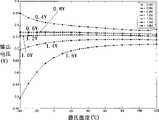
图3是本发明提供的自偏置运算跨导放大器随温度和工艺转角变化的环路增益曲线;其中,输入小信号幅度归一到1V,a=0.9;Fig. 3 is the loop gain curve of the self-biased operational transconductance amplifier provided by the present invention as the temperature and process corner change; wherein, the input small signal amplitude is normalized to 1V, a=0.9;
图4是本发明提供的自偏置运算跨导放大器随温度和电源电压的环路增益曲线;其中,输入小信号幅度归一到1V;Fig. 4 is the loop gain curve of the self-biased operational transconductance amplifier provided by the present invention with temperature and power supply voltage; wherein, the amplitude of the input small signal is normalized to 1V;
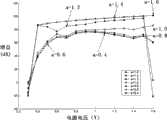
图5是本发明提供的自偏置运算跨导放大器随电源电压和环路增益控制参数a变化的开环增益曲线;其中,输入小信号幅度归一到1V。Fig. 5 is the open-loop gain curve of the self-biased operational transconductance amplifier provided by the present invention as the power supply voltage and loop gain control parameter a change; wherein, the amplitude of the input small signal is normalized to 1V.
具体实施方式Detailed ways
为使本发明的目的、技术方案和优点更加清楚明白,以下结合具体实施例,并参照附图,对本发明进一步详细说明。In order to make the object, technical solution and advantages of the present invention clearer, the present invention will be described in further detail below in conjunction with specific embodiments and with reference to the accompanying drawings.
如图1所示,图1是本发明提供的自偏置运算跨导放大器的电路图,该电路由一偏置电路11、一差分输入级电路12、一输出级电路13和一两级放大器补偿电路14构成。As shown in Figure 1, Figure 1 is a circuit diagram of a self-biased operational transconductance amplifier provided by the present invention, which is compensated by a
其中,所述偏置电路11包括PMOS晶体管PM0和PM1,以及NMOS晶体管NM0和NM1;其中,NM1的栅级、NM0的栅级和漏级以及PM0的漏级直接耦合,PM1的栅级和漏级、NM1的漏级与所述差分输入级电路12中PM2、PM3的栅级直接耦合,PM0和PM1的源级与参考电源相连接,NM0和NM1的源级与参考地相连接。Wherein, the
偏置电路11提供差分输入级电路12的直流偏置,使得差分输入级电路12可以提供足够高的小信号增益,输入小信号经差分输入级电路12放大,输出信号经输出级电路13被进一步的放大且提供了较低的输出阻抗,而偏置电路11的直流偏置则由输出级电路13提供,这样形成了一个自偏置的运算跨导放大器,为了控制环路增益并且降低电路功耗,所述偏置电路11提供了一个电流增益k。The
所述差分输入级电路12包括NMOS晶体管NM2、NM3、NM5和NM6,以及PMOS晶体管PM2和PM3;其中PM2和PM3的栅级与所述偏置电路11中PM1的栅级直接相连接,漏级分别与NM2、NM3的漏级相连接,源级与参考电源相连接;NMOS管NM2和NM3的栅级为所述自偏置低压运算跨导放大器电路的差分输入端口,漏级分别与PM2和PM3的漏级以及NM5和NM6的栅级相连接,同时,NM3的漏级还与所述两级放大器补偿电路14的电阻一端相连接;NM2和NM3的源级以及NM5和NM6的漏级直接耦合。The differential
所述NMOS晶体管NM5和NM6为尾电流管,该尾电流管NM5和NM6为所述差分输入级电路12提供直流偏置电流。尾电流管NM5和NM6的漏极分别与差分输入对NM2和NM3的源极相连,栅极分别与NM2和NM3的漏极相连,该结构提供了差分输入级电路12的共模反馈,当差分输入级电路12的输出共模信号增大时,控制尾电流也随之增大,然后共模反馈的负反馈机制开始工作,并促使输出共模电平降低,保证了电路的正常工作。The NMOS transistors NM5 and NM6 are tail current transistors, and the tail current transistors NM5 and NM6 provide a DC bias current for the differential
所述输出级电路13的输入管为NMOS晶体管NM4,栅级与NM3的漏级直接相连接;负载管为二极管形式连接的PMOS晶体管PM4,PM4的漏极与栅极以及NM4的漏级相连接,并耦合到所述偏置电路11中PM0的栅级,为偏置电路提供电流,PM4的源极与参考电源相连接,NM4的漏级与参考地相连接。所述输出级电路13为一简单的共源放大器,所述晶体管PM4为所述偏置电路11提供电流。所述输出级电路13几乎不提供电压增益,但它减小了输入阻抗,使设计的运算跨导放大器具有较大的驱动能力,同时它提供了从运算跨导放大器到偏置电路的电流增益。The input tube of the
所述两级放大器补偿电路14用于为所述偏置电路11的闭环相位裕度进行补偿,包括电阻R0和电容Cc,其中R0和Cc的一端直接相连接,R0的另一端与NM3的漏级相连接,Cc的另一端与NM4的漏级即放大器的输出端口相连接。补偿电路14采用传统的密勒电容以及串联的消零电阻对自偏置运算放大器的第二主极点和右半平面零点进行了补偿,为运算跨导放大器留出了充裕的相位裕度,一般将运算跨导放大器的相位裕度设置为60度左右,在阶跃响应和稳定性之间作一个较好的折衷,同时保证了电路的稳定工作。The two-stage
所述偏置电路11提供差分输入级电路12的直流偏置,使得差分输入级电路12提供足够高的小信号增益,输入小信号经差分输入级电路12放大,输出信号经输出级电路13被进一步放大且提供了较低的输出阻抗,而偏置电路11的直流偏置则由输出级电路13提供,形成一个自偏置的运算跨导放大器。The
下面对电路的结构作一详细分析。该电路形式类似于传统的两级运算跨导放大器结构,所不同的是其偏置电路提供的电流是由运算跨导放大器的输出级直接镜像,因此必须对该放大器的环路特性作分析。按照Behzad Razavi所著的《模拟CMOS集成电路设计》一书中所述,对该运算跨导放大器作小信号分析,即用小信号模型来代替所有的晶体管,从而得到电路的电气特性。The structure of the circuit is analyzed in detail below. The circuit form is similar to the traditional two-stage operational transconductance amplifier structure, the difference is that the current provided by the bias circuit is directly mirrored by the output stage of the operational transconductance amplifier, so the loop characteristics of the amplifier must be analyzed. According to the book "Analog CMOS Integrated Circuit Design" written by Behzad Razavi, the small signal analysis of the operational transconductance amplifier is performed, that is, the small signal model is used to replace all the transistors, so as to obtain the electrical characteristics of the circuit.
放大器的小信号模型如图2所示,如上图所示是放大器的小信号示意图,其中gm1是放大器输入管NM2,NM3的跨导,gm2是NM5,NM6的跨导,gm3是PM0的跨导,gm4是第二级输入管NM4的跨导,g4是第二级负载管PM4的跨导,R01、R02、R03分别是gm1、gm2、gm3的输出阻抗,为了使得下面的公式推导清晰明了,令g1,2,3=1/R01,02,03。将输入的差分信号vinn和vinp看成两个独立的信号驱动,因此可以用叠加法来计算输出。首先令vinp为零,然后求出Vinn对输出电压的影响。则由上面的示意图可得到下列的方程组:The small signal model of the amplifier is shown in Figure 2. The above figure is the small signal schematic diagram of the amplifier, where gm1 is the transconductance of the amplifier input tubes NM2 and NM3, gm2 is the transconductance of NM5 and NM6 , and gm3 is The transconductance of PM0, gm4 is the transconductance of the second-stage input tube NM4, g4 is the transconductance of the second-stage load tube PM4, R01 , R02 , and R03 are gm1 , gm2 , and gm3 respectively For the output impedance, in order to make the derivation of the following formula clear, set g1,2,3 =1/R01,02,03 . Consider the input differential signals vinn and vinp as two independent signal drivers, so the superposition method can be used to calculate the output. Let vinp be zero first, and then find out the effect ofVin on the output voltage. Then the following equations can be obtained from the schematic diagram above:
得到以下四式:Get the following four formulas:
gm1(Vinn-Vt)+g1(V1-Vt)+g3V1+k×gm3×Vout=0 (1)gm1 (Vinn -Vt )+g1 (V1 -Vt )+g3 V1 +k×gm3 ×Vout =0 (1)
gm1(0-Vt)+g1(V2-Vt)+g3V2+kgm3Vout=0 (2)gm1 (0-Vt )+g1 (V2 -Vt )+g3 V2 +kgm3 Vout =0 (2)
gm2(V1+V2)+g2Vt+g3(V1+V2)+2kgm3Vout=0 (3)gm2 (V1 +V2 )+g2 Vt +g3 (V1 +V2 )+2kgm3 Vout =0 (3)
g4×Vout+gm4×V2=0 (4)g4 ×Vout +gm4 ×V2 =0 (4)
其中k=(SPM2×SNM1)/(SPM1×SNM0)表示电流经过一系列复制的比例系数,S表示MOS管的宽长比,可以解得:Among them, k=(SPM2 ×SNM1 )/(SPM1 ×SNM0 ) represents the proportional coefficient of the current passing through a series of copies, and S represents the width-to-length ratio of the MOS tube, which can be solved as follows:
Vout/Vinn=(g3+gm2)/(2×(g3+gm2)+(g1+g3+k×A×gm3)/(g1+gm1)×g2+2×k×A×gm3) (5)Vout /Vinn =(g3 +gm2 )/(2×(g3 +gm2 )+(g1 +g3 +k×A×gm3 )/(g1 +gm1 )×g2 +2×k×A×gm3 ) (5)
由于g1,g2,g3远小于gm1,gm2,gm3,gm4,化简得到:Since g1 , g2 , g3 are much smaller than gm1 , gm2 , gm3 , gm4 , the simplification gives:
Vout/Vinn=-0.5×gm4×gm1/g4/(g1+g3)×(1-k×A×gm4×gm3/g4/gm2) (6)Vout /Vinn =-0.5×gm4 ×gm1 /g4 /(g1 +g3 )×(1-k×A×gm4 ×gm3 /g4 /gm2 ) (6)
同理可以求出Vinp对输出电压的影响:In the same way, the influence of Vinp on the output voltage can be obtained:
Vout/Vinp=-0.5×gm4×gm1/g4/(g1+g3)×(1-k×A×gm4×gm3/g4/gm2) (7)Vout /Vinp =-0.5×gm4 ×gm1 /g4 /(g1 +g3 )×(1-k×A×gm4 ×gm3 /g4 /gm2 ) (7)
由式(6)和(7)可以得到:From formulas (6) and (7), we can get:
Vout/(Vinp-Vinn)=-0.5×gm4×gm1/g4/(g1+g3)×(1-k×A×gm4×gm3/g4/gm2) (8)Vout /(Vinp -Vinn )=-0.5×gm4 ×gm1 /g4 /(g1 +g3 )×(1-k×A×gm4 ×gm3 /g4 /gm2 ) (8)
式(8)即为尾电流管相等时的小信号增益,可见,该增益表达式与传统的两级运算跨导放大器的表达式的区别在于其系数不同。Equation (8) is the small-signal gain when the tail current tubes are equal. It can be seen that the difference between this gain expression and the expression of the traditional two-stage operational transconductance amplifier lies in the different coefficients.
现在考虑当输入级电路(12)的尾电流管尺寸不同时,假设正输入端(即Vinn)下的尾电流管和负输入端(即Vinp)的尺寸分别为a×S和S,则有增益表达式如下:Now consider when the sizes of the tail current tubes of the input stage circuit (12) are different, assuming that the size of the tail current tube under the positive input terminal (ie Vinn ) and the negative input terminal (ie Vinp ) are a×S and S respectively, Then the gain expression is as follows:
A=-0.5×gmNM2×gmNM4/(g0,NM2+g0,PM2)/gmPM4/(1-(SPM2,3×SNM1)/(SPM1×SNM0)×gmNM4×gmPM0/(gmPM4×gmNM5)) (9)A=-0.5×gmNM2 ×gmNM4 /(g0, NM2 +g0, PM2 )/gmPM4 /(1-(SPM2, 3 ×SNM1 )/(SPM1 ×SNM0 )×gmNM4 × gmPM0 /(gmPM4 ×gmNM5 )) (9)
由于上式较为复杂,可以将上式变换如下:Since the above formula is more complicated, the above formula can be transformed as follows:
A=0.5×A0/(1-(1+a)/(1+SQRT(a))) (10)A=0.5×A0 /(1-(1+a)/(1+SQRT(a))) (10)
其中,A0为差分输入级(12)和输入级(13)的开环增益之和,SQRT()为平方根运算函数。由于设计的运算跨导放大器为自偏置,该放大器存在三个环路:输入级的差分输入管加上漏端到尾电流源NMOS管栅极的共模反馈电路构成了前两个负反馈环路;而第三个环路则包括输出电压反馈到PM0后,经过偏置电路再经负载管PM3和输出级回到出发点,经过分析这个环路是正反馈。增益大于1的正反馈会导致电路的不稳定乃至振荡,因此,我们必须保证该反馈的环路增益小于1。Among them, A0 is the sum of the open-loop gains of the differential input stage (12) and the input stage (13), and SQRT() is a square root operation function. Since the designed operational transconductance amplifier is self-biased, there are three loops in the amplifier: the differential input transistor of the input stage plus the common-mode feedback circuit from the drain to the gate of the tail current source NMOS transistor constitutes the first two negative feedback circuits Loop; and the third loop includes output voltage feedback to PM0, after passing through the bias circuit and then returning to the starting point through the load tube PM3 and the output stage, this loop is positive feedback after analysis. Positive feedback with a gain greater than 1 will lead to instability and even oscillation of the circuit, so we must ensure that the loop gain of the feedback is less than 1.
环路增益(loop gain,以下简称af)的计算一般以下面的方法进行。将放大器的输入小信号置零,在某点断开环路,在偏置点(PM0的栅极)注入一个测试小信号,使得信号沿环路直到另外一个断点(即输出级的输出点),我们得到一个电压值。这样导出的传输函数的负值就是环路增益T,采用af法得到的环路增益表达式如下所示:The loop gain (loop gain, hereinafter referred to as af) is generally calculated in the following manner. Set the input small signal of the amplifier to zero, break the loop at a certain point, and inject a small test signal at the bias point (the gate of PM0), so that the signal goes along the loop until another breakpoint (that is, the output point of the output stage) ), we get a voltage value. The negative value of the transfer function derived in this way is the loop gain T, and the expression of the loop gain obtained by using the af method is as follows:
T=(1+a)/(1+SQRT(a)) (11)T=(1+a)/(1+SQRT(a)) (11)
将(11)式带入(10)式,可得:Put (11) into (10), we can get:
A=0.5×A0/(1-T) (12)A=0.5×A0 /(1-T) (12)
由式(12)可见,设计的运算放大器的开环增益取决于其自偏置结构的环路增益,当a等于1时,环路增益T等于1,此时运算跨导放大器的开环增益为无穷大,当a从1向着零的方向减小时,所述放大器的开环增益也随之减小,而当a趋近于0时,所述环路增益为0,同时放大器的开环增益等于传统两级跨导放大器增益的一半。可见,环路增益的选择影响了电路的开环增益。It can be seen from formula (12) that the open-loop gain of the designed operational amplifier depends on the loop gain of its self-bias structure. When a is equal to 1, the loop gain T is equal to 1. At this time, the open-loop gain of the operational transconductance amplifier is infinite, when a decreases from 1 to zero, the open-loop gain of the amplifier also decreases, and when a approaches 0, the loop gain is 0, and the open-loop gain of the amplifier It is equal to half of the gain of the traditional two-stage transconductance amplifier. It can be seen that the choice of loop gain affects the open loop gain of the circuit.
而由于工艺的浮动为一随机过程,为了留出充足的设计裕度,就必须将环路增益控制在1以下,而且环路增益越小则电路的稳定性也越好,但是随之而来的是电路开环增益乃至性能的下降。Since the fluctuation of the process is a random process, in order to leave sufficient design margin, the loop gain must be controlled below 1, and the smaller the loop gain, the better the stability of the circuit. The most important thing is the decrease of circuit open-loop gain and even performance.
由图3所示,所述的环路增益可控的自偏置运算跨导放大器的环路增益随温度和工艺转角变化曲线图,从图中可以看出,当尾电流管的尺寸之比a等于0.9时,在不同的温度和工艺转角下,所述放大器的环路增益稳定在0.75左右。As shown in Fig. 3, the loop gain of the self-biased operational transconductance amplifier with controllable loop gain varies with temperature and process angle curve, as can be seen from the figure, when the ratio of the size of the tail current tube When a is equal to 0.9, the loop gain of the amplifier is stable at about 0.75 under different temperatures and process corners.
由图4所示,所述的自偏置运算跨导放大器随温度和电源电压的环路增益曲线,当尾电流管的尺寸之比a等于0.9时,在不同的温度和电源电压下,所述放大器的环路增益同样稳定在0.75左右。As shown in Figure 4, the loop gain curve of the self-biased operational transconductance amplifier with temperature and power supply voltage, when the ratio a of the size of the tail current tube is equal to 0.9, under different temperatures and power supply voltages, the The loop gain of the above amplifier is also stable at about 0.75.
由图4和图5可以看出,所述放大器电路的环路增益不随温度、工艺转角和电源电压的变换而变化,保证了当环路增益可控时电路的稳定。It can be seen from FIG. 4 and FIG. 5 that the loop gain of the amplifier circuit does not change with changes in temperature, process corner and power supply voltage, which ensures the stability of the circuit when the loop gain is controllable.
自偏置运算跨导放大器随电源电压和环路增益控制参数a变化的开环增益曲线,从图中可以看出,当a从1向0的方向逐渐减小时,电路的环路增益也随着减小,同时所述放大器的开环增益增大。The open-loop gain curve of the self-biased operational transconductance amplifier varies with the power supply voltage and the loop gain control parameter a. It can be seen from the figure that when a gradually decreases from 1 to 0, the loop gain of the circuit also changes with decreases while the open-loop gain of the amplifier increases.
由于控制尾电流管尺寸之比,可能会增加所述运算跨导放大器的输入失调电压,在仿真时采用蒙特卡罗分析对所述放大器的失调电压进行了分析和仿真,证明在低功耗设计时所述环路增益控制对放大器的输入失调电压影响可以忽略不计。Due to controlling the ratio of the size of the tail current tube, the input offset voltage of the operational transconductance amplifier may be increased. In the simulation, the offset voltage of the amplifier is analyzed and simulated by Monte Carlo analysis, which proves that the low power consumption design When the loop gain control has a negligible effect on the input offset voltage of the amplifier.
通过文献《王晗,叶青,0.6V电源电压的CMOS基准源设计及稳定性分析,半导体学报,第27卷,2006年8月,第1508页至第1513页》中采用本发明的该环路增益可控的自偏置运算跨导放大器设计流程,将尾电流管的尺寸之比a设置为0.95,采用SMIC 0.18umCMOS混合信号工艺实现的运算跨导放大器可以工作在0.4V的电源电压下,当电源电压为0.5V时所述运算跨导放大器的直流增益为58dB,单位增益带宽为13.5kHz,功耗为85nW。芯片流片的结果验证了该流程的正确性。The ring of the present invention is adopted in the document "Wang Han, Ye Qing, CMOS Reference Source Design and Stability Analysis of 0.6V Power Supply Voltage, Journal of Semiconductors, Volume 27, August 2006, Pages 1508 to 1513" The design process of a self-biased operational transconductance amplifier with controllable gain, the size ratio a of the tail current tube is set to 0.95, and the operational transconductance amplifier realized by SMIC 0.18um CMOS mixed-signal technology can work at a power supply voltage of 0.4V , when the power supply voltage is 0.5V, the DC gain of the operational transconductance amplifier is 58dB, the unity gain bandwidth is 13.5kHz, and the power consumption is 85nW. The results of the chip tape-out verified the correctness of the process.
因此本发明的运算跨导放大器可以通过对参数a的控制,从而达到灵活的控制其环路增益的目的。根据不同的工艺和设计要求,所述运算跨导放大器可以将电路的环路增益设置在稳定性考虑的范围边缘,从而使电路的性能达到最优。Therefore, the operational transconductance amplifier of the present invention can flexibly control its loop gain by controlling the parameter a. According to different process and design requirements, the operational transconductance amplifier can set the loop gain of the circuit at the edge of the range considered for stability, so that the performance of the circuit can be optimized.
至此,可以理解,本发明提供的这种环路增益可控的运算跨导放大器电路,采用自偏置的运算跨导放大器来提供两级运算跨导放大器的直流偏置,同时为运算跨导放大器电路提供部分正反馈机制,通过对差分输入级尾电流管尺寸的比例来控制其环路增益,从而在电路稳定性和性能之间得到最优的折衷。So far, it can be understood that the operational transconductance amplifier circuit with controllable loop gain provided by the present invention adopts a self-biased operational transconductance amplifier to provide the DC bias of the two-stage operational transconductance amplifier, and simultaneously provides the operational transconductance amplifier The amplifier circuit provides a partial positive feedback mechanism to control its loop gain through the ratio of the size of the tail current tube of the differential input stage, so as to obtain an optimal trade-off between circuit stability and performance.
基于本发明的这种环路增益可控的运算跨导放大器电路,本发明还提供了一种实现自偏置运算跨导放大器电路的环路增益控制方法,该方法包括:Based on the operational transconductance amplifier circuit with controllable loop gain of the present invention, the present invention also provides a loop gain control method for realizing a self-bias operational transconductance amplifier circuit, the method comprising:
设计差分输入级电路,负载电流镜所需的偏置电流由理想电流源产生,同时设计尺寸相同的尾电流管NM5和NM6,使得差分输入级能够提供一定的增益并且为第二级输出级电路提供直流偏置点,同时按照上述结构设计可以为差分输入级提供一定的共模反馈;Design a differential input stage circuit. The bias current required by the load current mirror is generated by an ideal current source. At the same time, design tail current transistors NM5 and NM6 with the same size, so that the differential input stage can provide a certain gain and provide a certain gain for the second stage output stage circuit. Provide a DC bias point, and at the same time provide a certain common-mode feedback for the differential input stage according to the above-mentioned structural design;
设计输出级电路,使两级运算跨导放大器能够提供足够的小信号增益;Design the output stage circuit so that the two-stage operational transconductance amplifier can provide sufficient small-signal gain;
选择合适的电阻和电容使得开环形式下的运算跨导放大器能够提供充裕的相位裕度;Selecting the appropriate resistors and capacitors enables the operational transconductance amplifier in the open-loop form to provide sufficient phase margin;
将偏置电路中的理想电流源用输出级的负载管来代替,形成一个环路,由于共模反馈的存在该电路能够稳定工作;The ideal current source in the bias circuit is replaced by the load tube of the output stage to form a loop, and the circuit can work stably due to the existence of common mode feedback;
调整补偿电路中的电阻和电容,使得环路形式下的运算跨导放大器具有足够的相位裕度;Adjust the resistance and capacitance in the compensation circuit so that the operational transconductance amplifier in the loop form has sufficient phase margin;
调整差分输入级中尾电流管尺寸例,同时也改变运放的环路增益和开环增益。Adjusting the size of the tail current tube in the differential input stage also changes the loop gain and open-loop gain of the op amp.
该控制方法不同于一般的开环运算放大器设计流程,所述的自偏置运算跨导放大器的偏置电流是由自身输出级电路提供的,所述自偏置运算跨导放大器在内部形成了一个环路结构,通过调整差分输入级电路的尾电流管尺寸的比值可以选择适当的环路增益来满足不同的设计要求。This control method is different from the general open-loop operational amplifier design process. The bias current of the self-biased operational transconductance amplifier is provided by its own output stage circuit, and the self-biased operational transconductance amplifier is internally formed. A loop structure, by adjusting the ratio of the size of the tail current tube of the differential input stage circuit, an appropriate loop gain can be selected to meet different design requirements.
该电路为无需外部基准电流源的自偏置运算跨导放大器,其负载需要的直流电流由运算跨导放大器本身提供,自偏置电路在运算跨导放大器内部形成了环路。The circuit is a self-biased operational transconductance amplifier that does not need an external reference current source. The DC current required by the load is provided by the operational transconductance amplifier itself. The self-bias circuit forms a loop inside the operational transconductance amplifier.
以上所述的具体实施例,对本发明的目的、技术方案和有益效果进行了进一步详细说明,所应理解的是,以上所述仅为本发明的具体实施例而已,并不用于限制本发明,凡在本发明的精神和原则之内,所做的任何修改、等同替换、改进等,均应包含在本发明的保护范围之内。The specific embodiments described above have further described the purpose, technical solutions and beneficial effects of the present invention in detail. It should be understood that the above descriptions are only specific embodiments of the present invention and are not intended to limit the present invention. Any modifications, equivalent replacements, improvements, etc. made within the spirit and principles of the present invention shall be included within the protection scope of the present invention.
Claims (10)
Translated fromChinesePriority Applications (1)
| Application Number | Priority Date | Filing Date | Title |
|---|---|---|---|
| CN2007103038903ACN101471632B (en) | 2007-12-26 | 2007-12-26 | Self-biased low-voltage operational transconductance amplifier circuit with controllable loop gain |
Applications Claiming Priority (1)
| Application Number | Priority Date | Filing Date | Title |
|---|---|---|---|
| CN2007103038903ACN101471632B (en) | 2007-12-26 | 2007-12-26 | Self-biased low-voltage operational transconductance amplifier circuit with controllable loop gain |
Publications (2)
| Publication Number | Publication Date |
|---|---|
| CN101471632Atrue CN101471632A (en) | 2009-07-01 |
| CN101471632B CN101471632B (en) | 2011-07-20 |
Family
ID=40828805
Family Applications (1)
| Application Number | Title | Priority Date | Filing Date |
|---|---|---|---|
| CN2007103038903AExpired - Fee RelatedCN101471632B (en) | 2007-12-26 | 2007-12-26 | Self-biased low-voltage operational transconductance amplifier circuit with controllable loop gain |
Country Status (1)
| Country | Link |
|---|---|
| CN (1) | CN101471632B (en) |
Cited By (21)
| Publication number | Priority date | Publication date | Assignee | Title |
|---|---|---|---|---|
| CN101588164B (en)* | 2009-06-18 | 2010-11-10 | 中国科学院微电子研究所 | Constant transconductance biasing circuit |
| CN102006022A (en)* | 2010-12-09 | 2011-04-06 | 中国电子科技集团公司第二十四研究所 | Low voltage operational amplifier based on CMOS (complementary metal oxide semiconductor) process |
| CN102158188A (en)* | 2011-03-15 | 2011-08-17 | 清华大学 | Low-power consumption bandwidth-multiplying operational amplifier realized by metal oxide semiconductor (MOS) devices |
| CN102215028A (en)* | 2010-04-06 | 2011-10-12 | 联发科技股份有限公司 | amplifier |
| CN104467709A (en)* | 2013-09-19 | 2015-03-25 | 美国亚德诺半导体公司 | Current-feedback operational amplifier |
| CN104796092A (en)* | 2014-01-22 | 2015-07-22 | 上海华虹集成电路有限责任公司 | An equalization circuit |
| CN105024663A (en)* | 2014-04-18 | 2015-11-04 | 清华大学 | Transconductance amplifier and high-robustness mixer circuit |
| CN106301264A (en)* | 2016-08-12 | 2017-01-04 | 中国科学院上海高等研究院 | A kind of Slew Rate enhancement mode operational amplifier |
| CN106452381A (en)* | 2016-12-05 | 2017-02-22 | 福州大学 | Coupling-capacitance-free instrument amplifier with direct current offset inhibition function and implementation method thereof |
| CN106685359A (en)* | 2016-11-11 | 2017-05-17 | 合肥兆芯电子有限公司 | Clock signal generating circuit, memory storage device and clock signal generating method |
| CN107078704A (en)* | 2014-07-02 | 2017-08-18 | 罗伯特·博世有限公司 | Adjusting means for trsanscondutance amplifier |
| CN107210716A (en)* | 2015-01-12 | 2017-09-26 | 高通股份有限公司 | For calibrating the method and apparatus that mutual conductance or gain change with technique or condition in difference channel |
| CN108008933A (en)* | 2016-11-02 | 2018-05-08 | 中芯国际集成电路制造(上海)有限公司 | A kind of circuit of random sequence number for being used to produce chip and the chip including the circuit |
| CN108121391A (en)* | 2016-11-29 | 2018-06-05 | 意法半导体(格勒诺布尔2)公司 | For carrying out the method and apparatus of automatic biasing and the common mode amplification that is self-regulated |
| CN109546975A (en)* | 2019-01-29 | 2019-03-29 | 苏州大学 | Operation transconductance amplifier |
| CN110047451A (en)* | 2019-04-09 | 2019-07-23 | 深圳市华星光电半导体显示技术有限公司 | Source electrode driver, array substrate and liquid crystal display panel |
| CN110739923A (en)* | 2018-07-19 | 2020-01-31 | 江苏润石科技有限公司 | Operational amplifier circuit |
| CN111541433A (en)* | 2020-05-26 | 2020-08-14 | 哈尔滨工业大学 | A transconductance operational amplifier circuit and filter circuit |
| WO2021174797A1 (en)* | 2020-03-06 | 2021-09-10 | 锐石创芯(深圳)科技有限公司 | Power supply network capable of switching loop gains, signal processing system, and application |
| CN114065685A (en)* | 2021-11-23 | 2022-02-18 | 中国核动力研究设计院 | Gain circuit construction method and system, electronic device and storage medium |
| WO2024012453A1 (en)* | 2022-07-12 | 2024-01-18 | 北京集创北方科技股份有限公司 | Driving circuit, display driving chip, display device, and electronic device |
Family Cites Families (5)
| Publication number | Priority date | Publication date | Assignee | Title |
|---|---|---|---|---|
| US4731589A (en)* | 1986-07-25 | 1988-03-15 | Rca Corporation | Constant current load and level shifter circuitry |
| JPH05191162A (en)* | 1991-09-18 | 1993-07-30 | Hitachi Ltd | Operational amplifier and line terminating device |
| US6407623B1 (en)* | 2001-01-31 | 2002-06-18 | Qualcomm Incorporated | Bias circuit for maintaining a constant value of transconductance divided by load capacitance |
| JP3520418B2 (en)* | 2002-02-04 | 2004-04-19 | セイコーエプソン株式会社 | Operational amplifier circuit, drive circuit, and control method of operational amplifier circuit |
| KR100620662B1 (en)* | 2003-09-26 | 2006-09-19 | 엔이씨 일렉트로닉스 가부시키가이샤 | Differential ab class amplifier circuit and drive circuit using the same |
- 2007
- 2007-12-26CNCN2007103038903Apatent/CN101471632B/ennot_activeExpired - Fee Related
Cited By (32)
| Publication number | Priority date | Publication date | Assignee | Title |
|---|---|---|---|---|
| CN101588164B (en)* | 2009-06-18 | 2010-11-10 | 中国科学院微电子研究所 | Constant transconductance biasing circuit |
| CN102215028A (en)* | 2010-04-06 | 2011-10-12 | 联发科技股份有限公司 | amplifier |
| CN102215028B (en)* | 2010-04-06 | 2013-11-06 | 联发科技股份有限公司 | amplifier |
| CN102006022A (en)* | 2010-12-09 | 2011-04-06 | 中国电子科技集团公司第二十四研究所 | Low voltage operational amplifier based on CMOS (complementary metal oxide semiconductor) process |
| CN102006022B (en)* | 2010-12-09 | 2014-04-16 | 中国电子科技集团公司第二十四研究所 | Low voltage operational amplifier based on CMOS (complementary metal oxide semiconductor) process |
| CN102158188A (en)* | 2011-03-15 | 2011-08-17 | 清华大学 | Low-power consumption bandwidth-multiplying operational amplifier realized by metal oxide semiconductor (MOS) devices |
| CN102158188B (en)* | 2011-03-15 | 2013-02-27 | 清华大学 | Low Power Bandwidth Doubler Operational Amplifier Implemented Using MOS Devices |
| CN104467709A (en)* | 2013-09-19 | 2015-03-25 | 美国亚德诺半导体公司 | Current-feedback operational amplifier |
| CN104467709B (en)* | 2013-09-19 | 2018-06-08 | 美国亚德诺半导体公司 | Operating amplifier with current feedback |
| CN104796092B (en)* | 2014-01-22 | 2018-02-13 | 上海华虹集成电路有限责任公司 | Equalizing circuit |
| CN104796092A (en)* | 2014-01-22 | 2015-07-22 | 上海华虹集成电路有限责任公司 | An equalization circuit |
| CN105024663A (en)* | 2014-04-18 | 2015-11-04 | 清华大学 | Transconductance amplifier and high-robustness mixer circuit |
| CN105024663B (en)* | 2014-04-18 | 2017-11-24 | 清华大学 | A kind of trsanscondutance amplifier and high robust mixer |
| CN107078704B (en)* | 2014-07-02 | 2020-06-16 | 罗伯特·博世有限公司 | Adjusting device for transconductance amplifier |
| CN107078704A (en)* | 2014-07-02 | 2017-08-18 | 罗伯特·博世有限公司 | Adjusting means for trsanscondutance amplifier |
| CN107210716A (en)* | 2015-01-12 | 2017-09-26 | 高通股份有限公司 | For calibrating the method and apparatus that mutual conductance or gain change with technique or condition in difference channel |
| CN106301264B (en)* | 2016-08-12 | 2019-04-16 | 中国科学院上海高等研究院 | A kind of enhanced operational amplifier of Slew Rate |
| CN106301264A (en)* | 2016-08-12 | 2017-01-04 | 中国科学院上海高等研究院 | A kind of Slew Rate enhancement mode operational amplifier |
| CN108008933A (en)* | 2016-11-02 | 2018-05-08 | 中芯国际集成电路制造(上海)有限公司 | A kind of circuit of random sequence number for being used to produce chip and the chip including the circuit |
| CN108008933B (en)* | 2016-11-02 | 2022-02-08 | 中芯国际集成电路制造(上海)有限公司 | Circuit for generating random serial number of chip and chip comprising same |
| CN106685359A (en)* | 2016-11-11 | 2017-05-17 | 合肥兆芯电子有限公司 | Clock signal generating circuit, memory storage device and clock signal generating method |
| CN108121391A (en)* | 2016-11-29 | 2018-06-05 | 意法半导体(格勒诺布尔2)公司 | For carrying out the method and apparatus of automatic biasing and the common mode amplification that is self-regulated |
| CN106452381A (en)* | 2016-12-05 | 2017-02-22 | 福州大学 | Coupling-capacitance-free instrument amplifier with direct current offset inhibition function and implementation method thereof |
| CN106452381B (en)* | 2016-12-05 | 2023-03-14 | 福州大学 | Instrument amplifier with direct current offset suppression function and implementation method thereof |
| CN110739923A (en)* | 2018-07-19 | 2020-01-31 | 江苏润石科技有限公司 | Operational amplifier circuit |
| CN109546975A (en)* | 2019-01-29 | 2019-03-29 | 苏州大学 | Operation transconductance amplifier |
| CN109546975B (en)* | 2019-01-29 | 2023-09-29 | 苏州大学 | operational transconductance amplifier |
| CN110047451A (en)* | 2019-04-09 | 2019-07-23 | 深圳市华星光电半导体显示技术有限公司 | Source electrode driver, array substrate and liquid crystal display panel |
| WO2021174797A1 (en)* | 2020-03-06 | 2021-09-10 | 锐石创芯(深圳)科技有限公司 | Power supply network capable of switching loop gains, signal processing system, and application |
| CN111541433A (en)* | 2020-05-26 | 2020-08-14 | 哈尔滨工业大学 | A transconductance operational amplifier circuit and filter circuit |
| CN114065685A (en)* | 2021-11-23 | 2022-02-18 | 中国核动力研究设计院 | Gain circuit construction method and system, electronic device and storage medium |
| WO2024012453A1 (en)* | 2022-07-12 | 2024-01-18 | 北京集创北方科技股份有限公司 | Driving circuit, display driving chip, display device, and electronic device |
Also Published As
| Publication number | Publication date |
|---|---|
| CN101471632B (en) | 2011-07-20 |
Similar Documents
| Publication | Publication Date | Title |
|---|---|---|
| CN101471632B (en) | Self-biased low-voltage operational transconductance amplifier circuit with controllable loop gain | |
| CN101339443B (en) | Broad output current scope low pressure difference linear manostat | |
| CN102045035B (en) | A low-power, wideband, high-gain, high-slew-rate single-stage operational transconductance amplifier | |
| CN204679894U (en) | A kind of CMOS low temperature low noise discharge circuit | |
| CN101355346B (en) | Frequency Compensation Method of Broadband Common Mode Feedback Loop for Two-Stage Operational Amplifier | |
| CN100549898C (en) | Utilize two-way asymmetric buffer structure to improve the LDO circuit of performance | |
| KR102415919B1 (en) | Inverting Pseudo-Full Differential Amplifier With Common Mode Feedback Control Circuit | |
| CN101917168B (en) | High Slew Rate Transconductance Amplifier Used in Active Power Factor Correctors | |
| CN103546127A (en) | A low-power high-speed comparator with offset storage | |
| CN101916128B (en) | Method and corresponding circuit for improving output power supply rejection ratio of band-gap reference source | |
| CN107422774B (en) | A kind of on piece LDO of low pressure fast transient response | |
| CN101217279A (en) | A Low Power Comparator with Offset Calibration | |
| CN101951236A (en) | Digital variable gain amplifier | |
| CN103095231B (en) | A kind of common mode feedback circuit | |
| CN101839941B (en) | Signal sensing amplifier | |
| CN110212866A (en) | A kind of low-power consumption three-stage operational amplifier driving heavy load capacitor | |
| CN115395906B (en) | A low-power broadband common-mode signal detection circuit suitable for ultra-low voltage | |
| CN103414438A (en) | Error amplifier circuit | |
| CN109546975A (en) | Operation transconductance amplifier | |
| CN110798203A (en) | High Linearity Unity Gain Voltage Buffer in Nanoscale CMOS Process | |
| CN118449464A (en) | A low noise and low offset rail-to-rail operational amplifier based on BCD technology | |
| CN102355212A (en) | Rail-to-rail input stage with current compensation function | |
| CN101098123A (en) | A low-voltage and low-power pseudo-two-stage Class-AB OTA structure | |
| CN114598273B (en) | All-SiC CMOS operational amplifier with temperature stability | |
| CN102609028B (en) | Phase compensation controller |
Legal Events
| Date | Code | Title | Description |
|---|---|---|---|
| C06 | Publication | ||
| PB01 | Publication | ||
| C10 | Entry into substantive examination | ||
| SE01 | Entry into force of request for substantive examination | ||
| C14 | Grant of patent or utility model | ||
| GR01 | Patent grant | ||
| C41 | Transfer of patent application or patent right or utility model | ||
| TR01 | Transfer of patent right | Effective date of registration:20161031 Address after:100176, No. 10, Ronghua Road, Beijing economic and Technological Development Zone, 9 floor, block A Patentee after:BRITE SEMICONDUCTOR, Inc. Address before:100029 Beijing city Chaoyang District Beitucheng West Road No. 3 Patentee before:Institute of Microelectronics of the Chinese Academy of Sciences | |
| CF01 | Termination of patent right due to non-payment of annual fee | Granted publication date:20110720 | |
| CF01 | Termination of patent right due to non-payment of annual fee |