CN101465341A - Stacked chip packaging structure - Google Patents
Stacked chip packaging structureDownload PDFInfo
- Publication number
- CN101465341A CN101465341ACNA2007101601848ACN200710160184ACN101465341ACN 101465341 ACN101465341 ACN 101465341ACN A2007101601848 ACNA2007101601848 ACN A2007101601848ACN 200710160184 ACN200710160184 ACN 200710160184ACN 101465341 ACN101465341 ACN 101465341A
- Authority
- CN
- China
- Prior art keywords
- those
- chips
- packaging structure
- chip packaging
- layer
- Prior art date
- Legal status (The legal status is an assumption and is not a legal conclusion. Google has not performed a legal analysis and makes no representation as to the accuracy of the status listed.)
- Granted
Links
- 238000004806packaging method and processMethods0.000titleclaimsabstractdescription44
- 239000000758substrateSubstances0.000claimsabstractdescription54
- 238000007789sealingMethods0.000claimsdescription2
- 239000010410layerSubstances0.000description94
- 229910000679solderInorganic materials0.000description17
- 238000004519manufacturing processMethods0.000description11
- 229910052710siliconInorganic materials0.000description8
- 239000010703siliconSubstances0.000description8
- XUIMIQQOPSSXEZ-UHFFFAOYSA-NSiliconChemical compound[Si]XUIMIQQOPSSXEZ-UHFFFAOYSA-N0.000description6
- 239000004020conductorSubstances0.000description6
- PCHJSUWPFVWCPO-UHFFFAOYSA-NgoldChemical compound[Au]PCHJSUWPFVWCPO-UHFFFAOYSA-N0.000description6
- 238000000034methodMethods0.000description6
- 238000003860storageMethods0.000description6
- 239000000565sealantSubstances0.000description5
- 238000010586diagramMethods0.000description4
- 239000008393encapsulating agentSubstances0.000description4
- 239000010931goldSubstances0.000description4
- 229910052737goldInorganic materials0.000description4
- 239000000463materialSubstances0.000description4
- 238000012536packaging technologyMethods0.000description4
- 239000012790adhesive layerSubstances0.000description2
- 230000002411adverseEffects0.000description2
- 238000005516engineering processMethods0.000description2
- 239000007788liquidSubstances0.000description2
- 238000003466weldingMethods0.000description2
- 239000004642PolyimideSubstances0.000description1
- 239000003822epoxy resinSubstances0.000description1
- 238000005530etchingMethods0.000description1
- 239000003292glueSubstances0.000description1
- 238000012986modificationMethods0.000description1
- 230000004048modificationEffects0.000description1
- 231100000989no adverse effectToxicity0.000description1
- 238000012858packaging processMethods0.000description1
- 230000002093peripheral effectEffects0.000description1
- 238000000206photolithographyMethods0.000description1
- 229920000647polyepoxidePolymers0.000description1
- 229920001721polyimidePolymers0.000description1
- 239000004065semiconductorSubstances0.000description1
Images


Classifications
- H—ELECTRICITY
- H01—ELECTRIC ELEMENTS
- H01L—SEMICONDUCTOR DEVICES NOT COVERED BY CLASS H10
- H01L2224/00—Indexing scheme for arrangements for connecting or disconnecting semiconductor or solid-state bodies and methods related thereto as covered by H01L24/00
- H01L2224/01—Means for bonding being attached to, or being formed on, the surface to be connected, e.g. chip-to-package, die-attach, "first-level" interconnects; Manufacturing methods related thereto
- H01L2224/26—Layer connectors, e.g. plate connectors, solder or adhesive layers; Manufacturing methods related thereto
- H01L2224/31—Structure, shape, material or disposition of the layer connectors after the connecting process
- H01L2224/32—Structure, shape, material or disposition of the layer connectors after the connecting process of an individual layer connector
- H01L2224/321—Disposition
- H01L2224/32135—Disposition the layer connector connecting between different semiconductor or solid-state bodies, i.e. chip-to-chip
- H01L2224/32145—Disposition the layer connector connecting between different semiconductor or solid-state bodies, i.e. chip-to-chip the bodies being stacked
- H—ELECTRICITY
- H01—ELECTRIC ELEMENTS
- H01L—SEMICONDUCTOR DEVICES NOT COVERED BY CLASS H10
- H01L2224/00—Indexing scheme for arrangements for connecting or disconnecting semiconductor or solid-state bodies and methods related thereto as covered by H01L24/00
- H01L2224/73—Means for bonding being of different types provided for in two or more of groups H01L2224/10, H01L2224/18, H01L2224/26, H01L2224/34, H01L2224/42, H01L2224/50, H01L2224/63, H01L2224/71
- H01L2224/732—Location after the connecting process
- H01L2224/73251—Location after the connecting process on different surfaces
- H01L2224/73265—Layer and wire connectors
- H—ELECTRICITY
- H01—ELECTRIC ELEMENTS
- H01L—SEMICONDUCTOR DEVICES NOT COVERED BY CLASS H10
- H01L2224/00—Indexing scheme for arrangements for connecting or disconnecting semiconductor or solid-state bodies and methods related thereto as covered by H01L24/00
- H01L2224/80—Methods for connecting semiconductor or other solid state bodies using means for bonding being attached to, or being formed on, the surface to be connected
- H01L2224/85—Methods for connecting semiconductor or other solid state bodies using means for bonding being attached to, or being formed on, the surface to be connected using a wire connector
- H01L2224/85909—Post-treatment of the connector or wire bonding area
- H01L2224/8592—Applying permanent coating, e.g. protective coating
- H—ELECTRICITY
- H01—ELECTRIC ELEMENTS
- H01L—SEMICONDUCTOR DEVICES NOT COVERED BY CLASS H10
- H01L2924/00—Indexing scheme for arrangements or methods for connecting or disconnecting semiconductor or solid-state bodies as covered by H01L24/00
- H01L2924/15—Details of package parts other than the semiconductor or other solid state devices to be connected
- H01L2924/151—Die mounting substrate
- H01L2924/153—Connection portion
- H01L2924/1531—Connection portion the connection portion being formed only on the surface of the substrate opposite to the die mounting surface
- H01L2924/15311—Connection portion the connection portion being formed only on the surface of the substrate opposite to the die mounting surface being a ball array, e.g. BGA
- H—ELECTRICITY
- H01—ELECTRIC ELEMENTS
- H01L—SEMICONDUCTOR DEVICES NOT COVERED BY CLASS H10
- H01L2924/00—Indexing scheme for arrangements or methods for connecting or disconnecting semiconductor or solid-state bodies as covered by H01L24/00
- H01L2924/15—Details of package parts other than the semiconductor or other solid state devices to be connected
- H01L2924/181—Encapsulation
Landscapes
- Combinations Of Printed Boards (AREA)
Abstract
Description
Translated fromChinese技术领域technical field
本发明是有关于一种芯片封装结构,且特别是有关于一种堆叠式芯片封装结构及其制造方法。The present invention relates to a chip packaging structure, and in particular to a stacked chip packaging structure and a manufacturing method thereof.
背景技术Background technique
堆叠式芯片封装结构是利用三维封装技术将多个芯片垂直堆叠的半导体封装结构,可应用于存储器模组、记忆卡或随身碟等储存装置中。存储器模组是一种规格化的产品,例如是动态随机存取存储器(DRAM)模组,常用于桌上型电脑、笔记型电脑或工业用的电脑中,其存储容量和存取速度不断地加大、加快,以符合电脑运算的要求。现有的存储器模组是在单一电路板上设置多个存储器芯片,而这些存储器芯片以单面直排或双面直排的方式配置,并利用表面粘着技术(Surface Mount Technology,SMT)将其接脚焊接于基板上。此外,利用电路板上设置的插入式表面接合接口(例如金手指),存储器模组可插置于电脑的主机板的PCI插槽中,用以传输所需的资料。The stacked chip packaging structure is a semiconductor packaging structure in which multiple chips are vertically stacked using three-dimensional packaging technology, and can be applied to storage devices such as memory modules, memory cards, or flash drives. A memory module is a standardized product, such as a dynamic random access memory (DRAM) module, which is often used in desktop computers, notebook computers or industrial computers, and its storage capacity and access speed continue to increase. Increase and speed up to meet the requirements of computer computing. Existing memory modules are provided with multiple memory chips on a single circuit board, and these memory chips are configured in a single-sided in-line or double-sided in-line manner, and are mounted on them using Surface Mount Technology (SMT). The pins are soldered on the substrate. In addition, the memory module can be inserted into the PCI slot of the motherboard of the computer by using the plug-in surface-bonding interface (such as golden finger) provided on the circuit board to transmit required data.
然而,存储器模组的需求容量越大,相对地,存储器芯片的数量越高且基板所需的面积越大。因此,依照现有方式配置的存储器模组无法快速且大量的扩充其存储容量,势必朝三维封装结构发展。However, the larger the required capacity of the memory module, the higher the number of memory chips and the larger the required area of the substrate. Therefore, the memory module configured according to the existing method cannot rapidly and massively expand its storage capacity, and it is bound to develop into a three-dimensional packaging structure.
常见应用在存储器模组的封装技术,例如是打线接合(Wire bonding)封装、覆晶结合(Flip-chip bonding)封装、层叠式封装(Package On Package)、金凸块接合(Gold to Gold interconnection,GGI)封装以及硅穿孔(ThroughSilicon Via,TSV)封装等。这些封装技术都是为了满足高密度存储器容量的需求,而发展出来的三维封装结构。Common packaging technologies used in memory modules, such as wire bonding (Wire bonding) packaging, flip-chip bonding (Flip-chip bonding) packaging, stacked packaging (Package On Package), gold bump bonding (Gold to Gold interconnection) , GGI) package and through-silicon via (ThroughSilicon Via, TSV) package, etc. These packaging technologies are three-dimensional packaging structures developed to meet the demand for high-density memory capacity.
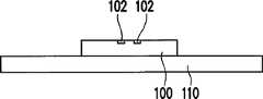
以硅穿孔封装技术为例,首先在硅基材上制作高深宽比的微通孔(Via),接着,填入一导电材料于微通孔中,并形成锡球(solder bump)于硅基材上,以使锡球与微通孔中的导电材料电性连接。请参考图1的堆叠式芯片封装结构,将多个芯片10依序堆叠且相邻二芯片10之间借由一粘着层40相隔。多个锡球30配置在相邻二芯片10之间,其与相邻微通孔12内的导电材料20电性连接,以达成芯片10之间的电性导通。然后,芯片10之间可再填入封胶50,以保护锡球30。Taking the through-silicon via packaging technology as an example, firstly, a micro-via (Via) with a high aspect ratio is made on the silicon substrate, and then, a conductive material is filled in the micro-via, and a solder bump is formed on the silicon substrate. on the material so that the solder balls are electrically connected to the conductive material in the micro-vias. Please refer to the stacked chip packaging structure shown in FIG. 1 , in which a plurality of
然而,在硅基材上制作高深宽比的微通孔的成本高,不利于大量生产。此外,当芯片10上的锡球30排列朝向微细间距(fine pitch)发展时,由于锡球30间的间距缩短,进而使得各锡球30在回焊的过程中容易因外溢而发生短路的情形。另外,硅基材因制作高深宽比的微通孔,其对芯片内的集成电路的电性效能及可靠度有不良的影响,因而影响电路系统的操作。However, the high cost of fabricating microvias with high aspect ratios on silicon substrates is not conducive to mass production. In addition, when the arrangement of the
发明内容Contents of the invention
本发明提供一种堆叠式芯片封装结构,其借由相互堆叠的软板与相互堆叠的芯片电性连接,以组成高密度的芯片封装结构。The present invention provides a stacked chip packaging structure, which forms a high-density chip packaging structure by electrically connecting the stacked flexible boards with the stacked chips.
本发明提出一种堆叠式芯片封装结构,其包括一基板、多个芯片、多个相互堆叠的软板、多个导电块以及多条导线。基板具有一第一表面与一第二表面。这些芯片以及相互堆叠的软板配置于第一表面,而这些芯片分别借由一间隙层而相互堆叠。这些导电块配置于相互堆叠的软板之间以及基板上,并与这些软板以及基板电性连接。此外,这些导线电性连接于这些软板与这些芯片之间。The invention proposes a stacked chip packaging structure, which includes a substrate, multiple chips, multiple stacked soft boards, multiple conductive blocks and multiple wires. The substrate has a first surface and a second surface. The chips and the stacked flexible boards are arranged on the first surface, and the chips are respectively stacked with each other via a gap layer. The conductive blocks are arranged between the stacked flexible boards and on the substrate, and are electrically connected with the flexible boards and the substrate. In addition, the wires are electrically connected between the flexible boards and the chips.
在本发明的堆叠式芯片封装结构中,这些相互堆叠的软板包括多个相互堆叠的第一软板以及多个相互堆叠的第二软板。In the stacked chip packaging structure of the present invention, the stacked flexible boards include a plurality of first flexible boards stacked with each other and a plurality of second flexible boards stacked with each other.
在本发明的堆叠式芯片封装结构中,这些导电块包括多个垂直排列于这些第一软板之间并与这些第一软板电性连接的第一导电块,以及多个垂直排列于这些第二软板之间且与这些第二软板电性连接的第二导电块。In the stacked chip package structure of the present invention, the conductive blocks include a plurality of first conductive blocks vertically arranged between the first flexible boards and electrically connected with the first flexible boards, and a plurality of vertically arranged A second conductive block between the second soft boards and electrically connected with the second soft boards.
在本发明的堆叠式芯片封装结构中,这些第一软板分别具有多个导电柱,其与这些第一导电块电性连接。此外,这些第二软板分别具有多个导电柱,其与这些第二导电块电性连接。In the stacked chip packaging structure of the present invention, the first flexible boards respectively have a plurality of conductive posts electrically connected to the first conductive blocks. In addition, the second flexible boards respectively have a plurality of conductive pillars, which are electrically connected with the second conductive blocks.
在本发明的堆叠式芯片封装结构中,这些导线包括多条电性连接于这些第一软板与这些芯片之间的第一导线,以及多条电性连接于这些第二软板与这些芯片之间的第二导线。In the stacked chip packaging structure of the present invention, the wires include a plurality of first wires electrically connected between the first flexible boards and the chips, and a plurality of wires electrically connected between the second flexible boards and the chips between the second wire.
在本发明的堆叠式芯片封装结构中,堆叠式芯片封装结构更包括一封胶,形成于基板上,且包覆这些芯片、这些软板、这些导电块以及这些导线。此外,堆叠式芯片封装结构还包括多个焊球,其配置于基板的第二表面。In the stacked chip packaging structure of the present invention, the stacked chip packaging structure further includes an encapsulant, which is formed on the substrate and covers the chips, the flexible boards, the conductive blocks and the wires. In addition, the stacked chip package structure further includes a plurality of solder balls disposed on the second surface of the substrate.
在本发明的堆叠式芯片封装结构中,这些相互堆叠的芯片分别具有多个呈中央排列的打线用焊垫。在另一实施例中,这些相互堆叠的芯片分别具有多个呈周围排列的打线用焊垫。In the stacked chip package structure of the present invention, these mutually stacked chips respectively have a plurality of bonding pads arranged in the center. In another embodiment, the chips stacked on each other have a plurality of bonding pads arranged around each other.
本发明将具有导电柱的软板依序堆叠于导电块上,并使各层的芯片与软板之间借由各层的导线电性连接,以形成具有多层芯片的封装结构于一基板上。由于在软板上制作导电柱,不会对芯片内的集成电路的电性效能及可靠度有不良的影响,且软板具有较佳的重工性及可挠性,并可提高生产的效率及可靠度。In the present invention, the flexible boards with conductive pillars are sequentially stacked on the conductive blocks, and the chips of each layer are electrically connected to the flexible boards by the wires of each layer, so as to form a packaging structure with multi-layer chips on a substrate. superior. Since the conductive pillars are made on the flexible board, the electrical performance and reliability of the integrated circuit in the chip will not be adversely affected, and the flexible board has better reworkability and flexibility, and can improve production efficiency and reliability.
附图说明Description of drawings
为让本发明的上述目的、特征和优点能更明显易懂,以下结合附图对本发明的具体实施方式作详细说明,其中:In order to make the above-mentioned purposes, features and advantages of the present invention more obvious and understandable, the specific embodiments of the present invention will be described in detail below in conjunction with the accompanying drawings, wherein:
图1是现有一种堆叠式芯片封装结构的示意图。FIG. 1 is a schematic diagram of a conventional stacked chip packaging structure.
图2A~图2H分别是本发明一实施例之堆叠式芯片封装结构的制作方法的示意图。2A to 2H are schematic diagrams of a manufacturing method of a stacked chip packaging structure according to an embodiment of the present invention.
图3A及图3B分别是图2C的软板的俯视图以及沿着I-I线的剖面示意图。3A and 3B are respectively a top view of the flexible board of FIG. 2C and a schematic cross-sectional view along line I-I.
图4及图5分别是本发明二实施例的堆叠式芯片封装结构的示意图。4 and 5 are schematic diagrams of stacked chip packaging structures according to two embodiments of the present invention, respectively.
主要元件符号说明:Description of main component symbols:
10:芯片10: chip
12:微通孔12: Micro vias
20:导电材料20: Conductive material
30:锡球30: solder ball
40:粘着层40: Adhesive layer
50:封胶50: sealing glue
100、170:芯片100, 170: chip
102:焊垫102: welding pad
110:基板110: Substrate
120、150:导电块120, 150: conductive block
130、180:软板130, 180: soft board
132、134:接垫132, 134: Pads
132a、132b:接垫部位132a, 132b: Pads
136、186:导电柱136, 186: Conductive column
140、190:导线140, 190: Wire
160:间隙层160: gap layer
200:堆叠结构200: stacked structure
210:封胶210: Sealant
220:焊球220: solder ball
300:芯片300: chip
302:焊垫302: welding pad
304:间隙层304: gap layer
310:基板310: Substrate
312:第一表面312: First Surface
314:第二表面314: second surface
320:第一导电块320: first conductive block
330:第一软板330: The first soft board
336:导电柱336: Conductive column
340:第一导线340: First Lead
350:第二导电块350: second conductive block
360:第二软板360: the second soft board
366:导电柱366: Conductive column
370:第二导线370: Second wire
380:封胶380: Sealant
390:焊球390: solder ball
具体实施方式Detailed ways
图2A~图2H分别绘示本发明一实施例之堆叠式芯片封装结构的制作方法的示意图。请参考下列步骤:2A to 2H respectively illustrate a schematic view of a manufacturing method of a stacked chip packaging structure according to an embodiment of the present invention. Please refer to the following steps:
(a)配置第一层的芯片100于一基板110上;(a) disposing the
(b)以打线结球的方式配置多个第一层的导电块120于基板110上;(b) arranging a plurality of
(c)配置第一层的软板130于这些第一层的导电块120上;(c) configure the
(d)将多条第一层的导线140以打线接合方式电性连接于第一层的芯片100与第一层的软板130之间;(d) electrically connecting a plurality of
(e)以打线结球的方式配置多个第二层的导电块150于第一层的软板130上;(e) arranging a plurality of
(f)配置第一层的间隙层160于第一层的芯片100上;(f) disposing the
(g)配置第二层的芯片170于第一层的间隙层160上;(g) configuring the
(h)配置第二层的软板180于这些第二层的导电块150上;以及(h) configure the
(i)将多条第二层的导线190以打线接合方式电性连接于第二层的芯片170与第二层的软板180之间,以形成一具有二层芯片的堆叠结构200于基板110上。(i) A plurality of
请参考图2A,在本实施例的步骤(a)中,第一层的芯片100以其背面贴附于基板110上,而第一层的芯片100的有源表面朝上,并设置有多个呈中央排列的打线用焊垫102,作为第一层的芯片100的内部电路的输入/输出接口。在其他实施例中,这些焊垫102的位置可借由芯片100的有源表面上的一重布线层(redistribution layer,图未示)重新布局,以使第一层的芯片100的有源表面设置有多个呈周围排列的打线用焊垫。Please refer to Fig. 2A, in the step (a) of the present embodiment, the
接着,请参考图2B,在本实施例的步骤(b)中,配置多个第一层的导电块120的步骤包括:利用打线机台将金线的一端加热熔化成一凸块,并将此凸块压在基板110的一接垫位置上。接着,切断金线与此凸块。重复上述步骤,以使基板110的各个接垫位置上形成第一层的导电块120。由于打线机台是可靠度高、成本较低的制程设备,因此可符合大量生产的需求。在其他实施例中,导电块亦可选用其他的材质或其他的凸块制程取代。Next, please refer to FIG. 2B. In step (b) of this embodiment, the step of configuring a plurality of
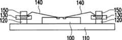
接着,请参考图2C,在本实施例的步骤(c)和步骤(d)中,将多个具有导电柱136的第一层的软板130配置于这些第一层的导电块120上,并将多条第一层的导线140以打线接合方式电性连接于第一层的芯片100与各个第一层的软板130之间。更进一步说,在第一层的软板130上制作导电柱136的步骤包括:在软性基材(例如聚酰亚胺)上以激光穿孔或光刻方式蚀刻所需的微通孔,接着,填入一导电材料于微通孔中,并覆盖一接垫材料(例如金)于导电材料上。请同时参考图2C、图3A以及图3B,而图3A及图3B分别绘示图2C之软板的俯视图以及沿着I-I线的剖面示意图。软性基材131的上表面的每一接垫132具有打线用的接垫部位132a以及用以配置导电块的接垫部位132b,其形状由上观之约为一匙形结构,而下方的每一接垫134则借由导电柱136与其上方的接垫132电性连接,并与其下方的导电块120电性连接,以达成相互堆叠的软板130之间的电性导通。Next, please refer to FIG. 2C. In step (c) and step (d) of this embodiment, a plurality of first-layer
值得注意的是,在软性基材上制作低深宽比的微通孔的成本相对于在硅基材上制作高深宽比的微通孔的成本低,且不会占用硅基材的可用面积,因此每一个晶圆可切割的最多芯片数不会因芯片尺寸变大而变少。此外,在软性基材上制作微通孔,不会对芯片内的集成电路的电性效能及可靠度有不良的影响,且软板具有较佳的重工性及可挠性,并可提高生产的效率及可靠度。It is worth noting that the cost of fabricating low-aspect-ratio microvias on soft substrates is lower than that of high-aspect-ratio microvias on silicon substrates, and does not occupy the available silicon substrate. Therefore, the maximum number of chips that can be cut per wafer will not decrease due to the increase in chip size. In addition, making micro-vias on a flexible substrate will not adversely affect the electrical performance and reliability of the integrated circuit in the chip, and the flexible board has better reworkability and flexibility, and can improve Production efficiency and reliability.
接着,请参考图2D,在本实施例的步骤(e)中,以打线结球的方式配置多个第二层的导电块150于第一层的软板130的导电柱136上,也就是配置在导电柱上方用以配置导电块150的接垫部位132b上。如此,第一层的导电块120与第二层的导电块150电性导通。Next, please refer to FIG. 2D. In step (e) of this embodiment, a plurality of
请参考图2E,在本实施例的步骤(f)和步骤(g)中,将第一层的间隙层160(例如环氧树脂)配置于第一层的芯片100上,并将第二层的芯片170配置于第一层的间隙层160上。也就是说,第一层的间隙层160配置于第一层的芯片100以及第二层的芯片170之间,用以保持相邻二芯片之间的间距,让第一层的导线140能有足够的打线高度而不至于崩塌。Please refer to FIG. 2E , in step (f) and step (g) of this embodiment, the gap layer 160 (such as epoxy resin) of the first layer is configured on the
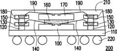
接着,请参考图2F,在本实施例的步骤(h)和步骤(i)中,将多个具有导电柱186的第二层的软板180配置于这些第二层的导电块150上,并将多条第二层的导线190以打线接合方式电性连接于第二层的芯片170与第二层的软板之间。更进一步说,各层的导电块120、150垂直排列于相互堆叠的软板130、180之间以及基板110上,以借由相互堆叠的导电块120、150及软板130、180的电性导通,让各层的芯片100、170与基板110电性连接,进而形成一具有二层芯片的堆叠结构200于基板110上。Next, please refer to FIG. 2F. In step (h) and step (i) of this embodiment, a plurality of second-layer
最后,请参考图2G和图2H,在本实施例中,以模穴覆盖于基板上,并填入液态的封胶于模穴内,接着固化液态的封胶使之成形,如此形成一封胶210于基板110上,且封胶210包覆此具有二层芯片的堆叠结构200,以隔绝外界的污染及湿气。接着,利用植球装置将多个焊球220配置于基板110的下表面,也就是配置在基板110的下表面的各个接垫上,接着回焊焊球使之成形,如此基板110可借由这些焊球220与外部电路板进行表面接合封装,以构成三维堆叠的多芯片模组。Finally, please refer to FIG. 2G and FIG. 2H. In this embodiment, the mold cavity is used to cover the substrate, and the liquid sealant is filled into the mold cavity, and then the liquid sealant is cured to shape it, thus forming a sealant. 210 is on the
以存储器模组而言,本发明除了形成具有二层芯片的堆叠结构之外,还可配置更多相互堆叠的存储器芯片,以增加存储容量。这些存储器芯片的数量可以依照存储容量的需求而增加,以构成具有N层芯片的堆叠结构于基板上,其中N为大于3的正整数。基板可以是印刷电路板或导线架等载体,基板可利用表面粘着技术将其接脚或焊球焊接于电路板上。此外,利用电路板上设置的插入式表面接合接口(例如金手指),存储器模组可插置于电脑的主机板的PCI插槽中,用以传输所需的资料。As far as the memory module is concerned, in addition to forming a stacked structure with two-layer chips, the present invention can also configure more memory chips stacked on each other to increase the storage capacity. The number of these memory chips can be increased according to the requirement of storage capacity to form a stacked structure with N layers of chips on the substrate, where N is a positive integer greater than 3. The substrate can be a carrier such as a printed circuit board or a lead frame, and the substrate can use surface mount technology to solder its pins or solder balls to the circuit board. In addition, the memory module can be inserted into the PCI slot of the motherboard of the computer by using the plug-in surface-bonding interface (such as golden finger) provided on the circuit board to transmit required data.
请参考图4及图5,其分别绘示本发明二实施例之堆叠式芯片封装结构的示意图。在图4中,芯片300的焊垫302排列于中央区域,因此打线制程所用的导线的行程较长,而在图5中,芯片300的焊垫302借由重布线层(图未示)转移到周围区域,因此打线制程所用的导线的行程较短。在此二堆叠式芯片封装结构中,多个芯片300配置于基板310的第一表面312(即上表面),而这些芯片300分别借由一间隙层304而相互堆叠,以符合打线高度。这些相互堆叠的芯片300由下而上依序以面对背(face to back)的方式堆叠。此外,多个第一导电块320垂直排列于相互堆叠的第一软板330之间,并与这些第一软板330的导电柱336电性连接;多个第二导电块350垂直排列于相互堆叠的第二软板360之间,并与这些第二软板360的导电柱366电性连接。另外,多条第一导线340电性连接于各层的第一软板330与芯片300之间,而多条第二导线370电性连接于各层的第二软板360与芯片300之间。如此,构成一具有四层芯片的封装结构于基板310上。另外,基板310的第一表面还可形成一封胶380,其包覆此具有四层芯片的封装结构,以隔绝外界的污染及湿气。基板310的第二表面314(即下表面)还可配置多个焊球390或其他导电结构,以进行表面接合封装。Please refer to FIG. 4 and FIG. 5 , which are respectively schematic diagrams of stacked chip packaging structures according to two embodiments of the present invention. In FIG. 4, the
在本实施例中,这些相互堆叠的软板区分为二部分,即是多个相互堆叠的第一软板330以及多个相互堆叠的第二软板360。第一软板330的数量与芯片300的数量一致,而第二软板360的数量与芯片300的数量一致。但在其他实施例中,相互堆叠的软板可依照实际需求区分为更多部分(或更少部分),以增加(或减少)资料输出/输入的数量。In this embodiment, the stacked flexible boards are divided into two parts, that is, a plurality of first
由上述的堆叠式芯片封装结构及其制程可知,本实施例由下而上依序配置第一层的芯片、导电块、第一软板、第二软板、导线以及间隙层,再配置第二层的芯片、导电块、第一软板、第二软板以及导线,若要进行更高层的封装制程,则重复步骤(f)至少一次,以配置第N-1层的间隙层于第N-1层的芯片上;重复步骤(g)至少一次,以配置第N层的芯片于该第N-1层的间隙层上;重复步骤(e)至少一次,以打线结球的方式配置多个第N层的导电块于第N-1层的软板上;重复步骤(h)至少一次,以配置第N层的软板于这些第N层的导电块上;重复步骤(i)至少一次,以将多条第N层的导线以打线接合方式电性连接于第N层的芯片与第N层的软板之间。如此,形成一具有N层芯片的堆叠结构于基板上。From the above-mentioned stacked chip packaging structure and its manufacturing process, it can be seen that in this embodiment, the chip on the first layer, the conductive block, the first flexible board, the second flexible board, the wires and the gap layer are arranged sequentially from bottom to top, and then the second layer is arranged. For the second-layer chip, conductive block, first flexible board, second flexible board, and wires, if a higher-level packaging process is to be performed, step (f) is repeated at least once to configure the gap layer of the N-1th layer on the second layer. On the chip of the N-1 layer; repeat step (g) at least once, to configure the chip of the Nth layer on the gap layer of the N-1 layer; repeat step (e) at least once, in the mode of knotting and balling Configure a plurality of conductive blocks of the Nth layer on the flexible board of the N-1 layer; repeat step (h) at least once, to configure the flexible board of the Nth layer on the conductive blocks of the Nth layer; repeat step (i ) at least once, so as to electrically connect a plurality of wires of the Nth layer between the chip of the Nth layer and the flexible board of the Nth layer by wire bonding. In this way, a stacked structure with N-layer chips is formed on the substrate.
综上所述,本发明将具有导电柱的软板依序堆叠于导电块上,并使各层的芯片与软板之间借由各层的导线电性连接,以形成具有多层芯片的封装结构于一基板上。利用本发明的堆叠式芯片封装结构及其制作方法,可有效地增加存储容量、降低成本,并使高密度封装的存储器模组具有优良的电性效能及可靠度。此外,由于在软板上制作导电柱,不会对芯片内的集成电路的电性效能及可靠度有不良的影响,且软板具有较佳的重工性及可挠性,并可提高生产的效率。To sum up, the present invention stacks the flexible boards with conductive pillars on the conductive block in sequence, and electrically connects the chips and the flexible boards of each layer through the wires of each layer to form a multi-layer chip. The packaging structure is on a substrate. Utilizing the stacked chip packaging structure and the manufacturing method thereof of the present invention can effectively increase storage capacity, reduce cost, and enable high-density packaged memory modules to have excellent electrical performance and reliability. In addition, since the conductive pillars are made on the flexible board, there will be no adverse effect on the electrical performance and reliability of the integrated circuit in the chip, and the flexible board has better reworkability and flexibility, and can improve production efficiency. efficiency.
虽然本发明已以较佳实施例揭示如上,然其并非用以限定本发明,任何本领域技术人员,在不脱离本发明的精神和范围内,当可作些许的修改和完善,因此本发明的保护范围当以权利要求书所界定的为准。Although the present invention has been disclosed above with preferred embodiments, it is not intended to limit the present invention. Any person skilled in the art may make some modifications and improvements without departing from the spirit and scope of the present invention. Therefore, the present invention The scope of protection should be defined by the claims.
Claims (12)
Priority Applications (1)
| Application Number | Priority Date | Filing Date | Title |
|---|---|---|---|
| CN2007101601848ACN101465341B (en) | 2007-12-21 | 2007-12-21 | Stacked Chip Package Structure |
Applications Claiming Priority (1)
| Application Number | Priority Date | Filing Date | Title |
|---|---|---|---|
| CN2007101601848ACN101465341B (en) | 2007-12-21 | 2007-12-21 | Stacked Chip Package Structure |
Publications (2)
| Publication Number | Publication Date |
|---|---|
| CN101465341Atrue CN101465341A (en) | 2009-06-24 |
| CN101465341B CN101465341B (en) | 2011-07-06 |
Family
ID=40805819
Family Applications (1)
| Application Number | Title | Priority Date | Filing Date |
|---|---|---|---|
| CN2007101601848AActiveCN101465341B (en) | 2007-12-21 | 2007-12-21 | Stacked Chip Package Structure |
Country Status (1)
| Country | Link |
|---|---|
| CN (1) | CN101465341B (en) |
Cited By (3)
| Publication number | Priority date | Publication date | Assignee | Title |
|---|---|---|---|---|
| WO2015184948A1 (en)* | 2014-06-05 | 2015-12-10 | 华为技术有限公司 | Chip stacking package structure and electronic device |
| CN107195613A (en)* | 2017-06-23 | 2017-09-22 | 华进半导体封装先导技术研发中心有限公司 | Three-dimension packaging structure and its manufacture method based on different height copper post |
| CN107195617A (en)* | 2017-06-23 | 2017-09-22 | 华进半导体封装先导技术研发中心有限公司 | Three-dimension packaging structure and its manufacture method based on different height copper post |
Family Cites Families (3)
| Publication number | Priority date | Publication date | Assignee | Title |
|---|---|---|---|---|
| KR0134648B1 (en)* | 1994-06-09 | 1998-04-20 | 김광호 | Low Noise Multilayer Chip Package |
| CN1214460C (en)* | 2000-11-27 | 2005-08-10 | 矽品精密工业股份有限公司 | Enhanced Thermal Quad Flat No Lead Package |
| CN2726111Y (en)* | 2004-06-22 | 2005-09-14 | 胜开科技股份有限公司 | Stacked integrated circuit package assembly |
- 2007
- 2007-12-21CNCN2007101601848Apatent/CN101465341B/enactiveActive
Cited By (3)
| Publication number | Priority date | Publication date | Assignee | Title |
|---|---|---|---|---|
| WO2015184948A1 (en)* | 2014-06-05 | 2015-12-10 | 华为技术有限公司 | Chip stacking package structure and electronic device |
| CN107195613A (en)* | 2017-06-23 | 2017-09-22 | 华进半导体封装先导技术研发中心有限公司 | Three-dimension packaging structure and its manufacture method based on different height copper post |
| CN107195617A (en)* | 2017-06-23 | 2017-09-22 | 华进半导体封装先导技术研发中心有限公司 | Three-dimension packaging structure and its manufacture method based on different height copper post |
Also Published As
| Publication number | Publication date |
|---|---|
| CN101465341B (en) | 2011-07-06 |
Similar Documents
| Publication | Publication Date | Title |
|---|---|---|
| JP5002533B2 (en) | Stacked chip package structure | |
| JP4068974B2 (en) | Semiconductor device | |
| US8729690B2 (en) | Assembly having stacked die mounted on substrate | |
| US7704794B2 (en) | Method of forming a semiconductor device | |
| CN104064551B (en) | A kind of chip stack package structure and electronic equipment | |
| US20150200183A1 (en) | Stackable microelectronic package structures | |
| US8786069B1 (en) | Reconfigurable pop | |
| CN113169157B (en) | Double-sided mountable large MCM package with reduced memory channel length | |
| CN107978532A (en) | Method for forming stacked package structure | |
| US20120146216A1 (en) | Semiconductor package and fabrication method thereof | |
| CN101359659A (en) | Semiconductor package and manufacturing method, semiconductor module and device including the module | |
| KR20110099555A (en) | Stacked Semiconductor Packages | |
| JP5394603B2 (en) | A multi-package module comprising a stacked package comprising a die and a mold body arranged asymmetrically. | |
| KR20130000319A (en) | Integrated circuit packaging system with vertical interconnects and method of manufacture thereof | |
| CN101192544B (en) | Stack structure of semiconductor element embedded in bearing plate and manufacturing method thereof | |
| CN101477979A (en) | Multi-chip encapsulation body | |
| US20080258288A1 (en) | Semiconductor device stack package, electronic apparatus including the same, and method of manufacturing the same | |
| CN101465341B (en) | Stacked Chip Package Structure | |
| CN102769009A (en) | semiconductor package | |
| TWI710078B (en) | Conductive wire through-mold connection apparatus and method | |
| CN115700920A (en) | Semiconductor package including stacked chip structure | |
| KR101185858B1 (en) | Semiconductor chip and stacked semiconductor package having the same | |
| CN100552940C (en) | Stack structure of semiconductor element embedded loading board | |
| CN221783207U (en) | Chip packaging structure and electronic equipment | |
| US9659848B1 (en) | Stiffened wires for offset BVA |
Legal Events
| Date | Code | Title | Description |
|---|---|---|---|
| C06 | Publication | ||
| PB01 | Publication | ||
| C10 | Entry into substantive examination | ||
| SE01 | Entry into force of request for substantive examination | ||
| C14 | Grant of patent or utility model | ||
| GR01 | Patent grant |