CN101464742A - Touch control device and method thereof - Google Patents
Touch control device and method thereofDownload PDFInfo
- Publication number
- CN101464742A CN101464742ACNA2007101997008ACN200710199700ACN101464742ACN 101464742 ACN101464742 ACN 101464742ACN A2007101997008 ACNA2007101997008 ACN A2007101997008ACN 200710199700 ACN200710199700 ACN 200710199700ACN 101464742 ACN101464742 ACN 101464742A
- Authority
- CN
- China
- Prior art keywords
- conductive layer
- conductive
- substrate
- scanning
- sensing circuit
- Prior art date
- Legal status (The legal status is an assumption and is not a legal conclusion. Google has not performed a legal analysis and makes no representation as to the accuracy of the status listed.)
- Granted
Links
Images


Classifications
- G—PHYSICS
- G06—COMPUTING OR CALCULATING; COUNTING
- G06F—ELECTRIC DIGITAL DATA PROCESSING
- G06F3/00—Input arrangements for transferring data to be processed into a form capable of being handled by the computer; Output arrangements for transferring data from processing unit to output unit, e.g. interface arrangements
- G06F3/01—Input arrangements or combined input and output arrangements for interaction between user and computer
- G06F3/03—Arrangements for converting the position or the displacement of a member into a coded form
- G06F3/041—Digitisers, e.g. for touch screens or touch pads, characterised by the transducing means
- G06F3/0416—Control or interface arrangements specially adapted for digitisers
- G06F3/04166—Details of scanning methods, e.g. sampling time, grouping of sub areas or time sharing with display driving
- G—PHYSICS
- G06—COMPUTING OR CALCULATING; COUNTING
- G06F—ELECTRIC DIGITAL DATA PROCESSING
- G06F3/00—Input arrangements for transferring data to be processed into a form capable of being handled by the computer; Output arrangements for transferring data from processing unit to output unit, e.g. interface arrangements
- G06F3/01—Input arrangements or combined input and output arrangements for interaction between user and computer
- G06F3/03—Arrangements for converting the position or the displacement of a member into a coded form
- G06F3/041—Digitisers, e.g. for touch screens or touch pads, characterised by the transducing means
- G06F3/044—Digitisers, e.g. for touch screens or touch pads, characterised by the transducing means by capacitive means
- G06F3/0445—Digitisers, e.g. for touch screens or touch pads, characterised by the transducing means by capacitive means using two or more layers of sensing electrodes, e.g. using two layers of electrodes separated by a dielectric layer
- G—PHYSICS
- G06—COMPUTING OR CALCULATING; COUNTING
- G06F—ELECTRIC DIGITAL DATA PROCESSING
- G06F3/00—Input arrangements for transferring data to be processed into a form capable of being handled by the computer; Output arrangements for transferring data from processing unit to output unit, e.g. interface arrangements
- G06F3/01—Input arrangements or combined input and output arrangements for interaction between user and computer
- G06F3/03—Arrangements for converting the position or the displacement of a member into a coded form
- G06F3/041—Digitisers, e.g. for touch screens or touch pads, characterised by the transducing means
- G06F3/044—Digitisers, e.g. for touch screens or touch pads, characterised by the transducing means by capacitive means
- G06F3/0446—Digitisers, e.g. for touch screens or touch pads, characterised by the transducing means by capacitive means using a grid-like structure of electrodes in at least two directions, e.g. using row and column electrodes
Landscapes
- Engineering & Computer Science (AREA)
- General Engineering & Computer Science (AREA)
- Theoretical Computer Science (AREA)
- Human Computer Interaction (AREA)
- Physics & Mathematics (AREA)
- General Physics & Mathematics (AREA)
- Position Input By Displaying (AREA)
Abstract
Description
Translated fromChinese技术领域technical field
本发明是关于一种触控装置,特别是关于一种循序扫描的触控装置及其方法。The present invention relates to a touch device, in particular to a sequential scanning touch device and its method.
背景技术Background technique
传统触摸板结构主要包括有一玻璃基板(Glass Substrate),在其表面涂布有一层透明导电层(例如氧化铟锡ITO导电层),玻璃基板与透明导电层组成一导电玻璃。导电玻璃上设有另一玻璃基板或薄膜,并在该玻璃基板或薄膜的底面涂布有一透明导电层,其相对应于玻璃基板的透明导电层。在玻璃基板的透明导电层与薄膜的透明导电层之间具有复数个绝缘隔点,用以隔开该透明导电层与透明导电层。The traditional touch panel structure mainly includes a glass substrate (Glass Substrate), coated with a layer of transparent conductive layer (such as indium tin oxide ITO conductive layer) on its surface, the glass substrate and transparent conductive layer form a conductive glass. Another glass substrate or film is arranged on the conductive glass, and a transparent conductive layer is coated on the bottom surface of the glass substrate or film, which corresponds to the transparent conductive layer of the glass substrate. Between the transparent conductive layer of the glass substrate and the transparent conductive layer of the film, there are a plurality of insulating spacers for separating the transparent conductive layer from the transparent conductive layer.
发明内容Contents of the invention
在不同的触摸板结构设计中,配合不同的扫描方法及计算公式,虽然都可以判别出触摸板的受触压位置。但各种不同的技术都有其缺失。在有些触摸板的触压位置检测方法中,有些需搭配复杂的电路设计,有些则必须搭配繁杂的计算公式。In different structural designs of the touchpad, with different scanning methods and calculation formulas, although the touched position of the touchpad can be judged. But each of the different technologies has its drawbacks. In some touch position detection methods of touch panels, some need to be matched with complicated circuit design, and some need to be matched with complex calculation formulas.
缘此,本发明的主要目的即是提供一种触控装置,在进行触压位置的检测时,仅对两个导电层的其中一个导电层的其中一端或两端进行循序扫描,而另一个导电层形成一均一电位值或梯度电位值,即可由微控器计算出用户触压位置。For this reason, the main purpose of the present invention is to provide a touch device, which only sequentially scans one or both ends of one of the two conductive layers when detecting the position of the touch pressure, while the other The conductive layer forms a uniform potential value or a gradient potential value, and the microcontroller can calculate the user's touch position.
本发明的另一目的是提供一种循序扫描触摸板导电层的导电长条的一端或两端以检测触压位置的方法,在对导电长条的一端或两端进行循序扫描时,微控器依据导电长条的电压状况可检测在该导电长条不同位置受触压的位置。Another object of the present invention is to provide a method for sequentially scanning one or both ends of the conductive strip of the touch panel conductive layer to detect the touch position. When sequentially scanning one or both ends of the conductive strip, the micro-controller According to the voltage status of the conductive long strip, the device can detect the positions that are pressed at different positions of the conductive long strip.
本发明解决问题的技术手段:The technical means of the present invention to solve the problem:
本发明为解决现有技术的问题所采用的技术手段是在一触摸板的第一导电层施加一均一电位或梯度电位的驱动电压,而在第二导电层的其中一端或两端经由扫描线连接至一扫描感测电路。在检测触压位置时,是以扫描感测电路对该第二导电层的各个导电长条的第一端或两端重复循序扫描。依据该扫描感测电路对该第二导电层的各个导电长条的扫描及由该第一导电层受触压而施加至该受触压位置所对应的第二导电层的导电长条的电压而计算出该被触压位置的坐标位置。The technical means adopted by the present invention to solve the problems of the prior art is to apply a driving voltage of a uniform potential or a gradient potential to the first conductive layer of a touch panel, and at one or both ends of the second conductive layer to Connect to a scan sense circuit. When detecting the touch position, the first end or both ends of each conductive strip of the second conductive layer are repeatedly scanned sequentially by the scanning sensing circuit. According to the scanning of each conductive strip of the second conductive layer by the scanning sensing circuit and the voltage applied from the first conductive layer to the conductive strip of the second conductive layer corresponding to the touched position And calculate the coordinate position of the touched position.
本发明对照先前技术的功效:The present invention contrasts the effect of prior art:
由于本发明在进行触压位置的检测时,对触摸板的一导电层的各个导电长条的一端或两端进行扫描检测,故在扫描控制方法及搭配的扫描电路方面皆极为简易,且微控器在计算用户触压位置时,也仅需简易的电压计算公式即可检测在该导电长条不同位置受触压的位置。相较于现有技术,本发明所采用的技术具有触压位置计算简易、快速、电路简化的优点。Since the present invention scans and detects one end or both ends of each conductive strip of a conductive layer of the touch panel when detecting the touch position, it is very simple in terms of scanning control method and matching scanning circuit, and micro When the controller calculates the position of the user's touch pressure, it only needs a simple voltage calculation formula to detect the position of the touch pressure at different positions of the conductive strip. Compared with the prior art, the technology adopted in the present invention has the advantages of simple and fast calculation of the touch pressure position and simplified circuit.
附图说明Description of drawings
图1显示本发明第一实施例触控装置的系统方块图;FIG. 1 shows a system block diagram of a touch device according to a first embodiment of the present invention;
图2显示图1中第一基板及第二基板在对应组合后的立体分解图;Fig. 2 shows the three-dimensional exploded view of the first substrate and the second substrate in Fig. 1 after corresponding combination;
图3显示图1中扫描感测电路对各个导电长条的第一端循序扫描时的时序表;FIG. 3 shows a timing table when the scanning sensing circuit sequentially scans the first ends of each conductive strip in FIG. 1;
图4显示本发明第二实施例的系统方块图;Fig. 4 shows the system block diagram of the second embodiment of the present invention;
图5显示图4中扫描感测电路对各个导电长条的第一端及第二端循序扫描时的时序表;FIG. 5 shows a timing table when the scanning sensing circuit in FIG. 4 sequentially scans the first end and the second end of each conductive strip;
图6显示本发明第三实施例的系统方块图;Fig. 6 shows the system block diagram of the third embodiment of the present invention;
图7显示图6中第一导电层形成有一电压梯度型态的梯度电位值的示意图;FIG. 7 shows a schematic diagram of the gradient potential value of the first conductive layer formed with a voltage gradient type in FIG. 6;
图8显示本发明第四实施例的系统方块图;Fig. 8 shows the system block diagram of the fourth embodiment of the present invention;
图9为显示本发明第五实施例的系统方块图;9 is a system block diagram showing a fifth embodiment of the present invention;
图10显示图9中第一基板及第二基板对应组合的立体分解图;FIG. 10 shows a three-dimensional exploded view of the corresponding combination of the first substrate and the second substrate in FIG. 9;
图11显示本发明第六实施例的系统方块图;Fig. 11 shows the system block diagram of the sixth embodiment of the present invention;
图12显示本发明第七实施例的系统方块图;Fig. 12 shows the system block diagram of the seventh embodiment of the present invention;
图13显示图12中第一导电层的导电长条形成有一电压梯度型态的梯度电位值的示意图;FIG. 13 shows a schematic diagram of the gradient potential value of a voltage gradient type formed by the conductive strips of the first conductive layer in FIG. 12;
图14显示本发明第八实施例的系统方块图。FIG. 14 shows a system block diagram of an eighth embodiment of the present invention.
附图标号:Figure number:
100、100a、100b、100c、100d、 触摸板100, 100a, 100b, 100c, 100d, Touchpad
100e、100f、100g100e, 100f, 100g
1 第一基板1 The first substrate
10 连续平面结构的第一导电层10 The first conductive layer of the continuous planar structure
11 导电长条结构的第一导电层11 The first conductive layer of the conductive strip structure
2 第二基板2 Second Substrate
21 第二导电层21 Second conductive layer
3 绝缘隔点3 Insulation point
4 驱动电压供应电路4 Driving voltage supply circuit
5 微控器5 Microcontroller
6 扫描感测电路6 Scan sensing circuit
61、61a 扫描线61, 61a Scanning line
7 模拟至数字转换电路7 Analog to digital conversion circuit
S1 驱动电压控制信号S1 Driving voltage control signal
S2 扫描控制信号S2 Scan control signal
S3 扫描感测信号S3 Scan sensing signal
X1、X2、X3...Xn 导电长条X1, X2, X3...Xn Conductive strip
X1a 第一端X1a First end
X1b 第二端X1b Second end
Y1、Y2、Y3...Yn 导电长条Y1, Y2, Y3...Yn Conductive strip
Y1a、Y2a、Y3a、Yna 第一端Y1a, Y2a, Y3a, Yna First end
Y1b、Y2b、Y3b、Ynb 第二端Y1b, Y2b, Y3b, Ynb Second terminal
V 驱动电压V Driving Voltage
G 接地线G Ground wire
Y 第一方向Y First Direction
X 第二方向X Second direction
具体实施方式Detailed ways
本发明所采用的具体实施例,将通过以下的实施例及附图作进一步的说明。The specific embodiments adopted by the present invention will be further described through the following embodiments and accompanying drawings.
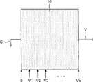
参阅图1所示,其显示本发明第一实施例的系统方块图。如图所示,一触摸板100包括有一第一基板1及一相对应的第二基板2,在该第一基板1的底面形成有一连续平面结构的第一导电层10,而在该第二基板2的顶面形成有一第二导电层21。以目前的触摸板结构而言,一般是在玻璃基板表面涂布一层透明导电层(例如氧化铟锡ITO导电层)作为该连续平面结构的第一导电层10与第二导电层21。Referring to FIG. 1 , it shows a system block diagram of the first embodiment of the present invention. As shown in the figure, a
图2显示第一基板1及第二基板2在对应组合后,连续平面结构的第一导电层10相对应于第二导电层21,且两者之间以复数个绝缘隔点3予以隔开。Figure 2 shows that after the
连续平面结构的第一导电层10是在第一基板1的表面均匀涂布一层透明导电层,且在该连续平面结构的第一导电层10施加一预定电压准位的驱动电压V,如此即在该连续平面结构的第一导电层10建立一均一的电位值。The first
第二导电层21包含复数个导电长条Y1、Y2、Y3...Yn,各导电长条Y1、Y2、Y3...Yn彼此平行且不相接触。每一个导电长条Y1、Y2、Y3...Yn以一第一方向Y延伸于第二基板2的顶面。The second
第二导电层21的各个导电长条Y1、Y2、Y3...Yn的第一端Y1a、Y2a、Y3a...Yna是通过数条扫描线61分别连接至一扫描感测电路6(例如可采用现有的多任务器),而各个导电长条Y1、Y2、Y3...Yn的第二端Y1b、Y2b、Y3b...Ynb呈开放端。微控器5经由一扫描控制信号S2可控制扫描感测电路6对各个导电长条Y1、Y2、Y3...Yn的第一端Y1a、Y2a、Y3a...Yna循序扫描,以感测出各个导电长条Y1、Y2、Y3...Yn是否与连续平面结构的第一导电层10有被触压接触的状况及受触压点的位置。The first ends Y1a, Y2a, Y3a...Yna of the respective conductive strips Y1, Y2, Y3...Yn of the second
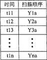
图3显示扫描感测电路6对各个导电长条Y1、Y2、Y3...Yn的第一端Y1a、Y2a、Y3a...Yna循序扫描时的时序表。当第一时间t1时,扫描感测电路6首先对导电长条Y1的第一端Y1a扫描。接着在第二时间t2时,对导电长条Y2的第一端Y2a扫描。第三时间t3时,对导电长条Y3的第一端Y3a扫描。最后在第n时间tn时,对导电长条Yn的第一端Yna扫描。完成前述一周期的扫描之后,重复前述步骤持续对各个导电长条Y1、Y2、Y3...Yn的单端循序扫描。FIG. 3 shows a timing table when the
经由扫描感测电路6扫描第二导电层21的各个导电长条Y1、Y2、Y3...Yn时,会将得到的扫描感测信号S3经由一模拟至数字转换电路7转换为数字型态的扫描感测信号,再送至微控器5中。When scanning the respective conductive strips Y1, Y2, Y3 . The scanning sensing signal is sent to the
当第一基板1的表面受到触压操作时,连续平面结构的第一导电层10会与第二导电层21在被触压位置点接触,故由该连续平面结构的第一导电层10依据该受触压位置而施加驱动电压V至该受触压位置所对应的第二导电层21的导电长条Y1、Y2、Y3...或Yn,该微控器5再依据该扫描感测电路6对该第二导电层21的各个导电长条Y1、Y2、Y3...或Yn扫描感测所产生的扫描感测信号S3,而由微控器5计算出该触摸板的被触压位置的X、Y轴坐标。When the surface of the
例如当用户触压到连续平面结构的第一导电层10与第二导电层21的第三个导电长条Y3时,连续平面结构的第一导电层10的驱动电压V即会施加至该第二导电层21的第三个导电长条Y3。For example, when the user touches the third conductive strip Y3 of the first
当扫描感测电路6扫描到该第二导电层21的第三个导电长条Y3时,即可决定出用户触压的位置是在第三个导电长条Y3上,然后微控器5再依据该驱动电压V在该第三个导电长条Y3的第一端Y3a的电压状况,而进一步计算出用户触压位置的X、Y轴坐标位置。When the
图4为显示本发明第二实施例的系统方块图。此一实施例与前述第一实施例大致相同,其差异在于此一实施例触摸板100a的第二导电层21的各个导电长条Y1、Y2、Y3...Yn的第一端Y1a、Y2a、Y3a...Yna除了经由扫描线61连接至扫描感测电路6之外,各个导电长条Y1、Y2、Y3...Yn的第二端Y1b、Y2b、Y3b...Ynb另经由扫描线61a连接至扫描感测电路6,故扫描感测电路6可经由扫描线61、61a分别对各个导电长条Y1、Y2、Y3...Yn的第一端Y1a、Y2a、Y3a...Yna及第二端Y1b、Y2b、Y3b...Ynb循序扫描,以感测出各个导电长条Y1、Y2、Y3...Yn是否与连续平面结构的第一导电层10有被触压接触的状况及受触压点的位置。FIG. 4 is a system block diagram showing a second embodiment of the present invention. This embodiment is substantially the same as the aforementioned first embodiment, the difference lies in the first ends Y1a, Y2a of the respective conductive strips Y1, Y2, Y3...Yn of the second
图5显示扫描感测电路6对各个导电长条Y1、Y2、Y3...Yn的第一端Y1a、Y2a、Y3a...Yna及第二端Y1b、Y2b、Y3b...Ynb循序扫描时的时序表。扫描感测电路6会在不同时间t11、t12、t13...t1n时,对导电长条Y1、Y2、Y3...Yn的第一端Y1a、Y2a、Y3a...Yna循序扫描,接着在不同时间t21、t22、t23...t1n时,对导电长条Y1、Y2、Y3...Yn的第二端Y1b、Y2b、Y3b...Ynb循序扫描。完成前述一周期的扫描之后,重复前述步骤持续对各个导电长条Y1、Y2、Y3...Yn的双端循序扫描。FIG. 5 shows that the
图6为显示本发明第三实施例的系统方块图。此一实施例与前述第一实施例大致相同,其差异在于此一实施例触摸板100b的连续平面结构的第一导电层10的一端施加一预定电压准位的驱动电压V,而另一端则经由一接地线G接地,如此可在该连续平面结构的第一导电层10上建立一梯度电位值。FIG. 6 is a system block diagram showing a third embodiment of the present invention. This embodiment is substantially the same as the aforementioned first embodiment, the difference being that one end of the first
图7显示图6中第一导电层形成有一电压梯度型态的梯度电位值的示意图。FIG. 7 shows a schematic diagram of gradient potential values in a voltage gradient type formed on the first conductive layer in FIG. 6 .
图8为显示本发明第四实施例的系统方块图。此一实施例与图4所示第二实施例大致相同,其差异在于此一实施例触摸板100c的连续平面结构的第一导电层10的一端施加一预定电压准位的驱动电压V,而另一端则经由一接地线G接地,如此可在该连续平面结构的第一导电层10上建立一梯度电位值。FIG. 8 is a system block diagram showing a fourth embodiment of the present invention. This embodiment is substantially the same as the second embodiment shown in FIG. 4, the difference being that one end of the first
图9为显示本发明第五实施例的系统方块图。此一实施例与图1所示第一实施例大致相同,其差异在于此一实施例触摸板100d的连续平面结构的第一导电层10改为导电长条结构的第一导电层11,其包含复数个导电长条X1、X2、X3...Xn构成一等效的连续平面结构。各导电长条X1、X2、X3...Xn彼此平行且不相接触。每一个导电长条X1、X2、X3...Xn以一第二方向X延伸于第一基板1的底面,并在各个导电长条X1、X2、X3...Xn的两端形成第一端及第二端,例如导电长条X1的两端分别形成为第一端X1a及第二端X1b。FIG. 9 is a system block diagram showing a fifth embodiment of the present invention. This embodiment is substantially the same as the first embodiment shown in FIG. 1, the difference being that the first
图10显示图9中第一基板1及第二基板2在对应组合后,导电长条结构的第一导电层11相对应于第二导电层21,且两者之间以复数个绝缘隔点3予以隔开。Figure 10 shows that after the corresponding combination of the
各个导电长条X1、X2、X3...Xn的第一端X1a是经由一连接线连接至一驱动电压供应电路4取得一预定电压准位的驱动电压V,而在各个导电长条X1、X2、X3...Xn的第二端X1b呈开放端。如此在各个导电长条X1、X2、X3...Xn建立一均一的电位值。The first end X1a of each conductive strip X1, X2, X3...Xn is connected to a driving
图11为显示本发明第六实施例的系统方块图。此一实施例与图9所示实施例大致相同,其差异在于此一实施例触摸板100e的第二导电层21的各个导电长条Y1、Y2、Y3...Yn的第一端Y1a、Y2a、Y3a...Yna除了经由扫描线61连接至扫描感测电路6之外,各个导电长条Y1、Y2、Y3...Yn的第二端Y1b、Y2b、Y3b...Ynb另经由扫描线61a连接至扫描感测电路6,故扫描感测电路6可经由扫描线61、61a分别对各个导电长条Y1、Y2、Y3...Yn的第一端Y1a、Y2a、Y3a...Yna及第二端Y1b、Y2b、Y3b...Ynb循序扫描,以感测出各个导电长条Y1、Y2、Y3...Yn是否与导电长条结构的第一导电层11有被触压接触的状况及受触压点的位置。FIG. 11 is a system block diagram showing a sixth embodiment of the present invention. This embodiment is substantially the same as the embodiment shown in FIG. 9 , the difference being that the first ends Y1a, Y1, Y2, Y3... In addition to connecting Y2a, Y3a...Yna to the
图12为显示本发明第七实施例的系统方块图。此一实施例与图9所示实施例大致相同,其差异在于此一实施例触摸板100f中,各导电长条X1、X2、X3...Xn的第一端X1a施加一预定电压准位的驱动电压V,而第二端X1b则经由一接地线G接地,如此可在各导电长条X1、X2、X3...Xn上建立一梯度电位值。FIG. 12 is a system block diagram showing a seventh embodiment of the present invention. This embodiment is substantially the same as the embodiment shown in FIG. 9, the difference is that in the
图13显示图12中第一导电层的导电长条形成有一电压梯度型态的梯度电位值的示意图。FIG. 13 shows a schematic diagram of gradient potential values in a voltage gradient pattern formed by the conductive strips of the first conductive layer in FIG. 12 .
图14为显示本发明第八实施例的系统方块图。此一实施例与图12所示实施例大致相同,其差异在于此一实施例触摸板100g中,第二导电层21的各个导电长条Y1、Y2、Y3...Yn的第一端Y1a、Y2a、Y3a...Yna除了经由扫描线61连接至扫描感测电路6之外,各个导电长条Y1、Y2、Y3...Yn的第二端Y1b、Y2b、Y3b...Ynb另经由扫描线61a连接至扫描感测电路6,故扫描感测电路6可经由扫描线61、61a分别对各个导电长条Y1、Y2、Y3...Yn的第一端Y1a、Y2a、Y3a...Yna及第二端Y1b、Y2b、Y3b...Ynb循序扫描,以感测出各个导电长条Y1、Y2、Y3...Yn是否与导电长条结构的第一导电层11有被触压接触的状况及受触压点的位置。FIG. 14 is a system block diagram showing an eighth embodiment of the present invention. This embodiment is substantially the same as the embodiment shown in FIG. 12 , the difference is that in the touch panel 100g of this embodiment, the first ends Y1a of the respective conductive strips Y1, Y2, Y3...Yn of the second
由以上的实施例可知,本发明确具产业上的利用价值,故本发明业已符合于专利的要件。惟以上的叙述仅为本发明的较佳实施例说明,凡精于此项技艺者当可依据上述的说明而作其它种种的改良,惟这些改变仍属于本发明的发明精神及权利要求范围中。From the above examples, it can be seen that the present invention clearly has industrial application value, so the present invention already meets the requirements of a patent. But the above description is only a description of the preferred embodiment of the present invention, and those skilled in this art can make other various improvements based on the above description, but these changes still belong to the spirit of the present invention and the scope of the claims .
Claims (12)
Translated fromChinesePriority Applications (1)
| Application Number | Priority Date | Filing Date | Title |
|---|---|---|---|
| CN2007101997008ACN101464742B (en) | 2007-12-17 | 2007-12-17 | Touch control device and method thereof |
Applications Claiming Priority (1)
| Application Number | Priority Date | Filing Date | Title |
|---|---|---|---|
| CN2007101997008ACN101464742B (en) | 2007-12-17 | 2007-12-17 | Touch control device and method thereof |
Publications (2)
| Publication Number | Publication Date |
|---|---|
| CN101464742Atrue CN101464742A (en) | 2009-06-24 |
| CN101464742B CN101464742B (en) | 2010-11-10 |
Family
ID=40805357
Family Applications (1)
| Application Number | Title | Priority Date | Filing Date |
|---|---|---|---|
| CN2007101997008AExpired - Fee RelatedCN101464742B (en) | 2007-12-17 | 2007-12-17 | Touch control device and method thereof |
Country Status (1)
| Country | Link |
|---|---|
| CN (1) | CN101464742B (en) |
Cited By (3)
| Publication number | Priority date | Publication date | Assignee | Title |
|---|---|---|---|---|
| CN102576260A (en)* | 2009-09-11 | 2012-07-11 | 辛纳普蒂克斯公司 | Input device based on voltage gradient |
| CN103186270A (en)* | 2011-12-27 | 2013-07-03 | 宸鸿光电科技股份有限公司 | Sensing electrode structure and touch panel using same |
| CN103186301A (en)* | 2011-12-30 | 2013-07-03 | 宸鸿光电科技股份有限公司 | Touch sensing device and programmable controller thereof |
Family Cites Families (4)
| Publication number | Priority date | Publication date | Assignee | Title |
|---|---|---|---|---|
| US4587378A (en)* | 1984-07-30 | 1986-05-06 | Koala Technologies Corporation | Two-layer touch tablet |
| EP0435438B1 (en)* | 1989-12-28 | 1998-03-04 | Gunze Limited | Input system including resistance film touch panel |
| CN1251170C (en)* | 2002-07-23 | 2006-04-12 | 李友端 | Touch type liquid crystal display and touch method thereof |
| CN1313911C (en)* | 2003-04-24 | 2007-05-02 | 海德威电子工业股份有限公司 | Coordinate detection method and system for touch panel |
- 2007
- 2007-12-17CNCN2007101997008Apatent/CN101464742B/ennot_activeExpired - Fee Related
Cited By (5)
| Publication number | Priority date | Publication date | Assignee | Title |
|---|---|---|---|---|
| CN102576260A (en)* | 2009-09-11 | 2012-07-11 | 辛纳普蒂克斯公司 | Input device based on voltage gradient |
| CN102576260B (en)* | 2009-09-11 | 2015-11-25 | 辛纳普蒂克斯公司 | Input device based on voltage gradient |
| CN103186270A (en)* | 2011-12-27 | 2013-07-03 | 宸鸿光电科技股份有限公司 | Sensing electrode structure and touch panel using same |
| CN103186270B (en)* | 2011-12-27 | 2016-08-10 | 宸鸿光电科技股份有限公司 | Sensing electrode structure and touch panel using the sensing electrode structure |
| CN103186301A (en)* | 2011-12-30 | 2013-07-03 | 宸鸿光电科技股份有限公司 | Touch sensing device and programmable controller thereof |
Also Published As
| Publication number | Publication date |
|---|---|
| CN101464742B (en) | 2010-11-10 |
Similar Documents
| Publication | Publication Date | Title |
|---|---|---|
| KR100993907B1 (en) | Touch control device and method | |
| CN101833387B (en) | Pressure sensitive touch device | |
| TWI387915B (en) | Method for detecting touch points of touch device | |
| TWI398800B (en) | Touch panel and output method therefor | |
| KR100952017B1 (en) | Apparatus and method for scanning and detecting touch points of touch control panel | |
| WO2010099678A1 (en) | Integrated touch control device | |
| TW201013485A (en) | Touch-control position sensing method for a touch-control device | |
| CN104252279A (en) | Touch display panel, manufacturing method of touch display panel, drive method of touch display panel and touch display device with touch display panel | |
| CN105786287B (en) | Touch display device and driving method thereof | |
| TWI765056B (en) | Position sensing device and position sensing method | |
| CN110045861A (en) | Capacitive detection circuit and electrostatic capacitance sensor equipment | |
| CN101464742A (en) | Touch control device and method thereof | |
| CN204066082U (en) | Touch-control display panel and touch control display apparatus | |
| CN101539825B (en) | Device and method for judging multi-touch positions of projected capacitive touch panel | |
| CN101464768A (en) | Touch sensing method of touch device | |
| CN101539828B (en) | Device and method for judging positions of multiple contacts on projective capacitive touch panel | |
| CN209640825U (en) | Double mode touch control display apparatus | |
| CN101470563B (en) | Touch point scanning detection device and method for touch panel | |
| JP5284768B2 (en) | Touch detection method of touch panel device | |
| CN101853117A (en) | Touch panel and touch input device using the touch panel | |
| CN101655760A (en) | Screen body of resistance-type touch screen, touch screen controller and method for identifying multiple touch points | |
| CN106249944B (en) | Touch panel and preparation method thereof, driving method, touch control display apparatus | |
| TWI385564B (en) | Device and method for determining positions of multiple touches on a projected capacitive touch panel | |
| CN201556183U (en) | Integrated touch control structure | |
| CN101996015B (en) | Touch panel and output method thereof |
Legal Events
| Date | Code | Title | Description |
|---|---|---|---|
| C06 | Publication | ||
| PB01 | Publication | ||
| C10 | Entry into substantive examination | ||
| SE01 | Entry into force of request for substantive examination | ||
| C14 | Grant of patent or utility model | ||
| GR01 | Patent grant | ||
| ASS | Succession or assignment of patent right | Owner name:TPK TOUCH SYSTEMS (XIAMEN) INC. Free format text:FORMER OWNER: TRENDON ELECTRONICS CO., LTD. Effective date:20120331 | |
| C41 | Transfer of patent application or patent right or utility model | ||
| COR | Change of bibliographic data | Free format text:CORRECT: ADDRESS; FROM: TAIWAN, CHINA TO: 361021 XIAMEN, FUJIAN PROVINCE | |
| TR01 | Transfer of patent right | Effective date of registration:20120331 Address after:361021, 3, 4, 5, 8, 190 Jimei Avenue, Jimei District, Fujian, Xiamen Patentee after:TPK Touch Systems (Xiamen) Inc. Address before:Ai Road three Taipei City, Taiwan Chinese Daan District No. 136 14 floor Patentee before:TPK TOUCH SOLUTIONS Inc. | |
| CF01 | Termination of patent right due to non-payment of annual fee | ||
| CF01 | Termination of patent right due to non-payment of annual fee | Granted publication date:20101110 |