CN101459176B - Semiconductor device with a plurality of transistors - Google Patents
Semiconductor device with a plurality of transistorsDownload PDFInfo
- Publication number
- CN101459176B CN101459176BCN200810187029XACN200810187029ACN101459176BCN 101459176 BCN101459176 BCN 101459176BCN 200810187029X ACN200810187029X ACN 200810187029XACN 200810187029 ACN200810187029 ACN 200810187029ACN 101459176 BCN101459176 BCN 101459176B
- Authority
- CN
- China
- Prior art keywords
- drain region
- nmos transistor
- region
- external connection
- semiconductor device
- Prior art date
- Legal status (The legal status is an assumption and is not a legal conclusion. Google has not performed a legal analysis and makes no representation as to the accuracy of the status listed.)
- Expired - Fee Related
Links
- 239000004065semiconductorSubstances0.000titleclaimsabstractdescription20
- 238000002955isolationMethods0.000claimsdescription13
- XUIMIQQOPSSXEZ-UHFFFAOYSA-NSiliconChemical compound[Si]XUIMIQQOPSSXEZ-UHFFFAOYSA-N0.000claimsdescription8
- 229910052710siliconInorganic materials0.000claimsdescription8
- 239000010703siliconSubstances0.000claimsdescription8
- 239000000758substrateSubstances0.000claimsdescription8
- 230000015556catabolic processEffects0.000claimsdescription7
- 239000003870refractory metalSubstances0.000claimsdescription6
- 239000007769metal materialSubstances0.000claimsdescription2
- 229910052751metalInorganic materials0.000description22
- 239000002184metalSubstances0.000description22
- 230000003068static effectEffects0.000description20
- 238000000034methodMethods0.000description5
- VYPSYNLAJGMNEJ-UHFFFAOYSA-NSilicium dioxideChemical compoundO=[Si]=OVYPSYNLAJGMNEJ-UHFFFAOYSA-N0.000description4
- 239000012535impuritySubstances0.000description4
- 239000010410layerSubstances0.000description4
- 229910052814silicon oxideInorganic materials0.000description4
- 229910052782aluminiumInorganic materials0.000description3
- XAGFODPZIPBFFR-UHFFFAOYSA-NaluminiumChemical compound[Al]XAGFODPZIPBFFR-UHFFFAOYSA-N0.000description3
- 230000005540biological transmissionEffects0.000description3
- 230000000694effectsEffects0.000description3
- 229910052581Si3N4Inorganic materials0.000description2
- 230000000903blocking effectEffects0.000description2
- 230000005611electricityEffects0.000description2
- 230000001681protective effectEffects0.000description2
- 239000011241protective layerSubstances0.000description2
- HQVNEWCFYHHQES-UHFFFAOYSA-Nsilicon nitrideChemical compoundN12[Si]34N5[Si]62N3[Si]51N64HQVNEWCFYHHQES-UHFFFAOYSA-N0.000description2
- 230000015572biosynthetic processEffects0.000description1
- 239000012141concentrateSubstances0.000description1
- 238000007796conventional methodMethods0.000description1
- 239000013078crystalSubstances0.000description1
- 230000007547defectEffects0.000description1
- 238000001514detection methodMethods0.000description1
- 238000007599dischargingMethods0.000description1
- 238000006073displacement reactionMethods0.000description1
- 238000005538encapsulationMethods0.000description1
- 230000004941influxEffects0.000description1
- 238000005259measurementMethods0.000description1
- 230000000149penetrating effectEffects0.000description1
- 239000011347resinSubstances0.000description1
- 229920005989resinPolymers0.000description1
Images


Classifications
- H—ELECTRICITY
- H10—SEMICONDUCTOR DEVICES; ELECTRIC SOLID-STATE DEVICES NOT OTHERWISE PROVIDED FOR
- H10D—INORGANIC ELECTRIC SEMICONDUCTOR DEVICES
- H10D84/00—Integrated devices formed in or on semiconductor substrates that comprise only semiconducting layers, e.g. on Si wafers or on GaAs-on-Si wafers
- H—ELECTRICITY
- H01—ELECTRIC ELEMENTS
- H01L—SEMICONDUCTOR DEVICES NOT COVERED BY CLASS H10
- H01L24/00—Arrangements for connecting or disconnecting semiconductor or solid-state bodies; Methods or apparatus related thereto
- H01L24/01—Means for bonding being attached to, or being formed on, the surface to be connected, e.g. chip-to-package, die-attach, "first-level" interconnects; Manufacturing methods related thereto
- H01L24/02—Bonding areas ; Manufacturing methods related thereto
- H01L24/04—Structure, shape, material or disposition of the bonding areas prior to the connecting process
- H01L24/05—Structure, shape, material or disposition of the bonding areas prior to the connecting process of an individual bonding area
- H—ELECTRICITY
- H10—SEMICONDUCTOR DEVICES; ELECTRIC SOLID-STATE DEVICES NOT OTHERWISE PROVIDED FOR
- H10D—INORGANIC ELECTRIC SEMICONDUCTOR DEVICES
- H10D64/00—Electrodes of devices having potential barriers
- H10D64/20—Electrodes characterised by their shapes, relative sizes or dispositions
- H10D64/27—Electrodes not carrying the current to be rectified, amplified, oscillated or switched, e.g. gates
- H10D64/311—Gate electrodes for field-effect devices
- H10D64/411—Gate electrodes for field-effect devices for FETs
- H10D64/511—Gate electrodes for field-effect devices for FETs for IGFETs
- H10D64/517—Gate electrodes for field-effect devices for FETs for IGFETs characterised by the conducting layers
- H10D64/519—Gate electrodes for field-effect devices for FETs for IGFETs characterised by the conducting layers characterised by their top-view geometrical layouts
- H—ELECTRICITY
- H10—SEMICONDUCTOR DEVICES; ELECTRIC SOLID-STATE DEVICES NOT OTHERWISE PROVIDED FOR
- H10D—INORGANIC ELECTRIC SEMICONDUCTOR DEVICES
- H10D84/00—Integrated devices formed in or on semiconductor substrates that comprise only semiconducting layers, e.g. on Si wafers or on GaAs-on-Si wafers
- H10D84/01—Manufacture or treatment
- H10D84/0123—Integrating together multiple components covered by H10D12/00 or H10D30/00, e.g. integrating multiple IGBTs
- H10D84/0126—Integrating together multiple components covered by H10D12/00 or H10D30/00, e.g. integrating multiple IGBTs the components including insulated gates, e.g. IGFETs
- H10D84/013—Manufacturing their source or drain regions, e.g. silicided source or drain regions
- H—ELECTRICITY
- H10—SEMICONDUCTOR DEVICES; ELECTRIC SOLID-STATE DEVICES NOT OTHERWISE PROVIDED FOR
- H10D—INORGANIC ELECTRIC SEMICONDUCTOR DEVICES
- H10D84/00—Integrated devices formed in or on semiconductor substrates that comprise only semiconducting layers, e.g. on Si wafers or on GaAs-on-Si wafers
- H10D84/01—Manufacture or treatment
- H10D84/0123—Integrating together multiple components covered by H10D12/00 or H10D30/00, e.g. integrating multiple IGBTs
- H10D84/0126—Integrating together multiple components covered by H10D12/00 or H10D30/00, e.g. integrating multiple IGBTs the components including insulated gates, e.g. IGFETs
- H10D84/0149—Manufacturing their interconnections or electrodes, e.g. source or drain electrodes
- H—ELECTRICITY
- H10—SEMICONDUCTOR DEVICES; ELECTRIC SOLID-STATE DEVICES NOT OTHERWISE PROVIDED FOR
- H10D—INORGANIC ELECTRIC SEMICONDUCTOR DEVICES
- H10D84/00—Integrated devices formed in or on semiconductor substrates that comprise only semiconducting layers, e.g. on Si wafers or on GaAs-on-Si wafers
- H10D84/01—Manufacture or treatment
- H10D84/02—Manufacture or treatment characterised by using material-based technologies
- H10D84/03—Manufacture or treatment characterised by using material-based technologies using Group IV technology, e.g. silicon technology or silicon-carbide [SiC] technology
- H10D84/038—Manufacture or treatment characterised by using material-based technologies using Group IV technology, e.g. silicon technology or silicon-carbide [SiC] technology using silicon technology, e.g. SiGe
- H—ELECTRICITY
- H10—SEMICONDUCTOR DEVICES; ELECTRIC SOLID-STATE DEVICES NOT OTHERWISE PROVIDED FOR
- H10D—INORGANIC ELECTRIC SEMICONDUCTOR DEVICES
- H10D89/00—Aspects of integrated devices not covered by groups H10D84/00 - H10D88/00
- H10D89/60—Integrated devices comprising arrangements for electrical or thermal protection, e.g. protection circuits against electrostatic discharge [ESD]
- H10D89/601—Integrated devices comprising arrangements for electrical or thermal protection, e.g. protection circuits against electrostatic discharge [ESD] for devices having insulated gate electrodes, e.g. for IGFETs or IGBTs
- H10D89/811—Integrated devices comprising arrangements for electrical or thermal protection, e.g. protection circuits against electrostatic discharge [ESD] for devices having insulated gate electrodes, e.g. for IGFETs or IGBTs using FETs as protective elements
- H—ELECTRICITY
- H01—ELECTRIC ELEMENTS
- H01L—SEMICONDUCTOR DEVICES NOT COVERED BY CLASS H10
- H01L2224/00—Indexing scheme for arrangements for connecting or disconnecting semiconductor or solid-state bodies and methods related thereto as covered by H01L24/00
- H01L2224/01—Means for bonding being attached to, or being formed on, the surface to be connected, e.g. chip-to-package, die-attach, "first-level" interconnects; Manufacturing methods related thereto
- H01L2224/02—Bonding areas; Manufacturing methods related thereto
- H01L2224/0212—Auxiliary members for bonding areas, e.g. spacers
- H01L2224/02122—Auxiliary members for bonding areas, e.g. spacers being formed on the semiconductor or solid-state body
- H01L2224/02163—Auxiliary members for bonding areas, e.g. spacers being formed on the semiconductor or solid-state body on the bonding area
- H01L2224/02165—Reinforcing structures
- H01L2224/02166—Collar structures
- H—ELECTRICITY
- H01—ELECTRIC ELEMENTS
- H01L—SEMICONDUCTOR DEVICES NOT COVERED BY CLASS H10
- H01L2224/00—Indexing scheme for arrangements for connecting or disconnecting semiconductor or solid-state bodies and methods related thereto as covered by H01L24/00
- H01L2224/01—Means for bonding being attached to, or being formed on, the surface to be connected, e.g. chip-to-package, die-attach, "first-level" interconnects; Manufacturing methods related thereto
- H01L2224/02—Bonding areas; Manufacturing methods related thereto
- H01L2224/04—Structure, shape, material or disposition of the bonding areas prior to the connecting process
- H01L2224/05—Structure, shape, material or disposition of the bonding areas prior to the connecting process of an individual bonding area
- H01L2224/05001—Internal layers
- H01L2224/05075—Plural internal layers
- H01L2224/0508—Plural internal layers being stacked
- H01L2224/05085—Plural internal layers being stacked with additional elements, e.g. vias arrays, interposed between the stacked layers
- H01L2224/05089—Disposition of the additional element
- H01L2224/05093—Disposition of the additional element of a plurality of vias
- H—ELECTRICITY
- H01—ELECTRIC ELEMENTS
- H01L—SEMICONDUCTOR DEVICES NOT COVERED BY CLASS H10
- H01L2224/00—Indexing scheme for arrangements for connecting or disconnecting semiconductor or solid-state bodies and methods related thereto as covered by H01L24/00
- H01L2224/01—Means for bonding being attached to, or being formed on, the surface to be connected, e.g. chip-to-package, die-attach, "first-level" interconnects; Manufacturing methods related thereto
- H01L2224/02—Bonding areas; Manufacturing methods related thereto
- H01L2224/04—Structure, shape, material or disposition of the bonding areas prior to the connecting process
- H01L2224/05—Structure, shape, material or disposition of the bonding areas prior to the connecting process of an individual bonding area
- H01L2224/0554—External layer
- H01L2224/0555—Shape
- H01L2224/05556—Shape in side view
- H—ELECTRICITY
- H01—ELECTRIC ELEMENTS
- H01L—SEMICONDUCTOR DEVICES NOT COVERED BY CLASS H10
- H01L2924/00—Indexing scheme for arrangements or methods for connecting or disconnecting semiconductor or solid-state bodies as covered by H01L24/00
- H01L2924/10—Details of semiconductor or other solid state devices to be connected
- H01L2924/11—Device type
- H01L2924/13—Discrete devices, e.g. 3 terminal devices
- H01L2924/1304—Transistor
- H01L2924/1306—Field-effect transistor [FET]
- H01L2924/13091—Metal-Oxide-Semiconductor Field-Effect Transistor [MOSFET]
- H—ELECTRICITY
- H01—ELECTRIC ELEMENTS
- H01L—SEMICONDUCTOR DEVICES NOT COVERED BY CLASS H10
- H01L2924/00—Indexing scheme for arrangements or methods for connecting or disconnecting semiconductor or solid-state bodies as covered by H01L24/00
- H01L2924/10—Details of semiconductor or other solid state devices to be connected
- H01L2924/11—Device type
- H01L2924/14—Integrated circuits
Landscapes
- Engineering & Computer Science (AREA)
- Computer Hardware Design (AREA)
- Microelectronics & Electronic Packaging (AREA)
- Power Engineering (AREA)
- Semiconductor Integrated Circuits (AREA)
- Metal-Oxide And Bipolar Metal-Oxide Semiconductor Integrated Circuits (AREA)
- Design And Manufacture Of Integrated Circuits (AREA)
- Insulated Gate Type Field-Effect Transistor (AREA)
Abstract
Description
Translated fromChinese技术领域technical field
本发明涉及包括静电放电(ESD)保护元件的半导体器件,静电放电保护元件在外部连接端和内部电路区之间形成以保护在内部电路区形成的内部元件避免被ESD击穿。The present invention relates to a semiconductor device including an electrostatic discharge (ESD) protection element formed between an external connection terminal and an internal circuit area to protect internal elements formed in the internal circuit area from breakdown by ESD.
背景技术Background technique
在包括金属氧化物半导体(MOS)晶体管的半导体器件中,所谓的截止晶体管用作ESD保护元件防止内部电路由于静电从用于外部连接的PAD端涌入而击穿,若为n型MOS(NMOS)晶体管其栅极电位固定在地电位(Vss)以保持截止状态。为了防止内部元件被ESD击穿,引导尽可能多的静电脉冲到截止晶体管中以阻止静电脉冲传导到内部元件,或者在传输到内部元件前将快速和强的静电脉冲转变为缓慢和弱的信号是非常重要的。In semiconductor devices including metal-oxide-semiconductor (MOS) transistors, so-called cut-off transistors are used as ESD protection elements to prevent internal circuits from breaking down due to static electricity influx from the PAD terminal for external connection, if n-type MOS (NMOS ) transistor with its gate potential fixed at ground potential (Vss) to maintain an off state. To prevent internal components from being breakdown by ESD, direct as much static pulse as possible into the cut-off transistor to prevent static pulse conduction to internal components, or convert fast and strong static pulses into slow and weak signals before being transmitted to internal components is very important.
然而,与形成内部电路例如逻辑电路的MOS晶体管不同,截止晶体管需要一次性流过引导静电引起的大量电流,因此在很多情况下设计晶体管宽度W达到几百微米。因此,截止晶体管需要占用大面积,特别是在小集成电路(IC)芯片中不利于总面积缩小,这也成为整个IC成本增加的因素。However, unlike a MOS transistor forming an internal circuit such as a logic circuit, a cut-off transistor needs to flow a large amount of current caused by conducting static electricity at one time, so the transistor width W is designed to reach hundreds of micrometers in many cases. Therefore, the cut-off transistor needs to occupy a large area, especially in a small integrated circuit (IC) chip, which is not conducive to the reduction of the total area, which also becomes a factor of increasing the cost of the entire IC.
此外,在很多情况下,截止晶体管经常采用多个漏区,源区以及栅极组合成梳状的形式。这种多个晶体管组合的结构在用于ESD保护的整个NMOS晶体管的统一运行方面存在困难。例如,在离外部连接端近的部分引起的电流集中可能导致截止晶体管的击穿而没有充分发挥原先的ESD保护功能。In addition, in many cases, the cut-off transistor often adopts a combination of multiple drain regions, source regions and gates in the form of a comb. Such a structure combining multiple transistors has difficulties in uniform operation of the entire NMOS transistors for ESD protection. For example, the current concentration caused in the portion close to the external connection terminal may cause the breakdown of the cut-off transistor without fully exerting the original ESD protection function.
作为上述问题的对策,提出一项发明,其中在漏区上形成的接触孔和栅极之间的距离随着离外部连接端距离变长而缩短,以加速晶体管的运行(例如,参考JP 7-45829 A的图2)。As a countermeasure against the above-mentioned problems, an invention has been proposed in which the distance between the contact hole formed on the drain region and the gate electrode is shortened as the distance from the external connection terminal becomes longer to speed up the operation of the transistor (for example, refer to JP 7 - Figure 2 of 45829 A).
然而,当为了缩小截止晶体管占用的面积而减小宽度W时,保护功能就不能完全实现。此外,在JP 7-45829 A的方法中,调节在漏区接触孔和栅极之间的距离,从而局部调节晶体管运行速度。然而,这个方法存在问题,随着漏区宽度的减小不能保证期望的接触宽度,以及近年来通过包括难熔金属的连线结构,连线电阻得到降低从而加速了电涌的传导速度,引起晶体管的运行速度不能仅由接触孔和栅极之间的距离调节。此外,在JP 7-45829 A中,没有一种公开的方法来引导尽可能多的静电脉冲到截止晶体管中而不要让静电脉冲传导到内部元件,也没有在传输前将快速和强静电脉冲转变为缓慢和弱的信号以阻止ESD击穿内部元件的补救措施。However, when the width W is reduced in order to reduce the area occupied by the cut-off transistor, the protection function cannot be fully realized. Furthermore, in the method of JP 7-45829 A, the distance between the contact hole in the drain region and the gate is adjusted, thereby locally adjusting the transistor operating speed. However, this method has problems in that a desired contact width cannot be secured as the width of the drain region is reduced, and in recent years, by a wiring structure including a refractory metal, the wiring resistance is reduced to accelerate the conduction speed of the surge, causing The operating speed of a transistor cannot be adjusted only by the distance between the contact hole and the gate. Also, in JP 7-45829 A, there is no disclosed method to direct as much static pulse as possible into the cut-off transistor without allowing the static pulse to conduct to the internal components, nor to convert the fast and strong static pulse before transmission A remedy for slow and weak signals to prevent ESD from penetrating internal components.
发明内容Contents of the invention
为了解决上面描述的问题,根据本发明的半导体器件配置如下。In order to solve the problems described above, a semiconductor device according to the present invention is configured as follows.
在包括用于ESD保护的NMOS晶体管的半导体器件中,NMOS晶体管栅极电位固定在地电位并且置于外部连接端和内部电路区之间,外部连接端形成在用于ESD保护的NMOS晶体管的漏区上方。In a semiconductor device including an NMOS transistor for ESD protection, the gate potential of the NMOS transistor is fixed at ground potential and placed between an external connection terminal formed at the drain of the NMOS transistor for ESD protection and an internal circuit area. area above.
此外,用于ESD保护的NMOS晶体管的源区经过用于ESD保护的NMOS晶体管的沟道区包围用于ESD保护的NMOS晶体管的漏区。而且,漏区具有平面图上圆角的形状。In addition, the source region of the NMOS transistor for ESD protection surrounds the drain region of the NMOS transistor for ESD protection via the channel region of the NMOS transistor for ESD protection. Also, the drain region has a shape with rounded corners in plan view.
此外,在用于ESD保护的NMOS晶体管与其他元件之间的元件隔离是通过浅槽隔离结构进行的。而且,外部连接端是由层叠在用于ESD保护的NMOS晶体管的漏区上方的多个连线层形成。再者,在外部连接端和内部元件之间的连线以及在用于ESD保护的NMOS晶体管与内部元件之间的连线是由含有难熔金属的金属材料形成的。In addition, element isolation between NMOS transistors for ESD protection and other elements is performed by a shallow trench isolation structure. Also, the external connection terminal is formed of a plurality of wiring layers stacked over the drain region of the NMOS transistor for ESD protection. Furthermore, the wiring between the external connection terminal and the internal elements and the wiring between the NMOS transistor for ESD protection and the internal elements are formed of a metal material containing a refractory metal.
带有这些结构的用于ESD保护的NMOS晶体管可以在小的占用面积上形成。而且,可以将静电脉冲最可能的部分引导入截止晶体管从而不会传导到内部元件以阻止内部元件被ESD击穿,或者在传输前可以将快速和强静电脉冲转变为缓慢和弱的信号。因此,获得包括能够执行充分的ESD保护功能而占用面积小的ESD保护元件的半导体器件是可能的。NMOS transistors for ESD protection with these structures can be formed in a small footprint. Furthermore, it is possible to direct the most probable part of the static pulse into the blocking transistor so that it does not conduct to the internal components to prevent the internal components from being broken down by ESD, or to convert the fast and strong static pulse into a slow and weak signal before transmission. Therefore, it is possible to obtain a semiconductor device including an ESD protection element capable of performing a sufficient ESD protection function while occupying a small area.
附图说明Description of drawings
图1是显示根据本发明第一实施例的半导体器件的用于ESD保护的NMOS晶体管的平面示意图;1 is a schematic plan view showing an NMOS transistor for ESD protection of a semiconductor device according to a first embodiment of the present invention;
图2是沿根据第一实施例的用于ESD保护的NMOS晶体管的A-A’线的横截面示意图;Fig. 2 is a schematic cross-sectional view along the A-A' line of the NMOS transistor for ESD protection according to the first embodiment;
图3是显示根据本发明第二实施例的半导体器件的用于ESD保护的NMOS晶体管的平面示意图;3 is a schematic plan view showing an NMOS transistor for ESD protection of a semiconductor device according to a second embodiment of the present invention;
图4是沿根据第二实施例的用于ESD保护的NMOS晶体管的B-B’线的横截面示意图。4 is a schematic cross-sectional view along line B-B' of an NMOS transistor for ESD protection according to a second embodiment.
具体实施方式Detailed ways
(第一实施例)(first embodiment)
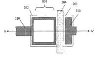
图1是显示根据本发明第一实施例的半导体器件的用于ESD保护的NMOS晶体管的平面示意图。1 is a schematic plan view showing an NMOS transistor for ESD protection of a semiconductor device according to a first embodiment of the present invention.
形成由n型重掺杂杂质区形成的源区201以及漏区202,以及在源区201和漏区202之间由绝缘膜例如氧化硅层等形成的栅绝缘膜(没有显示)上布置栅极204,从而形成用于ESD保护的NMOS晶体管。外部连接端区801在漏区202上方形成。直接位于外部连接端区801下方的第一金属连线310通过连接孔(没有显示)与用于ESD保护的NMOS晶体管的漏区202连接,以及延伸到内部区。此外,源区201以及栅极204的电位固定在地电位,采用所谓的截止晶体管的配置。A
在图1的实例中,外部连接端区801直接在用于ESD保护的NMOS晶体管的漏区202上方形成,以及在平面图中,形状为ESD保护元件区的一部分包括外部连接端。因此,本ESD保护元件可以在与常规方式相比更小的占用面积中形成。In the example of FIG. 1, the external
这里,外部连接端区801只在用于ESD保护的NMOS晶体管的漏区202上方形成以免与栅极204重叠。外部连接端区801是用于通过在测试过程或其他后续执行的过程中通过探测来进行电性测量,以及通过引线键合或其他类似方式来将IC芯片安装在封装树脂中的区域。此区域在探测或引线键合的过程中存在受到应力、拉伸、损伤或其他类似作用的风险。栅极204以及置于其下的栅绝缘膜是决定NMOS晶体管特性的主要部分,并且对机械应力极其敏感以及易受损伤。在本发明中,外部连接端区801仅在漏区202上方提供,而不在栅极204上方,构成本发明的一项特征。Here, the
外部连接端区801在用于ESD保护的NMOS晶体管的漏区202上方形成,以及通过接触孔直接与漏区202连接。因为这个原因,外部连接端和ESD保护元件之间的电阻值与ESD保护元件和内部元件之间的电阻值相比变得相当地小。因此,ESD浪涌或静电脉冲可以被优先引导入保护元件一侧,以及利用向内部元件连线的电阻,快速和强静电脉冲可以不以其形式传送到内部元件,而以转变为缓慢和弱的信号的形式传送到内部元件。The external
图1的实施例说明用于ESD保护的NMOS晶体管的实例,其中栅极204沿外部连接端区801的一个方向(边)放置,但是本发明并没有被限制于此。栅极204可能沿外部连接端区801的两条边到四条边放置。The embodiment of FIG. 1 illustrates an example of an NMOS transistor for ESD protection, in which the
图2是沿第一实施例中图1的A-A’线的横截面示意图。Fig. 2 is a schematic cross-sectional view along line A-A' of Fig. 1 in the first embodiment.
由n型重掺杂杂质区形成的源区201和漏区202在p型硅衬底101上形成,以及p型硅衬底101位于源区201和漏区202之间的部分上,经过由例如氧化硅层等绝缘膜形成的栅绝缘膜203设置栅极204,从而形成用于ESD保护的NMOS晶体管。此外,作为元件隔离区的浅槽隔离区610在源区201和漏区202的外侧形成。A
这种情况下,源区201和栅极204的电位固定在地电位(没有显示)以采用所谓截止晶体管的配置。此外,在源区201和漏区202上方经过第一绝缘膜410形成由含有难熔金属的铝形成的第一金属连线310。在漏区202上形成的第一绝缘膜410中提供大量接触孔510以将第一金属连线310与漏区202电连接。在漏区202上形成的大量接触孔510几乎在整个漏区202上广泛分布以及放置。这是因为如果用于ESD保护的NMOS晶体管起作用以接收ESD浪涌以及通过双极运行放出电流,避免了此运行在局部范围内进行。In this case, the potentials of the
由于用于ESD保护的NMOS晶体管为了执行保护功能必须处理大电流,因此分配宽的沟道宽度W。然而,如果例如在局部提供接触孔510,充分利用大的沟道宽度是不可能的,以及运行被限制在局部区。在某些情况下,大电流局部集中会造成击穿,由此不能发挥出期望的ESD耐受能力。这种整个漏区202上广泛分布以及密集放置大量接触孔510使得用于ESD保护710的NMOS晶体管能够整体上均匀运行抵抗到来的静电脉冲,通过整个沟道宽度使静电脉冲能够得到有效处理(释放)。Since an NMOS transistor for ESD protection must handle a large current in order to perform a protection function, a wide channel width W is allocated. However, if, for example, the
与漏区202连接的第一金属连线310在漏区202上方形成外部连接端区801,以及延伸到内部区。此外,源区201通过接触孔510连接到第一金属连线310,以及与栅极204一起被固定在地电位(没有显示)。由氮化硅膜或类似形成的保护膜440在第一金属连线310上形成,以及保护层440在漏区202上方的部分被去除,由此形成其中第一金属连线310成暴露的外部连接端区801。如此,外部连接端区801直接在用于ESD保护的NMOS晶体管的漏区202上方形成。之前在图1的说明中给出了这样形成的原因以及其效果。The
(第二实施例)(second embodiment)
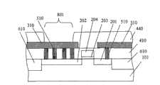
图3是显示根据本发明第二实施例的半导体器件的用于ESD保护的NMOS晶体管的平面示意图。3 is a schematic plan view showing an NMOS transistor for ESD protection of a semiconductor device according to a second embodiment of the present invention.
由n型重掺杂杂质区形成的漏区202具有由栅极204界定的大致上的圆周,以及其平面形状经过栅极204被源区201包围。栅极204放置在介于漏区202和源区201之间在由例如氧化硅薄膜等绝缘薄膜形成的栅绝缘膜(没有显示)上,从而形成用于ESD保护的NMOS晶体管。第一金属连线310放置在漏区202上方,通过接触孔(没有显示)与用于ESD保护的NMOS晶体管的漏区202连接,以及延伸到内部区。The
此外,第一金属连线310通过通孔(没有显示)在漏区202上方与第二金属连线320连接,以及形成外部连接端区801。源区201以及栅极204的电位固定在地电位,以及采取所谓的截止晶体管的配置。在这种情况下,漏区202具有由栅极204界定的大致上的圆周,以及其平面形状经过栅极204被源区201包围。上述的原因是为了将漏区202与元件隔离区分开,以及避免形成电流在其处集中的转角。In addition, the
一般而言,当采用浅槽隔离作为元件隔离时,在很多情况下,由晶体缺陷或类似问题造成的漏电流会在接近另外的元件的部分产生。特别地对于具有宽晶体管宽度W的用于ESD保护的NMOS晶体管这很可能会变成严重的问题。In general, when shallow trench isolation is used as element isolation, leakage current due to crystal defects or the like occurs in parts close to another element in many cases. This is likely to become a serious problem especially for NMOS transistors for ESD protection with wide transistor width W.
在本发明中,用于ESD保护的NMOS晶体管的漏区与元件隔离区相互分开,以及源区经过栅极完全包围漏区,由此可以防止特别在浅槽隔离中会成为问题的漏电流增大。再者,由于漏区的平面形状不具有转角,可以防止由于电流集中造成局部击穿从而保证足够的ESD耐受能力抵抗到来的电涌。In the present invention, the drain region and the element isolation region of the NMOS transistor used for ESD protection are separated from each other, and the source region completely surrounds the drain region through the gate, thereby preventing an increase in leakage current that would be a problem particularly in shallow trench isolation. big. Furthermore, since the planar shape of the drain region has no corners, local breakdown due to current concentration can be prevented to ensure sufficient ESD withstand capability against incoming surges.
在图3示出的第二实施例中,漏区202具有大致上圆形。然而,这里的目的是消除电流集中,以及因此漏区202可以是大致上椭圆的形状,或者可以是其中转角部分为圆形的大致上矩形的形状。此外,已经说明了外部连接端区801具有矩形的情况,但外部连接端区801可能具有与漏区202一致的大致上圆形的形状。考虑到后续的探测或类似步骤,存在一种情况,从保证关于按所有方向探测的位移有相等边际的角度来看,环形比矩形好。接触孔以及通孔也需要根据外部连接端区801的形状广泛分布以及放置。In the second embodiment shown in FIG. 3, the
同样在图3示出的第二实施例中,如同在图1示出的第一实施例中,外部连接端区801直接在用于ESD保护的NMOS晶体管的漏区202上方形成,以及在平面图中,其形状中ESD保护元件区的一部分包括外部连接端。因为这个原因,ESD保护元件可以在与常规方式相比更小的占用面积中形成。此外,同样在这个实施例中,如同第一实施例,外部连接端区801仅在用于ESD保护的NMOS晶体管的漏区202上方形成以便不与栅极204重叠。上述的原因以及它的说明与图1示出的第一实施例的相似。Also in the second embodiment shown in FIG. 3, as in the first embodiment shown in FIG. 1, the external
在图3示出的第二实施例中,外部连接端区801由直接在用于ESD保护的NMOS晶体管的漏区202上方形成的第二金属连线320形成。在这种情况下,说明用于形成半导体器件而采用多层连线的例子,以及本发明并不限于两层金属连线。在第二实施例中,外部连接端区801在用于ESD保护的NMOS晶体管的漏区202上方形成,以及通过通孔和接触孔直接与漏区202连接。因为这个原因,外部连接端和ESD保护元件之间的电阻值与ESD保护元件和内部元件之间的电阻值相比变得相当地小。因此,ESD浪涌或静电脉冲可以被优先引导入保护元件一侧。而且,利用例如向内部元件连线的电阻,快速和强静电脉冲不以它本身形式传送到内部元件,而可以在传输到内部元件前转变为缓慢和弱的信号。In the second embodiment shown in FIG. 3 , the external
图4是沿第二实施例中图3的B-B’线的横截面示意图。Fig. 4 is a schematic cross-sectional view along line B-B' of Fig. 3 in the second embodiment.
由n型重掺杂杂质区形成的源区201和漏区202在p型硅衬底101上形成,以及在p型硅衬底101位于源区201和漏区202之间的部分上经过由例如氧化硅膜等绝缘膜形成的栅绝缘膜203设置栅极204,从而形成用于ESD保护的NMOS晶体管。这里,源区201经过P型硅衬底101用作NMOS晶体管沟道区的部分包围漏区202的外围。此外,用作元件隔离区的浅槽隔离区610在源区201和漏区202的外侧形成。A
这种情况下,源区201和栅极204的电位固定在地电位(没有显示)以具有所谓截止晶体管的配置。此外,在源区201和漏区202上方经过第一绝缘膜410形成由含有难熔金属的铝形成的第一金属连线310。在漏区202上形成的第一绝缘膜410中提供大量接触孔510以将第一金属连线310与漏区202电连接。此外,在漏区202上形成的大量接触孔510几乎在整个漏区202上广泛分布以及密集放置,以防止用于ESD保护710的NMOS晶体管在捕捉ESD浪涌并通过双极运行释放电流的过程中局部以及部分运行。In this case, the potentials of the
由于用于ESD保护的NMOS晶体管为了执行保护功能必须处理大电流,因此分配宽的沟道宽度W。然而,如果例如局部提供接触孔510,充分利用大的沟道宽度是不可能的,以及运行被限制在局部区。在某些情况下,大电流局部集中会造成击穿,由此不能发挥出期望的ESD耐受能力。这种整个漏区202上广泛分布以及密集放置大量接触孔510使得用于ESD保护710的NMOS晶体管能够整体上均匀运行抵抗到来的静电脉冲,通过整个沟道宽度使静电脉冲能够得到有效处理(释放)。Since an NMOS transistor for ESD protection must handle a large current in order to perform a protection function, a wide channel width W is allocated. However, if, for example, the
在位于漏区202上方的第一金属连线310上方经过第二绝缘膜420形成由例如含有难熔金属的铝形成的第二金属连线320,以及通过大量通孔520与第一金属连线310连接。与漏区202连接的第一金属连线310通过通孔在漏区202上方与第二金属连线320连接以形成外部连接端区801,以及延伸到内部区域。此外,源区201通过接触孔510连接到第一金属连线310,以及与栅极204一起被固定在地电位(没有显示)。由氮化硅膜或类似形成的保护膜440在第二金属连线320周围形成,以及保护层440在漏区202上方的部分被去除,由此形成外部连接端区801,其中第二金属连线310成暴露的。A
如此,外部连接端区801直接在用于ESD保护的NMOS晶体管的漏区202上方形成。这样形成的原因以及其效果与图1以及图2的相似。As such, the external
如上述说明的,根据本发明,用于ESD保护的NMOS晶体管可以在小的占用面积中形成。而且,可以将静电脉冲最可能的部分引导入截止晶体管从而不会传导到内部元件以阻止内部元件被ESD击穿,或者在传输前可以将快速和强静电脉冲转变为缓慢和弱的信号。因此,获得包括能够执行充分的ESD保护功能而占用面积小的ESD保护元件的半导体器件是可能的。As explained above, according to the present invention, an NMOS transistor for ESD protection can be formed in a small footprint. Furthermore, it is possible to direct the most probable part of the static pulse into the blocking transistor so that it does not conduct to the internal components to prevent the internal components from being broken down by ESD, or to convert the fast and strong static pulse into a slow and weak signal before transmission. Therefore, it is possible to obtain a semiconductor device including an ESD protection element capable of performing a sufficient ESD protection function while occupying a small area.
Claims (6)
Translated fromChineseApplications Claiming Priority (3)
| Application Number | Priority Date | Filing Date | Title |
|---|---|---|---|
| JP2007320973 | 2007-12-12 | ||
| JP2007-320973 | 2007-12-12 | ||
| JP2007320973AJP2009147001A (en) | 2007-12-12 | 2007-12-12 | Semiconductor device |
Publications (2)
| Publication Number | Publication Date |
|---|---|
| CN101459176A CN101459176A (en) | 2009-06-17 |
| CN101459176Btrue CN101459176B (en) | 2013-01-23 |
Family
ID=40752066
Family Applications (1)
| Application Number | Title | Priority Date | Filing Date |
|---|---|---|---|
| CN200810187029XAExpired - Fee RelatedCN101459176B (en) | 2007-12-12 | 2008-12-12 | Semiconductor device with a plurality of transistors |
Country Status (4)
| Country | Link |
|---|---|
| US (1) | US7898035B2 (en) |
| JP (1) | JP2009147001A (en) |
| KR (1) | KR101489003B1 (en) |
| CN (1) | CN101459176B (en) |
Families Citing this family (5)
| Publication number | Priority date | Publication date | Assignee | Title |
|---|---|---|---|---|
| JP2009147001A (en)* | 2007-12-12 | 2009-07-02 | Seiko Instruments Inc | Semiconductor device |
| US8378422B2 (en)* | 2009-02-06 | 2013-02-19 | Taiwan Semiconductor Manufacturing Company, Ltd. | Electrostatic discharge protection device comprising a plurality of highly doped areas within a well |
| JP2011071329A (en)* | 2009-09-25 | 2011-04-07 | Seiko Instruments Inc | Semiconductor device |
| JP5546191B2 (en)* | 2009-09-25 | 2014-07-09 | セイコーインスツル株式会社 | Semiconductor device |
| US12396267B2 (en)* | 2023-02-02 | 2025-08-19 | Vanguard International Semiconductor Corporation | Semiconductor device |
Citations (1)
| Publication number | Priority date | Publication date | Assignee | Title |
|---|---|---|---|---|
| US5910675A (en)* | 1995-12-14 | 1999-06-08 | Nec Corporation | Semiconductor device and method of making the same |
Family Cites Families (12)
| Publication number | Priority date | Publication date | Assignee | Title |
|---|---|---|---|---|
| JP2642000B2 (en)* | 1991-05-21 | 1997-08-20 | 日本電気アイシーマイコンシステム株式会社 | MOS integrated circuit device |
| JP3203831B2 (en)* | 1992-10-23 | 2001-08-27 | ソニー株式会社 | ESD protection transistor |
| JP2003289104A (en)* | 2002-03-28 | 2003-10-10 | Ricoh Co Ltd | Semiconductor device protection circuit and semiconductor device |
| JP2005019452A (en)* | 2003-06-23 | 2005-01-20 | Toshiba Corp | Semiconductor device |
| US6940131B2 (en)* | 2003-06-30 | 2005-09-06 | Texas Instruments Incorporated | MOS ESD CDM clamp with integral substrate injection guardring and method for fabrication |
| JP4593094B2 (en)* | 2003-08-21 | 2010-12-08 | 日本電気株式会社 | Liquid crystal display device and manufacturing method thereof |
| US6943069B2 (en)* | 2003-10-14 | 2005-09-13 | Semiconductor Components Industries, L.L.C. | Power system inhibit method and device and structure therefor |
| KR20050035687A (en)* | 2003-10-14 | 2005-04-19 | 삼성전자주식회사 | Elector static discharge protection device and manufacturing method thereof |
| US20050224883A1 (en)* | 2004-04-06 | 2005-10-13 | Taiwan Semiconductor Manufacturing Company, Ltd. | Circuit design for increasing charge device model immunity |
| US7397089B2 (en)* | 2005-08-10 | 2008-07-08 | Skyworks Solutions, Inc. | ESD protection structure using contact-via chains as ballast resistors |
| JP5586819B2 (en)* | 2006-04-06 | 2014-09-10 | ピーエスフォー ルクスコ エスエイアールエル | Semiconductor device |
| JP2009147001A (en)* | 2007-12-12 | 2009-07-02 | Seiko Instruments Inc | Semiconductor device |
- 2007
- 2007-12-12JPJP2007320973Apatent/JP2009147001A/ennot_activeWithdrawn
- 2008
- 2008-12-04USUS12/315,635patent/US7898035B2/ennot_activeExpired - Fee Related
- 2008-12-12CNCN200810187029XApatent/CN101459176B/ennot_activeExpired - Fee Related
- 2008-12-12KRKR20080126300Apatent/KR101489003B1/ennot_activeExpired - Fee Related
Patent Citations (1)
| Publication number | Priority date | Publication date | Assignee | Title |
|---|---|---|---|---|
| US5910675A (en)* | 1995-12-14 | 1999-06-08 | Nec Corporation | Semiconductor device and method of making the same |
Also Published As
| Publication number | Publication date |
|---|---|
| US20090152633A1 (en) | 2009-06-18 |
| US7898035B2 (en) | 2011-03-01 |
| CN101459176A (en) | 2009-06-17 |
| KR20090063149A (en) | 2009-06-17 |
| JP2009147001A (en) | 2009-07-02 |
| KR101489003B1 (en) | 2015-02-02 |
Similar Documents
| Publication | Publication Date | Title |
|---|---|---|
| US11189611B2 (en) | Electrostatic discharge protection semiconductor device | |
| KR910009355B1 (en) | Input protection circuit of MOS semiconductor device | |
| JPH11274404A (en) | Semiconductor device | |
| CN101221952A (en) | Semiconductor structure for protecting an internal integrated circuit and its manufacturing method | |
| KR20090020528A (en) | Semiconductor devices | |
| US8207581B2 (en) | Semiconductor device | |
| CN101459176B (en) | Semiconductor device with a plurality of transistors | |
| US20110163384A1 (en) | Semiconductor device | |
| CN101236967A (en) | A silicon controlled rectifier embedded in an inverter | |
| JP3792931B2 (en) | Semiconductor device and test method thereof | |
| US5401997A (en) | ESD protection for poly resistor on oxide | |
| CN1324705C (en) | Integrated circuits that avoid latch-up | |
| KR100638455B1 (en) | ESD protection circuit for high voltage device and semiconductor device having same | |
| CN204792800U (en) | Power transistors with high-efficiency ESD protection | |
| JP4006023B2 (en) | Integrated circuit | |
| JP3214457B2 (en) | Method for manufacturing semiconductor device | |
| KR20210042246A (en) | Electrostatic discharge handling for sense igbt using zener diode | |
| JPS63291470A (en) | Protective circuit for semiconductor integrated circuit device | |
| KR20050071023A (en) | Gate grounded nmos transistor for protection against the electrostatic discharge | |
| KR101369194B1 (en) | Esd protection circuit for semiconductor integrated circuit | |
| JP2011192842A (en) | Semiconductor device | |
| JPH04145658A (en) | Semiconductor integrated circuit | |
| CN115084125A (en) | Electrostatic protection circuit and semiconductor device | |
| JPH1140746A (en) | Surge protection circuit device and semiconductor element structure used therein | |
| JPH0777235B2 (en) | Semiconductor input protection device |
Legal Events
| Date | Code | Title | Description |
|---|---|---|---|
| C06 | Publication | ||
| PB01 | Publication | ||
| C10 | Entry into substantive examination | ||
| SE01 | Entry into force of request for substantive examination | ||
| C14 | Grant of patent or utility model | ||
| GR01 | Patent grant | ||
| C41 | Transfer of patent application or patent right or utility model | ||
| TR01 | Transfer of patent right | Effective date of registration:20160323 Address after:Chiba County, Japan Patentee after:SEIKO INSTR INC Address before:Chiba, Chiba, Japan Patentee before:Seiko Instruments Inc. | |
| CP01 | Change in the name or title of a patent holder | Address after:Chiba County, Japan Patentee after:EPPs Lingke Co. Ltd. Address before:Chiba County, Japan Patentee before:SEIKO INSTR INC | |
| CP01 | Change in the name or title of a patent holder | ||
| CF01 | Termination of patent right due to non-payment of annual fee | Granted publication date:20130123 Termination date:20201212 | |
| CF01 | Termination of patent right due to non-payment of annual fee |