CN101459155A - Circuit board having bypass pad - Google Patents
Circuit board having bypass padDownload PDFInfo
- Publication number
- CN101459155A CN101459155ACNA200810179478XACN200810179478ACN101459155ACN 101459155 ACN101459155 ACN 101459155ACN A200810179478X ACNA200810179478X ACN A200810179478XACN 200810179478 ACN200810179478 ACN 200810179478ACN 101459155 ACN101459155 ACN 101459155A
- Authority
- CN
- China
- Prior art keywords
- pcb
- pad
- bypass
- circuit board
- printed circuit
- Prior art date
- Legal status (The legal status is an assumption and is not a legal conclusion. Google has not performed a legal analysis and makes no representation as to the accuracy of the status listed.)
- Granted
Links
Images


Classifications
- H—ELECTRICITY
- H01—ELECTRIC ELEMENTS
- H01L—SEMICONDUCTOR DEVICES NOT COVERED BY CLASS H10
- H01L25/00—Assemblies consisting of a plurality of semiconductor or other solid state devices
- H01L25/03—Assemblies consisting of a plurality of semiconductor or other solid state devices all the devices being of a type provided for in a single subclass of subclasses H10B, H10D, H10F, H10H, H10K or H10N, e.g. assemblies of rectifier diodes
- H01L25/04—Assemblies consisting of a plurality of semiconductor or other solid state devices all the devices being of a type provided for in a single subclass of subclasses H10B, H10D, H10F, H10H, H10K or H10N, e.g. assemblies of rectifier diodes the devices not having separate containers
- H01L25/065—Assemblies consisting of a plurality of semiconductor or other solid state devices all the devices being of a type provided for in a single subclass of subclasses H10B, H10D, H10F, H10H, H10K or H10N, e.g. assemblies of rectifier diodes the devices not having separate containers the devices being of a type provided for in group H10D89/00
- H01L25/0657—Stacked arrangements of devices
- H—ELECTRICITY
- H01—ELECTRIC ELEMENTS
- H01L—SEMICONDUCTOR DEVICES NOT COVERED BY CLASS H10
- H01L23/00—Details of semiconductor or other solid state devices
- H01L23/12—Mountings, e.g. non-detachable insulating substrates
- G—PHYSICS
- G01—MEASURING; TESTING
- G01R—MEASURING ELECTRIC VARIABLES; MEASURING MAGNETIC VARIABLES
- G01R31/00—Arrangements for testing electric properties; Arrangements for locating electric faults; Arrangements for electrical testing characterised by what is being tested not provided for elsewhere
- G01R31/28—Testing of electronic circuits, e.g. by signal tracer
- G01R31/2801—Testing of printed circuits, backplanes, motherboards, hybrid circuits or carriers for multichip packages [MCP]
- G01R31/2806—Apparatus therefor, e.g. test stations, drivers, analysers, conveyors
- G01R31/2808—Holding, conveying or contacting devices, e.g. test adapters, edge connectors, extender boards
- G—PHYSICS
- G01—MEASURING; TESTING
- G01R—MEASURING ELECTRIC VARIABLES; MEASURING MAGNETIC VARIABLES
- G01R31/00—Arrangements for testing electric properties; Arrangements for locating electric faults; Arrangements for electrical testing characterised by what is being tested not provided for elsewhere
- G01R31/28—Testing of electronic circuits, e.g. by signal tracer
- G01R31/2801—Testing of printed circuits, backplanes, motherboards, hybrid circuits or carriers for multichip packages [MCP]
- G01R31/2818—Testing of printed circuits, backplanes, motherboards, hybrid circuits or carriers for multichip packages [MCP] using test structures on, or modifications of, the card under test, made for the purpose of testing, e.g. additional components or connectors
- G—PHYSICS
- G11—INFORMATION STORAGE
- G11C—STATIC STORES
- G11C29/00—Checking stores for correct operation ; Subsequent repair; Testing stores during standby or offline operation
- G11C29/04—Detection or location of defective memory elements, e.g. cell constructio details, timing of test signals
- G—PHYSICS
- G11—INFORMATION STORAGE
- G11C—STATIC STORES
- G11C29/00—Checking stores for correct operation ; Subsequent repair; Testing stores during standby or offline operation
- G11C29/04—Detection or location of defective memory elements, e.g. cell constructio details, timing of test signals
- G11C29/08—Functional testing, e.g. testing during refresh, power-on self testing [POST] or distributed testing
- G11C29/12—Built-in arrangements for testing, e.g. built-in self testing [BIST] or interconnection details
- G—PHYSICS
- G11—INFORMATION STORAGE
- G11C—STATIC STORES
- G11C29/00—Checking stores for correct operation ; Subsequent repair; Testing stores during standby or offline operation
- G11C29/56—External testing equipment for static stores, e.g. automatic test equipment [ATE]; Interfaces therefor
- G—PHYSICS
- G11—INFORMATION STORAGE
- G11C—STATIC STORES
- G11C29/00—Checking stores for correct operation ; Subsequent repair; Testing stores during standby or offline operation
- G11C29/56—External testing equipment for static stores, e.g. automatic test equipment [ATE]; Interfaces therefor
- G11C29/56016—Apparatus features
- G—PHYSICS
- G11—INFORMATION STORAGE
- G11C—STATIC STORES
- G11C5/00—Details of stores covered by group G11C11/00
- G11C5/02—Disposition of storage elements, e.g. in the form of a matrix array
- G—PHYSICS
- G11—INFORMATION STORAGE
- G11C—STATIC STORES
- G11C5/00—Details of stores covered by group G11C11/00
- G11C5/02—Disposition of storage elements, e.g. in the form of a matrix array
- G11C5/025—Geometric lay-out considerations of storage- and peripheral-blocks in a semiconductor storage device
- G—PHYSICS
- G11—INFORMATION STORAGE
- G11C—STATIC STORES
- G11C5/00—Details of stores covered by group G11C11/00
- G11C5/06—Arrangements for interconnecting storage elements electrically, e.g. by wiring
- H—ELECTRICITY
- H01—ELECTRIC ELEMENTS
- H01L—SEMICONDUCTOR DEVICES NOT COVERED BY CLASS H10
- H01L22/00—Testing or measuring during manufacture or treatment; Reliability measurements, i.e. testing of parts without further processing to modify the parts as such; Structural arrangements therefor
- H01L22/30—Structural arrangements specially adapted for testing or measuring during manufacture or treatment, or specially adapted for reliability measurements
- H01L22/32—Additional lead-in metallisation on a device or substrate, e.g. additional pads or pad portions, lines in the scribe line, sacrificed conductors
- H—ELECTRICITY
- H01—ELECTRIC ELEMENTS
- H01L—SEMICONDUCTOR DEVICES NOT COVERED BY CLASS H10
- H01L23/00—Details of semiconductor or other solid state devices
- H01L23/48—Arrangements for conducting electric current to or from the solid state body in operation, e.g. leads, terminal arrangements ; Selection of materials therefor
- H01L23/488—Arrangements for conducting electric current to or from the solid state body in operation, e.g. leads, terminal arrangements ; Selection of materials therefor consisting of soldered or bonded constructions
- H01L23/498—Leads, i.e. metallisations or lead-frames on insulating substrates, e.g. chip carriers
- H01L23/49811—Additional leads joined to the metallisation on the insulating substrate, e.g. pins, bumps, wires, flat leads
- H—ELECTRICITY
- H01—ELECTRIC ELEMENTS
- H01L—SEMICONDUCTOR DEVICES NOT COVERED BY CLASS H10
- H01L23/00—Details of semiconductor or other solid state devices
- H01L23/48—Arrangements for conducting electric current to or from the solid state body in operation, e.g. leads, terminal arrangements ; Selection of materials therefor
- H01L23/488—Arrangements for conducting electric current to or from the solid state body in operation, e.g. leads, terminal arrangements ; Selection of materials therefor consisting of soldered or bonded constructions
- H01L23/498—Leads, i.e. metallisations or lead-frames on insulating substrates, e.g. chip carriers
- H01L23/49838—Geometry or layout
- H—ELECTRICITY
- H01—ELECTRIC ELEMENTS
- H01L—SEMICONDUCTOR DEVICES NOT COVERED BY CLASS H10
- H01L23/00—Details of semiconductor or other solid state devices
- H01L23/52—Arrangements for conducting electric current within the device in operation from one component to another, i.e. interconnections, e.g. wires, lead frames
- H01L23/538—Arrangements for conducting electric current within the device in operation from one component to another, i.e. interconnections, e.g. wires, lead frames the interconnection structure between a plurality of semiconductor chips being formed on, or in, insulating substrates
- H—ELECTRICITY
- H01—ELECTRIC ELEMENTS
- H01L—SEMICONDUCTOR DEVICES NOT COVERED BY CLASS H10
- H01L24/00—Arrangements for connecting or disconnecting semiconductor or solid-state bodies; Methods or apparatus related thereto
- H01L24/01—Means for bonding being attached to, or being formed on, the surface to be connected, e.g. chip-to-package, die-attach, "first-level" interconnects; Manufacturing methods related thereto
- H01L24/02—Bonding areas ; Manufacturing methods related thereto
- H01L24/07—Structure, shape, material or disposition of the bonding areas after the connecting process
- H01L24/09—Structure, shape, material or disposition of the bonding areas after the connecting process of a plurality of bonding areas
- H—ELECTRICITY
- H01—ELECTRIC ELEMENTS
- H01L—SEMICONDUCTOR DEVICES NOT COVERED BY CLASS H10
- H01L24/00—Arrangements for connecting or disconnecting semiconductor or solid-state bodies; Methods or apparatus related thereto
- H01L24/01—Means for bonding being attached to, or being formed on, the surface to be connected, e.g. chip-to-package, die-attach, "first-level" interconnects; Manufacturing methods related thereto
- H01L24/42—Wire connectors; Manufacturing methods related thereto
- H01L24/47—Structure, shape, material or disposition of the wire connectors after the connecting process
- H01L24/49—Structure, shape, material or disposition of the wire connectors after the connecting process of a plurality of wire connectors
- H—ELECTRICITY
- H01—ELECTRIC ELEMENTS
- H01L—SEMICONDUCTOR DEVICES NOT COVERED BY CLASS H10
- H01L24/00—Arrangements for connecting or disconnecting semiconductor or solid-state bodies; Methods or apparatus related thereto
- H01L24/80—Methods for connecting semiconductor or other solid state bodies using means for bonding being attached to, or being formed on, the surface to be connected
- H—ELECTRICITY
- H01—ELECTRIC ELEMENTS
- H01L—SEMICONDUCTOR DEVICES NOT COVERED BY CLASS H10
- H01L25/00—Assemblies consisting of a plurality of semiconductor or other solid state devices
- H01L25/18—Assemblies consisting of a plurality of semiconductor or other solid state devices the devices being of the types provided for in two or more different main groups of the same subclass of H10B, H10D, H10F, H10H, H10K or H10N
- H—ELECTRICITY
- H05—ELECTRIC TECHNIQUES NOT OTHERWISE PROVIDED FOR
- H05K—PRINTED CIRCUITS; CASINGS OR CONSTRUCTIONAL DETAILS OF ELECTRIC APPARATUS; MANUFACTURE OF ASSEMBLAGES OF ELECTRICAL COMPONENTS
- H05K1/00—Printed circuits
- H05K1/02—Details
- H—ELECTRICITY
- H05—ELECTRIC TECHNIQUES NOT OTHERWISE PROVIDED FOR
- H05K—PRINTED CIRCUITS; CASINGS OR CONSTRUCTIONAL DETAILS OF ELECTRIC APPARATUS; MANUFACTURE OF ASSEMBLAGES OF ELECTRICAL COMPONENTS
- H05K1/00—Printed circuits
- H05K1/02—Details
- H05K1/0266—Marks, test patterns or identification means
- H05K1/0268—Marks, test patterns or identification means for electrical inspection or testing
- H—ELECTRICITY
- H05—ELECTRIC TECHNIQUES NOT OTHERWISE PROVIDED FOR
- H05K—PRINTED CIRCUITS; CASINGS OR CONSTRUCTIONAL DETAILS OF ELECTRIC APPARATUS; MANUFACTURE OF ASSEMBLAGES OF ELECTRICAL COMPONENTS
- H05K1/00—Printed circuits
- H05K1/02—Details
- H05K1/11—Printed elements for providing electric connections to or between printed circuits
- H05K1/111—Pads for surface mounting, e.g. lay-out
- H—ELECTRICITY
- H05—ELECTRIC TECHNIQUES NOT OTHERWISE PROVIDED FOR
- H05K—PRINTED CIRCUITS; CASINGS OR CONSTRUCTIONAL DETAILS OF ELECTRIC APPARATUS; MANUFACTURE OF ASSEMBLAGES OF ELECTRICAL COMPONENTS
- H05K1/00—Printed circuits
- H05K1/18—Printed circuits structurally associated with non-printed electric components
- H05K1/181—Printed circuits structurally associated with non-printed electric components associated with surface mounted components
- H—ELECTRICITY
- H05—ELECTRIC TECHNIQUES NOT OTHERWISE PROVIDED FOR
- H05K—PRINTED CIRCUITS; CASINGS OR CONSTRUCTIONAL DETAILS OF ELECTRIC APPARATUS; MANUFACTURE OF ASSEMBLAGES OF ELECTRICAL COMPONENTS
- H05K3/00—Apparatus or processes for manufacturing printed circuits
- H05K3/22—Secondary treatment of printed circuits
- H05K3/28—Applying non-metallic protective coatings
- H05K3/288—Removal of non-metallic coatings, e.g. for repairing
- G—PHYSICS
- G11—INFORMATION STORAGE
- G11C—STATIC STORES
- G11C29/00—Checking stores for correct operation ; Subsequent repair; Testing stores during standby or offline operation
- G11C29/56—External testing equipment for static stores, e.g. automatic test equipment [ATE]; Interfaces therefor
- G11C2029/5602—Interface to device under test
- H—ELECTRICITY
- H01—ELECTRIC ELEMENTS
- H01L—SEMICONDUCTOR DEVICES NOT COVERED BY CLASS H10
- H01L2224/00—Indexing scheme for arrangements for connecting or disconnecting semiconductor or solid-state bodies and methods related thereto as covered by H01L24/00
- H01L2224/01—Means for bonding being attached to, or being formed on, the surface to be connected, e.g. chip-to-package, die-attach, "first-level" interconnects; Manufacturing methods related thereto
- H01L2224/02—Bonding areas; Manufacturing methods related thereto
- H01L2224/04—Structure, shape, material or disposition of the bonding areas prior to the connecting process
- H01L2224/05—Structure, shape, material or disposition of the bonding areas prior to the connecting process of an individual bonding area
- H01L2224/0554—External layer
- H01L2224/0555—Shape
- H01L2224/05552—Shape in top view
- H01L2224/05554—Shape in top view being square
- H—ELECTRICITY
- H01—ELECTRIC ELEMENTS
- H01L—SEMICONDUCTOR DEVICES NOT COVERED BY CLASS H10
- H01L2224/00—Indexing scheme for arrangements for connecting or disconnecting semiconductor or solid-state bodies and methods related thereto as covered by H01L24/00
- H01L2224/01—Means for bonding being attached to, or being formed on, the surface to be connected, e.g. chip-to-package, die-attach, "first-level" interconnects; Manufacturing methods related thereto
- H01L2224/02—Bonding areas; Manufacturing methods related thereto
- H01L2224/04—Structure, shape, material or disposition of the bonding areas prior to the connecting process
- H01L2224/06—Structure, shape, material or disposition of the bonding areas prior to the connecting process of a plurality of bonding areas
- H01L2224/0601—Structure
- H01L2224/0603—Bonding areas having different sizes, e.g. different heights or widths
- H—ELECTRICITY
- H01—ELECTRIC ELEMENTS
- H01L—SEMICONDUCTOR DEVICES NOT COVERED BY CLASS H10
- H01L2224/00—Indexing scheme for arrangements for connecting or disconnecting semiconductor or solid-state bodies and methods related thereto as covered by H01L24/00
- H01L2224/01—Means for bonding being attached to, or being formed on, the surface to be connected, e.g. chip-to-package, die-attach, "first-level" interconnects; Manufacturing methods related thereto
- H01L2224/02—Bonding areas; Manufacturing methods related thereto
- H01L2224/07—Structure, shape, material or disposition of the bonding areas after the connecting process
- H01L2224/09—Structure, shape, material or disposition of the bonding areas after the connecting process of a plurality of bonding areas
- H01L2224/091—Disposition
- H01L2224/0912—Layout
- H—ELECTRICITY
- H01—ELECTRIC ELEMENTS
- H01L—SEMICONDUCTOR DEVICES NOT COVERED BY CLASS H10
- H01L2224/00—Indexing scheme for arrangements for connecting or disconnecting semiconductor or solid-state bodies and methods related thereto as covered by H01L24/00
- H01L2224/01—Means for bonding being attached to, or being formed on, the surface to be connected, e.g. chip-to-package, die-attach, "first-level" interconnects; Manufacturing methods related thereto
- H01L2224/42—Wire connectors; Manufacturing methods related thereto
- H01L2224/47—Structure, shape, material or disposition of the wire connectors after the connecting process
- H01L2224/48—Structure, shape, material or disposition of the wire connectors after the connecting process of an individual wire connector
- H01L2224/481—Disposition
- H01L2224/48135—Connecting between different semiconductor or solid-state bodies, i.e. chip-to-chip
- H01L2224/48145—Connecting between different semiconductor or solid-state bodies, i.e. chip-to-chip the bodies being stacked
- H—ELECTRICITY
- H01—ELECTRIC ELEMENTS
- H01L—SEMICONDUCTOR DEVICES NOT COVERED BY CLASS H10
- H01L2224/00—Indexing scheme for arrangements for connecting or disconnecting semiconductor or solid-state bodies and methods related thereto as covered by H01L24/00
- H01L2224/01—Means for bonding being attached to, or being formed on, the surface to be connected, e.g. chip-to-package, die-attach, "first-level" interconnects; Manufacturing methods related thereto
- H01L2224/42—Wire connectors; Manufacturing methods related thereto
- H01L2224/47—Structure, shape, material or disposition of the wire connectors after the connecting process
- H01L2224/48—Structure, shape, material or disposition of the wire connectors after the connecting process of an individual wire connector
- H01L2224/481—Disposition
- H01L2224/48151—Connecting between a semiconductor or solid-state body and an item not being a semiconductor or solid-state body, e.g. chip-to-substrate, chip-to-passive
- H01L2224/48221—Connecting between a semiconductor or solid-state body and an item not being a semiconductor or solid-state body, e.g. chip-to-substrate, chip-to-passive the body and the item being stacked
- H01L2224/48225—Connecting between a semiconductor or solid-state body and an item not being a semiconductor or solid-state body, e.g. chip-to-substrate, chip-to-passive the body and the item being stacked the item being non-metallic, e.g. insulating substrate with or without metallisation
- H01L2224/48227—Connecting between a semiconductor or solid-state body and an item not being a semiconductor or solid-state body, e.g. chip-to-substrate, chip-to-passive the body and the item being stacked the item being non-metallic, e.g. insulating substrate with or without metallisation connecting the wire to a bond pad of the item
- H—ELECTRICITY
- H01—ELECTRIC ELEMENTS
- H01L—SEMICONDUCTOR DEVICES NOT COVERED BY CLASS H10
- H01L2224/00—Indexing scheme for arrangements for connecting or disconnecting semiconductor or solid-state bodies and methods related thereto as covered by H01L24/00
- H01L2224/01—Means for bonding being attached to, or being formed on, the surface to be connected, e.g. chip-to-package, die-attach, "first-level" interconnects; Manufacturing methods related thereto
- H01L2224/42—Wire connectors; Manufacturing methods related thereto
- H01L2224/47—Structure, shape, material or disposition of the wire connectors after the connecting process
- H01L2224/49—Structure, shape, material or disposition of the wire connectors after the connecting process of a plurality of wire connectors
- H01L2224/491—Disposition
- H01L2224/4912—Layout
- H—ELECTRICITY
- H01—ELECTRIC ELEMENTS
- H01L—SEMICONDUCTOR DEVICES NOT COVERED BY CLASS H10
- H01L2225/00—Details relating to assemblies covered by the group H01L25/00 but not provided for in its subgroups
- H01L2225/03—All the devices being of a type provided for in the same main group of the same subclass of class H10, e.g. assemblies of rectifier diodes
- H01L2225/04—All the devices being of a type provided for in the same main group of the same subclass of class H10, e.g. assemblies of rectifier diodes the devices not having separate containers
- H01L2225/065—All the devices being of a type provided for in the same main group of the same subclass of class H10
- H01L2225/06503—Stacked arrangements of devices
- H01L2225/06506—Wire or wire-like electrical connections between devices
- H—ELECTRICITY
- H01—ELECTRIC ELEMENTS
- H01L—SEMICONDUCTOR DEVICES NOT COVERED BY CLASS H10
- H01L2225/00—Details relating to assemblies covered by the group H01L25/00 but not provided for in its subgroups
- H01L2225/03—All the devices being of a type provided for in the same main group of the same subclass of class H10, e.g. assemblies of rectifier diodes
- H01L2225/04—All the devices being of a type provided for in the same main group of the same subclass of class H10, e.g. assemblies of rectifier diodes the devices not having separate containers
- H01L2225/065—All the devices being of a type provided for in the same main group of the same subclass of class H10
- H01L2225/06503—Stacked arrangements of devices
- H01L2225/0651—Wire or wire-like electrical connections from device to substrate
- H—ELECTRICITY
- H01—ELECTRIC ELEMENTS
- H01L—SEMICONDUCTOR DEVICES NOT COVERED BY CLASS H10
- H01L2225/00—Details relating to assemblies covered by the group H01L25/00 but not provided for in its subgroups
- H01L2225/03—All the devices being of a type provided for in the same main group of the same subclass of class H10, e.g. assemblies of rectifier diodes
- H01L2225/04—All the devices being of a type provided for in the same main group of the same subclass of class H10, e.g. assemblies of rectifier diodes the devices not having separate containers
- H01L2225/065—All the devices being of a type provided for in the same main group of the same subclass of class H10
- H01L2225/06503—Stacked arrangements of devices
- H01L2225/06555—Geometry of the stack, e.g. form of the devices, geometry to facilitate stacking
- H01L2225/06562—Geometry of the stack, e.g. form of the devices, geometry to facilitate stacking at least one device in the stack being rotated or offset
- H—ELECTRICITY
- H01—ELECTRIC ELEMENTS
- H01L—SEMICONDUCTOR DEVICES NOT COVERED BY CLASS H10
- H01L2225/00—Details relating to assemblies covered by the group H01L25/00 but not provided for in its subgroups
- H01L2225/03—All the devices being of a type provided for in the same main group of the same subclass of class H10, e.g. assemblies of rectifier diodes
- H01L2225/04—All the devices being of a type provided for in the same main group of the same subclass of class H10, e.g. assemblies of rectifier diodes the devices not having separate containers
- H01L2225/065—All the devices being of a type provided for in the same main group of the same subclass of class H10
- H01L2225/06503—Stacked arrangements of devices
- H01L2225/06555—Geometry of the stack, e.g. form of the devices, geometry to facilitate stacking
- H01L2225/06568—Geometry of the stack, e.g. form of the devices, geometry to facilitate stacking the devices decreasing in size, e.g. pyramidical stack
- H—ELECTRICITY
- H01—ELECTRIC ELEMENTS
- H01L—SEMICONDUCTOR DEVICES NOT COVERED BY CLASS H10
- H01L2225/00—Details relating to assemblies covered by the group H01L25/00 but not provided for in its subgroups
- H01L2225/03—All the devices being of a type provided for in the same main group of the same subclass of class H10, e.g. assemblies of rectifier diodes
- H01L2225/04—All the devices being of a type provided for in the same main group of the same subclass of class H10, e.g. assemblies of rectifier diodes the devices not having separate containers
- H01L2225/065—All the devices being of a type provided for in the same main group of the same subclass of class H10
- H01L2225/06503—Stacked arrangements of devices
- H01L2225/06596—Structural arrangements for testing
- H—ELECTRICITY
- H01—ELECTRIC ELEMENTS
- H01L—SEMICONDUCTOR DEVICES NOT COVERED BY CLASS H10
- H01L24/00—Arrangements for connecting or disconnecting semiconductor or solid-state bodies; Methods or apparatus related thereto
- H01L24/01—Means for bonding being attached to, or being formed on, the surface to be connected, e.g. chip-to-package, die-attach, "first-level" interconnects; Manufacturing methods related thereto
- H01L24/42—Wire connectors; Manufacturing methods related thereto
- H01L24/47—Structure, shape, material or disposition of the wire connectors after the connecting process
- H01L24/48—Structure, shape, material or disposition of the wire connectors after the connecting process of an individual wire connector
- H—ELECTRICITY
- H01—ELECTRIC ELEMENTS
- H01L—SEMICONDUCTOR DEVICES NOT COVERED BY CLASS H10
- H01L25/00—Assemblies consisting of a plurality of semiconductor or other solid state devices
- H01L25/03—Assemblies consisting of a plurality of semiconductor or other solid state devices all the devices being of a type provided for in a single subclass of subclasses H10B, H10D, H10F, H10H, H10K or H10N, e.g. assemblies of rectifier diodes
- H01L25/04—Assemblies consisting of a plurality of semiconductor or other solid state devices all the devices being of a type provided for in a single subclass of subclasses H10B, H10D, H10F, H10H, H10K or H10N, e.g. assemblies of rectifier diodes the devices not having separate containers
- H01L25/065—Assemblies consisting of a plurality of semiconductor or other solid state devices all the devices being of a type provided for in a single subclass of subclasses H10B, H10D, H10F, H10H, H10K or H10N, e.g. assemblies of rectifier diodes the devices not having separate containers the devices being of a type provided for in group H10D89/00
- H01L25/0652—Assemblies consisting of a plurality of semiconductor or other solid state devices all the devices being of a type provided for in a single subclass of subclasses H10B, H10D, H10F, H10H, H10K or H10N, e.g. assemblies of rectifier diodes the devices not having separate containers the devices being of a type provided for in group H10D89/00 the devices being arranged next and on each other, i.e. mixed assemblies
- H—ELECTRICITY
- H01—ELECTRIC ELEMENTS
- H01L—SEMICONDUCTOR DEVICES NOT COVERED BY CLASS H10
- H01L25/00—Assemblies consisting of a plurality of semiconductor or other solid state devices
- H01L25/03—Assemblies consisting of a plurality of semiconductor or other solid state devices all the devices being of a type provided for in a single subclass of subclasses H10B, H10D, H10F, H10H, H10K or H10N, e.g. assemblies of rectifier diodes
- H01L25/04—Assemblies consisting of a plurality of semiconductor or other solid state devices all the devices being of a type provided for in a single subclass of subclasses H10B, H10D, H10F, H10H, H10K or H10N, e.g. assemblies of rectifier diodes the devices not having separate containers
- H01L25/065—Assemblies consisting of a plurality of semiconductor or other solid state devices all the devices being of a type provided for in a single subclass of subclasses H10B, H10D, H10F, H10H, H10K or H10N, e.g. assemblies of rectifier diodes the devices not having separate containers the devices being of a type provided for in group H10D89/00
- H01L25/0655—Assemblies consisting of a plurality of semiconductor or other solid state devices all the devices being of a type provided for in a single subclass of subclasses H10B, H10D, H10F, H10H, H10K or H10N, e.g. assemblies of rectifier diodes the devices not having separate containers the devices being of a type provided for in group H10D89/00 the devices being arranged next to each other
- H—ELECTRICITY
- H01—ELECTRIC ELEMENTS
- H01L—SEMICONDUCTOR DEVICES NOT COVERED BY CLASS H10
- H01L2924/00—Indexing scheme for arrangements or methods for connecting or disconnecting semiconductor or solid-state bodies as covered by H01L24/00
- H01L2924/0001—Technical content checked by a classifier
- H01L2924/00014—Technical content checked by a classifier the subject-matter covered by the group, the symbol of which is combined with the symbol of this group, being disclosed without further technical details
- H—ELECTRICITY
- H01—ELECTRIC ELEMENTS
- H01L—SEMICONDUCTOR DEVICES NOT COVERED BY CLASS H10
- H01L2924/00—Indexing scheme for arrangements or methods for connecting or disconnecting semiconductor or solid-state bodies as covered by H01L24/00
- H01L2924/01—Chemical elements
- H01L2924/01068—Erbium [Er]
- H—ELECTRICITY
- H01—ELECTRIC ELEMENTS
- H01L—SEMICONDUCTOR DEVICES NOT COVERED BY CLASS H10
- H01L2924/00—Indexing scheme for arrangements or methods for connecting or disconnecting semiconductor or solid-state bodies as covered by H01L24/00
- H01L2924/15—Details of package parts other than the semiconductor or other solid state devices to be connected
- H01L2924/181—Encapsulation
- H—ELECTRICITY
- H05—ELECTRIC TECHNIQUES NOT OTHERWISE PROVIDED FOR
- H05K—PRINTED CIRCUITS; CASINGS OR CONSTRUCTIONAL DETAILS OF ELECTRIC APPARATUS; MANUFACTURE OF ASSEMBLAGES OF ELECTRICAL COMPONENTS
- H05K1/00—Printed circuits
- H05K1/02—Details
- H05K1/11—Printed elements for providing electric connections to or between printed circuits
- H05K1/117—Pads along the edge of rigid circuit boards, e.g. for pluggable connectors
- H—ELECTRICITY
- H05—ELECTRIC TECHNIQUES NOT OTHERWISE PROVIDED FOR
- H05K—PRINTED CIRCUITS; CASINGS OR CONSTRUCTIONAL DETAILS OF ELECTRIC APPARATUS; MANUFACTURE OF ASSEMBLAGES OF ELECTRICAL COMPONENTS
- H05K2201/00—Indexing scheme relating to printed circuits covered by H05K1/00
- H05K2201/01—Dielectrics
- H05K2201/0183—Dielectric layers
- H05K2201/0187—Dielectric layers with regions of different dielectrics in the same layer, e.g. in a printed capacitor for locally changing the dielectric properties
- H—ELECTRICITY
- H05—ELECTRIC TECHNIQUES NOT OTHERWISE PROVIDED FOR
- H05K—PRINTED CIRCUITS; CASINGS OR CONSTRUCTIONAL DETAILS OF ELECTRIC APPARATUS; MANUFACTURE OF ASSEMBLAGES OF ELECTRICAL COMPONENTS
- H05K2201/00—Indexing scheme relating to printed circuits covered by H05K1/00
- H05K2201/03—Conductive materials
- H05K2201/0332—Structure of the conductor
- H05K2201/0335—Layered conductors or foils
- H05K2201/035—Paste overlayer, i.e. conductive paste or solder paste over conductive layer
- H—ELECTRICITY
- H05—ELECTRIC TECHNIQUES NOT OTHERWISE PROVIDED FOR
- H05K—PRINTED CIRCUITS; CASINGS OR CONSTRUCTIONAL DETAILS OF ELECTRIC APPARATUS; MANUFACTURE OF ASSEMBLAGES OF ELECTRICAL COMPONENTS
- H05K2201/00—Indexing scheme relating to printed circuits covered by H05K1/00
- H05K2201/09—Shape and layout
- H05K2201/09009—Substrate related
- H05K2201/09036—Recesses or grooves in insulating substrate
- H—ELECTRICITY
- H05—ELECTRIC TECHNIQUES NOT OTHERWISE PROVIDED FOR
- H05K—PRINTED CIRCUITS; CASINGS OR CONSTRUCTIONAL DETAILS OF ELECTRIC APPARATUS; MANUFACTURE OF ASSEMBLAGES OF ELECTRICAL COMPONENTS
- H05K2201/00—Indexing scheme relating to printed circuits covered by H05K1/00
- H05K2201/09—Shape and layout
- H05K2201/09209—Shape and layout details of conductors
- H05K2201/09372—Pads and lands
- H05K2201/09472—Recessed pad for surface mounting; Recessed electrode of component
- H—ELECTRICITY
- H05—ELECTRIC TECHNIQUES NOT OTHERWISE PROVIDED FOR
- H05K—PRINTED CIRCUITS; CASINGS OR CONSTRUCTIONAL DETAILS OF ELECTRIC APPARATUS; MANUFACTURE OF ASSEMBLAGES OF ELECTRICAL COMPONENTS
- H05K2201/00—Indexing scheme relating to printed circuits covered by H05K1/00
- H05K2201/09—Shape and layout
- H05K2201/09818—Shape or layout details not covered by a single group of H05K2201/09009 - H05K2201/09809
- H05K2201/099—Coating over pads, e.g. solder resist partly over pads
- H—ELECTRICITY
- H05—ELECTRIC TECHNIQUES NOT OTHERWISE PROVIDED FOR
- H05K—PRINTED CIRCUITS; CASINGS OR CONSTRUCTIONAL DETAILS OF ELECTRIC APPARATUS; MANUFACTURE OF ASSEMBLAGES OF ELECTRICAL COMPONENTS
- H05K2201/00—Indexing scheme relating to printed circuits covered by H05K1/00
- H05K2201/10—Details of components or other objects attached to or integrated in a printed circuit board
- H05K2201/10007—Types of components
- H05K2201/10159—Memory
- H—ELECTRICITY
- H05—ELECTRIC TECHNIQUES NOT OTHERWISE PROVIDED FOR
- H05K—PRINTED CIRCUITS; CASINGS OR CONSTRUCTIONAL DETAILS OF ELECTRIC APPARATUS; MANUFACTURE OF ASSEMBLAGES OF ELECTRICAL COMPONENTS
- H05K2203/00—Indexing scheme relating to apparatus or processes for manufacturing printed circuits covered by H05K3/00
- H05K2203/16—Inspection; Monitoring; Aligning
- H05K2203/162—Testing a finished product, e.g. heat cycle testing of solder joints
- H—ELECTRICITY
- H05—ELECTRIC TECHNIQUES NOT OTHERWISE PROVIDED FOR
- H05K—PRINTED CIRCUITS; CASINGS OR CONSTRUCTIONAL DETAILS OF ELECTRIC APPARATUS; MANUFACTURE OF ASSEMBLAGES OF ELECTRICAL COMPONENTS
- H05K3/00—Apparatus or processes for manufacturing printed circuits
- H05K3/0011—Working of insulating substrates or insulating layers
- H05K3/0017—Etching of the substrate by chemical or physical means
- H05K3/002—Etching of the substrate by chemical or physical means by liquid chemical etching
- H—ELECTRICITY
- H05—ELECTRIC TECHNIQUES NOT OTHERWISE PROVIDED FOR
- H05K—PRINTED CIRCUITS; CASINGS OR CONSTRUCTIONAL DETAILS OF ELECTRIC APPARATUS; MANUFACTURE OF ASSEMBLAGES OF ELECTRICAL COMPONENTS
- H05K3/00—Apparatus or processes for manufacturing printed circuits
- H05K3/22—Secondary treatment of printed circuits
- H05K3/24—Reinforcing the conductive pattern
- H05K3/245—Reinforcing conductive patterns made by printing techniques or by other techniques for applying conductive pastes, inks or powders; Reinforcing other conductive patterns by such techniques
- H—ELECTRICITY
- H05—ELECTRIC TECHNIQUES NOT OTHERWISE PROVIDED FOR
- H05K—PRINTED CIRCUITS; CASINGS OR CONSTRUCTIONAL DETAILS OF ELECTRIC APPARATUS; MANUFACTURE OF ASSEMBLAGES OF ELECTRICAL COMPONENTS
- H05K3/00—Apparatus or processes for manufacturing printed circuits
- H05K3/22—Secondary treatment of printed circuits
- H05K3/28—Applying non-metallic protective coatings
- H—ELECTRICITY
- H05—ELECTRIC TECHNIQUES NOT OTHERWISE PROVIDED FOR
- H05K—PRINTED CIRCUITS; CASINGS OR CONSTRUCTIONAL DETAILS OF ELECTRIC APPARATUS; MANUFACTURE OF ASSEMBLAGES OF ELECTRICAL COMPONENTS
- H05K3/00—Apparatus or processes for manufacturing printed circuits
- H05K3/30—Assembling printed circuits with electric components, e.g. with resistor
- H05K3/32—Assembling printed circuits with electric components, e.g. with resistor electrically connecting electric components or wires to printed circuits
- H05K3/321—Assembling printed circuits with electric components, e.g. with resistor electrically connecting electric components or wires to printed circuits by conductive adhesives
- H05K3/323—Assembling printed circuits with electric components, e.g. with resistor electrically connecting electric components or wires to printed circuits by conductive adhesives by applying an anisotropic conductive adhesive layer over an array of pads
- Y—GENERAL TAGGING OF NEW TECHNOLOGICAL DEVELOPMENTS; GENERAL TAGGING OF CROSS-SECTIONAL TECHNOLOGIES SPANNING OVER SEVERAL SECTIONS OF THE IPC; TECHNICAL SUBJECTS COVERED BY FORMER USPC CROSS-REFERENCE ART COLLECTIONS [XRACs] AND DIGESTS
- Y10—TECHNICAL SUBJECTS COVERED BY FORMER USPC
- Y10T—TECHNICAL SUBJECTS COVERED BY FORMER US CLASSIFICATION
- Y10T29/00—Metal working
- Y10T29/49—Method of mechanical manufacture
- Y10T29/49002—Electrical device making
- Y10T29/49117—Conductor or circuit manufacturing
- Y10T29/49124—On flat or curved insulated base, e.g., printed circuit, etc.
- Y10T29/49155—Manufacturing circuit on or in base
Landscapes
- Engineering & Computer Science (AREA)
- Microelectronics & Electronic Packaging (AREA)
- Computer Hardware Design (AREA)
- Power Engineering (AREA)
- Physics & Mathematics (AREA)
- General Physics & Mathematics (AREA)
- Condensed Matter Physics & Semiconductors (AREA)
- Manufacturing & Machinery (AREA)
- General Engineering & Computer Science (AREA)
- Geometry (AREA)
- Printing Elements For Providing Electric Connections Between Printed Circuits (AREA)
- Semiconductor Integrated Circuits (AREA)
- Production Of Multi-Layered Print Wiring Board (AREA)
- Semiconductor Memories (AREA)
Abstract
Translated fromChinese
Description
Translated fromChinese本申请要求于2007年12月12日提交到韩国知识产权局的第10-2007-0129057号韩国专利申请以及于2008年9月4日提交到美国专利商标局的第12/204,735号美国专利申请的优先权,该申请的公开通过引用完全包含于此。This application claims Korean Patent Application No. 10-2007-0129057 filed with the Korean Intellectual Property Office on December 12, 2007 and U.S. Patent Application No. 12/204,735 filed with the United States Patent and Trademark Office on September 4, 2008 priority, the disclosure of which is hereby incorporated by reference in its entirety.
技术领域technical field
本发明涉及一种半导体装置,具体地说,涉及一种用于封装芯片的印刷电路板(PCB),以及使用这些印刷电路板的电子装置和系统。The present invention relates to a semiconductor device, and in particular, to a printed circuit board (PCB) for packaging chips, and electronic devices and systems using these printed circuit boards.
背景技术Background technique
PCB已经被用作电子装置和系统的基底。所述装置包括诸如存储芯片或逻辑芯片的半导体芯片。所述装置组成包括诸如组合的存储芯片和逻辑芯片的系统。随着电子产品变得更小并具有更高的容量,用于这些产品的装置和系统也需要更小且具有更高的容量。因此,难以保证安装在装置和系统上的半导体芯片的可靠性。因此,在形成装置和系统之后,需要测试半导体芯片。PCBs have been used as substrates for electronic devices and systems. The device includes a semiconductor chip such as a memory chip or a logic chip. The device constitutes a system including, for example, a combined memory chip and logic chip. As electronic products become smaller and have higher capacity, devices and systems for these products also need to be smaller and have higher capacity. Therefore, it is difficult to ensure the reliability of semiconductor chips mounted on devices and systems. Therefore, after forming devices and systems, semiconductor chips need to be tested.
发明内容Contents of the invention
本发明构思提供一种具有印刷电路板的电子装置、包括所述电子装置的系统以及测试所述电子装置的方法。The inventive concept provides an electronic device having a printed circuit board, a system including the electronic device, and a method of testing the electronic device.
根据本发明构思的一些实施例,一种印刷电路板(PCB)包括:多个外焊盘,用于与外部装置结合;多个旁路焊盘,用于测试电路。外焊盘可从PCB的外表面暴露,所述多个旁路焊盘中的至少一个可不从PCB的外表面暴露。旁路焊盘可全部被包含在PCB中。此外,旁路焊盘和外焊盘可被设置成邻近PCB的同侧。According to some embodiments of the inventive concepts, a printed circuit board (PCB) includes: a plurality of external pads for coupling with external devices; and a plurality of bypass pads for testing circuits. The outer pads may be exposed from the outer surface of the PCB, and at least one of the plurality of bypass pads may not be exposed from the outer surface of the PCB. Bypass pads can be fully included in the PCB. In addition, bypass pads and outer pads may be disposed adjacent to the same side of the PCB.
在一些实施例中,PCB包括:芯绝缘体,具有第一表面和与第一表面相对的第二表面;旁路焊盘,用于测试电路,旁路焊盘形成在芯绝缘体的第一表面上;外焊盘,与外部装置结合,外焊盘形成在芯绝缘体的第一表面上;阻焊剂(SR)层,暴露外焊盘并覆盖旁路焊盘中的至少一个。In some embodiments, the PCB includes: a core insulator having a first surface and a second surface opposite to the first surface; a bypass pad for testing the circuit, the bypass pad being formed on the first surface of the core insulator an outer pad combined with an external device, the outer pad being formed on the first surface of the core insulator; a solder resist (SR) layer exposing the outer pad and covering at least one of the bypass pads.
在一些实施例中,一种测试电路的方法包括以下步骤:提供一种印刷电路板(PCB),所述PCB包括多个外焊盘和多个旁路焊盘,其中,多个外焊盘与外部装置结合,多个旁路焊盘用于测试电路,其中,外焊盘从PCB的外表面暴露并且一个或多个旁路焊盘不从PCB的外表面暴露;去除PCB的一部分以暴露多个旁路焊盘中的至少一个;通过多个旁路焊盘中的至少一个测试电路。In some embodiments, a method of testing a circuit includes the steps of: providing a printed circuit board (PCB), the PCB including a plurality of outer pads and a plurality of bypass pads, wherein the plurality of outer pads In conjunction with external devices, a plurality of bypass pads are used to test the circuit, wherein the outer pads are exposed from the outer surface of the PCB and one or more bypass pads are not exposed from the outer surface of the PCB; a portion of the PCB is removed to expose At least one of the plurality of bypass pads; testing the circuit through at least one of the plurality of bypass pads.
在一些实施例中,一种形成印刷电路板(PCB)的方法包括以下步骤:提供芯绝缘体;在芯绝缘体的表面上形成外焊盘和旁路焊盘;在芯绝缘体的所述表面上形成阻焊剂层,其中,阻焊剂层暴露外焊盘并覆盖旁路焊盘中的至少一个。In some embodiments, a method of forming a printed circuit board (PCB) includes the steps of: providing a core insulator; forming outer pads and bypass pads on a surface of the core insulator; forming A solder resist layer, wherein the solder resist layer exposes the outer pads and covers at least one of the bypass pads.
附图说明Description of drawings
通过参照附图详细描述本发明构思的示例性实施例,本发明构思的上述和其他特征和优点将会变得更加清楚,在附图中:The above and other features and advantages of the inventive concept will become more apparent by describing in detail exemplary embodiments of the inventive concept with reference to the accompanying drawings, in which:
图1是印刷电路板(PCB)的俯视图;Figure 1 is a top view of a printed circuit board (PCB);
图2是根据本发明构思的第一实施例的图1中所示的PCB的剖视图;2 is a cross-sectional view of the PCB shown in FIG. 1 according to a first embodiment of the inventive concept;
图3是根据本发明构思的第二实施例的PCB的剖视图;3 is a cross-sectional view of a PCB according to a second embodiment of the inventive concept;
图4和图5分别是根据本发明构思的第三实施例的电子装置的俯视图和剖视图;4 and 5 are a top view and a cross-sectional view of an electronic device according to a third embodiment of the inventive concept, respectively;
图6和图7分别是根据本发明构思的第四实施例的电子装置的俯视图和剖视图;6 and 7 are a top view and a cross-sectional view of an electronic device according to a fourth embodiment of the present inventive concepts, respectively;
图8是根据本发明构思的第五实施例的电子装置的俯视图;8 is a top view of an electronic device according to a fifth embodiment of the inventive concepts;
图9是根据本发明构思的第六实施例的电子装置的剖视图;9 is a cross-sectional view of an electronic device according to a sixth embodiment of the inventive concept;
图10是根据本发明构思的第七实施例的电子装置的剖视图;10 is a cross-sectional view of an electronic device according to a seventh embodiment of the inventive concept;
图11和图12分别是根据本发明构思的第八实施例的电子装置的俯视图和剖视图;11 and 12 are a plan view and a cross-sectional view of an electronic device according to an eighth embodiment of the present inventive concepts, respectively;
图13和图14是示出图11和图12中所示的实施例的可选实施例的剖视图;Figures 13 and 14 are cross-sectional views illustrating alternative embodiments to the embodiment shown in Figures 11 and 12;
图15至图17是图13中所示的电子装置的旁路焊盘部分的剖视图;15 to 17 are cross-sectional views of bypass pad portions of the electronic device shown in FIG. 13;
图18是示出根据一个实施例的覆盖PCB的表面的旁路焊盘区的绝缘材料层的俯视图;18 is a top view showing a layer of insulating material covering a bypass pad region of a surface of a PCB according to one embodiment;
图19是图18中所示的电子装置的旁路焊盘部分的剖视图;19 is a cross-sectional view of a bypass pad portion of the electronic device shown in FIG. 18;
图20A至图20C是示出根据本发明构思的一些实施例的制造包括旁路焊盘的PCB的方法的剖视图;20A to 20C are cross-sectional views illustrating a method of manufacturing a PCB including a bypass pad according to some embodiments of the inventive concept;
图21是根据本发明构思的一些实施例的包括具有ACF的旁路焊盘的PCB的剖视图;21 is a cross-sectional view of a PCB including a bypass pad with an ACF according to some embodiments of the inventive concept;
图22是根据本发明构思的一些实施例的测试电子装置的方法的视图;22 is a view of a method of testing an electronic device according to some embodiments of the inventive concept;
图23是根据本发明构思的一些实施例的使用电子装置的系统的视图;23 is a view of a system using an electronic device according to some embodiments of the inventive concepts;
图24是根据本发明构思的一些实施例的使用电子装置的另一系统的视图;24 is a view of another system using an electronic device according to some embodiments of the inventive concepts;
图25示出了根据本发明构思的一些实施例的使用电子装置的固态盘(SSD)的照片。FIG. 25 illustrates photographs using a solid state disk (SSD) of an electronic device according to some embodiments of the inventive concepts.
具体实施方式Detailed ways
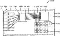
参照图1,在一个实施例中,印刷电路板(PCB)100包括在绝缘基底105上的外焊盘115和在绝缘基底105内的旁路焊盘(bypass pad)120。外焊盘115用来将外部装置(例如数码相机、电子游戏机、蜂窝式电话或个人计算机)与安装在PCB 100上的半导体芯片相互连接,使得信号可在它们之间进行通信。PCB 100可在多种应用中使用,上述多种应用包括如图25所示的固态盘(SSD)、存储卡或系统级封装(SIP,System-in-Package)半导体装置等。电子装置可包括两种或更多种类型的半导体芯片,例如存储芯片和逻辑芯片。为了在半导体芯片被封装和/或电子装置被制造之后保证半导体芯片的可靠性,执行测试工艺。此外,有需要测试工艺的各种其他场合,例如,在开发电子装置的过程中。Referring to FIG. 1 , in one embodiment, a printed circuit board (PCB) 100 includes
为了有助于测试,使电子装置(例如,SIP)包括除了外焊盘115之外的旁路焊盘120是有帮助的,其中旁路焊盘120也可被称为测试焊盘。旁路焊盘120可以是有用的,尤其是当包含半导体芯片的电子装置(例如存储卡)非常小的时候。旁路焊盘120可被用于测试电子装置内部的存储芯片。因此,在正常的制造工艺中或当触发特定的测试步骤时,即使在控制器芯片不正常工作的情况下,也可对存储芯片进行测试。To facilitate testing, it is helpful for an electronic device (eg, a SIP) to include
如果旁路焊盘120从PCB 100的绝缘基底105的表面暴露在外,会需要绝缘带来保护暴露的旁路焊盘免受外部环境影响。然而,在正常使用中,绝缘带会被剥落或损坏,从而使全部或部分旁路焊盘120暴露于外部环境。当旁路焊盘120被暴露到外部环境时,会出现旁路焊盘120中的相应的旁路焊盘之间的短路和电子装置的故障。If the
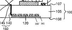
图2是根据处理该问题的本发明构思的一个实施例的图1中所示的PCB的剖视图。FIG. 2 is a cross-sectional view of the PCB shown in FIG. 1 according to one embodiment of the inventive concept dealing with this problem.
参照图2,根据本发明构思的一些实施例的PCB 100包括具有第一表面107和与第一表面107相对的第二表面108的绝缘基底105。绝缘基底105可包括具有单一介电层或多个介电层的刚性或柔性基底。PCB 100还包括设置为邻近第二表面108的外焊盘115和设置在第一表面107与第二表面108之间的旁路焊盘120。在一个实施例中,如所示的,旁路焊盘120可邻近第二表面108,并且与第一表面107相比,可更接近第二表面108。因此,旁路焊盘可整个包含在绝缘基底105中。此外,旁路焊盘120和外焊盘115可设置为邻近PCB 100的绝缘基底105的同侧。Referring to FIG. 2 , a
外焊盘115可形成在第二表面108上或设置在形成在绝缘基底105中的凹槽中。结果,外焊盘115可从第二表面108暴露以结合到外部装置,例如,包括膝上计算机、个人数字助理(PDA)和电子游戏机的各种电子装置。The
在一个实施例中,例如,旁路焊盘120可形成在邻近PCB 100的绝缘基底105的第二表面108的芯绝缘体(core insulator)(在图2中未示出,但在图20A至图20C中以标号106示出)的第二表面上。PCB 100可在芯绝缘体上具有阻焊剂层(在图2中未示出,但在图20C中以标号124示出)。如将在下面参照图20C描述的,阻焊剂层可包括分别暴露旁路焊盘120中对应的旁路焊盘120的开口。In one embodiment, for example, the
外焊盘115可通过一个或多个第一通孔塞130连接到PCB 100的绝缘基底105的上表面(即,第一表面107)上的一个或多个第一终端焊盘125。此外,可使用各种其他电连接方法来使外焊盘115和一个或多个第一终端焊盘125相互连接。The
旁路焊盘120也可利用一个或多个第二通孔塞140和/或引线图案145(共同称为“电路图案150”)连接到第一表面107上的一个或多个第二终端焊盘135。The
旁路焊盘可通过例如绝缘基底105来从外部环境密封。绝缘基底105可包括光致抗蚀剂材料。具体地说,制造PCB 100的材料可基本包围旁路焊盘120。旁路焊盘120可设置在PCB 100的区域中,在该区域中旁路焊盘的所有表面都被PCB 100包围。The bypass pads may be sealed from the external environment by, for example, the insulating
因此,根据本发明构思的一些实施例,保护旁路焊盘120免受外部环境影响,使得PCB 100和包括PCB 100的电子装置的可靠性提高。即使当压力或外部冲击被不经意地施加到PCB 100或包括PCB 100的电子装置时,由于旁路焊盘120设置在绝缘基底105内或PCB 100内,所以旁路焊盘120也能被安全地保护。应注意的是,本发明构思既应用于易失性电子装置,也应用于非易失性电子装置。换言之,上面讨论的半导体芯片可被提供作为例如DRAM、PRAM、MRAM、非易失性存储器等或它们的组合。Therefore, according to some embodiments of the inventive concept, the
图3是根据本发明构思的另一实施例的PCB的剖视图。FIG. 3 is a cross-sectional view of a PCB according to another embodiment of the inventive concept.
参照图3,有时在电子装置制造工艺的过程中或在制造完成之后,会需要对PCB 100上的半导体芯片进行测试。在这种情况下,绝缘基底105的第二表面108可被部分地去除,使得一个或多个旁路焊盘120从PCB 100暴露。然后可利用暴露的旁路焊盘120对半导体芯片进行测试。可利用包括干蚀刻、湿蚀刻和/或平面化第二表面108的若干方法来暴露旁路焊盘120。可利用回蚀(etch back)工艺或化学机械抛光(CMP)工艺来执行平面化。Referring to FIG. 3, it is sometimes necessary to test the semiconductor chip on the
在测试工序之后,如果需要,可通过例如沉积光致抗蚀剂的层来恢复第二表面108的被去除的部分。After the test procedure, the removed portion of the
可根据PCB 100的期望的应用来确定旁路焊盘120和外焊盘115的数量。如所示,旁路焊盘120可以以矩阵形式排列。The number of
图4和图5分别是根据本发明构思的一些实施例的电子装置的俯视图和剖视图。4 and 5 are top and cross-sectional views, respectively, of an electronic device according to some embodiments of the inventive concepts.
参照图4和图5,电子装置200包括设置在绝缘基底105的第一表面107上的半导体芯片205。电子装置200可以是存储卡等,并且半导体芯片205可以是例如存储芯片或逻辑芯片(或控制器芯片)。半导体芯片205可以电连接到外焊盘115和/或旁路焊盘120。外焊盘115可用于在半导体芯片205和电子装置200外部的组件(例如,诸如数码相机等的外部装置)之间传输信号。旁路焊盘120可被用于半导体芯片205的常规测试和/或失效分析。Referring to FIGS. 4 and 5 , the
半导体芯片205可包括一组或多组芯片焊盘210和240。芯片焊盘210和240的组可分别利用诸如键合引线215和245的连接装置结合到第一终端焊盘125和第二终端焊盘135。键合引线215和245的末端可连接到芯片焊盘210和240以及第一终端焊盘125和第二终端焊盘135。芯片焊盘210和240的组可利用导电凸点或导电通孔(through via)结合到第一终端焊盘125和第二终端焊盘135。
在一个实施例中,一个或多个无源器件(例如,电容器、电阻器或感应器)形成在绝缘基底105的第一表面上。In one embodiment, one or more passive devices (eg, capacitors, resistors, or inductors) are formed on the first surface of the insulating
在一些实施例中,可形成由诸如环氧模塑料(EMC,epoxy moldingcompound)的材料形成的密封剂225以覆盖半导体芯片205。在图4中,密封剂225被示出为虚线。密封剂225也可由陶瓷材料形成,或者密封剂225可以是由诸如金属的材料形成的壳(casing)。In some embodiments, an
电子装置200可利用外焊盘115电连接到例如各种电子装置的外部装置。在正常应用中,旁路焊盘120可被安全地保护在绝缘基底105中。然而,如上面所讨论的,当需要测试电子装置200或半导体芯片205时,可将旁路焊盘120暴露以进行测试。The
图6和图7分别是根据本发明构思的一个实施例的电子装置的俯视图和剖视图。图6和图7中示出的实施例包括与上面参照图4和图5描述的特征相似的特征。因此,为了简洁起见,将省略冗余的描述。6 and 7 are top and cross-sectional views, respectively, of an electronic device according to an embodiment of the inventive concept. The embodiment shown in FIGS. 6 and 7 includes similar features to those described above with reference to FIGS. 4 and 5 . Therefore, redundant descriptions will be omitted for brevity.
参照图6和图7,电子装置300可包括堆叠在绝缘基底105的第一表面107上的存储芯片305和逻辑芯片335。存储芯片305可包括各种类型的存储装置,例如闪存、DRAM、SRAM、PRAM(相位改变RAM)和RRAM(电阻RAM)。可设置逻辑芯片335来控制存储芯片305,并且存储芯片305可响应来自逻辑芯片335的命令来传输数据。电子装置300可以是例如MMC(多媒体卡)、SD(安全数字卡)、微型MMC、微型SD等。Referring to FIGS. 6 and 7 , the
外焊盘115可电连接到逻辑芯片335,使得逻辑芯片335可与外部装置交换信号。The
还可在PCB 100的绝缘基底105的第一表面107上设置一个或多个无源器件320。无源器件320可电连接到旁路焊盘120,并且无源器件320包括电容器、电阻器和/或感应器。One or more
在一些实施例中,可形成由诸如环氧模塑料(EMC)的材料形成的密封剂325以覆盖半导体芯片305和逻辑芯片335。In some embodiments,
图8是根据本发明构思的另一实施例的电子装置的俯视图。FIG. 8 is a top view of an electronic device according to another embodiment of the inventive concept.
参照图8,电子装置300a包括堆叠在PCB 100的绝缘基底105上的存储芯片305a和逻辑芯片335。存储芯片305a的芯片焊盘310a与逻辑芯片335的芯片焊盘340和350可被构造在不同的方向。具体地说,存储芯片305a的芯片焊盘310a可以沿纵向方向布置,而逻辑芯片335的芯片焊盘340和350可以沿横向方向布置。存储芯片305a的芯片焊盘310a可连接到可与第二终端焊盘135结合的第三终端焊盘135a。这样,逻辑芯片335和存储芯片305a中的每个芯片的键合引线315a、345、355被设置在不同的方向,使得可避免键合引线之间的电短路。8, the
图9是根据本发明构思的又一个实施例的电子装置的剖视图。FIG. 9 is a cross-sectional view of an electronic device according to still another embodiment of the inventive concept.
参照图9,电子装置300b包括设置在存储芯片305和逻辑芯片335之间的一个或多个附加存储芯片305b。在这种情况下,逻辑芯片335可控制存储芯片305和附加存储芯片305b。可堆叠附加存储芯片305b以暴露存储芯片305的芯片焊盘310。因此,附加存储芯片305b的芯片焊盘310b可通过诸如键合引线315b的连接装置连接到存储芯片305的芯片焊盘310。逻辑芯片335、存储芯片305和附加存储芯片305b可通过第二终端焊盘135和电路图案150电连接到旁路焊盘120。Referring to FIG. 9 , the
图10是根据本发明构思的一些实施例的电子装置的剖视图。FIG. 10 is a cross-sectional view of an electronic device according to some embodiments of the inventive concepts.
参照图10,电子装置300c包括设置在存储芯片305和逻辑芯片335之间的一个或多个附加存储芯片305b。因此,附加存储芯片305b的一个或多个附加芯片焊盘310b可通过键合引线315c直接电连接到第二终端焊盘135,而不是通过存储芯片焊盘310电连接到第二终端焊盘135。Referring to FIG. 10 , the
图11和图12分别是根据本发明构思的一些实施例的电子装置的俯视图和剖视图。11 and 12 are top and cross-sectional views, respectively, of an electronic device according to some embodiments of the inventive concepts.
参照图11和图12,电子装置300d包括存储芯片305d和逻辑芯片335d,存储芯片305d和逻辑芯片335d都直接设置在绝缘基底105上,而不是像其它实施例中那样是堆叠的。逻辑芯片335d可被构造为在第一终端焊盘125和第二终端焊盘135之间。因此,键合引线345、355可形成在逻辑芯片335d的相对侧。这样,可避免键合引线345和355之间的短路。11 and 12, the
图13和图14是图11和图12所示的实施例的可选实施例的剖视图。13 and 14 are cross-sectional views of alternative embodiments to the embodiment shown in FIGS. 11 and 12 .
参照图13和图14,电子装置300e可包括直接设置在绝缘基底105上的存储芯片305d和逻辑芯片335d以及设置在存储芯片305d上的附加存储芯片305e。逻辑芯片335d可控制存储芯片305d和附加存储芯片305e。附加存储芯片305e可被设置为暴露存储芯片305d的芯片焊盘310。因此,可通过键合引线315e将芯片焊盘310e连接到存储芯片305d的芯片焊盘310(见图13)。可选地,可使用键合引线315f将芯片焊盘310e直接连接到第二终端焊盘135。此外,逻辑芯片335d、存储芯片305d和附加存储芯片305e可通过第二终端焊盘135电连接到旁路焊盘120。13 and 14, the
图15至图17是图13中所示的电子装置的旁路焊盘部分的剖视图。15 to 17 are cross-sectional views of a bypass pad portion of the electronic device shown in FIG. 13 .
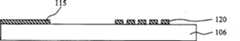
参照图15和图16,旁路焊盘120可被绝缘材料层160保护,从而旁路焊盘120不暴露在外。绝缘材料层160可直接设置在旁路焊盘120上。绝缘材料层160可包含例如环氧树脂、通孔填充材料或各向异性导电膜(ACF)的与阻焊剂材料相反的材料。如将要参照图21进一步描述的,当绝缘材料层160由ACF形成,并且需要测试电子装置中的存储芯片时,可放置测试尖端(testingtip)以在ACF上施加压力,使ACF电连接到旁路焊盘120。由于不需要额外的工艺来使旁路焊盘120暴露,所以可在相当程度上降低制造成本并缩短制造时间。Referring to FIGS. 15 and 16 , the
另一方面,如果旁路焊盘120由铜形成,则绝缘材料层160可直接形成在铜的裸露表面上。因此,不需要作为种子层的镍-金镀。结果,可降低在材料成本方面的制造成本并缩短工艺时间。On the other hand, if the
此外,与现有技术中的使用绝缘带覆盖旁路焊盘的方法相比,绝缘材料层160更不容易剥落,且不容易将旁路焊盘120暴露到外部环境。In addition, compared with the method of covering the bypass pads with an insulating tape in the prior art, the insulating
绝缘材料层160可包含具有相对于阻焊剂层的蚀刻选择性的介电材料,所述阻焊剂层邻近接近绝缘材料层160的PCB 100的第二表面108。因此,通过诸如蚀刻和抛光的化学和/或机械方法,绝缘材料层160可比光阻焊剂(PSR)材料更容易地去除。在PSR的情况下,由于PSR是硬质材料,所以对PSR的蚀刻需要诸如硝酸或硫酸的强化学蚀刻剂。因此,强化学蚀刻剂会蚀刻其它绝缘材料,导致短路。通过使用更容易去除的绝缘材料层160,可减少诸如短路的这些问题。The layer of insulating
如图16所示,绝缘材料层160可如期望地只设置在旁路焊盘120的总数的一部分上。换言之,绝缘基底105包括一个或多个暴露旁路焊盘120的一部分的开口159。所述一个或多个开口159填充有相对于绝缘基底105(例如,形成绝缘基底105的阻焊剂层)具有蚀刻选择性的绝缘材料层160。As shown in FIG. 16 , the insulating
如图17所示,附加阻焊剂层可形成在PCB 100的第二表面108上以覆盖阻焊剂层和绝缘材料层160。As shown in FIG. 17 , an additional layer of solder resist may be formed on the
继续参照图17,绝缘材料层160可设置在PCB 100的内部(即,在PCB 100的第二表面108下面)和/或在形成在PCB 100的第二表面108上的附加阻焊剂层123下面。在这种情况下,为了暴露旁路焊盘120,可顺序地应用机械抛光和化学蚀刻。With continued reference to FIG. 17 , a layer of insulating
图18是示出覆盖PCB的表面的旁路焊盘区的绝缘材料层的俯视图。图19是图18中所示的电子装置的旁路焊盘部分的剖视图。18 is a top view showing a layer of insulating material covering a bypass pad region of the surface of the PCB. FIG. 19 is a cross-sectional view of a bypass pad portion of the electronic device shown in FIG. 18 .
在图17中,绝缘材料层160形成在单独的旁路焊盘120上,而不是形成在旁路焊盘120之间的区域上。然而,如图18和19所示,单个绝缘材料层160’可设置在多个旁路焊盘120(包括旁路焊盘120之间的区域)上。换言之,在绝缘基底105的一部分中可以有上覆在多个旁路焊盘120上的单个开口161,而不是只在单独的旁路焊盘120上具有开口161。并且单个绝缘材料层160’可设置在单个开口161中以将单个绝缘材料层160’设置在多个旁路焊盘120上。虽然SR层没有独立地在图19中示出,但是绝缘基底105的其他部分在未形成单个绝缘材料层160’的区域中包括SR层。单个绝缘材料层160’可由相对于SR层具有蚀刻选择性的介电材料形成。可以看出SR层包括设置在多个旁路焊盘120上的单个开口161。换言之,SR层可包括暴露多个旁路焊盘120的单个开口161。In FIG. 17 , the insulating
在一个实施例中,例如在图17中,单个绝缘材料层160’可由与绝缘材料层160相似的材料形成。In one embodiment, such as in FIG. 17, a single layer of insulating material 160' may be formed of a similar material as
图20A至图20C是示出根据本发明构思的一些实施例的制造包括旁路焊盘的PCB的方法的剖视图。20A to 20C are cross-sectional views illustrating a method of manufacturing a PCB including a bypass pad according to some embodiments of the inventive concepts.
参照图20A,制造PCB的方法包括提供芯绝缘体106。芯绝缘体106可包含但不限于双马来酰亚胺三嗪树脂(BT树脂)材料。接着,在芯绝缘体106上形成导电图案。导电图案包括外焊盘115和旁路焊盘120。形成导电图案的步骤可包括形成导电材料层并随后使导电材料层图案化(例如,利用光刻工艺)以形成外焊盘115和旁路焊盘120。Referring to FIG. 20A , the method of manufacturing a PCB includes providing a
参照图20B,介电层122形成在芯绝缘体106的包括外焊盘115和旁路焊盘120的基本整个表面上。介电层122可以是阻焊剂,更具体地说,可以是光阻焊剂(PSR)。Referring to FIG. 20B , a
参照图20C,介电层122的一部分被去除以形成阻焊剂层124。去除介电层122的一部分的步骤可包括光刻工艺。外焊盘115被阻焊剂层124暴露。旁路焊盘120可不被阻焊剂层124暴露(或可被阻焊剂层124覆盖)。可选地,旁路焊盘120中的一些可被阻焊剂层124暴露,而旁路焊盘120中的另一些可不被阻焊剂层124暴露(或可被阻焊剂层124覆盖)。虽然为了简洁而没有示出,但是其它传统的PCB材料可形成在芯绝缘体106上。例如,在芯绝缘体106的与阻焊剂层124相对的另一侧上形成另一个光致抗蚀剂层。Referring to FIG. 20C , a portion of the
在一个实施例中,由包括图15至图17的附图示出的绝缘基底105可具有与图20C中所示的结构相似的结构。换言之,例如,绝缘基底105可包括芯绝缘体,芯绝缘体上形成有旁路焊盘120,同时阻焊剂层覆盖旁路焊盘和芯绝缘体,如图20C所示。然而,本发明不限于该具体结构,并且本发明可以应用于在本发明的精神和范围内的任何其他适合的PCB结构。In one embodiment, the insulating
此外,关于特定附图或实施例讨论的一些或全部特征也可被应用到其他实施例或附图。Furthermore, some or all features discussed with respect to a particular figure or embodiment may also be applicable to other embodiments or figures.
图21是根据上面关于图15至图16讨论的本发明构思的一些实施例的包括具有ACF的旁路焊盘的PCB的剖视图。21 is a cross-sectional view of a PCB including a bypass pad with an ACF according to some embodiments of the inventive concepts discussed above with respect to FIGS. 15 to 16 .
参照图21,根据本发明的一个实施例,PCB 101包括芯绝缘体106、外焊盘115、旁路焊盘120、阻焊剂层124。外焊盘115从阻焊剂层124暴露。旁路焊盘120也从阻焊剂层124暴露,然而在这种情况下,各向异性导电膜(ACF)126覆盖旁路焊盘120。利用ACF126,测试探针2010可电接触旁路焊盘120以测试存储芯片。Referring to FIG. 21 , according to one embodiment of the present invention, a
图22是根据本发明构思的一些实施例的测试电子装置的方法的视图。FIG. 22 is a view of a method of testing an electronic device according to some embodiments of the inventive concepts.
参照图22,测试电子装置的方法包括提供PCB(步骤2110)。PCB包括用于与外部装置结合的多个外焊盘和用于测试电路的多个旁路焊盘。外焊盘从PCB的外表面暴露。然而,一个或多个旁路焊盘不从PCB的外表面暴露。该方法还包括去除PCB的一部分以暴露多个旁路焊盘中的至少一个(步骤2120)。最后,该方法包括通过多个旁路焊盘中的所述至少一个来测试电路(步骤2130)。Referring to FIG. 22, the method of testing an electronic device includes providing a PCB (step 2110). The PCB includes a plurality of external pads for coupling with external devices and a plurality of bypass pads for testing circuits. The outer pads are exposed from the outer surface of the PCB. However, one or more bypass pads are not exposed from the outer surface of the PCB. The method also includes removing a portion of the PCB to expose at least one of the plurality of bypass pads (step 2120). Finally, the method includes testing the circuit via the at least one of the plurality of bypass pads (step 2130).
图23是使用根据本发明构思的实施例的电子装置的系统的视图。FIG. 23 is a view of a system using an electronic device according to an embodiment of the inventive concept.
参照图23,系统400包括插槽(socket)420、包括参照上述实施例讨论的PCB的电子装置410、卡界面控制器430和主机或外部装置440。插槽420可被提供为允许电子装置410插入并与电子装置410接触。电子装置410可以是例如存储卡。插槽420可连接到电子装置410的外焊盘115(例如,在图15中示出)。卡界面控制器430可通过插槽420控制与电子装置410的数据交换。卡界面控制器430还可用于在电子装置410中存储数据。主机440控制卡界面控制器430。Referring to FIG. 23 , a
图24是使用根据本发明构思的实施例的电子装置的另一系统的视图。FIG. 24 is a view of another system using an electronic device according to an embodiment of the inventive concept.
参照图24,例如,系统800可包括处理器810(例如,应用在个人计算机、游戏机、PDA等中的中央处理单元(CUP))、根据上述任意一个实施例制造的电子装置820、输入/输出装置830和总线840。输入/输出装置830可电连接到微处理器810和电子装置820(例如,通过总线840)。虽然未示出,但是可将控制器添加到系统800。Referring to FIG. 24, for example, a system 800 may include a processor 810 (for example, a central processing unit (CUP) applied in a personal computer, a game machine, a PDA, etc.), an electronic device 820 manufactured according to any of the above-mentioned embodiments, an input/ output device 830 and bus 840 . Input/output device 830 may be electrically connected to microprocessor 810 and electronics 820 (eg, via bus 840). Although not shown, a controller may be added to system 800 .
在一个实施例中,系统800可被设置为移动电话、MP3播放器、导航装置、固态盘(SSD)、家用电器等的一部分。In one embodiment, system 800 may be provided as part of a mobile phone, MP3 player, navigation device, solid state drive (SSD), home appliance, or the like.
图25示出了使用根据本发明构思的实施例的电子装置的固态盘(SSD)的照片。具体地说,图25示出了SSD的外壳的前侧和后侧以及放在外壳中的PCB的前侧和后侧。如所示,控制器和连接器设置在PCB的前侧而闪速存储器设置在PCB的两侧。然而,本发明的实施例不限于该特定结构,并且本发明的实施例可以以包含在本发明的精神和范围内的其他方式来实施。例如,连接器可设置在PCB的另一侧,并且连接器的位置可根据应用来设置。FIG. 25 shows a photograph of a solid state disk (SSD) using an electronic device according to an embodiment of the inventive concept. Specifically, FIG. 25 shows the front and rear sides of the housing of the SSD and the front and rear sides of the PCB placed in the housing. As shown, the controller and connectors are located on the front side of the PCB and the flash memory is located on both sides of the PCB. However, the embodiments of the present invention are not limited to this specific structure, and the embodiments of the present invention may be implemented in other ways included within the spirit and scope of the present invention. For example, the connector may be provided on the other side of the PCB, and the position of the connector may be set according to the application.
根据本发明构思的一些实施例,印刷电路板(PCB)包括:多个外焊盘,用于与外部装置连接;多个旁路焊盘,用于测试电路。外焊盘可从PCB的外表面暴露,一个或多个旁路焊盘可不从PCB的外表面暴露。旁路焊盘可整个包含在PCB中。此外,旁路焊盘和外焊盘可设置为邻近PCB的同一侧。According to some embodiments of the inventive concepts, a printed circuit board (PCB) includes: a plurality of external pads for connecting with external devices; and a plurality of bypass pads for testing circuits. The outer pads may be exposed from the outer surface of the PCB, and one or more bypass pads may not be exposed from the outer surface of the PCB. The bypass pad can be included entirely on the PCB. Additionally, bypass pads and outer pads can be located adjacent to the same side of the PCB.
根据本发明构思的其他实施例,印刷电路板(PCB)包括:芯绝缘体,具有顶表面和底表面;旁路焊盘,形成在芯绝缘体的底表面上,用于测试电路;外焊盘,形成在芯绝缘体的底表面上,用于与外部装置连接;阻焊剂(SR)层,暴露外焊盘并覆盖旁路焊盘中的至少一个。形成PCB的材料可基本包围旁路焊盘。旁路焊盘可设置在PCB的区域中,在该区域中旁路焊盘的所有表面都被PCB包围。SR层可包括分别暴露旁路焊盘中对应的旁路焊盘的开口。开口可由相对于阻焊剂层具有蚀刻选择性的介电材料填充。开口可由ACF填充。对于预定的蚀刻剂,介电材料可比阻焊剂层蚀刻得快。SR层可具有暴露旁路焊盘中的一部分的至少一个开口,所述至少一个开口可填充介电材料,并且所述开口的至少一个的其它部分可被阻焊剂覆盖。可选地,SR层可包括暴露多个旁路焊盘的单个开口,并且所述单个开口可由相对于SR层具有蚀刻选择性的介电材料填充,所述介电材料覆盖所述多个旁路焊盘。PCB还可包括另一阻焊剂(SR)层以覆盖具有开口的SR层和介电材料。According to other embodiments of the present inventive concept, a printed circuit board (PCB) includes: a core insulator having a top surface and a bottom surface; a bypass pad formed on the bottom surface of the core insulator for testing a circuit; an outer pad, Formed on the bottom surface of the core insulator for connection with external devices; a solder resist (SR) layer exposing the outer pads and covering at least one of the bypass pads. The material forming the PCB may substantially surround the bypass pad. The bypass pads may be arranged in regions of the PCB in which all surfaces of the bypass pads are surrounded by the PCB. The SR layer may include openings respectively exposing corresponding ones of the bypass pads. The opening may be filled with a dielectric material having etch selectivity with respect to the solder resist layer. The opening can be filled with ACF. The dielectric material may etch faster than the solder resist layer for a given etchant. The SR layer may have at least one opening exposing a portion of the bypass pad, the at least one opening may be filled with a dielectric material, and other portions of at least one of the openings may be covered with solder resist. Alternatively, the SR layer may include a single opening exposing a plurality of bypass pads, and the single opening may be filled with a dielectric material having etch selectivity with respect to the SR layer, the dielectric material covering the plurality of bypass pads. road pad. The PCB may also include another layer of solder resist (SR) to cover the SR layer with openings and the dielectric material.
根据本发明构思的又一个实施例,一种装置包括PCB和上覆在PCB上的半导体芯片。PCB可包括:芯绝缘体,具有顶表面和底表面;旁路焊盘,形成在芯绝缘体的底表面上,用于测试电路;外焊盘,形成在芯绝缘体的底表面上,用于与外部装置连接;阻焊剂层,暴露外焊盘并覆盖旁路焊盘中的至少一个。半导体芯片可包括:存储芯片,上覆在PCB上;控制器芯片,上覆在PCB上。所述装置可以是存储装置。存储装置可以是SSD或存储卡。According to still another embodiment of the inventive concept, an apparatus includes a PCB and a semiconductor chip overlying the PCB. The PCB may include: a core insulator having top and bottom surfaces; bypass pads formed on the bottom surface of the core insulator for testing circuits; outer pads formed on the bottom surface of the core insulator for communicating with external A device connection; a layer of solder resist exposing the outer pads and covering at least one of the bypass pads. The semiconductor chip may include: a memory chip overlying the PCB; and a controller chip overlying the PCB. The device may be a storage device. The storage device may be an SSD or a memory card.
根据本发明构思的再一个实施例,一种系统包括:PCB基底;阻焊剂;半导体存储芯片;控制器和CPU中的至少一个。PCB基底包括:芯绝缘体,具有顶表面和底表面;旁路焊盘,形成在芯绝缘体的底表面上,用于测试电路;外焊盘,形成在芯绝缘体的底表面上,用于与外部装置连接。阻焊剂暴露外焊盘并覆盖旁路焊盘中的至少一个。According to still another embodiment of the inventive concept, a system includes: a PCB substrate; a solder resist; a semiconductor memory chip; at least one of a controller and a CPU. The PCB substrate includes: a core insulator having a top surface and a bottom surface; a bypass pad formed on the bottom surface of the core insulator for testing a circuit; an outer pad formed on the bottom surface of the core insulator for communicating with an external device connection. The solder resist exposes the outer pads and covers at least one of the bypass pads.
根据本发明构思的另一实施例,一种方法包括以下步骤:提供印刷电路板(PCB),PCB包括多个用于与外部装置连接的外焊盘和多个用于测试电路的旁路焊盘;去除PCB的一部分以暴露所述多个旁路焊盘中的至少一个;通过所述多个旁路焊盘中的所述至少一个来测试电路。外焊盘暴露于PCB的外表面,旁路焊盘的一个或多个未暴露于PCB的外表面。电路可以是存储器。According to another embodiment of the present inventive concept, a method includes the steps of: providing a printed circuit board (PCB) including a plurality of external pads for connection to external devices and a plurality of bypass pads for testing circuits removing a portion of the PCB to expose at least one of the plurality of bypass pads; testing a circuit through the at least one of the plurality of bypass pads. The outer pads are exposed on the outer surface of the PCB, and one or more of the bypass pads are not exposed on the outer surface of the PCB. A circuit may be a memory.
PCB可包括阻焊剂层,并且去除PCB的一部分的步骤可包括:去除阻焊剂层的一部分以形成至少一个开口,所述至少一个开口暴露多个旁路焊盘中的至少一个;在所述至少一个开口中形成各向异性导电膜(ACF)。测试电路的步骤可包括使测试探针接触ACF。The PCB may include a solder resist layer, and the step of removing a portion of the PCB may include: removing a portion of the solder resist layer to form at least one opening exposing at least one of the plurality of bypass pads; An anisotropic conductive film (ACF) is formed in one opening. The step of testing the circuit may include contacting a test probe to the ACF.
根据本发明构思的又一实施例,一种形成印刷电路板(PCB)的方法包括以下步骤:提供芯绝缘体;在芯绝缘体的表面上形成外焊盘和旁路焊盘;在芯绝缘体的所述表面上形成阻焊剂层。阻焊剂层暴露外焊盘并覆盖旁路焊盘中的至少一个。形成外焊盘和旁路焊盘的步骤可包括:在芯绝缘体的所述表面上形成导电材料层;将导电材料层图案化以形成外焊盘和旁路焊盘。形成阻焊剂层的步骤可包括:在芯绝缘体的所述表面、外焊盘和旁路焊盘上形成介电层;将介电层图案化以形成阻焊剂层。According to yet another embodiment of the present inventive concept, a method of forming a printed circuit board (PCB) includes the steps of: providing a core insulator; forming an outer pad and a bypass pad on a surface of the core insulator; A solder resist layer is formed on the surface. The solder resist layer exposes the outer pads and covers at least one of the bypass pads. The forming of the outer pad and the bypass pad may include: forming a conductive material layer on the surface of the core insulator; and patterning the conductive material layer to form the outer pad and the bypass pad. The forming of the solder resist layer may include: forming a dielectric layer on the surface of the core insulator, the outer pad and the bypass pad; and patterning the dielectric layer to form the solder resist layer.
参照整个说明书,“一个实施例”和“实施例”表示结合该实施例描述的特定的特征、结构或特性包含在本发明的至少一个实施例中。因此,在整个本说明书中的各个位置出现的短语“在一个实施例中”、“在一些实施例中”和“在实施例中”不需要全部指示同一实施例。此外,在一个或多个实施例中,特定的特征、结构或特性可以以任何合适的方式结合。References throughout this specification to "one embodiment" and "an embodiment" mean that a particular feature, structure, or characteristic described in connection with the embodiment is included in at least one embodiment of the invention. Thus, appearances of the phrases "in one embodiment," "in some embodiments," and "in an embodiment" in various places throughout this specification are not necessarily all referring to the same embodiment. Furthermore, the particular features, structures or characteristics may be combined in any suitable manner in one or more embodiments.
各种操作将被描述为按照对理解本发明最有帮助的方式执行的多个不连续的步骤。然而,描述步骤的顺序不意味着这些操作是依赖顺序的,也不意味着这些步骤必须按照呈现步骤的顺序来执行。Various operations will be described as multiple discrete steps performed in a manner that is most helpful in understanding the invention. However, the order in which the steps are described does not imply that these operations are order dependent, nor that the steps must be performed in the order in which the steps are presented.
虽然已经参照本发明构思的示例性实施例具体地示出并描述了本发明构思,但是本领域普通技术人员应该理解,在不脱离如权利要求限定的本发明构思的精神和范围的情况下,可进行各种形式和细节上的改变。While the inventive concept has been particularly shown and described with reference to exemplary embodiments thereof, it should be understood by those of ordinary skill in the art that, without departing from the spirit and scope of the inventive concept as defined by the claims, Various changes in form and detail may be made.
Claims (38)
Applications Claiming Priority (5)
| Application Number | Priority Date | Filing Date | Title |
|---|---|---|---|
| KR1020070129057 | 2007-12-12 | ||
| KR20070129057 | 2007-12-12 | ||
| KR10-2007-0129057 | 2007-12-12 | ||
| US12/204,735 | 2008-09-04 | ||
| US12/204,735US7872483B2 (en) | 2007-12-12 | 2008-09-04 | Circuit board having bypass pad |
Publications (2)
| Publication Number | Publication Date |
|---|---|
| CN101459155Atrue CN101459155A (en) | 2009-06-17 |
| CN101459155B CN101459155B (en) | 2014-11-05 |
Family
ID=40752346
Family Applications (1)
| Application Number | Title | Priority Date | Filing Date |
|---|---|---|---|
| CN200810179478.XAActiveCN101459155B (en) | 2007-12-12 | 2008-11-28 | method, divece and system for forming printed circuit board, printed circuit board, and method for detecting circuit |
Country Status (5)
| Country | Link |
|---|---|
| US (8) | US7872483B2 (en) |
| KR (1) | KR101516656B1 (en) |
| CN (1) | CN101459155B (en) |
| DE (1) | DE102008050875A1 (en) |
| TW (1) | TWI419618B (en) |
Cited By (10)
| Publication number | Priority date | Publication date | Assignee | Title |
|---|---|---|---|---|
| CN102467977A (en)* | 2010-11-01 | 2012-05-23 | 中芯国际集成电路制造(上海)有限公司 | Chip fixing pedestal and chip fixed-connection mode |
| CN102480852A (en)* | 2010-11-22 | 2012-05-30 | 富葵精密组件(深圳)有限公司 | Method for manufacturing circuit board |
| CN105517337A (en)* | 2015-11-25 | 2016-04-20 | 武汉光迅科技股份有限公司 | High-reliability flexible plate and assembling system thereof |
| CN106304627A (en)* | 2015-05-13 | 2017-01-04 | 上海和辉光电有限公司 | A kind of test pad structure and preparation method thereof |
| CN107093593A (en)* | 2017-03-14 | 2017-08-25 | 深圳市江波龙电子有限公司 | One kind encapsulation chip and method for packing |
| CN109564254A (en)* | 2016-08-01 | 2019-04-02 | 恩德斯+豪斯流量技术股份有限公司 | circuit board with contact structure |
| CN110870390A (en)* | 2018-01-30 | 2020-03-06 | 株式会社Lg化学 | Method for producing a printed circuit board with test points and printed circuit board produced thereby |
| CN110996556A (en)* | 2020-01-07 | 2020-04-10 | 电子科技大学 | Welding method of multilayer interconnected FPC |
| CN113466657A (en)* | 2021-06-02 | 2021-10-01 | 长江存储科技有限责任公司 | Circuit board for chip testing, chip testing system and method |
| CN114863960A (en)* | 2021-01-20 | 2022-08-05 | 铠侠股份有限公司 | memory system |
Families Citing this family (40)
| Publication number | Priority date | Publication date | Assignee | Title |
|---|---|---|---|---|
| US7778057B2 (en)* | 2007-02-26 | 2010-08-17 | Sandisk Corporation | PCB circuit modification from multiple to individual chip enable signals |
| US7709278B2 (en)* | 2007-02-26 | 2010-05-04 | Sandisk Corporation | Method of making PCB circuit modification from multiple to individual chip enable signals |
| US7872483B2 (en) | 2007-12-12 | 2011-01-18 | Samsung Electronics Co., Ltd. | Circuit board having bypass pad |
| KR101097247B1 (en)* | 2009-10-26 | 2011-12-21 | 삼성에스디아이 주식회사 | Electronic circuit module and its manufacturing method |
| KR20110074135A (en)* | 2009-12-24 | 2011-06-30 | 삼성전자주식회사 | System-in-package with embedded circuit board |
| KR101085752B1 (en)* | 2010-05-10 | 2011-11-21 | 삼성전기주식회사 | Test method of circuit board and components mounted on the circuit board |
| USD637192S1 (en) | 2010-10-18 | 2011-05-03 | Apple Inc. | Electronic device |
| USD637193S1 (en)* | 2010-11-19 | 2011-05-03 | Apple Inc. | Electronic device |
| JP2013025540A (en)* | 2011-07-20 | 2013-02-04 | Toshiba Corp | Semiconductor storage device |
| US9121900B2 (en)* | 2011-12-02 | 2015-09-01 | Sandisk Technologies Inc. | Systems and methods for sensing signals communicated with a host device or on an interface of plug-in card when there is lack of access to sensing points |
| US9635794B2 (en)* | 2012-02-20 | 2017-04-25 | Trw Automotive U.S. Llc | Method and apparatus for attachment of integrated circuits |
| US9117790B2 (en)* | 2012-06-25 | 2015-08-25 | Marvell World Trade Ltd. | Methods and arrangements relating to semiconductor packages including multi-memory dies |
| USD709894S1 (en)* | 2012-09-22 | 2014-07-29 | Apple Inc. | Electronic device |
| US20140233195A1 (en)* | 2013-02-21 | 2014-08-21 | Kabushiki Kaisha Toshiba | Semiconductor device |
| USD758372S1 (en)* | 2013-03-13 | 2016-06-07 | Nagrastar Llc | Smart card interface |
| US9888283B2 (en) | 2013-03-13 | 2018-02-06 | Nagrastar Llc | Systems and methods for performing transport I/O |
| JP6402962B2 (en)* | 2013-07-17 | 2018-10-10 | パナソニックIpマネジメント株式会社 | High frequency module |
| KR102174069B1 (en)* | 2014-03-03 | 2020-11-05 | 삼성디스플레이 주식회사 | Printed circuit board and method of manufacturing a printed circuit board |
| USD864968S1 (en) | 2015-04-30 | 2019-10-29 | Echostar Technologies L.L.C. | Smart card interface |
| TWI536179B (en)* | 2015-07-02 | 2016-06-01 | 緯創資通股份有限公司 | Connecting circuitry and computing system haveing the same |
| KR102434435B1 (en) | 2015-10-26 | 2022-08-19 | 삼성전자주식회사 | Printed circuit board and semiconductor package having the same |
| KR102192569B1 (en)* | 2015-11-06 | 2020-12-17 | 삼성전자주식회사 | Electronic component package and manufactruing method of the same |
| US10041989B2 (en)* | 2016-03-09 | 2018-08-07 | Panasonic Liquid Crystal Display Co., Ltd. | Circuit board with inspection terminals |
| US9807872B2 (en)* | 2016-03-09 | 2017-10-31 | Panasonic Liquid Crystal Display Co., Ltd. | Circuit board and display device |
| US10034407B2 (en)* | 2016-07-22 | 2018-07-24 | Intel Corporation | Storage sled for a data center |
| DE102016114143A1 (en)* | 2016-08-01 | 2018-02-01 | Endress+Hauser Flowtec Ag | Test system for checking electronic connections of components with a printed circuit board and printed circuit board |
| TWD190983S (en)* | 2017-02-17 | 2018-06-11 | 三星電子股份有限公司 | Ssd storage device |
| CN108196182B (en)* | 2017-12-30 | 2020-04-21 | 大族激光科技产业集团股份有限公司 | Reference network selection method and device for flying probe test |
| USD869470S1 (en)* | 2018-04-09 | 2019-12-10 | Samsung Electronics Co., Ltd. | SSD storage device |
| USD869469S1 (en)* | 2018-04-09 | 2019-12-10 | Samsung Electronics Co., Ltd. | SSD storage device |
| TWI686924B (en)* | 2018-10-18 | 2020-03-01 | 普誠科技股份有限公司 | Integrated circuit and test method |
| CN109801671B (en)* | 2018-12-19 | 2021-02-12 | 珠海妙存科技有限公司 | Memory testing device and method compatible with eMMC protocol and SD protocol |
| CN111370054B (en)* | 2018-12-26 | 2024-07-05 | 华为技术有限公司 | Test system of memory card |
| US11166363B2 (en) | 2019-01-11 | 2021-11-02 | Tactotek Oy | Electrical node, method for manufacturing electrical node and multilayer structure comprising electrical node |
| US11637045B2 (en)* | 2019-01-29 | 2023-04-25 | Intel Corporation | Anisotropic conductive film (ACF) for use in testing semiconductor packages |
| TWI758675B (en)* | 2019-12-31 | 2022-03-21 | 新唐科技股份有限公司 | Microcontroller circuit and printed circuit board |
| KR20220141845A (en)* | 2020-02-28 | 2022-10-20 | 키오시아 가부시키가이샤 | semiconductor memory device |
| US20240038953A1 (en)* | 2020-12-08 | 2024-02-01 | Kyocera Corporation | Display device |
| CN214708142U (en)* | 2021-01-14 | 2021-11-12 | 株式会社和冠 | Control circuit board |
| JP2023031558A (en)* | 2021-08-25 | 2023-03-09 | キオクシア株式会社 | semiconductor storage device |
Family Cites Families (15)
| Publication number | Priority date | Publication date | Assignee | Title |
|---|---|---|---|---|
| US5630947A (en)* | 1994-12-28 | 1997-05-20 | Shi; Shei-Kung | Method of making a multichip module comprising at least one thin film probe |
| JPH10335035A (en) | 1997-05-30 | 1998-12-18 | Ando Electric Co Ltd | Measuring mechanism for bga-ic |
| JP3815936B2 (en)* | 2000-01-25 | 2006-08-30 | 株式会社ルネサステクノロジ | IC card |
| US6404649B1 (en)* | 2000-03-03 | 2002-06-11 | Advanced Micro Devices, Inc. | Printed circuit board assembly with improved bypass decoupling for BGA packages |
| US6858925B2 (en)* | 2001-04-02 | 2005-02-22 | Renesas Technology Corp. | Semiconductor device and a method of manufacturing the same |
| JP3595283B2 (en)* | 2001-06-27 | 2004-12-02 | 日本特殊陶業株式会社 | Wiring board and method of manufacturing the same |
| US20050013106A1 (en)* | 2003-07-17 | 2005-01-20 | Takiar Hem P. | Peripheral card with hidden test pins |
| KR101014576B1 (en)* | 2004-02-24 | 2011-02-16 | 이비덴 가부시키가이샤 | Semiconductor mounting board |
| US7626829B2 (en)* | 2004-10-27 | 2009-12-01 | Ibiden Co., Ltd. | Multilayer printed wiring board and manufacturing method of the multilayer printed wiring board |
| JP4843214B2 (en) | 2004-11-16 | 2011-12-21 | 株式会社東芝 | Module board and disk device |
| JP4185499B2 (en) | 2005-02-18 | 2008-11-26 | 富士通マイクロエレクトロニクス株式会社 | Semiconductor device |
| US7511359B2 (en)* | 2005-12-29 | 2009-03-31 | Intel Corporation | Dual die package with high-speed interconnect |
| US7359204B1 (en)* | 2006-02-15 | 2008-04-15 | Amkor Technology, Inc. | Multiple cover memory card |
| US8013332B2 (en) | 2006-10-20 | 2011-09-06 | Sandisk Technologies Inc. | Portable memory devices |
| US7872483B2 (en)* | 2007-12-12 | 2011-01-18 | Samsung Electronics Co., Ltd. | Circuit board having bypass pad |
- 2008
- 2008-09-04USUS12/204,735patent/US7872483B2/enactiveActive
- 2008-09-29DEDE102008050875Apatent/DE102008050875A1/enactivePending
- 2008-11-20KRKR1020080115799Apatent/KR101516656B1/enactiveActive
- 2008-11-28CNCN200810179478.XApatent/CN101459155B/enactiveActive
- 2008-12-11TWTW097148288Apatent/TWI419618B/enactive
- 2010
- 2010-07-16USUS12/837,649patent/US8248093B2/enactiveActive
- 2010-10-22USUS12/910,645patent/US8203355B2/enactiveActive
- 2012
- 2012-07-31USUS13/563,258patent/US8917107B2/enactiveActive
- 2013
- 2013-12-12USUS14/104,315patent/US9069036B2/enactiveActive
- 2015
- 2015-05-07USUS14/705,971patent/US9171644B2/enactiveActive
- 2015-05-22USUS14/719,321patent/US9449716B2/enactiveActive
- 2016
- 2016-09-12USUS15/262,304patent/US9627360B2/enactiveActive
Cited By (17)
| Publication number | Priority date | Publication date | Assignee | Title |
|---|---|---|---|---|
| CN102467977A (en)* | 2010-11-01 | 2012-05-23 | 中芯国际集成电路制造(上海)有限公司 | Chip fixing pedestal and chip fixed-connection mode |
| CN102480852A (en)* | 2010-11-22 | 2012-05-30 | 富葵精密组件(深圳)有限公司 | Method for manufacturing circuit board |
| CN102480852B (en)* | 2010-11-22 | 2014-02-05 | 富葵精密组件(深圳)有限公司 | Method for manufacturing circuit boards |
| CN106304627A (en)* | 2015-05-13 | 2017-01-04 | 上海和辉光电有限公司 | A kind of test pad structure and preparation method thereof |
| CN106304627B (en)* | 2015-05-13 | 2019-10-29 | 上海和辉光电有限公司 | A kind of test pad structure and preparation method thereof |
| CN105517337A (en)* | 2015-11-25 | 2016-04-20 | 武汉光迅科技股份有限公司 | High-reliability flexible plate and assembling system thereof |
| CN105517337B (en)* | 2015-11-25 | 2018-03-27 | 武汉光迅科技股份有限公司 | A kind of high reliability flexible board and its assembly system |
| CN109564254A (en)* | 2016-08-01 | 2019-04-02 | 恩德斯+豪斯流量技术股份有限公司 | circuit board with contact structure |
| US11002785B2 (en) | 2016-08-01 | 2021-05-11 | Endress+Hauser Flowtec Ag | Printed circuit board with contacting arrangement |
| WO2018166264A1 (en)* | 2017-03-14 | 2018-09-20 | 深圳市江波龙电子有限公司 | Packaged chip and packaging method |
| CN107093593B (en)* | 2017-03-14 | 2019-08-13 | 深圳市江波龙电子股份有限公司 | A kind of encapsulation chip and packaging method |
| CN107093593A (en)* | 2017-03-14 | 2017-08-25 | 深圳市江波龙电子有限公司 | One kind encapsulation chip and method for packing |
| CN110870390A (en)* | 2018-01-30 | 2020-03-06 | 株式会社Lg化学 | Method for producing a printed circuit board with test points and printed circuit board produced thereby |
| CN110996556A (en)* | 2020-01-07 | 2020-04-10 | 电子科技大学 | Welding method of multilayer interconnected FPC |
| CN114863960A (en)* | 2021-01-20 | 2022-08-05 | 铠侠股份有限公司 | memory system |
| CN113466657A (en)* | 2021-06-02 | 2021-10-01 | 长江存储科技有限责任公司 | Circuit board for chip testing, chip testing system and method |
| CN113466657B (en)* | 2021-06-02 | 2022-05-27 | 长江存储科技有限责任公司 | A circuit board, chip testing system and method for chip testing |
Also Published As
| Publication number | Publication date |
|---|---|
| US20110037491A1 (en) | 2011-02-17 |
| US20170018535A1 (en) | 2017-01-19 |
| US20150243371A1 (en) | 2015-08-27 |
| TWI419618B (en) | 2013-12-11 |
| US20100289157A1 (en) | 2010-11-18 |
| US8203355B2 (en) | 2012-06-19 |
| US9171644B2 (en) | 2015-10-27 |
| US20120292091A1 (en) | 2012-11-22 |
| DE102008050875A1 (en) | 2009-07-02 |
| TW200934311A (en) | 2009-08-01 |
| CN101459155B (en) | 2014-11-05 |
| KR20090063087A (en) | 2009-06-17 |
| US9069036B2 (en) | 2015-06-30 |
| US8917107B2 (en) | 2014-12-23 |
| US7872483B2 (en) | 2011-01-18 |
| US20150257255A1 (en) | 2015-09-10 |
| US20090153163A1 (en) | 2009-06-18 |
| US20140097865A1 (en) | 2014-04-10 |
| KR101516656B1 (en) | 2015-05-11 |
| US9449716B2 (en) | 2016-09-20 |
| US8248093B2 (en) | 2012-08-21 |
| US9627360B2 (en) | 2017-04-18 |
Similar Documents
| Publication | Publication Date | Title |
|---|---|---|
| TWI419618B (en) | Print circuit board and a method of forming the print circuit board,electronic device and a systen using the electronic device,and a method of testing an electric circuit | |
| US10325882B2 (en) | Method of manufacturing semiconductor package | |
| US8492902B2 (en) | Multi-layer TSV insulation and methods of fabricating the same | |
| US6982487B2 (en) | Wafer level package and multi-package stack | |
| US8786058B2 (en) | Semiconductor devices and methods of manufacturing the same | |
| KR20120060665A (en) | Semiconductor package | |
| US9793165B2 (en) | Methods of fabricating semiconductor devices | |
| JP2009111392A (en) | Stack package and manufacturing method thereof | |
| US10448508B2 (en) | Printed circuit board and semiconductor package including the same | |
| US9847322B2 (en) | Semiconductor packages including through mold ball connectors and methods of manufacturing the same | |
| CN110112117A (en) | Semiconductor packages | |
| CN110112113B (en) | Semiconductor packages | |
| US20200402936A1 (en) | Semiconductor package | |
| CN111223785A (en) | Semiconductor package and method of manufacturing the same | |
| CN115547972A (en) | Package substrate including vent hole and semiconductor package |
Legal Events
| Date | Code | Title | Description |
|---|---|---|---|
| C06 | Publication | ||
| PB01 | Publication | ||
| C10 | Entry into substantive examination | ||
| SE01 | Entry into force of request for substantive examination | ||
| C14 | Grant of patent or utility model | ||
| GR01 | Patent grant |