CN101458606B - Touch screen, method for producing the touch screen, and display device using the touch screen - Google Patents
Touch screen, method for producing the touch screen, and display device using the touch screenDownload PDFInfo
- Publication number
- CN101458606B CN101458606BCN2007101251079ACN200710125107ACN101458606BCN 101458606 BCN101458606 BCN 101458606BCN 2007101251079 ACN2007101251079 ACN 2007101251079ACN 200710125107 ACN200710125107 ACN 200710125107ACN 101458606 BCN101458606 BCN 101458606B
- Authority
- CN
- China
- Prior art keywords
- screen
- touch
- carbon nanotube
- conductive layer
- layer
- Prior art date
- Legal status (The legal status is an assumption and is not a legal conclusion. Google has not performed a legal analysis and makes no representation as to the accuracy of the status listed.)
- Active
Links
Images


Classifications
- G—PHYSICS
- G06—COMPUTING OR CALCULATING; COUNTING
- G06F—ELECTRIC DIGITAL DATA PROCESSING
- G06F3/00—Input arrangements for transferring data to be processed into a form capable of being handled by the computer; Output arrangements for transferring data from processing unit to output unit, e.g. interface arrangements
- G06F3/01—Input arrangements or combined input and output arrangements for interaction between user and computer
- G06F3/03—Arrangements for converting the position or the displacement of a member into a coded form
- G06F3/041—Digitisers, e.g. for touch screens or touch pads, characterised by the transducing means
- G06F3/045—Digitisers, e.g. for touch screens or touch pads, characterised by the transducing means using resistive elements, e.g. a single continuous surface or two parallel surfaces put in contact
- G—PHYSICS
- G06—COMPUTING OR CALCULATING; COUNTING
- G06F—ELECTRIC DIGITAL DATA PROCESSING
- G06F2203/00—Indexing scheme relating to G06F3/00 - G06F3/048
- G06F2203/041—Indexing scheme relating to G06F3/041 - G06F3/045
- G06F2203/04103—Manufacturing, i.e. details related to manufacturing processes specially suited for touch sensitive devices
- G—PHYSICS
- G06—COMPUTING OR CALCULATING; COUNTING
- G06F—ELECTRIC DIGITAL DATA PROCESSING
- G06F2203/00—Indexing scheme relating to G06F3/00 - G06F3/048
- G06F2203/041—Indexing scheme relating to G06F3/041 - G06F3/045
- G06F2203/04107—Shielding in digitiser, i.e. guard or shielding arrangements, mostly for capacitive touchscreens, e.g. driven shields, driven grounds
- Y—GENERAL TAGGING OF NEW TECHNOLOGICAL DEVELOPMENTS; GENERAL TAGGING OF CROSS-SECTIONAL TECHNOLOGIES SPANNING OVER SEVERAL SECTIONS OF THE IPC; TECHNICAL SUBJECTS COVERED BY FORMER USPC CROSS-REFERENCE ART COLLECTIONS [XRACs] AND DIGESTS
- Y10—TECHNICAL SUBJECTS COVERED BY FORMER USPC
- Y10T—TECHNICAL SUBJECTS COVERED BY FORMER US CLASSIFICATION
- Y10T29/00—Metal working
- Y10T29/49—Method of mechanical manufacture
- Y10T29/49002—Electrical device making
- Y10T29/49105—Switch making
Landscapes
- Engineering & Computer Science (AREA)
- General Engineering & Computer Science (AREA)
- Theoretical Computer Science (AREA)
- Human Computer Interaction (AREA)
- Physics & Mathematics (AREA)
- General Physics & Mathematics (AREA)
- Position Input By Displaying (AREA)
- Manufacture Of Switches (AREA)
- Push-Button Switches (AREA)
- Carbon And Carbon Compounds (AREA)
Abstract
Translated fromChineseDescription
Translated fromChinese技术领域technical field
本发明涉及一种触摸屏、触摸屏的制备方法及使用该触摸屏的显示装置,尤其涉及一种基于碳纳米管的触摸屏、该触摸屏的制备方法及使用该触摸屏的显示装置。The invention relates to a touch screen, a preparation method of the touch screen and a display device using the touch screen, in particular to a carbon nanotube-based touch screen, a preparation method of the touch screen and a display device using the touch screen.
背景技术Background technique
近年来,伴随着移动电话与触摸导航系统等各种电子设备的高性能化和多样化的发展,在液晶等显示元件的前面安装透光性的触摸屏的电子设备逐步增加。这样的电子设备的利用者通过触摸屏,一边对位于触摸屏背面的显示元件的显示内容进行视觉确认,一边利用手指或笔等方式按压触摸屏来进行操作。由此,可以操作电子设备的各种功能。In recent years, along with the high performance and diversification of various electronic devices such as mobile phones and touch navigation systems, there has been an increase in the number of electronic devices in which light-transmitting touch panels are mounted on the front of display elements such as liquid crystals. Users of such electronic devices operate by pressing the touch panel with fingers or a pen while visually confirming the display content of the display element located on the back of the touch panel through the touch panel. Thereby, various functions of the electronic device can be operated.
按照触摸屏的工作原理和传输介质的不同,现有的触摸屏通常分为四种类型,分别为电阻式、电容感应式、红外线式以及表面声波式。其中电阻式触摸屏的应用最为广泛,请参见文献“Production of Transparent ConductiveFilms with Inserted SiO2 Anchor Layer,and Application to a Resistive TouchPanel”Kazuhiro Noda,Kohtaro Tanimura.Electronics and Communications inJapan,Part 2,Vol.84,P39-45(2001)。According to different working principles and transmission media of touch screens, existing touch screens are usually divided into four types, namely resistive, capacitive sensing, infrared and surface acoustic wave. Among them, resistive touch screen is the most widely used, please refer to the literature "Production of Transparent ConductiveFilms with Inserted SiO2 Anchor Layer, and Application to a Resistive TouchPanel" Kazuhiro Noda, Kohtaro Tanimura. Electronics and Communications in Japan, Part 2, Vol.84, P39 -45 (2001).
现有的电阻式触摸屏一般包括一上基板,该上基板的下表面形成有一上透明导电层;一下基板,该下基板的上表面形成有一下透明导电层;以及多个点状隔离物(Dot Spacer)设置在上透明导电层与下透明导电层之间。其中,该上透明导电层与该下透明导电层通常采用具有导电特性的铟锡氧化物(Indium Tin Oxide,ITO)层(下称ITO层)。当使用手指或笔按压上基板时,上基板发生扭曲,使得按压处的上透明导电层与下透明导电层彼此接触。通过外接的电子电路分别向上透明导电层与下透明导电层依次施加电压,触摸屏控制器通过分别测量第一导电层上的电压变化与第二导电层上的电压变化,并进行精确计算,将它转换成触点坐标。触摸屏控制器将数字化的触点坐标传递给中央处理器。中央处理器根据触点坐标发出相应指令,启动电子设备的各种功能切换,并通过显示器控制器控制显示元件显示。Existing resistive touch screens generally include an upper substrate with an upper transparent conductive layer formed on the lower surface of the upper substrate; a lower substrate with a lower transparent conductive layer formed on the upper surface of the lower substrate; and a plurality of dot spacers (Dot Spacer) is arranged between the upper transparent conductive layer and the lower transparent conductive layer. Wherein, the upper transparent conductive layer and the lower transparent conductive layer usually use an indium tin oxide (Indium Tin Oxide, ITO) layer (hereinafter referred to as the ITO layer) with conductive properties. When the upper substrate is pressed with a finger or a pen, the upper substrate is twisted so that the upper transparent conductive layer and the lower transparent conductive layer at the pressed place are in contact with each other. The external electronic circuit respectively applies voltages to the upper transparent conductive layer and the lower transparent conductive layer, and the touch screen controller measures the voltage change on the first conductive layer and the voltage change on the second conductive layer respectively, and performs accurate calculations to convert them Convert to contact coordinates. The touch screen controller passes the digitized touch point coordinates to the central processing unit. The central processing unit issues corresponding instructions according to the coordinates of the contacts, starts various function switching of the electronic equipment, and controls the display of the display elements through the display controller.
现有的电阻式触摸屏的制备方法通常是采用离子束溅射或蒸镀等工艺在上下基板上沉积一层ITO层作为透明导电层,在制备的过程,需要较高的真空环境及需要加热到200~300℃,因此,使得ITO层的制备成本较高。此外,ITO层作为透明导电层具有机械性能不够好、难以弯曲及阻值分布不均匀等缺点。另外,ITO在潮湿的空气中透明度会逐渐下降。从而导致现有的电阻式触摸屏及显示装置存在耐用性不够好,灵敏度低、线性及准确性较差等缺点。The existing preparation method of resistive touch screen usually adopts processes such as ion beam sputtering or evaporation to deposit a layer of ITO layer on the upper and lower substrates as a transparent conductive layer. During the preparation process, a higher vacuum environment and heating to 200-300°C, therefore, the preparation cost of the ITO layer is relatively high. In addition, as a transparent conductive layer, the ITO layer has disadvantages such as insufficient mechanical properties, difficulty in bending, and uneven resistance distribution. In addition, the transparency of ITO will gradually decrease in humid air. As a result, existing resistive touch screens and display devices have disadvantages such as insufficient durability, low sensitivity, poor linearity and accuracy.
因此,确有必要提供一种耐用性好,且灵敏度高、线性及准确性强的触摸屏,以及一种方法简单、成本低的触摸屏的制备方法及使用该触摸屏的显示装置。Therefore, it is necessary to provide a touch screen with good durability, high sensitivity, linearity and accuracy, a simple and low-cost method for manufacturing the touch screen, and a display device using the touch screen.
发明内容Contents of the invention
一种触摸屏,包括:一第一电极板,该第一电极板包括一第一基体及一第一导电层设置在该第一基体的下表面;以及一第二电极板,该第二电极板与第一电极板间隔设置,该第二电极板包括一第二基体及一第二导电层设置在该第二基体的上表面;其中,上述第一导电层和第二导电层中的至少一个导电层包括一碳纳米管层,该碳纳米管层包括多个相互缠绕的碳纳米管。A touch screen, comprising: a first electrode plate, the first electrode plate includes a first substrate and a first conductive layer arranged on the lower surface of the first substrate; and a second electrode plate, the second electrode plate Spaced from the first electrode plate, the second electrode plate includes a second substrate and a second conductive layer disposed on the upper surface of the second substrate; wherein, at least one of the first conductive layer and the second conductive layer The conductive layer includes a carbon nanotube layer, and the carbon nanotube layer includes a plurality of intertwined carbon nanotubes.
一种触摸屏的制备方法,包括以下步骤:提供一碳纳米管原料及一第一基体和第二基体;絮化处理上述碳纳米管原料,获得一碳纳米管絮状结构,通过对上述碳纳米管絮状结构进行处理,分别在上述第一基体和第二基体表面形成第一导电层和第二导电层,进而形成第一电极板和第二电极板;在所述第一电极板分别设置两个第一电极及在所述第二电极板上分别设置两个第二电极,并将上述第一电极板和第二电极板间隔设置,且使上述第一导电层和上述第二导电层相对设置,从而得到一触摸屏。A method for preparing a touch screen, comprising the following steps: providing a carbon nanotube raw material and a first substrate and a second substrate; flocculating the above-mentioned carbon nanotube raw material to obtain a carbon nanotube floc structure, through the above-mentioned carbon nanotube tube floc structure to form a first conductive layer and a second conductive layer on the surface of the above-mentioned first substrate and second substrate respectively, and then form a first electrode plate and a second electrode plate; Two first electrodes and two second electrodes are respectively arranged on the second electrode plate, and the above-mentioned first electrode plate and the second electrode plate are arranged at intervals, and the above-mentioned first conductive layer and the above-mentioned second conductive layer Relatively set, so as to obtain a touch screen.
一种显示装置,包括:一触摸屏,该触摸屏包括一第一电极板及一第二电极板,该第一电极板包括一第一基体及一第一导电层设置在该第一基体的下表面,该第二电极板与第一电极板间隔设置,且包括一第二基体及一第二导电层设置在该第二基体的上表面;及一显示设备,该显示设备正对且靠近上述触摸屏的第二电极板设置;其中,上述第一导电层和第二导电层中的至少一个导电层包括一碳纳米管层,该碳纳米管层包括多个相互缠绕的碳纳米管。A display device, comprising: a touch screen, the touch screen includes a first electrode plate and a second electrode plate, the first electrode plate includes a first substrate and a first conductive layer arranged on the lower surface of the first substrate , the second electrode plate is spaced from the first electrode plate, and includes a second substrate and a second conductive layer arranged on the upper surface of the second substrate; and a display device, the display device is facing and close to the touch screen The second electrode plate arrangement; wherein, at least one conductive layer in the first conductive layer and the second conductive layer includes a carbon nanotube layer, and the carbon nanotube layer includes a plurality of intertwined carbon nanotubes.
与现有技术相比较,本技术方案实施例提供的采用碳纳米管层作为透明导电层的触摸屏、触摸屏的制造方法及显示装置具有以下优点:其一,由于碳纳米管在所述的碳纳米管层中通过范德华力相互吸引、缠绕,形成网络状结构,从而使得上述的碳纳米管层具有较好的机械强度和韧性,故,采用上述的碳纳米管层作透明导电层,可以相应的提高触摸屏的耐用性,进而提高显示装置的耐用性;其二,上述碳纳米管层中的碳纳米管薄膜包含多个碳纳米管,且上述的碳纳米管在每一碳纳米管薄膜中各向同性、均匀分布、无规则排列,形成大量的微孔结构,微孔孔径小于10微米。故,采用上述的碳纳米管层作透明导电层,可使得透明导电层具有均匀的阻值分布和较好的透光特性,从而提高触摸屏及使用该触摸屏的显示装置的分辨率和精确度。Compared with the prior art, the touch screen using the carbon nanotube layer as the transparent conductive layer, the manufacturing method of the touch screen, and the display device provided by the embodiment of the technical solution have the following advantages: First, since the carbon nanotube layer is in the carbon nanotube The tube layer attracts and entangles with each other through van der Waals force to form a network structure, so that the above-mentioned carbon nanotube layer has good mechanical strength and toughness. Therefore, using the above-mentioned carbon nanotube layer as a transparent conductive layer can correspond to Improve the durability of the touch screen, and then improve the durability of the display device; secondly, the carbon nanotube film in the above-mentioned carbon nanotube layer contains a plurality of carbon nanotubes, and the above-mentioned carbon nanotubes are in each carbon nanotube film. Isotropic, evenly distributed, and randomly arranged, forming a large number of microporous structures, the pore size of which is less than 10 microns. Therefore, using the above-mentioned carbon nanotube layer as the transparent conductive layer can make the transparent conductive layer have uniform resistance distribution and better light transmission characteristics, thereby improving the resolution and accuracy of the touch screen and the display device using the touch screen.
附图说明Description of drawings
图1是本技术方案实施例触摸屏的立体结构示意图。FIG. 1 is a schematic diagram of a three-dimensional structure of a touch screen according to an embodiment of the technical solution.
图2是本技术方案实施例触摸屏的侧视结构示意图。Fig. 2 is a schematic diagram of a side view structure of a touch screen according to an embodiment of the technical solution.
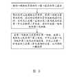
图3是本技术方案实施例触摸屏的制备方法的流程示意图。FIG. 3 is a schematic flowchart of a method for manufacturing a touch screen according to an embodiment of the technical solution.
图4是本技术方案实施例碳纳米管层中的絮状碳纳米管的扫描电镜图。Fig. 4 is a scanning electron microscope image of the flocculent carbon nanotubes in the carbon nanotube layer of the embodiment of the technical solution.
图5是本技术方案实施例显示装置的侧视结构示意图。Fig. 5 is a schematic side view structural diagram of a display device according to an embodiment of the technical solution.
具体实施方式Detailed ways
以下将结合附图详细说明本技术方案实施例提供的触摸屏、触摸屏的制备方法及使用该触摸屏的显示装置。The touch screen, the manufacturing method of the touch screen and the display device using the touch screen provided by the embodiment of the technical solution will be described in detail below with reference to the accompanying drawings.
请参阅图1及图2,本技术方案实施例提供一种触摸屏10,该触摸屏10包括一第一电极板12,一第二电极板14以及设置在第一电极板12与第二电极板14之间的多个透明点状隔离物16。Please refer to FIG. 1 and FIG. 2 , the embodiment of the present technical solution provides a
该第一电极板12包括一第一基体120,一第一导电层122以及两个第一电极124。该第一基体120为平面结构,该第一导电层122与两个第一电极124均设置在第一基体120的下表面。两个第一电极124分别设置在第一导电层122沿第一方向的两端并与第一导电层122电连接。该第二电极板14包括一第二基体140,一第二导电层142以及两个第二电极144。该第二基体140为平面结构,该第二导电层142与两个第二电极144均设置在第二基体140的上表面。两个第二电极144分别设置在第二导电层142沿第二方向的两端并与第二导电层142电连接。该第一方向垂直于该第二方向,即两个第一电极124与两个第二电极144正交设置。其中,该第一基体120为透明的且具有一定柔软度的薄膜或薄板,该第二基体140为透明基板,该第二基体140的材料可选择为玻璃、石英、金刚石及塑料等硬性材料或柔性材料。所述第二基体140主要起支撑的作用。该第一电极124与该第二电极144的材料为金属、碳纳米管薄膜或其他导电材料,只要确保导电性即可。本实施例中,该第一基体120为聚酯膜,该第二基体140为玻璃基板,该第一电极124与第二电极144为导电的银浆层。The
进一步地,该第二电极板14上表面外围设置有一绝缘层18。上述的第一电极板12设置在该绝缘层18上,且该第一电极板12的第一导电层122正对第二电极板14的第二导电层142设置。上述多个透明点状隔离物16设置在第二电极板14的第二导电层142上,且该多个透明点状隔离物16彼此间隔设置。第一电极板12与第二电极板14之间的距离为2~10微米。该绝缘层18与透明点状隔离物16均可采用绝缘透明树脂或其他绝缘透明材料制成。设置绝缘层18与透明点状隔离物16可使得第一电极板14与第二电极板12电绝缘。可以理解,当触摸屏10尺寸较小时,透明点状隔离物16为可选择的结构,只需确保第一电极板14与第二电极板12电绝缘即可。Further, an
该第一导电层122与第二导电层142中的至少一个导电层包括一碳纳米管层。进一步地,该碳纳米管层可以为一个碳纳米管薄膜,该碳纳米管薄膜包括相互缠绕的碳纳米管,所述碳纳米管之间通过范德华力相互吸引、缠绕,形成网络状结构。所述碳纳米管薄膜中,碳纳米管为各向同性,均匀分布,无规则排列,形成大量的微孔结构,微孔孔径小于10微米。上述碳纳米管层的长度和宽度不限,可根据实际需要制成具有任意长度和宽度的碳纳米管层。另外,上述碳纳米管层的厚度也不限,在确保透光性的前提下,可根据实际需要制成具有任意厚度的碳纳米管层。上述碳纳米管薄膜中的碳纳米管包括单壁碳纳米管、双壁碳纳米管和多壁碳纳米管。当碳纳米管薄膜中的碳纳米管为单壁碳纳米管时,该单壁碳纳米管的直径为0.5纳米~50纳米。当碳纳米管薄膜中的碳纳米管为双壁碳纳米管时,该双壁碳纳米管的直径为1.0纳米~50纳米。当碳纳米管薄膜中的碳纳米管为多壁碳纳米管时,该多壁碳纳米管的直径为1.5纳米~50纳米。At least one conductive layer of the first conductive layer 122 and the second
由于碳纳米管相互缠绕,因此所述碳纳米管薄膜具有很好的韧性,可以弯曲折叠成任意形状而不破裂。本技术方案实施例中的碳纳米管薄膜为一平面结构。Since the carbon nanotubes are intertwined, the carbon nanotube film has good toughness and can be bent and folded into any shape without breaking. The carbon nanotube film in the embodiment of the technical solution has a planar structure.
另外,该第一电极板12上表面可进一步设置一透明保护膜126,该透明保护膜126可由氮化硅、氧化硅、苯丙环丁烯(BCB)、聚酯膜以及丙烯酸树脂等材料形成。该透明保护膜126也可采用一层表面硬化处理、光滑防刮的塑料层,如聚对苯二甲酸乙二醇酯(PET)膜,用于保护第一电极板12,提高耐用性。该透明保护膜126还可用于提供一些其它的附加功能,如可以减少眩光或降低反射。In addition, a transparent
此外,可选择地,为了减小由显示设备产生的电磁干扰,避免从触摸屏10发出的信号产生错误,还可在第二基体140的下表面上设置一屏蔽层(图未示)。该屏蔽层可由铟锡氧化物(ITO)薄膜、锑锡氧化物(ATO)薄膜、镍金薄膜、银薄膜或碳纳米管层等透明导电材料形成。本实施例中,所述的屏蔽层包含一碳纳米管薄膜,该碳纳米管薄膜中的碳纳米管的排列方式不限,可为各向同性,均匀分布,无规则排列也可为其它的排列方式,只需确保导电性和透光性。本实施例中,该屏蔽层中的碳纳米管各向同性,均匀分布,无规则排列。该碳纳米管薄膜作为电接地点,起到屏蔽的作用,从而使得触摸屏10能在无干扰的环境中工作。In addition, optionally, in order to reduce electromagnetic interference generated by the display device and avoid errors in signals sent from the
请参阅图3,本技术方案实施例提供一种制备上述触摸屏10的方法,具体包括以下步骤:Please refer to FIG. 3, the embodiment of the technical solution provides a method for preparing the above-mentioned
步骤一:提供一碳纳米管原料及一第一基体和第二基体。Step 1: providing a carbon nanotube raw material and a first matrix and a second matrix.
所述碳纳米管原料的获得包括以下步骤:The obtaining of the carbon nanotube raw material comprises the following steps:
首先,提供一碳纳米管阵列形成于一基底,优选地,该阵列为超顺排碳纳米管阵列。Firstly, a carbon nanotube array formed on a substrate is provided. Preferably, the array is a superparallel carbon nanotube array.
本技术方案实施例提供的碳纳米管阵列为单壁碳纳米管阵列、双壁碳纳米管阵列及多壁碳纳米管阵列中的一种。该碳纳米管阵列的制备方法采用化学气相沉积法,其具体步骤包括:(a)提供一平整基底,该基底可选用P型或N型硅基底,或选用形成有氧化层的硅基底,本实施例优选为采用4英寸的硅基底;(b)在基底表面均匀形成一催化剂层,该催化剂层材料可选用铁(Fe)、钴(Co)、镍(Ni)或其任意组合的合金之一;(c)将上述形成有催化剂层的基底在700℃~900℃的空气中退火约30分钟~90分钟;(d)将处理过的基底置于反应炉中,在保护气体环境下加热到500℃~740℃,然后通入碳源气体反应约5分钟~30分钟,生长得到碳纳米管阵列,其高度大于10微米。该碳纳米管阵列为多个彼此平行且垂直于基底生长的碳纳米管形成的纯碳纳米管阵列。该碳纳米管阵列与上述基底面积基本相同。通过上述控制生长条件,该超顺排碳纳米管阵列中基本不含有杂质,如无定型碳或残留的催化剂金属颗粒等。The carbon nanotube array provided in the embodiment of the technical solution is one of a single-wall carbon nanotube array, a double-wall carbon nanotube array and a multi-wall carbon nanotube array. The preparation method of the carbon nanotube array adopts a chemical vapor deposition method, and its specific steps include: (a) providing a flat substrate, which can be a P-type or N-type silicon substrate, or a silicon substrate formed with an oxide layer. The embodiment preferably adopts a silicon substrate of 4 inches; (b) uniformly forms a catalyst layer on the surface of the substrate, and the catalyst layer material can be selected from iron (Fe), cobalt (Co), nickel (Ni) or an alloy of any combination thereof 1; (c) annealing the above-mentioned substrate formed with the catalyst layer in air at 700° C. to 900° C. for about 30 minutes to 90 minutes; (d) placing the treated substrate in a reaction furnace and heating it under a protective gas environment to 500° C. to 740° C., and then pass through carbon source gas to react for about 5 minutes to 30 minutes, and grow to obtain a carbon nanotube array, the height of which is greater than 10 microns. The carbon nanotube array is a pure carbon nanotube array formed by a plurality of carbon nanotubes growing parallel to each other and perpendicular to the substrate. The carbon nanotube array has substantially the same area as the aforementioned substrate. By controlling the growth conditions above, the super-aligned carbon nanotube array basically does not contain impurities, such as amorphous carbon or residual catalyst metal particles.
其次,采用刀片或其他工具将上述碳纳米管阵列中的碳纳米管从基底刮落,获得一碳纳米管原料,其中上述碳纳米管在一定程度上保持相互缠绕的状态。所述的碳纳米管原料中,碳纳米管的长度大于10微米。Secondly, the carbon nanotubes in the carbon nanotube array are scraped off from the substrate by using a blade or other tools to obtain a carbon nanotube raw material, wherein the carbon nanotubes are intertwined to a certain extent. In the carbon nanotube raw material, the length of the carbon nanotube is greater than 10 microns.
本技术方案实施例中碳源气可选用乙炔、乙烯、甲烷等化学性质较活泼的碳氢化合物,本技术方案实施例优选的碳源气为乙炔;保护气体为氮气或惰性气体,本技术方案实施例优选的保护气体为氩气。In the embodiment of the technical solution, the carbon source gas can be selected from acetylene, ethylene, methane and other chemically active hydrocarbons. The preferred carbon source gas in the embodiment of the technical solution is acetylene; the protective gas is nitrogen or an inert gas. Examples The preferred protective gas is argon.
可以理解,本技术方案实施例提供的碳纳米管阵列不限于上述制备方法。It can be understood that the carbon nanotube array provided in the embodiment of the technical solution is not limited to the above-mentioned preparation method.
所述第一基体120和第二基体140的材料为玻璃、石英、金刚石及塑料等硬性材料或柔性材料。本实施例中,该第一基体120为聚酯膜,该第二基体140为玻璃基板。The materials of the
步骤二:絮化处理上述碳纳米管原料,获得一碳纳米管絮状结构,通过对该碳纳米管絮状结构进行处理,分别在上述第一基体120和第二基体140表面形成第一导电层122和第二导电层142,进而形成第一电极板12和第二电极板14。Step 2: flocculation treatment of the above-mentioned carbon nanotube raw materials to obtain a carbon nanotube flocculation structure, and by processing the carbon nanotube flocculation structure, a first conductive layer is formed on the surface of the
所述絮化处理上述碳纳米管原料的步骤为将上述碳纳米管原料添加到一溶剂中通过超声波分散处理或高强度搅拌等方法来处理所述碳纳米管原料,获得一碳纳米管絮状结构。本技术方案实施例中,所述溶剂可选用水、易挥发的有机溶剂等。优选地,本技术方案实施例采用在水中超声波分散所述碳纳米管原料10~30分钟。由于碳纳米管具有极大的比表面积,相互缠绕的碳纳米管之间具有较大的范德华力。上述絮化处理并不会将该碳纳米管原料中的碳纳米管完全分散在溶剂中,碳纳米管之间通过范德华力相互吸引、缠绕,形成网络状结构。The step of flocculating the above-mentioned carbon nanotube raw material is to add the above-mentioned carbon nanotube raw material into a solvent to process the carbon nanotube raw material through ultrasonic dispersion treatment or high-intensity stirring to obtain a carbon nanotube flocculent structure. In the embodiment of the technical solution, the solvent may be water, a volatile organic solvent, or the like. Preferably, in the embodiment of the technical solution, ultrasonic waves are used to disperse the carbon nanotube raw material in water for 10-30 minutes. Due to the large specific surface area of carbon nanotubes, there is a large van der Waals force between intertwined carbon nanotubes. The above flocculation treatment does not completely disperse the carbon nanotubes in the carbon nanotube raw material in the solvent, and the carbon nanotubes attract and entangle with each other through van der Waals force to form a network structure.
本技术方案实施例中,所述通过对上述碳纳米管絮状结构进行处理形成第一导电层122和一第二导电层142的步骤包括以下两种形成方式:其一,通过抽滤的方式获得一碳纳米管层;将所述碳纳米管层粘结在所述第一基体120和第二基体140表面形成上述第一导电层122和第二导电层142。其二,分离所述碳纳米管絮状结构;将上述碳纳米管絮状结构按照所述第一基体120和第二基体140的形状摊开在所述第一基体120和第二基体140上,施加一定压力于摊开的碳纳米管絮状结构;以及,将该碳纳米管絮状结构中残留的溶剂烘干或等溶剂自然挥发后形成上述第一导电层122和第二导电层142。In the embodiment of the technical solution, the step of forming the first conductive layer 122 and a second
本技术方案实施例中,所述的直接通过抽滤的方式获得一碳纳米管层的步骤具体包括以下步骤:提供一微孔滤膜及一抽气漏斗;将上述含有碳纳米管絮状结构的溶剂经过该微孔滤膜倒入该抽气漏斗中;抽滤并干燥后获得一碳纳米管层。该微孔滤膜为一表面光滑、孔径为0.22微米的滤膜。由于抽滤方式本身将提供一较大的气压作用于该碳纳米管絮状结构,该碳纳米管絮状结构经过抽滤会直接形成一均匀的碳纳米管层。且,由于微孔滤膜表面光滑,该碳纳米管层容易剥离。该碳纳米管层可通过粘结剂粘结在所述第一基体120和第二基体140表面。In the embodiment of the technical solution, the step of directly obtaining a carbon nanotube layer by means of suction filtration specifically includes the following steps: providing a microporous filter membrane and a suction funnel; The solvent is poured into the suction funnel through the microporous filter membrane; a carbon nanotube layer is obtained after suction filtration and drying. The microporous filter membrane is a filter membrane with a smooth surface and a pore size of 0.22 microns. Since the suction filtration method itself will provide a large air pressure to act on the carbon nanotube floc structure, the carbon nanotube floc structure will directly form a uniform carbon nanotube layer after suction filtration. Moreover, because the surface of the microporous membrane is smooth, the carbon nanotube layer is easy to peel off. The carbon nanotube layer can be bonded to the surfaces of the
本技术方案实施例中,所述的分离碳纳米管絮状结构的步骤具体包括以下步骤:将上述含有碳纳米管絮状结构的溶剂倒入一放有滤纸的漏斗中;静置干燥一段时间从而获得一分离的碳纳米管絮状结构。上述的碳纳米管在碳纳米管絮状结构中相互缠绕成不规则的絮状结构。In the embodiment of the technical solution, the step of separating the carbon nanotube floc structure specifically includes the following steps: pour the above-mentioned solvent containing the carbon nanotube floc structure into a funnel with filter paper; let stand and dry for a period of time Thus, a separated carbon nanotube floc structure is obtained. The above-mentioned carbon nanotubes are intertwined in the carbon nanotube floc structure to form an irregular floc structure.
可以理解,也可将分离后的碳纳米管絮状结构摊开在一基板上,施加一定压力于摊开的碳纳米管絮状结构,以及,将该碳纳米管絮状结构中残留的溶剂烘干或等溶剂自然挥发后形成一碳纳米管层,然后将该碳纳米管层切割成基体大小形状的碳纳米管层,分别粘结在所述第一基体120和第二基体140上形成上述第一导电层122和第二导电层142。It can be understood that the separated carbon nanotube floc structure can also be spread on a substrate, and a certain pressure can be applied to the spread carbon nanotube floc structure, and the residual solvent in the carbon nanotube floc structure Dry or wait for the solvent to volatilize naturally to form a carbon nanotube layer, and then cut the carbon nanotube layer into carbon nanotube layers of the size and shape of the substrate, and bond them to the
可以理解,本技术方案实施例可通过控制该碳纳米管絮状结构摊开的面积来控制该碳纳米管薄膜的厚度和面密度。碳纳米管絮状结构摊开的面积越大,则该碳纳米管薄膜的厚度和面密度就越小。施加的压力的大小可控制上述絮状结构摊开面积的大小。进一步地,还可对上述的碳纳米管薄膜进行切割,从而形成一预定形状的碳纳米管层。所述碳纳米管薄膜的厚度为0.5纳米-100微米。It can be understood that in the embodiment of the technical solution, the thickness and surface density of the carbon nanotube film can be controlled by controlling the spread area of the carbon nanotube flocculent structure. The larger the spread area of the carbon nanotube floc structure, the smaller the thickness and surface density of the carbon nanotube film. The size of the applied pressure can control the size of the spread area of the above-mentioned flocculent structure. Furthermore, the above-mentioned carbon nanotube film can also be cut to form a carbon nanotube layer with a predetermined shape. The carbon nanotube film has a thickness of 0.5 nanometers to 100 micrometers.
本实施例中,所述碳纳米管薄膜的长度为30厘米,宽度为30厘米,厚度为1微米,所述碳纳米管薄膜的微观形貌请参阅图4,且,该碳纳米管薄膜包括相互缠绕的碳纳米管。In this embodiment, the length of the carbon nanotube film is 30 centimeters, the width is 30 centimeters, and the thickness is 1 micron. Please refer to Figure 4 for the microscopic appearance of the carbon nanotube film, and the carbon nanotube film includes Intertwined carbon nanotubes.
本技术方案实施例制备的碳纳米管层中包括相互缠绕的碳纳米管,所述碳纳米管之间通过范德华力相互吸引、缠绕,形成网络状结构,因此该碳纳米管层具有很好的韧性。在该碳纳米管层中,碳纳米管为各向同性,均匀分布,无规则排列,形成大量的微孔结构,微孔孔径小于10微米。The carbon nanotube layer prepared by the embodiment of the technical solution includes intertwined carbon nanotubes, and the carbon nanotubes are attracted and entangled with each other through van der Waals force to form a network structure, so the carbon nanotube layer has a good toughness. In the carbon nanotube layer, the carbon nanotubes are isotropic, uniformly distributed and randomly arranged to form a large number of microporous structures, and the diameter of the micropores is less than 10 microns.
步骤三:在第一电极板12上设置两个第一电极124,在第二电极板14上设置两个第二电极144,并将上述第一电极板12和第二电极板14间隔设置,且使上述第一导电层122和上述第二导电层142相对设置,从而得到一触摸屏10。Step 3: setting two first electrodes 124 on the
本技术方案实施例中,所述两个第一电极124和两个第二电极144均为导电的银浆层。所述两个第一电极124和两个第二电极144的形成方法为:采用丝网印刷、移印或喷涂等方式分别将银浆涂覆在所述第一导电层142沿第一方向的两端及第二导电层142沿第二方向的两端,然后,将第一电极板和第二电极板分别放入烘箱中烘烤10-60分钟使银浆固化,烘烤温度为100℃-120℃,即可得到所述第一电极124及所述第二电极144。上述第一方向垂直于上述第二方向,即两个第一电极124与两个第二电极144正交设置。In the embodiment of the technical solution, the two first electrodes 124 and the two second electrodes 144 are conductive silver paste layers. The forming method of the two first electrodes 124 and the two second electrodes 144 is: respectively apply silver paste on the first
所述绝缘层18可采用绝缘树脂或其他绝缘材料制成,如绝缘粘合剂。本技术方案实施例中,该绝缘层18为绝缘粘合剂。所述第一电极板12和所述第二电极板14通过绝缘粘合剂使彼此接合,该绝缘粘合剂可涂覆于上述第一电极板12和第二电极板14的外围。此外,多个点状隔离物16可设置在上述绝缘粘合剂所在区域之外的可视区内,以确保上述第一电极板12和第二电极板14电绝缘。The insulating
该透明保护膜126可为一层表面硬化处理、光滑防刮的塑料层,如聚对苯二甲酸乙二醇酯(PET)膜,用于保护第一电极板12,提高耐用性。本技术方案实施例中,该透明保护膜126采用有粘性的PET膜,该PET膜可直接粘附于触摸屏表面用作透明保护膜。The transparent
请参阅图5,本技术方案实施例还提供一使用上述触摸屏10的显示装置100,其包括上述触摸屏10及一显示设备20。该显示设备20正对且靠近上述触摸屏10的第二电极板14设置。该触摸屏10可以与该显示设备20间隔一预定距离设置,也可集成在该显示设备20上。当该触摸屏10与该显示设备20集成设置时,可通过粘结剂将该触摸屏10附着到该显示设备20上。Please refer to FIG. 5 , the embodiment of the technical solution further provides a
本技术方案显示设备20可以为液晶显示器、场发射显示器、等离子显示器、电致发光显示器、真空荧光显示器及阴极射线管等显示设备。The
进一步地,当在该触摸屏10第二基体140的下表面上设置一屏蔽层22时,可在该屏蔽层22远离第二基体140的表面上设置一钝化层24,该钝化层24可由氮化硅、氧化硅等材料形成。该钝化层24与显示设备20的正面间隔一间隙26设置。该钝化层24作为介电层使用,且保护该显示设备20不致于由于外力过大而损坏。Further, when a
另外,该显示装置100进一步包括一触摸屏控制器30、一中央处理器40及一显示设备控制器50。其中,该触摸屏控制器30、该中央处理器40及该显示设备控制器50三者通过电路相互连接,该触摸屏控制器30与该触摸屏20电连接,该显示设备控制器50与该显示设备20电连接。该触摸屏控制器30通过手指等触摸物60触摸的图标或菜单位置来定位选择信息输入,并将该信息传递给中央处理器40。该中央处理器40通过该显示器控制器50控制该显示元件20显示。In addition, the
使用时,第一电极板12之间与第二电极板14之间分别施加5V电压。使用者一边视觉确认在触摸屏10下面设置的显示元件20的显示,一边通过触摸物60如手指或笔按压触摸屏10第一电极板12进行操作。第一电极板12中第一基体120发生弯曲,使得按压处70的第一导电层122与第二电极板14的第二导电层142接触形成导通。触摸屏控制器30通过分别测量第一导电层122第一方向上的电压变化与第二导电层142第二方向上的电压变化,并进行精确计算,将它转换成触点坐标。触摸屏控制器30将数字化的触点坐标传递给中央处理器40。中央处理器40根据触点坐标发出相应指令,启动电子设备的各种功能切换,并通过显示器控制器50控制显示元件20显示。In use, a voltage of 5V is applied between the
与现有技术相比较,本技术方案实施例提供的采用碳纳米管层作为透明导电层的触摸屏、触摸屏的制造方法及显示装置具有以下优点:其一,由于碳纳米管在所述的碳纳米管层中通过范德华力相互吸引、缠绕,形成网络状结构,从而使得上述的碳纳米管层具有较好的机械强度和韧性,故,采用上述的碳纳米管层作透明导电层,可以相应的提高触摸屏的耐用性,进而提高显示装置的耐用性;其二,上述碳纳米管层中的碳纳米管薄膜包含多个碳纳米管,且上述的碳纳米管在每一碳纳米管薄膜中各向同性、均匀分布、无规则排列,形成大量的微孔结构,微孔孔径小于10微米。故,采用上述的碳纳米管层作透明导电层,可使得透明导电层具有均匀的阻值分布和较好的透光特性,从而提高触摸屏及使用该触摸屏的显示装置的分辨率和精确度。其三,由于碳纳米管层中的碳纳米管薄膜是通过将碳纳米管原料进行絮化处理获得,且该碳纳米管层可直接铺设在基体上形成透明导电层,制备方法简单且无需真空环境和加热过程,故采用上述方法制备的碳纳米管薄膜所形成的碳纳米管层做透明导电层有利于降低触摸屏及使用该触摸屏的显示装置的成本。Compared with the prior art, the touch screen using the carbon nanotube layer as the transparent conductive layer, the manufacturing method of the touch screen, and the display device provided by the embodiment of the technical solution have the following advantages: First, since the carbon nanotube layer is in the carbon nanotube The tube layer attracts and entangles with each other through van der Waals force to form a network structure, so that the above-mentioned carbon nanotube layer has good mechanical strength and toughness. Therefore, using the above-mentioned carbon nanotube layer as a transparent conductive layer can correspond to Improve the durability of the touch screen, and then improve the durability of the display device; secondly, the carbon nanotube film in the above-mentioned carbon nanotube layer contains a plurality of carbon nanotubes, and the above-mentioned carbon nanotubes are in each carbon nanotube film. Isotropic, evenly distributed, and randomly arranged, forming a large number of microporous structures, the pore size of which is less than 10 microns. Therefore, using the above-mentioned carbon nanotube layer as the transparent conductive layer can make the transparent conductive layer have uniform resistance distribution and better light transmission characteristics, thereby improving the resolution and accuracy of the touch screen and the display device using the touch screen. Third, since the carbon nanotube film in the carbon nanotube layer is obtained by flocculating the carbon nanotube raw material, and the carbon nanotube layer can be directly laid on the substrate to form a transparent conductive layer, the preparation method is simple and does not require vacuum Environment and heating process, so the carbon nanotube layer formed by the carbon nanotube film prepared by the above method is used as a transparent conductive layer, which is beneficial to reduce the cost of the touch screen and the display device using the touch screen.
另外,本领域技术人员还可在本发明精神内作其它变化,当然这些依据本发明精神所作的变化,都应包含在本发明所要求保护的范围内。In addition, those skilled in the art can also make other changes within the spirit of the present invention. Of course, these changes made according to the spirit of the present invention should be included in the scope of protection claimed by the present invention.
Claims (29)
Priority Applications (8)
| Application Number | Priority Date | Filing Date | Title |
|---|---|---|---|
| CN2007101251079ACN101458606B (en) | 2007-12-12 | 2007-12-12 | Touch screen, method for producing the touch screen, and display device using the touch screen |
| US12/286,228US8542212B2 (en) | 2007-12-12 | 2008-09-29 | Touch panel, method for making the same, and display device adopting the same |
| EP08253437AEP2053496A3 (en) | 2007-10-23 | 2008-10-22 | Touch panel and display device adopting the same |
| KR1020080104437AKR101210701B1 (en) | 2007-10-23 | 2008-10-23 | Touch panel, method for making the same, and electronic device adopting the same |
| JP2008317351AJP4965549B2 (en) | 2007-12-12 | 2008-12-12 | Touch panel and manufacturing method thereof, display using touch panel |
| US13/954,978US9262032B2 (en) | 2007-12-12 | 2013-07-31 | Method for making touch panel |
| US14/981,994US10268329B2 (en) | 2007-12-12 | 2015-12-29 | Method for making touch panel |
| US16/295,507US11372509B2 (en) | 2007-12-12 | 2019-03-07 | Method for making touch panel |
Applications Claiming Priority (1)
| Application Number | Priority Date | Filing Date | Title |
|---|---|---|---|
| CN2007101251079ACN101458606B (en) | 2007-12-12 | 2007-12-12 | Touch screen, method for producing the touch screen, and display device using the touch screen |
Publications (2)
| Publication Number | Publication Date |
|---|---|
| CN101458606A CN101458606A (en) | 2009-06-17 |
| CN101458606Btrue CN101458606B (en) | 2012-06-20 |
Family
ID=40752572
Family Applications (1)
| Application Number | Title | Priority Date | Filing Date |
|---|---|---|---|
| CN2007101251079AActiveCN101458606B (en) | 2007-10-23 | 2007-12-12 | Touch screen, method for producing the touch screen, and display device using the touch screen |
Country Status (3)
| Country | Link |
|---|---|
| US (4) | US8542212B2 (en) |
| JP (1) | JP4965549B2 (en) |
| CN (1) | CN101458606B (en) |
Families Citing this family (45)
| Publication number | Priority date | Publication date | Assignee | Title |
|---|---|---|---|---|
| CN101620454A (en)* | 2008-07-04 | 2010-01-06 | 清华大学 | Potable computer |
| CN101458606B (en)* | 2007-12-12 | 2012-06-20 | 清华大学 | Touch screen, method for producing the touch screen, and display device using the touch screen |
| CN101458593B (en)* | 2007-12-12 | 2012-03-14 | 清华大学 | Touch screen and display device |
| CN101458597B (en)* | 2007-12-14 | 2011-06-08 | 清华大学 | Touch screen, method for producing the touch screen, and display device using the touch screen |
| CN101655720B (en)* | 2008-08-22 | 2012-07-18 | 清华大学 | Personal digital assistant |
| CN101458600B (en)* | 2007-12-14 | 2011-11-30 | 清华大学 | Touch screen and display device |
| CN101458608B (en)* | 2007-12-14 | 2011-09-28 | 清华大学 | Touch screen preparation method |
| CN101458594B (en)* | 2007-12-12 | 2012-07-18 | 清华大学 | Touch screen and display device |
| CN101656769B (en)* | 2008-08-22 | 2012-10-10 | 清华大学 | Mobile telephone |
| CN101458599B (en)* | 2007-12-14 | 2011-06-08 | 清华大学 | Touch screen, method for producing the touch screen, and display device using the touch screen |
| CN101676832B (en)* | 2008-09-19 | 2012-03-28 | 清华大学 | Desktop PC |
| CN101458603B (en)* | 2007-12-12 | 2011-06-08 | 北京富纳特创新科技有限公司 | Touch screen and display device |
| CN101419519B (en) | 2007-10-23 | 2012-06-20 | 清华大学 | Touch panel |
| CN101464763B (en)* | 2007-12-21 | 2010-09-29 | 清华大学 | Manufacturing method of touch screen |
| CN101458975B (en)* | 2007-12-12 | 2012-05-16 | 清华大学 | Electronic element |
| CN101458607B (en)* | 2007-12-14 | 2010-12-29 | 清华大学 | Touch screen and display device |
| CN101470565B (en)* | 2007-12-27 | 2011-08-24 | 清华大学 | Touch screen and display device |
| US8574393B2 (en) | 2007-12-21 | 2013-11-05 | Tsinghua University | Method for making touch panel |
| CN101464765B (en)* | 2007-12-21 | 2011-01-05 | 鸿富锦精密工业(深圳)有限公司 | Touch screen and display equipment |
| US8390580B2 (en) | 2008-07-09 | 2013-03-05 | Tsinghua University | Touch panel, liquid crystal display screen using the same, and methods for making the touch panel and the liquid crystal display screen |
| CN101924816B (en) | 2009-06-12 | 2013-03-20 | 清华大学 | Flexible mobile phone |
| CN101989136B (en)* | 2009-08-07 | 2012-12-19 | 清华大学 | Touch screen and display device |
| CN101995988B (en)* | 2009-08-19 | 2012-08-15 | 群康科技(深圳)有限公司 | Touch screen |
| FI127197B (en)* | 2009-09-04 | 2018-01-31 | Canatu Oy | Touch screen and method of manufacturing a touch screen |
| CN102214021B (en)* | 2010-04-02 | 2013-05-29 | 北京富纳特创新科技有限公司 | Touch display device |
| TWI481923B (en)* | 2010-06-24 | 2015-04-21 | Beijing Funate Innovation Tech | Touch liquid crystal display |
| TWI417771B (en)* | 2010-06-24 | 2013-12-01 | Beijing Funate Innovation Tech | touch screen |
| CN101880035A (en) | 2010-06-29 | 2010-11-10 | 清华大学 | carbon nanotube structure |
| KR101219597B1 (en)* | 2010-10-18 | 2013-01-08 | 엘지이노텍 주식회사 | Touch Screen Panel and Fabricating Method for the Same |
| CN102073428B (en)* | 2011-01-07 | 2013-02-13 | 中国科学院苏州纳米技术与纳米仿生研究所 | Capacitance type flexible and transparent touch screen based on CNT film |
| CN103094526B (en)* | 2011-10-28 | 2015-07-29 | 清华大学 | The preparation method of lithium ion cell positive |
| CN103094525B (en)* | 2011-10-28 | 2016-08-03 | 清华大学 | Lithium ion battery negative and preparation method thereof |
| CN103295667A (en)* | 2012-02-23 | 2013-09-11 | 群康科技(深圳)有限公司 | Composite conductive structure, manufacturing method thereof and display and touch panel with composite conductive structure |
| KR101945439B1 (en)* | 2012-04-24 | 2019-02-11 | 삼성디스플레이 주식회사 | flexible touch screen panel |
| CN103576230A (en)* | 2012-07-23 | 2014-02-12 | 天津富纳源创科技有限公司 | Polaroid |
| WO2014018115A1 (en) | 2012-07-26 | 2014-01-30 | Changello Enterprise Llc | Ultrasound-based force sensing of inputs |
| WO2014018121A1 (en) | 2012-07-26 | 2014-01-30 | Changello Enterprise Llc | Fingerprint-assisted force estimation |
| WO2014018116A1 (en) | 2012-07-26 | 2014-01-30 | Changello Enterprise Llc | Ultrasound-based force sensing and touch sensing |
| DE112013003674T5 (en)* | 2012-07-26 | 2015-04-30 | Apple Inc. | Force detection by an ultrasonic sensor |
| WO2014035479A2 (en) | 2012-08-30 | 2014-03-06 | Changello Enterprise Llc | Auto-baseline determination for force sensing |
| CN105807970B (en)* | 2014-12-31 | 2018-08-17 | 清华大学 | Hovering control device |
| CN105807971B (en)* | 2014-12-31 | 2019-01-18 | 清华大学 | Electrostatic transducer |
| KR102312260B1 (en) | 2015-01-09 | 2021-10-13 | 삼성디스플레이 주식회사 | Flexible touch panel and flexible display device |
| CN106487952A (en)* | 2015-08-27 | 2017-03-08 | 合肥杰事杰新材料股份有限公司 | A kind of radiating cell phone rear cover |
| KR101982289B1 (en)* | 2017-09-21 | 2019-05-24 | 고려대학교 산학협력단 | Carbon nanotube elelctron emitter, method for manufacturing the same and x-ray source using the same |
Citations (1)
| Publication number | Priority date | Publication date | Assignee | Title |
|---|---|---|---|---|
| CN1947203A (en)* | 2004-04-20 | 2007-04-11 | 他喜龙株式会社 | Touch panel-use transparent conductive molded product and touch panel |
Family Cites Families (197)
| Publication number | Priority date | Publication date | Assignee | Title |
|---|---|---|---|---|
| JPS61231626A (en) | 1985-04-05 | 1986-10-15 | Asahi Chem Ind Co Ltd | Conductive sheet for position detection |
| US4659873A (en) | 1985-07-19 | 1987-04-21 | Elographics, Inc. | Fabric touch sensor and method of manufacture |
| JPH0350177Y2 (en) | 1985-10-11 | 1991-10-25 | ||
| JPS62182916U (en) | 1986-05-08 | 1987-11-20 | ||
| JPH0344004Y2 (en) | 1986-05-26 | 1991-09-17 | ||
| US4853498A (en) | 1988-06-13 | 1989-08-01 | Tektronix, Inc. | Position measurement apparatus for capacitive touch panel system |
| US4933660A (en) | 1989-10-27 | 1990-06-12 | Elographics, Inc. | Touch sensor with touch pressure capability |
| EP0435438B1 (en) | 1989-12-28 | 1998-03-04 | Gunze Limited | Input system including resistance film touch panel |
| US5296043A (en)* | 1990-02-16 | 1994-03-22 | Canon Kabushiki Kaisha | Multi-cells integrated solar cell module and process for producing the same |
| JPH0628090Y2 (en) | 1992-06-03 | 1994-08-03 | 健一 古谷 | Electrode structure in used needle processing equipment |
| US5861583A (en) | 1992-06-08 | 1999-01-19 | Synaptics, Incorporated | Object position detector |
| JPH06339252A (en) | 1993-05-27 | 1994-12-06 | Mabuchi Motor Co Ltd | Rotation detecting device for small dc motor |
| TW242732B (en) | 1993-06-29 | 1995-03-11 | Victor Company Of Japan | Digital chrominance signal processing circuit |
| JPH08222893A (en) | 1995-02-17 | 1996-08-30 | Japan Tobacco Inc | Workpiece mounting machine suction nozzle |
| US6373472B1 (en) | 1995-10-13 | 2002-04-16 | Silviu Palalau | Driver control interface system |
| US5853877A (en) | 1996-05-31 | 1998-12-29 | Hyperion Catalysis International, Inc. | Method for disentangling hollow carbon microfibers, electrically conductive transparent carbon microfibers aggregation film amd coating for forming such film |
| TW341684B (en) | 1996-07-15 | 1998-10-01 | Synaptics Inc | Object position detector |
| JP3861333B2 (en) | 1996-08-27 | 2006-12-20 | 松下電器産業株式会社 | Coordinate position input device |
| US7663607B2 (en) | 2004-05-06 | 2010-02-16 | Apple Inc. | Multipoint touchscreen |
| JP3309851B2 (en) | 1998-05-15 | 2002-07-29 | 東洋紡績株式会社 | Transparent conductive film and touch panel |
| US5931764A (en) | 1998-06-24 | 1999-08-03 | Viztec, Inc. | Wearable device with flexible display |
| US6664950B1 (en) | 1999-11-17 | 2003-12-16 | L-3 Communications | Resistive touch panel using removable, tensioned top layer |
| JP2001222378A (en) | 2000-02-10 | 2001-08-17 | Nec Saitama Ltd | Touch panel input device |
| JP2001267782A (en) | 2000-03-21 | 2001-09-28 | Shimadzu Corp | Electromagnetic wave absorption shielding material |
| TW521227B (en) | 2000-03-31 | 2003-02-21 | Sharp Kk | Electrode substrate, method for producing the same and display device including the same |
| KR100698898B1 (en) | 2000-08-03 | 2007-03-22 | 한국터치스크린(주) | Touch panel |
| US6423583B1 (en) | 2001-01-03 | 2002-07-23 | International Business Machines Corporation | Methodology for electrically induced selective breakdown of nanotubes |
| TW521259B (en) | 2001-01-11 | 2003-02-21 | Atouch Co Ltd | Flat panel display with input device |
| JP2002278701A (en) | 2001-03-21 | 2002-09-27 | Nissha Printing Co Ltd | Touch panel |
| WO2002076724A1 (en) | 2001-03-26 | 2002-10-03 | Eikos, Inc. | Coatings containing carbon nanotubes |
| TW508652B (en) | 2001-10-03 | 2002-11-01 | Taiwan Semiconductor Mfg | Device and method for wafer drying |
| JP3798287B2 (en) | 2001-10-10 | 2006-07-19 | Smk株式会社 | Touch panel input device |
| WO2003049219A1 (en)* | 2001-11-30 | 2003-06-12 | The Trustees Of Boston College | Coated carbon nanotube array electrodes |
| KR100840670B1 (en) | 2001-12-27 | 2008-06-24 | 엘지디스플레이 주식회사 | Touch panel integrated liquid crystal display panel |
| KR20030055856A (en) | 2001-12-27 | 2003-07-04 | 엘지.필립스 엘시디 주식회사 | Fabricated Method Of Liquid Crystal Display Apparatus Integrated Film Type Touch Panel |
| KR100796489B1 (en) | 2001-12-28 | 2008-01-21 | 엘지.필립스 엘시디 주식회사 | Touch panel device and manufacturing method thereof |
| JP4051988B2 (en) | 2002-04-09 | 2008-02-27 | 富士ゼロックス株式会社 | Photoelectric conversion element and photoelectric conversion device |
| CN2539375Y (en) | 2002-04-15 | 2003-03-05 | 湖南三才光电信息材料有限公司 | High-stable flexible transparent conducting composite film |
| AU2003229333A1 (en) | 2002-05-21 | 2003-12-12 | Eikos, Inc. | Method for patterning carbon nanotube coating and carbon nanotube wiring |
| JP3877302B2 (en)* | 2002-06-24 | 2007-02-07 | 本田技研工業株式会社 | Method for forming carbon nanotube |
| US7405774B2 (en) | 2002-08-20 | 2008-07-29 | Samsung Electronics Co., Ltd. | Light guide plate and liquid crystal display having the same |
| AU2003251307A1 (en)* | 2002-09-10 | 2004-04-30 | The Trustees Of The University Pennsylvania | Carbon nanotubes: high solids dispersions and nematic gels thereof |
| CN1281982C (en) | 2002-09-10 | 2006-10-25 | 清华大学 | Polarized element and method for manufacturing same |
| CN100411979C (en) | 2002-09-16 | 2008-08-20 | 清华大学 | A carbon nanotube rope and its manufacturing method |
| KR100459230B1 (en) | 2002-11-14 | 2004-12-03 | 엘지.필립스 엘시디 주식회사 | touch panel for display device |
| KR100451773B1 (en) | 2002-11-20 | 2004-10-08 | 엘지.필립스 엘시디 주식회사 | Touch Panel in Digital Resistive Type |
| JP2004189573A (en) | 2002-12-13 | 2004-07-08 | Jfe Engineering Kk | Aggregate of carbon nanotubes and carbon nanotube installation device having the same |
| CN1286715C (en) | 2002-12-21 | 2006-11-29 | 清华大学 | Carbon nanometer tube array structure and growing method thereof |
| KR100685954B1 (en) | 2002-12-24 | 2007-02-23 | 엘지.필립스 엘시디 주식회사 | Touch panel |
| CN1321885C (en) | 2003-01-23 | 2007-06-20 | 南昌大学 | Method for preparing film of tube of directed nano carbon on soft base |
| JP2004230690A (en) | 2003-01-30 | 2004-08-19 | Takiron Co Ltd | Antistatic transparent resin sheet |
| JP2007112133A (en) | 2003-01-30 | 2007-05-10 | Takiron Co Ltd | Electroconductive shaped article |
| JP4471346B2 (en) | 2003-01-31 | 2010-06-02 | タキロン株式会社 | Electromagnetic shield |
| JP4572543B2 (en) | 2003-02-14 | 2010-11-04 | 東レ株式会社 | Field effect transistor and liquid crystal display device using the same |
| KR100509763B1 (en) | 2003-03-11 | 2005-08-25 | 엘지전자 주식회사 | Front filter of plasma display panel |
| CN1186745C (en) | 2003-03-18 | 2005-01-26 | 中国电子科技集团公司第五十五研究所 | High reliable touch screen and manufacturing technique |
| US7150865B2 (en) | 2003-03-31 | 2006-12-19 | Honda Giken Kogyo Kabushiki Kaisha | Method for selective enrichment of carbon nanotubes |
| FR2854409B1 (en)* | 2003-04-30 | 2005-06-17 | Centre Nat Rech Scient | PROCESS FOR OBTAINING FIBERS HAVING A HIGH CONTENT OF COLLOIDAL PARTICLES AND COMPOSITE FIBERS OBTAINED |
| JP4586334B2 (en) | 2003-05-07 | 2010-11-24 | ソニー株式会社 | Field effect transistor and manufacturing method thereof |
| CN2638143Y (en) | 2003-05-24 | 2004-09-01 | 江阴市华丽计算机网络工程有限公司 | Multifunctional PDA |
| GB0313808D0 (en) | 2003-06-14 | 2003-07-23 | Binstead Ronald P | Improvements in touch technology |
| JP2005037851A (en) | 2003-06-24 | 2005-02-10 | Seiko Epson Corp | Electrophoretic dispersion liquid, electrophoretic display device, electrophoretic display device manufacturing method, and electronic apparatus |
| CN1315362C (en) | 2003-06-27 | 2007-05-09 | 中国科学院上海硅酸盐研究所 | Carbon nano-pipe/ceramic composite material possessing microwave absorption function and its preparation method |
| JP4325479B2 (en) | 2003-07-17 | 2009-09-02 | セイコーエプソン株式会社 | Organic transistor manufacturing method, active matrix device manufacturing method, display device manufacturing method, and electronic device manufacturing method |
| TWI249134B (en) | 2003-07-23 | 2006-02-11 | Wintek Corp | Touch panel structure |
| JP2005056604A (en) | 2003-08-06 | 2005-03-03 | Hitachi Displays Ltd | Self-luminous flat panel display |
| CN1284727C (en)* | 2003-11-07 | 2006-11-15 | 中国科学院化学研究所 | Method for chemically modifying carbon nanotubes |
| JP4415653B2 (en) | 2003-11-19 | 2010-02-17 | セイコーエプソン株式会社 | Thin film transistor manufacturing method |
| JP4804711B2 (en) | 2003-11-21 | 2011-11-02 | 株式会社 日立ディスプレイズ | Image display device |
| JP4038685B2 (en) | 2003-12-08 | 2008-01-30 | 独立行政法人科学技術振興機構 | Actuator element |
| US20050209392A1 (en) | 2003-12-17 | 2005-09-22 | Jiazhong Luo | Polymer binders for flexible and transparent conductive coatings containing carbon nanotubes |
| JP2005182339A (en) | 2003-12-18 | 2005-07-07 | Kawaguchiko Seimitsu Co Ltd | Touch panel and screen input type display device therewith |
| JP4336592B2 (en) | 2004-02-04 | 2009-09-30 | シチズンホールディングス株式会社 | Position input device |
| US7604843B1 (en)* | 2005-03-16 | 2009-10-20 | Nanosolar, Inc. | Metallic dispersion |
| JP2005286158A (en) | 2004-03-30 | 2005-10-13 | Seiko Epson Corp | PATTERN FORMING METHOD, ELECTRONIC DEVICE, ITS MANUFACTURING METHOD, AND ELECTRONIC DEVICE |
| CN1960943B (en) | 2004-04-19 | 2013-01-02 | 独立行政法人科学技术振兴机构 | Carbon-based fine structure group, aggregate of carbon based fine structure, use thereof and method for preparation thereof |
| CN1690915A (en) | 2004-04-28 | 2005-11-02 | 秦建忠 | Double screen notebook computer |
| TWI261716B (en) | 2004-05-13 | 2006-09-11 | Quanta Display Inc | Liquid crystal display apparatus and fabrication thereof |
| JP2008500933A (en) | 2004-05-14 | 2008-01-17 | ソニー ドイチュラント ゲゼルシャフト ミット ベシュレンクテル ハフツング | Composite material comprising carbon nanotube and metal carbonate |
| US8127440B2 (en)* | 2006-10-16 | 2012-03-06 | Douglas Joel S | Method of making bondable flexible printed circuit |
| CN2706973Y (en) | 2004-06-30 | 2005-06-29 | 陈凯 | Fingers-nipping gloves cell phone |
| CN1998067B (en) | 2004-07-06 | 2010-07-14 | 毫微-专卖股份有限公司 | Activation of carbon nanotubes in field emission applications |
| ES2555309T3 (en) | 2004-07-06 | 2015-12-30 | Maricare Oy | Sensor product for electric field detection |
| US7194912B2 (en) | 2004-07-13 | 2007-03-27 | United States Of America As Represented By The Administrator Of The National Aeronautics And Space Administration | Carbon nanotube-based sensor and method for continually sensing changes in a structure |
| US7129097B2 (en) | 2004-07-29 | 2006-10-31 | International Business Machines Corporation | Integrated circuit chip utilizing oriented carbon nanotube conductive layers |
| JP4539241B2 (en) | 2004-09-02 | 2010-09-08 | パナソニック株式会社 | Touch panel and manufacturing method thereof |
| TWI249708B (en) | 2004-09-09 | 2006-02-21 | Ind Tech Res Inst | Analog resistive touch panel without bias |
| US7345296B2 (en) | 2004-09-16 | 2008-03-18 | Atomate Corporation | Nanotube transistor and rectifying devices |
| US20070298253A1 (en) | 2004-09-17 | 2007-12-27 | Kenji Hata | Transparent Conductive Carbon Nanotube Film and a Method for Producing the Same |
| JP4639714B2 (en) | 2004-09-17 | 2011-02-23 | セイコーエプソン株式会社 | Liquid crystal display device and portable information terminal equipped with the liquid crystal display device |
| US7573547B2 (en) | 2004-09-27 | 2009-08-11 | Idc, Llc | System and method for protecting micro-structure of display array using spacers in gap within display device |
| WO2006046656A1 (en)* | 2004-10-28 | 2006-05-04 | Mitsubishi Chemical Corporation | Spherical carbon particles and aggregate thereof |
| JP2006171336A (en) | 2004-12-15 | 2006-06-29 | Takiron Co Ltd | Transparent electrode member for image display, and the image display device |
| TWI339290B (en) | 2004-12-31 | 2011-03-21 | Hon Hai Prec Ind Co Ltd | Liquid crystal display device |
| US8223444B2 (en) | 2005-01-07 | 2012-07-17 | Olympus Corporation | Medium exhibiting negative refraction, optical element, and optical system |
| US20060262055A1 (en) | 2005-01-26 | 2006-11-23 | Toshiba Matsushita Display Technology | Plane display device |
| TWI258708B (en) | 2005-01-27 | 2006-07-21 | Apex Material Technology Corp | Resistive touch panel, and it manufacturing method |
| JP5028744B2 (en) | 2005-02-15 | 2012-09-19 | 富士通株式会社 | Method for forming carbon nanotube and method for manufacturing electronic device |
| TWI267014B (en) | 2005-02-21 | 2006-11-21 | Au Optronics Corp | Organic light emitting diode display |
| US20060188721A1 (en) | 2005-02-22 | 2006-08-24 | Eastman Kodak Company | Adhesive transfer method of carbon nanotube layer |
| JP4679182B2 (en) | 2005-03-04 | 2011-04-27 | 株式会社シーズ・ラボ | Map display method, map display program, and map display device |
| US20060213251A1 (en) | 2005-03-24 | 2006-09-28 | University Of Florida Research Foundation, Inc. | Carbon nanotube films for hydrogen sensing |
| JP2006269311A (en) | 2005-03-25 | 2006-10-05 | Toray Ind Inc | Transparent conductive film containing carbon nano-tube obtained by making metal-carrying carrier contact with carbon-containing organic compound |
| JP4965835B2 (en)* | 2005-03-25 | 2012-07-04 | キヤノン株式会社 | Structure, manufacturing method thereof, and device using the structure |
| TWI253846B (en) | 2005-03-28 | 2006-04-21 | Ind Tech Res Inst | Photo-sensing display unit |
| US7656365B2 (en)* | 2005-03-28 | 2010-02-02 | Chad Byron Moore | Double-sided fiber-based displays |
| JP2006285068A (en) | 2005-04-04 | 2006-10-19 | Nikkiso Co Ltd | Conductive polarizing film |
| KR100770258B1 (en) | 2005-04-22 | 2007-10-25 | 삼성에스디아이 주식회사 | Organic thin film transistor and its manufacturing method |
| JP2006310154A (en) | 2005-04-28 | 2006-11-09 | Bussan Nanotech Research Institute Inc | Transparent conductive film and coating composition for transparent conductive film |
| JP5288441B2 (en) | 2005-05-10 | 2013-09-11 | 住友精密工業株式会社 | High thermal conductive composite material and its manufacturing method |
| WO2008063148A2 (en)* | 2005-05-20 | 2008-05-29 | University Of Central Florida | Carbon nanotube reinforced metal composites |
| US7633583B2 (en) | 2005-05-23 | 2009-12-15 | Ran-Hong Raymond Wang | Controlling polarization for liquid crystal displays |
| DE102006023993A1 (en) | 2005-05-23 | 2007-03-08 | Wang, Ran-Hong, Tustin | Polarization control for liquid crystal displays |
| JP2006330883A (en) | 2005-05-24 | 2006-12-07 | Gunze Ltd | Haze adjusting film and touch panel using it |
| EP1892609A4 (en) | 2005-05-26 | 2013-03-27 | Gunze Kk | Transparent planar body and transparent touch switch |
| US7535462B2 (en) | 2005-06-02 | 2009-05-19 | Eastman Kodak Company | Touchscreen with one carbon nanotube conductive layer |
| US7593004B2 (en) | 2005-06-02 | 2009-09-22 | Eastman Kodak Company | Touchscreen with conductive layer comprising carbon nanotubes |
| US7645497B2 (en) | 2005-06-02 | 2010-01-12 | Eastman Kodak Company | Multi-layer conductor with carbon nanotubes |
| US8545790B2 (en) | 2005-06-04 | 2013-10-01 | Gregory Konesky | Cross-linked carbon nanotubes |
| WO2006132254A1 (en) | 2005-06-07 | 2006-12-14 | Kuraray Co., Ltd. | Carbon nanotube dispersion liquid and transparent conductive film using same |
| JP2008210528A (en) | 2005-06-16 | 2008-09-11 | Nissha Printing Co Ltd | Casing with illuminated switch and its manufacturing method |
| JP2007011997A (en)* | 2005-07-04 | 2007-01-18 | Fujitsu Component Ltd | Touch panel |
| JP2007018226A (en) | 2005-07-07 | 2007-01-25 | Three M Innovative Properties Co | Touch panel sensor |
| WO2007012899A1 (en) | 2005-07-25 | 2007-02-01 | Plastic Logic Limited | Flexible touch screen display |
| CN1903793A (en) | 2005-07-26 | 2007-01-31 | 中国科学院物理研究所 | Carbon silicon composite material, its preparation method and use |
| EP2477230B1 (en) | 2005-08-12 | 2015-02-25 | Cambrios Technologies Corporation | Nanowires-based transparent conductors on a flexible donor substrate |
| CN100336192C (en) | 2005-08-18 | 2007-09-05 | 上海交通大学 | Method for bonding nanometer material on metal electrode |
| JP2007123870A (en) | 2005-09-29 | 2007-05-17 | Matsushita Electric Ind Co Ltd | Flat panel display device and manufacturing method thereof |
| CN100543905C (en) | 2005-09-30 | 2009-09-23 | 北京富纳特创新科技有限公司 | A field emission device and its preparation method |
| US7995777B2 (en) | 2005-10-03 | 2011-08-09 | Xun Yu | Thin film transparent acoustic transducer |
| US20070085838A1 (en) | 2005-10-17 | 2007-04-19 | Ricks Theodore K | Method for making a display with integrated touchscreen |
| CN100412654C (en)* | 2005-10-27 | 2008-08-20 | 清华大学 | Liquid crystal display device and manufacturing method thereof |
| TWI297088B (en) | 2005-10-28 | 2008-05-21 | Hon Hai Prec Ind Co Ltd | Liquid crystal display and its manufacturing method |
| CN100427388C (en) | 2005-11-25 | 2008-10-22 | 清华大学 | A large-area ultra-thin carbon nanotube film and its preparation process |
| CN101317205B (en) | 2005-11-29 | 2010-11-03 | 精工电子有限公司 | Process for producing display and method of laminating |
| TWI386420B (en) | 2005-12-06 | 2013-02-21 | Mitsubishi Rayon Co | Carbon nanotube structure, composite and manufacturing method thereof |
| TW200722559A (en) | 2005-12-06 | 2007-06-16 | Ind Tech Res Inst | Metal nanodot arrays and fabrication methods thereof |
| JP4908136B2 (en) | 2005-12-06 | 2012-04-04 | 三菱レイヨン株式会社 | Carbon nanotube-containing composition, composite, and production method thereof |
| CN2844974Y (en) | 2005-12-08 | 2006-12-06 | 比亚迪股份有限公司 | Contact style liquid crystal display device |
| CN100462301C (en) | 2005-12-09 | 2009-02-18 | 清华大学 | A kind of preparation method of carbon nanotube array |
| CN100500556C (en) | 2005-12-16 | 2009-06-17 | 清华大学 | Carbon nanotube filament and method for making the same |
| US8264137B2 (en) | 2006-01-03 | 2012-09-11 | Samsung Electronics Co., Ltd. | Curing binder material for carbon nanotube electron emission cathodes |
| TW200727163A (en) | 2006-01-06 | 2007-07-16 | Pan Jit Internat Inc | Antibacterial touch display device |
| JP5050352B2 (en) | 2006-01-10 | 2012-10-17 | Nok株式会社 | Post-treatment method for carbon material thin film |
| US8421755B2 (en) | 2006-01-17 | 2013-04-16 | World Properties, Inc. | Capacitive touch sensor with integral EL backlight |
| JP4779681B2 (en) | 2006-02-07 | 2011-09-28 | パナソニック株式会社 | Touch panel |
| KR20070081902A (en) | 2006-02-14 | 2007-08-20 | 삼성전자주식회사 | Liquid crystal display |
| JP2007229989A (en) | 2006-02-28 | 2007-09-13 | Takiron Co Ltd | Conductive molded body and its manufacturing method |
| JP4968854B2 (en) | 2006-02-28 | 2012-07-04 | 東洋紡績株式会社 | Carbon nanotube aggregate, carbon nanotube fiber, and method for producing carbon nanotube fiber |
| TWM306694U (en) | 2006-03-15 | 2007-02-21 | Ushine Photonics Corp | Durable resistive touch screen |
| TWI308290B (en) | 2006-03-17 | 2009-04-01 | Innolux Display Corp | Touch panel |
| TWI331374B (en) | 2006-03-23 | 2010-10-01 | Unimicron Technology Corp | Carbon nanotube field emitting display |
| JP4799237B2 (en) | 2006-03-27 | 2011-10-26 | 三洋電機株式会社 | Displacement detection sensor, displacement detection device, and terminal device |
| US20090056854A1 (en) | 2006-04-04 | 2009-03-05 | Top-Nanosis, Inc. | Method for manufacturing conductive composite material |
| JP2007310869A (en) | 2006-04-17 | 2007-11-29 | Matsushita Electric Ind Co Ltd | Input device control method and input device used therefor |
| CN101059738A (en) | 2006-04-20 | 2007-10-24 | 铼宝科技股份有限公司 | Transparent touch screen with upward-emitting organic light-emitting diodes |
| GB2437827B (en) | 2006-05-05 | 2008-03-26 | Harald Philipp | Touch screen element |
| KR20070113763A (en) | 2006-05-26 | 2007-11-29 | 삼성전자주식회사 | Carbon nanotube pattern forming method and carbon nanotube pattern obtained thereby |
| US7796123B1 (en) | 2006-06-20 | 2010-09-14 | Eastman Kodak Company | Touchscreen with carbon nanotube conductive layers |
| US7630041B2 (en) | 2006-06-23 | 2009-12-08 | Tsinghua University | Liquid crystal cell assembly for liquid crystal display |
| US20080048996A1 (en) | 2006-08-11 | 2008-02-28 | Unidym, Inc. | Touch screen devices employing nanostructure networks |
| KR20060129977A (en) | 2006-09-08 | 2006-12-18 | 아이티엠 주식회사 | Highly durable resistive touch screen panel and its manufacturing method |
| KR100790216B1 (en) | 2006-10-17 | 2008-01-02 | 삼성전자주식회사 | CNC Transparent Electrode Using Conductive Dispersant and Manufacturing Method Thereof |
| CN100450922C (en) | 2006-11-10 | 2009-01-14 | 清华大学 | Ultralong orientational carbon nano-tube filament/film and its preparation method |
| JP4350740B2 (en) | 2006-12-05 | 2009-10-21 | レノボ・シンガポール・プライベート・リミテッド | Portable electronic device, method for changing display direction of screen, program, and storage medium |
| CN100405617C (en) | 2006-12-29 | 2008-07-23 | 清华大学 | Solar cell based on carbon nanotube film and preparation method thereof |
| US20080192014A1 (en) | 2007-02-08 | 2008-08-14 | Tyco Electronics Corporation | Touch screen using carbon nanotube electrodes |
| CN101239712B (en) | 2007-02-09 | 2010-05-26 | 清华大学 | Carbon nanotube film structure and preparation method thereof |
| WO2008127780A2 (en) | 2007-02-21 | 2008-10-23 | Nantero, Inc. | Symmetric touch screen system with carbon nanotube-based transparent conductive electrode pairs |
| CN101276012B (en) | 2007-03-30 | 2016-04-27 | 清华大学 | Polarizing element and its preparation method |
| CN101280161B (en) | 2007-04-06 | 2013-01-09 | 清华大学 | Conducting adhesive tape and manufacturing method thereof |
| US20080266273A1 (en) | 2007-04-24 | 2008-10-30 | White Electronic Designs Corp. | Interactive display system |
| CN101315974B (en)* | 2007-06-01 | 2010-05-26 | 清华大学 | Lithium-ion battery negative electrode and preparation method thereof |
| KR20090023803A (en) | 2007-09-03 | 2009-03-06 | 삼성전자주식회사 | Liquid crystal display panel and manufacturing method thereof |
| CN101458606B (en) | 2007-12-12 | 2012-06-20 | 清华大学 | Touch screen, method for producing the touch screen, and display device using the touch screen |
| CN101458597B (en) | 2007-12-14 | 2011-06-08 | 清华大学 | Touch screen, method for producing the touch screen, and display device using the touch screen |
| CN101419519B (en) | 2007-10-23 | 2012-06-20 | 清华大学 | Touch panel |
| CN101419518B (en) | 2007-10-23 | 2012-06-20 | 清华大学 | Touch panel |
| CN101458594B (en) | 2007-12-12 | 2012-07-18 | 清华大学 | Touch screen and display device |
| CN101458599B (en)* | 2007-12-14 | 2011-06-08 | 清华大学 | Touch screen, method for producing the touch screen, and display device using the touch screen |
| CN101620454A (en) | 2008-07-04 | 2010-01-06 | 清华大学 | Potable computer |
| CN101458593B (en) | 2007-12-12 | 2012-03-14 | 清华大学 | Touch screen and display device |
| TWI351119B (en) | 2007-12-14 | 2011-10-21 | Hon Hai Prec Ind Co Ltd | Touch panel and displaying device using the same |
| TWI364860B (en) | 2007-12-21 | 2012-05-21 | Hon Hai Prec Ind Co Ltd | Touch panel, method for making the same, and displaying device adopting the same |
| TWI357167B (en) | 2007-12-21 | 2012-01-21 | Hon Hai Prec Ind Co Ltd | Touch panel, method for making the same, and displ |
| CN101470565B (en) | 2007-12-27 | 2011-08-24 | 清华大学 | Touch screen and display device |
| JP2008102968A (en) | 2007-12-28 | 2008-05-01 | Fujitsu Component Ltd | Touch panel |
| TWI354921B (en) | 2007-12-31 | 2011-12-21 | Hon Hai Prec Ind Co Ltd | Touch panel and displaying device using the same |
| CN101582448B (en) | 2008-05-14 | 2012-09-19 | 清华大学 | thin film transistor |
| US8132468B2 (en) | 2008-05-29 | 2012-03-13 | Zoran Radivojevic | Flexural deformation sensing device and a user interface using the same |
| US8237677B2 (en) | 2008-07-04 | 2012-08-07 | Tsinghua University | Liquid crystal display screen |
| US8390580B2 (en) | 2008-07-09 | 2013-03-05 | Tsinghua University | Touch panel, liquid crystal display screen using the same, and methods for making the touch panel and the liquid crystal display screen |
| TWI373727B (en) | 2008-07-25 | 2012-10-01 | Hon Hai Prec Ind Co Ltd | Portable computer |
| CN101989136B (en) | 2009-08-07 | 2012-12-19 | 清华大学 | Touch screen and display device |
| CN102115071B (en)* | 2009-12-31 | 2013-01-09 | 清华大学 | Film spreading system and method for spreading films by using same |
| CN102463715B (en)* | 2010-10-29 | 2014-03-26 | 清华大学 | Method for preparing carbon nano-tube composite material and application thereof |
| CN102222764B (en)* | 2011-06-24 | 2013-11-20 | 清华大学 | Method for manufacturing phase change memory |
- 2007
- 2007-12-12CNCN2007101251079Apatent/CN101458606B/enactiveActive
- 2008
- 2008-09-29USUS12/286,228patent/US8542212B2/enactiveActive
- 2008-12-12JPJP2008317351Apatent/JP4965549B2/enactiveActive
- 2013
- 2013-07-31USUS13/954,978patent/US9262032B2/enactiveActive
- 2015
- 2015-12-29USUS14/981,994patent/US10268329B2/enactiveActive
- 2019
- 2019-03-07USUS16/295,507patent/US11372509B2/enactiveActive
Patent Citations (1)
| Publication number | Priority date | Publication date | Assignee | Title |
|---|---|---|---|---|
| CN1947203A (en)* | 2004-04-20 | 2007-04-11 | 他喜龙株式会社 | Touch panel-use transparent conductive molded product and touch panel |
Non-Patent Citations (1)
| Title |
|---|
| JP特开2007-11997A 2007.01.18 |
Also Published As
| Publication number | Publication date |
|---|---|
| JP2009146416A (en) | 2009-07-02 |
| US20160117025A1 (en) | 2016-04-28 |
| US8542212B2 (en) | 2013-09-24 |
| US20090153516A1 (en) | 2009-06-18 |
| US20190204960A1 (en) | 2019-07-04 |
| US11372509B2 (en) | 2022-06-28 |
| US10268329B2 (en) | 2019-04-23 |
| US20130312252A1 (en) | 2013-11-28 |
| CN101458606A (en) | 2009-06-17 |
| US9262032B2 (en) | 2016-02-16 |
| JP4965549B2 (en) | 2012-07-04 |
Similar Documents
| Publication | Publication Date | Title |
|---|---|---|
| CN101458606B (en) | Touch screen, method for producing the touch screen, and display device using the touch screen | |
| TWI357167B (en) | Touch panel, method for making the same, and displ | |
| CN101458597B (en) | Touch screen, method for producing the touch screen, and display device using the touch screen | |
| CN101470558B (en) | Touch screen and display equipment | |
| CN101419519B (en) | Touch panel | |
| CN101419518B (en) | Touch panel | |
| CN101458607B (en) | Touch screen and display device | |
| CN101470559B (en) | Touch screen and display equipment | |
| CN101470565B (en) | Touch screen and display device | |
| CN101458608B (en) | Touch screen preparation method | |
| CN101458599B (en) | Touch screen, method for producing the touch screen, and display device using the touch screen | |
| CN101458603B (en) | Touch screen and display device | |
| CN101458594A (en) | Touch screen and display device | |
| CN101464765A (en) | Touch screen and display equipment | |
| CN101464763A (en) | Production method of touch screen | |
| CN101458602B (en) | Touch screen and display device | |
| CN101458595B (en) | Touch screen and display device | |
| CN101458604B (en) | Touch screen and display device | |
| CN101464766B (en) | Touch screen and display equipment | |
| TWI386831B (en) | Touch panel and displaying device using the same | |
| TW200928913A (en) | Touch panel and displaying device using the same | |
| TWI500194B (en) | Touch screen, method for preparing touch screen, and display device using the same | |
| CN101458605A (en) | Touch screen and display device | |
| TW200929642A (en) | Touch panel, method for making the same, and displaying device adopting the same | |
| TW200928902A (en) | Touch panel and displaying device using the same |
Legal Events
| Date | Code | Title | Description |
|---|---|---|---|
| C06 | Publication | ||
| PB01 | Publication | ||
| C10 | Entry into substantive examination | ||
| SE01 | Entry into force of request for substantive examination | ||
| C14 | Grant of patent or utility model | ||
| GR01 | Patent grant |