CN101449347A - Capacitive micro- electro-mechanical sensors with single crystal silicon electrodes - Google Patents
Capacitive micro- electro-mechanical sensors with single crystal silicon electrodesDownload PDFInfo
- Publication number
- CN101449347A CN101449347ACNA2007800178712ACN200780017871ACN101449347ACN 101449347 ACN101449347 ACN 101449347ACN A2007800178712 ACNA2007800178712 ACN A2007800178712ACN 200780017871 ACN200780017871 ACN 200780017871ACN 101449347 ACN101449347 ACN 101449347A
- Authority
- CN
- China
- Prior art keywords
- layer
- sensor
- capacitive
- electrode
- single crystal
- Prior art date
- Legal status (The legal status is an assumption and is not a legal conclusion. Google has not performed a legal analysis and makes no representation as to the accuracy of the status listed.)
- Granted
Links
Images


Classifications
- G—PHYSICS
- G01—MEASURING; TESTING
- G01L—MEASURING FORCE, STRESS, TORQUE, WORK, MECHANICAL POWER, MECHANICAL EFFICIENCY, OR FLUID PRESSURE
- G01L9/00—Measuring steady of quasi-steady pressure of fluid or fluent solid material by electric or magnetic pressure-sensitive elements; Transmitting or indicating the displacement of mechanical pressure-sensitive elements, used to measure the steady or quasi-steady pressure of a fluid or fluent solid material, by electric or magnetic means
- G01L9/0041—Transmitting or indicating the displacement of flexible diaphragms
- G01L9/0072—Transmitting or indicating the displacement of flexible diaphragms using variations in capacitance
- G01L9/0073—Transmitting or indicating the displacement of flexible diaphragms using variations in capacitance using a semiconductive diaphragm
- B—PERFORMING OPERATIONS; TRANSPORTING
- B81—MICROSTRUCTURAL TECHNOLOGY
- B81B—MICROSTRUCTURAL DEVICES OR SYSTEMS, e.g. MICROMECHANICAL DEVICES
- B81B3/00—Devices comprising flexible or deformable elements, e.g. comprising elastic tongues or membranes
- B81B3/0018—Structures acting upon the moving or flexible element for transforming energy into mechanical movement or vice versa, i.e. actuators, sensors, generators
- B81B3/0021—Transducers for transforming electrical into mechanical energy or vice versa
- G—PHYSICS
- G01—MEASURING; TESTING
- G01P—MEASURING LINEAR OR ANGULAR SPEED, ACCELERATION, DECELERATION, OR SHOCK; INDICATING PRESENCE, ABSENCE, OR DIRECTION, OF MOVEMENT
- G01P15/00—Measuring acceleration; Measuring deceleration; Measuring shock, i.e. sudden change of acceleration
- G01P15/02—Measuring acceleration; Measuring deceleration; Measuring shock, i.e. sudden change of acceleration by making use of inertia forces using solid seismic masses
- G01P15/08—Measuring acceleration; Measuring deceleration; Measuring shock, i.e. sudden change of acceleration by making use of inertia forces using solid seismic masses with conversion into electric or magnetic values
- G01P15/0802—Details
- G—PHYSICS
- G01—MEASURING; TESTING
- G01P—MEASURING LINEAR OR ANGULAR SPEED, ACCELERATION, DECELERATION, OR SHOCK; INDICATING PRESENCE, ABSENCE, OR DIRECTION, OF MOVEMENT
- G01P15/00—Measuring acceleration; Measuring deceleration; Measuring shock, i.e. sudden change of acceleration
- G01P15/02—Measuring acceleration; Measuring deceleration; Measuring shock, i.e. sudden change of acceleration by making use of inertia forces using solid seismic masses
- G01P15/08—Measuring acceleration; Measuring deceleration; Measuring shock, i.e. sudden change of acceleration by making use of inertia forces using solid seismic masses with conversion into electric or magnetic values
- G01P15/125—Measuring acceleration; Measuring deceleration; Measuring shock, i.e. sudden change of acceleration by making use of inertia forces using solid seismic masses with conversion into electric or magnetic values by capacitive pick-up
- G—PHYSICS
- G01—MEASURING; TESTING
- G01P—MEASURING LINEAR OR ANGULAR SPEED, ACCELERATION, DECELERATION, OR SHOCK; INDICATING PRESENCE, ABSENCE, OR DIRECTION, OF MOVEMENT
- G01P15/00—Measuring acceleration; Measuring deceleration; Measuring shock, i.e. sudden change of acceleration
- G01P15/18—Measuring acceleration; Measuring deceleration; Measuring shock, i.e. sudden change of acceleration in two or more dimensions
- B—PERFORMING OPERATIONS; TRANSPORTING
- B81—MICROSTRUCTURAL TECHNOLOGY
- B81B—MICROSTRUCTURAL DEVICES OR SYSTEMS, e.g. MICROMECHANICAL DEVICES
- B81B2201/00—Specific applications of microelectromechanical systems
- B81B2201/02—Sensors
- B81B2201/0228—Inertial sensors
- B81B2201/0235—Accelerometers
- B—PERFORMING OPERATIONS; TRANSPORTING
- B81—MICROSTRUCTURAL TECHNOLOGY
- B81B—MICROSTRUCTURAL DEVICES OR SYSTEMS, e.g. MICROMECHANICAL DEVICES
- B81B2201/00—Specific applications of microelectromechanical systems
- B81B2201/02—Sensors
- B81B2201/0228—Inertial sensors
- B81B2201/0242—Gyroscopes
- B—PERFORMING OPERATIONS; TRANSPORTING
- B81—MICROSTRUCTURAL TECHNOLOGY
- B81B—MICROSTRUCTURAL DEVICES OR SYSTEMS, e.g. MICROMECHANICAL DEVICES
- B81B2201/00—Specific applications of microelectromechanical systems
- B81B2201/02—Sensors
- B81B2201/0264—Pressure sensors
- G—PHYSICS
- G01—MEASURING; TESTING
- G01P—MEASURING LINEAR OR ANGULAR SPEED, ACCELERATION, DECELERATION, OR SHOCK; INDICATING PRESENCE, ABSENCE, OR DIRECTION, OF MOVEMENT
- G01P15/00—Measuring acceleration; Measuring deceleration; Measuring shock, i.e. sudden change of acceleration
- G01P15/02—Measuring acceleration; Measuring deceleration; Measuring shock, i.e. sudden change of acceleration by making use of inertia forces using solid seismic masses
- G01P15/08—Measuring acceleration; Measuring deceleration; Measuring shock, i.e. sudden change of acceleration by making use of inertia forces using solid seismic masses with conversion into electric or magnetic values
- G01P2015/0805—Measuring acceleration; Measuring deceleration; Measuring shock, i.e. sudden change of acceleration by making use of inertia forces using solid seismic masses with conversion into electric or magnetic values being provided with a particular type of spring-mass-system for defining the displacement of a seismic mass due to an external acceleration
- G01P2015/0808—Measuring acceleration; Measuring deceleration; Measuring shock, i.e. sudden change of acceleration by making use of inertia forces using solid seismic masses with conversion into electric or magnetic values being provided with a particular type of spring-mass-system for defining the displacement of a seismic mass due to an external acceleration for defining in-plane movement of the mass, i.e. movement of the mass in the plane of the substrate
- G01P2015/0811—Measuring acceleration; Measuring deceleration; Measuring shock, i.e. sudden change of acceleration by making use of inertia forces using solid seismic masses with conversion into electric or magnetic values being provided with a particular type of spring-mass-system for defining the displacement of a seismic mass due to an external acceleration for defining in-plane movement of the mass, i.e. movement of the mass in the plane of the substrate for one single degree of freedom of movement of the mass
- G01P2015/0814—Measuring acceleration; Measuring deceleration; Measuring shock, i.e. sudden change of acceleration by making use of inertia forces using solid seismic masses with conversion into electric or magnetic values being provided with a particular type of spring-mass-system for defining the displacement of a seismic mass due to an external acceleration for defining in-plane movement of the mass, i.e. movement of the mass in the plane of the substrate for one single degree of freedom of movement of the mass for translational movement of the mass, e.g. shuttle type
- G—PHYSICS
- G01—MEASURING; TESTING
- G01P—MEASURING LINEAR OR ANGULAR SPEED, ACCELERATION, DECELERATION, OR SHOCK; INDICATING PRESENCE, ABSENCE, OR DIRECTION, OF MOVEMENT
- G01P15/00—Measuring acceleration; Measuring deceleration; Measuring shock, i.e. sudden change of acceleration
- G01P15/02—Measuring acceleration; Measuring deceleration; Measuring shock, i.e. sudden change of acceleration by making use of inertia forces using solid seismic masses
- G01P15/08—Measuring acceleration; Measuring deceleration; Measuring shock, i.e. sudden change of acceleration by making use of inertia forces using solid seismic masses with conversion into electric or magnetic values
- G01P2015/0805—Measuring acceleration; Measuring deceleration; Measuring shock, i.e. sudden change of acceleration by making use of inertia forces using solid seismic masses with conversion into electric or magnetic values being provided with a particular type of spring-mass-system for defining the displacement of a seismic mass due to an external acceleration
- G01P2015/0822—Measuring acceleration; Measuring deceleration; Measuring shock, i.e. sudden change of acceleration by making use of inertia forces using solid seismic masses with conversion into electric or magnetic values being provided with a particular type of spring-mass-system for defining the displacement of a seismic mass due to an external acceleration for defining out-of-plane movement of the mass
- G01P2015/0825—Measuring acceleration; Measuring deceleration; Measuring shock, i.e. sudden change of acceleration by making use of inertia forces using solid seismic masses with conversion into electric or magnetic values being provided with a particular type of spring-mass-system for defining the displacement of a seismic mass due to an external acceleration for defining out-of-plane movement of the mass for one single degree of freedom of movement of the mass
- G01P2015/0831—Measuring acceleration; Measuring deceleration; Measuring shock, i.e. sudden change of acceleration by making use of inertia forces using solid seismic masses with conversion into electric or magnetic values being provided with a particular type of spring-mass-system for defining the displacement of a seismic mass due to an external acceleration for defining out-of-plane movement of the mass for one single degree of freedom of movement of the mass the mass being of the paddle type having the pivot axis between the longitudinal ends of the mass, e.g. see-saw configuration
- G—PHYSICS
- G01—MEASURING; TESTING
- G01P—MEASURING LINEAR OR ANGULAR SPEED, ACCELERATION, DECELERATION, OR SHOCK; INDICATING PRESENCE, ABSENCE, OR DIRECTION, OF MOVEMENT
- G01P15/00—Measuring acceleration; Measuring deceleration; Measuring shock, i.e. sudden change of acceleration
- G01P15/02—Measuring acceleration; Measuring deceleration; Measuring shock, i.e. sudden change of acceleration by making use of inertia forces using solid seismic masses
- G01P15/08—Measuring acceleration; Measuring deceleration; Measuring shock, i.e. sudden change of acceleration by making use of inertia forces using solid seismic masses with conversion into electric or magnetic values
- G01P2015/0805—Measuring acceleration; Measuring deceleration; Measuring shock, i.e. sudden change of acceleration by making use of inertia forces using solid seismic masses with conversion into electric or magnetic values being provided with a particular type of spring-mass-system for defining the displacement of a seismic mass due to an external acceleration
- G01P2015/0822—Measuring acceleration; Measuring deceleration; Measuring shock, i.e. sudden change of acceleration by making use of inertia forces using solid seismic masses with conversion into electric or magnetic values being provided with a particular type of spring-mass-system for defining the displacement of a seismic mass due to an external acceleration for defining out-of-plane movement of the mass
- G01P2015/084—Measuring acceleration; Measuring deceleration; Measuring shock, i.e. sudden change of acceleration by making use of inertia forces using solid seismic masses with conversion into electric or magnetic values being provided with a particular type of spring-mass-system for defining the displacement of a seismic mass due to an external acceleration for defining out-of-plane movement of the mass the mass being suspended at more than one of its sides, e.g. membrane-type suspension, so as to permit multi-axis movement of the mass
- H—ELECTRICITY
- H10—SEMICONDUCTOR DEVICES; ELECTRIC SOLID-STATE DEVICES NOT OTHERWISE PROVIDED FOR
- H10D—INORGANIC ELECTRIC SEMICONDUCTOR DEVICES
- H10D1/00—Resistors, capacitors or inductors
- H10D1/60—Capacitors
- H10D1/68—Capacitors having no potential barriers
Landscapes
- Physics & Mathematics (AREA)
- General Physics & Mathematics (AREA)
- Chemical & Material Sciences (AREA)
- Analytical Chemistry (AREA)
- Engineering & Computer Science (AREA)
- Computer Hardware Design (AREA)
- Microelectronics & Electronic Packaging (AREA)
- Pressure Sensors (AREA)
- Measuring Fluid Pressure (AREA)
- Micromachines (AREA)
- Piezo-Electric Or Mechanical Vibrators, Or Delay Or Filter Circuits (AREA)
- Gyroscopes (AREA)
Abstract
Translated fromChinese
Description
Translated fromChinese发明领域field of invention
本发明一般涉及传感器。本发明尤其涉及具有单晶硅电极的电容性微机电传感器。The present invention generally relates to sensors. In particular, the invention relates to capacitive microelectromechanical sensors with single-crystal silicon electrodes.
背景background
几个制造特征导致电容性传感器的精确度和耐久性降低。在电容间隙的顶面和底面上使用不同的材料导致该间隙的顶与底之间热失配。金属电极的使用限制了在两个晶片之间形成高温熔化接合的能力,而这限制密闭地密封器件的能力。与引线接合焊盘在同一表面上地构造压力孔导致引线键合焊盘被曝露于正被测量的粗糙介质的棘手问题。Several manufacturing features lead to reduced accuracy and durability of capacitive sensors. Using different materials on the top and bottom surfaces of the capacitive gap results in a thermal mismatch between the top and bottom of the gap. The use of metal electrodes limits the ability to form a high temperature fusion bond between the two wafers, which limits the ability to hermetically seal the device. Configuring the pressure holes on the same surface as the wire bond pads leads to the troublesome problem of the wire bond pads being exposed to the harsh media being measured.
当前的各种制造方法解决了这些关注点中的一些,但却没能解决另一些。例如,许多方法使用导电金属通孔来将电互连放到传感器的与有源传感元件相反一侧上。然而,这些制造方法具有几个缺点。例如,必须使用额外的制造步骤来图案化传感器中的导电金属通孔。此外,使用金属引起了上述复杂度。因此,在本领域中有必要开发制造允许能密闭地密封、减小或消除热失配、并限制引线接合焊盘的曝露的电容性传感器的方法。Current manufacturing methods address some of these concerns but fail to address others. For example, many approaches use conductive metal vias to place the electrical interconnect on the side of the sensor opposite the active sensing element. However, these fabrication methods have several disadvantages. For example, additional manufacturing steps must be used to pattern the conductive metal vias in the sensor. Furthermore, the use of metals introduces the aforementioned complications. Therefore, there is a need in the art to develop methods of fabricating capacitive sensors that allow for hermetic sealing, reduce or eliminate thermal mismatch, and limit exposure of wire bond pads.
发明内容Contents of the invention
本发明提供具有单晶硅电极的电容性微机电传感器。这些传感器优选感测压力、加速度、角速度、或谐振中的至少一个。这些传感器包括两层。第一层由单晶硅制成并具有顶面和底面。第一层形成至少一个电极。第二层也由单晶硅制成并具有顶面和底面。至少有一个电极是在第二层中由从该层的顶面延伸到底面的电介质材料绝缘沟槽界定。优选此绝缘沟槽形成围绕此电极的周界。第二层还优选进一步包括至少一个电保护,其中该至少一个电保护由从该第二层的顶面延伸到其底面的第二个电介质材料绝缘沟槽界定。第一层中的此至少一个电极和第二层中的此至少一个电极一起界定电容器。优选第二层的顶面被蚀刻以形成空穴,该空穴即形成电容间隙。此传感器进一步包括至少一个位于第二层的底面上的电触点。此电触点与第二层中的此至少一个电极电连接。The present invention provides capacitive microelectromechanical sensors with single crystal silicon electrodes. These sensors preferably sense at least one of pressure, acceleration, angular velocity, or resonance. These sensors consist of two layers. The first layer is made of single crystal silicon and has a top surface and a bottom surface. The first layer forms at least one electrode. The second layer is also made of single crystal silicon and has a top surface and a bottom surface. At least one electrode is bounded in the second layer by an insulating trench of dielectric material extending from the top surface of the layer to the bottom surface. Preferably the insulating trench forms a perimeter around the electrode. The second layer also preferably further comprises at least one electrical protection, wherein the at least one electrical protection is bounded by a second insulating trench of dielectric material extending from the top surface of the second layer to the bottom surface thereof. The at least one electrode in the first layer and the at least one electrode in the second layer together define a capacitor. Preferably the top surface of the second layer is etched to form cavities which form capacitive gaps. The sensor further includes at least one electrical contact on the bottom surface of the second layer. The electrical contact is electrically connected to the at least one electrode in the second layer.
在优选实施例中,第一层形成隔膜。第一层还可被蚀刻以界定谐振结构、弹簧、或标准质量。In a preferred embodiment, the first layer forms a membrane. The first layer can also be etched to define resonant structures, springs, or standard masses.
在另一优选实施例中,此传感器进一步包括第三单晶硅层,该层通过电介质层来与顶层的顶面分开。在一个实施例中,此第三层被蚀刻以界定压力孔。在此实施例中,此传感器感测压力并具有压力孔位于器件的与电触点相反一侧上的优点。In another preferred embodiment, the sensor further comprises a third monocrystalline silicon layer separated from the top surface of the top layer by a dielectric layer. In one embodiment, this third layer is etched to define pressure holes. In this embodiment, this sensor senses pressure and has the advantage that the pressure port is on the opposite side of the device from the electrical contacts.
附图简述Brief description of the drawings
通过结合附图阅读以下描述将理解本发明及其目的和优点,在附图中:The invention, together with objects and advantages thereof, will be understood by reading the following description when read in conjunction with the accompanying drawings, in which:
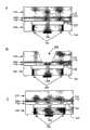
图1示出根据本发明的传感器的截面图(A)以及从其焊盘一侧观察到的平面图(B)。Figure 1 shows a cross-sectional view (A) of a sensor according to the invention and a plan view (B) viewed from its pad side.
图2示出根据本发明的传感器的示例。Figure 2 shows an example of a sensor according to the invention.
图3示出根据本发明的压力传感器的截面图(A)以及从其焊盘一侧观察到的平面图(B)。Fig. 3 shows a cross-sectional view (A) of a pressure sensor according to the present invention and a plan view (B) viewed from its pad side.
图4示出根据本发明的加速度计的截面图(A)以及从其焊盘一侧观察到的平面图(B)。Fig. 4 shows a cross-sectional view (A) of an accelerometer according to the invention and a plan view (B) viewed from its pad side.
图5示出根据本发明的加速度计梭的平面图(A)和立体图(B)。Figure 5 shows a plan view (A) and a perspective view (B) of an accelerometer shuttle according to the invention.
图6到10示出根据本发明的制造传感器的步骤的示意图。6 to 10 show schematic views of the steps of manufacturing a sensor according to the present invention.
发明的详细描述Detailed description of the invention
在以下描述中,对出现在不同附图中的结构统一标记。图1A示出根据本发明的电容性微机电传感器的截面图。该传感器包括具有顶面112和底面114的第一层110。第一层110由单晶硅制成并包含至少一个电极130。该传感器进一步包括具有顶面122和底面124的第二层120。第二层120包含由电介质材料制成的从顶面122延伸至底面124的隔离沟槽150。隔离沟槽150界定电极140。电极140电连接到诸如引线接合焊盘之类的电触点160。优选第一层110包含此传感器的所有传感元件,以使这些传感元件位于此传感器的与电触点160相反的一侧上。电极130和140一起界定具有电容间隙170的电容器。优选电容间隙170在第二层120中形成以允许精确空间界定间隙170。In the following description, structures appearing in different drawings are uniformly marked. FIG. 1A shows a cross-sectional view of a capacitive microelectromechanical sensor according to the invention. The sensor includes a
图1B示出第二层120的底面124的平面图。图1B示出隔离沟槽150形成环绕电极140的周界以界定电极140。虽然在附图中示出了方形沟槽,但是沟槽150可以是任何几何形状。FIG. 1B shows a plan view of the
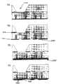
图2示出根据本发明的传感器的几个实施例。图2A示出具有第三单晶硅层210的传感器,该层210通过电介质层220来与第一层110的顶面112分开。在此传感器中,第一层110已被减薄以形成隔膜130。在优选实施例中,第三层230被蚀刻以形成压力孔230(图2B)。替换地或附加地,第一层110可被蚀刻以界定例如标准质量260、弹簧250、或谐振结构(未示出)。通过蚀刻去除电介质层220来使第一层110脱开以便能进行器件运动(图2C)。Figure 2 shows several embodiments of sensors according to the invention. FIG. 2A shows a sensor having a third
图3A示出根据本发明的优选压力传感器的截面图。该压力传感器具有第一单晶硅层110,该层已被研磨或蚀刻以形成隔膜130。隔膜130用作电容器中的第一电极。该压力传感器还具有第二单晶硅层120,该层已被蚀刻以形成空穴170。第二单晶硅层120包括两个隔离沟槽150。隔离沟槽150界定形成电容器的第二电极的固定电极340、电保护360、以及驱动公共端口370。固定电极340、电保护360和驱动公共端口370分别电连接到金属接合焊盘320、330和340。该压力传感器还具有第三单晶硅层210,该层通过电介质层220来与隔膜130分开。层220可以是例如埋入式氧化物层。层210被蚀刻以形成压力孔230。注意在该传感器中,在所有关键压力孔处都使用单晶硅,在该传感器内不需要金属,并且压力孔与敏感的金属接合焊盘相对。Figure 3A shows a cross-sectional view of a preferred pressure sensor according to the invention. The pressure sensor has a first single
图3B示出从传感器的底面看的此压力传感器的平面图。可以看到隔离沟槽150界定固定电极340、电保护360和公共驱动端口370。这些电子部件分别与金属接合焊盘320、330和340电连接。Figure 3B shows a plan view of this pressure sensor seen from the bottom surface of the sensor. It can be seen that
图4A示出根据本发明的优选加速度计的截面图,而图4B示出其平面图。在一个实施例中,该加速度计与图3中所描述的压力传感器构建在同一管芯中。该加速度计具有第一单晶硅层110,该层已被蚀刻以形成沟槽430和加速度计梭(shuttle)420。该传感器还具有第二硅层120,该层已被蚀刻以形成空穴170。第二单晶硅层120包括界定公共驱动端口460和四个电极440、442、444和450的隔离沟槽150。该公共驱动端口460和四个电极440、442、444和450分别与金属接合焊盘490、470、480、492和494电连接。该加速度计还具有第三单晶硅层210,该层通过电介质层220来与第一层130分开。层220可以是例如埋入式氧化物层。层220被蚀刻以给加速度计梭420提供间隙410。虽然所示加速度计是测量平面内加速度和平面外加速度的双轴加速度计,但通过原样复制加速度计并令其绕其平面外轴旋转90度容易实现平面内的第三轴。Figure 4A shows a cross-sectional view and Figure 4B shows a plan view of a preferred accelerometer according to the invention. In one embodiment, the accelerometer is built on the same die as the pressure sensor described in FIG. 3 . The accelerometer has a first
图5A示出加速度计梭420的平面图,而图5B示出其等角投影图。图中示出指状电极510、隔离支架515、侧向弹簧520、侧向弹簧端525、旋转弹簧530、标准质量540、万向支架550、以及隔离沟槽560。指状电极510附连到隔离支架515,而后者将与电极442或444连接。所有这些结构都是通过蚀刻第一层120形成的,如下所述。Figure 5A shows a plan view of the
图6到图10所示的步骤1到17是用于制作根据本发明的传感器的制造工艺步骤的示例的示意性描述。步骤1到3用来加工SOI(绝缘体上硅)晶片,步骤4到10用来加工隔离沟槽,而步骤11到17是双晶片加工步骤。在此示例中,这些步骤示出一种同时制造根据本发明的压力传感器和加速度计的方法。或者,通过去掉步骤2和3就能制造只感测压力的传感器。可对以下各步骤作修改以创造根据本发明的其他类型的传感器。例如,可添加并类似于表面显微机械加工地图案化多晶硅层。向层612添加这些层能使这些层在空穴730内部并且不妨碍接合表面910。
步骤1通过氧化在SOI晶片610上形成氧化物620。SOI晶片610的较薄有源层612最终形成诸如图2B中的隔膜130之类的隔膜。层612被相对重掺杂到约0.1欧姆/厘米到0.01欧姆/厘米之间以用作导电电极表面。较厚的处置层614形成图2中所描述的第三层210。步骤2通过光刻和湿法氧化蚀刻来图案化和蚀刻氧化物620以在该氧化物620中给出开口630,以使下层硅612可在步骤3中被蚀刻。步骤3是深度反应离子蚀刻(DRIE)式蚀刻以形成弹簧650、蚀刻孔640、指状电极510、隔离沟槽560、标准质量550、旋转弹簧530和隔膜层612中的其他结构(参见图5)。可在此层中通过改变掩模工艺以纳入通常可在表面显微机械加工工艺中作出的其他几何形状来制造诸如角速度传感器、谐振器、或切变传感器(shear sensor)之类的其他类型的传感器。此外,可同时制作多种类型的传感器,从而使得在一个芯片上能有更高的集成度。如本领域技术人员所理解地,可简单通过界定标准质量、弹簧和梳状驱动/梳状传感组合来制作谐振结构。步骤4再次通过氧化在包含相对重掺杂的硅的有源层712、和处置晶片714的新SOI晶片上形成氧化物720,其中该有源层712形成界定诸如图3所示的340、350和370之类的单晶硅电极的隔离沟槽,而处置晶片714则按序稍后被蚀刻掉或研磨和抛光掉。步骤5是在RIE氧化物蚀刻机中蚀刻氧化物720以在氧化物720中形成开口730。此为步骤6中的DRIE蚀刻制备有源层712。在步骤6中,有源层712从开口730被DRIE蚀刻,该蚀刻止于匣层716,从而形成沟槽740。在此蚀刻中要当心以避免产生很难填充成没有空隙的重入沟槽。在步骤7中,用热氧化物生长来氧化沟槽740以提供电介质材料750,该材料将界定和隔离单晶硅电极。在步骤8,用多晶硅810来填充沟槽740。这减少了形成隔离沟槽所需电介质材料的量。可用电介质材料填充整个沟槽,但是发现如果使用热氧化物则会因为所需的氧化物厚度而变得昂贵和困难。步骤9是使用包括DRIE、RIE或甚至桶式蚀刻机的任何类型的蚀刻机对晶片710的多晶硅覆盖层蚀刻,以从晶片710的表面除去多晶硅810,该蚀刻止于氧化物720并只在保留沟槽740的内侧上留有多晶硅810。步骤10中对硅层712约0.5微米到2微米深度的DRIE蚀刻形成诸如图2中空穴170之类的空穴730。在步骤11中使用诸如BOE(缓冲氧化蚀刻)之类的湿法蚀刻从表面910除去氧化物620和720。这使得表面910能在步骤12中使用高温晶片接合技术对准并接合。步骤11还通过底割匣层616并形成诸如图4中的间隙410之类的间隙920来使标准质量脱开。在步骤13,使用BOE在顶氧化物620中蚀刻出开口920并去除底氧化物720。这使硅层614在步骤14中能通过DRIE蚀刻被蚀刻以产生诸如图2B中的孔230之类的孔1010。还是在步骤14中,处置晶片714通过背部研磨和抛光或通过DRIE蚀刻或RIE蚀刻或桶式蚀刻机被去除。步骤15通过使用RIE氧化物蚀刻来蚀刻匣616和匣716,从而分别使隔膜612和互连1020曝露。在步骤16中,在孔1010的相反一侧使用溅射系统沉积金属1030。在步骤17中使用光刻和湿法刻蚀来蚀刻金属1030以形成互连1020和诸如图2中的接合焊盘160之类的金属接合焊盘1040。作为本领域的一名普通技术人员将理解,可作出或以其它方式实现各种改变、替换和变更而不会脱离本发明的原理。因此,应由以下权利要求书及其在法律上的等效方案来确定本发明的范围。
Claims (10)
Translated fromChineseApplications Claiming Priority (5)
| Application Number | Priority Date | Filing Date | Title |
|---|---|---|---|
| US79179006P | 2006-04-13 | 2006-04-13 | |
| US60/791,790 | 2006-04-13 | ||
| US11/707,347US7539003B2 (en) | 2005-12-01 | 2007-02-16 | Capacitive micro-electro-mechanical sensors with single crystal silicon electrodes |
| US11/707,347 | 2007-02-16 | ||
| PCT/US2007/008599WO2007120576A2 (en) | 2006-04-13 | 2007-04-04 | Capacitive micro- electro-mechanical sensors with single crystal silicon electrodes |
Publications (2)
| Publication Number | Publication Date |
|---|---|
| CN101449347Atrue CN101449347A (en) | 2009-06-03 |
| CN101449347B CN101449347B (en) | 2013-07-17 |
Family
ID=38610099
Family Applications (1)
| Application Number | Title | Priority Date | Filing Date |
|---|---|---|---|
| CN2007800178712AActiveCN101449347B (en) | 2006-04-13 | 2007-04-04 | Capacitive micro- electro-mechanical sensors with single crystal silicon electrodes |
Country Status (5)
| Country | Link |
|---|---|
| US (1) | US7539003B2 (en) |
| EP (1) | EP2011132B1 (en) |
| JP (3) | JP5331678B2 (en) |
| CN (1) | CN101449347B (en) |
| WO (1) | WO2007120576A2 (en) |
Cited By (9)
| Publication number | Priority date | Publication date | Assignee | Title |
|---|---|---|---|---|
| CN103552980A (en)* | 2013-11-15 | 2014-02-05 | 安徽北方芯动联科微系统技术有限公司 | Wafer level packaging method for micro electromechanical system (MEMS) chip and single-chip micro-miniature type MEMS chip |
| CN105084296A (en)* | 2014-04-25 | 2015-11-25 | 无锡华润上华半导体有限公司 | Manufacturing method for MEMS(Micro Electro Mechanical Systems) capacitive pressure transducer |
| CN105980293A (en)* | 2014-02-25 | 2016-09-28 | 诺思罗普·格鲁曼·利特夫有限责任公司 | Method for producing a component, and component |
| CN106030315A (en)* | 2014-02-26 | 2016-10-12 | 株式会社村田制作所 | MEMS structure with frame |
| CN108051134A (en)* | 2017-11-23 | 2018-05-18 | 胡波 | The capacitance pressure transducer, of Closed loop operation mode |
| CN104101367B (en)* | 2013-04-09 | 2018-07-24 | 霍尼韦尔国际公司 | Sensor with isolation diaphragm |
| CN108680138A (en)* | 2018-05-09 | 2018-10-19 | 中交第公路勘察设计研究院有限公司 | Soft soil foundation roadbed large deformation settlement automatic monitoring system and method |
| CN109724744A (en)* | 2013-11-06 | 2019-05-07 | 应美盛股份有限公司 | Pressure Sensor |
| CN119309558A (en)* | 2024-12-10 | 2025-01-14 | 北京晨晶电子有限公司 | An angular velocity sensor |
Families Citing this family (44)
| Publication number | Priority date | Publication date | Assignee | Title |
|---|---|---|---|---|
| US7741964B2 (en)* | 2007-05-31 | 2010-06-22 | Schrader Electronics Ltd. | Tire pressure detector having reduced power consumption mechanism |
| JP5260155B2 (en)* | 2008-06-16 | 2013-08-14 | 株式会社堀場エステック | Capacitance type pressure sensor and manufacturing method thereof |
| US8238073B2 (en)* | 2008-07-18 | 2012-08-07 | Synaptics, Inc. | In-molded capacitive sensors |
| US8499629B2 (en)* | 2008-10-10 | 2013-08-06 | Honeywell International Inc. | Mounting system for torsional suspension of a MEMS device |
| ITBO20080079U1 (en)* | 2008-10-30 | 2010-04-30 | Lorenzo Peretto | BUILDING SYSTEM FOR A CAPACITIVE SENSOR. |
| US8710599B2 (en)* | 2009-08-04 | 2014-04-29 | Fairchild Semiconductor Corporation | Micromachined devices and fabricating the same |
| US8421168B2 (en)* | 2009-11-17 | 2013-04-16 | Fairchild Semiconductor Corporation | Microelectromechanical systems microphone packaging systems |
| US8490495B2 (en) | 2010-05-05 | 2013-07-23 | Consensic, Inc. | Capacitive pressure sensor with vertical electrical feedthroughs and method to make the same |
| US9278845B2 (en) | 2010-09-18 | 2016-03-08 | Fairchild Semiconductor Corporation | MEMS multi-axis gyroscope Z-axis electrode structure |
| KR101443730B1 (en) | 2010-09-18 | 2014-09-23 | 페어차일드 세미컨덕터 코포레이션 | A microelectromechanical die, and a method for making a low-quadrature-error suspension |
| WO2012037536A2 (en) | 2010-09-18 | 2012-03-22 | Fairchild Semiconductor Corporation | Packaging to reduce stress on microelectromechanical systems |
| US9095072B2 (en) | 2010-09-18 | 2015-07-28 | Fairchild Semiconductor Corporation | Multi-die MEMS package |
| CN103221779B (en) | 2010-09-18 | 2017-05-31 | 快捷半导体公司 | The axle inertial sensor of micromechanics monoblock type six |
| CN103221778B (en) | 2010-09-18 | 2016-03-30 | 快捷半导体公司 | There is single micromechanics one chip three-axis gyroscope driven |
| WO2012040245A2 (en) | 2010-09-20 | 2012-03-29 | Fairchild Semiconductor Corporation | Through silicon via with reduced shunt capacitance |
| WO2012040211A2 (en) | 2010-09-20 | 2012-03-29 | Fairchild Semiconductor Corporation | Microelectromechanical pressure sensor including reference capacitor |
| JP5649474B2 (en)* | 2011-01-26 | 2015-01-07 | ローム株式会社 | Capacitance type pressure sensor and method of manufacturing capacitance type pressure sensor |
| US8673756B2 (en)* | 2011-04-14 | 2014-03-18 | Robert Bosch Gmbh | Out-of-plane spacer defined electrode |
| JP5833752B2 (en)* | 2011-06-29 | 2015-12-16 | インベンセンス, インク.Invensense, Inc. | Hermetically sealed MEMS devices partially exposed to the environment with vertical integrated electronic circuits |
| US9062972B2 (en) | 2012-01-31 | 2015-06-23 | Fairchild Semiconductor Corporation | MEMS multi-axis accelerometer electrode structure |
| US8978475B2 (en) | 2012-02-01 | 2015-03-17 | Fairchild Semiconductor Corporation | MEMS proof mass with split z-axis portions |
| US8714021B2 (en) | 2012-02-27 | 2014-05-06 | Amphenol Thermometrics, Inc. | Catheter die and method of fabricating the same |
| US8857264B2 (en) | 2012-03-30 | 2014-10-14 | Amphenol Thermometrics, Inc. | Catheter die |
| US8754694B2 (en) | 2012-04-03 | 2014-06-17 | Fairchild Semiconductor Corporation | Accurate ninety-degree phase shifter |
| US9488693B2 (en) | 2012-04-04 | 2016-11-08 | Fairchild Semiconductor Corporation | Self test of MEMS accelerometer with ASICS integrated capacitors |
| US8742964B2 (en) | 2012-04-04 | 2014-06-03 | Fairchild Semiconductor Corporation | Noise reduction method with chopping for a merged MEMS accelerometer sensor |
| US9069006B2 (en) | 2012-04-05 | 2015-06-30 | Fairchild Semiconductor Corporation | Self test of MEMS gyroscope with ASICs integrated capacitors |
| KR102058489B1 (en) | 2012-04-05 | 2019-12-23 | 페어차일드 세미컨덕터 코포레이션 | Mems device front-end charge amplifier |
| EP2647952B1 (en) | 2012-04-05 | 2017-11-15 | Fairchild Semiconductor Corporation | Mems device automatic-gain control loop for mechanical amplitude drive |
| EP2647955B8 (en) | 2012-04-05 | 2018-12-19 | Fairchild Semiconductor Corporation | MEMS device quadrature phase shift cancellation |
| US9094027B2 (en) | 2012-04-12 | 2015-07-28 | Fairchild Semiconductor Corporation | Micro-electro-mechanical-system (MEMS) driver |
| US9625272B2 (en) | 2012-04-12 | 2017-04-18 | Fairchild Semiconductor Corporation | MEMS quadrature cancellation and signal demodulation |
| DE102013014881B4 (en) | 2012-09-12 | 2023-05-04 | Fairchild Semiconductor Corporation | Enhanced silicon via with multi-material fill |
| EP2725334B1 (en)* | 2012-10-25 | 2020-04-15 | Invensense, Inc. | A pressure sensor having a membrane and a method for fabricating the same |
| US9837935B2 (en) | 2013-10-29 | 2017-12-05 | Honeywell International Inc. | All-silicon electrode capacitive transducer on a glass substrate |
| EP2871455B1 (en) | 2013-11-06 | 2020-03-04 | Invensense, Inc. | Pressure sensor |
| US9464950B2 (en)* | 2013-11-15 | 2016-10-11 | Rosemount Aerospace Inc. | Capacitive pressure sensors for high temperature applications |
| EP3614115B1 (en) | 2015-04-02 | 2024-09-11 | InvenSense, Inc. | Pressure sensor |
| US10697994B2 (en) | 2017-02-22 | 2020-06-30 | Semiconductor Components Industries, Llc | Accelerometer techniques to compensate package stress |
| KR101988469B1 (en)* | 2017-07-26 | 2019-06-13 | 주식회사 신성씨앤티 | MEMS sensor and Method for fabricating of the same |
| DE102018119943A1 (en)* | 2018-08-16 | 2020-02-20 | Endress+Hauser SE+Co. KG | pressure sensor |
| US11225409B2 (en) | 2018-09-17 | 2022-01-18 | Invensense, Inc. | Sensor with integrated heater |
| US11060929B2 (en)* | 2019-03-04 | 2021-07-13 | Silicon Microstructures, Inc. | Pressure sensor die attach |
| US11326972B2 (en) | 2019-05-17 | 2022-05-10 | Invensense, Inc. | Pressure sensor with improve hermeticity |
Citations (2)
| Publication number | Priority date | Publication date | Assignee | Title |
|---|---|---|---|---|
| JPS6259828A (en)* | 1985-09-11 | 1987-03-16 | Fuji Electric Co Ltd | capacitive pressure sensor |
| US20040163476A1 (en)* | 2003-02-26 | 2004-08-26 | Aaron Partridge | Episeal pressure sensor and method for making an episeal pressure sensor |
Family Cites Families (28)
| Publication number | Priority date | Publication date | Assignee | Title |
|---|---|---|---|---|
| US4617606A (en)* | 1985-01-31 | 1986-10-14 | Motorola, Inc. | Capacitive pressure transducer |
| JPS61272623A (en)* | 1985-05-29 | 1986-12-02 | Fuji Electric Co Ltd | capacitive pressure sensor |
| FI78784C (en)* | 1988-01-18 | 1989-09-11 | Vaisala Oy | TRYCKGIVARKONSTRUKTION OCH FOERFARANDE FOER FRAMSTAELLNING DAERAV. |
| DE4106288C2 (en)* | 1991-02-28 | 2001-05-31 | Bosch Gmbh Robert | Sensor for measuring pressures or accelerations |
| JPH06323939A (en)* | 1993-05-17 | 1994-11-25 | Omron Corp | Capacitance-type sensor |
| US5511428A (en) | 1994-06-10 | 1996-04-30 | Massachusetts Institute Of Technology | Backside contact of sensor microstructures |
| FR2722878B1 (en)* | 1994-07-22 | 1996-09-06 | Suisse Electronique Microtech | CAPACITIVE TYPE DIFFERENTIAL PRESSURE SENSOR |
| JPH08122251A (en)* | 1994-10-19 | 1996-05-17 | Mitsubishi Materials Corp | Infrared type gas analyzer |
| US6212056B1 (en) | 1999-03-26 | 2001-04-03 | Lucent Technologies Inc. | Micromachined variable capacitor |
| JP3588286B2 (en) | 1999-10-06 | 2004-11-10 | 株式会社山武 | Capacitive pressure sensor |
| US6396677B1 (en)* | 2000-05-17 | 2002-05-28 | Xerox Corporation | Photolithographically-patterned variable capacitor structures and method of making |
| JP3629185B2 (en)* | 2000-06-15 | 2005-03-16 | 株式会社日立製作所 | Semiconductor sensor and manufacturing method thereof |
| US6507475B1 (en)* | 2000-06-27 | 2003-01-14 | Motorola, Inc. | Capacitive device and method of manufacture |
| US6377438B1 (en)* | 2000-10-23 | 2002-04-23 | Mcnc | Hybrid microelectromechanical system tunable capacitor and associated fabrication methods |
| JP2002228678A (en)* | 2001-02-02 | 2002-08-14 | Denso Corp | Semiconductor mechanical amount sensor and its manufacturing method |
| US20020167072A1 (en) | 2001-03-16 | 2002-11-14 | Andosca Robert George | Electrostatically actuated micro-electro-mechanical devices and method of manufacture |
| JP2002328137A (en)* | 2001-04-27 | 2002-11-15 | Matsushita Electric Works Ltd | Acceleration sensor, and manufacturing method therefor |
| US6815739B2 (en)* | 2001-05-18 | 2004-11-09 | Corporation For National Research Initiatives | Radio frequency microelectromechanical systems (MEMS) devices on low-temperature co-fired ceramic (LTCC) substrates |
| US6909589B2 (en)* | 2002-11-20 | 2005-06-21 | Corporation For National Research Initiatives | MEMS-based variable capacitor |
| JP4159895B2 (en) | 2003-02-17 | 2008-10-01 | キヤノンアネルバ株式会社 | Capacitance type pressure sensor and manufacturing method thereof |
| SE526366C3 (en)* | 2003-03-21 | 2005-10-26 | Silex Microsystems Ab | Electrical connections in substrate |
| JP2004356708A (en)* | 2003-05-27 | 2004-12-16 | Hosiden Corp | Sound detection mechanism and manufacturing method thereof |
| US6930368B2 (en) | 2003-07-31 | 2005-08-16 | Hewlett-Packard Development Company, L.P. | MEMS having a three-wafer structure |
| US7111518B1 (en) | 2003-09-19 | 2006-09-26 | Silicon Microstructures, Inc. | Extremely low cost pressure sensor realized using deep reactive ion etching |
| US20050172717A1 (en) | 2004-02-06 | 2005-08-11 | General Electric Company | Micromechanical device with thinned cantilever structure and related methods |
| JP2005233877A (en) | 2004-02-23 | 2005-09-02 | Alps Electric Co Ltd | Pressure sensor |
| CN1314969C (en)* | 2004-04-29 | 2007-05-09 | 中国科学院上海微系统与信息技术研究所 | Accelerometer with electrostatic self-detection realized by single silicon wafer micro-mechanical process |
| US7272954B2 (en)* | 2004-07-14 | 2007-09-25 | L'air Liquide, Societe Anonyme A Directoire Et Conseil De Surveillance Pour L'etude Et L'exploitation Des Proceded Georges Claude | Low temperature air separation process for producing pressurized gaseous product |
- 2007
- 2007-02-16USUS11/707,347patent/US7539003B2/enactiveActive
- 2007-04-04CNCN2007800178712Apatent/CN101449347B/enactiveActive
- 2007-04-04JPJP2009505402Apatent/JP5331678B2/enactiveActive
- 2007-04-04EPEP07755013.5Apatent/EP2011132B1/enactiveActive
- 2007-04-04WOPCT/US2007/008599patent/WO2007120576A2/enactiveApplication Filing
- 2013
- 2013-04-26JPJP2013093834Apatent/JP5806254B2/enactiveActive
- 2015
- 2015-05-07JPJP2015095070Apatent/JP5956644B2/enactiveActive
Patent Citations (2)
| Publication number | Priority date | Publication date | Assignee | Title |
|---|---|---|---|---|
| JPS6259828A (en)* | 1985-09-11 | 1987-03-16 | Fuji Electric Co Ltd | capacitive pressure sensor |
| US20040163476A1 (en)* | 2003-02-26 | 2004-08-26 | Aaron Partridge | Episeal pressure sensor and method for making an episeal pressure sensor |
Cited By (13)
| Publication number | Priority date | Publication date | Assignee | Title |
|---|---|---|---|---|
| CN104101367B (en)* | 2013-04-09 | 2018-07-24 | 霍尼韦尔国际公司 | Sensor with isolation diaphragm |
| CN109724744A (en)* | 2013-11-06 | 2019-05-07 | 应美盛股份有限公司 | Pressure Sensor |
| CN103552980A (en)* | 2013-11-15 | 2014-02-05 | 安徽北方芯动联科微系统技术有限公司 | Wafer level packaging method for micro electromechanical system (MEMS) chip and single-chip micro-miniature type MEMS chip |
| CN105980293A (en)* | 2014-02-25 | 2016-09-28 | 诺思罗普·格鲁曼·利特夫有限责任公司 | Method for producing a component, and component |
| CN105980293B (en)* | 2014-02-25 | 2019-01-04 | 诺思罗普·格鲁曼·利特夫有限责任公司 | Method and component for manufacturing component |
| CN106030315A (en)* | 2014-02-26 | 2016-10-12 | 株式会社村田制作所 | MEMS structure with frame |
| CN106030315B (en)* | 2014-02-26 | 2020-06-09 | 株式会社村田制作所 | Micro-electromechanical structure with frame |
| CN105084296B (en)* | 2014-04-25 | 2017-02-08 | 无锡华润上华半导体有限公司 | Manufacturing method for MEMS(Micro Electro Mechanical Systems) capacitive pressure transducer |
| CN105084296A (en)* | 2014-04-25 | 2015-11-25 | 无锡华润上华半导体有限公司 | Manufacturing method for MEMS(Micro Electro Mechanical Systems) capacitive pressure transducer |
| CN108051134A (en)* | 2017-11-23 | 2018-05-18 | 胡波 | The capacitance pressure transducer, of Closed loop operation mode |
| CN108680138A (en)* | 2018-05-09 | 2018-10-19 | 中交第公路勘察设计研究院有限公司 | Soft soil foundation roadbed large deformation settlement automatic monitoring system and method |
| CN119309558A (en)* | 2024-12-10 | 2025-01-14 | 北京晨晶电子有限公司 | An angular velocity sensor |
| CN119309558B (en)* | 2024-12-10 | 2025-03-25 | 北京晨晶电子有限公司 | An angular velocity sensor |
Also Published As
| Publication number | Publication date |
|---|---|
| US7539003B2 (en) | 2009-05-26 |
| US20070279832A1 (en) | 2007-12-06 |
| JP2015180521A (en) | 2015-10-15 |
| JP5806254B2 (en) | 2015-11-10 |
| EP2011132A2 (en) | 2009-01-07 |
| WO2007120576A3 (en) | 2008-10-30 |
| WO2007120576A2 (en) | 2007-10-25 |
| JP5956644B2 (en) | 2016-07-27 |
| JP5331678B2 (en) | 2013-10-30 |
| JP2013198979A (en) | 2013-10-03 |
| EP2011132A4 (en) | 2014-07-16 |
| CN101449347B (en) | 2013-07-17 |
| JP2009533866A (en) | 2009-09-17 |
| EP2011132B1 (en) | 2016-06-29 |
Similar Documents
| Publication | Publication Date | Title |
|---|---|---|
| CN101449347A (en) | Capacitive micro- electro-mechanical sensors with single crystal silicon electrodes | |
| CN105776122B (en) | Micro-electromechanical device with multiple airtight cavities and manufacturing method thereof | |
| US9802814B2 (en) | Through silicon via including multi-material fill | |
| EP2023151B1 (en) | Sensor with position-indepedent drive electrodes in multi-layer silicon on insulator substrate | |
| CN102762992B (en) | Accelerometer and production method | |
| EP3052901B1 (en) | Inertial and pressure sensors on single chip | |
| EP2489629B1 (en) | Mems device having variable gap width and method of manufacture | |
| EP1878306A2 (en) | Micromachined microphone and multisensor and method for producing same | |
| JP2007210083A (en) | MEMS device and manufacturing method thereof | |
| TW201604121A (en) | Micro-electromechanical component and manufacturing method of micro-electromechanical components | |
| TWI848200B (en) | Mems device built using the beol metal layers of a solid state semiconductor process | |
| US9714165B1 (en) | MEMS sensor | |
| US9238576B2 (en) | Composite micro-electro-mechanical-system apparatus and manufacturing method thereof | |
| JP5592087B2 (en) | Semiconductor device and manufacturing method of semiconductor device | |
| US6242276B1 (en) | Method for fabricating micro inertia sensor | |
| JP2012506616A (en) | MEMS device packaged at wafer level | |
| US20230061430A1 (en) | Method for manufacturing an integrated system including a capacitive pressure sensor and an inertial sensor, and integrated system | |
| US20160320258A1 (en) | Multi-sensor system and method of forming same | |
| CN218956620U (en) | Closed loop microelectromechanical accelerometer and electronic system | |
| JP2011038780A (en) | Semiconductor device and method of manufacturing the same | |
| CN115513365A (en) | A kind of pressure sensor based on FBAR and preparation method thereof | |
| JP4628018B2 (en) | Capacitive mechanical quantity sensor and manufacturing method thereof | |
| JP2011038781A (en) | Semiconductor device and method of manufacturing the same | |
| WO2025187224A1 (en) | Mems device and manufacturing method therefor | |
| CN119509747A (en) | A piezoelectric resonant pressure sensor and a method for manufacturing the same |
Legal Events
| Date | Code | Title | Description |
|---|---|---|---|
| C06 | Publication | ||
| PB01 | Publication | ||
| C10 | Entry into substantive examination | ||
| SE01 | Entry into force of request for substantive examination | ||
| ASS | Succession or assignment of patent right | Owner name:SENSOR LICENSING CO., LTD. Free format text:FORMER OWNER: START-UP LOAN + LEASE IV CORP. Effective date:20130106 Owner name:START-UP LOAN + LEASE IV CORP. Free format text:FORMER OWNER: LV SENSORS INC. Effective date:20130106 Owner name:SAMSUNG ELECTRONICS CO., LTD. Free format text:FORMER OWNER: SENSOR LICENSING CO., LTD. Effective date:20130106 Owner name:START-UP LOAN + LEASE V CORP. Effective date:20130106 Free format text:FORMER OWNER: START-UP LOAN + LEASE V CORP. Effective date:20130106 | |
| C41 | Transfer of patent application or patent right or utility model | ||
| TA01 | Transfer of patent application right | Effective date of registration:20130106 Address after:Gyeonggi Do, South Korea Applicant after:SAMSUNG ELECTRONICS Co.,Ltd. Address before:California, USA Applicant before:Sensor licensing Ltd. Effective date of registration:20130106 Address after:California, USA Applicant after:Sensor licensing Ltd. Address before:American Maryland Applicant before:Venture capital and leasing IV Co. Applicant before:Venture capital and leasing V Co. Effective date of registration:20130106 Address after:American Maryland Applicant after:Venture capital and leasing IV Co. Applicant after:Venture capital and leasing V Co. Address before:California, USA Applicant before:LV SENSORS, Inc. | |
| C14 | Grant of patent or utility model | ||
| GR01 | Patent grant |