CN101447438B - Manufacturing method of semiconductor device - Google Patents
Manufacturing method of semiconductor deviceDownload PDFInfo
- Publication number
- CN101447438B CN101447438BCN2008101863830ACN200810186383ACN101447438BCN 101447438 BCN101447438 BCN 101447438BCN 2008101863830 ACN2008101863830 ACN 2008101863830ACN 200810186383 ACN200810186383 ACN 200810186383ACN 101447438 BCN101447438 BCN 101447438B
- Authority
- CN
- China
- Prior art keywords
- mentioned
- lead
- semiconductor device
- lead frame
- sealing body
- Prior art date
- Legal status (The legal status is an assumption and is not a legal conclusion. Google has not performed a legal analysis and makes no representation as to the accuracy of the status listed.)
- Expired - Fee Related
Links
Images


Classifications
- H—ELECTRICITY
- H01—ELECTRIC ELEMENTS
- H01L—SEMICONDUCTOR DEVICES NOT COVERED BY CLASS H10
- H01L24/00—Arrangements for connecting or disconnecting semiconductor or solid-state bodies; Methods or apparatus related thereto
- H01L24/93—Batch processes
- H01L24/95—Batch processes at chip-level, i.e. with connecting carried out on a plurality of singulated devices, i.e. on diced chips
- H01L24/97—Batch processes at chip-level, i.e. with connecting carried out on a plurality of singulated devices, i.e. on diced chips the devices being connected to a common substrate, e.g. interposer, said common substrate being separable into individual assemblies after connecting
- H—ELECTRICITY
- H01—ELECTRIC ELEMENTS
- H01L—SEMICONDUCTOR DEVICES NOT COVERED BY CLASS H10
- H01L21/00—Processes or apparatus adapted for the manufacture or treatment of semiconductor or solid state devices or of parts thereof
- H01L21/67—Apparatus specially adapted for handling semiconductor or electric solid state devices during manufacture or treatment thereof; Apparatus specially adapted for handling wafers during manufacture or treatment of semiconductor or electric solid state devices or components ; Apparatus not specifically provided for elsewhere
- H01L21/683—Apparatus specially adapted for handling semiconductor or electric solid state devices during manufacture or treatment thereof; Apparatus specially adapted for handling wafers during manufacture or treatment of semiconductor or electric solid state devices or components ; Apparatus not specifically provided for elsewhere for supporting or gripping
- H01L21/6835—Apparatus specially adapted for handling semiconductor or electric solid state devices during manufacture or treatment thereof; Apparatus specially adapted for handling wafers during manufacture or treatment of semiconductor or electric solid state devices or components ; Apparatus not specifically provided for elsewhere for supporting or gripping using temporarily an auxiliary support
- H—ELECTRICITY
- H01—ELECTRIC ELEMENTS
- H01L—SEMICONDUCTOR DEVICES NOT COVERED BY CLASS H10
- H01L2224/00—Indexing scheme for arrangements for connecting or disconnecting semiconductor or solid-state bodies and methods related thereto as covered by H01L24/00
- H01L2224/01—Means for bonding being attached to, or being formed on, the surface to be connected, e.g. chip-to-package, die-attach, "first-level" interconnects; Manufacturing methods related thereto
- H01L2224/02—Bonding areas; Manufacturing methods related thereto
- H01L2224/04—Structure, shape, material or disposition of the bonding areas prior to the connecting process
- H01L2224/05—Structure, shape, material or disposition of the bonding areas prior to the connecting process of an individual bonding area
- H01L2224/0554—External layer
- H01L2224/0555—Shape
- H01L2224/05552—Shape in top view
- H01L2224/05554—Shape in top view being square
- H—ELECTRICITY
- H01—ELECTRIC ELEMENTS
- H01L—SEMICONDUCTOR DEVICES NOT COVERED BY CLASS H10
- H01L2224/00—Indexing scheme for arrangements for connecting or disconnecting semiconductor or solid-state bodies and methods related thereto as covered by H01L24/00
- H01L2224/01—Means for bonding being attached to, or being formed on, the surface to be connected, e.g. chip-to-package, die-attach, "first-level" interconnects; Manufacturing methods related thereto
- H01L2224/26—Layer connectors, e.g. plate connectors, solder or adhesive layers; Manufacturing methods related thereto
- H01L2224/31—Structure, shape, material or disposition of the layer connectors after the connecting process
- H01L2224/32—Structure, shape, material or disposition of the layer connectors after the connecting process of an individual layer connector
- H01L2224/321—Disposition
- H01L2224/32151—Disposition the layer connector connecting between a semiconductor or solid-state body and an item not being a semiconductor or solid-state body, e.g. chip-to-substrate, chip-to-passive
- H01L2224/32221—Disposition the layer connector connecting between a semiconductor or solid-state body and an item not being a semiconductor or solid-state body, e.g. chip-to-substrate, chip-to-passive the body and the item being stacked
- H01L2224/32245—Disposition the layer connector connecting between a semiconductor or solid-state body and an item not being a semiconductor or solid-state body, e.g. chip-to-substrate, chip-to-passive the body and the item being stacked the item being metallic
- H—ELECTRICITY
- H01—ELECTRIC ELEMENTS
- H01L—SEMICONDUCTOR DEVICES NOT COVERED BY CLASS H10
- H01L2224/00—Indexing scheme for arrangements for connecting or disconnecting semiconductor or solid-state bodies and methods related thereto as covered by H01L24/00
- H01L2224/01—Means for bonding being attached to, or being formed on, the surface to be connected, e.g. chip-to-package, die-attach, "first-level" interconnects; Manufacturing methods related thereto
- H01L2224/42—Wire connectors; Manufacturing methods related thereto
- H01L2224/44—Structure, shape, material or disposition of the wire connectors prior to the connecting process
- H01L2224/45—Structure, shape, material or disposition of the wire connectors prior to the connecting process of an individual wire connector
- H01L2224/45001—Core members of the connector
- H01L2224/45099—Material
- H01L2224/451—Material with a principal constituent of the material being a metal or a metalloid, e.g. boron (B), silicon (Si), germanium (Ge), arsenic (As), antimony (Sb), tellurium (Te) and polonium (Po), and alloys thereof
- H01L2224/45138—Material with a principal constituent of the material being a metal or a metalloid, e.g. boron (B), silicon (Si), germanium (Ge), arsenic (As), antimony (Sb), tellurium (Te) and polonium (Po), and alloys thereof the principal constituent melting at a temperature of greater than or equal to 950°C and less than 1550°C
- H01L2224/45144—Gold (Au) as principal constituent
- H—ELECTRICITY
- H01—ELECTRIC ELEMENTS
- H01L—SEMICONDUCTOR DEVICES NOT COVERED BY CLASS H10
- H01L2224/00—Indexing scheme for arrangements for connecting or disconnecting semiconductor or solid-state bodies and methods related thereto as covered by H01L24/00
- H01L2224/01—Means for bonding being attached to, or being formed on, the surface to be connected, e.g. chip-to-package, die-attach, "first-level" interconnects; Manufacturing methods related thereto
- H01L2224/42—Wire connectors; Manufacturing methods related thereto
- H01L2224/44—Structure, shape, material or disposition of the wire connectors prior to the connecting process
- H01L2224/45—Structure, shape, material or disposition of the wire connectors prior to the connecting process of an individual wire connector
- H01L2224/45001—Core members of the connector
- H01L2224/45099—Material
- H01L2224/451—Material with a principal constituent of the material being a metal or a metalloid, e.g. boron (B), silicon (Si), germanium (Ge), arsenic (As), antimony (Sb), tellurium (Te) and polonium (Po), and alloys thereof
- H01L2224/45138—Material with a principal constituent of the material being a metal or a metalloid, e.g. boron (B), silicon (Si), germanium (Ge), arsenic (As), antimony (Sb), tellurium (Te) and polonium (Po), and alloys thereof the principal constituent melting at a temperature of greater than or equal to 950°C and less than 1550°C
- H01L2224/45155—Nickel (Ni) as principal constituent
- H—ELECTRICITY
- H01—ELECTRIC ELEMENTS
- H01L—SEMICONDUCTOR DEVICES NOT COVERED BY CLASS H10
- H01L2224/00—Indexing scheme for arrangements for connecting or disconnecting semiconductor or solid-state bodies and methods related thereto as covered by H01L24/00
- H01L2224/01—Means for bonding being attached to, or being formed on, the surface to be connected, e.g. chip-to-package, die-attach, "first-level" interconnects; Manufacturing methods related thereto
- H01L2224/42—Wire connectors; Manufacturing methods related thereto
- H01L2224/47—Structure, shape, material or disposition of the wire connectors after the connecting process
- H01L2224/48—Structure, shape, material or disposition of the wire connectors after the connecting process of an individual wire connector
- H01L2224/4805—Shape
- H01L2224/4809—Loop shape
- H01L2224/48091—Arched
- H—ELECTRICITY
- H01—ELECTRIC ELEMENTS
- H01L—SEMICONDUCTOR DEVICES NOT COVERED BY CLASS H10
- H01L2224/00—Indexing scheme for arrangements for connecting or disconnecting semiconductor or solid-state bodies and methods related thereto as covered by H01L24/00
- H01L2224/01—Means for bonding being attached to, or being formed on, the surface to be connected, e.g. chip-to-package, die-attach, "first-level" interconnects; Manufacturing methods related thereto
- H01L2224/42—Wire connectors; Manufacturing methods related thereto
- H01L2224/47—Structure, shape, material or disposition of the wire connectors after the connecting process
- H01L2224/48—Structure, shape, material or disposition of the wire connectors after the connecting process of an individual wire connector
- H01L2224/481—Disposition
- H01L2224/48151—Connecting between a semiconductor or solid-state body and an item not being a semiconductor or solid-state body, e.g. chip-to-substrate, chip-to-passive
- H01L2224/48221—Connecting between a semiconductor or solid-state body and an item not being a semiconductor or solid-state body, e.g. chip-to-substrate, chip-to-passive the body and the item being stacked
- H01L2224/48245—Connecting between a semiconductor or solid-state body and an item not being a semiconductor or solid-state body, e.g. chip-to-substrate, chip-to-passive the body and the item being stacked the item being metallic
- H01L2224/48247—Connecting between a semiconductor or solid-state body and an item not being a semiconductor or solid-state body, e.g. chip-to-substrate, chip-to-passive the body and the item being stacked the item being metallic connecting the wire to a bond pad of the item
- H—ELECTRICITY
- H01—ELECTRIC ELEMENTS
- H01L—SEMICONDUCTOR DEVICES NOT COVERED BY CLASS H10
- H01L2224/00—Indexing scheme for arrangements for connecting or disconnecting semiconductor or solid-state bodies and methods related thereto as covered by H01L24/00
- H01L2224/01—Means for bonding being attached to, or being formed on, the surface to be connected, e.g. chip-to-package, die-attach, "first-level" interconnects; Manufacturing methods related thereto
- H01L2224/42—Wire connectors; Manufacturing methods related thereto
- H01L2224/47—Structure, shape, material or disposition of the wire connectors after the connecting process
- H01L2224/49—Structure, shape, material or disposition of the wire connectors after the connecting process of a plurality of wire connectors
- H01L2224/494—Connecting portions
- H01L2224/4943—Connecting portions the connecting portions being staggered
- H01L2224/49433—Connecting portions the connecting portions being staggered outside the semiconductor or solid-state body
- H—ELECTRICITY
- H01—ELECTRIC ELEMENTS
- H01L—SEMICONDUCTOR DEVICES NOT COVERED BY CLASS H10
- H01L2224/00—Indexing scheme for arrangements for connecting or disconnecting semiconductor or solid-state bodies and methods related thereto as covered by H01L24/00
- H01L2224/73—Means for bonding being of different types provided for in two or more of groups H01L2224/10, H01L2224/18, H01L2224/26, H01L2224/34, H01L2224/42, H01L2224/50, H01L2224/63, H01L2224/71
- H01L2224/732—Location after the connecting process
- H01L2224/73251—Location after the connecting process on different surfaces
- H01L2224/73265—Layer and wire connectors
- H—ELECTRICITY
- H01—ELECTRIC ELEMENTS
- H01L—SEMICONDUCTOR DEVICES NOT COVERED BY CLASS H10
- H01L2224/00—Indexing scheme for arrangements for connecting or disconnecting semiconductor or solid-state bodies and methods related thereto as covered by H01L24/00
- H01L2224/74—Apparatus for manufacturing arrangements for connecting or disconnecting semiconductor or solid-state bodies and for methods related thereto
- H01L2224/78—Apparatus for connecting with wire connectors
- H01L2224/7825—Means for applying energy, e.g. heating means
- H01L2224/783—Means for applying energy, e.g. heating means by means of pressure
- H01L2224/78301—Capillary
- H—ELECTRICITY
- H01—ELECTRIC ELEMENTS
- H01L—SEMICONDUCTOR DEVICES NOT COVERED BY CLASS H10
- H01L2224/00—Indexing scheme for arrangements for connecting or disconnecting semiconductor or solid-state bodies and methods related thereto as covered by H01L24/00
- H01L2224/80—Methods for connecting semiconductor or other solid state bodies using means for bonding being attached to, or being formed on, the surface to be connected
- H01L2224/85—Methods for connecting semiconductor or other solid state bodies using means for bonding being attached to, or being formed on, the surface to be connected using a wire connector
- H01L2224/85001—Methods for connecting semiconductor or other solid state bodies using means for bonding being attached to, or being formed on, the surface to be connected using a wire connector involving a temporary auxiliary member not forming part of the bonding apparatus, e.g. removable or sacrificial coating, film or substrate
- H—ELECTRICITY
- H01—ELECTRIC ELEMENTS
- H01L—SEMICONDUCTOR DEVICES NOT COVERED BY CLASS H10
- H01L2224/00—Indexing scheme for arrangements for connecting or disconnecting semiconductor or solid-state bodies and methods related thereto as covered by H01L24/00
- H01L2224/80—Methods for connecting semiconductor or other solid state bodies using means for bonding being attached to, or being formed on, the surface to be connected
- H01L2224/85—Methods for connecting semiconductor or other solid state bodies using means for bonding being attached to, or being formed on, the surface to be connected using a wire connector
- H01L2224/8512—Aligning
- H01L2224/85148—Aligning involving movement of a part of the bonding apparatus
- H01L2224/85169—Aligning involving movement of a part of the bonding apparatus being the upper part of the bonding apparatus, i.e. bonding head, e.g. capillary or wedge
- H01L2224/8518—Translational movements
- H01L2224/85181—Translational movements connecting first on the semiconductor or solid-state body, i.e. on-chip, regular stitch
- H—ELECTRICITY
- H01—ELECTRIC ELEMENTS
- H01L—SEMICONDUCTOR DEVICES NOT COVERED BY CLASS H10
- H01L2224/00—Indexing scheme for arrangements for connecting or disconnecting semiconductor or solid-state bodies and methods related thereto as covered by H01L24/00
- H01L2224/91—Methods for connecting semiconductor or solid state bodies including different methods provided for in two or more of groups H01L2224/80 - H01L2224/90
- H01L2224/92—Specific sequence of method steps
- H01L2224/922—Connecting different surfaces of the semiconductor or solid-state body with connectors of different types
- H01L2224/9222—Sequential connecting processes
- H01L2224/92242—Sequential connecting processes the first connecting process involving a layer connector
- H01L2224/92247—Sequential connecting processes the first connecting process involving a layer connector the second connecting process involving a wire connector
- H—ELECTRICITY
- H01—ELECTRIC ELEMENTS
- H01L—SEMICONDUCTOR DEVICES NOT COVERED BY CLASS H10
- H01L2224/00—Indexing scheme for arrangements for connecting or disconnecting semiconductor or solid-state bodies and methods related thereto as covered by H01L24/00
- H01L2224/93—Batch processes
- H01L2224/95—Batch processes at chip-level, i.e. with connecting carried out on a plurality of singulated devices, i.e. on diced chips
- H01L2224/97—Batch processes at chip-level, i.e. with connecting carried out on a plurality of singulated devices, i.e. on diced chips the devices being connected to a common substrate, e.g. interposer, said common substrate being separable into individual assemblies after connecting
- H—ELECTRICITY
- H01—ELECTRIC ELEMENTS
- H01L—SEMICONDUCTOR DEVICES NOT COVERED BY CLASS H10
- H01L2924/00—Indexing scheme for arrangements or methods for connecting or disconnecting semiconductor or solid-state bodies as covered by H01L24/00
- H01L2924/01—Chemical elements
- H01L2924/01004—Beryllium [Be]
- H—ELECTRICITY
- H01—ELECTRIC ELEMENTS
- H01L—SEMICONDUCTOR DEVICES NOT COVERED BY CLASS H10
- H01L2924/00—Indexing scheme for arrangements or methods for connecting or disconnecting semiconductor or solid-state bodies as covered by H01L24/00
- H01L2924/01—Chemical elements
- H01L2924/01005—Boron [B]
- H—ELECTRICITY
- H01—ELECTRIC ELEMENTS
- H01L—SEMICONDUCTOR DEVICES NOT COVERED BY CLASS H10
- H01L2924/00—Indexing scheme for arrangements or methods for connecting or disconnecting semiconductor or solid-state bodies as covered by H01L24/00
- H01L2924/01—Chemical elements
- H01L2924/01006—Carbon [C]
- H—ELECTRICITY
- H01—ELECTRIC ELEMENTS
- H01L—SEMICONDUCTOR DEVICES NOT COVERED BY CLASS H10
- H01L2924/00—Indexing scheme for arrangements or methods for connecting or disconnecting semiconductor or solid-state bodies as covered by H01L24/00
- H01L2924/01—Chemical elements
- H01L2924/01013—Aluminum [Al]
- H—ELECTRICITY
- H01—ELECTRIC ELEMENTS
- H01L—SEMICONDUCTOR DEVICES NOT COVERED BY CLASS H10
- H01L2924/00—Indexing scheme for arrangements or methods for connecting or disconnecting semiconductor or solid-state bodies as covered by H01L24/00
- H01L2924/01—Chemical elements
- H01L2924/01015—Phosphorus [P]
- H—ELECTRICITY
- H01—ELECTRIC ELEMENTS
- H01L—SEMICONDUCTOR DEVICES NOT COVERED BY CLASS H10
- H01L2924/00—Indexing scheme for arrangements or methods for connecting or disconnecting semiconductor or solid-state bodies as covered by H01L24/00
- H01L2924/01—Chemical elements
- H01L2924/01023—Vanadium [V]
- H—ELECTRICITY
- H01—ELECTRIC ELEMENTS
- H01L—SEMICONDUCTOR DEVICES NOT COVERED BY CLASS H10
- H01L2924/00—Indexing scheme for arrangements or methods for connecting or disconnecting semiconductor or solid-state bodies as covered by H01L24/00
- H01L2924/01—Chemical elements
- H01L2924/01028—Nickel [Ni]
- H—ELECTRICITY
- H01—ELECTRIC ELEMENTS
- H01L—SEMICONDUCTOR DEVICES NOT COVERED BY CLASS H10
- H01L2924/00—Indexing scheme for arrangements or methods for connecting or disconnecting semiconductor or solid-state bodies as covered by H01L24/00
- H01L2924/01—Chemical elements
- H01L2924/01029—Copper [Cu]
- H—ELECTRICITY
- H01—ELECTRIC ELEMENTS
- H01L—SEMICONDUCTOR DEVICES NOT COVERED BY CLASS H10
- H01L2924/00—Indexing scheme for arrangements or methods for connecting or disconnecting semiconductor or solid-state bodies as covered by H01L24/00
- H01L2924/01—Chemical elements
- H01L2924/01033—Arsenic [As]
- H—ELECTRICITY
- H01—ELECTRIC ELEMENTS
- H01L—SEMICONDUCTOR DEVICES NOT COVERED BY CLASS H10
- H01L2924/00—Indexing scheme for arrangements or methods for connecting or disconnecting semiconductor or solid-state bodies as covered by H01L24/00
- H01L2924/01—Chemical elements
- H01L2924/01046—Palladium [Pd]
- H—ELECTRICITY
- H01—ELECTRIC ELEMENTS
- H01L—SEMICONDUCTOR DEVICES NOT COVERED BY CLASS H10
- H01L2924/00—Indexing scheme for arrangements or methods for connecting or disconnecting semiconductor or solid-state bodies as covered by H01L24/00
- H01L2924/01—Chemical elements
- H01L2924/01047—Silver [Ag]
- H—ELECTRICITY
- H01—ELECTRIC ELEMENTS
- H01L—SEMICONDUCTOR DEVICES NOT COVERED BY CLASS H10
- H01L2924/00—Indexing scheme for arrangements or methods for connecting or disconnecting semiconductor or solid-state bodies as covered by H01L24/00
- H01L2924/01—Chemical elements
- H01L2924/0105—Tin [Sn]
- H—ELECTRICITY
- H01—ELECTRIC ELEMENTS
- H01L—SEMICONDUCTOR DEVICES NOT COVERED BY CLASS H10
- H01L2924/00—Indexing scheme for arrangements or methods for connecting or disconnecting semiconductor or solid-state bodies as covered by H01L24/00
- H01L2924/01—Chemical elements
- H01L2924/01074—Tungsten [W]
- H—ELECTRICITY
- H01—ELECTRIC ELEMENTS
- H01L—SEMICONDUCTOR DEVICES NOT COVERED BY CLASS H10
- H01L2924/00—Indexing scheme for arrangements or methods for connecting or disconnecting semiconductor or solid-state bodies as covered by H01L24/00
- H01L2924/01—Chemical elements
- H01L2924/01078—Platinum [Pt]
- H—ELECTRICITY
- H01—ELECTRIC ELEMENTS
- H01L—SEMICONDUCTOR DEVICES NOT COVERED BY CLASS H10
- H01L2924/00—Indexing scheme for arrangements or methods for connecting or disconnecting semiconductor or solid-state bodies as covered by H01L24/00
- H01L2924/01—Chemical elements
- H01L2924/01079—Gold [Au]
- H—ELECTRICITY
- H01—ELECTRIC ELEMENTS
- H01L—SEMICONDUCTOR DEVICES NOT COVERED BY CLASS H10
- H01L2924/00—Indexing scheme for arrangements or methods for connecting or disconnecting semiconductor or solid-state bodies as covered by H01L24/00
- H01L2924/01—Chemical elements
- H01L2924/01082—Lead [Pb]
- H—ELECTRICITY
- H01—ELECTRIC ELEMENTS
- H01L—SEMICONDUCTOR DEVICES NOT COVERED BY CLASS H10
- H01L2924/00—Indexing scheme for arrangements or methods for connecting or disconnecting semiconductor or solid-state bodies as covered by H01L24/00
- H01L2924/013—Alloys
- H01L2924/014—Solder alloys
- H—ELECTRICITY
- H01—ELECTRIC ELEMENTS
- H01L—SEMICONDUCTOR DEVICES NOT COVERED BY CLASS H10
- H01L2924/00—Indexing scheme for arrangements or methods for connecting or disconnecting semiconductor or solid-state bodies as covered by H01L24/00
- H01L2924/06—Polymers
- H01L2924/078—Adhesive characteristics other than chemical
- H01L2924/07802—Adhesive characteristics other than chemical not being an ohmic electrical conductor
- H—ELECTRICITY
- H01—ELECTRIC ELEMENTS
- H01L—SEMICONDUCTOR DEVICES NOT COVERED BY CLASS H10
- H01L2924/00—Indexing scheme for arrangements or methods for connecting or disconnecting semiconductor or solid-state bodies as covered by H01L24/00
- H01L2924/10—Details of semiconductor or other solid state devices to be connected
- H01L2924/1015—Shape
- H01L2924/1016—Shape being a cuboid
- H01L2924/10162—Shape being a cuboid with a square active surface
- H—ELECTRICITY
- H01—ELECTRIC ELEMENTS
- H01L—SEMICONDUCTOR DEVICES NOT COVERED BY CLASS H10
- H01L2924/00—Indexing scheme for arrangements or methods for connecting or disconnecting semiconductor or solid-state bodies as covered by H01L24/00
- H01L2924/15—Details of package parts other than the semiconductor or other solid state devices to be connected
- H01L2924/151—Die mounting substrate
- H01L2924/153—Connection portion
- H01L2924/1531—Connection portion the connection portion being formed only on the surface of the substrate opposite to the die mounting surface
- H01L2924/15311—Connection portion the connection portion being formed only on the surface of the substrate opposite to the die mounting surface being a ball array, e.g. BGA
- H—ELECTRICITY
- H01—ELECTRIC ELEMENTS
- H01L—SEMICONDUCTOR DEVICES NOT COVERED BY CLASS H10
- H01L2924/00—Indexing scheme for arrangements or methods for connecting or disconnecting semiconductor or solid-state bodies as covered by H01L24/00
- H01L2924/15—Details of package parts other than the semiconductor or other solid state devices to be connected
- H01L2924/151—Die mounting substrate
- H01L2924/153—Connection portion
- H01L2924/1532—Connection portion the connection portion being formed on the die mounting surface of the substrate
- H—ELECTRICITY
- H01—ELECTRIC ELEMENTS
- H01L—SEMICONDUCTOR DEVICES NOT COVERED BY CLASS H10
- H01L2924/00—Indexing scheme for arrangements or methods for connecting or disconnecting semiconductor or solid-state bodies as covered by H01L24/00
- H01L2924/15—Details of package parts other than the semiconductor or other solid state devices to be connected
- H01L2924/181—Encapsulation
Landscapes
- Engineering & Computer Science (AREA)
- Computer Hardware Design (AREA)
- Microelectronics & Electronic Packaging (AREA)
- Power Engineering (AREA)
- Physics & Mathematics (AREA)
- Condensed Matter Physics & Semiconductors (AREA)
- General Physics & Mathematics (AREA)
- Manufacturing & Machinery (AREA)
- Lead Frames For Integrated Circuits (AREA)
- Encapsulation Of And Coatings For Semiconductor Or Solid State Devices (AREA)
Abstract
Translated fromChineseDescription
Translated fromChinese本申请是申请号为2007101120301的申请的分案申请,是申请号为02151384.8的申请的再分案申请。This application is a divisional application of application number 2007101120301, and a subdivision application of application number 02151384.8.
(一)技术领域(1) Technical field
本发明涉及半导体器件及其制造技术,特别是涉及应用于树脂密封型半导体器件的多管脚化是有效的技术。The present invention relates to a semiconductor device and its manufacturing technology, and particularly relates to a technology that is effective for multi-pin application to a resin-sealed semiconductor device.
(二)背景技术(2) Background technology
作为利用由模塑树脂构成的密封体来密封安装在引线框上的半导体芯片的树脂封装的一种,有QFN(四方扁平无引线封装)。There is a QFN (Quad Flat No-lead Package) as one type of resin package that seals a semiconductor chip mounted on a lead frame with a sealing body made of a molding resin.
QFN的结构如下:使经焊丝与半导体芯片导电性连接的多条引线的各自的一个端部从密封体外周部的背面(下表面)露出而构成端子,将焊丝连接到与上述端子的露出面相反一侧的面、即密封体的内部的端子面上来导电性连接上述端子与半导体芯片。而且,通过将这些端子焊接到布线基板的电极(布线轨迹)上进行安装。该结构与引线从封装体(密封体)的侧面在横方向上延伸来构成端子的QFP(四方扁平封装)相比,具有可减小安装面积的优点。The structure of the QFN is as follows: one end of each of a plurality of lead wires conductively connected to the semiconductor chip is exposed from the back surface (lower surface) of the outer peripheral portion of the sealing body to form a terminal, and the welding wire is connected to the exposed surface of the above-mentioned terminal. The terminal and the semiconductor chip are electrically connected to the opposite surface, that is, the internal terminal surface of the sealing body. Furthermore, mounting is carried out by soldering these terminals to electrodes (wiring traces) of the wiring substrate. This structure has an advantage that the mounting area can be reduced compared to a QFP (Quad Flat Package) in which terminals are formed by extending leads from side surfaces of a package (sealing body) in the lateral direction.
关于上述QFN,在例如特开2001-189410号公报及专利第3072291号等中有记载。The aforementioned QFN is described in, for example, JP-A-2001-189410 and Japanese Patent No. 3072291.
但是,如果伴随在半导体芯片上形成的LSI的高功能化、高性能化而打算增加端子数(多管脚化),则在这样的QFN中产生下述的问题。However, if the number of terminals (multiple pins) is intended to be increased in accordance with the improvement in functionality and performance of LSIs formed on semiconductor chips, the following problems arise in such QFNs.
即,如上所述,由于在QFN中将焊丝连接到与在密封体的背面上露出的端子面相反一侧的面上,故端子间距与引线的焊丝连接部位的间距是相同的。此外,因为必须用来确保安装时的可靠性的规定的面积,故端子面积不能太小。That is, as described above, in the QFN, since the wire is connected to the surface opposite to the terminal surface exposed on the back surface of the sealing body, the terminal pitch is the same as the pitch of the wire connection portion of the lead wire. In addition, the terminal area cannot be too small because of a predetermined area required to ensure reliability at the time of mounting.
(三)发明内容(3) Contents of the invention
因而,在不改变封装体尺寸而谋求多管脚化的情况下,由于端子数不能增加很多,故不能实现大幅度的多管脚化。另一方面,如果打算增加封装体尺寸来谋求多管脚化,则由于半导体芯片与焊丝连接部位的距离变长,焊丝的长度变长,故在丝焊工序或树脂模塑工序中发生相邻的焊丝相互间短路的问题,制造成品率下降。Therefore, in the case of increasing the number of pins without changing the size of the package, since the number of terminals cannot be greatly increased, a large number of pins cannot be realized. On the other hand, if it is intended to increase the size of the package to achieve multi-pins, the distance between the semiconductor chip and the solder wire connection portion becomes longer, and the length of the solder wire becomes longer, so adjacent wires will occur in the wire bonding process or resin molding process. The problem of short-circuiting between welding wires and the decline in manufacturing yield.
再者,在为了降低成本而缩小半导体芯片的情况下,也发生半导体芯片与焊丝连接部位的距离变长、不能进行焊丝的连接这样的问题。Furthermore, when the size of the semiconductor chip is reduced for cost reduction, the distance between the semiconductor chip and the connection portion of the bonding wire becomes long, and the problem that the bonding wire cannot be connected occurs.
本发明的目的在于提供能实现QFN的多管脚化的技术。An object of the present invention is to provide a technology capable of realizing multi-pin QFN.
本发明的另一目的在于提供能得到与芯片缩小对应的QFN的技术。Another object of the present invention is to provide a technique capable of obtaining a QFN corresponding to chip shrinkage.
从本说明书的记述和附图可明白本发明的上述和其它的目的和新的特征。The above-mentioned and other objects and new features of the present invention will be apparent from the description of this specification and the accompanying drawings.
如果简单地说明本申请中公开的发明中的代表性内容,则如下所述。The representative ones among the inventions disclosed in this application will be briefly described as follows.
本发明的半导体器件具有:半导体芯片;安装了上述半导体芯片的管芯底座部;配置在上述半导体芯片的周围的多条引线;导电性地连接上述半导体芯片与上述引线的多条焊丝;以及密封上述半导体芯片、上述管芯底座部、上述多条引线和上述多条焊丝的密封体,这样来形成上述多条引线,使得接近于上述半导体芯片的一个端部一侧的间距比位于与上述一个端部一侧相反一侧的另一个端部一侧的间距小,在上述多条引线上分别有选择地设置了从上述密封体的背面突出到外部的端子。The semiconductor device of the present invention has: a semiconductor chip; a die base portion on which the semiconductor chip is mounted; a plurality of leads arranged around the semiconductor chip; a plurality of bonding wires conductively connecting the semiconductor chip and the leads; The sealing body of the above-mentioned semiconductor chip, the above-mentioned die base portion, the above-mentioned plurality of leads, and the above-mentioned plurality of bonding wires is formed such that the pitch ratio of the side close to one end of the above-mentioned semiconductor chip is located at the same distance as that of the above-mentioned one end. The pitch on the opposite end side to the other end side is small, and terminals protruding to the outside from the back surface of the sealing body are selectively provided on each of the plurality of lead wires.
本发明的半导体器件的制造方法包含以下的工序:The manufacturing method of the semiconductor device of the present invention comprises the following steps:
(a)准备引线框的工序,其中,在该引线框上重复地形成包含上述管芯底座部和上述多条引线的图形,在上述多条引线的各自的一个面上形成了相对于上述一个面在垂直的方向上突出的端子;(a) A process of preparing a lead frame, wherein a pattern including the die base part and the plurality of leads is repeatedly formed on the lead frame, and a pattern corresponding to the one of the leads is formed on each of the faces of the plurality of leads. Terminals whose faces protrude in the vertical direction;
(b)在上述引线框上形成的上述多个管芯底座部上分别安装半导体芯片、利用焊丝对上述半导体芯片与上述引线的一部分进行连线的工序;(b) a step of mounting a semiconductor chip on each of the plurality of die pads formed on the lead frame, and connecting the semiconductor chip and a part of the lead with a bonding wire;
(c)准备具有上模和下模的金属模、在用树脂片覆盖了上述下模的表面后在上述树脂片上放置上述引线框、使在上述引线的一个面上形成的上述端子与上述树脂片接触的工序;(c) Prepare a metal mold having an upper mold and a lower mold, place the above-mentioned lead frame on the above-mentioned resin sheet after covering the surface of the above-mentioned lower mold with a resin sheet, and make the above-mentioned terminal formed on one surface of the above-mentioned lead wire and the above-mentioned resin The process of sheet contact;
(d)用上述上模和上述下模夹住上述树脂片和上述引线框、使上述端子的前端部分进入上述树脂片内的工序;(d) a step of sandwiching the resin sheet and the lead frame with the upper mold and the lower mold, and inserting the front end portion of the terminal into the resin sheet;
(e)通过在上述上模与上述下模的间隙中注入树脂、在密封上述半导体芯片、上述管芯底座部、上述引线和上述焊丝的同时、形成了上述端子的前端部分突出到外侧的多个密封体、之后从上述金属模取出上述引线框的工序;以及(e) By injecting resin into the gap between the upper mold and the lower mold, sealing the semiconductor chip, the die base part, the lead wires, and the bonding wires, and forming the front end portion of the terminal to protrude to the outside. A sealing body, and then the process of taking out the above-mentioned lead frame from the above-mentioned metal mold; and
(f)通过切割上述引线框、使上述多个密封体成为各个小片的工序。(f) A step of cutting the lead frame to form the plurality of sealed bodies into individual pieces.
在本发明的一种半导体器件的制造方法中,具有以下工序:In the manufacturing method of a kind of semiconductor device of the present invention, have following operation:
a.准备形成有多个图形的引线框,其中,上述多个图形的每个具有管芯底座部和配置在上述管芯底座部的周围的多个引线;a. preparing a lead frame formed with a plurality of patterns, wherein each of the plurality of patterns has a die base portion and a plurality of leads arranged around the die base portion;
b.将多个半导体芯片分别安装在上述多个管芯底座部上方;b. Mounting a plurality of semiconductor chips on the bases of the plurality of dies respectively;
c.通过多条焊丝分别将上述多个半导体芯片的每个与相应的上述多条引线电连接;c. respectively electrically connecting each of the plurality of semiconductor chips to the corresponding plurality of lead wires through a plurality of welding wires;
d.在上述工序c之后,利用上模和下模夹住相邻的上述多个图形之间的一部分,并通过连通部分向多个腔中注入树脂来形成多个树脂密封体,其中,d. After the above step c, use the upper mold and the lower mold to clamp a part between the adjacent above-mentioned multiple figures, and inject resin into the multiple cavities through the connecting part to form multiple resin sealing bodies, wherein,
上述多个腔和上述连通部分形成在上述上模和下模中的一个上,The above-mentioned plurality of cavities and the above-mentioned communicating portion are formed on one of the above-mentioned upper mold and lower mold,
上述多个腔分别与上述多个图形对应,The above-mentioned multiple cavities respectively correspond to the above-mentioned multiple figures,
上述连通部分形成在相邻的上述密封体之间,The communicating portion is formed between adjacent sealing bodies,
上述连通部分不被上述上模和下模夹住,The above-mentioned connecting part is not clamped by the above-mentioned upper die and lower die,
上述多个树脂密封体中的一个通过连接部分与另一个树脂密封体相连接,以及one of the plurality of resin sealing bodies is connected to the other resin sealing body through the connecting portion, and
上述连接部分形成在与上述联通部分相对应的部分处;The above-mentioned connecting portion is formed at a portion corresponding to the above-mentioned communicating portion;
e.在上述工序d之后,利用切割装置切割上述引线框和上述多个树脂密封体,从而将上述多个树脂密封体分割成单个的小片。e. After the above-mentioned step d, the above-mentioned lead frame and the above-mentioned plurality of resin sealing bodies are cut by a cutting device, and the above-mentioned plurality of resin sealing bodies are divided into individual small pieces.
如果简单地说明由本申请中公开的发明中的代表性的内容得到的效果,则如下所述。A brief description of effects obtained from typical aspects of the inventions disclosed in the present application will be as follows.
通过将在半导体芯片的周围配置的多条引线的各自的一个端部一侧分布在管芯底座部的附近,由于可缩短对引线与键合焊盘进行连线的焊丝的长度,故即使在伴随多管脚化的引线的间距、即焊丝的间隔变窄的情况下,也可抑制在制造工序的过程中焊丝相互间发生短路的缺陷情况的发生,可推进QFN的多管脚化。By distributing one end side of each of a plurality of leads arranged around the semiconductor chip near the base of the die, since the length of the wire connecting the leads and the bonding pads can be shortened, even in the Even if the pitch of the leads, that is, the distance between the wires is narrowed with the increase in pins, it is possible to suppress the defect that the wires are short-circuited during the manufacturing process, and it is possible to promote the multi-pins of the QFN.
(四)附图说明(4) Description of drawings
图1是示出作为本发明的一实施例的半导体器件的外观(表面一侧)的平面图。FIG. 1 is a plan view showing the appearance (surface side) of a semiconductor device as an embodiment of the present invention.
图2是示出作为本发明的一实施例的半导体器件的外观(背面一侧)的平面图。2 is a plan view showing the appearance (back side) of a semiconductor device as an embodiment of the present invention.
图3是示出作为本发明的一实施例的半导体器件的内部结构(表面一侧)的平面图。3 is a plan view showing an internal structure (surface side) of a semiconductor device as an embodiment of the present invention.
图4是示出作为本发明的一实施例的半导体器件的内部结构(背面一侧)的平面图。4 is a plan view showing the internal structure (rear side) of a semiconductor device as an embodiment of the present invention.
图5是作为本发明的一实施例的剖面图。Fig. 5 is a cross-sectional view as an embodiment of the present invention.
图6是作为本发明的一实施例的半导体器件的制造中使用的引线框的整体平面图。6 is an overall plan view of a lead frame used in the manufacture of a semiconductor device as an embodiment of the present invention.
图7是示出图6中示出的引线框的制造方法的主要部分的剖面图。FIG. 7 is a cross-sectional view of main parts showing a method of manufacturing the lead frame shown in FIG. 6 .
图8是示出作为本发明的一实施例的半导体器件的制造方法的引线框的主要部分的平面图。8 is a plan view of main parts of a lead frame showing a method of manufacturing a semiconductor device according to an embodiment of the present invention.
图9是示出作为本发明的一实施例的半导体器件的制造方法的引线框的主要部分的剖面图。9 is a cross-sectional view of a main part of a lead frame showing a method of manufacturing a semiconductor device as an embodiment of the present invention.
图10是示出作为本发明的一实施例的半导体器件的制造方法的引线框的主要部分的平面图。10 is a plan view of main parts of a lead frame showing a method of manufacturing a semiconductor device as an embodiment of the present invention.
图11是示出作为本发明的一实施例的半导体器件的制造方法的引线框的主要部分的剖面图。11 is a cross-sectional view of a main part of a lead frame showing a method of manufacturing a semiconductor device as an embodiment of the present invention.
图12是示出作为本发明的一实施例的半导体器件的制造方法的引线框和金属模的主要部分的剖面图。12 is a cross-sectional view showing a main part of a lead frame and a die in a method of manufacturing a semiconductor device as an embodiment of the present invention.
图13是示出作为本发明的一实施例的半导体器件的制造方法的引线框和金属模的主要部分的剖面图。13 is a cross-sectional view showing a main part of a lead frame and a die in a method of manufacturing a semiconductor device as an embodiment of the present invention.
图14是示出作为本发明的一实施例的半导体器件的制造方法的引线框的主要部分的平面图。14 is a plan view of main parts of a lead frame showing a method of manufacturing a semiconductor device as an embodiment of the present invention.
图15是示出作为本发明的一实施例的半导体器件的制造方法的引线框和金属模的主要部分的剖面图。15 is a cross-sectional view of a main part of a lead frame and a die showing a method of manufacturing a semiconductor device as an embodiment of the present invention.
图16是示出作为本发明的一实施例的半导体器件的制造中使用的金属模的上模与引线框接触的部分的平面图。16 is a plan view showing a portion where an upper mold of a metal mold used for manufacturing a semiconductor device according to an embodiment of the present invention is in contact with a lead frame.
图17是示意性地示出作为本发明的一实施例的半导体器件的制造中使用的金属模的浇口的位置和在腔中注入的树脂的流动方向的平面图。17 is a plan view schematically showing the position of a gate of a mold used for manufacturing a semiconductor device as an embodiment of the present invention and the flow direction of a resin injected into a cavity.
图18是示出作为本发明的一实施例的半导体器件的制造方法的引线框的整体平面图(表面一侧)。18 is an overall plan view (front side) of a lead frame showing a method of manufacturing a semiconductor device as an embodiment of the present invention.
图19是示出作为本发明的一实施例的半导体器件的制造方法的引线框的剖面图。19 is a sectional view of a lead frame showing a method of manufacturing a semiconductor device as an embodiment of the present invention.
图20是示出作为本发明的一实施例的半导体器件的制造方法的引线框的整体平面图(背面一侧)。20 is an overall plan view (back side) of a lead frame showing a method of manufacturing a semiconductor device as an embodiment of the present invention.
图21是示出作为本发明的另一实施例的半导体器件的制造中使用的引线框的主要部分的平面图。21 is a plan view showing a main part of a lead frame used in the manufacture of a semiconductor device as another embodiment of the present invention.
图22是示出作为本发明的另一实施例的半导体器件的制造中使用的引线框的主要部分的剖面图。22 is a cross-sectional view showing a main part of a lead frame used in the manufacture of a semiconductor device as another embodiment of the present invention.
图23是示出作为本发明的另一实施例的半导体器件的制造中使用的引线框的制造方法的主要部分的剖面图。23 is a cross-sectional view of a main part showing a method of manufacturing a lead frame used in manufacturing a semiconductor device as another embodiment of the present invention.
图24是示出使用了图21和图22中示出的引线框的半导体器件的制造方法的主要部分的剖面图。24 is a cross-sectional view of a main part showing a method of manufacturing a semiconductor device using the lead frame shown in FIGS. 21 and 22 .
图25是示出作为本发明的另一实施例的半导体器件的制造方法的主要部分的剖面图。25 is a cross-sectional view showing a main part of a method of manufacturing a semiconductor device as another embodiment of the present invention.
图26(a)~(e)是示出作为本发明的另一实施例的半导体器件的制造方法的主要部分的剖面图。26( a ) to ( e ) are cross-sectional views showing main parts of a method of manufacturing a semiconductor device as another embodiment of the present invention.
图27(a)、(b)是示出作为本发明的另一实施例的半导体器件的制造方法的主要部分的剖面图。27( a ), ( b ) are cross-sectional views showing main parts of a method of manufacturing a semiconductor device as another embodiment of the present invention.
图28(a)、(b)是示出作为本发明的另一实施例的半导体器件的制造方法的主要部分的剖面图。28( a ), ( b ) are cross-sectional views showing main parts of a method of manufacturing a semiconductor device as another embodiment of the present invention.
图29是示出作为本发明的另一实施例的半导体器件的制造方法的主要部分的剖面图。29 is a cross-sectional view showing a main part of a method of manufacturing a semiconductor device as another embodiment of the present invention.
图30是示出作为本发明的另一实施例的半导体器件的制造方法的主要部分的剖面图。30 is a cross-sectional view showing a main part of a method of manufacturing a semiconductor device as another embodiment of the present invention.
图31是示出作为本发明的另一实施例的半导体器件的制造方法的主要部分的剖面图。31 is a cross-sectional view showing a main part of a method of manufacturing a semiconductor device as another embodiment of the present invention.
图32是示出作为本发明的另一实施例的半导体器件的制造方法的主要部分的剖面图。32 is a cross-sectional view showing a main part of a method of manufacturing a semiconductor device as another embodiment of the present invention.
图33是示出作为本发明的另一实施例的半导体器件的制造方法的主要部分的剖面图。33 is a cross-sectional view showing a main part of a method of manufacturing a semiconductor device as another embodiment of the present invention.
图34是示出作为本发明的另一实施例的半导体器件的制造方法的引线框的主要部分的平面图。34 is a plan view of a main part of a lead frame showing a method of manufacturing a semiconductor device as another embodiment of the present invention.
图35是示出作为本发明的另一实施例的半导体器件的制造方法的引线框的主要部分的平面图。35 is a plan view of a main part of a lead frame showing a method of manufacturing a semiconductor device as another embodiment of the present invention.
图36是示出作为本发明的另一实施例的半导体器件的制造方法中使用的引线框的主要部分的平面图。36 is a plan view showing a main part of a lead frame used in a method of manufacturing a semiconductor device as another embodiment of the present invention.
图37是示出作为本发明的另一实施例的半导体器件的内部结构(表面一侧)的平面图。37 is a plan view showing the internal structure (surface side) of a semiconductor device as another embodiment of the present invention.
图38是示出作为本发明的另一实施例的半导体器件的制造方法的说明图。FIG. 38 is an explanatory diagram showing a method of manufacturing a semiconductor device as another embodiment of the present invention.
图39是示出作为本发明的另一实施例的半导体器件的制造方法的引线框的主要部分的平面图。39 is a plan view of a main part of a lead frame showing a method of manufacturing a semiconductor device as another embodiment of the present invention.
图40是作为本发明的另一实施例的半导体器件的制造方法中使用的引线框的主要部分的平面图。40 is a plan view of a main part of a lead frame used in a method of manufacturing a semiconductor device as another embodiment of the present invention.
图41是作为本发明的另一实施例的半导体器件的制造方法中使用的引线框的主要部分的平面图。41 is a plan view of a main part of a lead frame used in a method of manufacturing a semiconductor device as another embodiment of the present invention.
图42(a)~(e)是示出作为本发明的另一实施例的半导体器件的制造方法的主要部分的剖面图。42( a ) to ( e ) are cross-sectional views showing main parts of a method of manufacturing a semiconductor device as another embodiment of the present invention.
图43是示出作为本发明的另一实施例的半导体器件的制造方法的剖面图。43 is a cross-sectional view showing a method of manufacturing a semiconductor device as another embodiment of the present invention.
图44是示出作为本发明的另一实施例的半导体器件的剖面图。FIG. 44 is a cross-sectional view showing a semiconductor device as another embodiment of the present invention.
图45是示出作为本发明的另一实施例的半导体器件的剖面图。FIG. 45 is a cross-sectional view showing a semiconductor device as another embodiment of the present invention.
图46是示出作为本发明的另一实施例的半导体器件的剖面图。FIG. 46 is a cross-sectional view showing a semiconductor device as another embodiment of the present invention.
图47是示出作为本发明的另一实施例的半导体器件的剖面图。FIG. 47 is a cross-sectional view showing a semiconductor device as another embodiment of the present invention.
图48是示出作为本发明的另一实施例的半导体器件的剖面图。FIG. 48 is a cross-sectional view showing a semiconductor device as another embodiment of the present invention.
图49是示出作为本发明的另一实施例的半导体器件的剖面图。FIG. 49 is a cross-sectional view showing a semiconductor device as another embodiment of the present invention.
图50(a)、(b)是示出作为本发明的另一实施例的半导体器件的剖面图。50(a), (b) are cross-sectional views showing a semiconductor device as another embodiment of the present invention.
图51是作为本发明的另一实施例的半导体器件的制造方法中使用的引线框的主要部分的平面图。51 is a plan view of a main part of a lead frame used in a method of manufacturing a semiconductor device as another embodiment of the present invention.
图52是示出作为本发明的另一实施例的半导体器件的外观(背面一侧)的平面图。52 is a plan view showing the appearance (rear side) of a semiconductor device as another embodiment of the present invention.
图53是作为本发明的另一实施例的半导体器件的制造方法中使用的引线框的主要部分的平面图。53 is a plan view of a main part of a lead frame used in a method of manufacturing a semiconductor device as another embodiment of the present invention.
图54是作为本发明的另一实施例的半导体器件的制造方法中使用的引线框的主要部分的平面图。54 is a plan view of a main part of a lead frame used in a method of manufacturing a semiconductor device as another embodiment of the present invention.
图55是作为本发明的另一实施例的半导体器件的制造方法中使用的引线框的主要部分的平面图。55 is a plan view of a main part of a lead frame used in a method of manufacturing a semiconductor device as another embodiment of the present invention.
图56是作为本发明的另一实施例的半导体器件的制造方法中使用的引线框的主要部分的平面图。56 is a plan view of a main part of a lead frame used in a method of manufacturing a semiconductor device as another embodiment of the present invention.
图57是示出作为本发明的另一实施例的半导体器件的剖面图。FIG. 57 is a cross-sectional view showing a semiconductor device as another embodiment of the present invention.
图58是示出作为本发明的另一实施例的半导体器件的内部结构(背面一侧)的平面图。58 is a plan view showing the internal structure (rear side) of a semiconductor device as another embodiment of the present invention.
图59是作为本发明的另一实施例的半导体器件的制造方法的金属模的主要部分的剖面图。59 is a cross-sectional view of a main part of a metal mold in a method of manufacturing a semiconductor device according to another embodiment of the present invention.
图60(a)、(b)是从金属模取出的密封体的部分放大剖面图。Fig. 60(a), (b) are partially enlarged cross-sectional views of the sealing body taken out from the metal mold.
图61是示出作为本发明的另一实施例的半导体器件的制造方法的剖面图。FIG. 61 is a cross-sectional view showing a method of manufacturing a semiconductor device as another embodiment of the present invention.
(五)具体实施方式(5) Specific implementation methods
以下,根据附图详细地说明本发明的实施例。再有,在用来说明实施例的全部图中,对具有同一功能的构件附以同一符号,省略其重复的说明。此外,在以下的实施例中,除了特别必要的情况外,原则上不重复同一或同样的部分的说明。Hereinafter, embodiments of the present invention will be described in detail with reference to the drawings. In addition, in all the drawings for explaining the embodiment, members having the same function are attached with the same reference numerals, and their repeated descriptions are omitted. In addition, in the following examples, the description of the same or similar parts will not be repeated in principle unless it is particularly necessary.
(实施例1)(Example 1)
图1是示出本实施例的QFN的外观(表面一侧)的平面图,图2是示出QFN的外观(背面一侧)的平面图,图3是示出QFN的内部结构(表面一侧)的平面图,图4是示出QFN的内部结构(背面一侧)的平面图,图5是QFN的剖面图。FIG. 1 is a plan view showing the appearance (front side) of the QFN of this embodiment, FIG. 2 is a plan view showing the appearance (back side) of the QFN, and FIG. 3 is a plan view showing the internal structure of the QFN (the front side) 4 is a plan view showing the internal structure of the QFN (back side), and FIG. 5 is a cross-sectional view of the QFN.
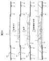
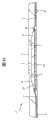
本实施例的QFN1具有利用密封体3密封了1个半导体芯片2的表面安装型的封装结构,其外形尺寸例如为长×宽=12mm×12mm,厚度=1.0mm。The QFN 1 of this embodiment has a surface-mount package structure in which one
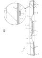
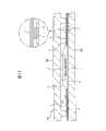
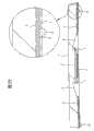
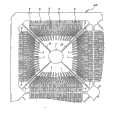
将上述的半导体芯片2在安装在金属制的管芯底座部4上的状态下配置在密封体3的中央部。该半导体芯片2的一边的尺寸例如为4mm。为了能安装例如一边的尺寸处于4mm~7mm的范围内的多种半导体芯片2,上述管芯底座部4的结构成为使其直径比半导体芯片2的直径小的所谓的小接头(tab)结构,在本实施例中,具有3mm的直径。利用与管芯底座部4形成为一体的、在密封体3的四角延伸的4条悬吊引线5b对管芯底座部4进行了支撑。The
在上述管芯底座部4的周围以包围管芯底座部4的方式配置了由与管芯底座部4和悬吊引线5b为同一金属构成的多条(例如116条)引线5。这些引线5的一个端部一侧(接近于半导体芯片2的一侧)5a经Au焊丝6与半导体芯片2的主面的键合焊盘7导电性地连接,与其相反一侧的另一个端部一侧5c以密封体3的侧面为终端。A plurality of (for example, 116) leads 5 made of the same metal as the
为了缩短与半导体芯片2的距离,使上述引线5的每一条的一个端部一侧5a分布在管芯底座部4的附近,其前端的间距(P3)为窄间距(0.18mm~0.2mm)。因此,一个端部一侧5a与邻接的引线5的间距比另一个端部一侧5c与邻接的引线5的间距小。由于通过以这种方式作成引线5的形状可缩短对引线5的一个端部一侧5a与键合焊盘7进行连线的Au焊丝6的长度(在本实施例中,为3mm以下),即使在多管脚化的情况下、或伴随多管脚化的引线5的间距、即Au焊丝6的间隔变窄的情况下,也可抑制在QFN1的制造工序(例如丝焊工序或树脂模塑工序)中Au焊丝6相互间短路的缺陷情况的发生。In order to shorten the distance with the
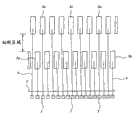
如图2中所示,在QFN1的背面(基板安装面)上设置了多个(例如116个)外部连接用端子8。沿密封体3的各边将这些端子8以锯齿状配置成各2列,各个端子8的前端部分从密封体3的背面露出,而且突出到外侧。端子8的直径(d)为0.3mm,关于与邻接的端子8的间距,与同一列的端子8的间距(P1)为0.65mm,与另一列的端子8的间距(P2)为0.325mm。As shown in FIG. 2 , a plurality of (for example, 116)
本实施例的端子8与引线5以一体的方式来形成,端子8的厚度约为125微米~150微米。此外,引线5的端子8以外的部分、即一个端部一侧5a或另一个端部一侧5c等的厚度约为65微米~75微米。此外,在突出到密封体3的外侧的端子8的前端部分上,利用电镀法或印刷法覆盖了焊剂层9。通过将这些端子8焊接到布线基板的电极(布线轨迹)上来安装本实施例的QFN1。In this embodiment, the
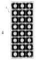
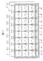
其次,说明上述QFN1的制造方法。最初,准备图6中示出的引线框LF1。该引线框LF1由Cu、Cu合金或Fe-Ni合金等的金属板构成,成为在纵和横方向上重复地形成上述的管芯底座部4、引线5、悬吊引线5b等的图形的结构。即,引线框LF1成为安装多个(例如24个)半导体芯片2的多联结构。Next, a method of manufacturing the aforementioned QFN1 will be described. Initially, lead frame LF1 shown in FIG. 6 is prepared. This lead frameLF1 is made of a metal plate such as Cu, Cu alloy, or Fe-Ni alloy, and has the pattern of the above-mentioned
为了制造上述引线框LF1,准备图7中示出的板厚约为125微米~150微米的由Cu、Cu合金或Fe-Ni合金等构成的金属板,用光致抗蚀剂膜11覆盖形成管芯底座部4、引线5和悬吊引线5b的部位的单面。此外,用光致抗蚀剂膜11覆盖形成外部连接用端子8的部位的两面。然后,在该状态下利用药液刻蚀金属板10,使单面被光致抗蚀剂膜11覆盖的区域的金属板10的板厚减薄到约一半(65微米~75微米)(半刻蚀)。通过用这样的方法进行刻蚀,两面都未被光致抗蚀剂膜11覆盖的区域的金属板10完全消失,在单面被光致抗蚀剂膜11覆盖的区域中形成厚度约为65微米~75微米的管芯底座部4、引线5和悬吊引线5b。此外,由于两面都被光致抗蚀剂膜11覆盖的区域的金属板10不被药液刻蚀,故形成具有与刻蚀前相同的厚度(125微米~150微米)的突起状的端子8。In order to manufacture the above-mentioned lead frame LF1 , prepare a metal plate made of Cu, a Cu alloy, or a Fe-Ni alloy with a thickness of about 125 μm to 150 μm shown in FIG. 7 , and cover it with a
其次,除去光致抗蚀剂膜11,接着通过对引线5的一个端部一侧5a的表面进行Ag电镀,完成上述图6中示出的引线框LF1。再有,也可对引线框LF1的整个面进行Pd(钯)电镀来代替对引线5的一个端部一侧5a进行Ag电镀的方法。由于Pd电镀与Ag电镀相比其电镀层的膜厚薄,故可提高引线5与Au焊丝6的接合性。此外,通过在引线框LF1的整个面上进行电镀,由于在端子8的表面上也同时形成电镀层,故可缩短电镀工序。Next, the
这样,通过用光致抗蚀剂膜11覆盖成为引线框LF1的母体材料的金属板10的一部分的单面来进行半刻蚀,使引线5的板厚减薄到金属板10的板厚的约一半,可高精度地加工一个端部一侧5a的间距极窄(在本实施例中,间距为0.18mm~0.2mm)的引线5。此外,通过用光致抗蚀剂膜11覆盖金属板10的一部分的两面,可与管芯底座部4、引线5和悬吊引线5b的形成同时地形成端子8。In this way, by covering one side of a part of the
其次,为了使用上述的引线框LF1来制造QFN1,首先如图8和图9中所示,使半导体芯片2的元件形成面向上地安装在管芯底座部4上,使用Au膏或环氧树脂类的粘接剂粘接这两者。Next, in order to manufacture the QFN1 using the above-mentioned lead frameLF1 , first, as shown in FIGS. A resin-based adhesive bonds the two together.
在进行上述的操作时,如图9中所示,由于突起状的端子8位于引线框LF1的背面一侧,故最好在支撑引线框LF1的夹具30A的与端子8相对的部位上形成槽31。如果这样做,则由于可稳定地支撑引线框LF1,故可防止在管芯底座部4上安装半导体芯片2时引线框LF1发生变形或管芯底座部4与半导体芯片2的位置发生偏移的缺陷情况。When performing the above-mentioned operations, as shown in FIG. 9, since the protruding
此外,本实施例的QFN1中,在将半导体芯片2安装在金属模中进行树脂模塑时,为了使半导体芯片2的上表面一侧和下表面一侧的树脂的流动变得均匀,作成通过使悬吊引线5b的一部分折弯而将管芯底座部4配置在比引线5高的位置上的接头向上的结构。因而,如图9中所示,通过在与夹具30A的管芯底座部4相对的部位上形成突起32,由于可稳定地支撑引线框LF1,故可防止在管芯底座部4上安装半导体芯片2时引线框LF1发生变形或管芯底座部4与半导体芯片2的位置发生偏移的缺陷情况。In addition, in the QFN1 of this embodiment, when mounting the
其次,如图10和图11中所示,使用众所周知的球焊装置用Au焊丝6在半导体芯片2的键合焊盘7与引线5的一个端部一侧5a之间进行连线。此时,如图11中所示,通过在支撑引线框LF1的夹具30B的与端子8相对的部位上形成槽31或在与管芯底座部4对应的部位上形成突起32,由于可稳定地支撑引线框LF1,故可防止Au焊丝6与引线5的位置偏移或Au焊丝6与键合焊盘7的位置偏移。Next, as shown in FIGS. 10 and 11 , wiring is performed between the
其次,将上述引线框LF1安装在图12中示出的金属模40中,对半导体芯片2进行树脂密封。图12是示出金属模40的一部分(约1个QFN部分的区域)的剖面图。Next, the above-mentioned lead frame LF1 is mounted in the
在使用该金属模40对半导体芯片2进行树脂密封时,首先在下模40B的表面上涂敷薄的树脂片41,在该树脂片41上放置引线框LF1。使形成了突起状端子8的面朝向下方地放置引线框LF1,使端子8与树脂片41接触。然后,在该状态下用上模40A和下模40B夹住树脂片41和引线框LF1。如果这样做,则如图中所示,由于位于引线5的下表面的端子8利用金属模40(上模40A和下模40B)的按压力来按压树脂片41,故其前端部分进入树脂片41中。When resin-sealing the
其结果,如图13中所示,通过在上模40A与下模40B的间隙(腔)中注入熔融树脂对模塑树脂进行成型来形成密封体3后,如果分离上模40A与下模40B,则进入到树脂片41中的端子8的前端部分从密封体3的背面突出到外侧。As a result, as shown in FIG. 13 , after the sealing
再有,如果用上模40A按压引线框LF1的上表面,则利用构成引线框LF1的金属板的弹力,对作为引线5的前端一侧的一个端部一侧5a作用向上的力。因此,在象本实施例的引线框LF1那样将端子8配置成2列的情况下,在接近于引线5的一个端部一侧5a处形成了端子8的引线5和在离开一个端部一侧5a处形成了端子8的引线5中在端子8按压树脂片41的力中产生差别。即,在接近于引线5的一个端部一侧5a处形成的端子8与在离开一个端部一侧5a处(=接近于上模40A与引线5的接触部分处)形成的端子8相比,按压树脂片41的力弱。其结果,接近于引线5的一个端部一侧5a处形成的端子8和在离开一个端部一侧5a处形成的端子8在从密封体3的背面突出到外侧的高度方面产生差别,在将这些端子8焊接到布线基板的电极(布线轨迹)上时,存在一部分的端子8与电极之间发生成为非接触的开路缺陷的可能性。Furthermore, when the upper surface of the lead frameLF1 is pressed by the
在存在这样的可能性的情况下,如图14中所示,最好使在接近于一个端部一侧5a处形成了端子8的引线5的宽度(W1)比在离开一个端部一侧5a处形成了端子8的引线5的宽度(W2)宽(W2<W1)。如果这样做,则由于端子8按压树脂片41的力在全部的引线5中大致相同,故进入树脂片41中的端子8的量、即从密封体3的背面突出到外侧的端子8的前端部分的高度在全部的引线5中大致相同。In the case where there is such a possibility, as shown in FIG. 14, it is preferable to make the width (W 1 ) of the
此外,如上所述,由于在本实施例中使用的引线框LF1利用半刻蚀来形成图形(管芯底座部4、引线5、悬吊引线5b),故引线5的板厚减薄到通常的引线框的约一半。因此,由于金属模40(上模40A和下模40B)按压引线框LF1的力与使用了通常的引线框的情况相比较弱,故端子8按压树脂片41的力弱的结果,突出到密封体3的外侧的高度降低。Furthermore, as described above, since the lead frameLF1 used in this embodiment is patterned (die
因此,在打算增加突出到密封体3的外侧的端子8的高度的情况下,如图15中所示,最好不对与上模40A接触的部分(用图的○标记包围的部分)的引线框LF1进行半刻蚀,使其厚度与端子8的厚度相同。Therefore, in the case where it is intended to increase the height of the
图16是用斜线示出了上述金属模40的上模40A与引线框LF1接触的部分的平面图。此外,图17是示意性地示出了该金属模40的浇口位置和在腔中注入的树脂的流动方向的平面图。FIG. 16 is a plan view showing a portion where the
如图16中所示,上述金属模40成为只是引线框LF1的外框部分和引线5与引线5的连接部分与上模40A接触、除此以外的全部的区域作为注入树脂的腔而有效地被利用的结构。As shown in FIG. 16, the
此外,如图17中所示,成为下述结构:在上述金属模40的一边上设置了多个浇口G1~G16,例如在图的左端的纵方向上并排的3个腔G1~G3中,通过浇口G1、G2中注入树脂,在与其邻接的3个腔G4~G6中,通过浇口G3、G4中注入树脂。另一方面,成为下述结构:在与上述浇口G1~G16相对的另一边上设置了虚设腔DC1~DC8和空气出口42,例如如果通过浇口G1、G2在腔C1~C3中注入树脂,则腔C1~C3内的空气流入到虚设腔DC1中,防止在腔C3内的树脂中产生空洞。In addition, as shown in FIG. 17 , it has a structure in which a plurality of gates G1 to G16 are provided on one side of the
图18是通过在上述腔C1~C18中注入树脂并对模塑树脂进行成型而对密封体3进行了成形后从金属模40取出的引线框LF1的平面图,图19是沿图18的X-X’线的剖面图,图20是引线框LF1的背面一侧的平面图。18 is a plan view of the lead frame LF1 taken out from the
其次,在引线框LF1的背面上露出的端子8的表面上形成焊剂层(9)并接着在密封体3的表面上印刷了制品名等的标记后,通过沿图18中示出的切割线切断引线框LF1和模塑树脂的一部分,完成24个在上述图1~图5中示出的本实施例的QFN1。再有,在将QFN1安装在布线基板上时,在打算增加QFN1与布线基板的间隙的情况下、即增加QFN1的基准距(standoff)的量的情况下,将在端子8的表面上形成的焊剂层9的膜厚加厚到约50微米。为了形成这样的厚的膜厚的焊剂层9,例如采用使用金属掩模在端子8的表面上印刷焊膏的方法。Next, after forming a solder layer (9) on the surface of the
这样,由于本实施例的QFN1中将引线5的一个端部一侧5a分布在管芯底座部4的附近,故可缩短一个端部一侧5a与半导体芯片2之间的距离,也可缩短连接上述部分的Au焊丝6的长度。此外,由于即使将端子8配置成锯齿状引线5的一个端部一侧5a的长度也大致相等,故一个端部一侧5a的前端相对于半导体芯片2的各边大致并排成一列。因而,可使连接引线5的一个端部一侧5a与半导体芯片2的Au焊丝6的长度大致均等,同时也可使Au焊丝6的环形状大致均等。In this way, since one
由此,由于不产生邻接的Au焊丝6相互间短路、特别是在半导体芯片2的四角附近Au焊丝6相互间交叉的缺陷情况,故提高了丝焊的操作性。此外,由于可使邻接的Au焊丝6间的间距变窄,故可实现QFN1的多管脚化。As a result, since adjacent
此外,通过使引线5的一个端部一侧5a分布在管芯底座部4的附近,从端子8到引线5的一个端部一侧5a的距离变长。由此,由于通过密封体3的外部露出的端子8侵入到密封体3的内部的水分难以到达半导体芯片2,故可防止因水分引起的键合焊盘7的腐蚀,提高了QFN1的可靠性。Furthermore, by distributing the one
此外,通过使引线5的一个端部一侧5a分布在管芯底座部4的附近,由于即使缩小半导体芯片2、Au焊丝6的长度的增加也极小(例如,即使半导体芯片2从4mm见方缩小到3mm见方,Au焊丝6的长度的增加平均也只有约0.7mm),故可防止伴随半导体芯片2的缩小的丝焊的操作性的下降。In addition, by distributing one
(实施例2)(Example 2)
在上述实施例1中,说明了使用小接头结构的引线框LF1制造的QFN,但也可例如象在图21和图22中示出的那样,使用将片状的芯片支撑体33粘贴在引线5的一个端部一侧5a上的引线框LF2来制造。在本实施例中,上述芯片支撑体33由绝缘膜构成。In the above-mentioned Embodiment 1, the QFN manufactured using the lead frameLF1 of the small joint structure was described, but it is also possible to use, for example, as shown in FIG. 21 and FIG. The lead frame LF2 is manufactured on one
可使用依据上述实施例1的引线框LF1的方法来制造本实施例中使用的引线框LF2。即,准备图23中示出的板厚约为125微米~150微米的金属板10,用光致抗蚀剂膜11覆盖形成引线5的部位的单面。此外,在形成外部连接用端子8的部位上,在两面上形成光致抗蚀剂膜11。然后,通过用在上述实施例1中说明的方法对金属板10进行半刻蚀,在同时形成了厚度约为65微米~75微米的引线5和厚度约为125微米~150微米的端子8后,在引线5的一个端部一侧5a的表面上进行Ag电镀,最后在一个端部一侧5a的上表面上粘接绝缘膜33。再有,也可利用薄的金属板那样的导电材料构成芯片支撑体33来代替绝缘膜。此时,为了防止引线5相互间的短路,使用绝缘性的粘接剂与引线5粘接即可。此外,也可利用在金属箔的表面上涂敷了绝缘性的树脂的片等来构成芯片支撑体33。The lead frame LF2 used in this embodiment can be manufactured using the method according to the lead frame LF 1of Embodiment 1 described above. That is, a
在使用上述那样的引线框LF2的情况下,通过用光致抗蚀剂膜11对金属板10的一部分的单面进行掩蔽来进行半刻蚀,由于可将引线5的板厚减薄到金属板10的约一半,故可高精度地加工引线5的一个端部一侧5a的间距极窄(例如,间距为0.18mm~0.2mm)的引线5。此外,通过用光致抗蚀剂膜11覆盖金属板10的一部分的两面,可与引线5的形成同时地形成突起状的端子8。In the case of using the lead frame LF2 as described above, half etching is performed by masking a part of one side of the
上述引线框LF2与实施例1中使用的引线框LF1不同,由于不需要支撑管芯底座部4的悬吊引线5b,故相应地可使引线5的一个端部一侧5a前端间距具有裕量。The lead frame LF2 described above is different from the lead frame LF1 used in the first embodiment, since the suspending lead 5b supporting the
此外,通过用引线5支撑芯片支撑体33,由于缩短了引线5的一个端部一侧5a与半导体芯片2的距离,故可进一步缩短Au焊丝6的长度。再者,由于与用4条悬吊引线5b来支撑管芯底座部4的情况相比能可靠地支撑芯片支撑体33,故在模塑工序中在金属模内注入熔融树脂时可抑制芯片支撑体33的移位,可防止Au焊丝6相互间的短路缺陷。Furthermore, by supporting the
如图24中所示,使用了该引线框LF2的QFN1的制造方法与在上述实施例1中已说明的方法大致相同。As shown in FIG. 24 , the method of manufacturing QFN1 using this lead frameLF2 is substantially the same as that described in the first embodiment above.
(实施例3)(Example 3)
在上述实施例1、2中,用引线框材料构成了外部连接用端子8,但也可用下述的方法来形成。In the first and second embodiments described above, the
首先,准备图25中示出的板厚约为75微米的金属板10,用光致抗蚀剂膜11覆盖形成管芯底座部4、引线5和悬吊引线5b的部位的两面。然后,通过在该状态下刻蚀金属板10,形成管芯底座部4、引线5和悬吊引线5b。其次,除去光致抗蚀剂膜11,接着,通过在引线5的一个端部一侧5a的表面上进行Ag电镀,制造引线框LF3。该引线框LF3除了没有外部连接用端子8外,成为与上述实施例1的引线框LF1相同的结构。再有,与上述实施例2的引线框LF2相同,也可用芯片支撑体33来构成管芯底座部。此外,也可通过对金属板10进行冲压来形成引线框LF3的管芯底座部4、引线5和悬吊引线5b。First, a
其次,如图26中所示,在引线框LF3的一部分上形成不被使用的虚设端子12作为实际的端子。为了形成虚设端子12,首先在将网板印刷用的掩模15重合在引线框LF3的背面上,在以后的工序中形成外部连接用的端子的部位上印刷了聚酰亚胺树脂12a后,对该聚酰亚胺树脂12a进行烘焙(图26(a)~(d))。虚设端子12的大小与在以后的工序中形成的实际端子的大小为同等程度。再有,在此,说明了通过在引线5的表面上印刷聚酰亚胺树脂12a来形成虚设端子12的情况,但不限定于此,只要能在以后的工序中从引线5的表面剥离,就不管其材料或形成方法如何。Next, as shown in FIG. 26,
其次,按照在上述实施例1中已说明的方法在管芯底座部4上安装半导体芯片2,接着用Au焊丝6连接键合焊盘7与引线5。(图26(e))。Next, the
其次,如图27(a)中所示,按照在上述实施例1中已说明的方法,通过用模塑树脂对半导体芯片2进行成形,形成密封体3。此时,在引线5的一个面上形成的上述虚设端子12的前端部分从密封体3的背面突出到外侧。Next, as shown in FIG. 27(a), the sealing
其次,如图27(b)中所示,使上述虚设端子12与引线5的一个面剥离。在用聚酰亚胺树脂构成虚设端子12的情况下,通过用肼等的有机溶剂溶解虚设端子12可进行剥离。如果剥离了虚设端子12,则在密封体3的背面上形成凹陷35,引线5的一个面露出。Next, as shown in FIG. 27(b), one surface of the
其次,如图28(a)中所示,在密封体3的背面上重合了网板印刷用的掩模16后,如图28(b)中所示,对凹陷35的内部供给焊膏13a。Next, as shown in FIG. 28(a), after the mask 16 for screen printing is superimposed on the back surface of the sealing
其次,在除去了掩模16后,在加热炉内使焊膏13a熔融。由此,如图29中所示,形成与在凹陷35的内部露出的引线5导电性地连接的、前端部分从密封体3的背面突出到外侧的焊剂凸点13。Next, after mask 16 is removed,
再有,在此,说明了通过在引线5的表面上印刷焊膏13a来形成焊剂凸点13的情况,但也可预先将成形为球状的焊剂球供给了凹陷35的内部后,通过对该焊剂球进行回流(reflow)来形成焊剂凸点13。In addition, here, the case where the
再有,通常在结束了模塑树脂的成形之后进行除去虚设端子12以形成焊剂凸点13的操作,其后切断引线框LF3将QFN1分割为各个小片,也可在将QFN1分割为各个小片后除去虚设端子12以形成焊剂凸点13。In addition, usually after the molding of the molding resin is completed, the operation of removing the
按照上述的本实施例的制造方法,与对引线框(LF1)进行半刻蚀来形成端子(8)的方法不同,可使用适合于QFN1的用途或安装基板的种类等的材料来形成端子。According to the manufacturing method of this embodiment described above, unlike the method of half-etching the lead frame (LF1 ) to form the terminal (8), the terminal can be formed using a material suitable for the application of the QFN1 or the type of mounting substrate. .
(实施例4)(Example 4)
外部连接用的端子也可用以下的方法来形成。即,如图30中所示,准备板厚约为75微米的薄的金属板20,通过用与上述实施例3同样的方法对金属板20进行刻蚀,在制造了具有管芯底座部4、引线5和在该图中未示出的悬吊引线5b的引线框LF4后,对各引线5的中间部分进行冲压成形,使其剖面形状成为锯齿状。在采用使悬吊引线5b的一部分向上方折弯的接头向上的结构的情况下,可同时进行悬吊引线5b的折弯和引线5的成形。再有,也可对在上述实施例1中使用的那样的厚的金属板10进行半刻蚀或冲压成形来形成管芯底座部4、引线5和悬吊引线5b。Terminals for external connection can also be formed by the following method. That is, as shown in FIG. 30, a thin metal plate 20 having a plate thickness of about 75 micrometers is prepared, and the metal plate 20 is etched by the same method as in the above-mentioned Example 3, and the metal plate 20 having the
其次,如图31中所示,在上述引线框LF4的管芯底座部4上安装半导体芯片2,接着在用Au焊丝6对键合焊盘7与引线5的一个端部一侧5a进行了连线后,通过用模塑树脂对半导体芯片2进行成形来形成密封体3。如果这样做,则被成形为锯齿状的引线5的凸部在密封体3的背面上露出。Next, as shown in FIG. 31, the
其次,如图32中所示,通过用研磨器等的工具研磨在密封体3的背面上露出的引线5的下端部以切断各引线5的中间部分,将1条引线5分割为多条引线5、5。Next, as shown in FIG. 32, one
其次,如图33中所示,在由1条引线5被分割的多条引线5、5上分别形成端子36。在该端子36的形成中,可使用导电性膏的印刷、焊剂球供给法或电镀法等。此外,通常在对模塑树脂进行成形以形成密封体3之后进行形成端子36的操作,其后切断引线框LF4将QFN1分割为各个小片,也可在将QFN1分割为各个小片后形成端子36。Next, as shown in FIG. 33 ,
此外,在使用上述的本实施例的端子形成方法的情况下,例如如图34中所示,在离开半导体芯片2的位置和半导体芯片2的附近处形成交替地设置了一个端部一侧5a的宽度宽的引线5、并在该引线5的各一个端部一侧5a上键合了Au焊丝后,如图35中所示,通过研磨、切断引线5的中间部分,也可分割、形成多条引线5。按照该方法,由于实质上可消除与邻接的引线5的间隔,故可大幅度地增加QFN1的端子数。Furthermore, in the case of using the terminal forming method of the present embodiment described above, for example, as shown in FIG. After the
(实施例5)(Example 5)
图36是示出在QFN的制造中使用的引线框LF5的一部分的平面图,图37是示出使用了该引线框LF5制造的QFN的内部结构(表面一侧)的平面图。36 is a plan view showing part of the lead frame LF5 used in the manufacture of the QFN, and FIG. 37 is a plan view showing the internal structure (surface side) of the QFN manufactured using the lead frame LF5 .
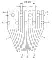
本实施例的引线框LF5成为交替地改变了包围管芯底座部4的周围的多条引线5的前端(一个端部一侧5a)的长度的结构。此外,在使用该引线框LF5的情况下,作为按照在管芯底座部4的半导体芯片2,使用沿其主面的各边将键合焊盘7以锯齿状配置成各2列的芯片。The lead frame LF5 of this embodiment has a structure in which the lengths of the ends (one
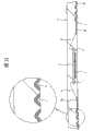
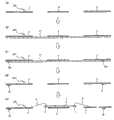
这样,在交替地改变引线框LF5的引线5的前端的长度、而且以锯齿状配置了半导体芯片2的键合焊盘7的情况下,如图38中所示,用环高度低且长度短的Au焊丝6来连接接近于半导体芯片2的外侧的列的键合焊盘7与前端的长度长的引线5,用环高度高且长度长的Au焊丝6来连接接近于半导体芯片2的外侧的列的键合焊盘7与前端的长度长的引线5。In this way, in the case where the lengths of the leading ends of the
由此,即使在伴随半导体芯片2的多管脚化引线5的间距、即Au焊丝6的间隔变窄的情况下,由于可防止互相邻接的Au焊丝6相互间的干扰,故可在QFN的制造工序(例如,丝焊工序或树脂模塑工序)中有效地抑制Au焊丝6相互间发生短路的缺陷情况的发生。Thus, even if the pitch of the
如图39中所示,上述引线框LF5也可使用于安装将键合焊盘7配置成一列的半导体芯片2的情况。此外,安装半导体芯片2的管芯底座部4的形状不限定于圆形,也可采用例如在图40中示出的引线框LF6或图41中示出的引线框LF7那样的使管芯底座部4的宽度比悬吊引线5b的宽度宽的所谓的十字形接头结构等。此时,如图40中所示,由于通过在管芯底座部4的多个部位上涂敷粘接剂14来粘接半导体芯片2,可有效地防止半导体芯片2的旋转方向的偏移,故提高了管芯底座部4与半导体芯片2的相对的位置精度。此外,由于实质上也起到悬吊引线5b的一部分的功能的管芯底座部4的宽度较宽,故也可得到提高悬吊引线5b的刚性的效果。再有,在上述那样的十字形结构的管芯底座部4中当然也可安装尺寸不同的多种半导体芯片2。As shown in FIG. 39, the lead frame LF5 described above can also be used in the case of mounting the
(实施例6)(Example 6)
也可用下述的方法来形成QFN的端子。首先,如图42(a)中所示,准备例如用上述实施例3的图25中示出的方法制造的引线框LF3。其次,如图42(b)~(d)中所示,将网板印刷用的掩模17重合在引线框LF3的背面上,在形成端子的部位上印刷了Cu膏18a后,通过对该Cu膏18a进行烘焙,形成Cu端子18。The terminals of the QFN can also be formed by the following method. First, as shown in FIG. 42(a), a
其次,如图42(e)中所示,按照上述实施例1中已说明的方法在管芯底座部4上安装半导体芯片2,接着用Au焊丝6连接键合焊盘7与引线5。Next, as shown in FIG. 42(e), the
其次,如图43中所示,按照上述实施例1中已说明的方法,通过用模塑树脂对半导体芯片2进行成形来形成密封体3。由此,在引线5的一个面上形成的上述Cu端子18的前端部分从密封体3的背面突出到外侧。Next, as shown in FIG. 43, the sealing
其后,也可根据需要使用无电解电镀法对Cu端子18的表面进行Sn或Au的电镀。Thereafter, the surface of the
按照上述的本实施例的制造方法,与在引线5的一个面上形成了虚设端子12后除去虚设端子12以形成焊剂凸点13的上述实施例3的方法相比,可简化端子形成工序。According to the manufacturing method of the present embodiment described above, the terminal forming process can be simplified compared with the method of the third embodiment in which the
(实施例7)(Example 7)
图44中示出的QFN1是将引线5的一个端部一侧(接近于半导体芯片2的一侧)5a向上方折弯的例子。如果这样做,则由于可减小引线5的一个端部一侧5a与半导体芯片2的主面的台阶差,可降低连接引线5与键合焊盘7的Au焊丝6的环高度,故相应地可减薄密封体3的厚度。The QFN1 shown in FIG. 44 is an example in which one end side (the side closer to the semiconductor chip 2 ) 5 a of the
此外,图45中示出的QFN1是在使引线5的一个端部一侧5a向上方折弯的同时使管芯底座部4的高度与引线5的一个端部一侧5a高度大致相同、以倒装方式在管芯底座部4的下表面一侧安装半导体芯片2的例子。如果这样做,则由于可使引线5的一个端部一侧5a和管芯底座部4的各自的上表面与密封体3的上表面之间的树脂厚度非常薄,故可实现密封体3的厚度约为0.5mm的超薄型QFN。In addition, QFN1 shown in FIG. An example in which the
使引线5的一个端部一侧5a向上方折弯的上述方式,例如如图46和图47中所示,也可应用于使用将由绝缘膜构成的芯片支撑体33粘贴到引线5的一个端部一侧5a上的引线框LF2的情况。例如经在芯片支撑体33的单面上形成的粘接剂19来进行芯片支撑体33与半导体芯片2的粘接。此时,根据上述的原因,也可减薄密封体3的厚度。The above-described method of bending one
图48和图49是使用例如由Cu或Al那样的热传导性高的材料构成的散热器23构成芯片支撑体的例子。通过将散热器23兼用作芯片支撑体,可实现散热性良好的QFN。此外,在使用散热器23构成芯片支撑体的情况下,如图50中所示,也可使散热器23的一个面在密封体3的表面上露出,由此,可进一步提高散热性。FIGS. 48 and 49 are examples in which a chip support is formed using a
再有,本实施例应用于具有对引线框进行半刻蚀而形成的端子8的QFN,但不限定于此,当然也可应用于具有用上述的各种方法形成的端子的QFN。In addition, this embodiment is applied to a
(实施例8)(Embodiment 8)
图51是示出在QFN的制造中使用的引线框LF8的一部分的平面图,图52是示出使用该引线框LF8制造的QFN的外观(背面一侧)的平面图。FIG. 51 is a plan view showing part of the lead frame LF8 used in the manufacture of the QFN, and FIG. 52 is a plan view showing the appearance (back side) of the QFN manufactured using the lead frame LF8 .
在QFN的封装尺寸为恒定的状态下推行多管脚化的情况下,由于端子8的间距极窄,故如在上述实施例1中使用的引线框LF1那样,如果打算使端子8的宽度比引线5的宽度宽,则引线框的加工是非常困难的。When multiple pins are promoted while the package size of QFN is constant, the pitch of terminals8 is extremely narrow. If it is wider than the width of the
作为其对策,如本实施例的引线框LF8那样,希望端子8的宽度与引线5的宽度相同。由此,可实现下述的窄间距超多管脚的QFN:例如,端子8和引线5的宽度(d)为0.15~0.18mm,关于与邻接的端子8的间距,与同一列的端子8的间距(P1)为0.5mm,与其它列的端子的间距(P2)为0.25mm。As a countermeasure against this, it is desirable that the width of the terminal8 be the same as that of the
此时,由于通过使端子8的宽度变窄端子8与安装基板的接触面积减小,连接可靠性下降,故作为补偿这一点的方法,希望通过加长端子8的长度来防止面积的下降。此外,由于因引线5的宽度变窄引线5的强度也下降,故希望通过在引线5的前端粘贴芯片支撑体33、用该芯片支撑体33支撑引线5来防止引线5的变形。如图53中所示,也可在引线5的中间部分设置芯片支撑体33。如图54和图55中所示,当然也可将使端子8的宽度与引线5的宽度相同的本实施例的引线框LF8应用于没有芯片支撑体33的引线框。At this time, since the contact area between the terminal 8 and the mounting substrate is reduced by narrowing the width of the
以上根据发明的实施例具体地说明了由本发明者进行的发明,但本发明不限定于上述发明的实施例,在不脱离其要旨的范围内,当然可作各种变更。As mentioned above, the invention made by this inventor was concretely demonstrated based on the Example of this invention, However, this invention is not limited to the said Example of invention, Of course, various changes are possible in the range which does not deviate from the summary.
例如,在使用上述实施例1中已说明的金属模40同时对安装在一个引线框LF1上的多个半导体芯片2进行树脂密封的情况下,有时起因于引线框LF1与模塑设置的热膨胀系数的差,在切割前的引线框LF1中产生翘曲或变形。For example, in the case of simultaneously resin-sealing a plurality of
为了防止这一点,例如如图56中所示,在引线框LF1的外框部分上设置缝隙22是有效的。此外,通过改变构成密封体3的模塑树脂中包含的填充剂等的量、使密封体3的热膨胀系数接近于引线框LF1的热膨胀系数也是有效的。In order to prevent this, for example, as shown in FIG. 56, it is effective to provide a
此外,例如如图57中所示,通过使管芯底座部4在密封体3的背面上露出,可实现散热性高的QFN1。为了在密封体3的背面上使管芯底座部4露出,例如在对厚的板厚的金属板10进行半刻蚀来形成薄的板厚的引线5和悬吊引线5b时,通过用光致抗蚀剂膜覆盖管芯底座部4,可形成厚的板厚的管芯底座部4。In addition, as shown in FIG. 57, for example, by exposing the
此外,在上述实施例1中,对厚的板厚的金属板10进行半刻蚀形成了薄的板厚的管芯底座部4、引线5和悬吊引线5b,但在薄的板厚的悬吊引线5b上安装了较大尺寸的半导体芯片2的情况下,有时悬吊引线5b的刚性不够。作为其对策,例如如图58中所示,不对悬吊引线5b的一部分或整体进行半刻蚀,用厚的板厚来形成悬吊引线5b,这样做是有效的。此外,此时,由于悬吊引线5b的一部分(或整体)从密封体3的背面露出,故通过将该露出部分焊接到布线基板上,可提高QFN1与布线基板的连接可靠性及QFN1的散热性。In addition, in the first embodiment described above, the
此外,在上述实施例中,在形成密封体3时,使用了在金属模40(上模40A与下模40B)之间夹住树脂片41的模塑成形方法,但也可如图59中所示,用不使用树脂片41的模塑成形方法来形成密封体3。此时,在从金属模40中取出密封体3时,如图60(a)中所示,端子8的一部分被树脂覆盖,或如图60(b)中所示,有时端子8的整体被树脂覆盖,因此,如图61中所示,使用研磨器等的毛刺除去装置37来除去端子8的表面的树脂毛刺,其后,用上述的印刷法或电镀法在端子8的表面上形成金属层即可。In addition, in the above-mentioned embodiment, when forming the sealing
Claims (10)
Applications Claiming Priority (4)
| Application Number | Priority Date | Filing Date | Title |
|---|---|---|---|
| JP381427/2001 | 2001-12-14 | ||
| JP2001381427 | 2001-12-14 | ||
| JP291975/2002 | 2002-10-04 | ||
| JP2002291975AJP4173346B2 (en) | 2001-12-14 | 2002-10-04 | Semiconductor device |
Related Parent Applications (1)
| Application Number | Title | Priority Date | Filing Date |
|---|---|---|---|
| CN02151384ADivisionCN1424757A (en) | 2001-12-14 | 2002-11-20 | Semiconductor device and manufacturing method thereof |
Publications (2)
| Publication Number | Publication Date |
|---|---|
| CN101447438A CN101447438A (en) | 2009-06-03 |
| CN101447438Btrue CN101447438B (en) | 2010-12-01 |
Family
ID=38943358
Family Applications (2)
| Application Number | Title | Priority Date | Filing Date |
|---|---|---|---|
| CN2008101863830AExpired - Fee RelatedCN101447438B (en) | 2001-12-14 | 2002-11-20 | Manufacturing method of semiconductor device |
| CNB2007101120301AExpired - Fee RelatedCN100536121C (en) | 2001-12-14 | 2002-11-20 | Semiconductor device and preparation method thereof |
Family Applications After (1)
| Application Number | Title | Priority Date | Filing Date |
|---|---|---|---|
| CNB2007101120301AExpired - Fee RelatedCN100536121C (en) | 2001-12-14 | 2002-11-20 | Semiconductor device and preparation method thereof |
Country Status (2)
| Country | Link |
|---|---|
| JP (2) | JP4747188B2 (en) |
| CN (2) | CN101447438B (en) |
Families Citing this family (1)
| Publication number | Priority date | Publication date | Assignee | Title |
|---|---|---|---|---|
| JP6121692B2 (en)* | 2012-11-05 | 2017-04-26 | ルネサスエレクトロニクス株式会社 | Semiconductor device and manufacturing method thereof |
Citations (1)
| Publication number | Priority date | Publication date | Assignee | Title |
|---|---|---|---|---|
| CN1242104A (en)* | 1996-11-28 | 2000-01-19 | 株式会社尼康 | Exposure device and exposure method |
Family Cites Families (11)
| Publication number | Priority date | Publication date | Assignee | Title |
|---|---|---|---|---|
| JP3227792B2 (en)* | 1992-05-18 | 2001-11-12 | ソニー株式会社 | Resin sealing method for semiconductor device |
| US5637914A (en)* | 1994-05-16 | 1997-06-10 | Hitachi, Ltd. | Lead frame and semiconductor device encapsulated by resin |
| JPH0878605A (en)* | 1994-09-01 | 1996-03-22 | Hitachi Ltd | Lead frame and semiconductor integrated circuit device using the same |
| CN1143371C (en)* | 1996-12-26 | 2004-03-24 | 株式会社日立制作所 | Molded plastic type semiconductor device and its manufacturing process |
| JP3493113B2 (en)* | 1997-03-21 | 2004-02-03 | 株式会社ルネサステクノロジ | Semiconductor device manufacturing method and lead frame |
| JP2000091488A (en)* | 1998-09-08 | 2000-03-31 | Dainippon Printing Co Ltd | Resin-sealed semiconductor device and circuit member used for the same |
| JP3455116B2 (en)* | 1998-09-30 | 2003-10-14 | 株式会社三井ハイテック | Method for manufacturing semiconductor device |
| JP3959898B2 (en)* | 1999-09-01 | 2007-08-15 | 松下電器産業株式会社 | Manufacturing method of resin-encapsulated semiconductor device |
| JP2001077287A (en)* | 1999-09-06 | 2001-03-23 | Mitsubishi Electric Corp | Lead frame for semiconductor device |
| JP3751496B2 (en)* | 2000-03-02 | 2006-03-01 | 松下電器産業株式会社 | Lead frame and method for manufacturing resin-encapsulated semiconductor device using the same |
| JP4173346B2 (en)* | 2001-12-14 | 2008-10-29 | 株式会社ルネサステクノロジ | Semiconductor device |
- 2002
- 2002-11-20CNCN2008101863830Apatent/CN101447438B/ennot_activeExpired - Fee Related
- 2002-11-20CNCNB2007101120301Apatent/CN100536121C/ennot_activeExpired - Fee Related
- 2008
- 2008-06-16JPJP2008156464Apatent/JP4747188B2/ennot_activeExpired - Fee Related
- 2011
- 2011-04-04JPJP2011082422Apatent/JP2011155293A/enactivePending
Patent Citations (1)
| Publication number | Priority date | Publication date | Assignee | Title |
|---|---|---|---|---|
| CN1242104A (en)* | 1996-11-28 | 2000-01-19 | 株式会社尼康 | Exposure device and exposure method |
Non-Patent Citations (1)
| Title |
|---|
| JP平8-139259A 1996.05.31 |
Also Published As
| Publication number | Publication date |
|---|---|
| CN101090102A (en) | 2007-12-19 |
| JP2011155293A (en) | 2011-08-11 |
| JP4747188B2 (en) | 2011-08-17 |
| JP2008258652A (en) | 2008-10-23 |
| CN101447438A (en) | 2009-06-03 |
| CN100536121C (en) | 2009-09-02 |
Similar Documents
| Publication | Publication Date | Title |
|---|---|---|
| JP4173346B2 (en) | Semiconductor device | |
| JP3062192B1 (en) | Lead frame and method of manufacturing resin-encapsulated semiconductor device using the same | |
| US6084292A (en) | Lead frame and semiconductor device using the lead frame | |
| JP4095827B2 (en) | Semiconductor device | |
| KR20040030297A (en) | Lead frame, method of manufacturing the same, and semiconductor device manufactured with the same | |
| JP2004214233A (en) | Semiconductor device and manufacturing method therefor | |
| US6780679B2 (en) | Semiconductor device and method of manufacturing the same | |
| US6642082B2 (en) | Method for manufacturing a resin-sealed semiconductor device | |
| US20050189627A1 (en) | Method of surface mounting a semiconductor device | |
| JP2004363365A (en) | Semiconductor device and manufacturing method thereof | |
| JP2011142337A (en) | Method of manufacturing semiconductor device | |
| CN101325191A (en) | Square flat pin-free packaging structure with patterns on chip | |
| JP2001024133A (en) | Lead frame, resin sealed semiconductor device employing it and manufacture thereof | |
| JP4243270B2 (en) | Manufacturing method of semiconductor device | |
| CN101447438B (en) | Manufacturing method of semiconductor device | |
| JP2001077285A (en) | Lead frame and manufacture of resin-sealed semiconductor device using the same | |
| JP2001077275A (en) | Lead frame and manufacture of resin-sealed semiconductor device using the same | |
| KR100246848B1 (en) | Land grid array and a semiconductor package having a same | |
| JPH0834282B2 (en) | Lead frame for semiconductor device | |
| JP2001077136A (en) | Manufacture of plastic molded semiconductor device | |
| JP2000150707A (en) | Resin-sealed semiconductor device and manufacture thereof | |
| JP2006216979A (en) | Manufacturing method for semiconductor device | |
| JPH10199899A (en) | Manufacture of semiconductor device | |
| JP2003007953A (en) | Resin-sealed semiconductor device and method of manufacturing the same | |
| JP2001077273A (en) | Lead frame and manufacture of resin-sealed semiconductor device using the same |
Legal Events
| Date | Code | Title | Description |
|---|---|---|---|
| C06 | Publication | ||
| PB01 | Publication | ||
| C10 | Entry into substantive examination | ||
| SE01 | Entry into force of request for substantive examination | ||
| ASS | Succession or assignment of patent right | Owner name:NEC CORP Free format text:FORMER OWNER: RENESAS TECHNOLOGY CO., LTD Effective date:20100712 | |
| C41 | Transfer of patent application or patent right or utility model | ||
| COR | Change of bibliographic data | Free format text:CORRECT: ADDRESS; FROM: TOKYO, JAPAN TO: KANAGAWA, JAPAN | |
| TA01 | Transfer of patent application right | Effective date of registration:20100712 Address after:Kanagawa, Japan Applicant after:NEC Corp. Address before:Tokyo, Japan Applicant before:Renesas Technology Corp. | |
| C14 | Grant of patent or utility model | ||
| GR01 | Patent grant | ||
| C17 | Cessation of patent right | ||
| CF01 | Termination of patent right due to non-payment of annual fee | Granted publication date:20101201 Termination date:20131120 |