CN101442106A - Semiconductor device, method for manufacturing the same, liquid crystal television, and el television - Google Patents
Semiconductor device, method for manufacturing the same, liquid crystal television, and el televisionDownload PDFInfo
- Publication number
- CN101442106A CN101442106ACNA2008101852751ACN200810185275ACN101442106ACN 101442106 ACN101442106 ACN 101442106ACN A2008101852751 ACNA2008101852751 ACN A2008101852751ACN 200810185275 ACN200810185275 ACN 200810185275ACN 101442106 ACN101442106 ACN 101442106A
- Authority
- CN
- China
- Prior art keywords
- conductive layer
- insulating barrier
- semiconductor device
- semiconductor
- thickness
- Prior art date
- Legal status (The legal status is an assumption and is not a legal conclusion. Google has not performed a legal analysis and makes no representation as to the accuracy of the status listed.)
- Granted
Links
- 239000004065semiconductorSubstances0.000titleclaimsabstractdescription271
- 238000000034methodMethods0.000titleclaimsabstractdescription146
- 238000004519manufacturing processMethods0.000titleclaimsabstractdescription81
- 239000004973liquid crystal related substanceSubstances0.000titleabstractdescription42
- 239000000758substrateSubstances0.000claimsabstractdescription125
- 230000004888barrier functionEffects0.000claimsdescription46
- 238000005507sprayingMethods0.000claimsdescription29
- 238000000576coating methodMethods0.000claimsdescription20
- 239000011248coating agentSubstances0.000claimsdescription18
- 239000011810insulating materialSubstances0.000claimsdescription12
- 238000004528spin coatingMethods0.000claimsdescription12
- 238000005268plasma chemical vapour depositionMethods0.000claimsdescription9
- 238000007639printingMethods0.000claimsdescription8
- 238000005229chemical vapour depositionMethods0.000claimsdescription6
- 238000005240physical vapour depositionMethods0.000claimsdescription6
- 238000007747platingMethods0.000claimsdescription4
- 239000000463materialSubstances0.000abstractdescription122
- 230000008569processEffects0.000abstractdescription56
- 238000009413insulationMethods0.000abstract1
- 239000010410layerSubstances0.000description472
- 239000010408filmSubstances0.000description237
- -1polyethylene naphthalatePolymers0.000description50
- 239000000243solutionSubstances0.000description46
- 239000007788liquidSubstances0.000description42
- 229920005989resinPolymers0.000description41
- 239000011347resinSubstances0.000description41
- 239000000203mixtureSubstances0.000description36
- 239000000126substanceSubstances0.000description33
- 239000011159matrix materialSubstances0.000description31
- VYPSYNLAJGMNEJ-UHFFFAOYSA-Nsilicon dioxideInorganic materialsO=[Si]=OVYPSYNLAJGMNEJ-UHFFFAOYSA-N0.000description25
- 229910052710siliconInorganic materials0.000description24
- 238000005530etchingMethods0.000description23
- 238000002347injectionMethods0.000description23
- 239000007924injectionSubstances0.000description23
- XUIMIQQOPSSXEZ-UHFFFAOYSA-NSiliconChemical compound[Si]XUIMIQQOPSSXEZ-UHFFFAOYSA-N0.000description22
- 239000007789gasSubstances0.000description22
- 239000010703siliconSubstances0.000description22
- 229910052814silicon oxideInorganic materials0.000description22
- 239000004020conductorSubstances0.000description21
- 230000001681protective effectEffects0.000description21
- 239000002245particleSubstances0.000description19
- 239000002904solventSubstances0.000description19
- 229920001721polyimidePolymers0.000description18
- 239000004642PolyimideSubstances0.000description17
- 239000011521glassSubstances0.000description17
- 238000010438heat treatmentMethods0.000description17
- 229910052751metalInorganic materials0.000description17
- 229910052760oxygenInorganic materials0.000description17
- 229910052782aluminiumInorganic materials0.000description16
- QVGXLLKOCUKJST-UHFFFAOYSA-Natomic oxygenChemical compound[O]QVGXLLKOCUKJST-UHFFFAOYSA-N0.000description16
- 230000015572biosynthetic processEffects0.000description16
- 239000002184metalSubstances0.000description16
- 239000001301oxygenSubstances0.000description16
- IJGRMHOSHXDMSA-UHFFFAOYSA-NAtomic nitrogenChemical compoundN#NIJGRMHOSHXDMSA-UHFFFAOYSA-N0.000description15
- XAGFODPZIPBFFR-UHFFFAOYSA-NaluminiumChemical compound[Al]XAGFODPZIPBFFR-UHFFFAOYSA-N0.000description15
- 230000006870functionEffects0.000description15
- 229910052709silverInorganic materials0.000description14
- LFQSCWFLJHTTHZ-UHFFFAOYSA-NEthanolChemical compoundCCOLFQSCWFLJHTTHZ-UHFFFAOYSA-N0.000description13
- 239000004332silverSubstances0.000description13
- BQCADISMDOOEFD-UHFFFAOYSA-NSilverChemical compound[Ag]BQCADISMDOOEFD-UHFFFAOYSA-N0.000description12
- 239000002274desiccantSubstances0.000description12
- 238000001035dryingMethods0.000description12
- 239000011229interlayerSubstances0.000description12
- 239000000565sealantSubstances0.000description12
- 239000010409thin filmSubstances0.000description12
- 229910052581Si3N4Inorganic materials0.000description11
- XLOMVQKBTHCTTD-UHFFFAOYSA-NZinc monoxideChemical compound[Zn]=OXLOMVQKBTHCTTD-UHFFFAOYSA-N0.000description11
- 238000005520cutting processMethods0.000description11
- PQXKHYXIUOZZFA-UHFFFAOYSA-Mlithium fluorideChemical compound[Li+].[F-]PQXKHYXIUOZZFA-UHFFFAOYSA-M0.000description11
- HQVNEWCFYHHQES-UHFFFAOYSA-Nsilicon nitrideChemical compoundN12[Si]34N5[Si]62N3[Si]51N64HQVNEWCFYHHQES-UHFFFAOYSA-N0.000description11
- 239000000853adhesiveSubstances0.000description10
- 230000001070adhesive effectEffects0.000description10
- 239000003990capacitorSubstances0.000description10
- 230000005525hole transportEffects0.000description10
- 239000007769metal materialSubstances0.000description10
- 229910052757nitrogenInorganic materials0.000description10
- ZMXDDKWLCZADIW-UHFFFAOYSA-NN,N-DimethylformamideChemical compoundCN(C)C=OZMXDDKWLCZADIW-UHFFFAOYSA-N0.000description9
- 229910052784alkaline earth metalInorganic materials0.000description9
- 239000010949copperSubstances0.000description9
- 238000010586diagramMethods0.000description9
- 239000003822epoxy resinSubstances0.000description9
- 239000010931goldSubstances0.000description9
- 239000012212insulatorSubstances0.000description9
- BASFCYQUMIYNBI-UHFFFAOYSA-NplatinumSubstances[Pt]BASFCYQUMIYNBI-UHFFFAOYSA-N0.000description9
- 229920000647polyepoxidePolymers0.000description9
- 150000001342alkaline earth metalsChemical class0.000description8
- 238000004380ashingMethods0.000description8
- 229910052802copperInorganic materials0.000description8
- AMGQUBHHOARCQH-UHFFFAOYSA-Nindium;oxotinChemical compound[In].[Sn]=OAMGQUBHHOARCQH-UHFFFAOYSA-N0.000description8
- 238000000206photolithographyMethods0.000description8
- UHOVQNZJYSORNB-UHFFFAOYSA-NBenzeneChemical groupC1=CC=CC=C1UHOVQNZJYSORNB-UHFFFAOYSA-N0.000description7
- RYGMFSIKBFXOCR-UHFFFAOYSA-NCopperChemical compound[Cu]RYGMFSIKBFXOCR-UHFFFAOYSA-N0.000description7
- 239000010419fine particleSubstances0.000description7
- 229910052737goldInorganic materials0.000description7
- KDLHZDBZIXYQEI-UHFFFAOYSA-NpalladiumSubstances[Pd]KDLHZDBZIXYQEI-UHFFFAOYSA-N0.000description7
- XKRFYHLGVUSROY-UHFFFAOYSA-NArgonChemical compound[Ar]XKRFYHLGVUSROY-UHFFFAOYSA-N0.000description6
- YMWUJEATGCHHMB-UHFFFAOYSA-NDichloromethaneChemical compoundClCClYMWUJEATGCHHMB-UHFFFAOYSA-N0.000description6
- WYURNTSHIVDZCO-UHFFFAOYSA-NTetrahydrofuranChemical compoundC1CCOC1WYURNTSHIVDZCO-UHFFFAOYSA-N0.000description6
- YXFVVABEGXRONW-UHFFFAOYSA-NTolueneChemical compoundCC1=CC=CC=C1YXFVVABEGXRONW-UHFFFAOYSA-N0.000description6
- 230000015556catabolic processEffects0.000description6
- 150000001875compoundsChemical class0.000description6
- 238000001514detection methodMethods0.000description6
- PCHJSUWPFVWCPO-UHFFFAOYSA-NgoldChemical compound[Au]PCHJSUWPFVWCPO-UHFFFAOYSA-N0.000description6
- 150000002894organic compoundsChemical class0.000description6
- 229920000642polymerPolymers0.000description6
- 239000002861polymer materialSubstances0.000description6
- 229920000123polythiophenePolymers0.000description6
- XLYOFNOQVPJJNP-UHFFFAOYSA-NwaterSubstancesOXLYOFNOQVPJJNP-UHFFFAOYSA-N0.000description6
- RTZKZFJDLAIYFH-UHFFFAOYSA-NDiethyl etherChemical compoundCCOCCRTZKZFJDLAIYFH-UHFFFAOYSA-N0.000description5
- SECXISVLQFMRJM-UHFFFAOYSA-NN-MethylpyrrolidoneChemical compoundCN1CCCC1=OSECXISVLQFMRJM-UHFFFAOYSA-N0.000description5
- 229920001609Poly(3,4-ethylenedioxythiophene)Polymers0.000description5
- 239000006087Silane Coupling AgentSubstances0.000description5
- NIXOWILDQLNWCW-UHFFFAOYSA-Nacrylic acid groupChemical groupC(C=C)(=O)ONIXOWILDQLNWCW-UHFFFAOYSA-N0.000description5
- 229910052783alkali metalInorganic materials0.000description5
- 150000001340alkali metalsChemical class0.000description5
- IISBACLAFKSPIT-UHFFFAOYSA-Nbisphenol AChemical compoundC=1C=C(O)C=CC=1C(C)(C)C1=CC=C(O)C=C1IISBACLAFKSPIT-UHFFFAOYSA-N0.000description5
- 239000005380borophosphosilicate glassSubstances0.000description5
- 239000000872bufferSubstances0.000description5
- 239000013078crystalSubstances0.000description5
- 230000001747exhibiting effectEffects0.000description5
- 238000011049fillingMethods0.000description5
- 239000001257hydrogenSubstances0.000description5
- 229910052739hydrogenInorganic materials0.000description5
- 230000000737periodic effectEffects0.000description5
- 229910052697platinumInorganic materials0.000description5
- 229920001467poly(styrenesulfonates)Polymers0.000description5
- 229910021332silicideInorganic materials0.000description5
- FVBUAEGBCNSCDD-UHFFFAOYSA-Nsilicide(4-)Chemical compound[Si-4]FVBUAEGBCNSCDD-UHFFFAOYSA-N0.000description5
- 238000004544sputter depositionMethods0.000description5
- 238000002834transmittanceMethods0.000description5
- ZWEHNKRNPOVVGH-UHFFFAOYSA-N2-ButanoneChemical compoundCCC(C)=OZWEHNKRNPOVVGH-UHFFFAOYSA-N0.000description4
- 239000004925Acrylic resinSubstances0.000description4
- 229920000178Acrylic resinPolymers0.000description4
- HEDRZPFGACZZDS-UHFFFAOYSA-NChloroformChemical compoundClC(Cl)ClHEDRZPFGACZZDS-UHFFFAOYSA-N0.000description4
- KRHYYFGTRYWZRS-UHFFFAOYSA-MFluoride anionChemical compound[F-]KRHYYFGTRYWZRS-UHFFFAOYSA-M0.000description4
- UFHFLCQGNIYNRP-UHFFFAOYSA-NHydrogenChemical compound[H][H]UFHFLCQGNIYNRP-UHFFFAOYSA-N0.000description4
- OAICVXFJPJFONN-UHFFFAOYSA-NPhosphorusChemical compound[P]OAICVXFJPJFONN-UHFFFAOYSA-N0.000description4
- 229920000265PolyparaphenylenePolymers0.000description4
- 239000000956alloySubstances0.000description4
- 239000012298atmosphereSubstances0.000description4
- XJHCXCQVJFPJIK-UHFFFAOYSA-Mcaesium fluorideChemical compound[F-].[Cs+]XJHCXCQVJFPJIK-UHFFFAOYSA-M0.000description4
- 238000006731degradation reactionMethods0.000description4
- 239000003989dielectric materialSubstances0.000description4
- KPUWHANPEXNPJT-UHFFFAOYSA-NdisiloxaneChemical class[SiH3]O[SiH3]KPUWHANPEXNPJT-UHFFFAOYSA-N0.000description4
- 238000005516engineering processMethods0.000description4
- 229910010272inorganic materialInorganic materials0.000description4
- 238000010030laminatingMethods0.000description4
- 239000002105nanoparticleSubstances0.000description4
- 229910052763palladiumInorganic materials0.000description4
- 230000035699permeabilityEffects0.000description4
- 229910052698phosphorusInorganic materials0.000description4
- 239000011574phosphorusSubstances0.000description4
- 229920002120photoresistant polymerPolymers0.000description4
- 229920003227poly(N-vinyl carbazole)Polymers0.000description4
- 229920002098polyfluorenePolymers0.000description4
- 229960002796polystyrene sulfonateDrugs0.000description4
- 239000011970polystyrene sulfonateSubstances0.000description4
- 229910052719titaniumInorganic materials0.000description4
- 239000010936titaniumSubstances0.000description4
- TVIVIEFSHFOWTE-UHFFFAOYSA-Ktri(quinolin-8-yloxy)alumaneChemical compound[Al+3].C1=CN=C2C([O-])=CC=CC2=C1.C1=CN=C2C([O-])=CC=CC2=C1.C1=CN=C2C([O-])=CC=CC2=C1TVIVIEFSHFOWTE-UHFFFAOYSA-K0.000description4
- 229910052721tungstenInorganic materials0.000description4
- 238000007740vapor depositionMethods0.000description4
- 125000000391vinyl groupChemical group[H]C([*])=C([H])[H]0.000description4
- 239000011787zinc oxideSubstances0.000description4
- QTBSBXVTEAMEQO-UHFFFAOYSA-NAcetic acidChemical compoundCC(O)=OQTBSBXVTEAMEQO-UHFFFAOYSA-N0.000description3
- CSCPPACGZOOCGX-UHFFFAOYSA-NAcetoneChemical compoundCC(C)=OCSCPPACGZOOCGX-UHFFFAOYSA-N0.000description3
- NIXOWILDQLNWCW-UHFFFAOYSA-MAcrylateChemical compound[O-]C(=O)C=CNIXOWILDQLNWCW-UHFFFAOYSA-M0.000description3
- XEKOWRVHYACXOJ-UHFFFAOYSA-NEthyl acetateChemical compoundCCOC(C)=OXEKOWRVHYACXOJ-UHFFFAOYSA-N0.000description3
- IMNFDUFMRHMDMM-UHFFFAOYSA-NN-HeptaneChemical compoundCCCCCCCIMNFDUFMRHMDMM-UHFFFAOYSA-N0.000description3
- 239000004952PolyamideSubstances0.000description3
- 239000004372Polyvinyl alcoholSubstances0.000description3
- 229910045601alloyInorganic materials0.000description3
- HSFWRNGVRCDJHI-UHFFFAOYSA-Nalpha-acetyleneNatural productsC#CHSFWRNGVRCDJHI-UHFFFAOYSA-N0.000description3
- 229910021417amorphous siliconInorganic materials0.000description3
- 229910052786argonInorganic materials0.000description3
- 150000004696coordination complexChemical class0.000description3
- VBVAVBCYMYWNOU-UHFFFAOYSA-Ncoumarin 6Chemical compoundC1=CC=C2SC(C3=CC4=CC=C(C=C4OC3=O)N(CC)CC)=NC2=C1VBVAVBCYMYWNOU-UHFFFAOYSA-N0.000description3
- 125000004122cyclic groupChemical group0.000description3
- 238000001312dry etchingMethods0.000description3
- 238000001704evaporationMethods0.000description3
- LNEPOXFFQSENCJ-UHFFFAOYSA-NhaloperidolChemical compoundC1CC(O)(C=2C=CC(Cl)=CC=2)CCN1CCCC(=O)C1=CC=C(F)C=C1LNEPOXFFQSENCJ-UHFFFAOYSA-N0.000description3
- 229910052738indiumInorganic materials0.000description3
- APFVFJFRJDLVQX-UHFFFAOYSA-Nindium atomChemical compound[In]APFVFJFRJDLVQX-UHFFFAOYSA-N0.000description3
- 230000015654memoryEffects0.000description3
- 150000002739metalsChemical class0.000description3
- 238000002156mixingMethods0.000description3
- 230000004048modificationEffects0.000description3
- 238000012986modificationMethods0.000description3
- 229910000476molybdenum oxideInorganic materials0.000description3
- PXHVJJICTQNCMI-UHFFFAOYSA-NnickelSubstances[Ni]PXHVJJICTQNCMI-UHFFFAOYSA-N0.000description3
- 239000003960organic solventSubstances0.000description3
- TWNQGVIAIRXVLR-UHFFFAOYSA-Noxo(oxoalumanyloxy)alumaneChemical compoundO=[Al]O[Al]=OTWNQGVIAIRXVLR-UHFFFAOYSA-N0.000description3
- 230000000149penetrating effectEffects0.000description3
- 230000002093peripheral effectEffects0.000description3
- 239000000049pigmentSubstances0.000description3
- 238000009832plasma treatmentMethods0.000description3
- 229920003023plasticPolymers0.000description3
- 239000004033plasticSubstances0.000description3
- 229920001197polyacetylenePolymers0.000description3
- 229920002647polyamidePolymers0.000description3
- 229920000767polyanilinePolymers0.000description3
- 229920006393polyether sulfonePolymers0.000description3
- 229920001709polysilazanePolymers0.000description3
- 229920002451polyvinyl alcoholPolymers0.000description3
- 239000002243precursorSubstances0.000description3
- 239000011241protective layerSubstances0.000description3
- 238000007789sealingMethods0.000description3
- 238000001179sorption measurementMethods0.000description3
- 239000007921spraySubstances0.000description3
- YLQBMQCUIZJEEH-UHFFFAOYSA-NtetrahydrofuranNatural productsC=1C=COC=1YLQBMQCUIZJEEH-UHFFFAOYSA-N0.000description3
- CXWXQJXEFPUFDZ-UHFFFAOYSA-NtetralinChemical compoundC1=CC=C2CCCCC2=C1CXWXQJXEFPUFDZ-UHFFFAOYSA-N0.000description3
- WFKWXMTUELFFGS-UHFFFAOYSA-NtungstenChemical compound[W]WFKWXMTUELFFGS-UHFFFAOYSA-N0.000description3
- 239000010937tungstenSubstances0.000description3
- 229910001935vanadium oxideInorganic materials0.000description3
- 229920002554vinyl polymerPolymers0.000description3
- 235000012431wafersNutrition0.000description3
- YVTHLONGBIQYBO-UHFFFAOYSA-Nzinc indium(3+) oxygen(2-)Chemical compound[O--].[Zn++].[In+3]YVTHLONGBIQYBO-UHFFFAOYSA-N0.000description3
- 1500000050721,3,4-oxadiazolesChemical class0.000description2
- IYZMXHQDXZKNCY-UHFFFAOYSA-N1-n,1-n-diphenyl-4-n,4-n-bis[4-(n-phenylanilino)phenyl]benzene-1,4-diamineChemical compoundC1=CC=CC=C1N(C=1C=CC(=CC=1)N(C=1C=CC(=CC=1)N(C=1C=CC=CC=1)C=1C=CC=CC=1)C=1C=CC(=CC=1)N(C=1C=CC=CC=1)C=1C=CC=CC=1)C1=CC=CC=C1IYZMXHQDXZKNCY-UHFFFAOYSA-N0.000description2
- YBYIRNPNPLQARY-UHFFFAOYSA-N1H-indeneChemical compoundC1=CC=C2CC=CC2=C1YBYIRNPNPLQARY-UHFFFAOYSA-N0.000description2
- YLYPIBBGWLKELC-RMKNXTFCSA-N2-[2-[(e)-2-[4-(dimethylamino)phenyl]ethenyl]-6-methylpyran-4-ylidene]propanedinitrileChemical compoundC1=CC(N(C)C)=CC=C1\C=C\C1=CC(=C(C#N)C#N)C=C(C)O1YLYPIBBGWLKELC-RMKNXTFCSA-N0.000description2
- ZOXJGFHDIHLPTG-UHFFFAOYSA-NBoronChemical compound[B]ZOXJGFHDIHLPTG-UHFFFAOYSA-N0.000description2
- KAKZBPTYRLMSJV-UHFFFAOYSA-NButadieneChemical compoundC=CC=CKAKZBPTYRLMSJV-UHFFFAOYSA-N0.000description2
- IAZDPXIOMUYVGZ-UHFFFAOYSA-NDimethylsulphoxideChemical compoundCS(C)=OIAZDPXIOMUYVGZ-UHFFFAOYSA-N0.000description2
- 229920001780ECTFEPolymers0.000description2
- PXGOKWXKJXAPGV-UHFFFAOYSA-NFluorineChemical compoundFFPXGOKWXKJXAPGV-UHFFFAOYSA-N0.000description2
- KFZMGEQAYNKOFK-UHFFFAOYSA-NIsopropanolChemical compoundCC(C)OKFZMGEQAYNKOFK-UHFFFAOYSA-N0.000description2
- 229920000877Melamine resinPolymers0.000description2
- NIPLIJLVGZCKMP-UHFFFAOYSA-MNeurineChemical compound[OH-].C[N+](C)(C)C=CNIPLIJLVGZCKMP-UHFFFAOYSA-M0.000description2
- CTQNGGLPUBDAKN-UHFFFAOYSA-NO-XyleneChemical compoundCC1=CC=CC=C1CCTQNGGLPUBDAKN-UHFFFAOYSA-N0.000description2
- BPQQTUXANYXVAA-UHFFFAOYSA-NOrthosilicateChemical compound[O-][Si]([O-])([O-])[O-]BPQQTUXANYXVAA-UHFFFAOYSA-N0.000description2
- OFBQJSOFQDEBGM-UHFFFAOYSA-NPentaneChemical compoundCCCCCOFBQJSOFQDEBGM-UHFFFAOYSA-N0.000description2
- 239000004813Perfluoroalkoxy alkaneSubstances0.000description2
- XYFCBTPGUUZFHI-UHFFFAOYSA-NPhosphineChemical compoundPXYFCBTPGUUZFHI-UHFFFAOYSA-N0.000description2
- 239000004693PolybenzimidazoleSubstances0.000description2
- 229910003902SiCl 4Inorganic materials0.000description2
- 229910004298SiO 2Inorganic materials0.000description2
- BLRPTPMANUNPDV-UHFFFAOYSA-NSilaneChemical compound[SiH4]BLRPTPMANUNPDV-UHFFFAOYSA-N0.000description2
- 229910000577Silicon-germaniumInorganic materials0.000description2
- ATJFFYVFTNAWJD-UHFFFAOYSA-NTinChemical compound[Sn]ATJFFYVFTNAWJD-UHFFFAOYSA-N0.000description2
- RTAQQCXQSZGOHL-UHFFFAOYSA-NTitaniumChemical compound[Ti]RTAQQCXQSZGOHL-UHFFFAOYSA-N0.000description2
- NRTOMJZYCJJWKI-UHFFFAOYSA-NTitanium nitrideChemical compound[Ti]#NNRTOMJZYCJJWKI-UHFFFAOYSA-N0.000description2
- 239000007983Tris bufferSubstances0.000description2
- XHCLAFWTIXFWPH-UHFFFAOYSA-N[O-2].[O-2].[O-2].[O-2].[O-2].[V+5].[V+5]Chemical compound[O-2].[O-2].[O-2].[O-2].[O-2].[V+5].[V+5]XHCLAFWTIXFWPH-UHFFFAOYSA-N0.000description2
- 239000004844aliphatic epoxy resinSubstances0.000description2
- RDOXTESZEPMUJZ-UHFFFAOYSA-NanisoleChemical compoundCOC1=CC=CC=C1RDOXTESZEPMUJZ-UHFFFAOYSA-N0.000description2
- 150000004982aromatic aminesChemical class0.000description2
- 229910052785arsenicInorganic materials0.000description2
- RQNWIZPPADIBDY-UHFFFAOYSA-Narsenic atomChemical compound[As]RQNWIZPPADIBDY-UHFFFAOYSA-N0.000description2
- 239000002585baseSubstances0.000description2
- 230000008901benefitEffects0.000description2
- PXKLMJQFEQBVLD-UHFFFAOYSA-Nbisphenol FChemical compoundC1=CC(O)=CC=C1CC1=CC=C(O)C=C1PXKLMJQFEQBVLD-UHFFFAOYSA-N0.000description2
- 230000000903blocking effectEffects0.000description2
- 229910052796boronInorganic materials0.000description2
- 230000008859changeEffects0.000description2
- 238000006243chemical reactionMethods0.000description2
- 239000003795chemical substances by applicationSubstances0.000description2
- MVPPADPHJFYWMZ-UHFFFAOYSA-NchlorobenzeneChemical compoundClC1=CC=CC=C1MVPPADPHJFYWMZ-UHFFFAOYSA-N0.000description2
- 229920006026co-polymeric resinPolymers0.000description2
- 239000003086colorantSubstances0.000description2
- PMHQVHHXPFUNSP-UHFFFAOYSA-Mcopper(1+);methylsulfanylmethane;bromideChemical compoundBr[Cu].CSCPMHQVHHXPFUNSP-UHFFFAOYSA-M0.000description2
- JHIVVAPYMSGYDF-UHFFFAOYSA-NcyclohexanoneChemical compoundO=C1CCCCC1JHIVVAPYMSGYDF-UHFFFAOYSA-N0.000description2
- NNBZCPXTIHJBJL-UHFFFAOYSA-NdecalinChemical compoundC1CCCC2CCCCC21NNBZCPXTIHJBJL-UHFFFAOYSA-N0.000description2
- DIOQZVSQGTUSAI-UHFFFAOYSA-NdecaneChemical compoundCCCCCCCCCCDIOQZVSQGTUSAI-UHFFFAOYSA-N0.000description2
- 238000000354decomposition reactionMethods0.000description2
- 238000007598dipping methodMethods0.000description2
- 239000002270dispersing agentSubstances0.000description2
- 125000005678ethenylene groupChemical group[H]C([*:1])=C([H])[*:2]0.000description2
- UHESRSKEBRADOO-UHFFFAOYSA-Nethyl carbamate;prop-2-enoic acidChemical compoundOC(=O)C=C.CCOC(N)=OUHESRSKEBRADOO-UHFFFAOYSA-N0.000description2
- 229920001038ethylene copolymerPolymers0.000description2
- 229920000840ethylene tetrafluoroethylene copolymerPolymers0.000description2
- NIHNNTQXNPWCJQ-UHFFFAOYSA-NfluoreneChemical compoundC1=CC=C2CC3=CC=CC=C3C2=C1NIHNNTQXNPWCJQ-UHFFFAOYSA-N0.000description2
- 229910052731fluorineInorganic materials0.000description2
- 239000011737fluorineSubstances0.000description2
- 125000003709fluoroalkyl groupChemical group0.000description2
- 239000007849furan resinSubstances0.000description2
- 239000000499gelSubstances0.000description2
- 229910052736halogenInorganic materials0.000description2
- 150000002367halogensChemical class0.000description2
- 239000001307heliumSubstances0.000description2
- 229910052734heliumInorganic materials0.000description2
- SWQJXJOGLNCZEY-UHFFFAOYSA-Nhelium atomChemical compound[He]SWQJXJOGLNCZEY-UHFFFAOYSA-N0.000description2
- AMWRITDGCCNYAT-UHFFFAOYSA-Lhydroxy(oxo)manganese;manganeseChemical compound[Mn].O[Mn]=O.O[Mn]=OAMWRITDGCCNYAT-UHFFFAOYSA-L0.000description2
- 239000012535impuritySubstances0.000description2
- 150000002484inorganic compoundsChemical class0.000description2
- 239000011147inorganic materialSubstances0.000description2
- 229910052809inorganic oxideInorganic materials0.000description2
- 229910052741iridiumInorganic materials0.000description2
- 239000011777magnesiumSubstances0.000description2
- 230000007246mechanismEffects0.000description2
- 229910044991metal oxideInorganic materials0.000description2
- 150000004706metal oxidesChemical class0.000description2
- VLKZOEOYAKHREP-UHFFFAOYSA-Nn-HexaneChemical compoundCCCCCCVLKZOEOYAKHREP-UHFFFAOYSA-N0.000description2
- 229910052759nickelInorganic materials0.000description2
- 229920003986novolacPolymers0.000description2
- TVMXDCGIABBOFY-UHFFFAOYSA-NoctaneChemical compoundCCCCCCCCTVMXDCGIABBOFY-UHFFFAOYSA-N0.000description2
- 230000003287optical effectEffects0.000description2
- 239000011368organic materialSubstances0.000description2
- 230000010355oscillationEffects0.000description2
- JMANVNJQNLATNU-UHFFFAOYSA-NoxalonitrileChemical compoundN#CC#NJMANVNJQNLATNU-UHFFFAOYSA-N0.000description2
- PQQKPALAQIIWST-UHFFFAOYSA-NoxomolybdenumChemical compound[Mo]=OPQQKPALAQIIWST-UHFFFAOYSA-N0.000description2
- 238000002161passivationMethods0.000description2
- 230000035515penetrationEffects0.000description2
- 229920011301perfluoro alkoxyl alkanePolymers0.000description2
- 239000005011phenolic resinSubstances0.000description2
- 229920001568phenolic resinPolymers0.000description2
- 238000002294plasma sputter depositionMethods0.000description2
- 229920002493poly(chlorotrifluoroethylene)Polymers0.000description2
- 229920003207poly(ethylene-2,6-naphthalate)Polymers0.000description2
- 229920000553poly(phenylenevinylene)Polymers0.000description2
- 229920002480polybenzimidazolePolymers0.000description2
- 239000004417polycarbonateSubstances0.000description2
- 239000005023polychlorotrifluoroethylene (PCTFE) polymerSubstances0.000description2
- 239000011112polyethylene naphthalateSubstances0.000description2
- 229920000139polyethylene terephthalatePolymers0.000description2
- 229920001343polytetrafluoroethylenePolymers0.000description2
- 239000004810polytetrafluoroethyleneSubstances0.000description2
- 229920002635polyurethanePolymers0.000description2
- 239000004814polyurethaneSubstances0.000description2
- 229920002620polyvinyl fluoridePolymers0.000description2
- UOHMMEJUHBCKEE-UHFFFAOYSA-NprehniteneChemical compoundCC1=CC=C(C)C(C)=C1CUOHMMEJUHBCKEE-UHFFFAOYSA-N0.000description2
- 238000003825pressingMethods0.000description2
- 230000004044responseEffects0.000description2
- 230000000717retained effectEffects0.000description2
- 229910001925ruthenium oxideInorganic materials0.000description2
- WOCIAKWEIIZHES-UHFFFAOYSA-Nruthenium(iv) oxideChemical compoundO=[Ru]=OWOCIAKWEIIZHES-UHFFFAOYSA-N0.000description2
- 229910000077silaneInorganic materials0.000description2
- 150000004756silanesChemical class0.000description2
- 229920002050silicone resinPolymers0.000description2
- 239000002356single layerSubstances0.000description2
- 230000005236sound signalEffects0.000description2
- 229910052715tantalumInorganic materials0.000description2
- JLGNHOJUQFHYEZ-UHFFFAOYSA-Ntrimethoxy(3,3,3-trifluoropropyl)silaneChemical compoundCO[Si](OC)(OC)CCC(F)(F)FJLGNHOJUQFHYEZ-UHFFFAOYSA-N0.000description2
- 238000003466weldingMethods0.000description2
- 239000008096xyleneSubstances0.000description2
- YYGNTYWPHWGJRM-UHFFFAOYSA-N(6E,10E,14E,18E)-2,6,10,15,19,23-hexamethyltetracosa-2,6,10,14,18,22-hexaeneChemical compoundCC(C)=CCCC(C)=CCCC(C)=CCCC=C(C)CCC=C(C)CCC=C(C)CYYGNTYWPHWGJRM-UHFFFAOYSA-N0.000description1
- DSSYKIVIOFKYAU-XCBNKYQSSA-N(R)-camphorChemical compoundC1C[C@@]2(C)C(=O)C[C@@H]1C2(C)CDSSYKIVIOFKYAU-XCBNKYQSSA-N0.000description1
- DTZWGKCFKSJGPK-VOTSOKGWSA-N(e)-2-(2-methyl-6-(2-(1,1,7,7-tetramethyl-1,2,3,5,6,7-hexahydropyrido[3,2,1-ij]quinolin-9-yl)vinyl)-4h-pyran-4-ylidene)malononitrileChemical compoundO1C(C)=CC(=C(C#N)C#N)C=C1\C=C\C1=CC(C(CCN2CCC3(C)C)(C)C)=C2C3=C1DTZWGKCFKSJGPK-VOTSOKGWSA-N0.000description1
- PEVRKKOYEFPFMN-UHFFFAOYSA-N1,1,2,3,3,3-hexafluoroprop-1-ene;1,1,2,2-tetrafluoroetheneChemical compoundFC(F)=C(F)F.FC(F)=C(F)C(F)(F)FPEVRKKOYEFPFMN-UHFFFAOYSA-N0.000description1
- BBPGNEADUQKGRX-UHFFFAOYSA-N1,2-dichloroethane;etheneChemical groupC=C.ClCCClBBPGNEADUQKGRX-UHFFFAOYSA-N0.000description1
- KLCLIOISYBHYDZ-UHFFFAOYSA-N1,4,4-triphenylbuta-1,3-dienylbenzeneChemical compoundC=1C=CC=CC=1C(C=1C=CC=CC=1)=CC=C(C=1C=CC=CC=1)C1=CC=CC=C1KLCLIOISYBHYDZ-UHFFFAOYSA-N0.000description1
- RYHBNJHYFVUHQT-UHFFFAOYSA-N1,4-DioxaneChemical compoundC1COCCO1RYHBNJHYFVUHQT-UHFFFAOYSA-N0.000description1
- OCJBOOLMMGQPQU-UHFFFAOYSA-N1,4-dichlorobenzeneChemical compoundClC1=CC=C(Cl)C=C1OCJBOOLMMGQPQU-UHFFFAOYSA-N0.000description1
- 1250000011401,4-phenylene groupChemical class[H]C1=C([H])C([*:2])=C([H])C([H])=C1[*:1]0.000description1
- SMZOUWXMTYCWNB-UHFFFAOYSA-N2-(2-methoxy-5-methylphenyl)ethanamineChemical compoundCOC1=CC=C(C)C=C1CCNSMZOUWXMTYCWNB-UHFFFAOYSA-N0.000description1
- POAOYUHQDCAZBD-UHFFFAOYSA-N2-butoxyethanolChemical compoundCCCCOCCOPOAOYUHQDCAZBD-UHFFFAOYSA-N0.000description1
- QTWJRLJHJPIABL-UHFFFAOYSA-N2-methylphenol;3-methylphenol;4-methylphenolChemical compoundCC1=CC=C(O)C=C1.CC1=CC=CC(O)=C1.CC1=CC=CC=C1OQTWJRLJHJPIABL-UHFFFAOYSA-N0.000description1
- MGADZUXDNSDTHW-UHFFFAOYSA-N2H-pyranChemical compoundC1OC=CC=C1MGADZUXDNSDTHW-UHFFFAOYSA-N0.000description1
- CHMILGIDWWDNMF-UHFFFAOYSA-N3-(4-octylphenyl)thiopheneChemical compoundC1=CC(CCCCCCCC)=CC=C1C1=CSC=C1CHMILGIDWWDNMF-UHFFFAOYSA-N0.000description1
- OGGKVJMNFFSDEV-UHFFFAOYSA-N3-methyl-n-[4-[4-(n-(3-methylphenyl)anilino)phenyl]phenyl]-n-phenylanilineChemical groupCC1=CC=CC(N(C=2C=CC=CC=2)C=2C=CC(=CC=2)C=2C=CC(=CC=2)N(C=2C=CC=CC=2)C=2C=C(C)C=CC=2)=C1OGGKVJMNFFSDEV-UHFFFAOYSA-N0.000description1
- RXXCIBALSKQCAE-UHFFFAOYSA-N3-methylbutoxymethylbenzeneChemical compoundCC(C)CCOCC1=CC=CC=C1RXXCIBALSKQCAE-UHFFFAOYSA-N0.000description1
- KUKRLSJNTMLPPK-UHFFFAOYSA-N4,7,7-trimethylbicyclo[2.2.1]hept-2-eneChemical compoundC1CC2(C)C=CC1C2(C)CKUKRLSJNTMLPPK-UHFFFAOYSA-N0.000description1
- VIZUPBYFLORCRA-UHFFFAOYSA-N9,10-dinaphthalen-2-ylanthraceneChemical compoundC12=CC=CC=C2C(C2=CC3=CC=CC=C3C=C2)=C(C=CC=C2)C2=C1C1=CC=C(C=CC=C2)C2=C1VIZUPBYFLORCRA-UHFFFAOYSA-N0.000description1
- FCNCGHJSNVOIKE-UHFFFAOYSA-N9,10-diphenylanthraceneChemical compoundC1=CC=CC=C1C(C1=CC=CC=C11)=C(C=CC=C2)C2=C1C1=CC=CC=C1FCNCGHJSNVOIKE-UHFFFAOYSA-N0.000description1
- 229930185605BisphenolNatural products0.000description1
- LSNNMFCWUKXFEE-UHFFFAOYSA-MBisulfiteChemical compoundOS([O-])=OLSNNMFCWUKXFEE-UHFFFAOYSA-M0.000description1
- GLVKGYRREXOCIB-UHFFFAOYSA-NBornyleneNatural productsCC1CCC(C(C)(C)C)C=C1GLVKGYRREXOCIB-UHFFFAOYSA-N0.000description1
- WKBOTKDWSSQWDR-UHFFFAOYSA-NBromine atomChemical compound[Br]WKBOTKDWSSQWDR-UHFFFAOYSA-N0.000description1
- DKPFZGUDAPQIHT-UHFFFAOYSA-NButyl acetateNatural productsCCCCOC(C)=ODKPFZGUDAPQIHT-UHFFFAOYSA-N0.000description1
- PNGZFAKGHUMJNC-UHFFFAOYSA-NC(C=1C(C(=O)O)=CC=CC1)(=O)O.C=CC=CCCChemical compoundC(C=1C(C(=O)O)=CC=CC1)(=O)O.C=CC=CCCPNGZFAKGHUMJNC-UHFFFAOYSA-N0.000description1
- KESRRRLHHXXBRW-UHFFFAOYSA-NC1=CC=NC2=C3C(O)=CC=CC3=CC=C21Chemical compoundC1=CC=NC2=C3C(O)=CC=CC3=CC=C21KESRRRLHHXXBRW-UHFFFAOYSA-N0.000description1
- MSDMPJCOOXURQD-UHFFFAOYSA-NC545TChemical compoundC1=CC=C2SC(C3=CC=4C=C5C6=C(C=4OC3=O)C(C)(C)CCN6CCC5(C)C)=NC2=C1MSDMPJCOOXURQD-UHFFFAOYSA-N0.000description1
- ODINCKMPIJJUCX-UHFFFAOYSA-NCalcium oxideChemical compound[Ca]=OODINCKMPIJJUCX-UHFFFAOYSA-N0.000description1
- OKTJSMMVPCPJKN-UHFFFAOYSA-NCarbonChemical compound[C]OKTJSMMVPCPJKN-UHFFFAOYSA-N0.000description1
- 239000004215Carbon black (E152)Substances0.000description1
- VEXZGXHMUGYJMC-UHFFFAOYSA-MChloride anionChemical compound[Cl-]VEXZGXHMUGYJMC-UHFFFAOYSA-M0.000description1
- 239000005046ChlorosilaneSubstances0.000description1
- VYZAMTAEIAYCRO-UHFFFAOYSA-NChromiumChemical compound[Cr]VYZAMTAEIAYCRO-UHFFFAOYSA-N0.000description1
- 241000723346Cinnamomum camphoraSpecies0.000description1
- XDTMQSROBMDMFD-UHFFFAOYSA-NCyclohexaneChemical compoundC1CCCCC1XDTMQSROBMDMFD-UHFFFAOYSA-N0.000description1
- 239000004593EpoxySubstances0.000description1
- VEXZGXHMUGYJMC-UHFFFAOYSA-NHydrochloric acidChemical compoundClVEXZGXHMUGYJMC-UHFFFAOYSA-N0.000description1
- FYYHWMGAXLPEAU-UHFFFAOYSA-NMagnesiumChemical compound[Mg]FYYHWMGAXLPEAU-UHFFFAOYSA-N0.000description1
- 239000004640Melamine resinSubstances0.000description1
- CERQOIWHTDAKMF-UHFFFAOYSA-NMethacrylic acidChemical compoundCC(=C)C(O)=OCERQOIWHTDAKMF-UHFFFAOYSA-N0.000description1
- ZOKXTWBITQBERF-UHFFFAOYSA-NMolybdenumChemical compound[Mo]ZOKXTWBITQBERF-UHFFFAOYSA-N0.000description1
- FXHOOIRPVKKKFG-UHFFFAOYSA-NN,N-DimethylacetamideChemical compoundCN(C)C(C)=OFXHOOIRPVKKKFG-UHFFFAOYSA-N0.000description1
- 239000004677NylonSubstances0.000description1
- 239000002033PVDF binderSubstances0.000description1
- ISWSIDIOOBJBQZ-UHFFFAOYSA-NPhenolChemical compoundOC1=CC=CC=C1ISWSIDIOOBJBQZ-UHFFFAOYSA-N0.000description1
- 229920000282Poly(3-cyclohexylthiophene)Polymers0.000description1
- 229930182556PolyacetalNatural products0.000description1
- 239000004721Polyphenylene oxideSubstances0.000description1
- 238000001237Raman spectrumMethods0.000description1
- 229910004286SiNxOyInorganic materials0.000description1
- 229910002808Si–O–SiInorganic materials0.000description1
- BHEOSNUKNHRBNM-UHFFFAOYSA-NTetramethylsqualeneNatural productsCC(=C)C(C)CCC(=C)C(C)CCC(C)=CCCC=C(C)CCC(C)C(=C)CCC(C)C(C)=CBHEOSNUKNHRBNM-UHFFFAOYSA-N0.000description1
- YTPLMLYBLZKORZ-UHFFFAOYSA-NThiopheneChemical classC=1C=CSC=1YTPLMLYBLZKORZ-UHFFFAOYSA-N0.000description1
- BZHJMEDXRYGGRV-UHFFFAOYSA-NVinyl chlorideChemical classClC=CBZHJMEDXRYGGRV-UHFFFAOYSA-N0.000description1
- 238000002441X-ray diffractionMethods0.000description1
- GDFCWFBWQUEQIJ-UHFFFAOYSA-N[B].[P]Chemical compound[B].[P]GDFCWFBWQUEQIJ-UHFFFAOYSA-N0.000description1
- DUFGEJIQSSMEIU-UHFFFAOYSA-N[N].[Si]=OChemical compound[N].[Si]=ODUFGEJIQSSMEIU-UHFFFAOYSA-N0.000description1
- LEVVHYCKPQWKOP-UHFFFAOYSA-N[Si].[Ge]Chemical compound[Si].[Ge]LEVVHYCKPQWKOP-UHFFFAOYSA-N0.000description1
- 238000010521absorption reactionMethods0.000description1
- 150000001252acrylic acid derivativesChemical class0.000description1
- 239000004840adhesive resinSubstances0.000description1
- 229920006223adhesive resinPolymers0.000description1
- 230000002776aggregationEffects0.000description1
- 238000004220aggregationMethods0.000description1
- 125000001931aliphatic groupChemical group0.000description1
- 239000003513alkaliSubstances0.000description1
- 229920000109alkoxy-substituted poly(p-phenylene vinylene)Polymers0.000description1
- 125000000217alkyl groupChemical group0.000description1
- PNEYBMLMFCGWSK-UHFFFAOYSA-Naluminium oxideInorganic materials[O-2].[O-2].[O-2].[Al+3].[Al+3]PNEYBMLMFCGWSK-UHFFFAOYSA-N0.000description1
- 229920003180amino resinPolymers0.000description1
- 239000004760aramidSubstances0.000description1
- 150000004984aromatic diaminesChemical class0.000description1
- 229920003235aromatic polyamidePolymers0.000description1
- 125000003118aryl groupChemical group0.000description1
- 238000000889atomisationMethods0.000description1
- QVQLCTNNEUAWMS-UHFFFAOYSA-Nbarium oxideChemical compound[Ba]=OQVQLCTNNEUAWMS-UHFFFAOYSA-N0.000description1
- WZJYKHNJTSNBHV-UHFFFAOYSA-Nbenzo[h]quinolineChemical groupC1=CN=C2C3=CC=CC=C3C=CC2=C1WZJYKHNJTSNBHV-UHFFFAOYSA-N0.000description1
- 229910052790berylliumInorganic materials0.000description1
- ATBAMAFKBVZNFJ-UHFFFAOYSA-Nberyllium atomChemical compound[Be]ATBAMAFKBVZNFJ-UHFFFAOYSA-N0.000description1
- GQVWHWAWLPCBHB-UHFFFAOYSA-Lberyllium;benzo[h]quinolin-10-olateChemical compound[Be+2].C1=CC=NC2=C3C([O-])=CC=CC3=CC=C21.C1=CC=NC2=C3C([O-])=CC=CC3=CC=C21GQVWHWAWLPCBHB-UHFFFAOYSA-L0.000description1
- 239000004305biphenylSubstances0.000description1
- UFVXQDWNSAGPHN-UHFFFAOYSA-Kbis[(2-methylquinolin-8-yl)oxy]-(4-phenylphenoxy)alumaneChemical compound[Al+3].C1=CC=C([O-])C2=NC(C)=CC=C21.C1=CC=C([O-])C2=NC(C)=CC=C21.C1=CC([O-])=CC=C1C1=CC=CC=C1UFVXQDWNSAGPHN-UHFFFAOYSA-K0.000description1
- 229910052795boron group elementInorganic materials0.000description1
- GDTBXPJZTBHREO-UHFFFAOYSA-NbromineSubstancesBrBrGDTBXPJZTBHREO-UHFFFAOYSA-N0.000description1
- 229910052794bromiumInorganic materials0.000description1
- WUKWITHWXAAZEY-UHFFFAOYSA-Lcalcium difluorideChemical compound[F-].[F-].[Ca+2]WUKWITHWXAAZEY-UHFFFAOYSA-L0.000description1
- 229960000846camphorDrugs0.000description1
- 229930008380camphorNatural products0.000description1
- 229910052799carbonInorganic materials0.000description1
- 239000000969carrierSubstances0.000description1
- 239000003054catalystSubstances0.000description1
- 230000001413cellular effectEffects0.000description1
- 239000000919ceramicSubstances0.000description1
- KOPOQZFJUQMUML-UHFFFAOYSA-NchlorosilaneChemical compoundCl[SiH3]KOPOQZFJUQMUML-UHFFFAOYSA-N0.000description1
- SLLGVCUQYRMELA-UHFFFAOYSA-NchlorosiliconChemical compoundCl[Si]SLLGVCUQYRMELA-UHFFFAOYSA-N0.000description1
- 229910052804chromiumInorganic materials0.000description1
- 239000011651chromiumSubstances0.000description1
- 238000004140cleaningMethods0.000description1
- 230000001112coagulating effectEffects0.000description1
- 238000009833condensationMethods0.000description1
- 230000005494condensationEffects0.000description1
- 238000010281constant-current constant-voltage chargingMethods0.000description1
- 238000011109contaminationMethods0.000description1
- 229920001577copolymerPolymers0.000description1
- XCJYREBRNVKWGJ-UHFFFAOYSA-Ncopper(II) phthalocyanineChemical compound[Cu+2].C12=CC=CC=C2C(N=C2[N-]C(C3=CC=CC=C32)=N2)=NC1=NC([C]1C=CC=CC1=1)=NC=1N=C1[C]3C=CC=CC3=C2[N-]1XCJYREBRNVKWGJ-UHFFFAOYSA-N0.000description1
- 229930003836cresolNatural products0.000description1
- 238000002425crystallisationMethods0.000description1
- 230000008025crystallizationEffects0.000description1
- 238000001723curingMethods0.000description1
- 230000007547defectEffects0.000description1
- 230000003111delayed effectEffects0.000description1
- 239000000412dendrimerSubstances0.000description1
- 229920000736dendritic polymerPolymers0.000description1
- 230000000994depressogenic effectEffects0.000description1
- 230000006866deteriorationEffects0.000description1
- 230000002542deteriorative effectEffects0.000description1
- 230000018109developmental processEffects0.000description1
- 229940117389dichlorobenzeneDrugs0.000description1
- BKMIWBZIQAAZBD-UHFFFAOYSA-NdiindenoperyleneChemical compoundC12=C3C4=CC=C2C2=CC=CC=C2C1=CC=C3C1=CC=C2C3=CC=CC=C3C3=CC=C4C1=C32BKMIWBZIQAAZBD-UHFFFAOYSA-N0.000description1
- 238000007865dilutingMethods0.000description1
- 238000010790dilutionMethods0.000description1
- 239000012895dilutionSubstances0.000description1
- 238000002845discolorationMethods0.000description1
- 239000006185dispersionSubstances0.000description1
- 238000006073displacement reactionMethods0.000description1
- PRAKJMSDJKAYCZ-UHFFFAOYSA-NdodecahydrosqualeneNatural productsCC(C)CCCC(C)CCCC(C)CCCCC(C)CCCC(C)CCCC(C)CPRAKJMSDJKAYCZ-UHFFFAOYSA-N0.000description1
- 239000002019doping agentSubstances0.000description1
- 230000005684electric fieldEffects0.000description1
- 238000007772electroless platingMethods0.000description1
- 238000005868electrolysis reactionMethods0.000description1
- 238000009713electroplatingMethods0.000description1
- 239000005007epoxy-phenolic resinSubstances0.000description1
- 150000002148estersChemical class0.000description1
- 230000008020evaporationEffects0.000description1
- 238000004299exfoliationMethods0.000description1
- 230000005669field effectEffects0.000description1
- 239000000945fillerSubstances0.000description1
- NBVXSUQYWXRMNV-UHFFFAOYSA-NfluoromethaneChemical groupFCNBVXSUQYWXRMNV-UHFFFAOYSA-N0.000description1
- 229910052732germaniumInorganic materials0.000description1
- 230000009477glass transitionEffects0.000description1
- RBTKNAXYKSUFRK-UHFFFAOYSA-Nheliogen blueChemical compound[Cu].[N-]1C2=C(C=CC=C3)C3=C1N=C([N-]1)C3=CC=CC=C3C1=NC([N-]1)=C(C=CC=C3)C3=C1N=C([N-]1)C3=CC=CC=C3C1=N2RBTKNAXYKSUFRK-UHFFFAOYSA-N0.000description1
- 125000000623heterocyclic groupChemical group0.000description1
- GNOIPBMMFNIUFM-UHFFFAOYSA-Nhexamethylphosphoric triamideChemical compoundCN(C)P(=O)(N(C)C)N(C)CGNOIPBMMFNIUFM-UHFFFAOYSA-N0.000description1
- FUZZWVXGSFPDMH-UHFFFAOYSA-MhexanoateChemical compoundCCCCCC([O-])=OFUZZWVXGSFPDMH-UHFFFAOYSA-M0.000description1
- BHEPBYXIRTUNPN-UHFFFAOYSA-Nhydridophosphorus(.) (triplet)Chemical compound[PH]BHEPBYXIRTUNPN-UHFFFAOYSA-N0.000description1
- 229930195733hydrocarbonNatural products0.000description1
- 150000002430hydrocarbonsChemical class0.000description1
- 125000004435hydrogen atomChemical group[H]*0.000description1
- IXCSERBJSXMMFS-UHFFFAOYSA-Nhydrogen chlorideSubstancesCl.ClIXCSERBJSXMMFS-UHFFFAOYSA-N0.000description1
- 229910000041hydrogen chlorideInorganic materials0.000description1
- 125000002887hydroxy groupChemical group[H]O*0.000description1
- 239000011261inert gasSubstances0.000description1
- GKOZUEZYRPOHIO-UHFFFAOYSA-Niridium atomChemical compound[Ir]GKOZUEZYRPOHIO-UHFFFAOYSA-N0.000description1
- 229910052742ironInorganic materials0.000description1
- XEEYBQQBJWHFJM-UHFFFAOYSA-NironSubstances[Fe]XEEYBQQBJWHFJM-UHFFFAOYSA-N0.000description1
- 230000001678irradiating effectEffects0.000description1
- 229910052743kryptonInorganic materials0.000description1
- DNNSSWSSYDEUBZ-UHFFFAOYSA-Nkrypton atomChemical compound[Kr]DNNSSWSSYDEUBZ-UHFFFAOYSA-N0.000description1
- 239000002346layers by functionSubstances0.000description1
- 229910052749magnesiumInorganic materials0.000description1
- 238000002844meltingMethods0.000description1
- 230000008018meltingEffects0.000description1
- 239000012528membraneSubstances0.000description1
- 239000002923metal particleSubstances0.000description1
- UZKWTJUDCOPSNM-UHFFFAOYSA-NmethoxybenzeneSubstancesCCCCOC=CUZKWTJUDCOPSNM-UHFFFAOYSA-N0.000description1
- 125000002496methyl groupChemical group[H]C([H])([H])*0.000description1
- 239000013081microcrystalSubstances0.000description1
- 229910052750molybdenumInorganic materials0.000description1
- 239000011733molybdenumSubstances0.000description1
- IBHBKWKFFTZAHE-UHFFFAOYSA-Nn-[4-[4-(n-naphthalen-1-ylanilino)phenyl]phenyl]-n-phenylnaphthalen-1-amineChemical compoundC1=CC=CC=C1N(C=1C2=CC=CC=C2C=CC=1)C1=CC=C(C=2C=CC(=CC=2)N(C=2C=CC=CC=2)C=2C3=CC=CC=C3C=CC=2)C=C1IBHBKWKFFTZAHE-UHFFFAOYSA-N0.000description1
- 229910052754neonInorganic materials0.000description1
- GKAOGPIIYCISHV-UHFFFAOYSA-Nneon atomChemical compound[Ne]GKAOGPIIYCISHV-UHFFFAOYSA-N0.000description1
- 230000003472neutralizing effectEffects0.000description1
- 239000012299nitrogen atmosphereSubstances0.000description1
- QGLKJKCYBOYXKC-UHFFFAOYSA-NnonaoxidotritungstenChemical compoundO=[W]1(=O)O[W](=O)(=O)O[W](=O)(=O)O1QGLKJKCYBOYXKC-UHFFFAOYSA-N0.000description1
- 229920001778nylonPolymers0.000description1
- 239000012788optical filmSubstances0.000description1
- 125000000962organic groupChemical group0.000description1
- 230000003647oxidationEffects0.000description1
- 238000007254oxidation reactionMethods0.000description1
- KYKLWYKWCAYAJY-UHFFFAOYSA-Noxotin;zincChemical compound[Zn].[Sn]=OKYKLWYKWCAYAJY-UHFFFAOYSA-N0.000description1
- SLIUAWYAILUBJU-UHFFFAOYSA-NpentaceneChemical compoundC1=CC=CC2=CC3=CC4=CC5=CC=CC=C5C=C4C=C3C=C21SLIUAWYAILUBJU-UHFFFAOYSA-N0.000description1
- 125000001997phenyl groupChemical group[H]C1=C([H])C([H])=C(*)C([H])=C1[H]0.000description1
- 229910000073phosphorus hydrideInorganic materials0.000description1
- 238000000016photochemical curingMethods0.000description1
- IEQIEDJGQAUEQZ-UHFFFAOYSA-NphthalocyanineChemical compoundN1C(N=C2C3=CC=CC=C3C(N=C3C4=CC=CC=C4C(=N4)N3)=N2)=C(C=CC=C2)C2=C1N=C1C2=CC=CC=C2C4=N1IEQIEDJGQAUEQZ-UHFFFAOYSA-N0.000description1
- 229910052696pnictogenInorganic materials0.000description1
- 239000002798polar solventSubstances0.000description1
- 229920000301poly(3-hexylthiophene-2,5-diyl) polymerPolymers0.000description1
- 229920000172poly(styrenesulfonic acid)Polymers0.000description1
- 229920000412polyarylenePolymers0.000description1
- 229920000515polycarbonatePolymers0.000description1
- 229920005668polycarbonate resinPolymers0.000description1
- 239000004431polycarbonate resinSubstances0.000description1
- 229920000728polyesterPolymers0.000description1
- 229920001225polyester resinPolymers0.000description1
- 239000004645polyester resinSubstances0.000description1
- 229920000570polyetherPolymers0.000description1
- 239000005020polyethylene terephthalateSubstances0.000description1
- 239000009719polyimide resinSubstances0.000description1
- 229920006324polyoxymethylenePolymers0.000description1
- 229920001296polysiloxanePolymers0.000description1
- 229940005642polystyrene sulfonic acidDrugs0.000description1
- 229920002981polyvinylidene fluoridePolymers0.000description1
- KCTAWXVAICEBSD-UHFFFAOYSA-Nprop-2-enoyloxy prop-2-eneperoxoateChemical compoundC=CC(=O)OOOC(=O)C=CKCTAWXVAICEBSD-UHFFFAOYSA-N0.000description1
- 125000001436propyl groupChemical group[H]C([*])([H])C([H])([H])C([H])([H])[H]0.000description1
- 238000005086pumpingMethods0.000description1
- 239000010453quartzSubstances0.000description1
- 125000002943quinolinyl groupChemical groupN1=C(C=CC2=CC=CC=C12)*0.000description1
- 238000004151rapid thermal annealingMethods0.000description1
- 239000001054red pigmentSubstances0.000description1
- 230000009467reductionEffects0.000description1
- 230000007261regionalizationEffects0.000description1
- 230000002441reversible effectEffects0.000description1
- 229910052703rhodiumInorganic materials0.000description1
- 238000005070samplingMethods0.000description1
- 239000000377silicon dioxideSubstances0.000description1
- 239000010944silver (metal)Substances0.000description1
- 239000002002slurrySubstances0.000description1
- 229910000679solderInorganic materials0.000description1
- 239000007787solidSubstances0.000description1
- 125000006850spacer groupChemical group0.000description1
- 230000003595spectral effectEffects0.000description1
- 229940031439squaleneDrugs0.000description1
- TUHBEKDERLKLEC-UHFFFAOYSA-NsqualeneNatural productsCC(=CCCC(=CCCC(=CCCC=C(/C)CCC=C(/C)CC=C(C)C)C)C)CTUHBEKDERLKLEC-UHFFFAOYSA-N0.000description1
- 239000010935stainless steelSubstances0.000description1
- 229910001220stainless steelInorganic materials0.000description1
- 239000007858starting materialSubstances0.000description1
- 238000003860storageMethods0.000description1
- 238000000859sublimationMethods0.000description1
- 230000008022sublimationEffects0.000description1
- 238000004381surface treatmentMethods0.000description1
- 230000009897systematic effectEffects0.000description1
- MZLGASXMSKOWSE-UHFFFAOYSA-Ntantalum nitrideChemical compound[Ta]#NMZLGASXMSKOWSE-UHFFFAOYSA-N0.000description1
- 229920002803thermoplastic polyurethanePolymers0.000description1
- 230000007704transitionEffects0.000description1
- 229910001930tungsten oxideInorganic materials0.000description1
- 239000010457zeoliteSubstances0.000description1
- 229910052725zincInorganic materials0.000description1
- 239000011701zincSubstances0.000description1
- 229910052726zirconiumInorganic materials0.000description1
Images


Classifications
- H—ELECTRICITY
- H10—SEMICONDUCTOR DEVICES; ELECTRIC SOLID-STATE DEVICES NOT OTHERWISE PROVIDED FOR
- H10D—INORGANIC ELECTRIC SEMICONDUCTOR DEVICES
- H10D86/00—Integrated devices formed in or on insulating or conducting substrates, e.g. formed in silicon-on-insulator [SOI] substrates or on stainless steel or glass substrates
- H—ELECTRICITY
- H01—ELECTRIC ELEMENTS
- H01L—SEMICONDUCTOR DEVICES NOT COVERED BY CLASS H10
- H01L24/00—Arrangements for connecting or disconnecting semiconductor or solid-state bodies; Methods or apparatus related thereto
- H01L24/01—Means for bonding being attached to, or being formed on, the surface to be connected, e.g. chip-to-package, die-attach, "first-level" interconnects; Manufacturing methods related thereto
- H01L24/02—Bonding areas ; Manufacturing methods related thereto
- H01L24/04—Structure, shape, material or disposition of the bonding areas prior to the connecting process
- H01L24/05—Structure, shape, material or disposition of the bonding areas prior to the connecting process of an individual bonding area
- H—ELECTRICITY
- H10—SEMICONDUCTOR DEVICES; ELECTRIC SOLID-STATE DEVICES NOT OTHERWISE PROVIDED FOR
- H10D—INORGANIC ELECTRIC SEMICONDUCTOR DEVICES
- H10D30/00—Field-effect transistors [FET]
- H10D30/60—Insulated-gate field-effect transistors [IGFET]
- H10D30/67—Thin-film transistors [TFT]
- H10D30/6729—Thin-film transistors [TFT] characterised by the electrodes
- H10D30/673—Thin-film transistors [TFT] characterised by the electrodes characterised by the shapes, relative sizes or dispositions of the gate electrodes
- H—ELECTRICITY
- H10—SEMICONDUCTOR DEVICES; ELECTRIC SOLID-STATE DEVICES NOT OTHERWISE PROVIDED FOR
- H10D—INORGANIC ELECTRIC SEMICONDUCTOR DEVICES
- H10D30/00—Field-effect transistors [FET]
- H10D30/60—Insulated-gate field-effect transistors [IGFET]
- H10D30/67—Thin-film transistors [TFT]
- H10D30/6758—Thin-film transistors [TFT] characterised by the insulating substrates
- H—ELECTRICITY
- H10—SEMICONDUCTOR DEVICES; ELECTRIC SOLID-STATE DEVICES NOT OTHERWISE PROVIDED FOR
- H10D—INORGANIC ELECTRIC SEMICONDUCTOR DEVICES
- H10D86/00—Integrated devices formed in or on insulating or conducting substrates, e.g. formed in silicon-on-insulator [SOI] substrates or on stainless steel or glass substrates
- H10D86/01—Manufacture or treatment
- H10D86/021—Manufacture or treatment of multiple TFTs
- H10D86/0241—Manufacture or treatment of multiple TFTs using liquid deposition, e.g. printing
- G—PHYSICS
- G02—OPTICS
- G02F—OPTICAL DEVICES OR ARRANGEMENTS FOR THE CONTROL OF LIGHT BY MODIFICATION OF THE OPTICAL PROPERTIES OF THE MEDIA OF THE ELEMENTS INVOLVED THEREIN; NON-LINEAR OPTICS; FREQUENCY-CHANGING OF LIGHT; OPTICAL LOGIC ELEMENTS; OPTICAL ANALOGUE/DIGITAL CONVERTERS
- G02F1/00—Devices or arrangements for the control of the intensity, colour, phase, polarisation or direction of light arriving from an independent light source, e.g. switching, gating or modulating; Non-linear optics
- G02F1/01—Devices or arrangements for the control of the intensity, colour, phase, polarisation or direction of light arriving from an independent light source, e.g. switching, gating or modulating; Non-linear optics for the control of the intensity, phase, polarisation or colour
- G02F1/13—Devices or arrangements for the control of the intensity, colour, phase, polarisation or direction of light arriving from an independent light source, e.g. switching, gating or modulating; Non-linear optics for the control of the intensity, phase, polarisation or colour based on liquid crystals, e.g. single liquid crystal display cells
- G02F1/133—Constructional arrangements; Operation of liquid crystal cells; Circuit arrangements
- G02F1/136—Liquid crystal cells structurally associated with a semi-conducting layer or substrate, e.g. cells forming part of an integrated circuit
- G02F1/1362—Active matrix addressed cells
- G02F1/1368—Active matrix addressed cells in which the switching element is a three-electrode device
- G02F1/13685—Top gates
- G—PHYSICS
- G03—PHOTOGRAPHY; CINEMATOGRAPHY; ANALOGOUS TECHNIQUES USING WAVES OTHER THAN OPTICAL WAVES; ELECTROGRAPHY; HOLOGRAPHY
- G03F—PHOTOMECHANICAL PRODUCTION OF TEXTURED OR PATTERNED SURFACES, e.g. FOR PRINTING, FOR PROCESSING OF SEMICONDUCTOR DEVICES; MATERIALS THEREFOR; ORIGINALS THEREFOR; APPARATUS SPECIALLY ADAPTED THEREFOR
- G03F1/00—Originals for photomechanical production of textured or patterned surfaces, e.g., masks, photo-masks, reticles; Mask blanks or pellicles therefor; Containers specially adapted therefor; Preparation thereof
- G03F1/68—Preparation processes not covered by groups G03F1/20 - G03F1/50
- G03F1/82—Auxiliary processes, e.g. cleaning or inspecting
- H—ELECTRICITY
- H01—ELECTRIC ELEMENTS
- H01L—SEMICONDUCTOR DEVICES NOT COVERED BY CLASS H10
- H01L2224/00—Indexing scheme for arrangements for connecting or disconnecting semiconductor or solid-state bodies and methods related thereto as covered by H01L24/00
- H01L2224/01—Means for bonding being attached to, or being formed on, the surface to be connected, e.g. chip-to-package, die-attach, "first-level" interconnects; Manufacturing methods related thereto
- H01L2224/02—Bonding areas; Manufacturing methods related thereto
- H01L2224/04—Structure, shape, material or disposition of the bonding areas prior to the connecting process
- H01L2224/05—Structure, shape, material or disposition of the bonding areas prior to the connecting process of an individual bonding area
- H01L2224/05001—Internal layers
- H01L2224/05005—Structure
- H01L2224/05008—Bonding area integrally formed with a redistribution layer on the semiconductor or solid-state body, e.g.
- H—ELECTRICITY
- H01—ELECTRIC ELEMENTS
- H01L—SEMICONDUCTOR DEVICES NOT COVERED BY CLASS H10
- H01L2224/00—Indexing scheme for arrangements for connecting or disconnecting semiconductor or solid-state bodies and methods related thereto as covered by H01L24/00
- H01L2224/01—Means for bonding being attached to, or being formed on, the surface to be connected, e.g. chip-to-package, die-attach, "first-level" interconnects; Manufacturing methods related thereto
- H01L2224/02—Bonding areas; Manufacturing methods related thereto
- H01L2224/04—Structure, shape, material or disposition of the bonding areas prior to the connecting process
- H01L2224/05—Structure, shape, material or disposition of the bonding areas prior to the connecting process of an individual bonding area
- H01L2224/05001—Internal layers
- H01L2224/0502—Disposition
- H01L2224/05024—Disposition the internal layer being disposed on a redistribution layer on the semiconductor or solid-state body
- H—ELECTRICITY
- H01—ELECTRIC ELEMENTS
- H01L—SEMICONDUCTOR DEVICES NOT COVERED BY CLASS H10
- H01L2224/00—Indexing scheme for arrangements for connecting or disconnecting semiconductor or solid-state bodies and methods related thereto as covered by H01L24/00
- H01L2224/01—Means for bonding being attached to, or being formed on, the surface to be connected, e.g. chip-to-package, die-attach, "first-level" interconnects; Manufacturing methods related thereto
- H01L2224/02—Bonding areas; Manufacturing methods related thereto
- H01L2224/04—Structure, shape, material or disposition of the bonding areas prior to the connecting process
- H01L2224/05—Structure, shape, material or disposition of the bonding areas prior to the connecting process of an individual bonding area
- H01L2224/05001—Internal layers
- H01L2224/05099—Material
- H01L2224/051—Material with a principal constituent of the material being a metal or a metalloid, e.g. boron [B], silicon [Si], germanium [Ge], arsenic [As], antimony [Sb], tellurium [Te] and polonium [Po], and alloys thereof
- H01L2224/05163—Material with a principal constituent of the material being a metal or a metalloid, e.g. boron [B], silicon [Si], germanium [Ge], arsenic [As], antimony [Sb], tellurium [Te] and polonium [Po], and alloys thereof the principal constituent melting at a temperature of greater than 1550°C
- H01L2224/05166—Titanium [Ti] as principal constituent
- H—ELECTRICITY
- H01—ELECTRIC ELEMENTS
- H01L—SEMICONDUCTOR DEVICES NOT COVERED BY CLASS H10
- H01L2224/00—Indexing scheme for arrangements for connecting or disconnecting semiconductor or solid-state bodies and methods related thereto as covered by H01L24/00
- H01L2224/01—Means for bonding being attached to, or being formed on, the surface to be connected, e.g. chip-to-package, die-attach, "first-level" interconnects; Manufacturing methods related thereto
- H01L2224/02—Bonding areas; Manufacturing methods related thereto
- H01L2224/04—Structure, shape, material or disposition of the bonding areas prior to the connecting process
- H01L2224/05—Structure, shape, material or disposition of the bonding areas prior to the connecting process of an individual bonding area
- H01L2224/05001—Internal layers
- H01L2224/05099—Material
- H01L2224/051—Material with a principal constituent of the material being a metal or a metalloid, e.g. boron [B], silicon [Si], germanium [Ge], arsenic [As], antimony [Sb], tellurium [Te] and polonium [Po], and alloys thereof
- H01L2224/05163—Material with a principal constituent of the material being a metal or a metalloid, e.g. boron [B], silicon [Si], germanium [Ge], arsenic [As], antimony [Sb], tellurium [Te] and polonium [Po], and alloys thereof the principal constituent melting at a temperature of greater than 1550°C
- H01L2224/05181—Tantalum [Ta] as principal constituent
- H—ELECTRICITY
- H01—ELECTRIC ELEMENTS
- H01L—SEMICONDUCTOR DEVICES NOT COVERED BY CLASS H10
- H01L2224/00—Indexing scheme for arrangements for connecting or disconnecting semiconductor or solid-state bodies and methods related thereto as covered by H01L24/00
- H01L2224/01—Means for bonding being attached to, or being formed on, the surface to be connected, e.g. chip-to-package, die-attach, "first-level" interconnects; Manufacturing methods related thereto
- H01L2224/02—Bonding areas; Manufacturing methods related thereto
- H01L2224/04—Structure, shape, material or disposition of the bonding areas prior to the connecting process
- H01L2224/05—Structure, shape, material or disposition of the bonding areas prior to the connecting process of an individual bonding area
- H01L2224/0554—External layer
- H01L2224/0556—Disposition
- H01L2224/05571—Disposition the external layer being disposed in a recess of the surface
- H01L2224/05572—Disposition the external layer being disposed in a recess of the surface the external layer extending out of an opening
- H—ELECTRICITY
- H01—ELECTRIC ELEMENTS
- H01L—SEMICONDUCTOR DEVICES NOT COVERED BY CLASS H10
- H01L2224/00—Indexing scheme for arrangements for connecting or disconnecting semiconductor or solid-state bodies and methods related thereto as covered by H01L24/00
- H01L2224/01—Means for bonding being attached to, or being formed on, the surface to be connected, e.g. chip-to-package, die-attach, "first-level" interconnects; Manufacturing methods related thereto
- H01L2224/02—Bonding areas; Manufacturing methods related thereto
- H01L2224/04—Structure, shape, material or disposition of the bonding areas prior to the connecting process
- H01L2224/05—Structure, shape, material or disposition of the bonding areas prior to the connecting process of an individual bonding area
- H01L2224/0554—External layer
- H01L2224/05599—Material
- H01L2224/056—Material with a principal constituent of the material being a metal or a metalloid, e.g. boron [B], silicon [Si], germanium [Ge], arsenic [As], antimony [Sb], tellurium [Te] and polonium [Po], and alloys thereof
- H01L2224/05638—Material with a principal constituent of the material being a metal or a metalloid, e.g. boron [B], silicon [Si], germanium [Ge], arsenic [As], antimony [Sb], tellurium [Te] and polonium [Po], and alloys thereof the principal constituent melting at a temperature of greater than or equal to 950°C and less than 1550°C
- H01L2224/05644—Gold [Au] as principal constituent
- H—ELECTRICITY
- H01—ELECTRIC ELEMENTS
- H01L—SEMICONDUCTOR DEVICES NOT COVERED BY CLASS H10
- H01L2224/00—Indexing scheme for arrangements for connecting or disconnecting semiconductor or solid-state bodies and methods related thereto as covered by H01L24/00
- H01L2224/01—Means for bonding being attached to, or being formed on, the surface to be connected, e.g. chip-to-package, die-attach, "first-level" interconnects; Manufacturing methods related thereto
- H01L2224/10—Bump connectors; Manufacturing methods related thereto
- H01L2224/15—Structure, shape, material or disposition of the bump connectors after the connecting process
- H01L2224/16—Structure, shape, material or disposition of the bump connectors after the connecting process of an individual bump connector
- H01L2224/161—Disposition
- H01L2224/16151—Disposition the bump connector connecting between a semiconductor or solid-state body and an item not being a semiconductor or solid-state body, e.g. chip-to-substrate, chip-to-passive
- H01L2224/16221—Disposition the bump connector connecting between a semiconductor or solid-state body and an item not being a semiconductor or solid-state body, e.g. chip-to-substrate, chip-to-passive the body and the item being stacked
- H01L2224/16225—Disposition the bump connector connecting between a semiconductor or solid-state body and an item not being a semiconductor or solid-state body, e.g. chip-to-substrate, chip-to-passive the body and the item being stacked the item being non-metallic, e.g. insulating substrate with or without metallisation
- H—ELECTRICITY
- H01—ELECTRIC ELEMENTS
- H01L—SEMICONDUCTOR DEVICES NOT COVERED BY CLASS H10
- H01L2224/00—Indexing scheme for arrangements for connecting or disconnecting semiconductor or solid-state bodies and methods related thereto as covered by H01L24/00
- H01L2224/01—Means for bonding being attached to, or being formed on, the surface to be connected, e.g. chip-to-package, die-attach, "first-level" interconnects; Manufacturing methods related thereto
- H01L2224/42—Wire connectors; Manufacturing methods related thereto
- H01L2224/47—Structure, shape, material or disposition of the wire connectors after the connecting process
- H01L2224/48—Structure, shape, material or disposition of the wire connectors after the connecting process of an individual wire connector
- H01L2224/4805—Shape
- H01L2224/4809—Loop shape
- H01L2224/48091—Arched
- H—ELECTRICITY
- H01—ELECTRIC ELEMENTS
- H01L—SEMICONDUCTOR DEVICES NOT COVERED BY CLASS H10
- H01L2224/00—Indexing scheme for arrangements for connecting or disconnecting semiconductor or solid-state bodies and methods related thereto as covered by H01L24/00
- H01L2224/01—Means for bonding being attached to, or being formed on, the surface to be connected, e.g. chip-to-package, die-attach, "first-level" interconnects; Manufacturing methods related thereto
- H01L2224/42—Wire connectors; Manufacturing methods related thereto
- H01L2224/47—Structure, shape, material or disposition of the wire connectors after the connecting process
- H01L2224/48—Structure, shape, material or disposition of the wire connectors after the connecting process of an individual wire connector
- H01L2224/484—Connecting portions
- H01L2224/48463—Connecting portions the connecting portion on the bonding area of the semiconductor or solid-state body being a ball bond
- H01L2224/48465—Connecting portions the connecting portion on the bonding area of the semiconductor or solid-state body being a ball bond the other connecting portion not on the bonding area being a wedge bond, i.e. ball-to-wedge, regular stitch
- H—ELECTRICITY
- H01—ELECTRIC ELEMENTS
- H01L—SEMICONDUCTOR DEVICES NOT COVERED BY CLASS H10
- H01L2224/00—Indexing scheme for arrangements for connecting or disconnecting semiconductor or solid-state bodies and methods related thereto as covered by H01L24/00
- H01L2224/73—Means for bonding being of different types provided for in two or more of groups H01L2224/10, H01L2224/18, H01L2224/26, H01L2224/34, H01L2224/42, H01L2224/50, H01L2224/63, H01L2224/71
- H01L2224/732—Location after the connecting process
- H01L2224/73201—Location after the connecting process on the same surface
- H01L2224/73203—Bump and layer connectors
- H01L2224/73204—Bump and layer connectors the bump connector being embedded into the layer connector
- H—ELECTRICITY
- H01—ELECTRIC ELEMENTS
- H01L—SEMICONDUCTOR DEVICES NOT COVERED BY CLASS H10
- H01L2924/00—Indexing scheme for arrangements or methods for connecting or disconnecting semiconductor or solid-state bodies as covered by H01L24/00
- H01L2924/01—Chemical elements
- H01L2924/01004—Beryllium [Be]
- H—ELECTRICITY
- H01—ELECTRIC ELEMENTS
- H01L—SEMICONDUCTOR DEVICES NOT COVERED BY CLASS H10
- H01L2924/00—Indexing scheme for arrangements or methods for connecting or disconnecting semiconductor or solid-state bodies as covered by H01L24/00
- H01L2924/01—Chemical elements
- H01L2924/01012—Magnesium [Mg]
- H—ELECTRICITY
- H01—ELECTRIC ELEMENTS
- H01L—SEMICONDUCTOR DEVICES NOT COVERED BY CLASS H10
- H01L2924/00—Indexing scheme for arrangements or methods for connecting or disconnecting semiconductor or solid-state bodies as covered by H01L24/00
- H01L2924/01—Chemical elements
- H01L2924/01019—Potassium [K]
- H—ELECTRICITY
- H01—ELECTRIC ELEMENTS
- H01L—SEMICONDUCTOR DEVICES NOT COVERED BY CLASS H10
- H01L2924/00—Indexing scheme for arrangements or methods for connecting or disconnecting semiconductor or solid-state bodies as covered by H01L24/00
- H01L2924/01—Chemical elements
- H01L2924/0102—Calcium [Ca]
- H—ELECTRICITY
- H01—ELECTRIC ELEMENTS
- H01L—SEMICONDUCTOR DEVICES NOT COVERED BY CLASS H10
- H01L2924/00—Indexing scheme for arrangements or methods for connecting or disconnecting semiconductor or solid-state bodies as covered by H01L24/00
- H01L2924/01—Chemical elements
- H01L2924/01025—Manganese [Mn]
- H—ELECTRICITY
- H01—ELECTRIC ELEMENTS
- H01L—SEMICONDUCTOR DEVICES NOT COVERED BY CLASS H10
- H01L2924/00—Indexing scheme for arrangements or methods for connecting or disconnecting semiconductor or solid-state bodies as covered by H01L24/00
- H01L2924/01—Chemical elements
- H01L2924/01029—Copper [Cu]
- H—ELECTRICITY
- H01—ELECTRIC ELEMENTS
- H01L—SEMICONDUCTOR DEVICES NOT COVERED BY CLASS H10
- H01L2924/00—Indexing scheme for arrangements or methods for connecting or disconnecting semiconductor or solid-state bodies as covered by H01L24/00
- H01L2924/01—Chemical elements
- H01L2924/01046—Palladium [Pd]
- H—ELECTRICITY
- H01—ELECTRIC ELEMENTS
- H01L—SEMICONDUCTOR DEVICES NOT COVERED BY CLASS H10
- H01L2924/00—Indexing scheme for arrangements or methods for connecting or disconnecting semiconductor or solid-state bodies as covered by H01L24/00
- H01L2924/01—Chemical elements
- H01L2924/01055—Cesium [Cs]
- H—ELECTRICITY
- H01—ELECTRIC ELEMENTS
- H01L—SEMICONDUCTOR DEVICES NOT COVERED BY CLASS H10
- H01L2924/00—Indexing scheme for arrangements or methods for connecting or disconnecting semiconductor or solid-state bodies as covered by H01L24/00
- H01L2924/01—Chemical elements
- H01L2924/01077—Iridium [Ir]
- H—ELECTRICITY
- H01—ELECTRIC ELEMENTS
- H01L—SEMICONDUCTOR DEVICES NOT COVERED BY CLASS H10
- H01L2924/00—Indexing scheme for arrangements or methods for connecting or disconnecting semiconductor or solid-state bodies as covered by H01L24/00
- H01L2924/01—Chemical elements
- H01L2924/01078—Platinum [Pt]
- H—ELECTRICITY
- H01—ELECTRIC ELEMENTS
- H01L—SEMICONDUCTOR DEVICES NOT COVERED BY CLASS H10
- H01L2924/00—Indexing scheme for arrangements or methods for connecting or disconnecting semiconductor or solid-state bodies as covered by H01L24/00
- H01L2924/01—Chemical elements
- H01L2924/01079—Gold [Au]
- H—ELECTRICITY
- H01—ELECTRIC ELEMENTS
- H01L—SEMICONDUCTOR DEVICES NOT COVERED BY CLASS H10
- H01L2924/00—Indexing scheme for arrangements or methods for connecting or disconnecting semiconductor or solid-state bodies as covered by H01L24/00
- H01L2924/049—Nitrides composed of metals from groups of the periodic table
- H01L2924/0494—4th Group
- H01L2924/04941—TiN
- H—ELECTRICITY
- H01—ELECTRIC ELEMENTS
- H01L—SEMICONDUCTOR DEVICES NOT COVERED BY CLASS H10
- H01L2924/00—Indexing scheme for arrangements or methods for connecting or disconnecting semiconductor or solid-state bodies as covered by H01L24/00
- H01L2924/06—Polymers
- H01L2924/078—Adhesive characteristics other than chemical
- H01L2924/0781—Adhesive characteristics other than chemical being an ohmic electrical conductor
- H01L2924/07811—Extrinsic, i.e. with electrical conductive fillers
- H—ELECTRICITY
- H01—ELECTRIC ELEMENTS
- H01L—SEMICONDUCTOR DEVICES NOT COVERED BY CLASS H10
- H01L2924/00—Indexing scheme for arrangements or methods for connecting or disconnecting semiconductor or solid-state bodies as covered by H01L24/00
- H01L2924/10—Details of semiconductor or other solid state devices to be connected
- H01L2924/102—Material of the semiconductor or solid state bodies
- H01L2924/1025—Semiconducting materials
- H01L2924/10251—Elemental semiconductors, i.e. Group IV
- H01L2924/10253—Silicon [Si]
- H—ELECTRICITY
- H01—ELECTRIC ELEMENTS
- H01L—SEMICONDUCTOR DEVICES NOT COVERED BY CLASS H10
- H01L2924/00—Indexing scheme for arrangements or methods for connecting or disconnecting semiconductor or solid-state bodies as covered by H01L24/00
- H01L2924/10—Details of semiconductor or other solid state devices to be connected
- H01L2924/11—Device type
- H01L2924/12—Passive devices, e.g. 2 terminal devices
- H01L2924/1204—Optical Diode
- H01L2924/12044—OLED
- H—ELECTRICITY
- H01—ELECTRIC ELEMENTS
- H01L—SEMICONDUCTOR DEVICES NOT COVERED BY CLASS H10
- H01L2924/00—Indexing scheme for arrangements or methods for connecting or disconnecting semiconductor or solid-state bodies as covered by H01L24/00
- H01L2924/19—Details of hybrid assemblies other than the semiconductor or other solid state devices to be connected
- H01L2924/1901—Structure
- H01L2924/1904—Component type
- H01L2924/19041—Component type being a capacitor
- H—ELECTRICITY
- H01—ELECTRIC ELEMENTS
- H01L—SEMICONDUCTOR DEVICES NOT COVERED BY CLASS H10
- H01L2924/00—Indexing scheme for arrangements or methods for connecting or disconnecting semiconductor or solid-state bodies as covered by H01L24/00
- H01L2924/30—Technical effects
- H01L2924/301—Electrical effects
- H01L2924/3025—Electromagnetic shielding
- H—ELECTRICITY
- H10—SEMICONDUCTOR DEVICES; ELECTRIC SOLID-STATE DEVICES NOT OTHERWISE PROVIDED FOR
- H10K—ORGANIC ELECTRIC SOLID-STATE DEVICES
- H10K59/00—Integrated devices, or assemblies of multiple devices, comprising at least one organic light-emitting element covered by group H10K50/00
- H10K59/10—OLED displays
- H10K59/12—Active-matrix OLED [AMOLED] displays
Landscapes
- Engineering & Computer Science (AREA)
- Computer Hardware Design (AREA)
- Microelectronics & Electronic Packaging (AREA)
- Power Engineering (AREA)
- Thin Film Transistor (AREA)
- Electrodes Of Semiconductors (AREA)
Abstract
Translated fromChinese
Description
Translated fromChinese技术领域technical field
本发明涉及一种通过如由喷墨法代表的液滴喷射形成的半导体装置和制造该半导体装置的方法。The present invention relates to a semiconductor device formed by liquid droplet ejection as typified by an inkjet method and a method of manufacturing the semiconductor device.
背景技术Background technique
通常,利用光掩模(以下,光刻工艺)通过曝光工艺构图各种薄膜来制造所谓的有源矩阵驱动显示面板或半导体集成电路,其每一个都由玻璃基板之上的、如由薄膜晶体管(以下,TFT)代表的半导体元件组成。Generally, various thin films are patterned by an exposure process using a photomask (hereinafter, photolithography process) to manufacture a so-called active matrix drive display panel or a semiconductor integrated circuit, each of which consists of a film on a glass substrate such as a thin film transistor. (hereinafter, TFT) represents the composition of semiconductor elements.
通过光刻工艺,将光刻胶涂布在预烘干的基板的整个表面上,且经由光掩模使紫外线等发射于此,然后通过显影形成光刻胶图案。其后,利用光刻胶图案作为掩模图案蚀刻掉要成为薄膜图案的部分中存在的薄膜(由半导体材料、绝缘材料或导电材料形成),并构图薄膜以形成薄膜图案,然后形成半导体元件。Through a photolithography process, a photoresist is coated on the entire surface of the prebaked substrate, and ultraviolet rays and the like are emitted therethrough through a photomask, and then a photoresist pattern is formed by development. Thereafter, the thin film (formed of semiconductor material, insulating material or conductive material) existing in the portion to be the thin film pattern is etched away using the resist pattern as a mask pattern, and the thin film is patterned to form the thin film pattern, and then the semiconductor element is formed.
另一方面,使用底栅TFT作为液晶显示器的像素的驱动元件。在底栅TFT中,栅电极在其边缘部分具有锥形部分,以防止与栅电极交迭的栅绝缘膜中的栅电极边缘部分附近处的电场集中。而且,为栅电极提供锥形部分,以提高在栅电极之上提供的栅绝缘膜的阶梯覆盖(step coverage)(未审查专利公开No.10-170960)。On the other hand, a bottom-gate TFT is used as a driving element of a pixel of a liquid crystal display. In a bottom-gate TFT, a gate electrode has a tapered portion at its edge portion in order to prevent electric field concentration near the edge portion of the gate electrode in a gate insulating film overlapping the gate electrode. Also, a tapered portion is provided for the gate electrode to improve step coverage of a gate insulating film provided over the gate electrode (Unexamined Patent Publication No. 10-170960).
然而,为了形成具有锥形部分的栅电极,除了光刻工艺外还需要重复蚀刻、清洗和干燥工艺多次。因此,由于在半导体装置的制造工艺中需要形成光刻胶掩模图案和栅电极的大量工艺,所以存在栅电极和光刻胶的大部分材料浪费和生产量变差的问题。However, in order to form the gate electrode having the tapered portion, it is necessary to repeat the etching, cleaning and drying processes multiple times in addition to the photolithography process. Therefore, since a large number of processes for forming a photoresist mask pattern and a gate electrode are required in a manufacturing process of a semiconductor device, there are problems that most materials of the gate electrode and photoresist are wasted and throughput deteriorates.
对于光刻工艺所用的曝光装置很难一次进行大基板的曝光处理。因此,利用大基板的半导体装置的制造方法具有如下问题,即由于邻接图案之间的失配而需要进行多次曝光处理且生产量变差。It is difficult for the exposure device used in the photolithography process to perform exposure processing of a large substrate at one time. Therefore, a method of manufacturing a semiconductor device using a large substrate has problems in that multiple exposure processes are required due to mismatch between adjacent patterns and that throughput deteriorates.
发明内容Contents of the invention
鉴于上述问题,本发明的目的在于提供一种半导体装置的制造方法,其通过少量工艺和借助高可用性材料实现。In view of the above-mentioned problems, an object of the present invention is to provide a method of manufacturing a semiconductor device, which can be realized with a small number of processes and with the aid of high-availability materials.
本发明的另一目的在于提供一种具有高阶梯覆盖的栅绝缘膜的高耐压的半导体装置的制造方法,而且提供了一种液晶电视和EL电视,其每一个都具有前述的半导体装置。Another object of the present invention is to provide a method of manufacturing a high withstand voltage semiconductor device having a high step-covered gate insulating film, and to provide a liquid crystal television and an EL television each having the aforementioned semiconductor device.
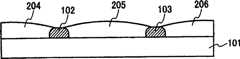
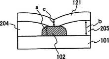
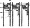
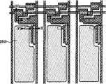
根据本发明的一个方面,在基板之上形成多个导电层,且形成绝缘层以填充导电层的间隙。According to an aspect of the present invention, a plurality of conductive layers are formed over a substrate, and an insulating layer is formed to fill gaps of the conductive layers.
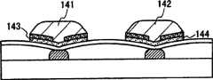
根据本发明的另一方面,在基板之上形成多个导电层,形成第一绝缘层以填充导电层的间隙,并在多个导电层和填充导电层间隙的第一绝缘层之上形成第二绝缘层。According to another aspect of the present invention, a plurality of conductive layers are formed on the substrate, a first insulating layer is formed to fill the gaps of the conductive layers, and a second insulating layer is formed on the plurality of conductive layers and the first insulating layer filling the gaps of the conductive layers. Two insulating layers.
根据本发明的再一方面,在基板之上形成多个导电层,形成第一绝缘层以填充导电层的间隙,并在部分多个导电层和邻接导电层的部分第一绝缘层之上形成第二绝缘层。According to still another aspect of the present invention, a plurality of conductive layers are formed on the substrate, a first insulating layer is formed to fill gaps in the conductive layers, and a portion of the plurality of conductive layers and a portion of the first insulating layer adjacent to the conductive layers are formed. Second insulating layer.
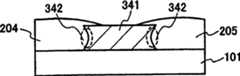
根据本发明,一种半导体装置的制造方法,包括如下步骤:在基板之上形成多个第一导电层;形成第一绝缘层以填充多个第一导电层的间隙;在第一绝缘层和多个第一导电层之上形成第二绝缘层;以及在第二绝缘层之上形成半导体区和第二导电层。According to the present invention, a method for manufacturing a semiconductor device includes the following steps: forming a plurality of first conductive layers on a substrate; forming a first insulating layer to fill gaps between the plurality of first conductive layers; A second insulating layer is formed over the plurality of first conductive layers; and a semiconductor region and the second conductive layer are formed over the second insulating layer.
根据本发明,一种半导体装置的制造方法,包括如下步骤:在基板之上形成多个第一导电层;形成第一绝缘层以覆盖多个第一导电层的一侧;在第一绝缘层和多个第一导电层之上形成第二绝缘层;以及在第二绝缘层之上形成半导体区和第二导电层。According to the present invention, a method for manufacturing a semiconductor device includes the following steps: forming a plurality of first conductive layers on a substrate; forming a first insulating layer to cover one side of the plurality of first conductive layers; forming a second insulating layer over the plurality of first conductive layers; and forming a semiconductor region and the second conductive layer over the second insulating layer.
根据本发明,一种半导体装置的制造方法,包括如下步骤:在基板之上形成多个第一导电层;通过在多个第一导电层之间喷射绝缘材料而形成第一绝缘层;在第一绝缘层和多个第一导电层之上形成第二绝缘层;以及在第二绝缘层之上形成半导体区和第二导电层。According to the present invention, a method for manufacturing a semiconductor device includes the following steps: forming a plurality of first conductive layers on a substrate; forming a first insulating layer by spraying an insulating material between the plurality of first conductive layers; forming a second insulating layer over an insulating layer and a plurality of first conductive layers; and forming a semiconductor region and a second conductive layer over the second insulating layer.
形成所谓的底栅TFT,其中第一导电层用作栅电极,第二绝缘层用作栅绝缘膜,且第二导电层用作源电极和漏电极。源区和漏区可形成在半导体区和第二导电层之间。A so-called bottom-gate TFT is formed in which the first conductive layer is used as a gate electrode, the second insulating layer is used as a gate insulating film, and the second conductive layer is used as a source electrode and a drain electrode. A source region and a drain region may be formed between the semiconductor region and the second conductive layer.
形成所谓的顶栅TFT,其中第一导电层用作源电极和漏电极,第二绝缘膜用作栅绝缘膜,且第二导电层用栅电极。源区和漏区可形成在第二导电层和半导体区之间。A so-called top-gate TFT is formed in which the first conductive layer is used as the source electrode and the drain electrode, the second insulating film is used as the gate insulating film, and the second conductive layer is used as the gate electrode. A source region and a drain region may be formed between the second conductive layer and the semiconductor region.
根据本发明,一种半导体装置的制造方法,包括如下步骤:在基板之上形成多个第一导电层;通过在多个第一导电层之间喷射绝缘材料形成第一绝缘层;在部分第一绝缘层和部分多个第一导电层之上形成第二绝缘层;并在第二绝缘层和第一导电层之上形成半导体区。According to the present invention, a method for manufacturing a semiconductor device includes the following steps: forming a plurality of first conductive layers on a substrate; forming a first insulating layer by spraying an insulating material between the plurality of first conductive layers; A second insulating layer is formed on the insulating layer and part of the plurality of first conductive layers; and a semiconductor region is formed on the second insulating layer and the first conductive layer.
形成所谓的底栅共面TFT,其中第一导电层用作栅电极、源电极和漏电极,且第二绝缘层用作栅绝缘膜。源区和漏区可形成在半导体区与源电极、漏电极之间。A so-called bottom-gate coplanar TFT is formed in which the first conductive layer serves as a gate electrode, source electrode, and drain electrode, and the second insulating layer serves as a gate insulating film. Source and drain regions may be formed between the semiconductor region and the source and drain electrodes.
根据本发明,一种半导体装置,包括:形成于绝缘表面之上的多个第一导电层;形成于多个第一导电层之间的第一绝缘层;形成于多个第一导电层和第一绝缘层表面上的第二绝缘层;形成于第二绝缘层之上的半导体区;和提供于半导体区之上的第二导电层;其中半导体区具有与第一导电层、第一绝缘层和第二绝缘层相交迭的第一区域以及与第一导电层和第二绝缘层相交迭的第二区域。According to the present invention, a semiconductor device includes: a plurality of first conductive layers formed on an insulating surface; a first insulating layer formed between the plurality of first conductive layers; a first insulating layer formed between the plurality of first conductive layers and A second insulating layer on the surface of the first insulating layer; a semiconductor region formed on the second insulating layer; and a second conductive layer provided on the semiconductor region; wherein the semiconductor region has a A first region where the layer overlaps the second insulating layer and a second region where the first conductive layer overlaps the second insulating layer.
在第一导电层的厚度大于第一绝缘层厚度的情况下,第一绝缘层的厚度b和第一导电层的厚度a之间的比b/a(b<a)为大于等于0.7且小于等于1。In the case where the thickness of the first conductive layer is greater than the thickness of the first insulating layer, the ratio b/a (b<a) between the thickness b of the first insulating layer and the thickness a of the first conductive layer is greater than or equal to 0.7 and less than is equal to 1.
在第一导电层的厚度小于第一绝缘层厚度的情况下,第一绝缘层和第一导电层之间的厚度差b-a比第二绝缘层的厚度c小,即,满足关系0<b-a<c(b<a)。In the case where the thickness of the first conductive layer is smaller than the thickness of the first insulating layer, the thickness difference b-a between the first insulating layer and the first conductive layer is smaller than the thickness c of the second insulating layer, that is, the relationship 0<b-a< c(b<a).
第一绝缘层沿着第一导电层的一侧膨胀。即,第一绝缘层形成为相对于绝缘表面的凹形。The first insulating layer expands along one side of the first conductive layer. That is, the first insulating layer is formed in a concave shape with respect to the insulating surface.
另一方面,与第一导电层接触的第一绝缘层的区域具有沿着第一导电层侧的凹痕。即,第一绝缘层形成为相对绝缘表面的凸形。On the other hand, the region of the first insulating layer in contact with the first conductive layer has a dimple along the side of the first conductive layer. That is, the first insulating layer is formed in a convex shape relative to the insulating surface.
而且,第一导电层相对绝缘表面的接触角为大于等于70°且小于等于135°。Also, the contact angle of the first conductive layer with respect to the insulating surface is greater than or equal to 70° and less than or equal to 135°.
在本发明中,作为半导体装置,可以指定集成电路、显示装置、无线标签、IC标签等,其每一个都由半导体元件组成。作为显示装置,可以典型地指定液晶显示装置、发光显示装置、DMD(数字微镜装置)、PDP(等离子体显示面板)、FED(场发射显示器)和电泳显示装置(电子纸)等。TFT是正交错(forward staggered)TFT、反交错TFT(沟道蚀刻TFT或沟道保护TFT)、底栅TFT的共面TFT等。In the present invention, as the semiconductor device, an integrated circuit, a display device, a wireless tag, an IC tag, and the like can be specified, each of which is composed of a semiconductor element. As the display device, a liquid crystal display device, a light-emitting display device, a DMD (Digital Micromirror Device), a PDP (Plasma Display Panel), an FED (Field Emission Display), an electrophoretic display device (electronic paper), and the like can typically be specified. The TFT is forward staggered TFT, reverse staggered TFT (channel etching TFT or channel protection TFT), coplanar TFT of bottom gate TFT, etc.
如其中使用的,术语“显示装置”指的是使用显示元件的装置,即图像显示装置。而且,贴附有连接体如FPC(柔性印刷电路)、TAB(载带自动焊接)或TCP(载带封装)的模块、具有在其端部上装配印刷线路板的TAB或TCP的模块、和直接通过COG(玻璃上芯片)用IC(集成电路)安装的模块都包括在显示装置中。As used therein, the term "display device" refers to a device using a display element, ie, an image display device. Also, a module to which a connecting body such as FPC (Flexible Printed Circuit), TAB (Tape Automated Bonding) or TCP (Tape Carrier Package) is attached, a module having TAB or TCP fitted with a printed wiring board on its end, and Modules mounted with ICs (Integrated Circuits) directly through COG (Chip On Glass) are included in the display device.
根据本发明,提供了液晶电视或EL电视,其每一个都由前述的半导体装置组成。According to the present invention, there is provided a liquid crystal television or an EL television, each of which is composed of the aforementioned semiconductor device.
根据本发明,通过绝缘层填充多个导电层的间隙可以减少形成于绝缘层之上的栅绝缘膜的不规则性,且由此可以提高阶梯覆盖。因此,可以防止导电边缘之上的分级切削(step cut),且可以提高具有导电层和栅绝缘膜的半导体装置的制造产量。According to the present invention, filling the gaps of the plurality of conductive layers with the insulating layer can reduce the irregularity of the gate insulating film formed over the insulating layer, and thus the step coverage can be improved. Therefore, step cut above the conductive edge can be prevented, and the manufacturing yield of the semiconductor device having the conductive layer and the gate insulating film can be improved.
由于根据本发明的半导体装置可以增加栅绝缘层厚度的均匀性,所以可以提高栅绝缘膜的耐压性,且还可以提高半导体装置的可靠性。Since the semiconductor device according to the present invention can increase the uniformity of the thickness of the gate insulating layer, the withstand voltage of the gate insulating film can be improved, and the reliability of the semiconductor device can also be improved.
在不形成具有锥形部分的栅电极的情况下,可以形成具有高的阶梯覆盖和高抗压性的栅绝缘膜,其方式可以应用到各种工艺上。Without forming a gate electrode having a tapered portion, a gate insulating film having high step coverage and high pressure resistance can be formed in a manner that can be applied to various processes.
通过由液滴喷射形成填充多个导电层间隙的栅绝缘膜,通过改变基板和喷嘴的相对位置可以将液滴滴入预定位置,该喷嘴是包含这些膜材料的液滴的喷射口。喷嘴直径、液滴的喷射速率以及喷嘴和液滴喷射的基板的移动速度之间的相对关系可以调节要形成的图案的厚度或宽度。因此,即使当使用边长为1至2m或以上的大基板时,也可以通过高精确度的喷射在所希望位置形成绝缘膜。而且,由于不使用光刻工艺可以在预定位置形成绝缘层,所以可以减小制造工艺的数目,可以提高生产量,且可以降低成本。By forming a gate insulating film filling the gaps of a plurality of conductive layers by liquid droplet ejection, liquid droplets can be dropped into predetermined positions by changing the relative positions of the substrate and nozzles, which are ejection ports for liquid droplets containing these film materials. The relative relationship between the diameter of the nozzle, the ejection rate of the droplets, and the moving speed of the nozzle and the substrate from which the droplets are ejected can adjust the thickness or width of the pattern to be formed. Therefore, even when a large substrate having a side length of 1 to 2 m or more is used, an insulating film can be formed at a desired position by highly accurate spraying. Also, since the insulating layer can be formed at a predetermined position without using a photolithography process, the number of manufacturing processes can be reduced, throughput can be improved, and cost can be reduced.
而且,可以以低成本、高生产量和高制造产量制造具有由前述工艺制造的半导体装置的液晶电视和EL电视。Furthermore, liquid crystal televisions and EL televisions having semiconductor devices manufactured by the aforementioned process can be manufactured at low cost, high throughput, and high manufacturing yield.
结合附图阅读以下详细的说明后,本发明的这些和其它目的、特征和优点将变得显而易见。These and other objects, features and advantages of the present invention will become apparent upon reading the following detailed description in conjunction with the accompanying drawings.
附图说明Description of drawings
图1A至1E是用于示出根据本发明的半导体装置的制造工艺的说明性剖面图;1A to 1E are explanatory cross-sectional views for showing a manufacturing process of a semiconductor device according to the present invention;
图2A至2E是用于示出根据本发明的半导体装置的制造工艺的说明性剖面图;2A to 2E are explanatory cross-sectional views for showing a manufacturing process of a semiconductor device according to the present invention;
图3A至3E是用于示出根据本发明的半导体装置的第一导电层结构的说明性剖面图;3A to 3E are explanatory cross-sectional views for showing the structure of the first conductive layer of the semiconductor device according to the present invention;
图4A和4B是用于示出根据本发明的半导体装置的第一绝缘层结构的说明性剖面图;4A and 4B are explanatory cross-sectional views for showing a structure of a first insulating layer of a semiconductor device according to the present invention;
图5A至5D是用于示出根据本发明的半导体装置的制造工艺的说明性剖面图;5A to 5D are explanatory cross-sectional views for showing the manufacturing process of the semiconductor device according to the present invention;
图6A至6D是用于示出根据本发明的半导体装置的制造工艺的说明性剖面图;6A to 6D are explanatory cross-sectional views for showing the manufacturing process of the semiconductor device according to the present invention;
图7A和7B是用于示出根据本发明的半导体装置结构的说明性剖面图;7A and 7B are explanatory cross-sectional views for showing the structure of a semiconductor device according to the present invention;
图8是用于示出可以应用到本发明的液滴喷射装置结构的说明性视图;FIG. 8 is an explanatory view for showing the structure of a droplet ejection device that can be applied to the present invention;
图9A至9C是用于示出根据本发明的显示装置驱动电路的装配方法的说明性顶视图;9A to 9C are explanatory top views for illustrating an assembly method of a display device driving circuit according to the present invention;
图10A至10D是用于示出根据本发明的显示装置驱动电路的装配方法的说明性剖面图;10A to 10D are explanatory cross-sectional views for illustrating an assembly method of a display device driving circuit according to the present invention;
图11是用于示出电子装置结构的说明性方块图;11 is an explanatory block diagram for showing the structure of an electronic device;
图12是电子装置的实例的说明性图;12 is an explanatory diagram of an example of an electronic device;
图13A和13B是电子装置的实例的说明性图;13A and 13B are explanatory diagrams of examples of electronic devices;
图14是用于示出在通过根据本发明的液晶显示面板中的TFT形成扫描线驱动电路的情况下的电路结构的图;14 is a diagram for illustrating a circuit configuration in a case where a scanning line driving circuit is formed by TFTs in a liquid crystal display panel according to the present invention;
图15是用于示出在根据本发明的液晶显示面板中的TFT形成扫描线驱动电路的情况下的电路结构的图(移位电阻电路);15 is a diagram for showing a circuit configuration in a case where TFTs in a liquid crystal display panel according to the present invention form a scanning line driving circuit (displacement resistance circuit);
图16是用于示出在根据本发明的液晶显示面板中的TFT形成扫描线驱动电路的情况下的电路结构的图(缓冲电路);16 is a diagram (buffer circuit) for showing a circuit configuration in a case where TFTs in a liquid crystal display panel according to the present invention form a scanning line driving circuit;
图17A至17E是用于示出根据本发明的半导体装置的制造工艺的说明性剖面图;17A to 17E are explanatory cross-sectional views for showing the manufacturing process of the semiconductor device according to the present invention;
图18A至18D是用于示出根据本发明的半导体装置的制造工艺的说明性剖面图;18A to 18D are explanatory cross-sectional views for showing the manufacturing process of the semiconductor device according to the present invention;
图19A至19C是用于示出根据本发明的半导体装置的制造工艺的说明性剖面图;19A to 19C are explanatory cross-sectional views for showing the manufacturing process of the semiconductor device according to the present invention;
图20是用于示出根据本发明的半导体装置的制造工艺的说明性顶视图;20 is an explanatory top view for showing a manufacturing process of a semiconductor device according to the present invention;
图21是用于示出根据本发明的半导体装置的制造工艺的说明性顶视图;21 is an explanatory top view for showing a manufacturing process of a semiconductor device according to the present invention;
图22是用于示出根据本发明的半导体装置的制造工艺的说明性顶视图;22 is an explanatory top view for showing a manufacturing process of a semiconductor device according to the present invention;
图23是用于示出根据本发明的半导体装置的制造工艺的说明性顶视图;23 is an explanatory top view for showing a manufacturing process of a semiconductor device according to the present invention;
图24A和24C是用于示出根据本发明的发光显示面板结构的说明性顶视图和剖面图;24A and 24C are explanatory top views and sectional views for showing the structure of a light emitting display panel according to the present invention;
图25A和25B是用于示出可以应用到本发明的液滴喷射的说明性视图;25A and 25B are explanatory views for showing droplet ejection that can be applied to the present invention;
图26是用于示出根据本发明的液晶显示模块结构的说明性视图;26 is an explanatory view for showing the structure of a liquid crystal display module according to the present invention;
图27A至27C是用于示出根据本发明的半导体装置的制造工艺的说明性剖面图;27A to 27C are explanatory cross-sectional views for showing the manufacturing process of the semiconductor device according to the present invention;
图28A至28C是用于示出根据本发明的半导体装置的制造工艺的说明性剖面图;28A to 28C are explanatory cross-sectional views for showing the manufacturing process of the semiconductor device according to the present invention;
图29A和29B是用于示出根据本发明的半导体装置的制造工艺的说明性剖面图;29A and 29B are explanatory cross-sectional views for showing the manufacturing process of the semiconductor device according to the present invention;
图30A和30B是用于示出根据本发明的半导体装置的制造工艺的说明性剖面图;30A and 30B are explanatory cross-sectional views for showing the manufacturing process of the semiconductor device according to the present invention;
图31是用于示出根据本发明的半导体装置的制造工艺的说明性顶视图;31 is an explanatory top view for showing a manufacturing process of a semiconductor device according to the present invention;
图32是用于示出根据本发明的半导体装置的制造工艺的说明性顶视图;32 is an explanatory top view for showing a manufacturing process of a semiconductor device according to the present invention;
图33是用于示出根据本发明的半导体装置的制造工艺的说明性顶视图;33 is an explanatory top view for showing a manufacturing process of a semiconductor device according to the present invention;
图34是用于示出根据本发明的半导体装置的制造工艺的说明性顶视图;34 is an explanatory top view for showing a manufacturing process of a semiconductor device according to the present invention;
图35A至35C是用于示出根据本发明的发光显示模块结构的说明性视图;35A to 35C are explanatory views for showing the structure of a light emitting display module according to the present invention;
图36A至36D是用于示出可以应用到本发明的发光元件的模式的说明性视图;36A to 36D are explanatory views for showing modes of light-emitting elements that can be applied to the present invention;
图37A至37F是用于示出可以应用到根据本发明的发光显示面板上的像素结构的说明性剖面图;37A to 37F are explanatory cross-sectional views for showing a pixel structure that can be applied to a light-emitting display panel according to the present invention;
图38A至38E是用于示出根据本发明的半导体装置结构的说明性表面图;38A to 38E are explanatory surface views for showing the structure of a semiconductor device according to the present invention;
图39A和39B是用于示出根据本发明的半导体装置结构的说明性剖面图。39A and 39B are explanatory cross-sectional views for showing the structure of a semiconductor device according to the present invention.
具体实施方式Detailed ways
实施例1Example 1
在该实施例中,参考图1A至1E、4A、4B、7A和39A说明了半导体装置和半导体装置的制造工艺,该半导体装置包括填充在多个导电层之间的绝缘层且其具有比导电层低的高度。在该实施例中,在底栅TFT中使用沟道蚀刻TFT作为半导体装置。In this embodiment, a semiconductor device including an insulating layer filled between a plurality of conductive layers and having a specific conductivity and a manufacturing process of the semiconductor device are described with reference to FIGS. The height of the low layer. In this embodiment, a channel-etched TFT is used as a semiconductor device among bottom-gate TFTs.
如图1A所示,在基板101上形成多个第一导电层102、103,且形成第一绝缘层104至106来填充在多个第一导电层102、103之间。As shown in FIG. 1A , a plurality of first
作为基板101,可以使用由绝缘物质如玻璃、石英或氧化铝制成的基板、能够抵抗后续工艺中处理温度的具有耐热性的塑料基板、硅晶片、金属板等。在该情况下,优选提供用于防止自基板分散的杂质的绝缘膜,如氧化硅(SiOx)、氮化硅(SiNx)、氮氧化硅(SiOxNy)(x>y)或氧氮化硅(SiNxOy)(x>y)。可选地,可以使用通过在金属基板如不锈钢或半导体基板的表面上形成绝缘膜如氧化硅或氮化硅制备的基板。在基板101为玻璃基板的情况下,可以使用320×400mm、370×470mm、550×650mm、600×720mm、680×880mm、1000×1200mm、1100×1250mm或1150×1300mm的大基板。在该情况下,使用玻璃基板作为基板101。As the
在使用塑料基板作为基板101的情况下,使用了PC(聚碳酸酯)、PES(聚(醚砜))(poly(ether sulfone))、PET(聚(对苯二甲酸亚乙酯))或PEN聚萘二甲酸乙二醇酯(poly(ethylene naphthalate)),其每一个都具有相对高的玻璃转变点。In the case of using a plastic substrate as the
作为第一导电层102、103的材料,使用了具有导电特性的材料。第一导电层102、103通过液滴喷射、印刷、电镀、PVD(物理气相淀积)、CVD(化学气相淀积)、气相淀积等形成。在使用PVD、CVD、气相淀积等情况下,在通过前述方法淀积后将第一导电层102、103蚀刻成希望的形状。As the material of the first
作为具有导电特性的材料,适当地使用了金属如Ag、Au、Cu、Ni、Pt、Pd、Ir、Rh、W、Al、Ta、Mo、Cd、Zn、Fe、Ti、Si、Ge、Zr或Ba;氧化铟锡(ITO)、氧化锌(ZnO)、氧化锌锡(IZO)、掺杂镓的氧化锌(GZO)、含氧化硅的氧化锌铟、有机铟、有机锡,使用其每一个作为透明的导电膜;氮化钛(TiN)等。可选地,可堆叠由这些材料制成的导电层作为第一导电层102、103。As materials having conductive properties, metals such as Ag, Au, Cu, Ni, Pt, Pd, Ir, Rh, W, Al, Ta, Mo, Cd, Zn, Fe, Ti, Si, Ge, Zr are suitably used or Ba; indium tin oxide (ITO), zinc oxide (ZnO), zinc tin oxide (IZO), gallium-doped zinc oxide (GZO), silicon oxide-containing zinc indium oxide, organic indium, organic tin, using each One as a transparent conductive film; titanium nitride (TiN), etc. Alternatively, conductive layers made of these materials may be stacked as the first
在通过液滴喷射形成第一导电层的情况下,使用溶解或分散在溶剂中的导体作为自喷射口喷射的合成物。作为导体,可以使用具有导电特性的上述材料的金属、卤化银细粒或分散的纳米颗粒。In the case of forming the first conductive layer by droplet ejection, a conductor dissolved or dispersed in a solvent is used as the composition ejected from the ejection port. As the conductor, metals, silver halide fine particles, or dispersed nanoparticles of the above materials having conductive properties can be used.
作为自喷射口喷射的合成物,考虑到具体的电阻值优选使用溶解或分散在溶剂中的金、银和铜中任意一种。而且优选地,使用低电阻且廉价的银或铜。在使用铜的情况下,另外可提供阻挡膜来防止由于杂质引起的沾污。作为溶剂,可使用有机溶剂,例如酯诸如醋酸丁酯和乙酸乙酯、乙醇诸如异丙醇和乙醇、丁酮或丙酮。As the composition ejected from the ejection port, any one of gold, silver, and copper dissolved or dispersed in a solvent is preferably used in consideration of a specific resistance value. Also preferably, low-resistance and inexpensive silver or copper is used. In the case of using copper, a barrier film may additionally be provided to prevent contamination due to impurities. As the solvent, organic solvents such as esters such as butyl acetate and ethyl acetate, ethanol such as isopropanol and ethanol, methyl ethyl ketone or acetone can be used.
对于在使用铜作布线的情况下的阻挡膜,可优选使用含氮的绝缘或导电材料,如氮化硅、氮氧化硅、氮化铝、氮化钛或氮化钽通过液滴喷射形成。For the barrier film in the case of using copper as the wiring, an insulating or conductive material containing nitrogen, such as silicon nitride, silicon oxynitride, aluminum nitride, titanium nitride, or tantalum nitride, can be preferably formed by droplet discharge.
对于液滴喷射使用的合成物优选具有5至20mPa·s的粘度,这是由于这样能够防止合成物干燥且合成物能够从喷射口平滑地喷射。而且,合成物优选具有40mN/m或更小的表面张力。合成物的粘度等可根据溶剂或用途适当地调节。例如,通过在溶剂中溶解或分散ITO、ZnO、IZO、GZO、含氧化硅的氧化铟锡、有机铟或有机锡制备的合成物具有5至50mPa·s的粘度,通过在溶剂中溶解或分散银制备的合成物具有5至20mPa·s的粘度,且通过在溶剂中溶解或分散金制备的合成物具有10至20mPa·s的粘度。The composition used for droplet ejection preferably has a viscosity of 5 to 20 mPa·s, since drying of the composition can be prevented and the composition can be ejected smoothly from the ejection port. Also, the composition preferably has a surface tension of 40 mN/m or less. The viscosity and the like of the composition can be appropriately adjusted according to the solvent or use. For example, a composition prepared by dissolving or dispersing ITO, ZnO, IZO, GZO, silicon oxide-containing indium tin oxide, organic indium, or organic tin in a solvent has a viscosity of 5 to 50 mPa·s, and by dissolving or dispersing in a solvent The composition prepared by silver has a viscosity of 5 to 20 mPa·s, and the composition prepared by dissolving or dispersing gold in a solvent has a viscosity of 10 to 20 mPa·s.
为了防止喷嘴堵塞和制造高清晰度的图案,虽然依赖于每个喷嘴的直径、希望的图案形状等,但导体颗粒的直径优选尽可能小,例如0.1μm或更小。通过公知的方法如电解法、雾化法或湿法减小法形成合成物,以通常具有约0.5至10μm的颗粒大小。注意,在通过气体蒸发法形成合成物的情况下,通过分散剂保护的纳米颗粒具有约7nm的细粒直径。另外,在每个纳米颗粒都通过覆盖材料保护的情况下,室温时纳米颗粒未聚集地稳定分散在溶液中且性能类似于液体。因此,优选使用覆盖材料。In order to prevent nozzle clogging and produce high-definition patterns, although depending on the diameter of each nozzle, desired pattern shape, etc., the diameter of the conductor particles is preferably as small as possible, for example, 0.1 μm or less. The composition is formed by known methods such as electrolysis, atomization or wet reduction to generally have a particle size of about 0.5 to 10 μm. Note that in the case of forming the composition by the gas evaporation method, the nanoparticles protected by the dispersant have a fine particle diameter of about 7 nm. In addition, in the case where each nanoparticle is protected by the covering material, the nanoparticles are stably dispersed in the solution without aggregation and behave like a liquid at room temperature. Therefore, a covering material is preferably used.
由于在合成物喷射到物体上期间合成物的溶剂蒸发,所以可在减压下进行合成物的喷射工艺。因此,可以省略或缩短干燥和烘焙的后续工艺。在喷射溶液后,在常压或减压下根据溶液的材料通过激光照射、快速热退火、加热炉等进行干燥和/或烘焙的处理。干燥和烘焙的每个工艺是热处理的工艺。例如,在100℃进行干燥处理达三分钟,而在200至350℃的温度下进行烘焙达15至120分钟,其每一个都具有不同的目的、温度和周期。为了顺利地进行干燥和烘焙处理,虽然依赖于基板的材料,但基板可加热到100至800℃(优选,200至350℃)。根据工艺,通过蒸发溶液中的溶剂或化学地移除分散剂产生硬化和收缩的外围树脂来加速熔融和焊接。在氧或氮或大气的情况下进行处理。优选在有氧的情况下进行处理(在该情况下易于移除溶解或分散有金属元素的溶剂)。由有机物质制成的粘合剂根据加热温度、大气和时间留在导电层中。Since the solvent of the composition evaporates during the spraying of the composition onto the object, the spraying process of the composition may be performed under reduced pressure. Therefore, subsequent processes of drying and baking can be omitted or shortened. After spraying the solution, drying and/or baking are performed by laser irradiation, rapid thermal annealing, heating furnace, etc. under normal pressure or reduced pressure depending on the material of the solution. Each process of drying and baking is a process of heat treatment. For example, drying treatment is performed at 100° C. for three minutes, and baking is performed at a temperature of 200 to 350° C. for 15 to 120 minutes, each of which has a different purpose, temperature, and period. In order to smoothly perform the drying and baking process, although depending on the material of the substrate, the substrate may be heated to 100 to 800°C (preferably, 200 to 350°C). Depending on the process, melting and welding are accelerated by evaporating the solvent from the solution or chemically removing the dispersant to produce a hardened and shrunken peripheral resin. Treat under oxygen or nitrogen or atmosphere. The treatment is preferably carried out in the presence of oxygen (in which case the solvent in which the metal element is dissolved or dispersed is easily removed). The adhesive made of organic substances remains in the conductive layer depending on heating temperature, atmosphere and time.
在该实施例中,通过选择性地喷射分散有几nm银颗粒的溶液(以下,Ag浆料)形成含有银作为其主要成分的导电层,以烘干和烘焙作为第一导电层102、103。通过三维不规则地重叠导电细粒形成第一导电层。即,通过三维的聚集颗粒形成第一导电层。因此,其表面具有微观的不规则性。由于Ag浆料的温度和加热时间,细粒熔融为由细粒形成的聚集体。随着Ag浆料的温度和加热时间增加了聚集体的尺寸,且因此表面的高度差很大。细粒熔融的区域成为多晶结构。In this embodiment, a conductive layer containing silver as its main component is formed by selectively spraying a solution in which silver particles of several nm are dispersed (hereinafter, Ag paste) to dry and bake as the first
作为第一绝缘层104至106,通过液滴喷射、喷墨、旋涂、辊涂、槽涂(slot coating)等形成绝缘材料来填充多个第一导电层102、103的间隙。在使用液滴喷射、喷墨等的情况下,将用于第一绝缘层的材料喷射到预定的位置。在利用旋涂、辊涂、槽涂等的情况下,通过适当地调节第一材料的粘度、表面张力等形成第一绝缘层以暴露部分的(上部的)第一导电层。As the first insulating
作为第一绝缘层104至106的材料的典型实例,可以指定聚酰亚胺、丙烯酸、酚醛清漆树脂、蜜胺树脂、酚醛树脂、环氧树脂、硅树脂、呋喃树脂和邻苯二甲酸二烯丙基树脂。可选地,可以使用分散有无机氧化物细粒的溶液、PSG(磷玻璃)、BPSG(硼磷硅玻璃)、薄膜、硅酸盐SOG(玻璃上旋涂)、烷氧基硅酸盐SOG、聚硅氨烷SOG、如由聚甲基硅氧烷代表的具有Si-CH3键的SiO2。As typical examples of the materials of the first insulating
在此,参考图4A、4B和7A说明第一绝缘层104至106的形状。如图7A所示,第一绝缘层104和105具有比第一导电层102的厚度a薄的厚度b。通常,b/a(b<a)的比,即第一绝缘层104、105的厚度b与第一导电层102的厚度a的比优选为大于等于0.7至小于等于1。在第一绝缘层104、105的厚度b与第一导电层102的厚度a的比在前述范围内的情况下,第二绝缘层可以形成有很少的不规则性,提高了薄膜厚度的均匀性,且提高了阶梯覆盖。因此,可以以高产量制造具有高耐压和几乎无漏电流的半导体装置。Here, the shapes of the first insulating
参考图4A和4B说明与第一导电层102接触的绝缘层104、105的形状。图1A至1E中的第一绝缘层104、105分别由图4A中的附图标记401、402表示,且图4B中的分别由411、412表示。The shapes of the insulating
如图4A所示,第一绝缘层401、402沿着第一导电层102的一侧膨胀。即,与第一导电层102接触的第一绝缘层的第一区域403比不与第一导电层102接触的第一绝缘层的第二区域404膨胀得高。换句话说,第一绝缘层401、402相对于基板101的表面形成了凹形。可以利用具有较低粘度的绝缘材料形成具有这种形状的绝缘层401、402。As shown in FIG. 4A , the first insulating
另一方面,如图4B所示,第一绝缘层411、412的区域在与第一导电层102接触的区域处凹陷。即,使与第一导电层102接触的第一绝缘层的第一区域413凹陷得比没与第一导电层102接触的第一绝缘层的第二区域413低。换句话说,第一绝缘层411、412形成相对于基板101的凸形。可以利用具有较高粘度的绝缘材料形成具有这种形状的绝缘层411、412。On the other hand, as shown in FIG. 4B , regions of the first insulating
如图1B所示,在第一导电层102、103和第一绝缘层104至106之上形成用作栅绝缘膜的第二绝缘层121、具有导电特性的第一半导体膜122和第二半导体膜123。As shown in FIG. 1B, a second insulating
通过薄膜形成法如等离子体CVD或溅射形成第二绝缘层121,以具有包含氮化硅、氧化硅或另外的硅的单层或叠层的结构。而且,优选第二绝缘层形成为通过自与栅电极接触的一侧层叠氮化硅膜(氧氮化硅膜)、氧化硅膜和氮化硅膜(氧氮化硅膜)的叠层结构。栅电极与该结构中的氮化硅膜接触,由此可以防止由于氧化引起的劣化。The second
而且,可以通过液滴喷射、涂覆、溶胶-凝胶等利用具有绝缘特性的溶液形成第二绝缘层121。作为具有绝缘特性的溶液的典型实例,可以适当地使用分散有无机氧化物细粒的溶液、聚酰亚胺、聚酰胺、聚酯、丙烯酸、PSG(磷玻璃)、BPSG(硼磷硅玻璃)、薄膜、硅酸盐SOG(玻璃上旋涂)、烷氧基硅酸盐SOG、聚硅氨烷SOG、如由聚甲基硅氧烷代表的具有Si-CH3键的SiO2。Also, the second insulating
可以由具有选自由非晶半导体、通过混合非晶态和晶态形成的半非晶半导体(可称作为SAS)、其中可以在非晶半导体中观察到0.5至20nm晶粒的微晶半导体和结晶半导体构成的组中的态的膜形成第一半导体膜122。将其中可以观察到0.5至20nm晶粒的微晶半导体称作为微晶(μc)。作为包含硅、硅锗(SiGe)等作为其主成分的膜,可以使用10至60nm厚度的半导体膜。It can be made of a semi-amorphous semiconductor (may be referred to as SAS) which is selected from an amorphous semiconductor, a semi-amorphous semiconductor (may be referred to as SAS) in which crystal grains of 0.5 to 20 nm can be observed in an amorphous semiconductor, and a crystalline Films in the state of the semiconductor group form the
SAS具有介于非晶结构和结晶结构(包含单晶和多晶)之间的中间结构。SAS具有相对于自由能的稳定的第三态和具有短程有序和晶格畸变的结晶区。至少一部分膜包括0.5至20nm的结晶区。在SAS包括硅作为其主要成分的情况下,拉曼光谱移动到比520cm-1低的波数。通过X-射线衍射,观察到了可自硅晶格得到的衍射峰(111)、(220)。在SAS中包含了1原子%或更多的氢或卤素作为悬挂键的中和剂。SAS has an intermediate structure between an amorphous structure and a crystalline structure (including single crystal and polycrystal). SAS has a stable third state with respect to free energy and crystalline regions with short-range order and lattice distortion. At least a portion of the film includes crystalline regions of 0.5 to 20 nm. In the case of SAS including silicon as its main component, the Raman spectrum is shifted to lower wavenumbers than 520 cm−1 . By X-ray diffraction, the diffraction peaks (111), (220) obtainable from the silicon lattice were observed. 1 atomic % or more of hydrogen or halogen is contained in SAS as a neutralizing agent for dangling bonds.
通过辉光放电分解硅化物气体可以获得SAS。作为硅化物气体的典型实例,指定了SiH4。可选地,可以使用Si2H6、SiH2Cl2、SiHCl3、SiCl4、SiF4等。通过被氢或氟、或氢或氟和选自由氦、氩、氪和氖构成的组中的一种或多种稀有气体元素稀释硅化物气体容易形成SAS。优选用在10至1000倍范围内的稀释率稀释硅化物气体。可选地,可以利用由氦气体稀释的Si2H6和GeF4来形成SAS。通过辉光放电分解反应的膜的生产优选在减压下进行。施加的电压在0.1至133Pa的范围内。可提供1至120MHz范围内的高频功率,优选13至60MHz来用于产生辉光放电分解的功率。基板的加热温度为300℃或更小,优选100至250℃。SAS can be obtained by decomposing silicide gas by glow discharge. As a typical example of the silicide gas, SiH4 is specified. Alternatively, Si2 H6 , SiH2 Cl2 , SiHCl3 , SiCl4 , SiF4 , etc. may be used. SAS is easily formed by diluting the silicide gas with hydrogen or fluorine, or hydrogen or fluorine and one or more rare gas elements selected from the group consisting of helium, argon, krypton, and neon. The silicide gas is preferably diluted with a dilution rate in the range of 10 to 1000 times. Alternatively, SAS can be formed using Si2 H6 and GeF4 diluted with helium gas. The production of membranes by glow discharge decomposition reactions is preferably carried out under reduced pressure. The applied voltage is in the range of 0.1 to 133Pa. High frequency power in the range of 1 to 120 MHz, preferably 13 to 60 MHz, can be supplied for generating the power for glow discharge decomposition. The heating temperature of the substrate is 300°C or less, preferably 100 to 250°C.
可以通过非晶半导体膜的结晶或通过加热或激光照射SAS来形成结晶半导体膜。可选地,可以直接形成结晶半导体膜。在该情况下,可以通过利用加热或具有氟化物气体如GeF4或F2的等离子体、或硅烷气体如SiH4或Si2H6直接形成结晶半导体膜。A crystalline semiconductor film can be formed by crystallization of an amorphous semiconductor film or by heating or irradiating SAS with laser light. Alternatively, a crystalline semiconductor film may be directly formed. In this case, the crystalline semiconductor film can be directly formed by using heating or plasma with a fluoride gas such as GeF4 or F2 , or a silane gas such as SiH4 or Si2 H6 .
第二半导体膜123具有导电特性。在形成n沟道型TFT的情况下,掺杂了周期表中的15族元素,典型地为磷或砷。在形成p沟道型TFT的情况下,掺杂了周期表中的13族元素,典型地为硼。利用包含周期表中的13或15族元素如硼、磷或砷的气体的硅化物气体通过等离子体CVD来形成第二半导体膜123。而且,在形成半导体膜后,可以通过在要用激光照射的半导体膜之上涂布包含周期表中的13或15族元素的溶液来形成具有导电特性的第二半导体膜。作为激光束,适当地使用了自公知的脉冲或连续振荡激光器发出的激光束。The
如图1C所示,在半导体膜123之上形成第一掩模图案131至134。第一掩模图案优选通过耐热的高分子材料的液滴喷射形成,该材料包括作为主链的芳香环或环状环,且包括具有少许脂肪族基的高极性不同的原子量。作为这种高分子材料的典型实例,可以指定聚酰亚胺或聚苯并咪唑。在利用聚酰亚胺的情况下,可以通过在第二半导体膜123之上自喷射口喷射包含聚酰亚胺的溶液并在200℃烘焙30分钟,来形成第一掩模图案131至134。As shown in FIG. 1C ,
而且,可以通过预先提供具有液体脱落表面的掩模图案和将高分子材料涂布或喷射到未被液体脱落表面覆盖的区域上来形成第一掩模图案。Also, the first mask pattern may be formed by previously providing a mask pattern having a liquid release surface and coating or spraying a polymer material onto a region not covered by the liquid release surface.
然后,通过利用第一掩模图案131至134蚀刻第二半导体膜123来形成第一半导体区(也称作为源区或漏区或接触层)135至138。其后,移除第一掩模图案。Then, first semiconductor regions (also referred to as source or drain regions or contact layers) 135 to 138 are formed by etching the
可以通过利用氯化物气体如典型的为Cl2、BCl3、SiCl4或CCL4、氟化物气体如CF4、SF6、NF3或CHF3、或O2来蚀刻第二半导体膜。The second semiconductor film can be etched by using a chloride gas such as typically Cl2 , BCl3 , SiCl4 or CCL4 , a fluoride gas such as CF4 , SF6 , NF3 or CHF3 , or O2 .
然后,如图1D所示,在基板之上形成第二掩模图案141、142。可以通过利用与第一掩模图案相同的材料来形成第二掩模图案。Then, as shown in FIG. 1D ,
然后,通过利用第二掩模图案141、142作掩模蚀刻第一半导体膜122来形成第二半导体区(沟道形成区)143、144。作为第一半导体膜的蚀刻条件,可以用作第二半导体膜的蚀刻条件。其后,通过利用剥离器处理、利用氧灰化等来移除第二掩模图案。Then, second semiconductor regions (channel formation regions) 143, 144 are formed by etching the
图39A是第二半导体区143和第一导电层102附近的放大图。FIG. 39A is an enlarged view of the vicinity of the
图39A说明了提供有第一导电层102、填充第一导电层102外部的第一绝缘层104、105、第二绝缘层121和第二半导体区143的区域。第二半导体区143包括与第一导电层102和第二绝缘层121交迭的区域161以及与第一导电层102、第一绝缘层104和105和第二绝缘层121交迭的区域162。FIG. 39A illustrates a region provided with the first
即,根据本发明的TFT的栅绝缘膜包括由单层绝缘膜形成的区域和由两层绝缘膜形成的区域。That is, the gate insulating film of the TFT according to the present invention includes a region formed of a single insulating film and a region formed of two insulating films.
如图1D所示,可以通过印刷、喷射、液滴喷射等利用有机半导体材料形成第二半导体区143、144。在该情况下,工艺的数目可以由于不需要上述的蚀刻工艺而减小。作为本发明中使用的有机半导体材料,优选使用包含共轭双键的π-共轭的系统高分子材料。通常,可以使用可溶解的高分子材料,如聚噻吩、聚(3-烷基噻吩)、聚噻吩衍生物或并五苯。As shown in FIG. 1D , the
作为本发明中可以使用的另一有机半导体材料,可以使用形成可溶解的前驱物后被处理的可以形成第一半导体区的材料。作为通过前驱物的有机材料,可以使用聚噻吩撑亚乙烯(polythienylenevinylene)、聚(2,5-噻吩基亚乙烯)(poly(2,5-thienylenevinylene))、聚乙炔、聚乙炔衍生物、聚芳撑亚乙烯(polyarylenevinylene)等。As another organic semiconductor material that can be used in the present invention, a material capable of forming the first semiconductor region that is processed after forming a soluble precursor can be used. As the organic material passing through the precursor, polythienylene vinylene (polythienylenevinylene), poly(2,5-thienylenevinylene) (poly(2,5-thienylenevinylene)), polyacetylene, polyacetylene derivatives, poly Arylene vinylene (polyarylenevinylene) and so on.
当前驱物转化为有机半导体时,不仅进行了热处理,而且掺杂了催化剂如氯化氢气体。作为溶解这些可溶解的有机半导体材料的常用溶剂,可以使用甲苯、二甲苯、氯苯、二氯苯、茴香醚、氯仿、二氯甲烷、γ-丁基内酯、丁基溶纤剂(butyl cellosolve)、环己烷、N-甲基-2-吡咯烷酮(NMP)、环己酮、2-丁酮、二氧六环、二甲基甲酰胺(DMF)、四氢呋喃(THF)等。When the precursor is converted into an organic semiconductor, it is not only heat-treated but also doped with a catalyst such as hydrogen chloride gas. As common solvents for dissolving these soluble organic semiconductor materials, toluene, xylene, chlorobenzene, dichlorobenzene, anisole, chloroform, methylene chloride, γ-butyl lactone, butyl cellosolve can be used , cyclohexane, N-methyl-2-pyrrolidone (NMP), cyclohexanone, 2-butanone, dioxane, dimethylformamide (DMF), tetrahydrofuran (THF), etc.
在有机半导体用于第二半导体区143、144的情况下,可以形成由有机导电材料如聚乙炔、聚苯胺、PEDOT(聚乙烯二氧噻吩)或PSS(聚苯乙烯磺酸盐)制成的导电层来代替形成第一导电区135至138。导电层用作接触层或源区和漏区。In the case where an organic semiconductor is used for the
代替第一半导体区135至138,可以使用由金属元素制成的导电层。在该情况下,由于许多有机半导体材料是传输空穴作为载流子的p型半导体,所以优选使用具有高功函数的金属来制作半导体层的欧姆接触。Instead of the
具体地,希望使用金、铂、铬、钯、铝、铟、钼、镍等的金属、合金等。可以通过印刷、辊涂或液滴喷射利用这些金属或合金材料由导电浆料形成导电层。Specifically, it is desirable to use metals, alloys, and the like of gold, platinum, chromium, palladium, aluminum, indium, molybdenum, nickel, and the like. The conductive layer can be formed from a conductive paste using these metal or alloy materials by printing, roll coating, or droplet jetting.
而且,可堆叠由有机半导体材料制成的第二半导体区、由有机导电材料制成的导电层和由金属元素制成的导电层。Also, a second semiconductor region made of an organic semiconductor material, a conductive layer made of an organic conductive material, and a conductive layer made of a metal element may be stacked.
在第二半导体区由SAS制成的情况下,除了该实施例中栅电极由源区和漏区覆盖的结构外,可以形成其中源区、漏区的边缘部分和栅电极的边缘部分对准的所谓的自对准结构。而且,可以形成其中栅电极没有由源区和漏区覆盖、且源区和漏区彼此隔开一定距离的结构。在形成该结构的情况下,当TFT用于显示装置的开关元件时由于可以减小截止电流而可以增强对比度。而且,TFT可以形成为具有其中第二半导体区覆盖多个栅电极的多栅极结构。在该情况下,也可以减小截止电流。In the case where the second semiconductor region is made of SAS, in addition to the structure in which the gate electrode is covered by the source region and the drain region in this embodiment, it is possible to form a structure in which the edge portions of the source region, the drain region, and the edge portion of the gate electrode are aligned The so-called self-aligned structure. Also, it is possible to form a structure in which the gate electrode is not covered by the source region and the drain region, and the source region and the drain region are spaced apart from each other by a certain distance. In the case of forming this structure, when the TFT is used for a switching element of a display device, contrast can be enhanced since off-current can be reduced. Also, the TFT may be formed to have a multi-gate structure in which the second semiconductor region covers a plurality of gate electrodes. In this case, off-state current can also be reduced.
接下来,如图1E所示,利用导电材料在第一半导体区135至138之上形成源、漏电极151至154。源、漏电极151至154由与第一导电层相同的材料和相同的方法形成。在该情况下,通过选择性地喷射分散具有几nm颗粒尺寸的银颗粒的Ag浆料溶液和烘干来形成源、漏电极151至154。Next, as shown in FIG. 1E , source and drain
然后,优选在源、漏电极151至154之上形成钝化膜。钝化膜可以利用氮化硅、氧化硅、氧氮化硅、氮氧化硅、氮氧化铝、氧化铝、类金刚石碳(DLC)、氮化碳(CN)或其它绝缘材料通过薄膜形成法如等离子体CVD或溅射形成。Then, a passivation film is preferably formed over the source and drain
根据前述工艺,可以以高的制造产量制造具有高耐压和减小的漏电流的沟道蚀刻TFT。According to the foregoing process, a channel-etched TFT having a high withstand voltage and reduced leakage current can be manufactured with high manufacturing yield.
实施例2Example 2
在该实施例中,参考图2A、2B、7B和39B说明其中第一绝缘层具有比第一导电层更大厚度的实施例1中半导体装置的制造工艺。在该实施例中,说明底栅TFT中的沟道蚀刻TFT作为半导体装置。In this embodiment, a manufacturing process of the semiconductor device in
如图2A所示,与实施例1的情况相同,在基板101之上形成第一导电层102、103。然后,形成第一绝缘层204至206。第一绝缘层204至206具有比第一导电层102、103大的厚度且覆盖第一导电层102、103的部分侧部和顶部。As shown in FIG. 2A , as in the case of
可以通过与实施例1中的第一绝缘层104至106相同的材料和相同的方法形成第一绝缘层204至206。The first insulating
如图2B所示,与实施例1的情况相同,顺序地形成第二绝缘层221、具有导电特性的第一半导体膜122和第二半导体膜123。而且,可以通过与实施例1中的第二绝缘层121相同的材料和相同的方法形成第二绝缘层221。As shown in FIG. 2B , as in the case of
参考图7B说明第一绝缘层204至206和第二绝缘层221的厚度。如图7B所示,第一绝缘层的厚度b比第一导电层的厚度a大。因此,第一绝缘层覆盖第一导电层的部分侧部和顶部。第一绝缘层和第一导电层之间的厚度差b-a优选比第二绝缘层的厚度c小。因此,优选满足0<厚度差(b-a)<c<(b>a)的关系。在第一绝缘层204至206、第一导电层和第二绝缘层的厚度在上述范围内的情况下,第二绝缘层可以形成为具有少许的不规则性,提高了厚度的均匀性,且还提高了阶梯覆盖。因此,可以以良好的产量制造具有高耐压和几乎无漏电流的半导体装置。The thicknesses of the first insulating
其后,如图2C至2E所示,可以根据与实施例1中描述的相同的工艺形成用作源区和漏区的第一半导体区135至138、用作沟道形成区的第二半导体区143、144、源电极和漏电极151至154。Thereafter, as shown in FIGS. 2C to 2E ,
图39B是第二半导体区143和第一导电层102附近的放大图。FIG. 39B is an enlarged view of the vicinity of the
图39B说明了形成第一导电层102和填充第一导电层102的外部的第一绝缘层204、205、第二绝缘层221及第二半导体区143。第二半导体区143具有与第一导电层102和第二绝缘层221交迭的区域261,以及与第一导电层102、第一绝缘层204、205和第二绝缘层221交迭的区域262。FIG. 39B illustrates the formation of the first
因此,根据本发明的TFT的栅绝缘膜具有由单层绝缘膜形成的区域和由两层绝缘膜形成的区域。而且,根据该实施例的TFT的第二半导体区(沟道形成区)形成为具有相对于基板表面的凹形。Therefore, the gate insulating film of the TFT according to the present invention has a region formed of a single insulating film and a region formed of two insulating films. Also, the second semiconductor region (channel formation region) of the TFT according to this embodiment is formed to have a concave shape with respect to the surface of the substrate.
通过前述工艺,可以以高的制造产量制造具有高耐压和减小的漏电流的沟道蚀刻TFT。Through the foregoing process, a channel-etched TFT having a high withstand voltage and reduced leakage current can be manufactured with high manufacturing yield.
实施例3Example 3
参考图3A至3E说明可以应用到本发明实施例1或2中的第一导电层102、103的形状。该实施例结合实施例2给出说明。而且,还可以适当地使用实施例1。The shapes of the first
如图3A所示,导电膜具有在边缘部分相对于基板101接触角θ1为70至90°的锥形部分,即导电层301形成为具有梯形形状的剖面,并形成第一绝缘层204、205。常规地,存在如下问题,即在具有70°或以上的接触角θ1的膜图案之上形成膜的情况下,膜的阶梯覆盖特性退化,且随着接触角的增加产生了分级切削。然而,可以防止以后形成的膜的分级切削,且可以通过形成第一绝缘层204、205来改善膜厚度的均匀性。可以利用由公知的光刻工艺形成的掩模图案通过膜的干法蚀刻来形成具有这种形状的导电层301。As shown in FIG. 3A, the conductive film has a tapered portion with a contact angle θ1 of 70 to 90° at the edge portion relative to the
如图3B所示,形成了具有在下边缘部分相对于基板101的90°接触角θ2和在上边缘部分具有斜面部分或曲率半径部分312的导电层311。然后,形成第一绝缘层204、205。图3B说明了具有曲率半径部分312的导电层。常规地,存在如下问题,即膜的阶梯覆盖特性退化,且在具有90°的接触角θ的膜图案之上形成膜的情况下产生了分级切削。然而,通过形成第一绝缘层204、205,可以防止之后形成的膜的分级切削,且可以改善膜厚度的均匀性。可以通过液滴喷射、喷墨等喷射滴剂并干燥及烘焙来形成具有这种形状的导电层。As shown in FIG. 3B , a
如图3C所示,形成具有在下边缘部分处相对于基板101接触角θ3为90°和在上边缘部分处相对于基板101接触角θ4为90°的导电层321,即形成了具有矩形形状的剖面。然后,形成第一绝缘层204、205。常规地,存在如下问题,即膜的阶梯覆盖特性退化,且在矩形形状的膜图案之上形成膜的情况下产生了分级切削。然而,通过形成第一绝缘层204、205,可以防止之后形成的膜的分级切削,且可以改善膜厚度的均匀性。利用由公知的光刻工艺形成的掩模图案,通过膜的干法蚀刻可以形成具有这种形状的导电层321。可选地,可以使用印刷、电镀等。As shown in FIG. 3C, a
如图3D所示,形成具有相对于基板101接触角θ5为大于等于90°且小于等于135°的导电层331,即形成具有反锥形的部分。然后,形成第一绝缘层204、205。常规地,存在如下问题,即难以形成在邻近由上边缘部分覆盖的下边缘部分处的膜,由此膜的阶梯覆盖特性退化,且在具有90°或以上的接触角θ的膜图案之上形成膜的情况下产生了分级切削。然而,通过形成第一绝缘层204、205,可以防止之后形成的膜的分级切削,且可以改善膜厚度的均匀性。As shown in FIG. 3D , the
如图3E所示,在导电层341的侧面处形成了具有凹面部分342的导电层341。然后,形成第一绝缘层204、205。常规地,存在如下问题,即膜图案具有显著的不规则性,膜的阶梯覆盖特性退化,且在具有凹面部分的膜图案之上形成膜的情况下产生了分级切削。然而,通过形成第一绝缘层204、205,可以防止之后形成的膜的分级切削,且可以改善膜厚度的均匀性。利用由公知的光刻工艺形成的掩模图案,通过膜的干法蚀刻可以形成具有这种形状的导电层341。As shown in FIG. 3E , a
利用如上所述的各种形状的导电膜本发明可以形成TFT,且因此可以扩展该制造方法的可适用范围。The present invention can form a TFT using conductive films of various shapes as described above, and thus can expand the applicable range of the manufacturing method.
实施例4Example 4
在该实施例中,说明了根据本发明底栅TFT中的沟道保护型TFT的制造工艺。利用但不专门利用实施例1来形成第一绝缘层。还可以使用实施例2。而且,可以适当地使用实施例3中所述的第一导电层作为该实施例中的第一导电层。In this embodiment, a manufacturing process of a channel protection type TFT among bottom gate TFTs according to the present invention is explained. The first insulating layer was formed using, but not exclusively using, Example 1. Example 2 can also be used. Also, the first conductive layer described in Embodiment 3 may be suitably used as the first conductive layer in this embodiment.
如图5A所示,利用实施例1在基板101之上形成第一导电层102、103。形成第一绝缘层104至106来填充在第一导电层102、103之间。As shown in FIG. 5A , first
如图5B所示,在第一导电层102、103和第一绝缘层104至106之上形成用作栅绝缘膜的第二绝缘层121和第一半导体膜122。然后,在第一半导体膜122之上且分别与第一导电层102、103交迭的区域之上形成保护膜501、502。通过与如第一实施例所示的第一掩模图案131至134相同的材料和相同的方法形成保护膜501、502。As shown in FIG. 5B , a second insulating
然后,形成第二半导体膜(具有导电特性的半导体膜)523。而且,可以通过与实施例1中描述的第二半导体膜123相同的材料和相同的方法形成第二半导体膜523。Then, a second semiconductor film (semiconductor film having conductive properties) 523 is formed. Also, the
如图5C所示,形成第一掩模图案531、532。可以通过与实施例1中描述的第二掩模图案141、142相同的材料和相同的方法形成第一掩模图案531、532。As shown in FIG. 5C,
利用第一掩模图案蚀刻第一半导体膜和第二半导体膜,以形成第一半导体区533、534和第二半导体区543、544。其后,移除了第一掩模图案。The first semiconductor film and the second semiconductor film are etched using a first mask pattern to form
如图5D所示,在第一半导体区533、534之上形成了源电极和漏电极551至554。As shown in FIG. 5D , source and drain
利用源电极和漏电极551至554作掩模蚀刻并分割第一半导体区533、534的暴露部分,以形成源区和漏区535至538。利用该工艺,暴露出了保护膜501、502。The exposed portions of the
作为源区和漏区535至538的形成方法,不仅可以使用该实施例而且可以使用实施例1中所述的第一半导体区的制造工艺。可以将根据该实施例的源区和漏区的形成工艺应用到实施例1。As a method of forming the source and drain
利用前述工艺,可以以高的制造产量制造具有高耐压和减小的漏电流的沟道保护TFT。Using the foregoing process, a channel protection TFT having a high withstand voltage and reduced leakage current can be manufactured with a high manufacturing yield.
实施例5Example 5
参考图6A至6D说明了根据本发明的顶栅TFT中的前交错(forwardstaggered)TFT的制造工艺。利用但不专门利用实施例1形成第一绝缘层。还可以使用实施例2。而且,可以适当地使用实施例3中所述的第一导电层作为该实施例中的第一导电层。A manufacturing process of a forward staggered TFT among top gate TFTs according to the present invention is explained with reference to FIGS. 6A to 6D. The first insulating layer was formed using, but not exclusively using, Example 1. Example 2 can also be used. Also, the first conductive layer described in Embodiment 3 may be suitably used as the first conductive layer in this embodiment.
如图6A所示,在基板101之上形成用作源电极和漏电极的第一导电层601、602。通过适当地利用与实施例1中的第一导电层102、103相同的材料和相同的方法形成第一导电层601、602。然后,在第一导电层601、602之上形成具有导电特性的第一半导体膜603。通过与实施例1中的第二半导体膜相同的材料和相同的方法形成第一半导体膜603。然后,在第一半导体膜603之上形成第一掩模图案604、605。由于使用第一掩模图案作为掩模用于形成源区和漏区,所以通过与实施例1中的第一掩模图案131至134相同的材料和相同的方法形成第一掩模图案。As shown in FIG. 6A , first
如图6B所示,利用第一掩模图案蚀刻第一半导体膜,以形成第一半导体区611、612。第一半导体区611、612用作源区和漏区。而且,通过适当地利用与实施例1中的第一半导体区135至138相同的材料和相同的方法形成第一半导体区611、612。As shown in FIG. 6B , the first semiconductor film is etched using a first mask pattern to form
在层叠的第一导电层601、602和第一半导体区之间形成第一绝缘层613至615。通过与实施例1中的第一绝缘层104至106相同的材料和相同的制造工艺形成第一绝缘层613至615。First insulating
如图6C所示,在第一绝缘层613至615、第一导电层601、602和第一半导体区611、612之上形成第二半导体膜621。通过适当地利用与实施例1中的第一半导体膜122相同的材料和相同的制造方法形成第二半导体膜621。As shown in FIG. 6C , a
然后,在第二半导体膜621之上形成第二膜图案622。第二膜图案是用于形成沟道形成区的掩模,且适当地利用与实施例1中的第二掩模图案141、142相同的方法和相同的制造工艺形成。Then, a
然后,如图6D所示,利用第二膜图案622,通过蚀刻第二半导体膜621形成第二半导体区631。第二半导体区用作沟道形成区。Then, as shown in FIG. 6D , using the
形成第二绝缘层632和第二导电层633。由于第二绝缘层632用作栅绝缘膜,所以通过与实施例1中的第二绝缘层121相同的方法和相同的制造工艺形成第二绝缘层632。而且,由于第二导电层633用作栅电极,所以通过与实施例1中的第一导电层102、103相同的材料和相同的制造工艺形成第二导电层633。A second insulating
利用前述工艺,可以以高的制造产量制造具有高耐压和减小的漏电流的前交错TFT。Using the aforementioned process, front-staggered TFTs with high withstand voltage and reduced leakage current can be manufactured with high manufacturing yield.
实施例6Example 6
在该实施例中,参考图38A至38E说明了TFT的接触孔的形成方法。In this embodiment, a method of forming a contact hole of a TFT is explained with reference to FIGS. 38A to 38E.
根据实施例5,形成了如图38A所示的前交错的TFT。在此,在基板101之上形成了第一导电层601、602、第一绝缘层613至615、具有导电特性的第一半导体区611、612、第二半导体区631、第二绝缘层632和第二导电层633。其后,形成保护膜715来覆盖TFT。而且,第一半导体区用作源区和漏区,而第二半导体区用作沟道形成区。According to Embodiment 5, a pre-staggered TFT as shown in FIG. 38A is formed. Here, the first
通过在第一导电层601、602、第二绝缘层632、保护层715和第一和第二半导体区彼此交迭的区域之上喷射溶液形成液体脱落表面,来形成第一掩模图案751,如图38B所示。The
具有液体脱落表面的区域是相对液体的区域表面具有大接触角的区域。在该表面上,流出液体形成为半球体。另一方面,具有液体亲液表面的区域是相对液体的区域表面具有小接触角的区域。液体渗入并铺展到表面上。A region with a liquid shedding surface is a region with a large contact angle with respect to the surface of the region of liquid. On this surface, the effluent liquid is formed as a hemisphere. On the other hand, a region having a lyophilic surface to a liquid is a region having a small contact angle with respect to the surface of the region of the liquid. The liquid penetrates and spreads onto the surface.
因此,在具有不同接触角的两个区域彼此邻接的情况下,具有较大接触角的区域是具有液体脱落表面的区域,而具有较小接触角的区域是液体亲液表面。在溶液涂布或喷射到两个区域上的情况下,溶液渗入到具有液体亲液表面的区域表面中并铺展于其之上,并在具有液体亲液表面的区域和具有液体脱落表面的区域之间的界面处脱落以形成半球体。Therefore, in the case where two regions with different contact angles adjoin each other, the region with the larger contact angle is the region with the liquid-shedding surface, while the region with the smaller contact angle is the liquid-lyophilic surface. In the case where the solution is applied or sprayed onto two areas, the solution penetrates into and spreads over the surface of the area with the liquid-lyophilic surface and spreads over the area with the liquid-lyophilic surface and the area with the liquid-shedding surface The interface between them breaks off to form a hemisphere.
在表面具有不规则性的情况下,具有液体脱落表面的区域的接触角进一步增加,即增强了液体脱落的特性。另一方面,具有液体亲液表面的区域的接触角进一步减小,即增强了液体亲液的特性。因此,通过在具有不规则性的每个表面之上涂布或喷射具有合成物的溶液,可以形成为具有均匀边缘部分的具有液体亲液区域和液体脱落区域的层。In the case of surface irregularities, the contact angle of the region with the liquid-shedding surface is further increased, ie the liquid-shedding properties are enhanced. On the other hand, the contact angle of the region with the liquid lyophilic surface is further reduced, that is, the liquid lyophilic property is enhanced. Therefore, by coating or spraying a solution with the composition on each surface having irregularities, it is possible to form a layer having a liquid lyophilic region and a liquid shedding region with a uniform edge portion.
在此,通过涂布或喷射形成液体脱落表面的材料来形成具有液体脱落表面的区域。例如用于形成液体脱落表面的溶液的材料,使用了由化学式Rn-Si-X(4-n)(n=1,2,3)表示的硅烷耦联剂。在该式中,R包括较不活泼的基如烷基,且X由能够通过与基板表面之上的羟基或吸附水缩合而键合的水解基如卤素、甲氧基、乙氧基或醋酸基形成。Here, the region having the liquid-shedding surface is formed by coating or spraying a material that forms the liquid-shedding surface. For example, as a material for the solution forming the liquid-shedding surface, a silane coupling agent represented by the chemical formula Rn-Si-X(4-n) (n=1, 2, 3) is used. In this formula, R includes a less reactive group such as an alkyl group, and X consists of a hydrolyzable group such as a halogen, methoxy, ethoxy, or acetic acid that can be bonded by condensation with a hydroxyl group or adsorbed water on the substrate surface. base formation.
利用具有氟烷基如R的氟石硅烷偶联剂(氟烷基硅烷(FAS))可以进一步增强液体脱落特性,氟石硅烷偶联剂是硅烷偶联剂的典型实例。FAS的氟烷基R具有(CF3)(CF2)x(CH2)y的结构,其中x是大于等于0且小于等于10的整数,且y是大于等于0且小于等于4的整数。当多个R或X耦合至Si时,R或X可以相同或不同。作为FAS的典型实例,可以指定如十七氟代四氢癸基三乙氧基硅烷(heptadefluorotetrahydrodecyltriethoxysilane)、十七氟代四氢癸基三氯硅烷(heptadecafluorotetrahydrodecyltrichlorosilane)、十三氟代四氢辛基三氯硅烷(tridecafluorotetrahydrooctyltrichlorosilane)和三氟代丙基三甲氧基硅烷(trifluoropropyltrimethoxysilane)。The liquid release property can be further enhanced by using a fluorospar silane coupling agent having a fluoroalkyl group such as R (fluoroalkylsilane (FAS)), which is a typical example of a silane coupling agent. The fluoroalkyl group R of FAS has a structure of (CF3 )(CF2 )x (CH2 )y , wherein x is an integer greater than or equal to 0 and less than or equal to 10, and y is an integer of greater than or equal to 0 and less than or equal to 4. When multiple R or X are coupled to Si, R or X may be the same or different. As typical examples of FAS, one can specify, for example, heptadefluorotetrahydrodecyltriethoxysilane, heptadecafluorotetrahydrodecyltrichlorosilane, heptadecafluorotetrahydrodecyltrichlorosilane, tridecafluorotetrahydrodecyltriethoxysilane, Chlorosilane (tridecafluorotetrahydrooctyltrichlorosilane) and trifluoropropyltrimethoxysilane (trifluoropropyltrimethoxysilane).
作为形成液体脱落表面的溶液的溶剂,可以使用碳氢化合物基的溶剂,如n-戊烷、n-己烷、n-庚烷、n-辛烷、n-癸烷、双环戊烷、苯、甲苯、二甲苯、四甲基苯、茚、四氢化萘、十氢化萘和角鲨烯,或四氢呋喃。As a solvent for the solution forming the liquid-shedding surface, hydrocarbon-based solvents such as n-pentane, n-hexane, n-heptane, n-octane, n-decane, dicyclopentane, benzene , toluene, xylene, tetramethylbenzene, indene, tetralin, decahydronaphthalene and squalene, or tetrahydrofuran.
作为形成液体脱落表面的溶液的实例,可以使用具有碳氟化合物链(氟化树脂)的材料。作为氟化树脂,可以使用聚四氟乙烯(PTFE;4-氟化乙烯树脂)、全氟代烷氧基链烷(PFA;4-氟化乙烯全氟代烷基乙烯基醚共聚物树脂)、全氟代乙烯基丙烯共聚物(PFEP;4-氟化乙烯基6-氟化丙烯共聚物树脂)、乙烯-四氟乙烯共聚物(ETFE;4-氟化乙烯-乙烯共聚物树脂)、聚乙二烯氟化物(PVDF;氟化氯乙烯树脂)、聚氯三氟代乙烯(PCTFE;3-氟化乙烯氯化物树脂)、乙烯-氯三氟代乙烯共聚物(ECTFE;3-氟化乙烯氯化物-乙烯共聚物树脂)、聚四氟代乙烯-全氟代间二氧杂环戊烯共聚物(TFE/PDD)、聚乙烯氟化物(PVF;氟化乙烯基树脂)等。As an example of a solution forming the liquid-shedding surface, a material having a fluorocarbon chain (fluorinated resin) can be used. As the fluorinated resin, polytetrafluoroethylene (PTFE; 4-fluoroethylene resin), perfluoroalkoxyalkane (PFA; 4-fluoroethylene perfluoroalkyl vinyl ether copolymer resin) can be used , perfluoroethylene propylene copolymer (PFEP; 4-fluorinated vinyl 6-fluorinated propylene copolymer resin), ethylene-tetrafluoroethylene copolymer (ETFE; 4-fluorinated ethylene-ethylene copolymer resin), Polyvinyl fluoride (PVDF; fluorinated vinyl chloride resin), polychlorotrifluoroethylene (PCTFE; 3-fluoroethylene chloride resin), ethylene-chlorotrifluoroethylene copolymer (ECTFE; 3-fluoroethylene (ethylene chloride-ethylene copolymer resin), polytetrafluoroethylene-perfluorodioxole copolymer (TFE/PDD), polyethylene fluoride (PVF; fluorinated vinyl resin), etc.
然后,由乙醇清洗贴附有形成液体脱落表面的溶液的表面,然后,可以形成极薄的液体脱落表面。Then, the surface to which the solution for forming the liquid-releasing surface was adhered was washed with ethanol, and then, an extremely thin liquid-releasing surface could be formed.
可选地,使用没有形成液体脱落表面的有机物质(即,有机物质形成液体亲液的表面)作为掩模图案,且通过CF4等离子体等进行处理,然后可以形成液体脱落表面。例如,可以使用通过将可溶于水的树脂如聚乙烯醇(PVA)混合到溶剂如H2O中所制备的材料作为有机物质。可选地,可以组合PVA和另一种可溶于水的树脂。而且,即使当掩模图案具有液体脱落的表面时,也可以通过进行等离子体处理来进一步改善液体脱落特性。Alternatively, using an organic substance that does not form a liquid-shedding surface (ie, an organic substance that forms a liquid-lyophilic surface) as a mask pattern, and performing treatment byCF4 plasma or the like, the liquid-shedding surface can then be formed. For example, a material prepared by mixing a water-soluble resin such as polyvinyl alcohol (PVA) into a solvent such as H2 O may be used as the organic substance. Alternatively, PVA and another water-soluble resin can be combined. Also, even when the mask pattern has a liquid-shedding surface, the liquid-shedding property can be further improved by performing plasma treatment.
而且,准备了提供有电介质材料的电极,且可以通过产生等离子体进行等离子体处理,以便使电介质材料暴露到空气或利用氧或氮的等离子体中。在该情况下,不需要电介质材料覆盖电极的整个表面。作为电介质材料,可以使用氟化物树脂。在使用氟化物树脂的情况下,通过在物体表面之上形成CF4键进行表面改性以具有液体脱落特性。另外,进行等离子体处理。Also, an electrode provided with a dielectric material is prepared, and plasma treatment may be performed by generating plasma to expose the dielectric material to air or plasma using oxygen or nitrogen. In this case, the dielectric material does not need to cover the entire surface of the electrode. As the dielectric material, fluoride resin can be used. In the case of using a fluoride resin, surface modification is performed to have liquid release properties by forming a CF4 bond on the surface of the object. In addition, plasma treatment is performed.
然后,通过喷射形成液体亲液表面的溶液来形成第二掩模图案752。作为具有液体亲液特性的溶液的典型实例,可以指定有机树脂,如丙烯酸树脂、聚酰亚胺树脂、蜜胺树脂、聚脂树脂、聚碳酸酯树脂、酚醛树脂、环氧树脂、聚缩醛树脂、聚醚、聚氨酯、聚酰胺(尼龙)、呋喃树脂或己二烯酞酸酯;硅氧烷;或聚硅氨烷。而且,可以利用极性溶剂的溶液,如水、乙醇、乙醚、二甲基甲酰胺、二甲基乙酰胺、二甲亚砜、N-甲基吡咯烷酮、六甲基磷酰胺、氯仿或二氯甲烷。作为第二掩模图案的形成方法,可以采用液滴喷射、喷墨法、旋涂法、辊涂法、槽涂法(slot coating method)等。Then, the
由于第一掩模图案751具有液体脱落表面,所以在第一掩模图案的外边缘中即未提供有第一掩模图案的区域形成第二掩模图案752,。Since the
代替前述工艺,在干燥第一掩模图案的溶剂后,可通过涂布第二溶液形成第二掩模图案。利用这些工艺,可以形成极薄的液体脱落表面。Instead of the foregoing process, after drying the solvent of the first mask pattern, the second mask pattern may be formed by coating a second solution. Using these processes, an extremely thin liquid shedding surface can be formed.
如图38C所示,利用第二掩模图案752作掩模蚀刻第一掩模图案751、保护膜715和第二绝缘层632,以暴露出部分第二半导体区631。As shown in FIG. 38C , the
如图38D所示,在移除第二掩模图案752后形成第三导电层764。第三导电层764用作源极布线层和漏极布线层。As shown in FIG. 38D , a third
如图38E所示,有可能不移除第二掩模图案752以用作层间绝缘膜,且形成第三导电层764。As shown in FIG. 38E , it is possible to not remove the
利用前述工艺,可以在不使用光掩模的条件下形成接触孔。With the aforementioned process, a contact hole can be formed without using a photomask.
实施例7Example 7
在该实施例中说明了上述实施例中可以用于膜图案形成的液滴喷射装置。在图8中,用点划线表示在基板1900之上的区域中形成的一个面板1930。In this embodiment, a droplet ejection device that can be used for film pattern formation in the above-described embodiments is described. In FIG. 8, one
图8说明了用于形成图案如布线的一个液滴喷射装置的模式。液滴喷射装置1905具有头部。该头部具有多个喷嘴。该实施例说明了三个头部(1903a、1903b和1903c)分别提供有十个喷嘴的情况。然而,可以根据要处理的面积、工艺等来设置喷嘴或头部的数目。FIG. 8 illustrates a mode of a droplet discharge device for forming patterns such as wirings. The
头部连接到控制装置1907。通过用计算机1910控制该控制装置,可以绘制预置图案。例如,绘制的时机可依赖于形成在固定到台1931上的基板1900等之上的标记1911作为参考点。可选地,基板1900的边缘可用作参考点。通过图像装置1904如CCD检测参考点,以通过图像处理装置1909转换为数字信号。通过计算机1910识别转化为数字信号的信号以生成控制信号,且将控制信号发送到控制装置1907。当以这种方式绘制图案时,图案形成表面和喷嘴头之间的间隔优选设置为0.1至5cm,更优选为0.1至2cm,进一步更优选为约0.1cm。通过设置短间隔,改善了液滴的着靶准确性。The head is connected to a
此时,将形成在基板1900之上的图案信息存储在存储介质1908中,且基于该信息将控制信号传送给控制装置1907,则可以独立地控制头部1903a、1903b、1903c。换句话说,可以从头部1903a、1903b、1903c的各个喷嘴喷射不同的材料。例如,头部1903a和1903b的喷嘴可以喷射包括绝缘膜材料的合成物,且头部1903c的喷嘴可以喷射包括导电膜材料的合成物。At this time, the pattern information formed on the
而且,也可以单独地控制头部的喷嘴。由于喷嘴可以单独地控制,所以可以从特定的喷嘴喷射不同的合成物。例如,一个头部1903a可以提供有喷射包括导电膜材料的合成物的喷嘴和喷射包括绝缘膜材料的合成物的喷嘴。Furthermore, it is also possible to control the nozzles of the head individually. Since the nozzles can be controlled individually, different compositions can be sprayed from specific nozzles. For example, one
而且,喷嘴连接到填充有合成物的箱体(tank)上。Also, the nozzle is connected to a tank filled with the composition.
在大的区域如层间绝缘膜的形成工艺上进行液滴喷射处理的情况下,包括层间绝缘膜材料的合成物优选从所有的喷嘴喷射。而且,包括层间绝缘膜材料的合成物可从多个头部的所有喷嘴喷射。因此,可以提高生产量。不必说,可通过从一个喷嘴喷射包括层间绝缘膜材料的合成物并在层间绝缘膜的形成工艺中扫描多次,来在大的区域上进行液滴喷射处理。In the case of performing droplet ejection processing on a large area such as a formation process of an interlayer insulating film, the composition including the material of the interlayer insulating film is preferably ejected from all the nozzles. Also, the composition including the interlayer insulating film material can be sprayed from all the nozzles of the plurality of heads. Therefore, throughput can be increased. Needless to say, droplet discharge processing can be performed over a large area by spraying a composition including an interlayer insulating film material from one nozzle and scanning a plurality of times in the formation process of the interlayer insulating film.
可以通过以锯齿形移动头部或通过使头部往复运动,而在大的母片玻璃上形成图案。此时,头部和基板可相对地扫描多次。当头部扫描基板时,优选头部朝着移动方向倾斜。Patterns can be formed on large mother glass sheets by moving the head in a zigzag pattern or by reciprocating the head. At this time, the head and the substrate may be relatively scanned multiple times. When the head scans the substrate, it is preferred that the head is tilted toward the moving direction.
在由大的母片玻璃形成多个面板的情况下,优选头部具有与面板相同的宽度。可以通过相对将提供有面板1930的区域进行一次扫描来形成图案,因此可以期望高的生产量。In the case of forming multiple panels from a large mother glass, it is preferred that the head has the same width as the panels. A pattern can be formed by scanning once with respect to an area where the
头部的宽度可比面板的窄。此时,具有窄宽度的多个头部可串联布置,以具有和一个面板相等的宽度。通过串联地布置具有窄宽度的多个头部,可以防止当头部的宽度增加时所担心的头部的偏转。不必说,通过多次移动具有窄宽度的头部可以形成图案。The width of the head may be narrower than that of the panel. At this time, a plurality of heads having a narrow width may be arranged in series to have a width equal to one panel. By arranging a plurality of heads having narrow widths in series, deflection of the heads which is concerned when the width of the heads increases can be prevented. Needless to say, a pattern can be formed by moving the head having a narrow width multiple times.
通过这种液滴喷射来喷射小滴合成物的工艺优选在减压下进行。因此,在喷射合成物和合成物落在物体上期间蒸发合成物的溶剂,且因此可以省略干燥和烘焙合成物的工艺。而且,在该情况下在导体表面上没有形成氧化膜等。另外,可在氮气氛或有机气体气氛下进行滴落溶液的步骤。The process of jetting a composition of small droplets by such droplet jetting is preferably performed under reduced pressure. Accordingly, the solvent of the composition is evaporated during the spraying of the composition and the fall of the composition on the object, and thus the process of drying and baking the composition may be omitted. Also, no oxide film or the like is formed on the surface of the conductor in this case. In addition, the step of dropping the solution may be performed under a nitrogen atmosphere or an organic gas atmosphere.
另外,可以使用压电技术作为液滴喷射。由于压电技术具有优良的小滴可控性和选择墨水的高的自由度,所以压电技术还用于喷墨打印机中。另外,存在各种类型的压电技术;例如,弯曲型(bender type)(典型地,MLP(多层压电)型)、活塞型(典型地,ML芯片(多层陶瓷过集成压电部分)型)、侧壁型和顶壁型。可选地,可根据溶液的溶剂,使用利用热技术的液滴喷射,其包括产生热的加热元件,且其产生气泡以将溶液挤出。Alternatively, piezoelectric technology can be used as droplet ejection. Since the piezoelectric technology has excellent droplet controllability and a high degree of freedom in selecting ink, the piezoelectric technology is also used in inkjet printers. In addition, there are various types of piezoelectric technologies; for example, bender type (typically, MLP (multilayer piezoelectric) type), piston type (typically, ML chip (multilayer ceramic overintegrated piezoelectric part ) type), side wall type and top wall type. Alternatively, depending on the solvent of the solution, droplet ejection using thermal techniques can be used, which includes a heating element that generates heat and which generates air bubbles to force the solution out.
例1example 1
参考图17A至23说明了有源矩阵基板和具有该有源矩阵基板的显示面板的制造方法。在该例中,利用液晶显示面板作为显示面板说明了上述方法。图17A至19C示意性地说明了像素部分和连接端子部分的纵向剖面结构。图20至23说明了沿着A-B和C-D的线截取的图17A至19C的平面结构。在该例中,第一绝缘层通过(但不专门通过)实施例1形成。实施例2还可以用于形成第一绝缘层。可以适当地使用实施例3中所述的第一导电层作为栅布线层、栅电极层和连接导电层。A method of manufacturing an active matrix substrate and a display panel having the active matrix substrate is described with reference to FIGS. 17A to 23 . In this example, the method described above is described using a liquid crystal display panel as a display panel. 17A to 19C schematically illustrate longitudinal sectional structures of a pixel portion and a connection terminal portion. Figures 20 to 23 illustrate the planar structures of Figures 17A to 19C taken along the lines A-B and C-D. In this example, the first insulating layer is formed through (but not exclusively through)
如图17A所示,在400℃氧化基板800的表面,以形成具有100nm厚的绝缘膜801。绝缘膜801用作以后形成的导电层的蚀刻终止膜。然后,在绝缘膜801之上形成第一导电膜,然后,通过在第一导电膜之上喷射液滴形成第一掩模图案。作为基板,使用了来自Asahi Glass Co.,Ltd.的AN100玻璃基板。作为第一导电膜,通过利用钨靶和氩气溅射形成具有100nm厚度的钨膜。作为第一掩模图案,通过液滴喷射来喷射聚酰亚胺,以在200℃加热30分钟烘焙。通过在之后形成的每一层的栅布线层、栅电极层和连接导电层之上喷射而形成第一掩模图案。As shown in FIG. 17A, the surface of the
然后,利用第一掩模图案通过蚀刻部分第一导电膜形成栅布线层803、栅电极层804和连接导电层805。在此,形成了具有70至90°锥形部分的第一导电层。其后,通过剥离器剥落第一掩模图案。同时涉及了说明纵向剖面结构的图17A和说明在移除沿着A-B和C-D的线的第一掩模图案后的图17A的平面结构的图20。Then, a
形成第一绝缘层806至809,以填充在栅布线层803、栅电极层804和连接导电层805之间。在此,通过利用液滴喷射来喷射聚酰亚胺形成第一绝缘层。First insulating
如图17B所示,通过等离子体CVD形成栅绝缘膜814。作为栅绝缘膜814,通过等离子体CVD、利用SiH4和N2O(SiH4:N2O的流速=1:200)在400℃加热的室中形成具有110nm厚的氮氧化硅膜(H:1.8%,N:2.6%,O:63.9%和Si:31.7%)。As shown in FIG. 17B, a
根据该工艺,能够形成具有优良的厚度均匀性和优良的阶梯覆盖特性的栅绝缘膜。According to this process, a gate insulating film having excellent thickness uniformity and excellent step coverage characteristics can be formed.
形成了n型导电性的第一半导体膜815和第二半导体膜816。作为第一半导体膜815,通过等离子体CVD形成了具有150nm厚的非晶硅膜。然后,移除了在非晶硅膜表面的氧化膜,且然后,利用硅烷气体和磷化氢气体形成了具有50nm厚的半非晶硅膜作为第二半导体膜816。A
在第二半导体膜816之上形成第二掩模图案817、818。通过液滴喷射在第二半导体膜816之上喷射聚酰亚胺来形成第二掩模图案并在200℃加热30分钟。在以后提供有第一半导体区的区域之上形成第二掩模图案817、818。
如图17C所示,通过利用第二掩模图案817、818蚀刻第二半导体膜816来形成第一半导体区(源区和漏区、接触层)821、822。通过CF4:O2的流速=10:9的混合气体蚀刻第二半导体膜816。其后,利用剥离器剥落第二掩模图案817、818。As shown in FIG. 17C , first semiconductor regions (source and drain regions, contact layers) 821 , 822 are formed by etching the
形成了第三掩模图案823,其覆盖第一半导体区821、822和形成在第一半导体区821、822之间的第一半导体膜815。通过与第二掩模图案所使用的那些相同的材料和相同的方法形成第三掩模图案823。利用第三掩模图案蚀刻第一半导体膜815,以形成如图17D所示的第二半导体区831并暴露出栅绝缘膜814。利用CF4:O2的流速=10:9的混合气体蚀刻第一半导体膜。然后,利用氧进行灰化处理。其后,利用剥离器剥落第三掩模图案823。同时涉及了说明纵向剖面结构的图17D和说明沿着A-B和C-D的线的图17D的平面结构的图21。A
然后,如图17E所示,形成了第四掩模图案832。通过向栅绝缘膜814和连接导电层805彼此交迭的区域喷射液滴形成液体脱落表面的溶液,来形成第四掩模图案。作为形成液体脱落表面的溶液,使用了通过将氟化的硅烷偶联剂溶解到乙醇溶剂中所制备的溶液。第四掩模图案832是形成第五掩模图案的保护膜,用于形成随后的漏电极和连接导电膜813彼此连接的区域的接触孔。Then, as shown in FIG. 17E, a
形成第五掩模图案833。第五掩模图案是用于形成第一接触孔的掩模,该接触孔通过液滴喷射在200℃喷射聚酰亚胺30分钟而形成。由于第四掩模图案832具有液体脱落特性,而第五掩模图案833具有液体吸引特性,所以第五掩模图案833没有提供有第四掩模图案的区域。A
然后,通过利用氧灰化移除第四掩模图案832来暴露出部分栅绝缘膜814。然后,利用第五掩模图案833蚀刻部分暴露出的栅绝缘膜。利用CHF3蚀刻栅绝缘膜。其后,通过氧灰化和利用剥离器蚀刻来剥落第五掩模图案。Then, a portion of the
如图18A所示,通过液滴喷射形成第二导电层841、842。第二导电层用作之后的源极布线层和漏极布线层。在此,形成第二导电层841来连接第一半导体区821,而形成第二导电层842来连接第一半导体区822和连接导电层805。通过喷射分散有Ag(银)颗粒的溶液、且在100℃加热干燥30分钟、然后在具有10%浓度的氧的情况下在230℃加热烘焙1小时形成第二导电层841、842。同时涉及了说明纵向剖面结构的图18A和沿着线A-B和C-D的图18A的平面结构的图22。As shown in FIG. 18A, the second
然后,形成保护膜843。通过利用硅靶溅射和溅射氩和氮的气体(Ar:N2=1:1的流速)来形成具有100nm厚的氮化硅膜作为保护膜。Then, a
如图18B所示,在保护膜843与连接导电层805相交迭的区域、保护膜843与栅布线层连接到连接端子的区域相交迭的区域、和保护膜843与源极布线层连接到连接端子(未示出)的区域相交迭的区域之上形成了第六掩模图案851、852。然后,形成层间绝缘膜853。第六掩模图案是用于形成之后的层间绝缘膜所使用的掩模。作为第六掩模图案,喷射用于形成液体脱落表面的溶液(通过将氟化硅烷偶联剂溶解到溶剂中制备的溶液),且通过液滴喷射来喷射聚酰亚胺作为层间绝缘膜853,且加热喷射过的两层以在200℃烘焙30分钟和300℃烘焙1小时。As shown in FIG. 18B, in the region where the
作为层间绝缘膜853的材料,可以使用耐热的有机树脂,如聚酰亚胺、丙烯酸、聚酰胺或硅氧烷;无机材料;低介电常数(低k)的材料;氧化硅;氮化硅;氮氧化硅;氧氮化硅;PSG(磷玻璃)、BPSG(磷硼玻璃);氧化铝膜等。As a material of the
然后,如图18C所示,利用CF4、O2、He(CF4:O2:He的流速=8:12:7)的混合气体蚀刻第六掩模图案851、852,且蚀刻部分保护膜843和栅绝缘膜814以形成第二接触孔。利用该蚀刻工艺,还蚀刻了栅极布线层连接到连接端子的区域和源极布线层连接到连接端子的区域中的保护膜843和栅绝缘膜814。Then, as shown in FIG. 18C , the
在形成第三导电层861后,形成了第七掩模图案862。通过溅射包含氧化硅的氧化铟锡(ITO),并喷射通过滴入到提供有像素电极的区域中的用作第八掩模图案的聚酰亚胺、之后在200℃加热30分钟,以形成具有110nm厚的第三导电层861。After the third
在该例中,通过包含氧化硅的ITO形成像素电极,以制造透明的液晶显示面板。代替的是,可通过由包含氧化铟锡(ITO)、氧化锌(ZnO)、氧化铟锌(IZO)、掺杂镓的氧化锌(GZO)或含氧化硅的氧化铟锡的溶液形成预定图案并烘焙该图案来形成像素电极。在制造反射液晶显示面板的情况下,可以使用包括金属颗粒如Ag(银)、Au(金)、Cu(铜)、W(钨)或Al(铝)作为其主要成分的溶液。In this example, a pixel electrode was formed by ITO containing silicon oxide to manufacture a transparent liquid crystal display panel. Instead, the predetermined pattern may be formed by forming a predetermined pattern from a solution containing indium tin oxide (ITO), zinc oxide (ZnO), indium zinc oxide (IZO), gallium-doped zinc oxide (GZO), or silicon oxide-containing indium tin oxide. And bake the pattern to form the pixel electrode. In the case of manufacturing a reflective liquid crystal display panel, a solution including metal particles such as Ag (silver), Au (gold), Cu (copper), W (tungsten), or Al (aluminum) as its main component may be used.
如图18D所示,通过利用第七掩模图案蚀刻第三导电层861来形成第一像素电极871。利用该蚀刻工艺,还蚀刻了提供给栅极布线层连接到连接端子的区域和源极布线层连接到连接端子的区域的第三导电层861。其后,利用剥离器剥落第七掩模图案。图23是沿着线A-B和C-D的图18D的平面图。As shown in FIG. 18D, a
第一像素电极871连接到第二接触孔中的连接导电层805。由于连接导电层805连接到第二导电层842,所以第一像素电极871和第二导电层842彼此电连接。在该例中,第二导电层842由银(Ag)制成,且像素电极871由含氧化硅的ITO制成。第二导电层842和像素电极871没有直接彼此连接,因此银没有被氧化。因此,在不增加接触电阻的条件下可以电连接漏极布线和像素电极。The
作为形成第一像素电极871的另一方法,可以在没有蚀刻工艺的条件下通过液滴喷射选择性地滴入含导电材料的溶液形成像素电极。而且,在形成用于形成液体脱落表面(作为之后没有提供像素电极的区域的掩模图案)的溶液后,可以通过喷射具有导电特性的溶液形成像素电极。在该情况下,可以利用氧灰化移除掩模图案。可选地,可不移除将被留下的掩模图案。As another method of forming the
根据前述工艺,可以形成有源矩阵基板。According to the aforementioned processes, an active matrix substrate can be formed.
如图19A所示,通过印刷或旋涂形成绝缘膜来覆盖第一像素电极871,且通过研磨处理形成定向膜(oriented film)872。另外,定向膜872可以通过倾斜的蒸发形成。As shown in FIG. 19A, an insulating film is formed to cover the
通过向像素的周边区喷射液滴来形成闭环形状的密封剂873。通过分配器(滴落)技术在密封剂873形成的闭环内部滴入液晶材料。A closed-loop-shaped
参考图25A和25B说明滴入液晶材料的工艺。图25A是通过分配器2701滴入液晶材料的工艺的透视图。图25B是沿着线A-B截取的图25A的剖面图。The process of dropping the liquid crystal material will be described with reference to FIGS. 25A and 25B. FIG. 25A is a perspective view of a process of dropping liquid crystal material through a
从液晶分配器2701滴入或喷射液晶材料2704,以覆盖由密封剂2702包围的像素部分2703。可以通过移动液晶分配器2701或固定液晶分配器2701和移动基板2700来形成液晶层。可选地,可以安装多个液晶分配器以将液晶材料同时滴到多个像素部分。A
如图25B所示,可以选择性地仅将液晶材料2704滴到或喷射到由密封剂2702包围的区域。As shown in FIG. 25B ,
在此,将液晶材料滴到像素部分。可选地,在相对的基板的侧面滴入液晶材料后,可以将具有像素部分的基板粘贴到相对的基板上。Here, liquid crystal material is dropped onto the pixel portion. Optionally, after the liquid crystal material is dropped on the side of the opposite substrate, the substrate with the pixel portion may be pasted on the opposite substrate.
如图19B所示,在真空中将提供有定向膜883和第二像素电极(相对电极)882的相对的基板881粘贴到基板800上,且通过紫外线固化形成填充有液晶材料的液晶层884。As shown in FIG. 19B, an
密封剂873可混合有填料,且相对的基板881可提供有滤色片、防护膜(黑基体)等。而且,在粘贴到相对的基板后利用毛细现象注入液晶材料的分散器技术(滴落技术)或浸渍技术(抽吸技术)能够用作形成液晶层884的方法。The
如图19C所示,在栅极布线层803和源极布线层(未示出)的每个端子部分之上形成绝缘膜的情况下,在移除绝缘膜后,经由各向异性导电层885将连接端子粘贴到栅极布线层803和源极布线层上(未示出连接栅极布线层的连接端子886、连接源极布线层的连接端子)。而且,每个布线层和连接端子的连接部分优选通过树脂密封。该结构能够防止湿气从剖面渗入像素部分中并防止面板劣化。根据前述工艺,可以形成液晶显示面板。As shown in FIG. 19C , in the case where an insulating film is formed over each terminal portion of the
根据前述工艺,可以形成液晶显示面板。在连接端子和源极布线(栅布线)之间或像素部分中可提供用于防止静电破坏的、如由二极管代表的保护电路。在该情况下,通过根据与前述的TFT相同的工艺形成且连接到像素部分的栅极布线层和二极管的漏极或源极布线层可以操作二极管。According to the foregoing process, a liquid crystal display panel can be formed. A protection circuit such as represented by a diode for preventing electrostatic breakdown may be provided between the connection terminal and the source wiring (gate wiring) or in the pixel portion. In this case, the diode can be operated by the gate wiring layer and the drain or source wiring layer of the diode formed according to the same process as the aforementioned TFT and connected to the pixel portion.
可以将实施例1至7中任何一个应用到该例中。Any one of
例2Example 2
在该例中,参考图27A至34说明了发光显示面板作为显示面板的制造方法。图27A至34说明了像素部分和连接端子部分的示意的纵向剖面结构。图31至34是沿着线C-D和E-F截取的图27A至34的平面图。图27A至34中的线A-B表示连接端子部分,且图27A至34中的线C-D和E-F表示在像素部分各像素中提供有开关TFT、驱动TFT和发光元件的区域。在该例中,第一绝缘层利用但不专门利用实施例1形成。也可以使用实施例2形成第一绝缘层。另外,可以适当地使用实施例3中所述的第一导电层作为第一导电层。In this example, a light emitting display panel is described as a method of manufacturing the display panel with reference to FIGS. 27A to 34 . 27A to 34 illustrate schematic longitudinal sectional structures of a pixel portion and a connection terminal portion. 31 to 34 are plan views of FIGS. 27A to 34 taken along lines C-D and E-F. Lines A-B in FIGS. 27A to 34 represent connection terminal portions, and lines C-D and E-F in FIGS. 27A to 34 represent regions provided with switching TFTs, driving TFTs, and light emitting elements in each pixel of the pixel portion. In this example, the first insulating layer is formed using Example 1, but not exclusively.
如图27A所示,在400℃氧化基板2001的表面以形成具有100nm厚度的绝缘膜2002,如同实施例1的情况。然后,形成第一导电层2003至2006。在该例中,通过液滴喷射来喷射待干燥和烘焙的Ag浆。然后,形成第一导电层2003至2006。第一导电层2003用作栅极布线层,第一导电层2004和2006用作栅电极层,且第一导电层2005用作电容电极层。As shown in FIG. 27A, the surface of the
形成第一绝缘层2007至2012以填充在栅极布线层2003、栅电极层2004、2006和电容电极层2005之间。绝缘层通过液滴喷射来喷射聚酰亚胺而形成。First insulating
如图28B所示,与例1的情况相同,通过等离子体CVD形成栅绝缘膜2021、n型导电性的第一半导体膜2022和第二半导体膜2023。在之后形成第一半导体区的区域之上形成的第二半导体膜上形成第一掩模图案2024至2027。可以与例1中所述的第二掩模图案817、818相似地形成第一掩模图案。As shown in FIG. 28B, as in the case of Example 1, a
根据该工艺,可以形成具有良好厚度均匀性和良好的阶梯覆盖特性的栅绝缘膜2021。According to this process,
然后,与例1的情况相同,利用第一掩模图案蚀刻第二半导体膜2032,以形成如图27C所示的第一半导体区2031至2034。其后,利用剥离器使第一掩模图案脱落。Then, as in the case of Example 1, the
形成第二掩模图案2035、2036,以覆盖第一半导体区2031至2034和形成在第一半导体区2031至2034之间的第一半导体膜2022。形成如图28A所示的第二半导体区2041、2042,并利用第二掩模图案2035、2036、通过蚀刻第一半导体膜2022暴露出部分栅绝缘膜2021。其后,利用剥离器使第二掩模图案2035、2036脱落。还涉及了说明沿着线C-D和E-F截取的平面结构的图31。The
如同例1的情况形成第三掩模图案2043、2044。通过向栅绝缘膜2021与电容电极层2005彼此交迭的区域及栅绝缘膜2021与栅极布线层2003彼此交迭的区域喷射液滴用于形成液体脱落表面,以通过喷射溶液形成第三掩模图案2043、2044。然后,形成第四掩模图案2045、2046。第四掩模图案是用于形成第一接触孔、并通过液滴喷射聚酰亚胺在200℃加热30分钟形成的掩模。在该情况下,由于第三掩模图案2043、2044具有液体脱落特性,且第四掩模图案2045、2046具有液体吸引特性,所以在提供第三掩模图案2043、2044的区域中没有形成第四掩模图案2045、2046。The third mask patterns 2043, 2044 were formed as in the case of Example 1. The third mask is formed by spraying a solution to form a liquid drop-off surface by spraying liquid droplets to a region where the
通过利用氧灰化移除第三掩模图案2043、2044来暴露出部分栅绝缘膜2021。然后,根据例1中实施的工序利用第四掩模图案2045、2046蚀刻暴露出的栅绝缘膜。其后,利用氧灰化和利用剥离器蚀刻处理使第四掩模图案脱落。A portion of the
如图28C所示,通过液滴喷射形成第二导电层2051至2054。第二导电层用作以后的源极和漏极布线层。在此,第二导电层2051连接到第一半导体区2031;第二导电层2052连接到第一半导体区2032和电容电极层2005;第二导电层2053连接到第一半导体区2033;且第二导电层2054连接到第一半导体区2034。而且,图32是沿着线C-D和E-F截取的图28C的平面图。如图32所示,第二导电层2053用作电源线和电容器布线。As shown in FIG. 28C, second
利用前述工艺,可以形成开关TFT 2060a、驱动TFT 2060c、电容器2060b和包括前述组件的有源矩阵基板。Using the aforementioned processes, the switching TFT 2060a, the driving TFT 2060c, the capacitor 2060b, and the active matrix substrate including the aforementioned components can be formed.
如图29A所示,形成第三导电膜以利用第五掩模图案蚀刻成所希望的形状,且形成与驱动TFT 2060c的第二导电层2054连接的第一像素电极2055。利用含氧化硅的氧化铟锡(ITO)形成第三导电膜以具有110nm的厚度,如同例1的情况,且蚀刻成所希望的形状,以形成第一像素电极2055。在该蚀刻工艺中,可蚀刻第三导电层,其提供在栅极布线层和源极布线层连接到连接端子的区域中。As shown in FIG. 29A, a third conductive film is formed to be etched into a desired shape using a fifth mask pattern, and a
作为形成像素电极的另一方法,在没有蚀刻处理的条件下,可以通过液滴喷射选择性地滴入包含导电材料的溶液来形成像素电极。而且,还可以通过向之后没有提供像素电极的区域形成用于形成液体脱落表面(作为掩模图案)的溶液、并喷射具有导电特性的溶液来形成像素电极。在该情况下,可以通过利用氧灰化来移除掩模图案。可选地,可不移除将被留下的掩模图案。As another method of forming the pixel electrode, the pixel electrode may be formed by selectively dropping a solution containing a conductive material by droplet discharge without an etching process. Furthermore, the pixel electrode can also be formed by forming a solution for forming a liquid drop-off surface (as a mask pattern) to a region where the pixel electrode is not provided later, and spraying the solution having conductive properties. In this case, the mask pattern may be removed by ashing with oxygen. Alternatively, the mask pattern to be left may not be removed.
代替用于像素电极的前述材料,可以使用氧化铟锡(ITO)、氧化锌(ZnO)、氧化铟锌(IZO)、掺杂镓的氧化锌(GZO)或含氧化硅的氧化铟锡。Instead of the foregoing materials for the pixel electrode, indium tin oxide (ITO), zinc oxide (ZnO), indium zinc oxide (IZO), gallium-doped zinc oxide (GZO), or silicon oxide-containing indium tin oxide may be used.
在该例中,由于面板具有其中在基板2001的方向上发射光的结构,即透明的发光显示面板,所以通过透光的导电膜形成像素电极。在具有其中在基板2001的相对方向上发光的结构的面板,即反射的发光显示面板的情况下,可以使用包含金属颗粒如Ag(银)、Au(金)、Cu(铜)、W(钨)或Al(铝)作为其主要成分的溶液。In this example, since the panel has a structure in which light is emitted in the direction of the
其后,利用剥离器使第五掩模图案剥落。图33是沿着线C-D和E-F截取的图29A的平面图。Thereafter, the fifth mask pattern is peeled off using a stripper. FIG. 33 is a plan view of FIG. 29A taken along lines C-D and E-F.
在整个表面上形成氮化硅或氧氮化硅的保护层2061和绝缘体层2062。通过旋涂或浸渍在整个表面上形成绝缘体层2062,且通过蚀刻在此形成开口,如图29B所示。通过蚀刻绝缘体层下面的保护层,处理第一像素电极2055以露出。而且,在通过液滴喷射形成绝缘体层2062的情况下未必需要蚀刻处理。A
在提供有与第一像素电极2055相应的像素的位置周围形成绝缘体层2062。可以通过无机绝缘材料如氧化硅、氮化硅、氮氧化硅、氧化铝、氮化铝、氮氧化铝或其它材料;丙烯酸;甲基丙烯酸;这些材料的衍生物;耐热的高分子材料如聚酰亚胺、芳香族聚酰胺或聚苯并咪唑;利用硅氧烷基材料作为起动材料(start materical)形成的、在由硅、氧和氢制成的化合物中包括Si-O-Si键的无机硅氧烷绝缘材料;或有机硅氧烷绝缘材料,其中可以使用由有机基团如甲基或苯基替代连接硅的氢,形成绝缘体层2062。由于绝缘体层可以形成为具有曲率一致改变的半径和无需分级切削形成的上薄膜,所以优选使用感光或非感光材料如聚酰亚胺和丙烯酸用于形成绝缘体层。而且,可以通过含颜料、抗蚀剂等的绝缘膜形成层间绝缘膜。在该情况下,由于层间绝缘膜用作光屏蔽膜,所以提高了之后制造的显示装置的对比度。图34是沿着线C-D和E-F截取的图29B的平面图。An
如图30A所示,通过气相淀积、旋涂或如喷墨的涂布形成含发光物质的层2073,且形成第二像素电极2074,然后形成发光元件2075。发光元件2075连接到驱动TFT2060c。其后,形成保护层压层(未示出)以密封发光元件2075。保护层压层由第一无机绝缘膜、应力消除膜和第二无机绝缘膜组成。As shown in FIG. 30A, a
在形成包含发光物质2073的层之前,通过在大气中在200℃热处理移除吸收到绝缘体层2062中或其表面的湿气。优选通过在减压、在200至400℃、优选地250至350℃处热处理和在不暴露到空气条件下的气相淀积或减压下液滴喷射,来形成包含发光物质的层2073。Moisture absorbed into the
可通过在氧等离子体中处理或发射紫外光来进行第一像素电极2055表面的表面处理。The surface treatment of the surface of the
包含发光物质2073的层形成可以通过发光材料和含有机或无机化合物的电荷注入传输物质,以包含选自由低分子基有机化合物、中间分子基有机化合物(有机化合物,其不具有升华特性且具有20或更小的分子性,或连续分子的长度为10μm或更小,典型地,树木基体(dendrimer)、低聚物等)和高分子基有机化合物构成的组中的一种或多种层,且可以合并具有电子注入和传输特性或空穴注入和传输特性的无机化合物。The layer containing the
在电荷注入传输物质当中,尤其作为具有高电子传输特性的材料,例如,具有喹啉基干或苯并喹啉基干的金属络合物等,如8-羟基喹啉铝(tris(8-quinolinolato)aluminum)(缩写为Alq3)、三(4—甲基—8-羟基喹啉)铝(tris(4-methyl-8-quinolinolato)aluminum)(缩写为Almq3)、二(10—羟基苯并—喹啉)铍(bis(10-hydroxybenzo[h]-quinolinato)beryllium)(缩写为BeBq2)、二(2—甲基—8—喹啉)(4—苯基苯酚)铝(bis(2-methyl-8-quinolinolato)(4-phenylphenolato)aluminum)(缩写为BAlq)。Among the charge injection and transport materials, especially as materials with high electron transport properties, for example, metal complexes with quinoline groups or benzoquinoline groups, such as 8-hydroxyquinoline aluminum (tris(8-quinolinolato) aluminum) (abbreviated as Alq3 ), three (4-methyl-8-quinolinolato) aluminum (tris (4-methyl-8-quinolinolato) aluminum) (abbreviated as Almq3 ), two (10-hydroxybenzo - quinoline) beryllium (bis(10-hydroxybenzo[h]-quinolinato) beryllium) (abbreviated as BeBq2 ), two (2-methyl-8-quinoline) (4-phenylphenol) aluminum (bis(2 -methyl-8-quinolinolato)(4-phenylphenololato)aluminum) (abbreviated as BAlq).
作为具有高空穴传输特性的材料,例如,芳香胺(即,具有苯环-氮键的芳香胺)基的化合物,如4,4′-二[N-(1-萘基)-N-苯基-氨基]-联二苯(缩写为α-NPD)、4,4′-二[N-(3-甲基苯基)-N-苯基-氨基]联二苯(缩写为TPD)、4,4′,4″-三(N,N-二苯基-氨基)-三苯胺(缩写为TDATA)、4,4′,4″-三[N-(3-甲基苯基)-N-苯基-氨基]-三苯胺(缩写为MTDATA)。As materials having high hole transport properties, for example, compounds based on aromatic amines (that is, aromatic amines having a benzene ring-nitrogen bond) such as 4,4'-bis[N-(1-naphthyl)-N-benzene Base-amino]-biphenyl (abbreviated as α-NPD), 4,4'-bis[N-(3-methylphenyl)-N-phenyl-amino]biphenyl (abbreviated as TPD), 4,4′,4″-tris(N,N-diphenyl-amino)-triphenylamine (abbreviated as TDATA), 4,4′,4″-tris[N-(3-methylphenyl)- N-Phenyl-amino]-triphenylamine (abbreviated as MTDATA).
在电荷注入传输物质中,作为具有高电子注入特性的材料,可以指定碱金属或碱土金属的化合物,如氟化锂(LiF)、氟化铯(CsF)、氟化钙(CaF2)等。此外,可使用具有高电子传输特性的材料如Alq3和碱土金属如镁(Mg)的混合物。Among the charge injection transport substances, as materials having high electron injection properties, compounds of alkali metals or alkaline earth metals such as lithium fluoride (LiF), cesium fluoride (CsF), calcium fluoride (CaF2 ) and the like can be specified. In addition, a mixture of a material having high electron transport properties such as Alq3 and an alkaline earth metal such as magnesium (Mg) may be used.
在电荷注入传输物质中,作为具有高空穴注入特性的材料,例如,可以指定金属氧化物如氧化钼(MoOx)、氧化钒(VOx)、氧化钌(RuOx)、氧化钨(WOx)、氧化锰(MnOx)等。此外,可以指定酞菁化合物,如酞菁(缩写为H2Pc)或酞菁铜(CuPc)。Among charge injection transport substances, as materials having high hole injection characteristics, for example, metal oxides such as molybdenum oxide (MoOx), vanadium oxide (VOx), ruthenium oxide (RuOx), tungsten oxide (WOx), manganese oxide can be specified (MnOx) and so on. Furthermore, a phthalocyanine compound such as phthalocyanine (abbreviated as H2 Pc) or copper phthalocyanine (CuPc) may be specified.
发光层可具有其中向彩色显示器的各像素分别提供具有不同发射波长带的各发光层的结构。典型地,形成对应R(红)、G(绿)和B(蓝)颜色的发光层。在该情况下,通过提供对在像素的发光面处的各发射波长带中的光透明的滤光片(色层),可以提高色纯度,且可以防止像素部分成为镜面(反射)。通过提供滤光片(色层),常规需要的圆偏振的光板等变得不再需要,而且在不损失光的情况下可以从发光层发射光。而且,可以进一步减小在倾斜地观察像素部分(显示屏)的情况下发生的变色。The light emitting layer may have a structure in which respective pixels of a color display are provided with respective light emitting layers having different emission wavelength bands. Typically, light emitting layers corresponding to R (red), G (green), and B (blue) colors are formed. In this case, by providing a filter (color layer) transparent to light in each emission wavelength band at the light emitting surface of the pixel, color purity can be improved, and the pixel portion can be prevented from becoming a specular surface (reflection). By providing a filter (color layer), a conventionally required circularly polarized light plate or the like becomes unnecessary, and light can be emitted from the light emitting layer without loss of light. Also, discoloration occurring in the case where the pixel portion (display screen) is viewed obliquely can be further reduced.
存在各种发光材料用于形成发光层。作为低分子基有机发光材料,可以使用4-双氰基亚甲基-2-甲基-6-[2-(1,1,7,7-四甲基久洛尼定-9-基)乙烯基]-4H-吡喃(缩写为DCJT)、4-双氰基亚甲基-2-t-丁基-6[2-(1,1,7,7-四甲基久洛尼定-9-基)乙烯基]-4H-吡喃、periflanthen、2,5-双氰基-1,4-二[2-(10-甲氧基-1,1,7,7-四甲基久洛尼定-9-基)乙烯基]苯、N,N′-dimethylquinacridon(缩写为DMQd)、香豆素6、香豆素545T、8-羟基喹啉铝(tris(8-quinolinolato)aluminum)(缩写为Alq3)、9,9′二蒽基、9,10-二苯基蒽(缩写为DPA)、9,10-二(2-萘基)蒽(缩写为DNA)等。可使用另外的材料。There are various light emitting materials for forming the light emitting layer. As a low-molecular-weight organic light-emitting material, 4-dicyanomethylene-2-methyl-6-[2-(1,1,7,7-tetramethyljulolidin-9-yl) can be used Vinyl]-4H-pyran (abbreviated as DCJT), 4-dicyanomethylene-2-t-butyl-6[2-(1,1,7,7-tetramethyljulonidine -9-yl)vinyl]-4H-pyran, periflanthen, 2,5-dicyano-1,4-bis[2-(10-methoxy-1,1,7,7-tetramethyl Julonidine-9-yl)vinyl]benzene, N,N'-dimethylquinacridon (abbreviated as DMQd), coumarin 6, coumarin 545T, 8-hydroxyquinoline aluminum (tris(8-quinolinolato)aluminum ) (abbreviated as Alq3 ), 9,9′ dianthryl, 9,10-diphenylanthracene (abbreviated as DPA), 9,10-di(2-naphthyl)anthracene (abbreviated as DNA), etc. Additional materials may be used.
高分子基有机发光材料具有比低分子基有机发光材料高的物理强度,且因此可以制造具有高耐久性的发光元件。由于可以通过涂布形成发光层,所以可以相对容易地制造发光元件。利用高分子基有机发光材料的发光元件的结构与利用低分子基有机发光材料的发光元件的结构基本相同。该结构通过顺序地层叠阴极、有机发光层和阳极形成。然而,在利用高分子基有机发光材料形成含发光物质的层的情况下,如同利用低分子基有机发光材料的情况难以形成层状结构。大多数发光结构具有两层的结构。具体地,该结构通过顺序地层叠阴极、发光层、空穴传输层和阳极形成。A high-molecular-based organic light-emitting material has higher physical strength than a low-molecular-based organic light-emitting material, and thus a light-emitting element with high durability can be manufactured. Since a light emitting layer can be formed by coating, a light emitting element can be manufactured relatively easily. The structure of a light-emitting element using a high-molecular-based organic light-emitting material is basically the same as that of a light-emitting element using a low-molecular-based organic light-emitting material. The structure is formed by sequentially stacking a cathode, an organic light-emitting layer, and an anode. However, in the case of forming a light-emitting substance-containing layer using a high-molecular-based organic light-emitting material, it is difficult to form a layered structure as in the case of using a low-molecular-based organic light-emitting material. Most light-emitting structures have a two-layer structure. Specifically, the structure is formed by sequentially stacking a cathode, a light emitting layer, a hole transport layer, and an anode.
由于发射色依赖于形成发光层的材料,所以通过选择材料,可以形成显示出所希望的光发射的发光元件。作为高分子基发光材料,可以指定聚对苯撑乙炔(polyparaphenylene vinylene)基材料、聚对苯撑(polyparap—henylene)基材料、聚噻吩基材料或聚芴基材料。Since the emission color depends on the material forming the light emitting layer, by selecting the material, a light emitting element exhibiting desired light emission can be formed. As the polymer-based light-emitting material, a polyparaphenylene vinylene-based material, a polyparap-phenylene-based material, a polythiophene-based material, or a polyfluorene-based material can be specified.
作为聚对苯撑乙炔(polyparaphenylene vinylene)基材料,指定了聚对苯撑乙炔(polyparaphenylene vinylene)[PPV]、(2,5-烷氧基取代聚对苯撑乙烯)(poly(2,5-dialkoxy-1,4-phenylen vinylene))[RO-PPV]、聚(2-甲氧基-5-(2’-乙己氧基)-1,4苯撑乙烯(poly(2-(2-ethyl-hexoxy)-5-methoxy-1,4-phenylenevinylene))[MEH-PPV]、聚(2-二烷氧基苯基)-1,4-亚苯基乙烯撑[ROPh-PPV]等的衍生物。作为聚对苯撑(polyparapheneylene)基材料,指定了聚对苯撑(polyparapheneylene)[PPP]、聚(2,5-二烷氧基-1,4-亚苯基)[RO-PPP]、(2,5-烷氧基取代聚对苯撑乙烯)poly(2,5-dihexoxy-1,4-phenylene)等的衍生物。作为聚噻吩基材料,指定了聚噻吩[PT]、聚(3-烷基噻吩)[PAT]、聚(3-己基噻吩)[PHT]、聚(3-环己基噻吩)[PCHT]、聚(3-环己基-4-甲基噻吩)[PCMHT]、聚(3,4-二环己基噻吩)[PDCHT]、聚[3-(4-辛基苯基)-噻吩][POPT]、聚[3-(4-辛基苯基)-2,2-并噻吩][PTOPT]等的衍生物。作为聚芴基材料,指定了聚芴[PF]、聚(9,9-二烷基芴)[PDAF]、聚(9,9-二辛基芴)[PDOF]等的衍生物。As polyparaphenylene vinylene (polyparaphenylene vinylene)-based materials, polyparaphenylene vinylene (polyparaphenylene vinylene) [PPV], (2,5-alkoxy substituted polyparaphenylene vinylene) (poly(2,5- dialkoxy-1,4-phenylene vinylene))[RO-PPV], poly(2-methoxy-5-(2'-ethylhexyloxy)-1,4 phenylene vinylene (poly(2-(2-ethyl -hexoxy)-5-methoxy-1,4-phenylenevinylene))[MEH-PPV], poly(2-dialkoxyphenyl)-1,4-phenylenevinylene[ROPh-PPV], etc. As polyparaphenylene (polyparaphenene)-based materials, polyparaphenylene (polyparaphenene) [PPP], poly(2,5-dialkoxy-1,4-phenylene) [RO-PPP] , (2,5-alkoxy-substituted poly-p-phenylene) poly(2,5-dihexoxy-1,4-phenylene), etc. As polythiophene-based materials, polythiophene [PT], poly (3-Alkylthiophene)[PAT], poly(3-hexylthiophene)[PHT], poly(3-cyclohexylthiophene)[PCHT], poly(3-cyclohexyl-4-methylthiophene)[PCMHT] , poly(3,4-dicyclohexylthiophene) [PDCHT], poly[3-(4-octylphenyl)-thiophene][POPT], poly[3-(4-octylphenyl)-2, Derivatives of 2-thiophene] [PTOPT], etc. As polyfluorene-based materials, polyfluorene [PF], poly(9,9-dialkylfluorene) [PDAF], poly(9,9-dioctyl Base fluorene) [PDOF] and other derivatives.
通过在阳极和具有发光特性的高分子基有机发光材料之间插入具有空穴传输特性的高分子基有机发光材料,可以提高来自阳极的空穴注入特性。一般,通过旋涂涂布具有空穴传输特性的高分子基有机发光材料和溶解于水的受主材料。由于具有空穴传输特性的高分子基有机发光材料不溶于有机溶剂,因此可以将该材料层叠在具有发光特性的有机发光材料上。作为具有空穴传输特性的高分子基有机发光材料,可以指定PEDOT和含樟脑的磺酸(CSA)的混合物作为受主材料、聚苯胺[PANI]和聚苯乙烯磺酸[PSS]的混合物作为受主材料等。By inserting a polymer-based organic light-emitting material having hole-transporting properties between the anode and the polymer-based organic light-emitting material having light-emitting properties, hole injection properties from the anode can be improved. Generally, a polymer-based organic light-emitting material having hole transport properties and a water-soluble acceptor material are coated by spin coating. Since the polymer-based organic light emitting material having hole transport properties is insoluble in organic solvents, the material can be laminated on the organic light emitting material having light emitting properties. As a polymer-based organic light-emitting material with hole transport properties, a mixture of PEDOT and camphor-containing sulfonic acid (CSA) as an acceptor material, a mixture of polyaniline [PANI] and polystyrene sulfonic acid [PSS] can be specified as acceptor material, etc.
可以形成显示出单发射色或发射白色(white emission)的发光层。在使用发射白色材料的情况下,当在像素的发射面处提供以特定波长传输光的滤色片时可以实现彩色显示。A light emitting layer exhibiting a single emission color or white emission can be formed. In the case of using a white-emitting material, color display can be achieved when a color filter that transmits light at a specific wavelength is provided at an emission surface of a pixel.
为了形成显示出发射白色的发光层,例如,通过气相淀积顺序地淀积Alq3、部分掺杂奈耳红的Alq3(奈耳红是一种红色颜料)、Alq3、p-EtTAZ、TPD(芳族二胺)。在通过利用旋涂涂布形成发光层的情况下,优选在涂布后通过真空加热烘焙该材料。例如,可将聚(乙烯二氧噻吩)/聚(苯乙烯磺酸盐)溶液(PEDOT/PSS)涂布在整个表面之上并烘焙,且可将掺杂有发射中心颜料(1,1,4,4-四苯基-1,3-丁二烯(缩写为TPB)、4-氰基亚甲基-2-甲基-6-(p-二甲氨基-苯乙烯基)-4H-吡喃(DCM1)、奈耳红、香豆素6等)的聚乙烯咔唑(PVK)的溶液涂布在整个表面上并烘焙,以形成发光层。In order to form a light-emitting layer exhibiting white emission, for example, Alq3 , Alq3 partially doped with neirin (neirin is a red pigment), Alq3 , p-EtTAZ, TPD (aromatic diamine). In the case of forming a light-emitting layer by coating using spin coating, it is preferable to bake the material by vacuum heating after coating. For example, poly(ethylenedioxythiophene)/poly(styrenesulfonate) solution (PEDOT/PSS) can be coated over the entire surface and baked, and pigments doped with emissive centers (1,1, 4,4-tetraphenyl-1,3-butadiene (abbreviated as TPB), 4-cyanomethylene-2-methyl-6-(p-dimethylamino-styryl)-4H- A solution of polyvinylcarbazole (PVK) of pyran (DCM1, Neil red, coumarin 6, etc.) was coated on the entire surface and baked to form a light-emitting layer.
可由单层形成发光层。在该情况下,发光层可由具有分散有电子传输特性的1,3,4-恶二唑衍生物(PBD)的空穴传输特性的聚乙烯咔唑(PVK)形成。而且,可以通过分散30wt%的PBD作为电子传输剂和分散适当量的四种颜料(TPB、香豆素6、DCM1和奈耳红)来获得发射白色。除了如上所述的显示为发射白色的发光元件外,可以通过适当选择发光层的材料来制造能显示出发射红色、发射绿色或发射蓝色的发光元件。The light emitting layer may be formed from a single layer. In this case, the light emitting layer may be formed of polyvinylcarbazole (PVK) having hole transport properties of 1,3,4-oxadiazole derivative (PBD) dispersed with electron transport properties. Also, the emission white color can be obtained by dispersing 30wt% of PBD as an electron transport agent and dispersing appropriate amounts of four pigments (TPB, Coumarin 6, DCM1 and Neil Red). In addition to the light-emitting element exhibiting white emission as described above, a light-emitting element exhibiting red emission, green emission, or blue emission can be manufactured by appropriately selecting the material of the light-emitting layer.
而且,除了单线激发的发光材料外,可使用包括金属络合物的三重线激发的发光材料等用于发光层。例如,在具有发红光特性的像素、具有发绿光特性的像素和具有发蓝光特性的像素当中,具有相对短的半衰发光时间的发红光特性的像素由三重线激发的发光材料形成,而其它像素由单线激发的发光材料形成。由于三重线激发的发光材料具有优良的发光效率,所以需要较低功耗的部件以获得相同的亮度。换句话说,在将三重线激发的发光材料应用到红色像素的情况下,需要流向发光元件的较少量的电流;因此,可以增强可靠性。具有发红光特性的像素和具有发绿光特性的像素可由三重线激发的发光材料形成,且具有发蓝光特性的像素可由单线激发的发光材料形成,以降低功耗。而且还可以通过形成发绿光的元件来实现低功耗,该发绿光的元件具有来自三重线激发发光材料的高的人为光谱发光效能。Also, for the light-emitting layer, triplet-excited light-emitting materials including metal complexes and the like can be used in addition to singlet-excited light-emitting materials. For example, among pixels having red light-emitting characteristics, pixels with green light-emitting characteristics, and pixels with blue light-emitting characteristics, a pixel having red light-emitting characteristics with a relatively short half-decay light emission time is formed of a triplet-excited light-emitting material , while the other pixels are formed from single-line excited luminescent materials. Since triplet-excited luminescent materials have excellent luminous efficiency, components with lower power consumption are required to obtain the same luminance. In other words, in the case of applying a triplet-excited light-emitting material to a red pixel, a smaller amount of current flowing to the light-emitting element is required; therefore, reliability can be enhanced. Pixels having red light emitting properties and green light emitting properties may be formed of triplet excited light emitting materials, and pixels having blue light emitting properties may be formed of singlet excited light emitting materials to reduce power consumption. Moreover, low power consumption can also be achieved by forming a green-emitting element with a high artificial spectral luminous efficacy from a triplet-excited luminescent material.
用作掺杂剂的金属络合物和其中第三过渡系列元素的铂用作中心金属的金属络合物、其中铱用作中心金属的金属络合物等是公知的三重线激发的发光材料的实例。三线态激发的发光材料不限于这些化合物,且还能够使用具有以上结构和具有属于周期表的8至10族元素用于中心金属的化合物。A metal complex used as a dopant and a metal complex in which platinum of a third transition series element is used as a central metal, a metal complex in which iridium is used as a central metal, etc. are known triplet-excited light-emitting materials instance of . The triplet-excited light-emitting material is not limited to these compounds, and a compound having the above structure and having an element belonging to Groups 8 to 10 of the periodic table for the central metal can also be used.
以上提到的形成包含发光物质的层的物质仅是实例,且发光元件可以通过适当地层叠各功能层如空穴注入传输层、空穴传输层、电子注入传输层、电子传输层、发光层、电子阻挡层或空穴阻挡k层形成。另外,混合层或混合功能可结合各层而形成。可以改变发光层的层结构。代替不配备特定的电子注入区或发光区,可以在不脱离本发明内容的范围下,允许为此目的提供完整的电极或通过分散提供发光材料的变体。The above-mentioned substances forming a layer containing a light-emitting substance are only examples, and the light-emitting element can be formed by appropriately stacking various functional layers such as a hole injection transport layer, a hole transport layer, an electron injection transport layer, an electron transport layer, a light emitting layer, etc. , An electron blocking layer or a hole blocking k layer is formed. Additionally, hybrid layers or hybrid functions may be formed combining layers. The layer structure of the light emitting layer can be changed. Instead of not being equipped with a specific electron injection zone or light emitting zone, it is possible without departing from the scope of the content of the present invention to provide complete electrodes for this purpose or to provide variants of the light emitting material by dispersion.
利用以上提到的材料所形成的发光元件是通过正向偏压发射的。可以通过简单的矩阵系统或有源矩阵系统来驱动利用发光元件形成的显示装置的像素。在任一系统中,通过以特定时间施加正向偏压来发射各像素;然而,像素处于特定周期内的非发光态。可以通过在非发光时间期间施加相反方向的偏压来增强发光元件的可靠性。当在某个驱动条件下发光强度退化时或当亮度由于像素中的非发光区的扩展而明显退化时,发光元件变为衰退模式。然而,通过交流电流驱动可以延迟退化且可以增强显示装置的可靠性。A light-emitting element formed using the above-mentioned materials emits by forward bias. Pixels of a display device formed using light emitting elements may be driven by a simple matrix system or an active matrix system. In either system, each pixel is emitted by applying a forward bias voltage for a specific time; however, the pixel is in a non-emitting state for a specific period. The reliability of the light emitting element can be enhanced by applying a bias voltage in the opposite direction during the non-light emitting time. The light emitting element changes to the decay mode when the luminous intensity degrades under a certain driving condition or when the luminance significantly degrades due to the expansion of the non-light emitting area in the pixel. However, the degradation can be delayed and the reliability of the display device can be enhanced by driving with an alternating current.
如图30B所示,通过利用密封基板2082形成密封剂2081来密封基板2001。其后,经由各向异性导电层2083将连接端子(连接栅极布线层的连接端子2084、连接未示出的源极布线的连接端子)粘贴到栅极布线层2003和源极布线层(未示出)的每个边缘部分上。每一个布线层和连接端子中的连接部分优选由密封树脂2085密封。根据该结构,可以防止来自剖面的湿气渗透到发光元件中,且因此能够防止发光元件的退化。As shown in FIG. 30B , the
根据前述工艺,可以形成发光显示面板。可在连接端子和源极布线(栅极布线)之间或像素部分中提供用于防止静电破坏的保护电路,如典型地为二极管。在该情况下,根据与前述的TFT相同的工艺形成的二极管作为二极管工作并连接像素部分的栅极布线层和二极管的漏极或源极布线层。According to the aforementioned processes, a light emitting display panel can be formed. A protection circuit for preventing electrostatic breakdown, such as typically a diode, may be provided between the connection terminal and the source wiring (gate wiring) or in the pixel portion. In this case, the diode formed according to the same process as the aforementioned TFT operates as a diode and connects the gate wiring layer of the pixel portion and the drain or source wiring layer of the diode.
可以将实施例2至10中任何一个应用到该实例。作为例1和2中的显示面板说明液晶显示面板和发光显示面板,但显示面板不限于这些面板。可以将该例适当地应用到有源显示面板如DMD(数字微镜装置)、PDP(等离子体显示面板)和FED(场发射显示器)和电泳显示装置(电子纸)。Any one of
例3Example 3
参考图36A至36D说明可应用到前述实例的发光元件。Light-emitting elements applicable to the foregoing examples are described with reference to FIGS. 36A to 36D .
图36A示出了通过透光的氧化物导电材料形成第一像素电极11的实例,该氧化物导电材料包含1至15原子%浓度的氧化硅。在第一像素电极11之上提供了通过层叠空穴注入层或空穴传输层41、发光层42和电子传输或注入层43所形成的含发光物质的层16。第二像素电极17由包含碱金属或碱土金属如LiF或MgAg的第三电极层33形成,且第二电极层34由金属材料如铝形成。该结构中的像素可以从如由图36A的箭头所表示的第一像素电极11的侧发光。FIG. 36A shows an example in which the
图36B示出了从第二像素电极17发光的实例,其中第一像素电极11由如铝或钛的金属材料或者包含以化学计量组成比或更小的金属和氮的金属材料制成的第一电极层35;和由包含以1至15原子%浓度的氧化硅的氧化物导电材料制成的第二电极层32组成。在第一像素电极11之上提供了通过层叠空穴注入或空穴传输层41、发光层42和电子传输层或电子注入层43所形成的含发光物质的层16。第二像素电极17由包含碱金属或碱土金属如LiF或CaF的第三电极层33和由金属材料如铝所形成的第四电极层34形成。通过形成具有100nm或更小厚度的能透光的各层,可以穿过第二电极17发射光。36B shows an example of light emission from the
在从两个方向即在具有如图36A或36B所示结构的发光元件中的第一电极和第二电极发光的情况下,第一像素电极11由具有透射率和大功函数的导电膜形成,而第二像素电极17由具有透射率和小功函数的导电膜形成。典型地,第一像素电极11由包含1至15原子%浓度氧化硅的氧化物导电材料形成,且第二像素电极17由具有100nm或更小厚度的、包含碱金属或碱土金属如LiF或CaF的第三电极层33和由具有100nm或更小厚度的由金属材料如铝形成的第四电极层34形成。In the case of emitting light from two directions, that is, the first electrode and the second electrode in a light emitting element having a structure as shown in FIG. 36A or 36B, the
图36C示出了从第一像素电极11发光的实例,其中包含发光物质的层16通过顺序地层叠电子传输或电子注入层43、发光层42和空穴注入或空穴注入传输层41形成。在含发光物质的层16之上通过顺序地层叠由含1至15%原子浓度氧化硅的氧化物导电材料制成的第二电极层32、和由如铝或钛的金属材料或包含以化学计量组成比或更小的金属和氮的金属材料制成的第一电极层35来形成第二像素电极17。由包含碱金属或碱土金属如LiF或CaF的第三电极层33和由金属材料如铝形成的第四电极层34来形成第一像素电极11。通过形成具有100nm或更小厚度的能透光各层,可以穿过第一像素电极11发射光。36C shows an example of emitting light from the
图36D示出了自第二像素电极17发光的实例,其中包含发光物质的层16通过顺序地层叠电子传输层或电子注入层43、发光层42、空穴注入或空穴传输层41形成。形成第一像素电极11使其具有与如图35C所述的相同的结构,以具有能够反射自包含发光物质的层所发出的光的厚度。第二像素电极17由包含1至15原子%浓度的氧化硅的氧化物导电材料制成。在该结构中,空穴注入层41由为无机材料(典型地,氧化钼或氧化钒)的金属氧化物和由此在形成第二像素电极17时引入的氧制成,提高了空穴注入特性,且可以降低驱动电压。36D shows an example of light emission from the
在从两个方向(即在具有图36C或36D所述结构的发光元件中的第一电极和第二电极)发光的情况下,第一像素电极11由具有透射率和小功函数的导电膜形成,而第二像素电极17由具有透射率和大功函数的导电膜形成。典型地,第一像素电极11可由具有100nm或更小厚度的、包含碱金属或碱土金属如LiF或CaF的第三电极层33和由金属材料如铝制成的第四电极层34形成。第二像素电极17可由包含1至15原子%浓度氧化硅的氧化物导电材料形成。In the case of emitting light from two directions (namely, the first electrode and the second electrode in the light-emitting element having the structure described in FIG. 36C or 36D), the
例4Example 4
参考图37A至37F说明了在前述实例中说明的发光显示面板的像素电路及其操作结构。在使用数字视频信号的显示装置中,可以将发光显示面板的操作结构分成为其中输入在像素中的视频信号由电压调整的操作和其中输入在像素中的视频信号由电流调整的操作。作为其中输入在像素中的视频信号由电压调整的操作,可以指定其中施加到发光元件上的电压为恒量(CVCV)的操作和其中施加到发光元件上的电流为恒量(CVCC)的操作。作为其中输入在像素中的视频信号由电流调整的操作,可以指定其中施加到发光元件上的电压为恒量(CCCV)的操作和其中施加到发光元件上的电流为恒量(CCCC)的操作。在该例中,参考图37A和37B说明了CVCV操作的像素。参考图37C至37F说明了CVCC操作的像素。The pixel circuit of the light-emitting display panel described in the foregoing example and its operating structure are explained with reference to FIGS. 37A to 37F . In a display device using a digital video signal, an operation structure of a light emitting display panel can be divided into an operation in which a video signal input in a pixel is adjusted by a voltage and an operation in which a video signal input in a pixel is adjusted by a current. As an operation in which a video signal input in a pixel is adjusted by a voltage, an operation in which a voltage applied to a light emitting element is constant (CVCV) and an operation in which a current applied to a light emitting element is constant (CVCC) can be specified. As an operation in which a video signal input in a pixel is adjusted by a current, an operation in which a voltage applied to a light emitting element is constant (CCCV) and an operation in which a current applied to a light emitting element is constant (CCCC) can be specified. In this example, the pixels of the CVCV operation are explained with reference to FIGS. 37A and 37B. The pixels of the CVCC operation are explained with reference to FIGS. 37C to 37F.
在图37A和37B所示的像素中,信号线3710和电源线3711成列排列,而信号线3714成行排列。像素具有开关TFT 3701、驱动TFT 3703、电容器3702和发光元件3705。In the pixel shown in FIGS. 37A and 37B,
当开关TFT 3701和驱动TFT3703导通时,它们工作在线性区。驱动TFT 3703用于控制是否将电压施加到发光元件3705上。按照制造步骤,优选两个TFT具有相同的导电类型。在该例中,两个TFT都形成为具有n沟道TFT。作为驱动TFT 3703,不仅可以使用增强型而且可以使用耗尽型。虽然驱动TFT 3703的沟道宽度W和驱动TFT 3703的沟道长度L的比(W/L)依赖于TFT的迁移率,但优选为1至1000。TFT的电特性随着W/L的增加而提高。When the switching
在图37A和37B所示的像素中,开关TFT3701用于控制视频信号向像素的输入。一旦使TFT 3701导通,视频信号就输入给像素。然后,视频信号的电压保留在电容器3702中。In the pixel shown in FIGS. 37A and 37B , a switching
在图37A中电源线3711为Vss和发光元件3705的反向电极(opposingelectrode)为Vdd的情况下,即,在图36C和36D的情况下,发光元件的反向电极为阳极,而连接驱动TFT 3703的电极为阴极。在该情况下,能够抑制由于驱动TFT 3703的可变特性而引起的亮度不规则性。In the case where the
在图37A中电源线3711为Vdd和发光元件3705的反向电极为Vss的情况下,即,在图36A和36B的情况下,发光元件的反向电极为阴极,而连接驱动TFT 3703的电极为阳极。在该情况下,将具有比Vdd高的电压的视频信号输入给信号线3710,且因此将视频信号的电压保留在电容器3702中,且驱动TFT3701工作在线性区。因此,可以改善由于TFT的可变特性引起的亮度不规则性。In the case where the
图37B中所示的像素除了添加了TFT 3706和扫描线3715的这一点外、具有与图37A中所示相同的像素结构。The pixel shown in FIG. 37B has the same pixel structure as that shown in FIG. 37A except for the point that a
TFT 3706的导通/截止由新近提供的扫描线3715控制。一旦使TFT3706导通,则保留在电容器3702中的电荷就会释放,且TFT 3703变为截止。即,TFT 3706的布置会变为其中迫使电流在发光元件3705中停止流动的状态。因此,TFT 3706可以称作为擦除TFT。因此,在没有等待向所有像素写入信号的条件下,图37B中所示的结构可以在写入周期开始的同时或紧接其之后起动发光周期。结果,可以提高发光的占空率。On/off of the
在具有前述结构的像素中,发光元件3705的电流值可以由工作在线性区的驱动TFT 3703确定。根据前述结构,能够抑制TFT特性的变化。因此,可以通过提高由于可变的TFT特性所引起的发光元件的亮度不规则性,来提供具有改善的图像质量的显示装置。In the pixel having the aforementioned structure, the current value of the
然后,参考图37C至37F说明了CVCC操作的像素。通过向图37A中所示的像素结构提供电源线3712和电流控制TFT 3704来形成图37C中所示的像素。Then, pixels of CVCC operation are explained with reference to FIGS. 37C to 37F. The pixel shown in FIG. 37C is formed by providing a
图37E中所示的像素除了驱动TFT 3703的栅电极连接到成行布置的电源线3712的这点外,具有与图37C中所示的相同的结构。即,图37C和37E中所示的两个像素具有相同的等效电路。然而,在成列地布置电源线3712(图37C)的情况下和在成行地布置电源线3712(图37E)的情况下,每条电源线由不同层的导电膜形成。在此,将注意力集中到与驱动TFT 3703的栅电极连接的布线上。图37C和37E说明了以不同的层形成各条电源线。The pixel shown in FIG. 37E has the same structure as that shown in FIG. 37C except for the point that the gate electrode of the driving
开关TFT 3701工作在线性区,而驱动TFT 3703工作在饱和区。而且,驱动TFT 3703用于控制流过发光元件3705的电流值,而TFT 3704工作在饱和区且用于控制供给发光元件3705的电流。The switching
图37D和37F中所示的像素除了将擦除TFT 3706和扫描线3715加到图37C和37E中所示的像素上的这点外,具有与图37C和37E中所示的相同的像素结构。The pixels shown in FIGS. 37D and 37F have the same pixel structure as those shown in FIGS. 37C and 37E except that an erasing
图37A和37B中所示的像素可以操作为CVCC。如同图37A和37B,具有图37C至37E中所示的操作结构的像素可以根据发光元件的电流流动的方向适当地改变Vdd和Vss。The pixels shown in FIGS. 37A and 37B can operate as CVCC. Like FIGS. 37A and 37B , a pixel having the operation structure shown in FIGS. 37C to 37E can appropriately change Vdd and Vss according to the direction in which the current of the light emitting element flows.
在具有前述结构的像素中,由于TFT 3704工作在线性区,所以TFT3704的Vgs的微小变化不会影响发光元件3705的电流值。即,发光元件3705的电流值可以由工作在饱和区的驱动TFT 3703确定。根据前述结构,可以通过改善由于可变的TFT特性引起的发光元件的亮度不规则性来提供具有改善的图像质量的显示装置。In the pixel with the aforementioned structure, since the
尤其在形成具有非晶半导体等的薄膜晶体管的情况下,由于可以减小TFT的变化,所以优选增加驱动TFT的半导体膜面积。因此,图37A和37B中所示的像素由于具有少量的TFT而能够增加孔径比。Especially in the case of forming a thin film transistor with an amorphous semiconductor or the like, it is preferable to increase the semiconductor film area of the driving TFT because variations in the TFT can be reduced. Therefore, the pixels shown in FIGS. 37A and 37B can increase the aperture ratio due to having a small number of TFTs.
说明了其中提供但不是专门提供电容器3702的结构。本发明并不限于此。如果栅电容可以用作视频信号的保持容量,则未必总是提供电容器3702。A structure in which the
由于阈值易于偏移,所以由非晶半导体膜形成的薄膜晶体管优选提供电路,用于校正像素中或像素周边的阈值。Since the threshold value tends to shift, a thin film transistor formed of an amorphous semiconductor film preferably provides a circuit for correcting the threshold value in or around a pixel.
由于在增加像素密度的情况下向每个像素提供了TFT,所以这种有源矩阵发光装置具有以低电压驱动的优点。同时,可以形成其中提供了一行接一行的TFT的无源矩阵发光装置。由于没有向每个像素提供TFT,所以无源矩阵发光装置具有高的孔径比。Such an active matrix light emitting device has an advantage of being driven at a low voltage since a TFT is provided to each pixel with increased pixel density. Meanwhile, a passive matrix light emitting device in which TFTs are provided row by row can be formed. The passive matrix light emitting device has a high aperture ratio since no TFT is provided to each pixel.
在根据本发明的显示装置中,并不特别地限制屏幕显示的驱动方法,例如,可使用点顺序驱动法、线顺序驱动法或面顺序驱动法。通常,使用线顺序驱动法,且可适当地使用时分分级驱动法(time-division gradationdriving method)或面积分级驱动法(area gradation driving method)。输入到显示装置的源极线的视频信号可以是模拟信号或数字信号。可依照视频信号适当地设计驱动电路等。In the display device according to the present invention, the driving method of screen display is not particularly limited, and for example, a dot sequential driving method, a line sequential driving method, or an area sequential driving method may be used. Usually, a line sequential driving method is used, and a time-division graduation driving method or an area graduation driving method may be used as appropriate. The video signal input to the source line of the display device may be an analog signal or a digital signal. The drive circuit and the like can be appropriately designed in accordance with the video signal.
如上所述,可以采用各种像素电路。As described above, various pixel circuits may be employed.
例5Example 5
在该实施例中,参考图9A至9C说明了在以上实例描述的显示面板上驱动电路(信号线驱动电路1402和扫描线驱动电路1403a和1403b)的安装。In this embodiment, the mounting of the driving circuits (signal
如图9A所示,在像素部分1401的周边上安装了信号线驱动电路1402和扫描线驱动电路1403a和1403b。在图9A中,与信号线驱动电路1402和扫描线驱动电路1403a、1403b等相同,通过COG法在基板1400上安装了IC芯片1405。然后,经由FPC(柔性印刷电路)1406将IC芯片连接到外部电路。As shown in FIG. 9A, on the periphery of the
如图9B所示,在由半非晶半导体或结晶半导体形成TFT的情况下,可在基板1400之上整体地形成像素部分1401、扫描线驱动电路1403a和1403b等,且可分离地安装信号线驱动电路1402等作为IC芯片。在图9B中,通过与信号线驱动电路1402相同的COG法在基板1400上安装IC芯片1405。然后,通过FPC(柔性印刷电路)1406将IC芯片连接到外部电路。As shown in FIG. 9B, in the case of forming a TFT from a semi-amorphous semiconductor or a crystalline semiconductor, a
而且,如图9C所示,可通过TAB法代替COG法安装信号线驱动电路1402等。然后,经由FPC(柔性印刷电路)1406将IC芯片1405连接到外部电路。在图9C中,通过TAB法安装信号线驱动电路;然而,可通过TAB法安装扫描线驱动电路。Also, as shown in FIG. 9C, the signal
当通过TAB法安装IC芯片时,可以在此提供相对基板大尺寸的像素部分,因此可以使框架变窄。When the IC chip is mounted by the TAB method, a large-sized pixel portion relative to the substrate can be provided here, and thus the frame can be narrowed.
利用硅晶片形成IC芯片;然而,可提供在玻璃基板之上形成的IC(下文,驱动IC)来代替IC芯片。由于IC芯片取自圆的硅晶片,所以在母基板的形状上存在限制。另一方面,驱动IC具有玻璃母基板,且在形状上没有限制;因此,可以提高生产率。因此,可以任意设置驱动IC的形状和尺寸。例如,当驱动IC形成为具有15mm至80mm的长边时,和安装IC芯片的情况相比可以减小驱动IC所需的数目。从而,能够减小连接端子的数目,且能够提高制造产量。An IC chip is formed using a silicon wafer; however, an IC (hereinafter, driver IC) formed over a glass substrate may be provided instead of the IC chip. Since IC chips are taken from round silicon wafers, there are limitations on the shape of the mother substrate. On the other hand, the driver IC has a mother glass substrate and is not limited in shape; therefore, productivity can be improved. Therefore, the shape and size of the driver IC can be set arbitrarily. For example, when the driver IC is formed to have a long side of 15 mm to 80 mm, the number of driver ICs required can be reduced compared to the case of mounting an IC chip. Thus, the number of connection terminals can be reduced, and manufacturing yield can be improved.
可以利用在基板之上形成的结晶半导体形成驱动IC,且结晶半导体优选通过连续波激光照射形成。通过用连续波激光照射获得的半导体膜具有很少的晶体缺陷,且具有大颗粒尺寸的晶粒。结果,具有这种半导体膜的晶体管变为具有满意的迁移率和响应速度;从而,可以进行高速驱动。因此晶体管适合于驱动IC。The driver IC can be formed using a crystalline semiconductor formed over a substrate, and the crystalline semiconductor is preferably formed by continuous wave laser irradiation. A semiconductor film obtained by irradiation with continuous wave laser light has few crystal defects and has crystal grains of a large grain size. As a result, a transistor having such a semiconductor film becomes to have satisfactory mobility and response speed; thus, high-speed driving is possible. So transistors are suitable for driving ICs.
例6Example 6
在该例中,参考图10A至10D描述了在上述实例中描述的显示面板上安装驱动电路(信号线驱动电路1402和扫描线驱动电路1403a和1403b)的方法。作为安装方法,可应用利用各向异性导电材料的连接法、引线键合法等。参考图10A至10D描述了其实例。在该例中描述了使用驱动IC用于信号线驱动电路1402和扫描线驱动电路1403a和1403b的实例。可以适当地使用IC芯片代替驱动IC。In this example, a method of mounting the driving circuits (signal
图10A说明了利用各向异性导电材料安装在有源矩阵基板1701上的驱动IC1703的实例。在有源矩阵基板1701之上形成各条布线(未示出)如源极或栅极布线和布线的电极垫1702a和1702b。FIG. 10A illustrates an example of a
在驱动IC1703的表面上提供了连接端子1704a和1704b,且在周边部分中形成了保护绝缘膜1705。
用各向异性导电粘合剂1706将驱动IC 1703固定到有源矩阵基板1701上。通过包含在各向异性导电粘合剂中的导电颗粒1707,分别将连接端子1704a电连接到电极垫1702a上,而将连接端子1704b电连接到电极垫1702b上。各向异性导电粘合剂是包含分散有导电颗粒(具有约几μm至几百μm的颗粒尺寸)的粘接树脂。可以给出环氧树脂、酚醛树脂等作为各向异性导电粘合剂的实例。另外,导电颗粒(具有约几μm至几百μm的颗粒尺寸)由选自金、银、铜、钯和铂构成的组的元素或上述多个元素的合金颗粒形成。可选地,导电颗粒可具有由前述元素形成的多层结构。而且,还可使用涂布有选自由金、银、铜、钯和铂构成的组中的元素或涂布有多个前述元素的合金颗粒的树脂颗粒。The
另外,可使用在基膜之上形成的膜状的各向异性导电膜,来代替各向异性导电粘合剂。在各向异性导电膜中分散了与各向异性导电粘合剂中相同的导电颗粒。通过形成混合在各向异性导电粘合剂1706的导电颗粒1707使其具有合适的尺寸和浓度,可以将这种模式的驱动IC安装在有源矩阵基板上。该安装法适合于安装图9A和9B中的驱动IC。In addition, instead of the anisotropic conductive adhesive, a film-like anisotropic conductive film formed on the base film may be used. The same conductive particles as in the anisotropic conductive adhesive are dispersed in the anisotropic conductive film. This mode of driver IC can be mounted on an active matrix substrate by forming
图10B说明了利用有机树脂的收缩力的安装方法的实例。利用Ta、Ti等在驱动IC的连接端子表面上形成缓冲层1711a和1711b,且通过无电镀法等在此之上形成约20μm厚度的Au,以形成凸块1712a和1712b。可以根据该工序安装驱动IC,即将光固化绝缘树脂1713插入驱动IC和有源矩阵基板之间,且利用光固化用压力焊接电极。该安装法适合于安装图9A和9B中的驱动IC。FIG. 10B illustrates an example of a mounting method utilizing the shrinkage force of an organic resin.
如图10C所示,可利用粘合剂1721将驱动IC1703固定到有源矩阵基板1701上,且CPU的连接端子1704a和1704b可利用布线1722a和1722b连接到有源矩阵基板之上的电极垫1702a和1702b上。然后,利用有机树脂1723密封面板。该安装法适合于安装图9A和9B中的驱动IC。As shown in Figure 10C, the
另外,如图10D所示,可经由布线1732在FPC(柔性印刷电路)1731和包含导电颗粒1707的各向异性导电粘合剂1706之上提供驱动IC1703。该结构在外壳尺寸受限制的电子装置如便携式端子中非常有用。该安装法适合于安装图9C中的驱动IC。In addition, as shown in FIG. 10D , a
并不特别限制安装驱动IC的方法。可以使用公知的COG法、引线结合法、TAB法或利用焊球回流处理。在进行回流处理的情况下,优选使用具有大耐热性的塑料,典型地,聚酰亚胺基板、HT基板(由NipponStell Chemical Co.,Ltd.制造的)、由具有极性基团的降冰片烯树脂制成的ARTON(由JSR Corp.制造的)等优选用于驱动IC所使用的基板或有源矩阵基板。The method of mounting the driver IC is not particularly limited. A well-known COG method, wire bonding method, TAB method, or reflow process using solder balls can be used. In the case of performing reflow treatment, it is preferable to use a plastic having great heat resistance, typically, a polyimide substrate, an HT substrate (manufactured by NipponStell Chemical Co., Ltd.), ARTON (manufactured by JSR Corp.) made of a bornene resin or the like is preferably used for a substrate used for a driver IC or an active matrix substrate.
例7Example 7
说明了通过例6中描述的发光显示面板中的半非晶半导体(SAS)形成半导体层,在如图9B和9C所示的基板1400之上形成在扫描线一侧处的驱动电路的情况下的驱动电路。Explained the formation of the semiconductor layer by the semi-amorphous semiconductor (SAS) in the light-emitting display panel described in Example 6, in the case of forming the driving circuit at the scanning line side over the
图14示出了使用可以获得1至15cm2/V·sec场效应迁移率的SAS、由n沟道型TFT组成的扫描线驱动电路的方块图。FIG. 14 is a block diagram showing a scanning line driving circuit composed of n-channel type TFTs using SAS capable of obtaining a field-effect mobility of 1 to 15 cm2 /V·sec.
在图14中,由附图标记1500表示的方块对应于脉冲输出电路,用于输出一个阶段的取样脉冲,且移位寄存器由n个脉冲输出电路组成。在缓冲电路1501的一端连接像素。In FIG. 14, a block denoted by reference numeral 1500 corresponds to a pulse output circuit for outputting a sampling pulse of one stage, and the shift register is composed of n pulse output circuits. Pixels are connected to one end of the buffer circuit 1501 .
图15说明了由n沟道型TFT 3601至3613组成的脉冲输出电路1500的具体结构。可考虑使用SAS的n沟道型TFT的操作特性决定TFT的尺寸。例如,当沟道长度设定为8μm时,沟道宽度可以设定为10至80μm的范围。FIG. 15 illustrates a specific structure of a pulse output circuit 1500 composed of n-
另外,图16示出了缓冲电路1501的具体结构。缓冲电路包括相同方式的n沟道型TFT 3621至3636。可在考虑使用SAS的n沟道型TFT的操作特性时决定TFT的尺寸。例如,当沟道长度设定为10μm时,可以将沟道宽度设定为10至1800μm的范围。In addition, FIG. 16 shows a specific structure of the buffer circuit 1501 . The buffer circuit includes n-
例8Example 8
在该例中描述显示模块。参考图26描述液晶模块作为显示模块的实例。In this example the display module is described. A liquid crystal module is described as an example of a display module with reference to FIG. 26 .
用密封剂1600固定有源矩阵基板1601和相对的基板1602,且在其之间提供像素部分1603和液晶层1604以形成显示区。The
需要彩色层1605来实现彩色显示。在RGB系统的情况下向每个像素提供对应红、绿和蓝每种颜色的各彩色层。在有源矩阵基板1601和相对的基板1602的外部设置偏振板1606和1607。另外,在偏振板1606的表面之上形成保护膜1616,以减轻来自外部的碰撞。A
提供给有源矩阵基板1601的连接端子1608经由FPC 1609与布线板1610连接。FPC提供有像素驱动电路(IC芯片、驱动IC等)1611,且在布线基板1610中并入外部电路1612如控制电路或电源电路。
其为背光单元的冷阴极管1613、反射板1614和光学膜1615用作光源,以将光投影到液晶显示面板上。液晶显示面板、光源、布线板、FPC等由挡板1617支撑和保护。A
可以将该例应用到实施例1至9中任何一个。This example can be applied to any of
例9Example 9
在该例中参考图35A至35C说明了发光显示模块作为显示模块的实例的剖面图。A sectional view of a light emitting display module as an example of a display module is explained in this example with reference to FIGS. 35A to 35C .
图35A说明了发光显示模块的剖面图,其中用密封剂1200将有源矩阵基板1201和相对的基板1202彼此固定,且在其之间插入像素部分1203以形成显示区。35A illustrates a cross-sectional view of a light emitting display module in which an
在相对的基板1202和像素部分1203之间形成间隔1204。该间隔可充满惰性气体,例如,氮气或提供有高吸水性的透光树脂,以防止湿气或氧进一步渗透。另外,可形成具有高吸水特性的光传输树脂。通过提供光传输树脂,甚至在来自发光元件的光发射到相对的基板的情况下,也可以在不降低透射率的条件下形成显示模块。A
为了增强对比度,优选至少在模块的像素部分中提供偏振板或圆偏振板(偏振板,1/4λ板和1/2λ板)。当从相对的基板1202一侧辨别显示时,可在相对的基板1202之上顺序地提供1/4λ板和1/2λ板1205以及偏振板1206。而且,可在偏振板之上提供抗反射膜。In order to enhance contrast, it is preferable to provide a polarizing plate or a circular polarizing plate (polarizing plate, 1/4λ plate and 1/2λ plate) at least in the pixel portion of the module. When the display is discriminated from the opposing
另外,当从相对的基板1202和有源矩阵基板1201的两侧辨认显示时,优选以相同方式在有源矩阵基板的表面提供有1/4λ板和1/2λ板1205以及偏振板。In addition, when the display is recognized from both sides of the opposing
提供到有源矩阵基板1201的连接端子1208经由FPC1209连接到布线板1210。FPC提供有像素驱动电路1211(IC芯片、驱动IC等),且布线板1210与外部电路1212如控制电路或电源电路合并。
如图35B所示,可以在像素部分1203和偏振板之间或像素部分和圆偏振板之间提供彩色层1207。在该情况下,可以通过提供能够向像素部分发白光的发光元件和分离地提供显示出RGB的彩色层来实现全色显示。另外,可以通过提供能够向像素部分发蓝光的发光元件和分离地提供颜色转换层等来实现全色显示。而且,可以向各像素部分提供能够发红、绿和蓝光的发光元件;然而,可以在像素部分中使用彩色层。这种显示模块会显示出具有高色纯度的RGB并显示高清晰度的图像。As shown in FIG. 35B, a
与图35A的情况不同,图35C说明了在不使用相对的基板的情况下、在膜或树脂中利用保护膜1221密封有源矩阵基板和发光元件的情况。提供保护膜1221来覆盖在像素部分1203中的第二像素电极。作为保护膜1221,可以使用有机材料如环氧树脂、聚氨酯树脂或硅酮树脂。另外,保护膜1221可由液滴喷射通过滴入聚合物材料形成。在该例中,利用分配器喷射并干燥环氧树脂。而且,可在保护膜之上提供相对的基板。其它结构与图35A中的相同。Unlike the case of FIG. 35A , FIG. 35C illustrates a case where the active matrix substrate and the light emitting element are sealed with a
以不使用相对的基板的这种方式,通过密封可以在高度、尺寸和厚度上减小显示装置。In this way without using an opposing substrate, the display device can be reduced in height, size and thickness by sealing.
在该例描述的模块中利用但不专门利用FPC1209安装布线板1210。可利用COG(玻璃上芯片)法直接在基板上安装像素驱动电路1211和外部电路1212。The
可以将实施例1至9中任何一个应用到该例上。描述液晶显示模块和发光显示模块作为显示模块的实例,但不是专门地。例如,可以将本发明适当地应用到显示模块如DMD(数字微镜装置)、PDP(等离子体显示面板)、FED(场发射器)或电泳显示装置(电子纸)上。Any one of
例10Example 10
参考图24A至24C,该实施例描述了以上实施例中描述的显示面板的干燥剂。Referring to FIGS. 24A to 24C , this embodiment describes the desiccant for the display panel described in the above embodiments.
图24A是显示面板的表面图。图24B是沿着线A-B截取的图24A的剖面图。图24C是沿着图24A中的线C-D截取的剖面图。FIG. 24A is a surface view of a display panel. 24B is a cross-sectional view of FIG. 24A taken along line A-B. Fig. 24C is a cross-sectional view taken along line C-D in Fig. 24A.
如图24A所示,有源矩阵基板1800和相对的基板1801用密封剂1802密封。在有源矩阵基板和相对的基板之间提供了像素区。向源极布线1805和栅极布线1806彼此交叉的区域中的像素区1803提供像素1807。在像素区1803和密封剂1802之间提供干燥剂1804。在该像素区中,在栅极或源极布线之上提供了干燥剂1814。在此,在栅极布线之上提供了干燥剂1814;然而,干燥剂1814还可以提供在栅极和源极布线之上。As shown in FIG. 24A , an
作为干燥剂1804,通过化学吸附吸收水(H2O)的物质,例如,优选使用碱土金属的氧化物,如氧化钙(CaO)或氧化钡(BaO)。可选地,还可以使用通过物理吸附吸收水的物质,如沸石或硅胶。As the
在包含作为具有高湿气渗透性树脂中的粒状物质的状态下,可以将干燥剂固定到基板上。以下可以给出具有高湿气渗透性的树脂的实例:丙烯酸树脂,如丙烯酸酯、丙烯酸醚、聚氨酯丙烯酸酯(ester urethane acrylate)、聚氨酯丙烯酸酯醚(ether urethane acrylate)、丁二烯聚氨酯丙烯酸酯、专用的聚氨酯丙烯酸酯、环氧丙烯酸酯、氨基丙烯酸树脂或丙烯酸树脂丙烯酸盐(acrylic resin acrylate)。另外,可以使用环氧树脂,如双酚A型液态树脂、双酚A型固态树脂、含溴基环氧树脂的树脂、双酚F型树脂、双酚AD型树脂、苯酚型树脂、甲酚型树脂、酚醛清漆型树脂、环状脂肪族环氧树脂(cyclic aliphatic epoxy resin)、epi-bis环氧树脂、缩水甘油酯树脂、缩水甘油基氨基树脂、杂环环氧树脂或改性环氧树脂。可选地,可使用其它物质。例如,可使用无机物质,如硅氧烷。The desiccant can be fixed to the substrate in a state of being contained as a granular substance in a resin having high moisture permeability. Examples of resins with high moisture vapor permeability can be given below: acrylic resins such as acrylates, acrylate ethers, ester urethane acrylate, ether urethane acrylate, butadiene urethane acrylate , special polyurethane acrylate, epoxy acrylate, aminoacrylic resin or acrylic resin acrylate (acrylic resin acrylate). In addition, epoxy resins can be used, such as bisphenol A type liquid resin, bisphenol A type solid resin, bromine-containing epoxy resin, bisphenol F type resin, bisphenol AD type resin, phenol type resin, cresol type resin, novolac type resin, cyclic aliphatic epoxy resin (cyclic aliphatic epoxy resin), epi-bis epoxy resin, glycidyl ester resin, glycidyl amino resin, heterocyclic epoxy resin or modified epoxy resin. Alternatively, other substances may be used. For example, inorganic substances such as siloxanes can be used.
作为吸水物质,例如,可以使用通过将化学吸附吸收水的分子混合到有机溶剂中然后凝固而制备的溶液。As the water-absorbing substance, for example, a solution prepared by mixing molecules absorbing water by chemical adsorption into an organic solvent and then coagulating can be used.
作为具有高湿气渗透性的树脂或无机物质,优选选择使用比用作密封剂的物质的湿气渗透性高的物质。As the resin or inorganic substance having high moisture permeability, it is preferable to select and use a substance having higher moisture permeability than the substance used as the sealant.
在如上所述的根据本发明的发光装置中,可以在湿气到达提供有发光元件的区域之前,吸收从外部渗入发光装置中的湿气。因此,可以抑制由于提供到像素的元件、典型地为发光元件的湿气而引起的退化。In the light emitting device according to the present invention as described above, it is possible to absorb moisture penetrating into the light emitting device from the outside before the moisture reaches the region where the light emitting element is provided. Therefore, degradation due to moisture supplied to an element of a pixel, typically a light emitting element, can be suppressed.
如图24B所示,在显示面板的周边中的密封剂1802和像素区1803之间提供了干燥剂1804。另外,可以通过给相对的基板或有源矩阵基板提供凹陷来减小显示面板的厚度,以向凹陷提供干燥剂1804。As shown in FIG. 24B, a
如图24C所示,像素1807提供有半导体区1811,该半导体区1811是用于驱动显示元件、栅极布线1806、源极布线1805和像素电极1812的部分半导体元件。在显示面板的像素部分中,向相对的基板提供干燥剂1814以与栅极布线1806交迭。栅极布线具有源极布线宽度的两至四倍的宽度。因此,没有降低孔径比,可以防止湿气渗入显示元件中,且可以通过在为非显示区的栅极布线1806之上提供干燥剂1814来抑制由于湿气引起的显示元件退化。另外,可以通过向相对的基板提供凹陷部分来减小显示面板的厚度,以向凹陷部分提供干燥剂。As shown in FIG. 24C , a
例11Example 11
根据本发明,可以制造具有电路的半导体装置,该电路由具有高可靠性的可减小截止电流的高集成半导体元件组成,典型地,为信号线驱动电路、控制器、CPU、音频处理电路的转换器、电源电路、发射和接收电路、存储器、音频处理电路的放大器等。而且,可以在将构成一个系统的电路(功能电路)如MPU(微处理器单元)、存储器和I/O接口装配成单片电路的位置,提供具有高可靠性和低功耗的、能够高速驱动的芯片上系统。According to the present invention, it is possible to manufacture a semiconductor device having a circuit composed of highly integrated semiconductor elements having high reliability and capable of reducing off-state current, typically, a signal line driver circuit, a controller, a CPU, an audio processing circuit Converters, power supply circuits, transmitting and receiving circuits, memories, amplifiers for audio processing circuits, etc. Furthermore, it is possible to provide a high-reliability and low power consumption capable of high-speed Driver system on a chip.
例12Example 12
可以通过将上述实例中描述的半导体装置并入外壳中来制造各种电子装置。可以如下给出电子装置的实例:电视机、照相机如摄像机或数字照相机、护目型显示器(安装头部的显示器)、导航系统、音频再现装置(汽车音响、音频组件等)、个人计算机、游戏机、个人数字助理(移动计算机、蜂窝电话、便携式游戏机、电子书籍等)、包括记录介质的图像再现装置(具体地,在记录介质如数字通用盘(DVD)中能够处理数据且具有能够显示数据图像的显示器的装置)等。作为电子装置的典型实例,图11和图12分别示出了电视机及其方块图;且图13A和图13B示出了数字照相机。Various electronic devices can be manufactured by incorporating the semiconductor devices described in the above examples into housings. Examples of electronic devices can be given as follows: televisions, cameras such as video cameras or digital cameras, goggle-type displays (head-mounted displays), navigation systems, audio reproduction devices (car stereos, audio components, etc.), personal computers, games computer, personal digital assistant (mobile computer, cellular phone, portable game machine, electronic book, etc.), image reproducing apparatus including a recording medium (specifically, in a recording medium such as a digital versatile disk (DVD) capable of processing data and having device for the display of data images), etc. As typical examples of electronic devices, FIGS. 11 and 12 show a television and its block diagram, respectively; and FIGS. 13A and 13B show a digital camera.
图11是示出接收模拟电视广播的电视机的常用结构图。在图11中,将由天线1101接收的用于电视广播的无线电波输入到调谐器1102中。通过混合自天线1101输入的高频电视信号和根据希望的接收频率控制的局部振荡频率信号,调谐器1102产生并输出中频(IF)信号。FIG. 11 is a general configuration diagram showing a television set that receives analog television broadcasts. In FIG. 11 , radio waves for television broadcasting received by an
通过中频放大器(IF放大器)1103将由调谐器1102取得的IF信号放大为所需的电压。其后,由图像检测电路1104和音频检测电路1105检测放大了的IF信号。通过图像处理电路1106将自图像检测电路1104输出的图像信号分成亮度信号和色度信号。而且,亮度信号和色度信号受到预定图像信号处理成为图像信号,以便将图像信号输出到为本发明半导体装置的显示装置的图像输出部分1108,本发明半导体装置典型地为液晶显示装置、发光显示装置、DMD(数字微镜装置)、PDP(等离子体显示面板)、FED(场发射显示器)、电泳显示装置(电子纸)等。注意到液晶电视使用了液晶显示装置用于显示装置,且EL电视使用了发光显示装置用于显示装置。在利用另一显示装置中确实相同。The IF signal obtained by the
自音频检测电路1105输出的信号受到音频处理电路1107中的如FM解调的处理而成为音频信号。然后将音频信号适当地放大以输出到音频输出部分1109,如扬声器等。The signal output from the
根据本发明的电视机可以是具有如下特点的电视,该电视不仅与模拟广播如在VHF频带或UHF频带中的地面广播、电缆广播和BS广播兼容,而且与数字广播如地面数字广播、电缆数字广播和BS数字广播兼容。The television set according to the present invention may be a television set not only compatible with analog broadcasts such as terrestrial broadcasts in the VHF band or UHF band, cable broadcasts, and BS broadcasts, but also compatible with digital broadcasts such as terrestrial digital broadcasts, cable digital Broadcast and BS digital broadcast compatible.
图12是电视机的正透视图,其包括外壳1151、显示部分1152、扬声器部分1153、操作部分1154、视频输入端子1155等。该电视机具有图11所示的结构。FIG. 12 is a front perspective view of a television, which includes a
显示部分1152是图11所示的图像输出部分1108的实例。显示部分在其上显示图像。The
扬声器部分1153是图11所示的音频输出部分的实例。扬声器部分自其处输出音频。The
操作部分1154提供有电源开关、音量开关、频道选择开关、调谐开关、选择开关等,以通过压紧上述开关分别打开和/或关闭电视机、选择图像、控制声音、选择调谐器等。注意到,还可以通过遥控操作单元进行以上提到的选择,虽然图中未示出。The
视频输入端子1155从外部装置如VTR、DVD或游戏机输入图像信号到电视机中。A
在壁装的电视机的情况下,在该实施例中描述的电视机背面上提供了用于悬挂在墙壁上的部分。In the case of a wall-mounted television, a portion for hanging on the wall is provided on the rear of the television described in this embodiment.
通过将根据本发明半导体装置实例的显示装置应用到电视机的显示部分上,可以以低的成本、以高的生产量和高的制造产量制造具有高对比度和高清晰度的电视机。另外,通过将根据本发明的半导体装置应用到CPU上,用于控制电视机的图像检测电路、图像处理电路、音频检测电路和音频处理电路,可以以低的成本、高生产量和产量制造电视机。因此,这种电视可以用于各种目的,特别是大面积显示媒质如壁装的电视机;火车站、机场中的信息显示板等;或街道上的广告显示板。By applying a display device according to an example of a semiconductor device of the present invention to a display portion of a television, a television having high contrast and high definition can be manufactured at low cost, with high throughput and high manufacturing yield. In addition, by applying the semiconductor device according to the present invention to a CPU for controlling an image detection circuit, an image processing circuit, an audio detection circuit, and an audio processing circuit of a television, it is possible to manufacture televisions at low cost, high throughput, and yield . Therefore, such televisions can be used for various purposes, especially large-area display media such as wall-mounted televisions; information display boards in railway stations, airports, etc.; or advertising display boards on streets.
图13A和13B示出了数字照相机的实例。图13A是数字照相机的正透视图,且图13B是其后透视图。在图13A中,数字照相机提供有释放按钮1301、主开关1302、取景窗口1303、闪光灯1304、镜头1305、照相机镜筒1306和外壳1307。13A and 13B show an example of a digital camera. FIG. 13A is a front perspective view of the digital camera, and FIG. 13B is a rear perspective view thereof. In FIG. 13A , a digital camera is provided with a
在图13B中,数字照相机提供有取景器目镜1311、监视器1312和操作按钮1313。In FIG. 13B , the digital camera is provided with a
当压下释放按钮1301一半时,操作调焦机构和曝光调节机构。当完全压下释放按钮时,松开快门。When the
通过压下或旋转主开关1302使数字照相机打开和/或关闭。The digital camera is turned on and/or off by pressing or rotating the
取景窗口1303设置在数字照相机正面上的镜头1305之上,并通过图13B中所示的取景器目镜1311来检查拍摄范围和焦点。A viewfinder window 1303 is provided above a lens 1305 on the front of the digital camera, and the shooting range and focus are checked through a
闪光灯1304设置在数字照相机物体正面的上部。当拍摄的物体具有低的亮度时,压下释放按钮,并同时利用释放快门发出辅助光。A flash 1304 is provided on the upper front of the digital camera object. When the subject to be photographed has low brightness, the release button is pressed, and at the same time, the auxiliary light is emitted by releasing the shutter.
镜头1305设置在数字照相机的正面上。镜头由聚焦透镜、变焦透镜等组成。与快门和光圈一起(未示出它们每一个),镜头构成光学拍摄系统。图像传感器如CCD(电荷耦合装置)位于镜头后面的区域中。A lens 1305 is provided on the front of the digital camera. The lens is composed of focusing lens, zoom lens and so on. Together with a shutter and an aperture (each of which is not shown), the lens constitutes an optical photographing system. An image sensor such as a CCD (Charge Coupled Device) is located in the area behind the lens.
为了使聚焦透镜、变焦透镜等聚焦,照相机镜筒1306用于移动镜头的位置。当照相时,通过向前送出照相机镜筒而向前移动镜头1305。当携带照相机时,镜头1305存储在主内以减小尺寸。根据该实例的照相机可以通过将照相机镜筒送到前部变焦时照相。然而,它不限于该结构。由于机壳1307内的光学摄影系统,照相机可以是不送出照相机镜筒就能够变焦照相的数字照相机。In order to focus the focus lens, zoom lens, etc., the camera barrel 1306 is used to move the position of the lens. When taking a picture, the lens 1305 is moved forward by sending the camera barrel forward. When carrying the camera, the lens 1305 is stored in the main body to reduce the size. The camera according to this example can take pictures while zooming by sending the camera barrel to the front. However, it is not limited to this structure. Due to the optical camera system inside the housing 1307, the camera can be a digital camera capable of zooming and taking pictures without sending out the camera barrel.
在数字照相机后部的上部提供取景器目镜1311,由此凭目视检查拍摄范围和焦点。A
操作按钮1313提供在数字照相机的后部上,且由各种操作功能组成,如设置按钮、菜单按钮、显示按钮、功能按钮和选择按钮。
通过将根据本发明半导体装置实例的显示装置应用到监测器上,可以以低成本、高生产量和高制造产量制造具有高对比度和高清晰度的数字照相机。通过将根据本发明的半导体装置应用到用于处理响应各种功能按钮、主开关、释放按钮等输入操作的CPU上,应用到用于控制各种电路如用于自动聚焦和自动调焦的电路的CPU上,应用到用于控制电子闪光驱动和CCD驱动的定时控制电路上,应用到用于从由图像装置如CCD转换光电的信号产生图像信号的图像电路上,应用到用于将图像电路中生成的图像信号转换成数字信号的A/D转换电路上或应用到用于在存储器中写入和读出图像数据的存储器接口上,可以以低成本、高生产量和高制造产量制造数字照相机。By applying the display device according to the example of the semiconductor device of the present invention to a monitor, a digital camera with high contrast and high definition can be manufactured at low cost, high throughput, and high manufacturing yield. By applying the semiconductor device according to the present invention to a CPU for processing input operations in response to various function buttons, a main switch, a release button, etc., to a circuit for controlling various circuits such as for autofocus and autofocus On the CPU, applied to the timing control circuit used to control the electronic flash drive and CCD drive, applied to the image circuit used to generate image signals from the signal converted by the image device such as CCD, applied to the image circuit Digital cameras can be manufactured at low cost, high throughput and high manufacturing yield by applying to the A/D conversion circuit that converts the image signal generated in the device into a digital signal or applied to the memory interface for writing and reading image data in the memory .
虽然参考附图借助实例已全面地描述了本发明,但应理解的是,对于本领域技术人员各种变形和修改将是显而易见的。因此,除非其它这种改变和修改脱离上述本发明的范围,否则它们应当构建为包括于其中。Although the present invention has been fully described by way of example with reference to the accompanying drawings, it is to be understood that various changes and modifications will be apparent to those skilled in the art. Therefore, unless otherwise such changes and modifications depart from the scope of the present invention described above, they should be construed as being included therein.
本申请以2004年3月26日在日本专利局申请的日本优先权申请No.2004-091223为基础,其全部内容并入这里作为参考。This application is based on Japanese Priority Application No. 2004-091223 filed in Japan Patent Office on March 26, 2004, the entire contents of which are incorporated herein by reference.
Claims (32)
Applications Claiming Priority (2)
| Application Number | Priority Date | Filing Date | Title |
|---|---|---|---|
| JP91223/04 | 2004-03-26 | ||
| JP2004091223 | 2004-03-26 |
Related Parent Applications (1)
| Application Number | Title | Priority Date | Filing Date |
|---|---|---|---|
| CNB2005100716934ADivisionCN100490055C (en) | 2004-03-26 | 2005-03-25 | Semiconductor device, method for manufacturing the same, liquid crystal television, and EL television |
Publications (2)
| Publication Number | Publication Date |
|---|---|
| CN101442106Atrue CN101442106A (en) | 2009-05-27 |
| CN101442106B CN101442106B (en) | 2013-01-16 |
Family
ID=34990518
Family Applications (2)
| Application Number | Title | Priority Date | Filing Date |
|---|---|---|---|
| CN2008101852751AExpired - Fee RelatedCN101442106B (en) | 2004-03-26 | 2005-03-25 | Semiconductor device, method for manufacturing the same, liquid crystal television, and EL television |
| CNB2005100716934AExpired - Fee RelatedCN100490055C (en) | 2004-03-26 | 2005-03-25 | Semiconductor device, method for manufacturing the same, liquid crystal television, and EL television |
Family Applications After (1)
| Application Number | Title | Priority Date | Filing Date |
|---|---|---|---|
| CNB2005100716934AExpired - Fee RelatedCN100490055C (en) | 2004-03-26 | 2005-03-25 | Semiconductor device, method for manufacturing the same, liquid crystal television, and EL television |
Country Status (2)
| Country | Link |
|---|---|
| US (2) | US7223641B2 (en) |
| CN (2) | CN101442106B (en) |
Cited By (1)
| Publication number | Priority date | Publication date | Assignee | Title |
|---|---|---|---|---|
| CN114335132A (en)* | 2015-07-22 | 2022-04-12 | 三星显示有限公司 | Organic light emitting display device |
Families Citing this family (68)
| Publication number | Priority date | Publication date | Assignee | Title |
|---|---|---|---|---|
| KR100544144B1 (en)* | 2004-05-22 | 2006-01-23 | 삼성에스디아이 주식회사 | Thin film transistor and flat panel display device having same |
| KR101219038B1 (en) | 2004-10-26 | 2013-01-07 | 삼성디스플레이 주식회사 | Thin film transistor array panel and manufacturing method thereof |
| DE602005025074D1 (en)* | 2004-12-08 | 2011-01-13 | Samsung Mobile Display Co Ltd | Method for producing a conductor structure of a thin-film transistor |
| KR100647695B1 (en)* | 2005-05-27 | 2006-11-23 | 삼성에스디아이 주식회사 | Organic thin film transistor, manufacturing method thereof and flat panel display device having same |
| US8269227B2 (en)* | 2005-06-09 | 2012-09-18 | Semiconductor Energy Laboratory Co., Ltd. | Light emitting device and electronic device |
| US8729795B2 (en) | 2005-06-30 | 2014-05-20 | Semiconductor Energy Laboratory Co., Ltd. | Light emitting device and electronic device |
| KR101156528B1 (en)* | 2005-09-27 | 2012-06-20 | 삼성에스디아이 주식회사 | Novel Nitrogen Semiconductor Compound and Device prepared by using the Same |
| JP4483757B2 (en)* | 2005-09-30 | 2010-06-16 | セイコーエプソン株式会社 | Organic EL device and optical device |
| US8115788B2 (en)* | 2006-05-31 | 2012-02-14 | Semiconductor Energy Laboratory Co., Ltd. | Display device, driving method of display device, and electronic appliance |
| US7906415B2 (en)* | 2006-07-28 | 2011-03-15 | Xerox Corporation | Device having zinc oxide semiconductor and indium/zinc electrode |
| JP4168290B2 (en) | 2006-08-03 | 2008-10-22 | ソニー株式会社 | Display device |
| KR101340727B1 (en)* | 2006-09-11 | 2013-12-12 | 엘지디스플레이 주식회사 | Method for Fabricating Thin Film Pattern, Liquid Crystal Display Panel and Method for Fabricating Thereof Using the same |
| JP5266645B2 (en)* | 2007-01-31 | 2013-08-21 | 三菱電機株式会社 | Thin film transistor and display device using the thin film transistor |
| US9176353B2 (en)* | 2007-06-29 | 2015-11-03 | Semiconductor Energy Laboratory Co., Ltd. | Liquid crystal display device |
| TWI377880B (en)* | 2007-08-20 | 2012-11-21 | Ind Tech Res Inst | Fabrication methods for flexible electronic devices |
| US8294840B2 (en)* | 2008-03-19 | 2012-10-23 | Chimei Innolux Corporation | Liquid crystal display device with fringe field switching mode |
| US8465795B2 (en)* | 2008-05-20 | 2013-06-18 | Palo Alto Research Center Incorporated | Annealing a buffer layer for fabricating electronic devices on compliant substrates |
| KR101525805B1 (en) | 2008-06-11 | 2015-06-05 | 삼성디스플레이 주식회사 | Display device and method of manufacturing the same |
| JP4618337B2 (en) | 2008-06-17 | 2011-01-26 | ソニー株式会社 | Display device and manufacturing method thereof, and semiconductor device and manufacturing method thereof |
| KR100963104B1 (en) | 2008-07-08 | 2010-06-14 | 삼성모바일디스플레이주식회사 | Thin film transistor, its manufacturing method, and flat panel display device comprising thin film transistor |
| US9000353B2 (en) | 2010-06-22 | 2015-04-07 | President And Fellows Of Harvard College | Light absorption and filtering properties of vertically oriented semiconductor nano wires |
| US8735797B2 (en) | 2009-12-08 | 2014-05-27 | Zena Technologies, Inc. | Nanowire photo-detector grown on a back-side illuminated image sensor |
| US9299866B2 (en) | 2010-12-30 | 2016-03-29 | Zena Technologies, Inc. | Nanowire array based solar energy harvesting device |
| US8748799B2 (en) | 2010-12-14 | 2014-06-10 | Zena Technologies, Inc. | Full color single pixel including doublet or quadruplet si nanowires for image sensors |
| US8519379B2 (en) | 2009-12-08 | 2013-08-27 | Zena Technologies, Inc. | Nanowire structured photodiode with a surrounding epitaxially grown P or N layer |
| US9343490B2 (en) | 2013-08-09 | 2016-05-17 | Zena Technologies, Inc. | Nanowire structured color filter arrays and fabrication method of the same |
| US8384007B2 (en) | 2009-10-07 | 2013-02-26 | Zena Technologies, Inc. | Nano wire based passive pixel image sensor |
| US8269985B2 (en) | 2009-05-26 | 2012-09-18 | Zena Technologies, Inc. | Determination of optimal diameters for nanowires |
| US8507840B2 (en) | 2010-12-21 | 2013-08-13 | Zena Technologies, Inc. | Vertically structured passive pixel arrays and methods for fabricating the same |
| US8546742B2 (en) | 2009-06-04 | 2013-10-01 | Zena Technologies, Inc. | Array of nanowires in a single cavity with anti-reflective coating on substrate |
| US8889455B2 (en) | 2009-12-08 | 2014-11-18 | Zena Technologies, Inc. | Manufacturing nanowire photo-detector grown on a back-side illuminated image sensor |
| US9515218B2 (en) | 2008-09-04 | 2016-12-06 | Zena Technologies, Inc. | Vertical pillar structured photovoltaic devices with mirrors and optical claddings |
| US8890271B2 (en) | 2010-06-30 | 2014-11-18 | Zena Technologies, Inc. | Silicon nitride light pipes for image sensors |
| US8835831B2 (en) | 2010-06-22 | 2014-09-16 | Zena Technologies, Inc. | Polarized light detecting device and fabrication methods of the same |
| US9082673B2 (en) | 2009-10-05 | 2015-07-14 | Zena Technologies, Inc. | Passivated upstanding nanostructures and methods of making the same |
| US8299472B2 (en)* | 2009-12-08 | 2012-10-30 | Young-June Yu | Active pixel sensor with nanowire structured photodetectors |
| US8229255B2 (en) | 2008-09-04 | 2012-07-24 | Zena Technologies, Inc. | Optical waveguides in image sensors |
| US9478685B2 (en) | 2014-06-23 | 2016-10-25 | Zena Technologies, Inc. | Vertical pillar structured infrared detector and fabrication method for the same |
| US8791470B2 (en) | 2009-10-05 | 2014-07-29 | Zena Technologies, Inc. | Nano structured LEDs |
| US20110115041A1 (en)* | 2009-11-19 | 2011-05-19 | Zena Technologies, Inc. | Nanowire core-shell light pipes |
| US8274039B2 (en) | 2008-11-13 | 2012-09-25 | Zena Technologies, Inc. | Vertical waveguides with various functionality on integrated circuits |
| US8866065B2 (en) | 2010-12-13 | 2014-10-21 | Zena Technologies, Inc. | Nanowire arrays comprising fluorescent nanowires |
| US9406709B2 (en) | 2010-06-22 | 2016-08-02 | President And Fellows Of Harvard College | Methods for fabricating and using nanowires |
| JP2010097031A (en)* | 2008-10-17 | 2010-04-30 | Hitachi Displays Ltd | Liquid crystal display panel and method of manufacturing the same |
| DE102009018877B4 (en)* | 2008-11-25 | 2016-07-28 | Siemens Healthcare Gmbh | X-ray detector for use in a CT system |
| JP5401132B2 (en)* | 2009-01-20 | 2014-01-29 | 信越ポリマー株式会社 | Radio wave transmitting decorative member and manufacturing method thereof |
| CN101807551B (en)* | 2009-02-12 | 2014-07-30 | 京东方科技集团股份有限公司 | Manufacturing method of electronic paper array base plate and electronic paper array base plate |
| JP5346632B2 (en) | 2009-03-17 | 2013-11-20 | 信越ポリマー株式会社 | Radio wave transmitting decorative film and decorative member using the same |
| JP5477547B2 (en)* | 2009-06-22 | 2014-04-23 | ソニー株式会社 | Thin film transistor manufacturing method |
| KR102503687B1 (en)* | 2009-07-03 | 2023-02-27 | 가부시키가이샤 한도오따이 에네루기 켄큐쇼 | Method for manufacturing semiconductor device |
| CN102598283B (en)* | 2009-09-04 | 2016-05-18 | 株式会社半导体能源研究所 | Semiconductor device and manufacturing method thereof |
| KR20120071398A (en)* | 2009-09-16 | 2012-07-02 | 가부시키가이샤 한도오따이 에네루기 켄큐쇼 | Semiconductor device and manufacturing method thereof |
| KR102462043B1 (en) | 2009-10-16 | 2022-11-03 | 가부시키가이샤 한도오따이 에네루기 켄큐쇼 | Semiconductor device |
| TWI409368B (en)* | 2010-07-30 | 2013-09-21 | Epistar Corp | A method for making a light emitting diode |
| KR101902922B1 (en)* | 2011-03-03 | 2018-10-02 | 삼성전자주식회사 | Thin film transistor and manufacturing method of the same |
| KR101850066B1 (en)* | 2011-11-01 | 2018-04-19 | 엘지디스플레이 주식회사 | Method of fabricating array substrate for in-plane switching mode liquid crystal display device |
| KR101860935B1 (en) | 2012-03-15 | 2018-05-25 | 삼성디스플레이 주식회사 | Liquid crystal display device and manufacturing method thereof |
| WO2013163452A2 (en)* | 2012-04-26 | 2013-10-31 | Elwha Llc | Field emission device with ac output |
| KR101988522B1 (en)* | 2012-09-11 | 2019-06-12 | 엘지디스플레이 주식회사 | Method of forming low resistance wire and method of manufacturing thin film transistor using the same |
| US20140097003A1 (en)* | 2012-10-05 | 2014-04-10 | Tyco Electronics Amp Gmbh | Electrical components and methods and systems of manufacturing electrical components |
| KR101993331B1 (en)* | 2013-01-03 | 2019-06-27 | 삼성디스플레이 주식회사 | Organinc light emitting display device and manufacturing method for the same |
| TW201429016A (en)* | 2013-01-09 | 2014-07-16 | Ultimate Image Corp | Organic light-emitting diode device |
| CN103531062A (en)* | 2013-10-16 | 2014-01-22 | 北京博如德工程技术研究有限公司 | PLED (polymer light emitting diode) teaching aid capable of being manually assembled |
| CN104393019B (en)* | 2014-11-07 | 2017-11-10 | 京东方科技集团股份有限公司 | A kind of display base plate and preparation method thereof, display device |
| CN104795400B (en)* | 2015-02-12 | 2018-10-30 | 合肥鑫晟光电科技有限公司 | Manufacturing method of array base plate, array substrate and display device |
| US11917840B2 (en) | 2018-05-18 | 2024-02-27 | Semiconductor Energy Laboratory Co., Ltd. | Light-emitting device with reflective electrode and light-emitting layer |
| US20240001398A1 (en)* | 2022-07-01 | 2024-01-04 | Applied Materials, Inc. | Substrate carrier improvement |
| CN115440921A (en)* | 2022-09-28 | 2022-12-06 | 安徽熙泰智能科技有限公司 | A pixel definition layer of Micro OLED microdisplay device and its preparation method |
Family Cites Families (47)
| Publication number | Priority date | Publication date | Assignee | Title |
|---|---|---|---|---|
| US4918504A (en)* | 1987-07-31 | 1990-04-17 | Nippon Telegraph And Telephone Corporation | Active matrix cell |
| US5198377A (en)* | 1987-07-31 | 1993-03-30 | Kinya Kato | Method of manufacturing an active matrix cell |
| JPH0820643B2 (en) | 1989-08-29 | 1996-03-04 | シャープ株式会社 | Active matrix display |
| JPH03159174A (en) | 1989-11-16 | 1991-07-09 | Sanyo Electric Co Ltd | Liquid crystal display device |
| US5130263A (en)* | 1990-04-17 | 1992-07-14 | General Electric Company | Method for photolithographically forming a selfaligned mask using back-side exposure and a non-specular reflecting layer |
| JPH06163584A (en) | 1992-11-18 | 1994-06-10 | Nippon Sheet Glass Co Ltd | Manufacture of thin-film transistor |
| JPH07333648A (en) | 1994-06-07 | 1995-12-22 | Mitsubishi Electric Corp | Liquid crystal display device and manufacturing method thereof |
| JPH11504761A (en)* | 1995-01-19 | 1999-04-27 | リットン システムズ カナダ リミテッド | Flat panel image element |
| KR0145899B1 (en)* | 1995-02-11 | 1998-09-15 | 김광호 | Manufacturing method of thin film transistor for self aligned type liquid crystal |
| KR100241287B1 (en)* | 1996-09-10 | 2000-02-01 | 구본준 | A method for fabricating liquid crystal display device |
| JPH10170960A (en) | 1996-12-16 | 1998-06-26 | Casio Comput Co Ltd | Pattern formation method |
| JPH10209463A (en) | 1997-01-27 | 1998-08-07 | Matsushita Electric Ind Co Ltd | Display device wiring forming method, display device manufacturing method, and display device |
| KR100255592B1 (en)* | 1997-03-19 | 2000-05-01 | 구본준 | Liquid crystal display device and its manufacturing method |
| JPH1056193A (en) | 1997-05-09 | 1998-02-24 | Semiconductor Energy Lab Co Ltd | Semiconductor device |
| JPH11251259A (en) | 1998-03-04 | 1999-09-17 | Seiko Epson Corp | Method for introducing impurities into semiconductor layer, and method for manufacturing thin film transistor and semiconductor device |
| US6486933B1 (en)* | 1998-03-12 | 2002-11-26 | Samsung Electronics Co., Ltd. | Liquid crystal display with preventing vertical cross-talk having overlapping data lines |
| JP4087949B2 (en) | 1998-05-20 | 2008-05-21 | セイコーエプソン株式会社 | Electro-optical device manufacturing method and electro-optical device |
| JPH11340462A (en)* | 1998-05-28 | 1999-12-10 | Fujitsu Ltd | Liquid crystal display device and manufacturing method thereof |
| US6416583B1 (en)* | 1998-06-19 | 2002-07-09 | Tokyo Electron Limited | Film forming apparatus and film forming method |
| JP4472064B2 (en) | 1998-08-31 | 2010-06-02 | 株式会社半導体エネルギー研究所 | Manufacturing method of semiconductor device |
| EP0984492A3 (en)* | 1998-08-31 | 2000-05-17 | Sel Semiconductor Energy Laboratory Co., Ltd. | Semiconductor device comprising organic resin and process for producing semiconductor device |
| US6630274B1 (en)* | 1998-12-21 | 2003-10-07 | Seiko Epson Corporation | Color filter and manufacturing method therefor |
| WO2000037972A1 (en) | 1998-12-21 | 2000-06-29 | Seiko Epson Corporation | Color filter and method of manufacture thereof |
| US6891236B1 (en)* | 1999-01-14 | 2005-05-10 | Semiconductor Energy Laboratory Co., Ltd. | Semiconductor device and method of fabricating the same |
| US6159779A (en)* | 1999-02-03 | 2000-12-12 | Industrial Technology Research Institute | Multi-layer gate for TFT and method of fabrication |
| US6426595B1 (en)* | 1999-02-08 | 2002-07-30 | Sony Corporation | Flat display apparatus |
| JP2000269504A (en)* | 1999-03-16 | 2000-09-29 | Hitachi Ltd | Semiconductor device, manufacturing method thereof, and liquid crystal display device |
| TW473800B (en)* | 1999-12-28 | 2002-01-21 | Semiconductor Energy Lab | Method of manufacturing a semiconductor device |
| JP3918412B2 (en) | 2000-08-10 | 2007-05-23 | ソニー株式会社 | Thin film semiconductor device, liquid crystal display device and manufacturing method thereof |
| CN1171188C (en)* | 2000-10-27 | 2004-10-13 | 友达光电股份有限公司 | Thin film transistor flat display and manufacturing method thereof |
| DE60141225D1 (en) | 2001-02-19 | 2010-03-18 | Ibm | METHOD FOR PRODUCING A THIN FILM TRANSISTOR STRUCTURE |
| JP4841751B2 (en)* | 2001-06-01 | 2011-12-21 | 株式会社半導体エネルギー研究所 | Organic semiconductor device and manufacturing method thereof |
| CN1170196C (en)* | 2001-06-04 | 2004-10-06 | 友达光电股份有限公司 | Method for manufacturing thin film transistor liquid crystal display |
| TW508830B (en)* | 2001-08-28 | 2002-11-01 | Hannstar Display Corp | Thin film transistor structure having four procedures of mask processing and the manufacturing method |
| JP2003133691A (en)* | 2001-10-22 | 2003-05-09 | Seiko Epson Corp | Film pattern forming method, film pattern forming apparatus, conductive film wiring, electro-optical device, electronic equipment, and non-contact card medium |
| JP2003149665A (en)* | 2001-11-08 | 2003-05-21 | Hitachi Ltd | Liquid crystal display |
| US6911675B2 (en)* | 2001-11-30 | 2005-06-28 | Semiconductor Energy Laboratory Co., Ltd. | Active matrix display device and manufacturing method thereof |
| TW562962B (en)* | 2002-01-15 | 2003-11-21 | Chi Mei Optoelectronics Corp | Liquid crystal display device |
| US7115913B2 (en)* | 2002-03-27 | 2006-10-03 | Tfpd Corporation | Array substrate used for a display device and a method of making the same |
| JP2003317945A (en) | 2002-04-19 | 2003-11-07 | Seiko Epson Corp | Device manufacturing method, device, and electronic apparatus |
| JP3965562B2 (en)* | 2002-04-22 | 2007-08-29 | セイコーエプソン株式会社 | Device manufacturing method, device, electro-optical device, and electronic apparatus |
| JP2003318401A (en) | 2002-04-22 | 2003-11-07 | Seiko Epson Corp | Device manufacturing method, device, display device, and electronic apparatus |
| JP2003318193A (en) | 2002-04-22 | 2003-11-07 | Seiko Epson Corp | Device, manufacturing method thereof and electronic apparatus |
| US6933568B2 (en)* | 2002-05-17 | 2005-08-23 | Samsung Electronics Co., Ltd. | Deposition method of insulating layers having low dielectric constant of semiconductor device, a thin film transistor substrate using the same and a method of manufacturing the same |
| CN1185534C (en)* | 2002-05-28 | 2005-01-19 | 友达光电股份有限公司 | Active matrix substrate of liquid crystal display device and manufacturing method thereof |
| JP2004053828A (en)* | 2002-07-18 | 2004-02-19 | Alps Electric Co Ltd | Active matrix display device |
| KR100931681B1 (en)* | 2003-04-08 | 2009-12-14 | 삼성전자주식회사 | Array substrate and liquid crystal display device having same |
- 2005
- 2005-03-09USUS11/074,671patent/US7223641B2/ennot_activeExpired - Fee Related
- 2005-03-25CNCN2008101852751Apatent/CN101442106B/ennot_activeExpired - Fee Related
- 2005-03-25CNCNB2005100716934Apatent/CN100490055C/ennot_activeExpired - Fee Related
- 2007
- 2007-05-25USUS11/802,802patent/US20080191278A1/ennot_activeAbandoned
Cited By (1)
| Publication number | Priority date | Publication date | Assignee | Title |
|---|---|---|---|---|
| CN114335132A (en)* | 2015-07-22 | 2022-04-12 | 三星显示有限公司 | Organic light emitting display device |
Also Published As
| Publication number | Publication date |
|---|---|
| CN101442106B (en) | 2013-01-16 |
| US7223641B2 (en) | 2007-05-29 |
| CN100490055C (en) | 2009-05-20 |
| CN1707749A (en) | 2005-12-14 |
| US20080191278A1 (en) | 2008-08-14 |
| US20050214983A1 (en) | 2005-09-29 |
Similar Documents
| Publication | Publication Date | Title |
|---|---|---|
| CN100490055C (en) | Semiconductor device, method for manufacturing the same, liquid crystal television, and EL television | |
| US7462514B2 (en) | Semiconductor device and method for manufacturing the same, liquid crystal television, and EL television | |
| CN100565307C (en) | Semiconductor devices and preparation method thereof, liquid crystal television system and EL television system | |
| US8102005B2 (en) | Wiring substrate, semiconductor device and manufacturing method thereof | |
| CN100550295C (en) | Substrate having film pattern, method of manufacturing the same, and method of manufacturing semiconductor device | |
| KR101058176B1 (en) | Manufacturing Method of Thin Film Transistor | |
| KR20060050579A (en) | Semiconductor device manufacturing method | |
| US7416977B2 (en) | Method for manufacturing display device, liquid crystal television, and EL television | |
| JP4536601B2 (en) | Method for manufacturing semiconductor device | |
| US7955907B2 (en) | Semiconductor device, television set, and method for manufacturing the same | |
| US7531294B2 (en) | Method for forming film pattern, method for manufacturing semiconductor device, liquid crystal television, and EL television | |
| JP4754848B2 (en) | Method for manufacturing semiconductor device | |
| JP4628004B2 (en) | Method for manufacturing thin film transistor | |
| JP4939756B2 (en) | Method for manufacturing semiconductor device | |
| JP4932173B2 (en) | Method for forming a film pattern | |
| JP4754841B2 (en) | Method for manufacturing semiconductor device | |
| JP4877871B2 (en) | Display device manufacturing method, liquid crystal television, and EL television | |
| JP2006013480A (en) | Thin film transistor, display, methods of manufacturing them, and television device | |
| JP4785396B2 (en) | Method for manufacturing semiconductor device | |
| JP4877865B2 (en) | Thin film transistor manufacturing method and display device manufacturing method | |
| JP4713192B2 (en) | Method for manufacturing thin film transistor | |
| JP4879496B2 (en) | Pattern formation method |
Legal Events
| Date | Code | Title | Description |
|---|---|---|---|
| C06 | Publication | ||
| PB01 | Publication | ||
| C10 | Entry into substantive examination | ||
| SE01 | Entry into force of request for substantive examination | ||
| C14 | Grant of patent or utility model | ||
| GR01 | Patent grant | ||
| CF01 | Termination of patent right due to non-payment of annual fee | ||
| CF01 | Termination of patent right due to non-payment of annual fee | Granted publication date:20130116 Termination date:20180325 |