CN101442079A - Photovoltaic power converter - Google Patents
Photovoltaic power converterDownload PDFInfo
- Publication number
- CN101442079A CN101442079ACN 200710301931CN200710301931ACN101442079ACN 101442079 ACN101442079 ACN 101442079ACN 200710301931CN200710301931CN 200710301931CN 200710301931 ACN200710301931 ACN 200710301931ACN 101442079 ACN101442079 ACN 101442079A
- Authority
- CN
- China
- Prior art keywords
- layer
- emitter
- semiconductor material
- energy converter
- doped
- Prior art date
- Legal status (The legal status is an assumption and is not a legal conclusion. Google has not performed a legal analysis and makes no representation as to the accuracy of the status listed.)
- Pending
Links
- 239000000463materialSubstances0.000claimsabstractdescription108
- 239000004065semiconductorSubstances0.000claimsabstractdescription89
- 239000000758substrateSubstances0.000claimsabstractdescription55
- 229910052799carbonInorganic materials0.000claimsabstractdescription17
- OKTJSMMVPCPJKN-UHFFFAOYSA-NCarbonChemical compound[C]OKTJSMMVPCPJKN-UHFFFAOYSA-N0.000claimsabstractdescription16
- 229910052751metalInorganic materials0.000claimsdescription88
- 239000002184metalSubstances0.000claimsdescription88
- 229910001218Gallium arsenideInorganic materials0.000claimsdescription54
- 230000000903blocking effectEffects0.000claimsdescription45
- 239000000956alloySubstances0.000claimsdescription38
- 229910045601alloyInorganic materials0.000claimsdescription37
- UJXZVRRCKFUQKG-UHFFFAOYSA-Kindium(3+);phosphateChemical compound[In+3].[O-]P([O-])([O-])=OUJXZVRRCKFUQKG-UHFFFAOYSA-K0.000claimsdescription36
- 229910000530Gallium indium arsenideInorganic materials0.000claimsdescription22
- 229910000980Aluminium gallium arsenideInorganic materials0.000claimsdescription21
- 229910052782aluminiumInorganic materials0.000claimsdescription15
- XAGFODPZIPBFFR-UHFFFAOYSA-NaluminiumChemical compound[Al]XAGFODPZIPBFFR-UHFFFAOYSA-N0.000claimsdescription15
- 238000004891communicationMethods0.000claimsdescription12
- 229910052725zincInorganic materials0.000claimsdescription6
- 229910000967As alloyInorganic materials0.000claimsdescription4
- 230000006335response to radiationEffects0.000claims1
- 230000004888barrier functionEffects0.000abstractdescription4
- 239000010410layerSubstances0.000description300
- JBRZTFJDHDCESZ-UHFFFAOYSA-NAsGaChemical compound[As]#[Ga]JBRZTFJDHDCESZ-UHFFFAOYSA-N0.000description48
- 239000012535impuritySubstances0.000description31
- 230000003287optical effectEffects0.000description31
- 239000000969carrierSubstances0.000description19
- 238000006243chemical reactionMethods0.000description17
- 239000011241protective layerSubstances0.000description11
- 238000000034methodMethods0.000description9
- 239000013307optical fiberSubstances0.000description9
- 238000007747platingMethods0.000description7
- 230000005540biological transmissionEffects0.000description6
- 230000005684electric fieldEffects0.000description6
- 238000005516engineering processMethods0.000description6
- 230000008569processEffects0.000description6
- 230000008901benefitEffects0.000description5
- 238000010586diagramMethods0.000description5
- 238000005530etchingMethods0.000description5
- 239000011701zincSubstances0.000description5
- 238000004519manufacturing processMethods0.000description4
- 230000006798recombinationEffects0.000description4
- 238000005215recombinationMethods0.000description4
- 229910052790berylliumInorganic materials0.000description3
- 230000007423decreaseEffects0.000description3
- 238000009826distributionMethods0.000description3
- 239000012212insulatorSubstances0.000description3
- 238000005259measurementMethods0.000description3
- 239000000203mixtureSubstances0.000description3
- 230000005855radiationEffects0.000description3
- 238000002834transmittanceMethods0.000description3
- XUIMIQQOPSSXEZ-UHFFFAOYSA-NSiliconChemical compound[Si]XUIMIQQOPSSXEZ-UHFFFAOYSA-N0.000description2
- HCHKCACWOHOZIP-UHFFFAOYSA-NZincChemical compound[Zn]HCHKCACWOHOZIP-UHFFFAOYSA-N0.000description2
- 238000010521absorption reactionMethods0.000description2
- 230000009286beneficial effectEffects0.000description2
- 239000002800charge carrierSubstances0.000description2
- 230000007547defectEffects0.000description2
- 239000002019doping agentSubstances0.000description2
- 238000005286illuminationMethods0.000description2
- 230000006872improvementEffects0.000description2
- 230000005693optoelectronicsEffects0.000description2
- 238000001020plasma etchingMethods0.000description2
- 230000009467reductionEffects0.000description2
- 229910052710siliconInorganic materials0.000description2
- 239000010703siliconSubstances0.000description2
- 208000032750Device leakageDiseases0.000description1
- XEEYBQQBJWHFJM-UHFFFAOYSA-NIronChemical compound[Fe]XEEYBQQBJWHFJM-UHFFFAOYSA-N0.000description1
- 238000003491arrayMethods0.000description1
- ATBAMAFKBVZNFJ-UHFFFAOYSA-Nberyllium atomChemical compound[Be]ATBAMAFKBVZNFJ-UHFFFAOYSA-N0.000description1
- -1carbon ionsChemical class0.000description1
- 238000005229chemical vapour depositionMethods0.000description1
- 239000011248coating agentSubstances0.000description1
- 238000000576coating methodMethods0.000description1
- 230000000052comparative effectEffects0.000description1
- 239000002131composite materialSubstances0.000description1
- 150000001875compoundsChemical class0.000description1
- 239000004020conductorSubstances0.000description1
- 239000013078crystalSubstances0.000description1
- 230000000593degrading effectEffects0.000description1
- 230000002939deleterious effectEffects0.000description1
- 238000000151depositionMethods0.000description1
- 230000001627detrimental effectEffects0.000description1
- 238000010292electrical insulationMethods0.000description1
- 230000008030eliminationEffects0.000description1
- 238000003379elimination reactionMethods0.000description1
- 230000002349favourable effectEffects0.000description1
- 239000000835fiberSubstances0.000description1
- 238000009434installationMethods0.000description1
- 239000011810insulating materialSubstances0.000description1
- 238000002955isolationMethods0.000description1
- 238000001465metallisationMethods0.000description1
- 230000005012migrationEffects0.000description1
- 238000013508migrationMethods0.000description1
- 238000001451molecular beam epitaxyMethods0.000description1
- 230000003647oxidationEffects0.000description1
- 238000007254oxidation reactionMethods0.000description1
- 238000005192partitionMethods0.000description1
- 238000002161passivationMethods0.000description1
- 229920000379polypropylene carbonatePolymers0.000description1
- 238000002300pressure perturbation calorimetryMethods0.000description1
- 230000000717retained effectEffects0.000description1
- 239000000523sampleSubstances0.000description1
- JBQYATWDVHIOAR-UHFFFAOYSA-NtellanylidenegermaniumChemical compound[Te]=[Ge]JBQYATWDVHIOAR-UHFFFAOYSA-N0.000description1
Images


Classifications
- Y—GENERAL TAGGING OF NEW TECHNOLOGICAL DEVELOPMENTS; GENERAL TAGGING OF CROSS-SECTIONAL TECHNOLOGIES SPANNING OVER SEVERAL SECTIONS OF THE IPC; TECHNICAL SUBJECTS COVERED BY FORMER USPC CROSS-REFERENCE ART COLLECTIONS [XRACs] AND DIGESTS
- Y02—TECHNOLOGIES OR APPLICATIONS FOR MITIGATION OR ADAPTATION AGAINST CLIMATE CHANGE
- Y02E—REDUCTION OF GREENHOUSE GAS [GHG] EMISSIONS, RELATED TO ENERGY GENERATION, TRANSMISSION OR DISTRIBUTION
- Y02E10/00—Energy generation through renewable energy sources
- Y02E10/50—Photovoltaic [PV] energy
Landscapes
- Photovoltaic Devices (AREA)
Abstract
Description
Translated fromChinese对相关申请的交叉引用Cross References to Related Applications
[1]本发明主张于2006年12月20日提交的美国临时专利申请No.60/871,108,名称为“用于长途功率传输(>>1公里)的InP基光电能量转换器”的优先权和于2006年12月20日提交的美国临时专利申请No.60/871,125,名称为“用于长途功率传输的新型超高效率的光电能量转换器”的优先权,通过参考将其内容结合于本申请中。[1] This invention claims priority to U.S. Provisional Patent Application No. 60/871,108, filed December 20, 2006, entitled "InP-Based Photoelectric Energy Converter for Long-Distance Power Transmission (>>1 Kilometer)" and priority of U.S. Provisional Patent Application No. 60/871,125, filed December 20, 2006, entitled "Novel Ultra-High Efficiency Photoelectric Energy Converter for Long-Distance Power Transmission," the contents of which are incorporated by reference at In this application.
技术领域technical field
[2]本发明总的来说涉及将光功率变换成电功率的装置,尤其是,涉及含有电流阻挡层的分块式半导体光功率转换装置。[2] The present invention generally relates to devices for converting optical power into electrical power, and more particularly, to a segmented semiconductor optical power conversion device including a current blocking layer.
发明背景Background of the invention
[3]在许多应用中都有使用将光功率转变成电功率的装置,其中最为公众所知的可能是将阳光转变成电能,其中一般使用硅基光电电池(也被称为光电池或太阳能电池)。在这类应用中,一般使用具有相对大的感光区域的光电电池阵列。[3] Devices that convert optical power into electrical power are used in many applications, perhaps the most well-known of which is the conversion of sunlight into electrical energy, typically using silicon-based photovoltaic cells (also known as photovoltaic cells or solar cells) . In such applications, photovoltaic cell arrays with relatively large photosensitive areas are generally used.
[4]在这类应用中,光功率可以由高功率激光提供,并通过光纤将所述光功率传送至所述模块中,其中,光功率信号被转换成电功率信号。在这类应用中,所述光一般以高密度受限红外光束的形式进入,并且相应于典型光纤的低吸收窗口,所述光束的波长一般在900nm-1600nm的范围内。在这类应用中的光功率转换器具有相对小的感光区域,优选采用几平方毫米或更小的圆形感光区域,并且所述光功率转换器基于复合半导体,所述复合半导体(如InP、GaAs以及它们的合金)比硅更适于吸收红外光。这类基于GaAs的装置的一个例子在授权给Virshup的美国专利5,342,45中公开,在此通过参考将其结合于本申请中[4] In such applications, optical power can be provided by a high-power laser and delivered to the module via an optical fiber, where the optical power signal is converted into an electrical power signal. In such applications, the light generally enters in the form of a high-density confined infrared beam, and the wavelength of the beam is generally in the range of 900nm-1600nm, corresponding to the low absorption window of typical optical fibers. Optical power converters in such applications have relatively small photosensitive areas, preferably circular photosensitive areas of a few square millimeters or less, and are based on compound semiconductors such as InP, GaAs and their alloys) are better at absorbing infrared light than silicon. An example of such a GaAs-based device is disclosed in U.S. Patent 5,342,45 to Virshup, which is hereby incorporated by reference into this application
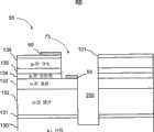
[5]正如Virshup的专利文件以及本申请说明书附图1(该附图1是Virshup的专利文件图2的再现)中所描述的,典型的半导体光功率转换器含有p-n结20,所述p-n结20形成于基极层16和发射极层18之间,所述基极层16可以是典型的n极层,所述发射极层18可以是典型的p极层。所述基极层16和发射极层18被夹在被置于绝缘衬底12上的高导电性缓冲层14和高导电性光学透窗层22之间,在所述光学透窗层22之后可以加上较厚的导电层24。保护层(图1未显示)位于透窗层上,并且如金属栅格线的电接触头(图1未显示)被沉积在所述保护层上。在所述金属栅格线间(典型的如3微米窄的栅格线)蚀刻去除保护层,使得入射光可以穿过透窗层并被下面的p-n结20吸收。为了完成电路,一般还要通过蚀刻技术腐蚀到p-n结的n区。蚀刻深度通常为几微米以确保到达基极层16。一旦当金属被沉积在暴露出来的n极层时,便可以在n极和p极之间建立连接。当光子入射并被p-n结20吸收时,产生载流子,并且在p-n结产生电场的条件下,所述载流子迁移并在电接触器处被收集以在其间产生电势差。通过连接外部电路,便可提取电功率。[5] As described in Virshup's patent document and accompanying drawing 1 of this application specification (the accompanying drawing 1 is the reproduction of Virshup's patent document Fig. 2), a typical semiconductor optical power converter contains a p-n junction 20, and the p-n A junction 20 is formed between a base layer 16, which may be a typical n-pole layer, and an emitter layer 18, which may be a typical p-pole layer. The base layer 16 and the emitter layer 18 are sandwiched between the highly conductive buffer layer 14 and the highly conductive optically transparent window layer 22 disposed on the insulating substrate 12, behind the optically transparent window layer 22 A thicker conductive layer 24 may be added. A protective layer (not shown in FIG. 1 ) is located on the window layer, and electrical contacts (not shown in FIG. 1 ), such as metal grid lines, are deposited on the protective layer. The protection layer is removed by etching between the metal grid lines (typically such as 3 micron narrow grid lines), so that the incident light can pass through the window layer and be absorbed by the p-n junction 20 below. In order to complete the circuit, the n region of the p-n junction is generally etched by etching technology. The etch depth is typically a few micrometers to ensure reaching the base layer 16 . Once the metal is deposited on the exposed n-pole layer, a connection between the n-pole and p-pole can be established. When photons are incident and absorbed by the p-n junction 20, carriers are generated, and under the condition that the p-n junction generates an electric field, the carriers migrate and are collected at the electrical contacts to generate a potential difference therebetween. By connecting an external circuit, electric power can be extracted.
[6]单个p-n结可以传送的开路电压受限于所采用的半导体材料的禁带,并且所述可传送电压一般小于1伏。通过以横向结构的形式将多个所述的p-n结串联,各个电压被累加便可以产生达到或超过12伏的输出电压。为了制作这类单个p-n结元件,一般在相邻分块间进行蚀刻。所述蚀刻必须足够深以使这些p-n结彼此隔离,典型的深度为约25微米。为了完成p-n结的串联,在相邻p-n结之间形成空气桥。所述空气桥的一边接到p-n结的被暴露的n区,另一边接到相邻的p-n结的p区。[6] The open-circuit voltage that can be transmitted by a single p-n junction is limited by the forbidden band of the semiconductor material used, and the transmissible voltage is generally less than 1 volt. By connecting multiple p-n junctions in series in the form of a lateral structure, the respective voltages can be accumulated to generate an output voltage reaching or exceeding 12 volts. To fabricate such individual p-n junction elements, etching is generally performed between adjacent blocks. The etch must be deep enough to isolate these p-n junctions from each other, a typical depth is about 25 microns. To complete the series connection of p-n junctions, air bridges are formed between adjacent p-n junctions. One side of the air bridge is connected to the exposed n region of the p-n junction, and the other side is connected to the p region of the adjacent p-n junction.
[7]对于光功率通过带有圆截面的受限光束传输的应用,如光功率由光纤发出,如图2(该图2是Virshup专利文件图3的再现)所示,这些多个p-n结元件一般通过将半导体芯片的圆形感光区域划分成多个扇形装置分块28来制作,所述分块28通过蚀刻槽26而彼此隔离,并通过互连桥40串联连接;虽然图中显示了6个分块,但是典型的装置可以具有2-16个或更多个分块。[7] For applications where optical power is transmitted through a confined beam with a circular cross-section, such as optical power emitted by an optical fiber, as shown in Figure 2 (this Figure 2 is a reproduction of Figure 3 of the Virshup patent document), these multiple p-n junctions The element is generally fabricated by dividing the circular photosensitive area of a semiconductor chip into a plurality of sector-
发明内容Contents of the invention
[10]本发明的目的之一在于至少克服现有技术中的一些缺点,而提供改善的光功率转换器,所述改善的光功率转换器具有较低的漏电流,较低的内阻和改善的光转换效率。[10] One of the objects of the present invention is to overcome at least some of the disadvantages of the prior art and provide an improved optical power converter with lower leakage current, lower internal resistance and Improved light conversion efficiency.
[11]本发明的另一个目的是提供一种工作在1.3μm到1.55μm波长范围的有效率的光功率转换器。[11] Another object of the present invention is to provide an efficient optical power converter operating in the wavelength range of 1.3 μm to 1.55 μm.
[12]根据本发明,提供一种光电能量转换器,其包括,半导体材料基底,由所述基底支撑的第一多层结构;所述第一多层结构包括第一导电类型的半导体材料的第一基极层、第二导电类型的半导体材料的第一发射极层和第二导电类型的半导体材料的第一导电层;所述第一基极层位于所述基底之上并具有第一禁带;所述第一发射极层与所述第一基极层相邻,所述第二导电类型与所述第一导电类型相反,从而在所述第一发射极层与所述第一基极层之间形成第一结区域,所述第一发射极层具有等于或大于所述第一禁带的第二禁带;所述第一导电层被设置于所述第一发射极层之上,所述第一导电层具有宽于第一和第二禁带中的任一个的第三禁带。第二导电类型的半导体材料的第一电流阻挡层介于所述基底和所述第一多层结构之间。基极电触头被设置以用于与所述第一基极层电连通,发射极电触头被设置于所述导电层上,用于和所述第一发射极层电连通,从而响应于入射到所述第一发射极层上的所选择波长的辐射而产生对于所述基极电触头的相对电压。[12] According to the present invention, there is provided a photoelectric energy converter, which includes a semiconductor material substrate, a first multilayer structure supported by the substrate; the first multilayer structure includes a semiconductor material of the first conductivity type A first base layer, a first emitter layer of a semiconductor material of a second conductivity type, and a first conductive layer of a semiconductor material of a second conductivity type; the first base layer is located on the substrate and has a first band gap; the first emitter layer is adjacent to the first base layer, and the second conductivity type is opposite to the first conductivity type, so that the first emitter layer and the first A first junction region is formed between the base layers, the first emitter layer has a second forbidden band equal to or greater than the first forbidden band; the first conductive layer is disposed on the first emitter layer Above, the first conductive layer has a third forbidden band wider than either of the first and second forbidden bands. A first current blocking layer of a semiconductor material of a second conductivity type is interposed between the substrate and the first multilayer structure. A base electrical contact is disposed for electrical communication with the first base layer, and an emitter electrical contact is disposed on the conductive layer for electrical communication with the first emitter layer, thereby responding A relative voltage is generated across the base electrical contact upon radiation of the selected wavelength incident on the first emitter layer.
[13]根据本发明的一个方面,所述第一发射极层和所述导电层中的至少一个被掺碳,从而使受主掺杂浓度范围在2×10¹⁸到1×1019cm-3。[13] According to an aspect of the present invention, at least one of the first emitter layer and the conductive layer is doped with carbon so that the acceptor doping concentration ranges from 2×10¹⁸ to 1×1019 cm− 3 .
[14]本发明的光电能量转换器可以进一步包括多个沟槽,所述沟槽延伸通过所述第一多层结构和电流阻挡层,而且进一步部分延伸进入基底,从而形成多个由所述基底支撑的空间上分离的装置分块;每一个所述装置分块包括第一金属触头和第二金属触头,所述第一金属触头用于与装置分块内的第一基极层电连通,所述第一金属触头被设置于所述第一发射极层的开口中的第一基极层上,所述第二金属触头被设置于所述装置分块的导电层之上,用于和所述第一发射极层电连通。提供有多个电互连器,用于将每一个且仅一个第一金属触头电连接到各自相邻的第二金属触头,从而形成串联连接的装置分块链,其中,所述第一金属触头中未连接于任一第二金属触头的一个第一金属触头为基极电触头,所述第二金属触头中未连接于任一第一金属触头的一个第二金属触头为发射极电触头。[14] The photoelectric energy converter of the present invention may further include a plurality of grooves extending through the first multilayer structure and the current blocking layer, and further partly extending into the substrate, thereby forming a plurality of substrate-supported spatially separated device segments; each of said device segments comprising a first metal contact and a second metal contact for contacting a first base within the device segment The layers are electrically connected, the first metal contact is arranged on the first base layer in the opening of the first emitter layer, and the second metal contact is arranged on the conductive layer of the device block above, used for electrical communication with the first emitter layer. A plurality of electrical interconnectors are provided for electrically connecting each and only one first metal contact to a respective adjacent second metal contact, thereby forming a chain of device blocks connected in series, wherein the first A first metal contact that is not connected to any second metal contact in a metal contact is a base electrical contact, and a first metal contact that is not connected to any first metal contact in the second metal contacts The two metal contacts are emitter electrical contacts.
[15]根据本发明的一个方面,所述基底,第一基极层和发射极层中的每一个的半导体材料均为GaAs,所述导电层的半导体材料是AlGaAs和InGaP之中的一种合金。[15] According to one aspect of the present invention, the semiconductor material of each of the substrate, the first base layer and the emitter layer is GaAs, and the semiconductor material of the conductive layer is one of AlGaAs and InGaP alloy.
[16]根据本发明的一个方面,所述基底和电流阻挡层的半导体材料是InP,所述第一基极和发射极层的半导体材料是InGaAs和InGaAsP之中的一种合金,以及所述导电层的半导体材料是InP和InGaAsP之中的一种合金。[16] According to one aspect of the present invention, the semiconductor material of the substrate and the current blocking layer is InP, the semiconductor material of the first base and emitter layer is an alloy among InGaAs and InGaAsP, and the The semiconductor material of the conductive layer is an alloy among InP and InGaAsP.
[17]在本发明的一个实施例中,所述基底的半导体材料是掺杂水平小于1015cm-3的具有大致本征电导的GaAs;所述电流阻挡层包括p掺杂GaAs,所述p掺杂GaAs的受主掺杂浓度范围在5 x 10¹⁷到1 x 1019cm-3,厚度范围是0.1到0.3μm;所述缓冲层包括n掺杂GaAsp,所述n掺杂GaAs的施主掺杂浓度范围在5 x 10¹⁷到2 x 1018cm-3,厚度范围是1到10μm;所述第一基极层包括GaAs和铝掺杂浓度不超过35%的AlGaAs合金中的一种,其施主掺杂浓度的范围是5 x 10¹⁷到1 x 1019cm-3,厚度范围是1到3μm;所述第一发射极层包括GaAs和铝掺杂浓度不超过35%的AlGaAs合金中的一种的碳掺杂层,其厚度范围是0.6到1μm,受主掺杂浓度范围在2 x 10¹⁸到5 x 1018cm-3;以及,所述导电层为p型,包括以下的其中一个:Zn或Be掺杂InGaAsP,和铝掺杂浓度不超过35%的碳掺杂AlGaAs,以及所述导电层具有的禁带宽于所述第一发射极和基极层的禁带,厚度范围是1到3μm,施主掺杂浓度范围是2 x 10¹⁸到2 x 1019cm-3。[17] In one embodiment of the present invention, the semiconductor material of the substrate is GaAs with a doping level less than 1015 cm-3 and has approximately intrinsic conductivity; the current blocking layer includes p-doped GaAs, and the The acceptor doping concentration of p-doped GaAs ranges from 5 x 10¹⁷ to 1 x 1019 cm-3 , and the thickness ranges from 0.1 to 0.3 μm; the buffer layer includes n-doped GaAsp, and the n-doped GaAs The donor doping concentration ranges from 5 x 10¹⁷ to 2 x 1018 cm-3 , and the thickness ranges from 1 to 10 μm; the first base layer includes one of GaAs and an AlGaAs alloy whose aluminum doping concentration does not exceed 35%. species, the donor doping concentration ranges from 5 x 10¹⁷ to 1 x 1019 cm-3 , and the thickness ranges from 1 to 3 μm; the first emitter layer includes GaAs and AlGaAs whose aluminum doping concentration does not exceed 35% A carbon-doped layer of one of the alloys, the thickness of which is in the range of 0.6 to 1 μm, and the acceptor doping concentration in the range of 2 x 10¹⁸ to 5 x 1018 cm-3 ; and, the conductive layer is p-type, comprising One of the following: Zn or Be-doped InGaAsP, and carbon-doped AlGaAs with an aluminum doping concentration not exceeding 35%, and the conductive layer has a band gap higher than that of the first emitter and base layers , the thickness range is 1 to 3 μm, and the donor doping concentration range is 2 x 10¹⁸ to 2 x 1019 cm-3 .
[18]在本发明的另一个具体实施例中,所述基底的半导体材料是半绝缘铟磷酸盐(InP);所述电流阻挡层包括受主掺杂浓度是5 x 1017cm-3或更高的p掺杂InP,厚度范围是0.2到0.3μm;所述缓冲层包括施主掺杂浓度是5 x 1017cm-3或更高的n掺杂InP,厚度范围是5到10μm;所述第一基极层包括与InP晶格匹配的InGaAs合金,其施主掺杂浓度是5 x 1017cm-3或更高,厚度范围是1到3μm;所述第一发射极层包括与InP晶格匹配的p掺杂InGaAs合金,其受主掺杂浓度是2 x 1018cm-3或更高,厚度范围是0.5到1.5μm;以及,所述导电层包括施主掺杂浓度是2 x 1018cm-3或更高的p掺杂InP,其厚度范围是1.5到2.5μm。[18] In another specific embodiment of the present invention, the semiconductor material of the substrate is semi-insulating indium phosphate (InP); the current blocking layer includes an acceptor doping concentration of 5 x 1017 cm-3 or Higher p-doped InP with a thickness in the range of 0.2 to 0.3 μm; the buffer layer including n-doped InP with a donor doping concentration of 5 x 1017 cm-3 or higher with a thickness in the range of 5 to 10 μm; The first base layer includes an InGaAs alloy lattice-matched with InP, its donor doping concentration is 5 x 1017 cm-3 or higher, and its thickness ranges from 1 to 3 μm; the first emitter layer includes an InP a lattice-matched p-doped InGaAs alloy having an acceptor doping concentration of 2 x 1018 cm-3 or higher and a thickness in the range of 0.5 to 1.5 μm; and, said conductive layer including a donor doping concentration of 2 x 1018 cm-3 or higher p-doped InP with a thickness ranging from 1.5 to 2.5 μm.
附图说明Description of drawings
[19]下面将结合代表本发明优选实施例的附图更详细的描述本发明,其中,相同的参考标识用于指示相同的器件,其中:[19] The invention will be described in more detail below with reference to the accompanying drawings representing preferred embodiments of the invention, wherein the same reference numerals are used to designate the same components, wherein:
[20]图1是现有技术下的半导体光能量转换器的层结构示意图;[20] Figure 1 is a schematic diagram of the layer structure of a semiconductor light energy converter in the prior art;
[21]图2是现有技术下的分块式半导体光能量转换器的平面图;[21] Figure 2 is a plan view of a block-type semiconductor light energy converter in the prior art;
[22]图3是根据本发明的一个实施例的光电能量转换器的平面图,所述光电能量转换器含有中心部分;[22] FIG. 3 is a plan view of a photoelectric energy converter according to an embodiment of the present invention, the photoelectric energy converter having a central part;
[23]图4是图3所示的光电能量转换器的沿A-A线的截面图,以说明其示例性层结构;[23] Fig. 4 is a cross-sectional view along line A-A of the photoelectric energy converter shown in Fig. 3 to illustrate its exemplary layer structure;
[24]图5是图3和图4所示的光电能量转换器的沿图3中B-B线的截面图;[24] Fig. 5 is a cross-sectional view along line B-B in Fig. 3 of the photoelectric energy converter shown in Fig. 3 and Fig. 4;
[25]图6是根据本发明的一个实施例的光电能量转换器的平面图,所述光电能量转换器含有独立可寻址中心部分;[25] FIG. 6 is a plan view of an optoelectronic energy converter having an individually addressable central portion according to one embodiment of the present invention;
[26]图7是图6所示光电能量转换器的一个示例性实施例的沿图6中C-C线和D-D线的截面图;[26] Fig. 7 is a cross-sectional view along line C-C and line D-D in Fig. 6 of an exemplary embodiment of the photoelectric energy converter shown in Fig. 6;
[27]图8是图6所示光电能量转换器的另一可选实施例的沿图6中C-C线和D-D线的截面图;[27] Fig. 8 is a cross-sectional view along line C-C and line D-D in Fig. 6 of another optional embodiment of the photoelectric energy converter shown in Fig. 6;
[28]图9是根据本发明的GaAs/AlGaAs光电能量转换器在50mW光照条件下的电流-电压(I-V)特性和输出功率-电压(P-V)特性的曲线示意图;[28] FIG. 9 is a schematic diagram of the current-voltage (I-V) characteristics and output power-voltage (P-V) characteristics of the GaAs/AlGaAs photoelectric energy converter according to the present invention under 50mW illumination conditions;
[29]图10是根据本发明的InGaAs/InP光电能量转换器在波长1430nm,强度100mW的光照条件下的电流-电压(I-V)特性和输出功率-电压(P-V)特性的曲线示意图。[29] FIG. 10 is a schematic diagram of the current-voltage (I-V) characteristics and output power-voltage (P-V) characteristics of the InGaAs/InP photoelectric energy converter according to the present invention under the light conditions of a wavelength of 1430nm and an intensity of 100mW.
具体实施方式Detailed ways
[30]下面首先参照图3、4和5对本发明的光电能量转换器(PPC)的示范实施例进行描述。[30] An exemplary embodiment of a photoelectric power converter (PPC) of the present invention will first be described below with reference to FIGS. 3 , 4 and 5 .
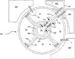
[31]首先参见图3,PPC 50含有多个装置分块51-55,所述分块以圆形组合方式排列,其具有中心部分或中心分块55和多个设置在所述中心分块55周围的分块51-54,所述多个分块围绕所述中心分块55而形成环状结构。分块51-54以及中心分块55通过窄沟槽100和200而彼此隔离,各分块51-54在此又被称为环状分块。环形或通常为无间断的沟槽200将中心分块55与其他环状分块51-54隔离,而沟槽100从沟槽200处径向延伸并将各环状分块51-54彼此隔离。沟槽100和200在外延生长的半导体晶片内采用蚀刻技术领域中已知的具有高纵横比的方法进行蚀刻,所述具有高纵横比的蚀刻方法例如反应式离子蚀刻法(RIE)。电互连器70在接触垫61和62之间将分块51-55串联,电互连器70将以空气桥的形式在下文中进一步详细描述,以使所述装置被适当波长的光照射时每个分块上可以产生电压,从而每个分块上产生的电压被累加,以在接触垫61和62之间产生分别较高的输出电压Vout。虽然图3中所示的PPC50只有四个环状分块,但其他实施例中含有的环状分块可以低于或可以高于图3中所示环状分块的数量,以便提供较高的输出电压。通常,基于较低能隙材料的装置将需要更多的装置分块以实现例如6V的所期望的输出电压值Vout。例如,下文中描述的InP基装置可能具有12个或更多个装置分块,而GaAs基装置可能适合于配置5个装置分块。[31] Referring first to Figure 3, the
[32]图4是图3中所示PPC 50的沿“A-A”线的部分截面图,用以说明PPC 50的层结构;所述层结构包括一个半绝缘或绝缘基底130,第一电流阻挡层131,以及第一多层结构30,所述第一多层结构30依次包括第一半导体材料的第一电导类型的缓冲层132,具有第一能隙的第一半导体材料的第一电导类型的第一基极层133,具有第二能隙的第二半导体材料的与所述第一电导类型相反的第二电导类型(以在其间形成p-n结区域129)的第一发射极层134,以及第三半导体材料的第二电导类型的导电层136。所述第一和第二半导体材料用于吸收入射光并在发射极层和基极层产生少数光诱导载流子,然后通过p-n结区域129的电场将所述光诱导载流子吸入邻近的发射极层或基极层,在所述邻近的发射极层或基极层内少数载流子成为多数载流子并且为所述第一发射极层134和基极层133充电,所述第一发射极层134和基极层133将在下文中被称为第一活性层,其具有相反极性的电荷从而产生光诱导电压。导电层136的第三半导体材料对入射光是透明的并且含有第三禁带,所述第三禁带宽于形成第一基极层133的第一半导体材料和形成第一发射极层134的第二半导体材料中的任何一种材料的禁带。可选地,对入射光透明的第二导电类型的接触层或保护层101可被沉积于导电层136上方,以便有助于与第一金属触头60和栅格线(未在图中示出)形成较好的欧姆接触。所述术语“禁带(bandgap)”和“能隙(energy bandgap)”在本申请中可互换使用,指半导体材料中价带顶部和导带底部之间的能量差异。[32] FIG. 4 is a partial cross-sectional view along the "A-A" line of the
[33]位于基极层133下方的缓冲层132相对厚于基极层133和发射极层134。在操作中,缓冲层132起到第二导电层的作用以有助于所述第一极的光生载流子移动至各自的第一金属触头65;缓冲层132具有低表面电阻,优选小于1欧姆/cm2。基底130和第一电流阻挡层131可以采用第一半导体材料,即与缓冲层132和第一基极层133的材料相同,以有助于具有低缺陷密度的高品质基极层133的外延生长,所述缺陷将造成光诱导载流子的非辐射复合。所述第二半导体材料,即所述第一发射极层的材料优选采用与所述第一半导体材料相同或高于其的禁带并且实际上与所述第一半导体材料具有相同的晶格常数。[33] The
[34]基底130应该具有高电阻系数以便阻止缓冲层132中流动的光生载流子穿过基底130而渗漏,所述载流子的渗漏将减少PPC 50的输出电压并且因此降低PPC 50的性能。因为未掺杂质且具有本征导电性的最适合的半导体材料制成的高品质基底仅是半绝缘性的,所以,基底130可以是由所述第一半导体材料制成的固有绝缘或半绝缘基底,所述第一导体材料优选具有不小于107欧姆/厘米的电阻率。对于基底的选择,优选未掺杂质GaAs或InP基底,所述GaAs或InP基底的本底掺杂不超过1015cm-3。这样的本底掺杂将确保基底内没有直流传导,但是不能阻止基底内不希望出现的光诱导电流传导。[34] The
[35]有利之处在于,根据本发明,第一电流阻挡层131被插入在半绝缘层基底130和缓冲层132之间,第一电流阻挡层131具有与缓冲层132的第一电导类型相反的第二电导类型,并因此与缓冲层132形成一个p-n结127,所述p-n结127阻止缓冲层132的多数载流子流入基底130,以便进一步抑制所述装置的分块之间通过基底130的渗漏电流。位于电流阻挡层131和缓冲层132之间的p-n结127在下文被称为电流阻挡结127或第一电流阻挡结。[35] Advantageously, according to the present invention, the first
[36]尽管在根据本发明的其他实施例中第一电导类型可以是p型电导,而第二电导类型是n型电导,但是在此所述的实施例中的第一电导类型是n型电导,而第二电导类型是p型电导。所述n型是指掺有掺杂材料或提供施主杂质的的半导体材料的电导,所述半导体材料中的大多数载流子为电子;所述p型是指掺有掺杂材料或提供受主杂质的半导体材料的电导,所述半导体材料中的大多数载流子为空穴。当术语“n(p)-型”和“n(p)-掺杂”指半导体材料的各自电导类型时,在此可以互换使用。下文中所使用的“掺杂级”指n型半导体材料中施主杂质的净浓度,或指p型半导体材料中受主杂质的净浓度。[36] Although in other embodiments according to the present invention the first conductance type may be p-type conductance and the second conductance type is n-type conductance, in the embodiments described herein the first conductance type is n-type conductance, and the second conductance type is p-type conductance. The n-type refers to the conductance of a semiconductor material doped with doping materials or providing donor impurities, and the majority of carriers in the semiconductor material are electrons; the p-type refers to doping with doping materials or providing donor impurities. The conductance of a semiconductor material where the majority of charge carriers are holes as the main impurity. The terms "n(p)-type" and "n(p)-doped" are used interchangeably herein when referring to the respective conductivity types of semiconductor materials. The "doping level" used hereinafter refers to the net concentration of donor impurities in n-type semiconductor materials, or the net concentration of acceptor impurities in p-type semiconductor materials.
[37]所述第一基极层可以掺有浓度范围在5×1017cm-3至1×1019cm-3的施主杂质。所述第一基极层可以掺有浓度高于5×1017cm-3的受主杂质,或优选掺有浓度范围在2×10¹⁸至1×1019cm-3的受主杂质,或最优选为掺有浓度范围在3×10¹⁸至5×1018cm-3的受主杂质。在其他实施例中,所述第一基极层可以掺有的施主杂质浓度从远离p-n结区域129至电流阻挡层131逐渐增加,其浓度范围从小于2×1017cm-3到至少为2×1018cm-3。类似地,所述发射极层的受主杂质从远离p-n结区域129至导电层136逐渐增加,其浓度水平从小于2×1017cm-3到至少为2×1018cm-3。[37] The first base layer may be doped with donor impurities at a concentration ranging from 5×1017 cm−3 to 1×1019 cm−3 . The first base layer may be doped with acceptor impurities at a concentration higher than 5×1017 cm−3 , or preferably doped with acceptor impurities at a concentration ranging from 2×10¹⁸ to 1×1019 cm−3 , or Most preferably, it is doped with acceptor impurities at a concentration ranging from 3×10¹⁸ to 5×1018 cm−3 . In other embodiments, the first base layer can be doped with a donor impurity concentration that gradually increases from away from the pn junction region 129 to the
[38]在第一优选实施例中,基底130、电流阻挡层131、缓冲层132、第一基极层133以及第一发射极层134的半导体材料采用砷化镓(GaAs),导电层136和可选透窗层135的半导体材料采用InGaP和AlGaAs中的一种或两者,以及所述可选保护层的半导体材料采用砷化镓(GaAs)。[38] In the first preferred embodiment, the semiconductor material of the
[39]更具体的,基底30由实质上不掺杂的GaAs所形成,基底30的本底掺杂级不超过1015cm-3并且可以具有几百微米的厚度,例如厚度范围在350微米至650微米之间。电流阻挡层131在基底30上外延生长,并且电流阻挡层131的半导体材料是p-型GaAs,所述p-型GaAs的受主杂质浓度范围在5×1017cm-3至1×1019cm-3之间,或者例如浓度大约是2×1018cm-3,并且厚度范围在0.2至0.3微米之间例如0.25微米。缓冲层132外延生长于电流阻挡层131上,所述缓冲层132的半导体材料是n型高掺杂GaAs,并且所述n型高掺杂GaAs的施主浓度范围在5×1017cm-3至2×1018cm-3之间,并且厚度范围在1至10微米之间,例如5微米。第一基极层133外延生长于缓冲层132上,所述第一基极层133的半导体材料也是n型GaAs,所述n型GaAs的施主浓度范围在5×1017cm-3至2×1018cm-3之间例如1×1018cm-3,并且厚度范围大约为3微米。第一发射极层134外延生长于第一基极层133上,并且所述第一发射极层134的半导体材料是p型GaAs,所述p型GaAs的受主杂质浓度范围在2×1018cm-3至1×1019cm-3之间,优选在3×1018cm-3至5×1018cm-3之间,并且厚度范围在0.2至1微米之间,例如0.8微米。所述p-n结区域129形成于第一基极层133和第一发射极层134之间。[39] More specifically, the
[40]可选透窗层135外延生长于第一发射极层134上,并且所述可选透窗层135的半导体材料是GaAs的第一合金,例如AlGaAs或更具体的是AlxGa1-xAs,所述AlxGa1-xAs合金中铝的相对含量x>50%,例如x=80%。可选透窗层135具有与第一发射极层134相同的或更高的p型电导。之所以选用AlGaAs是因为其对于PPC 50工作的所选辐射波长的光透率,以及由于第一发射极层134的钝化,从而减少第一发射极层134与其后层的界面上的光诱导载流子的非辐射复合率。可选透窗层135的受主杂质浓度可以为5×1018cm-3并且其厚度范围可以在0.02至0.1微米之间,例如0.08微米。[40] The optional
[41]导电层136可以高掺杂浓度的p极层,所述高掺杂浓度的p极层的受主杂质浓度范围在2×1018cm-3至2×1019cm-3之间,并且优选为3×1018cm-3或者更高,以降低导电层136的表面阻抗。导电层136的半导体材料可以是AlGaAs的第二合金,例如AlxGa1-xAs,所述AlxGa1-xAs中铝的相对含量少于50%,,例如20%,并且其厚度范围在1至3微米之间,例如2微米。导电层136的AlGaAs的第二合金中的铝含量x应该足够高,以确保导电层136对于所选波长的入射辐射的光透率。另一方面,减少所述导电层的所述铝含量有利于降低其表面阻抗,因为减少了所述导电层的不希望出现的氧化。[41] The
[42]因此,根据本发明的一个可选实施例,利用不含铝的导电层136,例如InGaP合金的p-掺杂层,所述InGaP合金例如是InxGa1-xP的合成材料,其中x的范围在0.5至0.54之间。所述层可以在铝含量超过50%的AlGaAs第一合金的可选透窗层135上外延生长,或可以直接在p-掺杂GaAs的第一发射极层134上外延生长。[42] Therefore, according to an alternative embodiment of the present invention, a
[43]本发明的另一方面涉及将碳(C)用作优选的掺杂材料,所述碳(C)掺杂材料用于本发明的优选实施例的PPC 50的p-掺杂层,所述p-掺杂层如电流阻挡层131、第一发射极层134、可选透窗层135以及导电层136,所述碳(C)掺杂材料用以代替较为传统的p-掺杂材料如铍(Be)和锌(Zn),所述铍(Be)和锌(Zn)一般用于GaAs基和InP基光电设备。有利的是,所述碳(C)掺杂材料的使用可以加强p-掺杂第一发射极层134中和跨越p-n结区域129的电场强度以及增加所述PPC的内部量子效率。传统掺杂剂,如锌,在大于5×1017cm-3的高掺杂级时可能出现有害的效应,如少数载流子的寿命降低,然而所述碳(C)掺杂将不会产生所述有害效应,或者至少将有害效应大大减小。所述碳(C)掺杂使得高度掺杂GaAs或InGaAs的半导体材料可以很好地保持少数载流子的寿命并且因此有助于活性层133/134实现高量子效率,即高比例光生电子和空穴在无非辐射复合情况下离开所述p-n结区域129。因此,将碳作为掺杂材料,第一发射极层134的p-掺杂级可以在大体上没有降低所述装置的量子效率条件下达到5×1018cm-3。与之相反,采用如锌的传统掺杂材料在高掺杂级,如大于2×1018cm-3时,p-n结区域129的p极层将产生额外的非辐射复合中心并且降低少数载流子寿命,从而导致量子效率的降低并且导致所述PPC所产生的光电流和/或输出电压变小。此外,半导体宿主材料中的碳离子空间分布较传统受主杂质如Zn和Be更具稳定性。通过这种稳定性,碳掺杂可以在所述p-n结区域129的p极部分和n极部分之间形成更陡的高梯度界面,有助于使p-n结获得更强的电场并且使得从p-n结内迁移出的光生少数载流子的迁移率更高,有利于产生光生电流。导电层136的所述碳掺杂可以通过提供具有高掺杂级的较高品质材料以降低导电层136的表面阻抗,尤其是所述较高品质材料与所述导电层136中含有较少铝的InGaP材料结合使用时更有利于降低所述表面阻抗。[43] Another aspect of the present invention relates to the use of carbon (C) as the preferred doping material for the p-doped layer of the
[44]上述实施例是直接将光转变成电功率,所述光波长范围在0.8至0.9微米之间,通过所述导电层的GaAs的禁带和AlGaAs/InGaP的禁带所详细说明,其中所述基极层133和所述发射极层134的半导体材料是GaAs。本领域技术人员可以判断出无论短波光或长波光可以通过所述PPC50被转换,所述PPC50通过使用与所述GaAs基底相匹配的AlGaAs或InGaAs合金层栅格作为所述缓冲器132和所述发射极层134,并且适当调整所述导电层136的金属沉积。例如,铝含量x从5%至35%的AlxGa(1-x)As合金可以被用于所述第一活性层133和134,并且其他铝含量较高的AlxGa(1-x)As合金或InGaP合金可以被用于所述导电层136,所述合金相对于所述第一活性层133和134的半导体材料具有更高的禁带。通过在GaAs基底上使用AlGaAs或InGaAs生长制作所述第一活性层133/134,所述PPC 50被制造适用于光波长范围大约从0.7微米到大约1.3微米。所述导电层136的禁带可以在0.15eV和0.5eV(电子伏特)之间,高于所述发射极层134的禁带,以便确保所述导电层136用于被所述第一活性层133/134层所吸收的入射光的光透率。[44] The above embodiment directly converts light into electric power, and the wavelength range of the light is between 0.8 and 0.9 microns, and is specified by the forbidden band of GaAs and AlGaAs/InGaP of the conductive layer, wherein the The semiconductor material of the
[45]所述PPC 50的其他实施例使用层结构,所述层结构在磷酸铟(InP)基底上外延生长,并且所述PPC 50适用于转换波长范围在1.2微米至1.6微米之间的光,大多数商业光纤在所述波长范围内都具有低光损。例如,所述其他实施例中一例,所述PPC50可以在其层结构里使用下述半导体材料。所述基底130的半导体材料是半绝缘体InP,所述半绝缘体InP掺有含量为1016cm-3的铁(Fe)杂质并且具有107ohm/cm的高电阻系数。所述电流阻塞层131是掺有杂质的p型InP层,所述p极层的厚度范围在0.2微米至0.3微米之间,例如0.25微米,并且掺杂级为5×1017cm-3或更高;所述缓冲层132是掺有InP杂质的n极层,所述n极层的厚度范围在5微米至10微米之间,例如7微米,并且掺杂级为5×1017cm-3或更高;所述第一基极层133的半导体材料是n极InGaAs合金层,所述InGaAs合金层与InP层晶格匹配并且其厚度范围在1微米至3微米,例如3微米,并且施主杂质浓度为5×1017cm-3或更高;所述第一发射极层134是p极InGaAs合金层,所述InGaAs合金层与InP层晶格匹配并且其厚度范围在0.5微米至1.5微米,例如1微米,并且受主杂质浓度范围为2×1018cm-3至1×1019cm-3之间或者优选范围在3×1018cm-3至5×1018cm-3之间并将碳杂质作为优选掺杂材料;所述导电层136是掺有InP杂质的p极层,所述p极层的厚度范围在1.5微米至2.5微米之间,例如2微米,并且受主杂质浓度范围在2×1018cm-3至2×1019cm-3之间,并且优选浓度范围超过3×1018cm-3。例如,p极InP层131和136的掺杂材料可以是Be。所述接触层101的半导体材料是p极InGaAs合金层,优选碳杂质作为掺杂材料,并且掺杂级大约为2×1018cm-3或更高,并且所述p极层的厚度范围在0.1微米至0.2微米之间。[45] Other embodiments of the
[46]参见图3,所述PPC50的所述装置分块51-55通过前述层结构的PPC晶片通过形成的所述沟槽100和200制造,所述沟槽100和200延伸超过所述第一多层结构30和所述电流阻塞层131,并且部分延伸进入所述基底130,以使所述装置分块51-55之间电隔离和空间隔离并且所述装置分块51-55通过所述基底支撑,所述基底至少是半绝缘体,即含有的电阻系数不超过107ohm/cm,以便与所述电流阻塞层131共同作用以减少所述装置分块间的渗漏电流。[46] Referring to FIG. 3, the device segments 51-55 of the
[47]所述沟槽的深度根据所述第一多层结构30的总厚度确定,并且范围可以在10微米至20微米之间。所述沟槽100和200的纵横比应当适当提高以使入射光纤的分段最小化,所述入射光纤的分段到达所述基底材料,所述基底材料位于所述沟槽的底部,所述纵横比通过沟槽深575与沟槽宽573的比例确定,所述沟槽深和沟槽宽分别用“箭头”标注于图4中,由于所述光将在所述基底材料处被吸收并产生光载流子并因此造成所述基底材料电导系数不必要的增加,从而在所述装置分块间造成潜在的电导路径,所述电导路径将导致所述PPC装置光转换率的降低。因此,所述沟槽100和200应当适当窄,并优选所述沟槽宽范围在2微米至10微米之间,例如5微米或更小,并且所述沟槽100和200的纵横比应当大于4且优选大于5。所述电流阻塞层131阻止所述缓冲层132内的多数载流子从其流向所述基底,因此所述电流阻塞层131将阻止所述装置分块间的渗漏电流通过所述基底130,将使所述PPC 50装置的光转换率相对于不含所述电流阻塞层131的相似装置的光转换率获得惊人的提高。所述术语“光转换率和功率转换率”在这可交替使用,两者都定义为由所述PPC装置提供给外电路的电功率与所述PPC装置的入射光的光功率的比值。[47] The depth of the groove is determined according to the total thickness of the
[48]在所述装置分块51-55的每一块分块中,第一金属触头65沉积在所述第一基极层133上用于与所述第一基极层的电连通,并且第二金属触头60沉积在所述可选保护层101上或在没有所述可选保护层时直接沉积在所述导电层136上用于与所述第一发射层134的电连通。然后电互连器70以金属空气桥的形式将每个所述第一金属触头65与邻近设备分块的所述第二金属触头进行连接但是每个空气桥只连接一个所述第一金属触头和一个邻近的所述第二金属触头,以使所有的所述装置分块51-55实现串联。当经过选择的光投射到所述PPC 50上时,加入电压用以在所述第一金属触头和所述第二金属触头处产生更高的总输出电压Vout,所述经过选择的光通过所述第一活性层133/134的吸收范围和所述导电层136的传输范围选择,所述电压产生于所述装置分块51-55的每一块分块的p-n结区域129,所述第一金属触头和所述第二金属触头不与任何其他的第一和第二金属触头保持连接。这些不与任何其他的第一和第二金属触头保持连接的所述第一金属触头和所述第二金属触头在此分别作为基极和发射极的电触头;所述触头可以通过空气桥71连接至接触垫61和62以便连接到所述PPC 50的外电路。[48] In each of said device segments 51-55, a
[49]如图3所示的实施例,所述装置分块51的所述第二金属触头60可以通过空气桥70连接到所述装置分块52的所述第一金属触头65,所述触点截面如图4所示。所述装置分块51的所述第二金属触头60可以通过空气桥70连接到所述装置中心分块55的所述第一金属触头65,所述装置中心分块55的所述第二金属触头60通过空气桥连接到所述装置分块53的所述第一金属触头65。所述装置中心分块55的所述第一金属触头65和所述第二金属触头60都具有环状结构并且涉及下文中的所述第一和第二触头。所述中心触头60和65环绕所述中心分块55设置,所述中心分块55的所述第一环状触头65邻近环状沟槽200并且所述第二环状触头60位于所述中心分块55内且紧邻所述第一环状触头65,如图5所示所述第一环状触头65位于开口73内,图5是用于说明光电能量转换器的层结构的截面图,所述层结构是沿着图3中所示划线B-B的截面图。所述第一环状触头65处有一开口61,空气桥70通过所述开口61将所述第二环状触头60连接至邻近设备分块的所述第一金属触头65处,所述第二金属触头通过另一个空气桥70连接至所述最后的装置分块54的所述第一金属触头。这种交互连接结构导致各所述装置分块51、52、53、54和55以一定的顺序串联,所述的串联方式获得在所述发射极电触头和基极层电触头之间的输出电压Vout,即在所述装置分块54的所述第二金属触头和所述装置分块51的所述第二金属触头60之间产生输出电压,所述输出电压接近于所述装置分块51-55每个分块p-n结处产生电压的总值。所述装置分块54和51通过空气桥71保持与所述金属接触垫61(如图3所示)和62的金属连接,所述金属接触垫61和62分别作为所述PPC 50的阳极和阴极。[49] In the embodiment shown in FIG. 3, the
[50]所述第一和第二金属接触电65和60可以在单个金属镀层工序中沉积,所述金属镀层工序完成后进行触头结构制作工序和空气桥70和71制作,如Virshup专利中所描述的。所述装置分块51-54的外部更适于进行所述第二环状触头60沉积,以便与所述保护层101上的金属栅格线相重叠,而所述中心分块55没有任何金属栅格线并且各分块相应的所述第二环形触头60直接在所述接触保护层101上沉淀。所述中心分块55的所述第一和第二环形触头65和60的宽度应该适当的窄以便将所述中心分块55的所述接触保护层101表面的大部分区域留给入射光。经由实施例可知,所述环形分块51-54的外围圆周直径为1800微米,所述中心分块的圆周直径为250微米,以及所述环状触头65和60的宽度范围在10微米到50微米之间。[50] The first and
[51]先沉积所述第一金属触头64,位于各装置分块中的所述第一基极层133在各装置分块的选定位置暴露出来,优选接近沟槽,所述沟槽可以将所述第一基极层133与邻近装置区域隔离,通过可选择蚀刻法,从所述多层结构30的顶部蚀刻至所述第一基极层133的上方以便在形成开口73,并在所述第一发射极层134中沉积所述第一金属触头65,如图4所示,图4是用于说明图3中所示光电能量转换器的层结构的截面图,所述层结构是沿着图3中所示划线A-A的截面图。[51] Deposit the first metal contact 64 first, and the
[52]本发明中所述PPC50的装置分块布局具有新颖的技术特征,与图1中现有技术下的“扇形楔”相比有利于提供更高的光功率转换效率,在本发明所述装置分块布局中装置分块55位于中心处并由一组装置分块51-54环绕,所述装置分块51-54在中心分块55周围沉淀,图1的现有技术中所述沟槽26全部会聚于所述PPC的中心以在所述装置感光表面的中心有效的形成一个空心。所述现有技术严重的影响现有技术条件下的光能量转换器的转换效率,其中入射光以光束的形式进入,所述光束的密度从光束轴向外递减,例如从单模光纤中发出的高斯或类似于高斯的光束。之处在于,本发明所述PPC 50消除现有技术装置中的缺陷,通过利用位于装置中心的分块55,所述分块55可以利用入射光束中心的光,所述入射中心的光强最大。根据入射光密度分布对所述PPC进行几何处理,不均运照射布局产生的消极影响被极大的避免。我们发现,通过采用适当尺寸的中心装置分块55,所述PPC 50的光转换效率提高了25%,所述PPC 50中含有5个分块。我们又发现,为了将高斯光束的光功率有效地转换为电功率,所述中心分块55所具有的感光表面的面积与所述PPC 50所具有的感光表面的总面积的比例优选在15%和25%之间,更为优选的是20%。然而,在申请中所述入射光强在所述PPC 50的感光表面实际上是相同的,所述分块51-54的感光表面的面积是相等的。注意术语“感光表面”用于定义入射光到达所述活性层所穿过的所述PPC的表面,所述活性层用于吸收入射光并将其转换成电流。PPC 50的感光表面是所有装置分块51-55接受光的总面积的一部分,如图3所示,所述感光表面未被金属覆盖。术语“感光表面”在此用于定义各分块的感光表面。另一个有利之处在于,所述中心分块55使得装置中非必须的电压降减少并且与阻抗路径一起连接到所述接触垫61和62,所述阻抗路径是载流子在装置中产生并传导的路径。通过中心分块捕获的光,电流不需要通过阻抗材料的长距离传输,但是可以直接在邻近中心分块处被收集并通过金属栅格线传输,所述金属栅格线相对于装置的周长具有低的阻抗。在现有技术中,没有利用装置中心部分收集电流的方法。[52] The block layout of the PPC50 device in the present invention has novel technical features, which is beneficial to provide higher optical power conversion efficiency compared with the prior art "sector wedge" in Fig. 1, in the present invention The plant block layout described has
[53]参见图6,根据本发明的另一个实施例提供的PPC 150,其中所述中心分块55独立于环形分块51-54进行连接并且与其电隔绝。本实施例中所述PPC 150具有4个端口,包括作为第一装置部分的中心装置分块55,所述分块与作为第二装置部分的环形分块51-54相互电隔绝,并且所述第一装置部分可以独立电连接。所述环形分块51-54在接接触垫261和262间串联,以形成所述PPC 150中的环形装置部分简称环形部分。注意图3-7中,相同的数字用于表示相同的元件以简化说明并且有助于理解实施例,只是,中心分块55的第一和第二环形触头在本实施例中分别被标为109和108,以将其与环形分块51-55的第一和第二金属触头65和60相区别,所述第一和第二金属触头65和60如图4中所示。与PPC 50中的被连接到各自环形分块的第一和第二金属触头不同,所述PPC 150的所述中心装置分块55的所述第一和第二环形触头109和108通过电导路径118和119分别连接至接接触垫263和264,所述电导路径118和119的宽度优选小于15微米,所述电导路径118和119位于邻近沟槽100处,所述沟槽100将所述装置的两个环形分块分隔。所述电导路径118和119被设置在所述装置分块51和54上并且所述装置分块从所述电导路径的内圆周延伸到外圆周,但第二电流阻挡层106使得所述电导路径与所述装置分块绝缘,所述第二电流阻挡层在所述保护层101上外延生长并且所述第二电流阻挡层具有的电导性与所述保护层101的电导性相反。所述电导路径118和119也在这分别被称为第三和第四金属触头。所述第三和第四金属触头跨越所述环形装置部分而向外延伸,并且与所述环形装置部分的装置分块电绝缘,以便独立于所述环形装置部分的装置分块51-54而连接到外电路。[53] Referring to FIG. 6, a
[54]所述第二电流阻挡层如图7所示,所述图7是PPC 150沿划线“C-C”(虚线128左侧)和沿划线“D-D”(虚线128右侧)部分的截面视图。在前述实施例中,基底130和第一活性层133/134的半导体材料是GaAs,导电层136和保护层101的半导体材料是p型,以及第二电流阻挡层106可以是n-掺杂GaAs,所述n-掺杂GaAs的掺杂级至少为5×1017cm-3并且其厚度在范围1至5微米。电导路径119和118可以与第一和第二金属触头65和60在同一金属镀层工序或在不同金属镀层工序中形成,金属镀层工序完成后紧接着进行触头结构制作工序,第二阻挡层106在电导路径119和118形成后被去除,仅保留直接位于所述窄金属电导路径119和118下方的部分。[54] The second current blocking layer is shown in FIG. 7, which is a part of the
[55]接接触垫261和262之间的装置分块51-54通过空气桥70串联,除装置分块51外,每块装置分块51-54的第一金属触头65被连接至下一相邻环状装置分块的第二金属触头60,以使装置分块51-54形成顺序连接链,所述连接链里的第一装置分块51的第一金属触头65通过第一空气桥71连至接接触垫261,并且装置分块54的第二金属触头60通过第二空气桥71连至接接触垫262。接接触垫263和264作为PPC 150的第一部分或中心部分55的阳极和阴极,而接接触垫261和262作为PPC 150的第二部分或环形部分51-54的阳极和阴极,所述环形部分包括顺序连接的环形装置分块51-54。[55] The device sub-blocks 51-54 between the
[56]有利之处在于,PPC 150可以作为结合了PPC和较常规的光电探测器(PD)的集成装置,所述集成装置的PPC部分相应于所述环形部分51-54,所述集成装置的PD部分相应于所述中心部分55。当采用含有适当波长的光照射时,所述光波含有载有数据的调制成分,所述PPC 150可以提供电功率并在终端263和264提供探测数据,所述电功率在装置终端261和262之间为5伏或电压更高的信号形式,用于例如驱动外部电路。此外,所述装置的中心部分55可以采用来自装置阳极终端263和阴极终端264的正向偏压,以驱动其活性层133/134以发射光而非吸收光,因此PPC 150的中心部分55可作为发光二极管(LED)使用,例如用于发射而非探测光数据信号。[56] Advantageously, the
[57]因此,本发明提供一个四端口PPC,其具有两个独立可寻址部分,不同于图1中现有技术的光功率转换器以及本发明的PPC 50实施例,图1中现有技术的光功率转换器以及本发明的PPC 50实施例都是两端口装置。有利之处在于,PPC 150的独立寻址部分可被用于完成两个不同的功能,例如在同一装置中执行光能转换和同时接受或发射光数据。[57] Accordingly, the present invention provides a four-port PPC with two independently addressable sections, unlike the prior art optical power converter in FIG. The optical power converter of the technology and the
[58]如图7中所示实施例,PPC 150的中心部分和环形部分在同一p-n结129中分别采用不同的空间区域探测或发射光,并且将光能转变成电能。然而,所述p-n结129也许并非最适于接受或发射光数据信号,即用于执行所述LED或PD功能。而且,在一些应用中,光数据信号和光能可以通过不同波长的光载送。[58] In the embodiment shown in FIG. 7, the central part and the annular part of the
[59]参见图8,PPC 150的另一个实施例含有第二多层结构32,例如所述结构为p-i-n型,被设置在中心分块55内的第一多层结构30上,所述第二多层结构32可以被优化以作为PD或LED使用。所述第二多层结构30可以含有第一电导类型的第二基极层102,所述第二基极层102在保护层101上外延生长,随后未掺杂层或本征层103在所述第二基极层102上外延生长,以及第二电导类型的第二发射层104在所述本征层103上外延生长。然后,第二电流阻挡层106在第二发射层104上方外延生长。在通过金属镀层和结构制作工序形成电导路径118和119之后,第二电流阻挡层106被去除,仅保留直接位于所述电导路径118和119下方的部分,以便提供与位于其下的半导体结构的电绝缘。[59] Referring to FIG. 8, another embodiment of a
[60]第二多层结构32被保留在中心分块55内,但可以在环形分块51-54中被去除,仅保留位于电导路径118和119下方的部分。如图8中虚线128的右侧所显示,中心分块55的第一环形触头109被设置在第二基极层102通过缺口暴露出的部分上以与第二基极层102电连通,所述缺口在本征层103和第二发射层104内。中心分块55的第二环形触头108被设置在第二发射极层104上以与第二发射层104电连通。在所示实施例中,第二发射极层104是p型并且第二基极层102是n型,第一环形触头109和第二环形触头108可以通过现有已知n型和p型金属镀层技术分别形成,例如采用Au/Ge/Au的金属镀层技术用于形成n型金属触头108、118、119和65,和采用Ti/Pt/Au的金属镀层技术用于形成p型金属触头109和60。金属空气桥107通过第二环形触头108将第二发射层104连接到电导路径119,然后依次将电导路径119通过空气桥111连接到PPC150的中心部分55的p-i-n结构的阳极端263。类似地,金属空气桥110通过第一环形触头109将第二基极层102连接到电导路径118,然后依次将电导路径118通过空气桥112连接到PPC 150的中心部分55的p-i-n结构的阴极端264。蚀刻沟槽100使阳极端263和阴极端264与装置的其他部分相隔离,空气桥111和112架过所述蚀刻沟槽100。[60] The
[61]例如,在含有如上所述的第一多层结构的GaAs基装置中,第二基极层102的半导体材料可以是n-掺杂的GaAs,所述GaAs含有的施主杂质浓度范围约为5×1017cm-3至2×1018cm-3并且厚度范围在1至5微米之间,例如3微米;本征层103的半导体材料可以是未掺杂的GaAs,所述GaAs含有的本底掺杂级优选小1016cm-3并且厚度范围在0.5微米至1.5微米之间,例如0.8微米;以及第二发射层104的半导体材料可以是p-掺杂的GaAs,所述GaAs含有的受主杂质浓度范围接近5×1017cm-3至2×1018cm-3并且厚度范围在0.5微米至1微米之间,例如0.8微米。第二电流阻挡层106也可以是n-掺杂的GaAs,所述GaAs的施主杂质浓度范围约为5×1017cm-3至2×1018cm-3并且厚度范围在0.5微米至2微米之间,例如1.0微米。在其他PPC 150的GaAs基实施例中,第二多层结构32可以采用AlGaAs或InGaAs合金材料制作并且其能隙较第一活性层133和134宽或窄,以便吸收光并将其转变成光载流子,所述光载流子与环形分块51-54的活性层所吸收的光具有一组不同的光波长。所述实施例对于通过不同波长的光传送光能量和数据的应用是有利的。[61] For example, in a GaAs-based device containing the first multilayer structure as described above, the semiconductor material of the
[62]在另一示例性实施例中,基底130的半导体材料是半绝缘体InP,所述基底130上的各层结构131-136以及101的半导体材料请参考关于PPC 50 InP基的实施例论述,第一活性层133和134的InGaAs合金层晶格与InP层相匹配并且具有的能隙所对应的波长大约为1.48微米。在PPC 150实施例中,第二基极层102的半导体材料可以是n-掺杂InGaAsP合金,所述InGaAsP中的合金组分例如具有的能隙所对应的波长大约为1.3微米,施主杂质浓度大约1×1018cm-3以及层厚度范围在1至3微米,例如2微米。本征层103的半导体材料可以是未掺杂的InGaAsP合金,与第二基极层102具有同样的合金组分并且层的厚度范围在0.5微米至1.5微米,例如大约1微米,并且第二发射层104的半导体材料可以是p-掺杂InGaAsP,与第二基极层102具有同样的合金组分并且其受主杂质浓度在5×1017cm-3至5×1018cm-3之间或大约2×1018cm-3以及层厚度范围为0.5微米至1.5微米或大约1微米。第二电流阻挡层106可以是n-掺杂InGaAs,并且其施主杂质浓度大约在5×1018cm-3至2×1019cm-3之间以及层厚度为0.2微米。PPC 150的实施例适于探测波长为1.3微米的光数据信号,并且适于将操作波长在1480nm的大功率激光信号转变成电能量,所述激光来自可产生波长1480nm的二极管激光发生器。InP层和InGaAs层的掺杂材料可以是Zn或Be。[62] In another exemplary embodiment, the semiconductor material of the
[63]本领域技术人员可以知道,如InGaAs和InGaP的三元材料和如InGaAsP不同合金的四元材料的不同组合可以在InP基底上外延生长,以形成第一和第二多层结构30和32,从而获得波长操作范围大约在1.2微米至1.6微米的PPC 150的不同实施例。如分子束外延法(MBE)和有机金属化学汽相淀积法(MOCVD)的传统生长技术可以用于三元材料层和四元材料层的外延生长,通过变质生长(metamorphic growth)可以将晶格错配层合并进PPC的层结构而实质上并不降低装置性能。例如另一实施例中,第二多层结构32可以采用InGaAsP或InGaP合金,并且较第一活性层133和134具有更宽或更窄的能隙,以便吸收光并将其转变成光载流子,所述光载流子与环形分块51-54的活性层所吸收的光具有一组不同的光波长。所述实施例对于通过不同波长的光传送光能量和数据的应用是有利的。[63] Those skilled in the art can know that different combinations of ternary materials such as InGaAs and InGaP and quaternary materials such as different alloys of InGaAsP can be epitaxially grown on an InP substrate to form the first and
PPC测量结果PPC measurement results
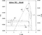
[64]图9是根据本发明的GaAs基PPC50的电流-电压(I-V)特性301和输出功率-电压(P-V)特性401分别与如图1和图2中现有技术条件GaAs基PPC的电流-电压(I-V)特性302和能量转换效率402的比较曲线示意图。所述测量是使用光波长为830nm并且光功率为50mW的光对装置进行照射的条件下完成的。根据本发明GaAs基PPC50获得的最大功率转换率大约为55%,而现有技术能量转换器的功率转换率为45%,而测量时的输出电压Vout大约为6.3伏而相应的输出电流大约为4.5毫安。根据本发明的GaAs基PPC 50所获得的转换率和输出电流,相比现有技术的GaAs基能量转换器大约提高25%,使得根据本发明的PPC的功率转换效率接近理论最大值。所述提高取决于下列因素:(1)p极层的碳掺杂量;这将提高在含有碳掺杂的p型发射极134里的少数载流子的寿命,所述载流子寿命的提高部分原因在于受导电层136和可选光透窗层135的超高掺杂层产生的有利的电场方向影响,以便诱发更强的电场用于新生光生载流子在p-n结里的迁移,以及碳掺杂层具有较低的表面阻抗,所述碳掺杂层包括p型发射层、p型窗层和p型导电层;所述较低的表面阻抗在电流保持很高时仍可提高可实现电压值,较低的表面阻抗和电压的提高都将实现较高的输出功率;(2)装置分块新颖的几何分布形状通过增加中心分块消除位于装置中心的空腔;以及,附加的电流阻挡层131显著降低甚至可能消除任何或所有在邻近分块间的光诱导的电传导,并且所述电传导的降低或消除有助于增加每个分块在光照条件下产生的电压。[64] Fig. 9 is the current-voltage (IV)
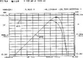
[65]图10是根据本发明的InP基PPC的电流-电压(I-V)特性411和输出功率-电压(P-V)特性410的曲线示意图,所述InP基PPC含有第一多层结构30,所述第一多层结构30含有如上文所述的InGaAs活性层133/134和InP电流阻挡层131。所述装置的最大功率转换效率超过28%,并且测量时输出电压为3.5伏,得到的相应输出电流为8.1毫安。当入射光的波长为1436纳米且功率为100mW时,可获得PPC的最大输出功率大约为28.4mW。对于工作波长范围在1310-1550nm之间的光能量转换器而言,这样高的功率转换效率是显著的改善,其性能参数远超过所有的现有装置。所测量的装置具有9块扇形装置分块。[65] FIG. 10 is a schematic diagram of a current-voltage (I-V)
[66]有利之处在于,根据本发明的InP基PPC的关键目的之一在于可用于光电能量技术,即增加光能量的传输距离,使所述光能量的传输具有足够效率以驱动如传感器和数据接口的远程设备。当距离超过1km时,必须使用范围在1310nm至1550nm之间的长波光,因为利用光纤传输所述范围以外的光时,所述光的衰减相对较高。对于短波光,例如980nm及以下,在常用光纤里传输时的光衰减超过3dB/km,因此,给距离超过几百米的设备供能将被禁止。然而,当波长为1310nm及以上的光在光纤里传输时,其光衰减大约为0.1dB/km或小于0.1dB/km,因此,当光能量需要传送的距离为1km或超过1km时,根据本发明的InP基PPC较GaAs基装置更适于用作能量转换器。另一有利之处在于,根据本发明的PPC可被安装在适合于对准单模光纤的接收元件里,因此,使用根据本发明的InP基PPC可以发挥远程传送光能量的优点。[66] The advantage is that one of the key purposes of the InP-based PPC according to the present invention is that it can be used in photovoltaic energy technology, that is, to increase the transmission distance of light energy, so that the transmission of light energy has sufficient efficiency to drive such as sensors and Data interface to the remote device. When the distance exceeds 1 km, long-wavelength light in the range between 1310 nm and 1550 nm has to be used, since the attenuation of light outside said range is relatively high when optical fiber is used to transmit said light. For short-wavelength light, such as 980nm and below, the optical attenuation exceeds 3dB/km when transmitted in common optical fibers. Therefore, powering devices with a distance of more than a few hundred meters will be prohibited. However, when light with a wavelength of 1310nm and above is transmitted in an optical fiber, its light attenuation is about 0.1dB/km or less than 0.1dB/km. Therefore, when the distance of light energy to be transmitted is 1km or more than 1km, according to this The invented InP-based PPCs are more suitable for use as energy converters than GaAs-based devices. Another advantage is that the PPC according to the present invention can be installed in a receiving element suitable for aligning single-mode optical fibers, so that the use of the InP-based PPC according to the present invention can take advantage of the long-distance transmission of optical energy.
[67]注意,上文描述的根据本发明的光电能量转换器的具体实施例可以利用其他实施例的部分技术特征,并且仅作为示例,在本发明的具体应用中可采用很多元件的可选实施例,这对于本领域技术人员是显而易见的。例如,根据本发明的PPC的其他实施例可以含有装置分块,所述装置分块以圆形组合排列,其中第一组装置分块位于中心并且被第二组装置分块所环绕,所述第二组装置分块包括至少两个装置分块。在这里所述的实施例中,第一组装置分块由单个中心分块55组成,但是在其他实施例中,可以预见,所述装置分块的第一组可以由不止一个装置分块构成,所述第一组装置分块有附加沟槽隔离并且可以串联或彼此绝缘以及逐个寻址。其他实施例可以含有基极层为p-掺杂而发射极为n-掺杂的装置。在其他实施例中,还可以优化PPC中心部分的第二多层结构以产生光,并且可以在第二基极层和发射基层之间不含本征层,或可以使所含有的本征层厚度小于0.1微米,以便形成量子井。[67] Note that the specific embodiment of the photoelectric energy converter described above according to the present invention can utilize some technical features of other embodiments, and it is only used as an example, and many optional components can be used in the specific application of the present invention. Examples are obvious to those skilled in the art. For example, other embodiments of a PPC according to the present invention may contain device tiles arranged in a circular arrangement with a first set of device tiles at the center and surrounded by a second set of device tiles, said The second set of device blocks includes at least two device blocks. In the embodiment described here, the first set of device blocks consists of a single
[68]当然,在不脱离本发明的精神和范围的情况下可以假设大量的其它实施例。[68] Of course, numerous other embodiments can be conceived without departing from the spirit and scope of the invention.
Claims (19)
Translated fromChineseApplications Claiming Priority (3)
| Application Number | Priority Date | Filing Date | Title |
|---|---|---|---|
| US87110806P | 2006-12-20 | 2006-12-20 | |
| US60/871,108 | 2006-12-20 | ||
| US60/871,125 | 2006-12-20 |
Publications (1)
| Publication Number | Publication Date |
|---|---|
| CN101442079Atrue CN101442079A (en) | 2009-05-27 |
Family
ID=40726418
Family Applications (1)
| Application Number | Title | Priority Date | Filing Date |
|---|---|---|---|
| CN 200710301931PendingCN101442079A (en) | 2006-12-20 | 2007-12-20 | Photovoltaic power converter |
Country Status (1)
| Country | Link |
|---|---|
| CN (1) | CN101442079A (en) |
Cited By (1)
| Publication number | Priority date | Publication date | Assignee | Title |
|---|---|---|---|---|
| US11656420B2 (en) | 2021-01-22 | 2023-05-23 | Macleon, LLC | System and method of distributing ultra high power using optical fiber cable |
- 2007
- 2007-12-20CNCN 200710301931patent/CN101442079A/enactivePending
Cited By (4)
| Publication number | Priority date | Publication date | Assignee | Title |
|---|---|---|---|---|
| US11656420B2 (en) | 2021-01-22 | 2023-05-23 | Macleon, LLC | System and method of distributing ultra high power using optical fiber cable |
| US11774695B2 (en) | 2021-01-22 | 2023-10-03 | Macleon, LLC | Optical fiber cable |
| US12117663B2 (en) | 2021-01-22 | 2024-10-15 | Macleon, LLC | System and method of refining optical fiber |
| US12353037B2 (en) | 2021-01-22 | 2025-07-08 | Macleon, LLC | System and method of refining optical fiber |
Similar Documents
| Publication | Publication Date | Title |
|---|---|---|
| US8742251B2 (en) | Multi-segment photovoltaic power converter with a center portion | |
| KR101908742B1 (en) | TYPE-II HIGH BANDGAP TUNNEL JUNCTIONS OF InP LATTICE CONSTANT FOR MULTIJUNCTION SOLAR CELLS | |
| TWI594449B (en) | Four-contact reverse metamorphic multi-contact solar cell with two metamorphic layers | |
| US7119271B2 (en) | Wide-bandgap, lattice-mismatched window layer for a solar conversion device | |
| TWI488316B (en) | Substitute substrate for reverse-junction multi-junction solar cells | |
| US6239354B1 (en) | Electrical isolation of component cells in monolithically interconnected modules | |
| TWI441343B (en) | Heterogeneous junction subcell in reverse metamorphic multi-junction solar cell | |
| JP5502871B2 (en) | Photocell | |
| US20160056317A1 (en) | Low-bandgap, monolithic, multi-bandgap, optoelectronic devices | |
| US20030070707A1 (en) | Wide-bandgap, lattice-mismatched window layer for a solar energy conversion device | |
| JPH05114747A (en) | Improved monolithic tandem-type solar cell | |
| CN101292367A (en) | A photocell comprising two photocells and two photon sources | |
| TW201228004A (en) | Laser energy converting device | |
| US20140090700A1 (en) | High-concentration multi-junction solar cell and method for fabricating same | |
| US20150179857A1 (en) | Semiconductor epitaxial structures and semiconductor optoelectronic devices comprising the same | |
| CN102651420A (en) | Double-junction GaAs lamination laser photovoltaic cell and fabrication method thereof | |
| US11245046B2 (en) | Multi-junction tandem laser photovoltaic cell and manufacturing method thereof | |
| CN101431084A (en) | Multi-segment photovoltaic power converter with a center portion | |
| JP2011077295A (en) | Junction type solar cell | |
| CN220233213U (en) | Heterogeneous semiconductor device, detector and photovoltaic cell | |
| CN101442079A (en) | Photovoltaic power converter | |
| CN112382687B (en) | A planar photoelectric detector and a method for preparing the same | |
| JPH0955522A (en) | Tunnel diode | |
| JPH11274532A (en) | Solar cell | |
| CN106611805A (en) | Photovoltaic device and preparation method thereof, multi-junction GaAs laminated laser photovoltaic cell |
Legal Events
| Date | Code | Title | Description |
|---|---|---|---|
| C06 | Publication | ||
| PB01 | Publication | ||
| C10 | Entry into substantive examination | ||
| SE01 | Entry into force of request for substantive examination | ||
| C02 | Deemed withdrawal of patent application after publication (patent law 2001) | ||
| WD01 | Invention patent application deemed withdrawn after publication | Open date:20090527 |