CN101438408B - Composite LED modules - Google Patents
Composite LED modulesDownload PDFInfo
- Publication number
- CN101438408B CN101438408BCN2005800396012ACN200580039601ACN101438408BCN 101438408 BCN101438408 BCN 101438408BCN 2005800396012 ACN2005800396012 ACN 2005800396012ACN 200580039601 ACN200580039601 ACN 200580039601ACN 101438408 BCN101438408 BCN 101438408B
- Authority
- CN
- China
- Prior art keywords
- light emitting
- emitting diode
- led
- unit
- led unit
- Prior art date
- Legal status (The legal status is an assumption and is not a legal conclusion. Google has not performed a legal analysis and makes no representation as to the accuracy of the status listed.)
- Active
Links
Images


Classifications
- H—ELECTRICITY
- H01—ELECTRIC ELEMENTS
- H01L—SEMICONDUCTOR DEVICES NOT COVERED BY CLASS H10
- H01L25/00—Assemblies consisting of a plurality of semiconductor or other solid state devices
- H01L25/03—Assemblies consisting of a plurality of semiconductor or other solid state devices all the devices being of a type provided for in a single subclass of subclasses H10B, H10D, H10F, H10H, H10K or H10N, e.g. assemblies of rectifier diodes
- H01L25/04—Assemblies consisting of a plurality of semiconductor or other solid state devices all the devices being of a type provided for in a single subclass of subclasses H10B, H10D, H10F, H10H, H10K or H10N, e.g. assemblies of rectifier diodes the devices not having separate containers
- H01L25/075—Assemblies consisting of a plurality of semiconductor or other solid state devices all the devices being of a type provided for in a single subclass of subclasses H10B, H10D, H10F, H10H, H10K or H10N, e.g. assemblies of rectifier diodes the devices not having separate containers the devices being of a type provided for in group H10H20/00
- H01L25/0756—Stacked arrangements of devices
- H—ELECTRICITY
- H01—ELECTRIC ELEMENTS
- H01L—SEMICONDUCTOR DEVICES NOT COVERED BY CLASS H10
- H01L2224/00—Indexing scheme for arrangements for connecting or disconnecting semiconductor or solid-state bodies and methods related thereto as covered by H01L24/00
- H01L2224/01—Means for bonding being attached to, or being formed on, the surface to be connected, e.g. chip-to-package, die-attach, "first-level" interconnects; Manufacturing methods related thereto
- H01L2224/42—Wire connectors; Manufacturing methods related thereto
- H01L2224/47—Structure, shape, material or disposition of the wire connectors after the connecting process
- H01L2224/48—Structure, shape, material or disposition of the wire connectors after the connecting process of an individual wire connector
- H01L2224/4805—Shape
- H01L2224/4809—Loop shape
- H01L2224/48091—Arched
- H—ELECTRICITY
- H01—ELECTRIC ELEMENTS
- H01L—SEMICONDUCTOR DEVICES NOT COVERED BY CLASS H10
- H01L2224/00—Indexing scheme for arrangements for connecting or disconnecting semiconductor or solid-state bodies and methods related thereto as covered by H01L24/00
- H01L2224/73—Means for bonding being of different types provided for in two or more of groups H01L2224/10, H01L2224/18, H01L2224/26, H01L2224/34, H01L2224/42, H01L2224/50, H01L2224/63, H01L2224/71
- H01L2224/732—Location after the connecting process
- H01L2224/73251—Location after the connecting process on different surfaces
- H01L2224/73265—Layer and wire connectors
- H—ELECTRICITY
- H10—SEMICONDUCTOR DEVICES; ELECTRIC SOLID-STATE DEVICES NOT OTHERWISE PROVIDED FOR
- H10H—INORGANIC LIGHT-EMITTING SEMICONDUCTOR DEVICES HAVING POTENTIAL BARRIERS
- H10H20/00—Individual inorganic light-emitting semiconductor devices having potential barriers, e.g. light-emitting diodes [LED]
- H10H20/80—Constructional details
- H10H20/81—Bodies
- H10H20/819—Bodies characterised by their shape, e.g. curved or truncated substrates
- H—ELECTRICITY
- H10—SEMICONDUCTOR DEVICES; ELECTRIC SOLID-STATE DEVICES NOT OTHERWISE PROVIDED FOR
- H10H—INORGANIC LIGHT-EMITTING SEMICONDUCTOR DEVICES HAVING POTENTIAL BARRIERS
- H10H20/00—Individual inorganic light-emitting semiconductor devices having potential barriers, e.g. light-emitting diodes [LED]
- H10H20/80—Constructional details
- H10H20/85—Packages
- H10H20/855—Optical field-shaping means, e.g. lenses
- H10H20/856—Reflecting means
Landscapes
- Engineering & Computer Science (AREA)
- Power Engineering (AREA)
- Microelectronics & Electronic Packaging (AREA)
- Physics & Mathematics (AREA)
- Condensed Matter Physics & Semiconductors (AREA)
- General Physics & Mathematics (AREA)
- Computer Hardware Design (AREA)
- Led Device Packages (AREA)
- Led Devices (AREA)
- Fastening Of Light Sources Or Lamp Holders (AREA)
- Arrangement Of Elements, Cooling, Sealing, Or The Like Of Lighting Devices (AREA)
- Non-Portable Lighting Devices Or Systems Thereof (AREA)
Abstract
Description
Translated fromChinese技术领域technical field
本发明涉及发光二极管(LED)。The present invention relates to light emitting diodes (LEDs).
背景技术Background technique
用于普通照明的LED模块(LED灯,LED发光体等)通常由单个LED制成,或者由二维排列的LED系统制成。LED modules (LED lamps, LED illuminants, etc.) for general lighting are usually made from individual LEDs, or from systems of LEDs arranged two-dimensionally.
LED的特点在于它以良好定义的波长产生单色光的能力。这个特点对很多应用都很有用,但却使白光的产生复杂化,因为根据定义,白光由多个波长的混合而构成。解决此问题的一种方式是向LED添加一种波长转换材料。例如,在蓝光LED上涂上一层能将一些蓝光转换为黄光的波长转换材料。由此,将转换的黄光与未转换的蓝光的混合作为白光来提供。然而,这种白光LED的亮度有限,从而不能满足于那些需要强光输出级的应用。LEDs are characterized by their ability to produce monochromatic light at well-defined wavelengths. This feature is useful for many applications, but complicates the generation of white light, which by definition consists of a mixture of multiple wavelengths. One way to solve this problem is to add a wavelength converting material to the LED. For example, blue LEDs are coated with a wavelength-converting material that converts some of the blue light into yellow light. Thus, a mixture of converted yellow light and unconverted blue light is provided as white light. However, such white LEDs have a limited brightness, which makes them unsuitable for applications that require a strong light output level.
一种替代的解决方式是将来自两个或多个不同颜色LED(即来自于多种LED)的光混合起来。这种多LED的布置还可以简单地通过调整各个LED构件的相对功率,来对颜色外观提供动态调整。An alternative solution is to mix the light from two or more LEDs of different colors (ie from multiple LEDs). This multi-LED arrangement can also provide dynamic adjustments to color appearance simply by adjusting the relative power of the individual LED components.
一种这样的布置披露在JP07015044中,该专利还提出将不同颜色的LED单元放置在不同的高度,以改善光输出。然而,单个LED的亮度却受到限制。对于普通照明目的来说,必需将大量的LED放置在一起,这会使照明设备很笨重。对紧凑应用而言,笨重只是一般问题,然而由于会使同质颜色混合更加复杂,这往往还会带来器件颜色外观的问题。One such arrangement is disclosed in JP07015044, which also proposes placing different colored LED units at different heights to improve light output. However, the brightness of individual LEDs is limited. For general lighting purposes, a large number of LEDs must be placed together, which makes the lighting equipment bulky. Bulkiness is generally an issue for compact applications, however it often presents issues with device color appearance as it complicates homogeneous color mixing.
因此,就需要能够提供高亮度、紧凑以及同质颜色混合的改进的LED。Accordingly, there is a need for improved LEDs that provide high brightness, compactness, and homogenous color mixing.
发明内容Contents of the invention
上述需要借助于权利要求1所述的本发明来满足。本发明其他的优选实施例在附加的从属权利要求中确定。This need is met by means of the invention as claimed in claim 1 . Further preferred embodiments of the invention are defined in the appended dependent claims.
因此,依照本发明的一个方面,提供一种复合多色发光二极管,其包括第一发光二极管单元和第二发光二极管单元。每个发光二极管管单元具有上表面和下表面,并且分别可以工作来穿过其上表面发出第一波长和第二波长的光。另外,第二发光二极管单元的下表面设置在第一发光二极管单元的上表面上。换句话说,第二二极管单元设置在第一二极管单元的顶部,由此占据着第一二极管单元其发光上表面的一部分。因此,两个二极管单元可以设置在一个二极管单元的空间内。这是有利的,因为这可以提供可用空间的最大有效利用以及提供更好的颜色混合。Therefore, according to one aspect of the present invention, there is provided a composite multi-color light emitting diode, which includes a first light emitting diode unit and a second light emitting diode unit. Each LED tube unit has an upper surface and a lower surface, and is operable to emit light of a first wavelength and a second wavelength through the upper surface, respectively. In addition, the lower surface of the second light emitting diode unit is disposed on the upper surface of the first light emitting diode unit. In other words, the second diode unit is arranged on top of the first diode unit, thereby occupying a part of the light-emitting upper surface of the first diode unit. Therefore, two diode units can be arranged in the space of one diode unit. This is advantageous as it can provide the most efficient use of the available space as well as provide better color mixing.
这些发光二极管单元基本上都是传统的LED单元,设置在彼此的顶部上。如现有技术众所周知的那样,LED单元可以具有许多不同的构造。每个LED单元都设置有两个用以提供驱动电压的电极。这些电极可以设置在单元的相对侧上,或者它们可以并排地设置在单元的同一侧上。因此,这些电极可以设置在单元的上侧或下侧。这些电极通常通过互连电路和接线(bond wire)连接在它们的驱动器上。These light emitting diode units are basically conventional LED units arranged on top of each other. As is well known in the art, LED units can have many different configurations. Each LED unit is provided with two electrodes for providing driving voltage. These electrodes may be arranged on opposite sides of the cell, or they may be arranged side by side on the same side of the cell. Therefore, these electrodes can be arranged on the upper side or the lower side of the cell. These electrodes are usually connected to their drivers by interconnecting circuits and bond wires.
然而,依照一个实施例,第一发光二极管单元的上表面和第二发光二极管单元的下表面每个都包括电极,这些电极电互连起来。因此,第一单元和第二单元串联地连接,而不需要使用单独的互联电路或接线。实际上,接线的数目变得有限,从而使得更易于制造,并增大了发光表面(由于否则接线会占据一部分LED光路)。为了提高电和热性能,可以对传统发光二极管的电镀层作出专门的改进。这种附加电镀设计的一部分可以用来将第二二极管单元附接在第一二极管单元上,而另一部分,即电互连的部分可以接收接线,以同时驱动第一二极管的上电极和第二二极管的下电极。However, according to one embodiment, the upper surface of the first light emitting diode unit and the lower surface of the second light emitting diode unit each include electrodes, and the electrodes are electrically interconnected. Therefore, the first unit and the second unit are connected in series without using a separate interconnection circuit or wiring. In fact, the number of wires becomes limited, making it easier to manufacture and increasing the light-emitting surface (since the wires would otherwise occupy part of the LED light path). In order to improve the electrical and thermal performance, special modifications can be made to the plating layer of conventional LEDs. Part of this additional plating design can be used to attach the second diode unit on the first diode unit, while the other part, the part that is electrically interconnected, can receive wiring to simultaneously drive the first diode the upper electrode and the lower electrode of the second diode.
依照本发明,还可以在这种复合LED器件内设置第三LED单元。依照一个实施例,第三LED单元设置在第一发光二极管单元的上表面。由此,两个LED单元并排地设置在第一LED单元上。可替代地,依照另一个实施例,第三LED单元设置在第二发光二极管单元的上表面上。由此提供三个LED单元的堆叠。According to the invention, it is also possible to arrange a third LED unit within such a composite LED device. According to one embodiment, the third LED unit is disposed on the upper surface of the first light emitting diode unit. Thus, two LED units are arranged side by side on the first LED unit. Alternatively, according to another embodiment, the third LED unit is disposed on the upper surface of the second light emitting diode unit. A stack of three LED units is thus provided.
即使LED单元具有相对高的效率,也不可能避免部分驱动电流转换成热而不是光。在高功率LED模块中这特别是成问题的,因为其中热的产生是主要关注的问题。因此,依照一个实施例,LED还包括散热器(heat sink),该散热器设置成接触第一发光二极管单元的下表面,并且可以工作来从所述第一发光二极管单元去除热。该散热器例如可以由具有高导热率和高吸热性的金属制成。Even if an LED unit has a relatively high efficiency, it is impossible to avoid that part of the drive current is converted into heat instead of light. This is particularly problematic in high power LED modules, where heat generation is a major concern. Thus, according to one embodiment, the LED further comprises a heat sink arranged in contact with the lower surface of the first light emitting diode unit and operable to remove heat from said first light emitting diode unit. The heat sink can be made, for example, of a metal with high thermal conductivity and high heat absorption.
根据LED的构造,散热器还可以不仅仅接触第一LED单元。依照一个实施例,散热器还接触第二发光二极管单元的下表面。因此,散热器也可以工作来直接从第二LED单元去除热。Depending on the configuration of the LEDs, the heat sink may also not only be in contact with the first LED unit. According to one embodiment, the heat sink also contacts the lower surface of the second light emitting diode unit. Therefore, the heat sink can also work to remove heat directly from the second LED unit.
传统的LED单元可以理解为由产生光的P/N接口定义的二维结构。基于这种理解,本发明可以解释成三维结构,具有基本上平行排列但以第三维分开的两个或多个二维结构。每个LED单元都提供一个基本垂直于二维结构的光路。本发明的特征还在于设置在第一(底部)LED单元上的LED单元的光路占据了另外由第一LED单元提供的光路的一部分。本发明的一个具体实施例可以解释为包括具有第一发光表面的第一发光二极管,该第一发光二极管承载着具有第二发光表面的第二发光二极管,其中第二发光二极管设置得使从第一表面发出的光完全包围着从第二表面发出的光。从光混合的角度看,这个实施例是特别有利的。A conventional LED unit can be understood as a two-dimensional structure defined by a P/N interface that produces light. Based on this understanding, the present invention can be interpreted as a three-dimensional structure having two or more two-dimensional structures arranged substantially parallel but separated by a third dimension. Each LED unit provides a light path substantially perpendicular to the two-dimensional structure. The invention is also characterized in that the light path of the LED unit arranged on the first (bottom) LED unit occupies a part of the light path otherwise provided by the first LED unit. A particular embodiment of the invention can be interpreted as comprising a first light emitting diode having a first light emitting surface carrying a second light emitting diode having a second light emitting surface, wherein the second light emitting diode is arranged such that The light emitted from one surface completely surrounds the light emitted from the second surface. This embodiment is particularly advantageous from a light mixing point of view.
与传统的LED布置相比,本发明是有利的,因为本发明提供了紧凑而又大功率的、具有高颜色混合度的LED模块。例如,通过组合如蓝光LED单元和黄光LED单元,本发明可以提供紧凑而又高功率的白光LED模块。因此,依照本发明的发光器件可以有利地用作普通照明目的。Compared to conventional LED arrangements, the invention is advantageous because it provides a compact yet powerful LED module with a high degree of color mixing. For example, by combining eg a blue LED unit and a yellow LED unit, the present invention can provide a compact and high power white LED module. Thus, the light emitting device according to the invention can advantageously be used for general lighting purposes.
通常,LED单元的类型有很多。第一类通常相对较薄,在前面的发光表面上带有两个电极极板(electrode pad)。相对的背侧表面通常设计来提供高热导率。在传统的LED布置中,这个背侧表面通常面对着载体基板或者散热器。依照本发明,这个背侧可以可替换地面对着另一LED单元。这些LED单元通常具有比其平面维度至少小两倍的厚度。Generally, there are many types of LED units. The first type is usually relatively thin, with two electrode pads on the front light-emitting surface. The opposing backside surfaces are generally designed to provide high thermal conductivity. In conventional LED arrangements, this backside surface usually faces the carrier substrate or heat sink. According to the invention, this back side can alternatively face another LED unit. These LED units generally have a thickness at least twice smaller than their planar dimensions.
第二类LED单元类似于第一类,但是相反是在背侧设置两个电极极板。从发光角度看这是有利的,因为单元的发光表面不会被接线等阻挡。The second type of LED unit is similar to the first type, but instead has two electrode pads on the backside. This is advantageous from the viewpoint of light emission because the light emitting surface of the unit is not blocked by wiring or the like.
第三类LED单元通常比上述两类稍厚,在每侧带有一个电极极板。换句话说,一个电极极板设置在前面的发光表面上,另一个电极极板设置在相对的背侧表面。The third type of LED unit is usually slightly thicker than the above two types, with an electrode pad on each side. In other words, one electrode pad is provided on the front light-emitting surface and the other electrode pad is provided on the opposite backside surface.
任何一类的LED单元都可以用来构成根据本发明的复合LED模块。薄类型的LED单元优选地被改变来提高电学和热性能。例如,为了有利于进行另一LED单元的传统附接,向顶部表面添加额外的金属电镀。还可以添加电镀结构,以用于附接的LED单元的电互连(类似于接线点(bond wire pad))。Any type of LED unit can be used to form a composite LED module according to the present invention. Thin type LED units are preferably modified to improve electrical and thermal performance. For example, to facilitate conventional attachment of another LED unit, additional metal plating is added to the top surface. Plating structures can also be added for electrical interconnection of attached LED units (similar to bond wire pads).
然而,还可以在顶部表面上使用传统的LED单元而不用任何改变来构成LED堆叠。例如,可以在两个LED单元之间使用中间的传统小片附接材料(die attachmaterial)来附接。However, it is also possible to use conventional LED units on the top surface without any modification to form the LED stack. For example, an intermediate conventional die attach material can be used between the two LED units for attachment.
一旦提供LED堆叠,就可以使用传统的接线工艺来向模块分配剩余的电互连。然而,处理步骤的顺序并不是特定的。例如,可以在附接第二LED单元之前设置第一LED单元的接线。在这种情形中,为了避免在建立下一个互连时之前形成的互连再熔化,可以使用不同类型的焊料,如半导体封装周知的那样。Once the LED stack is provided, conventional wiring techniques can be used to assign the remaining electrical interconnections to the modules. However, the order of processing steps is not specific. For example, the wiring of the first LED unit may be provided before attaching the second LED unit. In this case, in order to avoid remelting of the previously formed interconnect when the next interconnect is made, a different type of solder can be used, as is well known in semiconductor packaging.
一种将LED单元附接在另一LED单元上的传统方式是使用小片附接材料。小片附接材料必须应用在两个LED单元之间,然后执行热处理来建立互连。小片附接材料可以例如是焊料,镀银环氧树脂(silver filled epoxy)或镀银玻璃材料(silver filled glass material)。One conventional way of attaching an LED unit to another LED unit is to use a die attach material. Die attach material must be applied between the two LED units, followed by heat treatment to establish the interconnection. The die attach material can be, for example, solder, silver filled epoxy or silver filled glass material.
实际上,将LED单元附接到另一LED单元上通常会比将LED单元附接在传统的基板上更简单。通常,当将LED单元附接在传统的基板上时,与基板材料相比,LED材料的热膨胀系数(CTE)会存在着实质上的差别。当驱动LED单元时,在LED内会产生热,从而在附接面产生应力负载。当将LED单元附接在LED单元上时,各个材料通常具有更类似的CTE。因此,在LED/LED接口上温度诱导的应力负载会比LED/基板接口上的低。因而,可以使用那些由于CTE不匹配而不适合在传统的互连里使用的很薄、易碎的高导热小片附接材料。In practice, it is often simpler to attach an LED unit to another LED unit than to attach an LED unit to a conventional substrate. Typically, when attaching LED units to conventional substrates, there is a substantial difference in the coefficient of thermal expansion (CTE) of the LED material compared to the substrate material. When the LED unit is driven, heat is generated within the LED, causing stress loads on the attachment surface. The individual materials generally have a more similar CTE when the LED unit is attached to the LED unit. Consequently, temperature-induced stress loads will be lower at the LED/LED interface than at the LED/substrate interface. Thus, thin, brittle, highly thermally conductive die-attach materials that are unsuitable for use in conventional interconnects due to CTE mismatch can be used.
通过以温度控制的方式驱动各个LED单元,可以进一步减小应力负载。例如,第一LED单元的温度可以由其电驱动电流确定,并且通过控制第二LED单元的电驱动电流,第二LED单元的温度可以制成自动地跟随第一LED的温度。The stress load can be further reduced by driving the individual LED units in a temperature controlled manner. For example, the temperature of a first LED unit can be determined by its electrical drive current, and by controlling the electrical drive current of the second LED unit, the temperature of the second LED unit can be made to automatically follow the temperature of the first LED.
附图说明Description of drawings
参看举例说明的附图,将给出优选实施例的详细描述,在附图中:A detailed description of the preferred embodiment will be given with reference to the accompanying drawings which illustrate, in which:
图1说明依照本发明具有彼此堆叠的两个LED单元和三个LED单元的LED模块的顶视图和横截面图;Figure 1 illustrates a top view and a cross-sectional view of an LED module with two LED units and three LED units stacked on top of each other according to the present invention;
图2说明依照本发明具有堆叠在散热器上的三个LED单元的LED模块的横截面图;Figure 2 illustrates a cross-sectional view of an LED module with three LED units stacked on a heat sink in accordance with the present invention;
图3说明排列成一行、形成呼叫灯(line lamp)的光源的八个LED模块;Figure 3 illustrates eight LED modules arranged in a line to form a light source for a line lamp;
图4说明排列成3×3阵列、形成聚光灯的光源的九个LED模块;Figure 4 illustrates nine LED modules arranged in a 3x3 array forming the light source of a spotlight;
图5说明具有用以反射、混合并聚焦从LED发出的光的反射器并具有绝缘封装(dielectric encapsulation)的LED模块;5 illustrates an LED module with a reflector to reflect, mix and focus light emitted from the LED and with dielectric encapsulation;
图6说明类似于图5但还设置有准直器的装置;Figure 6 illustrates a device similar to Figure 5 but also provided with a collimator;
图7说明具有在反射器内排列的LED模块阵列的照明模块的横截面;Figure 7 illustrates a cross-section of a lighting module having an array of LED modules arranged within a reflector;
图8说明复合发光二极管单元的横截面,其中一种小片附接(die-attach)材料被用于附接二极管单元;Figure 8 illustrates a cross-section of a composite light emitting diode unit in which a die-attach material is used to attach the diode unit;
图9是说明从依照本发明的LED模块发出的光的透视图;9 is a perspective view illustrating light emitted from an LED module according to the present invention;
图10说明具有两个并排的堆叠的器件的顶视图和侧视图,每个堆叠都包括三个LED单元;Figure 10 illustrates top and side views of a device with two side-by-side stacks, each stack comprising three LED units;
图11说明使用在第一发光二极管单元上设置的组合电极/焊料垫,堆叠在该第一发光二极管单元顶部的第二发光二极管单元的横截面图;Figure 11 illustrates a cross-sectional view of a second LED unit stacked on top of a first LED unit using a combined electrode/solder pad disposed on the first LED unit;
图12a和12b说明对上面的发光二极管单元提供增强安装的电镀结构的透视图和横截面图。Figures 12a and 12b illustrate perspective and cross-sectional views of a plating structure providing enhanced mounting to an upper LED unit.
具体实施方式Detailed ways
图1说明两种替代的复合LED,LED 100是两种颜色-蓝光100和黄光102复合LED,LED 110是三种颜色-红光103、绿光104以及蓝光105复合LED。Figure 1 illustrates two alternative composite LEDs, LED 100 is a two color - blue 100 and yellow 102 composite LED and LED 110 is a three color - red 103, green 104 and blue 105 composite LED.
在替代的实施例中,如图2所示,复合LED 200设置有散热器204,LED单元201、202以及203排列在散热器204上。散热器204用以在工作期间从LED单元去除热。In an alternative embodiment, as shown in FIG. 2, the
这种复合LED可以有利地用在很多应用中。例如,如图3所示,8×1阵列的复合LED可以设置在呼叫灯300中。在图4中还示出一种采用聚光灯400形式的替代结构,具有3×3阵列的复合LED 401。Such composite LEDs can be used advantageously in many applications. For example, as shown in FIG. 3 , an 8×1 array of composite LEDs may be provided in a
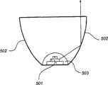
依照一个实施例,如图5所示,复合LED 501可以设置有反射器502。在这样的设置中,复合LED还可以封装在封装材料503中。反射器例如可以由铝形成,并限定一个腔,从复合LED发出的光在该腔内混合并聚焦。依照一种设计,该腔是开放的,由此直接与光模块周围的环境相通。依照另一种设计,如图6所示,腔内填充一种洁净电介质,该电介质形成准直器604,对发出的光具有准直效应。除准直器604之外,图6所示的复合LED类似于图5所示的复合LED,以从6而不是从5开始的相应参考数字指示各个部件。准直器604具有透镜形状,该透镜形状取决于期望的准直效果。特别地,准直器可以具有透镜形状的外表面(如准直器604所指示的),或者可以具有平坦的外表面(未示出)。According to one embodiment, a
反射器通常用来聚焦和混合从复合LED发出的光。依照另一个实施例,多个复合LED 701排列在共同的反射器702内,位于共同的封装层703后面。类似于图6所示的排列,这种复合LED可选地装配有准直器。Reflectors are commonly used to focus and mix the light emitted from composite LEDs. According to another embodiment, multiple
图8是两种颜色的复合LED的横截面图,蓝光LED单元803设置在绿光LED单元802的顶部。该器件设置在散热器801上,中间隔有导热衬垫806。这种下面的绿光LED单元802位于散热器801上的设置类似于传统的单个LED单元。与传统的LED设置一样,接线804附接到LED单元,以提供驱动电压。8 is a cross-sectional view of a composite LED of two colors, with a
上面的蓝光LED单元803借助于传统的小片附接材料805附接在下面的绿光LED单元802上,小片附接材料805用以固定该两个LED单元。上面的LED是直接附接在下面的LED上的。特别地,与LED单元应用在散热器或基板上相比,这种上面的LED单元的应用不必考虑上下LED单元之间热膨胀系数的任何实质差别。基本上,所有的LED单元都具有相同的基本结构,从而在响应温度变化时表现得基本相同。然而,对于例如安装在散热器上的LED单元,情形通常并不如此。The upper
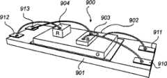
图9说明三色复合LED的示意性透视图,绿光LED 902在底部排列在散热器901上。蓝光LED单元903和红光LED单元904并排地排列在绿光LED单元902上。绿光LED单元和蓝光LED单元都具有它们各自的设置在单元上侧的接触垫,而红光LED单元具有一个设置在上侧的接触垫和一个设置在下侧的接触垫。因此,蓝光LED单元903设置得与绿光LED单元902电分离,而红光LED单元904设置成以其下面的接触垫直接接触绿光LED单元902上面的一个接触垫。由此,只使用两个接线910和912,就可以串联地驱动绿光LED单元和红光LED单元。蓝光LED单元使用接线911和913采用传统的方式驱动。实际上,接线的总数由六个减小到四个,由此降低了制造的复杂性,并提高了器件的有效发光面积。9 illustrates a schematic perspective view of a three-color composite LED, with
图10示出又一个实施例的顶视图和横截面图,蓝光LED单元1003和绿光LED单元1002并排地排列在基板1001上。每个蓝光LED单元和绿光LED单元还具有堆叠在其上的红光LED单元和黄光LED单元1004、1005、1006、1007,由此形成两个并排排列的堆叠,每个堆叠具有彼此堆叠的三个LED单元。依照这个实施例,绿光LED单元和蓝光LED单元每个都具有设置在上侧的接触垫,而红光LED单元和黄光LED单元具有设置在上侧的一个接触垫和设置在下侧的一个接触垫。由此,每个堆叠可以只使用两个接线进行驱动。从光效率方面看,这提供了特别有利的设计。FIG. 10 shows a top view and a cross-sectional view of yet another embodiment, a
图11还示出了另一个实施例,其中绿光LED 1101设置在散热器1105上,并承载着蓝光LED单元1102。绿光LED单元的接触垫都设置在顶侧,而蓝光LED单元的接触垫都设置在下侧,与绿光LED单元的接触垫对准。由此,该两个LED单元可以有效地使用相同的触点,而只需要两个接线1104。FIG. 11 also shows another embodiment, wherein a
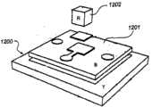
图12说明具有蓝光LED单元1201和红光LED单元1202的复合LED 1200的分解图。12 illustrates an exploded view of a
总之,本发明提供一种复合多色发光二极管器件800,其包括第一发光二极管单元802和设置在该第一发光二极管单元802顶部上的第二发光二极管单元803。因此,本发明提供一种能够发出两种不同的电磁辐射波长的复合发光二极管器件。还可以设置第三发光二极管单元。该第三发光二极管单元可以设置在第二发光二极管单元的顶部,由此提供堆叠的三个发光二极管单元,或者该第三发光二极管单元可以设置在第一发光二极管单元上,由此提供并排地位于第一发光二极管单元顶部上的两个发光二极管单元。In summary, the present invention provides a composite
Claims (7)
Applications Claiming Priority (3)
| Application Number | Priority Date | Filing Date | Title |
|---|---|---|---|
| EP04105910 | 2004-11-19 | ||
| EP04105910.6 | 2004-11-19 | ||
| PCT/IB2005/053756WO2006054236A2 (en) | 2004-11-19 | 2005-11-15 | Composite led modules |
Publications (2)
| Publication Number | Publication Date |
|---|---|
| CN101438408A CN101438408A (en) | 2009-05-20 |
| CN101438408Btrue CN101438408B (en) | 2011-04-20 |
Family
ID=36407519
Family Applications (1)
| Application Number | Title | Priority Date | Filing Date |
|---|---|---|---|
| CN2005800396012AActiveCN101438408B (en) | 2004-11-19 | 2005-11-15 | Composite LED modules |
Country Status (8)
| Country | Link |
|---|---|
| US (1) | US8017955B2 (en) |
| EP (1) | EP1815534B1 (en) |
| JP (1) | JP2008521239A (en) |
| KR (1) | KR101170401B1 (en) |
| CN (1) | CN101438408B (en) |
| AT (1) | ATE519227T1 (en) |
| TW (1) | TW200633265A (en) |
| WO (1) | WO2006054236A2 (en) |
Families Citing this family (40)
| Publication number | Priority date | Publication date | Assignee | Title |
|---|---|---|---|---|
| US9070850B2 (en) | 2007-10-31 | 2015-06-30 | Cree, Inc. | Light emitting diode package and method for fabricating same |
| US9793247B2 (en) | 2005-01-10 | 2017-10-17 | Cree, Inc. | Solid state lighting component |
| US7821023B2 (en) | 2005-01-10 | 2010-10-26 | Cree, Inc. | Solid state lighting component |
| US7829899B2 (en)* | 2006-05-03 | 2010-11-09 | Cree, Inc. | Multi-element LED lamp package |
| DE102006035658B4 (en) | 2006-07-31 | 2013-07-18 | Ivoclar Vivadent Ag | Hand-held light curing device |
| US10295147B2 (en) | 2006-11-09 | 2019-05-21 | Cree, Inc. | LED array and method for fabricating same |
| DE102007011637A1 (en)* | 2007-03-09 | 2008-09-18 | Ivoclar Vivadent Ag | Light emitting device |
| DE102007041896A1 (en)* | 2007-09-04 | 2009-03-05 | Osram Opto Semiconductors Gmbh | Semiconductor device and method for manufacturing a semiconductor device |
| TWI404230B (en)* | 2008-07-15 | 2013-08-01 | Epileds Technologies Inc | Light emitting diodes with multi-layer stacking structure |
| DE102008047579B4 (en) | 2008-09-17 | 2020-02-06 | Osram Opto Semiconductors Gmbh | Lamp |
| US8125344B2 (en)* | 2008-10-13 | 2012-02-28 | Apple Inc. | Portable computer battery indicator |
| US9425172B2 (en) | 2008-10-24 | 2016-08-23 | Cree, Inc. | Light emitter array |
| CN101859757B (en)* | 2009-04-07 | 2014-04-09 | 裕星企业有限公司 | Stack light-emitting diode chip structure and manufacturing method thereof |
| US8486761B2 (en)* | 2010-03-25 | 2013-07-16 | Koninklijke Philips Electronics N.V. | Hybrid combination of substrate and carrier mounted light emitting devices |
| US8319247B2 (en) | 2010-03-25 | 2012-11-27 | Koninklijke Philips Electronics N.V. | Carrier for a light emitting device |
| JP2011249460A (en)* | 2010-05-25 | 2011-12-08 | Meijo University | White light emitting diode |
| US9786811B2 (en) | 2011-02-04 | 2017-10-10 | Cree, Inc. | Tilted emission LED array |
| US8735913B2 (en)* | 2011-04-01 | 2014-05-27 | Visera Technologies Company Limited | Light emitting semiconductor structure |
| US10842016B2 (en) | 2011-07-06 | 2020-11-17 | Cree, Inc. | Compact optically efficient solid state light source with integrated thermal management |
| ES2689918T3 (en) | 2013-05-28 | 2018-11-16 | Sicpa Holding Sa | Sequenced lighting on brand reading devices |
| KR20150019828A (en)* | 2013-08-16 | 2015-02-25 | 삼성전자주식회사 | Light emitting device package and method of manufacturing the same |
| TWI619273B (en)* | 2014-08-08 | 2018-03-21 | High heat dissipation LED package module | |
| KR102358639B1 (en)* | 2016-04-29 | 2022-02-07 | 루미리즈 홀딩 비.브이. | High Brightness Crisp White LED Light Source |
| CN105761633A (en)* | 2016-05-24 | 2016-07-13 | 王德平 | Four-base-color LED display screen and color matching method thereof |
| DE102017102619B4 (en)* | 2017-02-09 | 2022-10-06 | OSRAM Opto Semiconductors Gesellschaft mit beschränkter Haftung | LED unit and LED module |
| KR101931315B1 (en) | 2017-07-21 | 2019-03-13 | 한국광기술원 | Method of manufacturing a display having a hybrid pixel structure |
| US12100696B2 (en) | 2017-11-27 | 2024-09-24 | Seoul Viosys Co., Ltd. | Light emitting diode for display and display apparatus having the same |
| US11282981B2 (en) | 2017-11-27 | 2022-03-22 | Seoul Viosys Co., Ltd. | Passivation covered light emitting unit stack |
| US10892297B2 (en) | 2017-11-27 | 2021-01-12 | Seoul Viosys Co., Ltd. | Light emitting diode (LED) stack for a display |
| US11527519B2 (en) | 2017-11-27 | 2022-12-13 | Seoul Viosys Co., Ltd. | LED unit for display and display apparatus having the same |
| US10892296B2 (en) | 2017-11-27 | 2021-01-12 | Seoul Viosys Co., Ltd. | Light emitting device having commonly connected LED sub-units |
| US10748881B2 (en) | 2017-12-05 | 2020-08-18 | Seoul Viosys Co., Ltd. | Light emitting device with LED stack for display and display apparatus having the same |
| US10886327B2 (en) | 2017-12-14 | 2021-01-05 | Seoul Viosys Co., Ltd. | Light emitting stacked structure and display device having the same |
| US11552057B2 (en) | 2017-12-20 | 2023-01-10 | Seoul Viosys Co., Ltd. | LED unit for display and display apparatus having the same |
| US11522006B2 (en) | 2017-12-21 | 2022-12-06 | Seoul Viosys Co., Ltd. | Light emitting stacked structure and display device having the same |
| US11552061B2 (en) | 2017-12-22 | 2023-01-10 | Seoul Viosys Co., Ltd. | Light emitting device with LED stack for display and display apparatus having the same |
| US11114499B2 (en) | 2018-01-02 | 2021-09-07 | Seoul Viosys Co., Ltd. | Display device having light emitting stacked structure |
| US10784240B2 (en) | 2018-01-03 | 2020-09-22 | Seoul Viosys Co., Ltd. | Light emitting device with LED stack for display and display apparatus having the same |
| US11621253B2 (en)* | 2018-11-02 | 2023-04-04 | Seoul Viosys Co., Ltd. | Light emitting device |
| US11637219B2 (en) | 2019-04-12 | 2023-04-25 | Google Llc | Monolithic integration of different light emitting structures on a same substrate |
Citations (3)
| Publication number | Priority date | Publication date | Assignee | Title |
|---|---|---|---|---|
| US3739241A (en)* | 1971-03-01 | 1973-06-12 | Philips Corp | Electroluminescent semiconductor device containing current controlling rectifying device |
| US6586874B1 (en)* | 1997-05-16 | 2003-07-01 | Kabushiki Kaisha Toshiba | Image display device and light emission device |
| EP1475835A2 (en)* | 2003-04-14 | 2004-11-10 | Epitech Corporation, Ltd. | Color mixing light emitting diode |
Family Cites Families (18)
| Publication number | Priority date | Publication date | Assignee | Title |
|---|---|---|---|---|
| JPS5669880A (en)* | 1979-11-12 | 1981-06-11 | Toshiba Corp | Semiconductor luminous device |
| JPH0715044B2 (en) | 1987-06-19 | 1995-02-22 | 日本エステル株式会社 | Polyester resin composition |
| JPH0691285B2 (en) | 1989-03-10 | 1994-11-14 | 三洋電機株式会社 | Full color light emitting device |
| JP2790237B2 (en) | 1993-06-28 | 1998-08-27 | 日亜化学工業株式会社 | Multicolor light emitting device |
| JPH0846280A (en)* | 1994-07-26 | 1996-02-16 | Mitsubishi Electric Corp | Semiconductor light emitting device |
| US5703436A (en)* | 1994-12-13 | 1997-12-30 | The Trustees Of Princeton University | Transparent contacts for organic devices |
| JP3671457B2 (en)* | 1995-06-07 | 2005-07-13 | 株式会社デンソー | Multilayer board |
| JP2000244020A (en)* | 1999-02-23 | 2000-09-08 | Matsushita Electric Works Ltd | Light source device |
| US6646491B2 (en)* | 2001-05-18 | 2003-11-11 | Eugene Robert Worley, Sr. | LED lamp package for packaging an LED driver with an LED |
| JP3940596B2 (en)* | 2001-05-24 | 2007-07-04 | 松下電器産業株式会社 | Illumination light source |
| JP3940750B2 (en) | 2001-05-24 | 2007-07-04 | 松下電器産業株式会社 | Illumination light source |
| WO2002097884A1 (en)* | 2001-05-26 | 2002-12-05 | Gelcore, Llc | High power led module for spot illumination |
| JP4014377B2 (en) | 2001-09-03 | 2007-11-28 | 豊田合成株式会社 | LED lamp |
| TW522534B (en) | 2001-09-11 | 2003-03-01 | Hsiu-Hen Chang | Light source of full color LED using die bonding and packaging technology |
| US6936856B2 (en) | 2002-01-15 | 2005-08-30 | Osram Opto Semiconductors Gmbh | Multi substrate organic light emitting devices |
| US6960872B2 (en)* | 2003-05-23 | 2005-11-01 | Goldeneye, Inc. | Illumination systems utilizing light emitting diodes and light recycling to enhance output radiance |
| TWM253059U (en)* | 2003-11-05 | 2004-12-11 | Arima Optoelectronics Corp | Full-color light emitting diode formed by overlapping three primary colors |
| EP1641043A1 (en)* | 2004-09-23 | 2006-03-29 | Arima Optoelectronics Corporation | Full-color light-emitting diode (LED) formed by overlaying red, green and blue LED diode dies |
- 2005
- 2005-11-15CNCN2005800396012Apatent/CN101438408B/enactiveActive
- 2005-11-15KRKR1020077013707Apatent/KR101170401B1/enactiveActive
- 2005-11-15ATAT05804145Tpatent/ATE519227T1/ennot_activeIP Right Cessation
- 2005-11-15JPJP2007542402Apatent/JP2008521239A/enactivePending
- 2005-11-15EPEP05804145Apatent/EP1815534B1/enactiveActive
- 2005-11-15WOPCT/IB2005/053756patent/WO2006054236A2/enactiveApplication Filing
- 2005-11-15USUS11/719,300patent/US8017955B2/enactiveActive
- 2005-11-16TWTW094140273Apatent/TW200633265A/enunknown
Patent Citations (3)
| Publication number | Priority date | Publication date | Assignee | Title |
|---|---|---|---|---|
| US3739241A (en)* | 1971-03-01 | 1973-06-12 | Philips Corp | Electroluminescent semiconductor device containing current controlling rectifying device |
| US6586874B1 (en)* | 1997-05-16 | 2003-07-01 | Kabushiki Kaisha Toshiba | Image display device and light emission device |
| EP1475835A2 (en)* | 2003-04-14 | 2004-11-10 | Epitech Corporation, Ltd. | Color mixing light emitting diode |
Also Published As
| Publication number | Publication date |
|---|---|
| US8017955B2 (en) | 2011-09-13 |
| US20090134409A1 (en) | 2009-05-28 |
| EP1815534B1 (en) | 2011-08-03 |
| EP1815534A2 (en) | 2007-08-08 |
| WO2006054236A2 (en) | 2006-05-26 |
| TW200633265A (en) | 2006-09-16 |
| CN101438408A (en) | 2009-05-20 |
| KR101170401B1 (en) | 2012-08-02 |
| JP2008521239A (en) | 2008-06-19 |
| KR20070089172A (en) | 2007-08-30 |
| ATE519227T1 (en) | 2011-08-15 |
| WO2006054236A3 (en) | 2009-07-30 |
Similar Documents
| Publication | Publication Date | Title |
|---|---|---|
| CN101438408B (en) | Composite LED modules | |
| KR102246243B1 (en) | Light emitting element, illumination device and foundation thereof | |
| US9653663B2 (en) | Ceramic LED package | |
| KR102129533B1 (en) | Light emitting element, illumination device and foundation thereof | |
| US7479660B2 (en) | Multichip on-board LED illumination device | |
| US9076940B2 (en) | Solid state lighting component | |
| JP4990355B2 (en) | Semiconductor light emitting device package submount and semiconductor light emitting device package including the submount | |
| US9793247B2 (en) | Solid state lighting component | |
| JP2005158957A (en) | Light emitting device | |
| JP2012532441A (en) | Light emitting diode package | |
| US9929326B2 (en) | LED package having mushroom-shaped lens with volume diffuser | |
| CN110291632B (en) | LED unit | |
| JP3140595U (en) | Light emitting semiconductor device | |
| WO2016184372A2 (en) | Led light source assembly, led photoelectric integration module, and led spotlight | |
| CN201171049Y (en) | Light-emitting semiconductor component |
Legal Events
| Date | Code | Title | Description |
|---|---|---|---|
| C06 | Publication | ||
| PB01 | Publication | ||
| C10 | Entry into substantive examination | ||
| SE01 | Entry into force of request for substantive examination | ||
| C14 | Grant of patent or utility model | ||
| GR01 | Patent grant | ||
| CP01 | Change in the name or title of a patent holder | ||
| CP01 | Change in the name or title of a patent holder | Address after:Eindhoven, Netherlands Patentee after:KONINKLIJKE PHILIPS N.V. Address before:Eindhoven, Netherlands Patentee before:KONINKLIJKE PHILIPS ELECTRONICS N.V. | |
| TR01 | Transfer of patent right | ||
| TR01 | Transfer of patent right | Effective date of registration:20200715 Address after:Holland Schiphol Patentee after:KONINKLIJKE PHILIPS NV Address before:Eindhoven, Netherlands Patentee before:KONINKLIJKE PHILIPS N.V. |