CN101437772B - Thin plate glass laminate, process for producing display device using thin plate glass laminate, and support glass substrate - Google Patents
Thin plate glass laminate, process for producing display device using thin plate glass laminate, and support glass substrateDownload PDFInfo
- Publication number
- CN101437772B CN101437772BCN2007800163971ACN200780016397ACN101437772BCN 101437772 BCN101437772 BCN 101437772BCN 2007800163971 ACN2007800163971 ACN 2007800163971ACN 200780016397 ACN200780016397 ACN 200780016397ACN 101437772 BCN101437772 BCN 101437772B
- Authority
- CN
- China
- Prior art keywords
- glass substrate
- resin layer
- silicone resin
- thin plate
- plate glass
- Prior art date
- Legal status (The legal status is an assumption and is not a legal conclusion. Google has not performed a legal analysis and makes no representation as to the accuracy of the status listed.)
- Expired - Fee Related
Links
Images


Classifications
- B—PERFORMING OPERATIONS; TRANSPORTING
- B32—LAYERED PRODUCTS
- B32B—LAYERED PRODUCTS, i.e. PRODUCTS BUILT-UP OF STRATA OF FLAT OR NON-FLAT, e.g. CELLULAR OR HONEYCOMB, FORM
- B32B17/00—Layered products essentially comprising sheet glass, or glass, slag, or like fibres
- B32B17/06—Layered products essentially comprising sheet glass, or glass, slag, or like fibres comprising glass as the main or only constituent of a layer, next to another layer of a specific material
- B32B17/10—Layered products essentially comprising sheet glass, or glass, slag, or like fibres comprising glass as the main or only constituent of a layer, next to another layer of a specific material of synthetic resin
- B32B17/10005—Layered products essentially comprising sheet glass, or glass, slag, or like fibres comprising glass as the main or only constituent of a layer, next to another layer of a specific material of synthetic resin laminated safety glass or glazing
- B32B17/10009—Layered products essentially comprising sheet glass, or glass, slag, or like fibres comprising glass as the main or only constituent of a layer, next to another layer of a specific material of synthetic resin laminated safety glass or glazing characterized by the number, the constitution or treatment of glass sheets
- B32B17/10036—Layered products essentially comprising sheet glass, or glass, slag, or like fibres comprising glass as the main or only constituent of a layer, next to another layer of a specific material of synthetic resin laminated safety glass or glazing characterized by the number, the constitution or treatment of glass sheets comprising two outer glass sheets
- C—CHEMISTRY; METALLURGY
- C03—GLASS; MINERAL OR SLAG WOOL
- C03C—CHEMICAL COMPOSITION OF GLASSES, GLAZES OR VITREOUS ENAMELS; SURFACE TREATMENT OF GLASS; SURFACE TREATMENT OF FIBRES OR FILAMENTS MADE FROM GLASS, MINERALS OR SLAGS; JOINING GLASS TO GLASS OR OTHER MATERIALS
- C03C27/00—Joining pieces of glass to pieces of other inorganic material; Joining glass to glass other than by fusing
- C03C27/06—Joining glass to glass by processes other than fusing
- C03C27/10—Joining glass to glass by processes other than fusing with the aid of adhesive specially adapted for that purpose
- B—PERFORMING OPERATIONS; TRANSPORTING
- B32—LAYERED PRODUCTS
- B32B—LAYERED PRODUCTS, i.e. PRODUCTS BUILT-UP OF STRATA OF FLAT OR NON-FLAT, e.g. CELLULAR OR HONEYCOMB, FORM
- B32B17/00—Layered products essentially comprising sheet glass, or glass, slag, or like fibres
- B32B17/06—Layered products essentially comprising sheet glass, or glass, slag, or like fibres comprising glass as the main or only constituent of a layer, next to another layer of a specific material
- B32B17/10—Layered products essentially comprising sheet glass, or glass, slag, or like fibres comprising glass as the main or only constituent of a layer, next to another layer of a specific material of synthetic resin
- B32B17/10005—Layered products essentially comprising sheet glass, or glass, slag, or like fibres comprising glass as the main or only constituent of a layer, next to another layer of a specific material of synthetic resin laminated safety glass or glazing
- B32B17/1055—Layered products essentially comprising sheet glass, or glass, slag, or like fibres comprising glass as the main or only constituent of a layer, next to another layer of a specific material of synthetic resin laminated safety glass or glazing characterized by the resin layer, i.e. interlayer
- B—PERFORMING OPERATIONS; TRANSPORTING
- B32—LAYERED PRODUCTS
- B32B—LAYERED PRODUCTS, i.e. PRODUCTS BUILT-UP OF STRATA OF FLAT OR NON-FLAT, e.g. CELLULAR OR HONEYCOMB, FORM
- B32B7/00—Layered products characterised by the relation between layers; Layered products characterised by the relative orientation of features between layers, or by the relative values of a measurable parameter between layers, i.e. products comprising layers having different physical, chemical or physicochemical properties; Layered products characterised by the interconnection of layers
- B32B7/04—Interconnection of layers
- B32B7/06—Interconnection of layers permitting easy separation
- G—PHYSICS
- G02—OPTICS
- G02F—OPTICAL DEVICES OR ARRANGEMENTS FOR THE CONTROL OF LIGHT BY MODIFICATION OF THE OPTICAL PROPERTIES OF THE MEDIA OF THE ELEMENTS INVOLVED THEREIN; NON-LINEAR OPTICS; FREQUENCY-CHANGING OF LIGHT; OPTICAL LOGIC ELEMENTS; OPTICAL ANALOGUE/DIGITAL CONVERTERS
- G02F1/00—Devices or arrangements for the control of the intensity, colour, phase, polarisation or direction of light arriving from an independent light source, e.g. switching, gating or modulating; Non-linear optics
- G02F1/01—Devices or arrangements for the control of the intensity, colour, phase, polarisation or direction of light arriving from an independent light source, e.g. switching, gating or modulating; Non-linear optics for the control of the intensity, phase, polarisation or colour
- G02F1/13—Devices or arrangements for the control of the intensity, colour, phase, polarisation or direction of light arriving from an independent light source, e.g. switching, gating or modulating; Non-linear optics for the control of the intensity, phase, polarisation or colour based on liquid crystals, e.g. single liquid crystal display cells
- G02F1/1303—Apparatus specially adapted to the manufacture of LCDs
- G—PHYSICS
- G02—OPTICS
- G02F—OPTICAL DEVICES OR ARRANGEMENTS FOR THE CONTROL OF LIGHT BY MODIFICATION OF THE OPTICAL PROPERTIES OF THE MEDIA OF THE ELEMENTS INVOLVED THEREIN; NON-LINEAR OPTICS; FREQUENCY-CHANGING OF LIGHT; OPTICAL LOGIC ELEMENTS; OPTICAL ANALOGUE/DIGITAL CONVERTERS
- G02F1/00—Devices or arrangements for the control of the intensity, colour, phase, polarisation or direction of light arriving from an independent light source, e.g. switching, gating or modulating; Non-linear optics
- G02F1/01—Devices or arrangements for the control of the intensity, colour, phase, polarisation or direction of light arriving from an independent light source, e.g. switching, gating or modulating; Non-linear optics for the control of the intensity, phase, polarisation or colour
- G02F1/13—Devices or arrangements for the control of the intensity, colour, phase, polarisation or direction of light arriving from an independent light source, e.g. switching, gating or modulating; Non-linear optics for the control of the intensity, phase, polarisation or colour based on liquid crystals, e.g. single liquid crystal display cells
- G02F1/133—Constructional arrangements; Operation of liquid crystal cells; Circuit arrangements
- G02F1/1333—Constructional arrangements; Manufacturing methods
- G02F1/133302—Rigid substrates, e.g. inorganic substrates
- Y—GENERAL TAGGING OF NEW TECHNOLOGICAL DEVELOPMENTS; GENERAL TAGGING OF CROSS-SECTIONAL TECHNOLOGIES SPANNING OVER SEVERAL SECTIONS OF THE IPC; TECHNICAL SUBJECTS COVERED BY FORMER USPC CROSS-REFERENCE ART COLLECTIONS [XRACs] AND DIGESTS
- Y10—TECHNICAL SUBJECTS COVERED BY FORMER USPC
- Y10T—TECHNICAL SUBJECTS COVERED BY FORMER US CLASSIFICATION
- Y10T428/00—Stock material or miscellaneous articles
- Y10T428/14—Layer or component removable to expose adhesive
- Y10T428/1476—Release layer
- Y—GENERAL TAGGING OF NEW TECHNOLOGICAL DEVELOPMENTS; GENERAL TAGGING OF CROSS-SECTIONAL TECHNOLOGIES SPANNING OVER SEVERAL SECTIONS OF THE IPC; TECHNICAL SUBJECTS COVERED BY FORMER USPC CROSS-REFERENCE ART COLLECTIONS [XRACs] AND DIGESTS
- Y10—TECHNICAL SUBJECTS COVERED BY FORMER USPC
- Y10T—TECHNICAL SUBJECTS COVERED BY FORMER US CLASSIFICATION
- Y10T428/00—Stock material or miscellaneous articles
- Y10T428/24—Structurally defined web or sheet [e.g., overall dimension, etc.]
- Y10T428/24273—Structurally defined web or sheet [e.g., overall dimension, etc.] including aperture
- Y10T428/24322—Composite web or sheet
- Y10T428/24331—Composite web or sheet including nonapertured component
- Y—GENERAL TAGGING OF NEW TECHNOLOGICAL DEVELOPMENTS; GENERAL TAGGING OF CROSS-SECTIONAL TECHNOLOGIES SPANNING OVER SEVERAL SECTIONS OF THE IPC; TECHNICAL SUBJECTS COVERED BY FORMER USPC CROSS-REFERENCE ART COLLECTIONS [XRACs] AND DIGESTS
- Y10—TECHNICAL SUBJECTS COVERED BY FORMER USPC
- Y10T—TECHNICAL SUBJECTS COVERED BY FORMER US CLASSIFICATION
- Y10T428/00—Stock material or miscellaneous articles
- Y10T428/31504—Composite [nonstructural laminate]
- Y10T428/31652—Of asbestos
- Y10T428/31663—As siloxane, silicone or silane
Landscapes
- Chemical & Material Sciences (AREA)
- Engineering & Computer Science (AREA)
- Physics & Mathematics (AREA)
- Nonlinear Science (AREA)
- Chemical Kinetics & Catalysis (AREA)
- General Chemical & Material Sciences (AREA)
- Geochemistry & Mineralogy (AREA)
- Materials Engineering (AREA)
- Organic Chemistry (AREA)
- Life Sciences & Earth Sciences (AREA)
- Ceramic Engineering (AREA)
- Manufacturing & Machinery (AREA)
- Crystallography & Structural Chemistry (AREA)
- General Physics & Mathematics (AREA)
- Optics & Photonics (AREA)
- Laminated Bodies (AREA)
Abstract
Description
Translated fromChinese技术领域technical field
本发明涉及用于液晶显示体、有机EL显示体等显示装置的玻璃基板,更具体地涉及使用薄板玻璃基板来制造显示装置的工序中使用的薄板玻璃基板和支持用玻璃基板的叠层体及使用了该叠层体的显示装置的制造方法,以及薄板玻璃叠层体用的支持用玻璃基板。The present invention relates to glass substrates used in display devices such as liquid crystal displays and organic EL displays, and more particularly to a laminate of a thin glass substrate and a supporting glass substrate used in a process of manufacturing a display device using a thin glass substrate and A method of manufacturing a display device using the laminate, and a supporting glass substrate for a thin glass laminate.
背景技术Background technique
在液晶显示装置(LCD)、有机EL显示装置(OLED)、特别是在移动电话和便携式电话等的便携式显示装置的领域内,显示装置的轻量化、薄型化正成为重要的课题。In the fields of liquid crystal display devices (LCD), organic EL display devices (OLED), and especially portable display devices such as mobile phones and cellular phones, weight reduction and thinning of display devices have become important issues.
为应对该课题,进行了使显示装置所用的玻璃基板的板厚进一步变薄的研究,但如果将玻璃基板的板厚变薄,则强度的下降成为问题,挠曲量也较大,因此无法直接用于目前的制造流水线。In order to cope with this problem, studies have been made to further reduce the thickness of the glass substrate used in the display device. However, if the thickness of the glass substrate is reduced, the decrease in strength becomes a problem, and the amount of warpage is also large, so it cannot be achieved. Directly used in current manufacturing lines.
因此,为了补强板厚较薄的玻璃基板(下面称为“薄板玻璃基板”。)的强度,并确保可用于目前的制造流水线的板厚,提出了如下方法:实施规定的处理,该规定的处理用于在将薄板玻璃基板与其它的支持用玻璃基板贴合形成叠层体(薄板玻璃叠层体)的状态下制造显示装置,上述处理结束后,将薄板玻璃基板和支持用玻璃基板分离,藉此制造显示装置(参照专利文献1~6)。Therefore, in order to reinforce the strength of thin glass substrates (hereinafter referred to as "thin glass substrates"), and to secure thicknesses that can be used in current production lines, a method has been proposed: performing prescribed processes, which stipulate The processing is used to manufacture a display device in a state where a thin glass substrate and another supporting glass substrate are bonded together to form a laminate (thin glass laminate). After the above-mentioned processing is completed, the thin glass substrate and the supporting glass substrate By separating, a display device is produced (see
这些制造显示装置的方法中,作为使薄板玻璃基板和支持用玻璃基板层叠并固定的方法,提出了利用玻璃基板间产生的静电吸附力或真空吸附力将两者固定的方法(例如参照专利文献1),利用玻璃料将玻璃基板的两端固定的方法(例如参照专利文献2),对周缘部的端面附近照射激光、使2块玻璃基板融合的方法(例如参照专利文献3),或在玻璃基板间以覆盖整个表面的状态配置再剥离性的粘着剂或粘着片、利用其粘着力将两者固定的方法(例如参照专利文献4~6)等。In these methods of manufacturing a display device, as a method of laminating and fixing a thin glass substrate and a supporting glass substrate, a method of fixing them by using an electrostatic attraction force or a vacuum attraction force generated between the glass substrates has been proposed (for example, refer to Patent Document 1) A method of fixing both ends of a glass substrate with glass frit (for example, refer to Patent Document 2), a method of irradiating laser light near the end surface of the peripheral portion to fuse two glass substrates (for example, refer to Patent Document 3), or A method in which a releasable adhesive or an adhesive sheet is placed between the glass substrates in a state covering the entire surface, and the adhesive force thereof is used to fix both (for example, refer to Patent Documents 4 to 6) and the like.
这些方法具有可能会对所制造的显示装置造成恶劣影响的潜在的问题点。These methods have potential problems that may adversely affect the manufactured display device.
即,利用玻璃基板间产生的静电吸附力或真空吸附力进行固定的方法,利用玻璃料将玻璃基板的两端固定的方法,或对周缘部的端面附近照射激光、使2块玻璃基板融合的方法中,在不间隔任何的中间层使玻璃基板层叠密合的过程中,难以避免气泡的混入和夹杂了尘垢等异物而产生的凸状缺陷,很难得到表面平滑的玻璃基板叠层体。That is, a method of fixing by electrostatic attraction force or vacuum adsorption force generated between the glass substrates, a method of fixing both ends of the glass substrates with glass frit, or a method of fusing two glass substrates by irradiating laser light near the end faces of the peripheral parts. In the method, in the process of laminating and bonding the glass substrates without any interlayer, it is difficult to avoid the entrainment of air bubbles and convex defects caused by inclusion of foreign matter such as dirt, and it is difficult to obtain a glass substrate laminate with a smooth surface.
采用在玻璃基板间以覆盖整个表面的状态配置再剥离性的粘着剂或粘着片的方法时,可认为与将玻璃基板直接层叠的情况相比,容易避免气泡的混入,且由异物导致的凸状缺陷的产生也较少。然而,薄板玻璃基板和支持用玻璃基板的分离变得困难,分离时薄板玻璃基板可能会破损。例如,可以向薄板玻璃基板和支持用玻璃基板之间插入剃刀的刀刃,藉此作为分离的切入点,但此时,剃刀的刀刃可能会损伤玻璃基板。此外,将两玻璃基板分离时,板厚较薄的薄板玻璃基板可能会碎裂。此外,也有分离后的薄板玻璃基板上残存粘着剂的问题。另外,如同绝缘膜和取向膜的烧成工序,显示装置的制造工序中包含需要高温处理的工序,因此粘着剂及粘着片被要求作为显示装置用材料时的耐热性,但是,未提出耐热性和再剥离性并存的方法。When the method of arranging a re-peelable adhesive or an adhesive sheet between the glass substrates in a state covering the entire surface, it is considered that it is easier to avoid the mixing of air bubbles than the case of directly laminating the glass substrates, and it is considered that the convexity caused by foreign matter The occurrence of shape defects is also less. However, separation of the thin glass substrate and the supporting glass substrate becomes difficult, and the thin glass substrate may be damaged during separation. For example, a razor blade may be inserted between the thin glass substrate and the support glass substrate as an entry point for separation, but in this case, the glass substrate may be damaged by the razor blade. In addition, when the two glass substrates are separated, the thinner glass substrate may be broken. In addition, there is also a problem that the adhesive remains on the separated thin glass substrate. In addition, like the firing process of the insulating film and the alignment film, the manufacturing process of the display device includes a process that requires high-temperature treatment, so the heat resistance of the adhesive and the adhesive sheet is required as a material for the display device. A method that combines heat and re-peelability.
专利文献1:日本专利特开2000—241804号公报Patent Document 1: Japanese Patent Laid-Open No. 2000-241804
专利文献2:日本专利特开昭58—54316号公报Patent Document 2: Japanese Patent Laid-Open No. 58-54316
专利文献3:日本专利特开2003—216068号公报Patent Document 3: Japanese Patent Laid-Open No. 2003-216068
专利文献4:日本专利特开平8—86993号公报Patent Document 4: Japanese Patent Laid-Open No. 8-86993
专利文献5:日本专利特开平9—105896号公报Patent Document 5: Japanese Patent Laid-Open No. 9-105896
专利文献6:日本专利特开2000—252342号公报Patent Document 6: Japanese Patent Laid-Open No. 2000-252342
发明的揭示disclosure of invention
为解决上述现有技术的问题点,本发明的目的是提供抑制薄板玻璃基板和支持用玻璃基板的气泡的混入和异物导致的凸状缺陷的产生、薄板玻璃基板和支持用玻璃基板的分离容易、且耐热性优异的薄板玻璃叠层体,及使用了该薄板玻璃叠层体的显示装置的制造方法,以及该薄板玻璃叠层体用的支持用玻璃基板。In order to solve the above-mentioned problems of the prior art, an object of the present invention is to provide a device that can easily separate the thin glass substrate and the supporting glass substrate by suppressing the mixing of air bubbles between the thin glass substrate and the supporting glass substrate and the generation of convex defects caused by foreign matter. , and a thin glass laminate excellent in heat resistance, a method for manufacturing a display device using the thin glass laminate, and a supporting glass substrate for the thin glass laminate.
为达成上述目的,本发明提供一种薄板玻璃叠层体,它是使薄板玻璃基板和支持用玻璃基板层叠而成的薄板玻璃叠层体,其特征在于,上述薄板玻璃基板和上述支持用玻璃基板隔着具有易剥离性及非粘着性的硅氧烷树脂层(silicone resin layer)层叠,且上述硅氧烷树脂层和上述支持用玻璃基板上设置有至少1个相互连通的孔(下面称为本发明的薄板玻璃叠层体。)。To achieve the above object, the present invention provides a thin glass laminate, which is a thin glass laminate obtained by laminating a thin glass substrate and a supporting glass substrate, wherein the thin glass substrate and the supporting glass The substrates are laminated with an easily peelable and non-adhesive silicone resin layer (silicone resin layer), and the above-mentioned silicone resin layer and the above-mentioned supporting glass substrate are provided with at least one interconnected hole (hereinafter referred to as It is the sheet glass laminate of the present invention.).
本发明的薄板玻璃叠层体中,上述支持用玻璃基板的孔的直径较好为0.1mm~10mm。In the thin-plate glass laminate of the present invention, the diameter of the holes in the supporting glass substrate is preferably from 0.1 mm to 10 mm.
本发明的薄板玻璃叠层体中,上述硅氧烷树脂层较好的是还具有低硅氧烷(silicone)转移性。In the thin-plate glass laminate of the present invention, it is preferable that the silicone resin layer further has low silicone migration properties.
本发明的薄板玻璃叠层体中,上述硅氧烷树脂层较好的是由剥离纸用硅氧烷的固化物构成的层。In the thin-plate glass laminate of the present invention, the silicone resin layer is preferably a layer composed of a cured product of silicone for release paper.
本发明的薄板玻璃叠层体中,上述剥离纸用硅氧烷的固化物较好的是两末端、或两末端及侧链中具有乙烯基的直链状聚有机硅氧烷与甲基氢聚硅氧烷(methyl hydrogen polysiloxane)的交联反应物。In the thin plate glass laminate of the present invention, the cured product of the silicone for release paper is preferably a linear polyorganosiloxane having vinyl groups at both terminals, or both terminals and side chains, and methyl hydrogen. Cross-linking reactant of polysiloxane (methyl hydrogen polysiloxane).
本发明的薄板玻璃叠层体中,较好的是上述薄板玻璃基板的厚度不足0.3mm,上述支持用玻璃基板和上述硅氧烷树脂层的厚度的总和为0.5mm以上。In the thin glass laminate of the present invention, it is preferable that the thickness of the thin glass substrate is less than 0.3 mm, and the total thickness of the supporting glass substrate and the silicone resin layer is 0.5 mm or more.
本发明的薄板玻璃叠层体中,较好的是上述支持用玻璃基板的线膨胀系数和上述薄板玻璃基板的线膨胀系数的差为15×10-7/℃以下。In the thin-plate glass laminate of the present invention, it is preferable that the difference between the linear expansion coefficient of the support glass substrate and the linear expansion coefficient of the thin-plate glass substrate is 15×10-7 /°C or less.
此外,本发明提供一种使用了薄板玻璃叠层体的显示装置的制造方法,它是使用薄板玻璃基板的显示装置的制造方法,其特征在于,具有:Furthermore, the present invention provides a method of manufacturing a display device using a thin glass laminate, which is a method of manufacturing a display device using a thin glass substrate, characterized in that it has:
在具备至少1个孔的支持用玻璃基板上形成硅氧烷树脂层的工序,该硅氧烷树脂层具有易剥离性及非粘着性,且具有至少1个与上述支持用玻璃基板所具备的孔连通的孔,A step of forming a silicone resin layer on a support glass substrate having at least one hole, the silicone resin layer has easy peelability and non-adhesiveness, and has at least one of the above-mentioned support glass substrates. connected holes,
在上述支持用玻璃基板的上述硅氧烷树脂层形成面上层叠薄板玻璃基板的工序,A step of laminating a thin glass substrate on the surface of the above-mentioned support glass substrate on which the silicone resin layer is formed,
为了在上述薄板玻璃基板上制造显示装置而实施处理的工序,和A process of performing a treatment for manufacturing a display device on the above-mentioned thin glass substrate, and
从上述支持用玻璃基板所具备的孔向上述硅氧烷树脂层和上述薄板玻璃基板的界面注入压缩气体,将上述薄板玻璃基板和上述支持用玻璃基板分离的工序。A step of injecting compressed gas into the interface between the silicone resin layer and the thin glass substrate through holes provided in the supporting glass substrate to separate the thin glass substrate and the supporting glass substrate.
本发明的显示装置的制造方法中,上述硅氧烷树脂层较好的是由剥离纸用硅氧烷的固化物构成的层。In the method for producing a display device according to the present invention, the silicone resin layer is preferably a layer composed of a cured product of silicone for release paper.
本发明的显示装置的制造方法中,上述剥离纸用硅氧烷的固化物较好的是两末端、或两末端及侧链中具有乙烯基的直链状聚有机硅氧烷与甲基氢聚硅氧烷的交联反应物。In the method for producing a display device according to the present invention, the cured product of the silicone for release paper is preferably a straight-chain polyorganosiloxane having a vinyl group at both ends, or both ends and side chains, and methyl hydrogen. Cross-linking reactant of polysiloxane.
本发明的显示装置的制造方法中,在支持用玻璃基板上形成上述硅氧烷树脂层的工序较好的是通过在上述支持用玻璃基板上涂布剥离纸用硅氧烷,之后使上述剥离纸用硅氧烷固化来进行。In the manufacturing method of the display device of the present invention, the step of forming the above-mentioned silicone resin layer on the glass substrate for support is preferably by coating silicone for release paper on the above-mentioned glass substrate for support, and then making the above-mentioned release paper The paper is cured with silicone.
本发明的显示装置的制造方法中,上述剥离纸用硅氧烷较好的是含有两末端、或两末端及侧链中具有乙烯基的直链状聚有机硅氧烷,甲基氢聚硅氧烷及铂系催化剂。In the method for producing a display device according to the present invention, the above-mentioned silicone for release paper preferably contains linear polyorganosiloxane having vinyl groups at both terminals, or both terminals and side chains, methyl hydrogen polysiloxane Oxane and platinum catalysts.
本发明的显示装置的制造方法中,上述剥离纸用硅氧烷较好的是不含非反应性硅氧烷。In the manufacturing method of the display device of this invention, it is preferable that the said silicone for release paper does not contain a non-reactive silicone.
本发明的显示装置的制造方法中,上述剥离纸用硅氧烷的涂布较好的是使用网版印刷法。In the manufacturing method of the display device of the present invention, it is preferable to use a screen printing method for coating the silicone for release paper.
本发明的显示装置的制造方法中,较好的是涂布上述剥离纸用硅氧烷后,使其在50~250℃的温度下加热固化。In the manufacturing method of the display device of this invention, it is preferable to heat-cure at the temperature of 50-250 degreeC after apply|coating the said silicone for release papers.
本发明的显示装置的制造方法中,在上述支持用玻璃基板的上述硅氧烷树脂层形成面上层叠薄板玻璃基板的工序较好的是使用真空加压或真空层压。In the method for manufacturing a display device of the present invention, it is preferable to use vacuum pressurization or vacuum lamination in the step of laminating the thin glass substrate on the siloxane resin layer-forming surface of the support glass substrate.
此外,本发明提供一种支持用玻璃基板,它是用于与薄板玻璃基板层叠的支持用玻璃基板,其特征在于,在上述支持用玻璃基板的一个面上形成有具有易剥离性及非粘着性的硅氧烷树脂层,上述支持用玻璃基板和上述硅氧烷树脂层上设置有至少1个相互连通的孔。In addition, the present invention provides a glass substrate for support, which is a glass substrate for support used for lamination with a thin glass substrate, characterized in that, on one surface of the above-mentioned glass substrate for support is formed a A permanent silicone resin layer, at least one hole communicating with each other is provided on the above-mentioned support glass substrate and the above-mentioned silicone resin layer.
本发明的薄板玻璃叠层体是薄板玻璃基板和支持用玻璃基板隔着具有柔软性的硅氧烷树脂层层叠而成的,因此具有层叠时难以混入气泡、而且在混入气泡时也可通过使用轧辊或压机等进行压接来容易地除去该气泡的优点。特别是在使用真空层压法或真空加压法实施薄板玻璃基板和支持用玻璃基板的层叠时,气泡的混入被抑制,密合性也良好。此外,使用真空层压法或真空加压法实施薄板玻璃基板和支持用玻璃基板的层叠时,也具有即使在残存有少量的气泡的情况下、气泡也不会因加热而成长、难以引起薄板玻璃基板的凸状缺陷的优点。The thin glass laminate of the present invention is formed by laminating a thin glass substrate and a support glass substrate through a flexible silicone resin layer, so it is difficult to get air bubbles during lamination, and can also be used when air bubbles are mixed. There is an advantage that the air bubbles can be easily removed by crimping with a roll or a press. In particular, when the thin glass substrate and the supporting glass substrate are laminated using a vacuum lamination method or a vacuum press method, the incorporation of air bubbles is suppressed and the adhesion is also good. In addition, when a thin glass substrate and a support glass substrate are laminated using a vacuum lamination method or a vacuum press method, even if a small amount of air bubbles remain, the air bubbles do not grow due to heating, and it is difficult to cause a thin plate. Advantages of convex defects in glass substrates.
此外,也具有即使在尘垢等异物混入层叠界面时、也可通过具有柔软性的硅氧烷树脂层的形变使其难以引起薄板玻璃叠层体的凸状缺陷的优点。In addition, even when foreign matters such as dirt are mixed into the lamination interface, the deformation of the flexible silicone resin layer makes it difficult to cause convex defects in the thin-plate glass laminate.
此外,介于薄板玻璃基板和支持用玻璃基板之间的层是耐热性优异的硅氧烷树脂层,因此耐热性也良好。In addition, since the layer interposed between the thin glass substrate and the supporting glass substrate is a silicone resin layer excellent in heat resistance, the heat resistance is also good.
本发明的薄板玻璃叠层体是薄板玻璃基板和支持用玻璃基板隔着具有易剥离性及非粘着性的硅氧烷树脂层层叠而成的,因此可容易地将薄板玻璃基板和支持用玻璃基板分离,分离玻璃基板时,薄板玻璃基板不会破损。另外,将薄板玻璃叠层体在大气中以300℃的温度加热1小时后,也同样可以发挥该特性。因此,适合在伴随着加热处理的显示装置的制造工序中使用。The thin glass laminate of the present invention is formed by laminating a thin glass substrate and a supporting glass substrate through an easily peelable and non-adhesive silicone resin layer, so that the thin glass substrate and the supporting glass can be easily bonded together. When the substrate is separated and the glass substrate is separated, the thin glass substrate will not be damaged. In addition, this characteristic can also be exhibited similarly after heating the thin plate glass laminate at a temperature of 300° C. for 1 hour in the air. Therefore, it is suitable for use in a manufacturing process of a display device accompanied by heat treatment.
本发明的薄板玻璃叠层体从设置于支持用玻璃基板上的孔向薄板玻璃基板和硅氧烷树脂层的界面注入压缩气体,藉此可在不施加会引起薄板玻璃的玻璃破损的应力的情况下,将薄板玻璃基板和支持用玻璃基板分离。In the thin glass laminate of the present invention, compressed gas can be injected into the interface between the thin glass substrate and the silicone resin layer from the hole provided in the supporting glass substrate, thereby making it possible to apply stress that would cause glass breakage of the thin glass without applying stress. In this case, the thin glass substrate and the supporting glass substrate are separated.
此外,如果硅氧烷树脂层具有低硅氧烷转移性,则分离玻璃基板时,硅氧烷树脂层中的成分难以向薄板玻璃基板转移。因此,分离后,形成有硅氧烷树脂层的支持用玻璃基板可在与其它薄板玻璃基板的层叠中反复使用。此外,因为硅氧烷树脂层中的成分难以转移至分离后的薄板玻璃基板的表面,所以在薄板玻璃基板的表面贴附偏光板等时不会发生贴附不良等。In addition, when the silicone resin layer has low siloxane transferability, components in the silicone resin layer are less likely to transfer to the thin glass substrate when the glass substrate is separated. Therefore, after separation, the support glass substrate on which the silicone resin layer was formed can be repeatedly used for lamination with other thin glass substrates. In addition, since components in the silicone resin layer are less likely to migrate to the surface of the separated thin glass substrate, adhesion failure or the like does not occur when a polarizing plate or the like is attached to the surface of the thin glass substrate.
本发明的显示装置的制造方法通过使用本发明的薄板玻璃叠层体,可防止薄板玻璃基板的挠曲的发生和制造时的薄板玻璃基板的破损,并且可防止薄板玻璃基板和支持用玻璃基板分离时的薄板玻璃基板的破损,所以可提高所制造的显示装置的原材料利用率。In the method for manufacturing a display device of the present invention, by using the thin glass laminate of the present invention, occurrence of warping of the thin glass substrate and breakage of the thin glass substrate during manufacture can be prevented, and the thin glass substrate and the supporting glass substrate can be prevented from being damaged. The breakage of the thin glass substrate during separation can improve the raw material utilization rate of the manufactured display device.
本发明的显示装置的制造方法中,使用真空加压或真空层压来实施在支持用玻璃基板的硅氧烷树脂层形成面上层叠薄板玻璃基板的工序时,可抑制该硅氧烷树脂层中的气泡的混入。结果,可抑制在真空下形成ITO等透明电极的工序中由混入硅氧烷树脂层的气泡引起的缺陷的产生。In the manufacturing method of the display device of the present invention, when the step of laminating the thin glass substrate on the siloxane resin layer-forming surface of the supporting glass substrate is carried out using vacuum pressurization or vacuum lamination, the siloxane resin layer can be suppressed. Incorporation of air bubbles. As a result, it is possible to suppress the occurrence of defects caused by air bubbles mixed into the silicone resin layer in the step of forming a transparent electrode such as ITO under vacuum.
对附图的简单说明A brief description of the attached drawings
图1是表示本发明的薄板玻璃叠层体的一例的截面模式图。Fig. 1 is a schematic cross-sectional view showing an example of a thin-plate glass laminate of the present invention.
图2是从下方观察图1所示的薄板玻璃叠层体的平面图。Fig. 2 is a plan view of the sheet glass laminate shown in Fig. 1 viewed from below.
图3是表示本发明所用的支持用玻璃基板的变形例的平面图。Fig. 3 is a plan view showing a modified example of the supporting glass substrate used in the present invention.
图4是表示将图1所示的薄板玻璃叠层体的薄板玻璃基板和支持用玻璃基板分离的步骤的图。Fig. 4 is a diagram showing a step of separating a thin glass substrate and a supporting glass substrate of the thin glass laminate shown in Fig. 1 .
图5(a)、(b)是表示实施液晶阵列·滤色片贴合工序后的显示装置中,将薄板玻璃基板和支持用玻璃基板分离的步骤的图。5( a ) and ( b ) are diagrams showing steps of separating a thin glass substrate and a supporting glass substrate in a display device after a liquid crystal array and color filter lamination step.
图6是表示实施例1中,将薄板玻璃叠层体1的薄板玻璃基板和支持用玻璃基板分离的步骤的图。FIG. 6 is a diagram showing a step of separating the thin glass substrate and the supporting glass substrate of the
图7是表示实施例1~3的剥离试验的结果的图。FIG. 7 is a graph showing the results of peeling tests in Examples 1 to 3. FIG.
图8实施例4中使用的支持用玻璃基板的平面图。FIG. 8 is a plan view of a supporting glass substrate used in Example 4. FIG.
符号说明Symbol Description
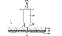
1:薄板玻璃叠层体1: Sheet glass laminate
11:薄板玻璃基板11: Thin glass substrate
12:支持用玻璃基板12: Support glass substrate
13:硅氧烷树脂层13: Silicone resin layer
14:孔14: hole
20:显示装置20: Display device
21:封接材料21: Sealing material
22:结构物22: Structures
30:压缩气体(压缩空气)注入用的管子30: Tube for compressed gas (compressed air) injection
40:密封材料40: sealing material
50:固定台50: fixed table
实施发明的最佳方式The best way to practice the invention
下面,参照附图对本发明的薄板玻璃叠层体进行说明。图1是表示本发明的薄板玻璃叠层体的一例的截面模式图。图2是从下方观察图1所示的薄板玻璃叠层体的平面图。Next, the thin-plate glass laminate of the present invention will be described with reference to the drawings. Fig. 1 is a schematic cross-sectional view showing an example of a thin-plate glass laminate of the present invention. Fig. 2 is a plan view of the sheet glass laminate shown in Fig. 1 viewed from below.
如图1所示,本发明的薄板玻璃叠层体1中,薄板玻璃基板11和支持用玻璃基板12隔着具有易剥离性及非粘着性的硅氧烷树脂层(下面,本说明书中也有称为“硅氧烷树脂层”的情况。)13层叠。支持用玻璃基板12和硅氧烷树脂层13上设置有相互连通的孔14。下面,本说明书中,无特别叙述时,将呈相互连通的关系的设置于支持用玻璃基板12上的孔、及形成于硅氧烷树脂层13上的孔一并记作孔14。如图2所示,孔14形成于支持用玻璃基板12的中心部。As shown in FIG. 1, in the thin-
详细情况如后所述,但本发明的薄板玻璃叠层体1中,可通过孔14将压缩气体注入硅氧烷树脂层13和薄板玻璃基板11的界面,藉此容易地将薄板玻璃基板11和支持用玻璃基板12分离。Details will be described later, but in the thin-
下面,就本发明的薄板玻璃叠层体1的各个结构要素进行说明。Next, each constituent element of the
薄板玻璃基板11是LCD、OLED的显示装置用的玻璃基板,具有不足0.3mm的厚度。薄板玻璃基板11的厚度较好为0.2mm以下,更好为0.1mm以下。此外,薄板玻璃基板11的厚度较好为0.05mm以上。The
另外,作为本发明的对象的显示装置主要是便携式电话和PDA之类的移动终端中使用的小型的显示装置。显示装置主要是LCD或OLED,作为LCD,包括TN型、STN型、FE型、TFT型、MIM型。In addition, the display devices targeted by the present invention are mainly small display devices used in mobile terminals such as mobile phones and PDAs. Display devices are mainly LCDs or OLEDs, and LCDs include TN type, STN type, FE type, TFT type, and MIM type.
热收缩率、表面形状、耐化学品性等薄板玻璃基板11所要求的特性根据显示装置的种类的不同而不同。因此,薄板玻璃基板可以是碱玻璃制的玻璃基板。但是,因为热收缩率较小,所以较好的是无碱玻璃。Properties required for the
本发明中,薄板玻璃基板11较好的是热收缩率较小的玻璃基板。对于玻璃,使用JIS R3102(1995年)规定的线膨胀系数作为热膨胀及热收缩的指标。薄板玻璃基板11的线膨胀系数较好为50×10-7/℃以下,更好为45×10-7/℃以下,进一步更好为40×10-7/℃以下,再进一步好为30×10-7/℃以下,特好为20×10-7/℃以下。In the present invention, the
支持用玻璃基板12是以补强薄板玻璃基板11的强度为目的而与薄板玻璃基板11层叠的支持用玻璃基板,因此必须比薄板玻璃基板11厚。支持用玻璃基板12的厚度较好的是可使其与薄板玻璃基板11的叠层体在目前的制造流水线上流动的厚度。例如,目前的制造流水线是设计为使厚度为0.5mm的基板流动的流水线,薄板玻璃基板11的厚度为0.1mm时,支持用玻璃基板12的厚度较好的是与硅氧烷树脂层13的厚度相加为0.4mm。The supporting
另外,如上所述,薄板玻璃基板11的厚度较好为0.2mm以下。目前的制造流水线中最常见的是设计为使厚度为0.7mm的玻璃基板流动的流水线。因此,支持用玻璃基板12和硅氧烷树脂层13的总计厚度较好为0.5mm以上。但是,制造流水线不限定于设计为使厚度为0.5mm或0.7mm的玻璃基板流动的流水线,也有设计为使除此以外的厚度的玻璃基板流动的情况。例如,有设计为使厚度不足0.5mm的玻璃基板流动的情况,也有设计为使厚度超过0.7mm的玻璃基板流动的情况。In addition, as described above, the thickness of the
如果考虑后述的硅氧烷树脂层13的厚度,则支持用玻璃基板12的厚度较好为0.3~0.8mm。此外,支持用玻璃基板12和硅氧烷树脂层13的厚度的总和较好为0.5mm以上、1.0mm以下。In consideration of the thickness of the
此外,因为支持用玻璃基板12是补强薄板玻璃基板11的强度的支持用玻璃基板,所以其材质无特别限制,可以是碱玻璃或无碱玻璃中的任一种。但是,支持用玻璃基板12较好的是其线膨胀系数与薄板玻璃基板11的线膨胀系数没有很大不同。这是因为,支持用玻璃基板12的线膨胀系数大于薄板玻璃基板11的线膨胀系数时,显示装置的制造工序中的加热工序中,支持用玻璃基板12的膨胀被薄板玻璃叠层体1抑制,因此薄板玻璃叠层体1产生翘曲;相反地,支持用玻璃基板12的线膨胀系数小于薄板玻璃基板11的线膨胀系数时,会发生由薄板玻璃基板11的膨胀导致薄板玻璃基板11从硅氧烷树脂层13剥离的不良情况。In addition, since the supporting
如上所述,支持用玻璃基板12和薄板玻璃基板11的线膨胀系数只要没有很大不同即可,因此不要求两者的线膨胀系数完全一致,可以稍有差别。薄板玻璃基板11和支持用玻璃基板12的线膨胀系数的差较好为35×10-7/℃以下,更好为25×10-7/℃以下,进一步更好为15×10-7/℃以下。As described above, the linear expansion coefficients of the supporting
另外,支持用玻璃基板12在补强薄板玻璃基板11的同时,也在薄板玻璃叠层体1于制造流水线上移动时成为支承薄板玻璃基板11的基台,因此,其尺寸较好的是与薄板玻璃基板11的尺寸相等,或大于薄板玻璃基板11的尺寸。In addition, the supporting
支持用玻璃基板12及硅氧烷树脂层13上设置有至少1个相互连通的孔14。即,支持用玻璃基板12及硅氧烷树脂层13上,在薄板玻璃叠层体1的状态(使支持用玻璃基板12和硅氧烷树脂层13叠层的状态)下相互一致的位置上分别设置有至少1个的孔14。At least one
将薄板玻璃基板11和支持用玻璃基板12分离时,如果通过孔14将压缩气体注入硅氧烷树脂层13和薄板玻璃基板11的界面,则硅氧烷树脂层13和薄板玻璃基板11剥离,可容易地将薄板玻璃基板11和支持用玻璃基板12分离。When the
图2中,在支持用玻璃基板12的中心部设置有1个孔14,但设置于支持用玻璃基板12上的孔14的数量和其配置不限定于此,支持用玻璃基板12上也可形成多个孔14。图3是表示本发明所用的支持用玻璃基板的变形例的平面图。图3所示的支持用玻璃基板12上以相互间等间隔设置有6个孔14。使用图3所示的支持用玻璃基板12时,在与该支持用玻璃基板12层叠的硅氧烷树脂层上设置6个孔,使它们与设置于支持用玻璃基板12上的孔14的位置一致。此外,在支持用玻璃基板12上设置1个孔14时,设置孔14的位置不限定于支持用玻璃基板12的中心部,也可以是支持用玻璃基板12的周缘部附近。In Fig. 2, one
设置于支持用玻璃基板12上的孔14的数量及其配置较好的是在通过孔14将压缩气体注入硅氧烷树脂层13和薄板玻璃基板11的界面时,使硅氧烷树脂层13和薄板玻璃基板11的剥离面积最大。The number and arrangement of the
对设置于支持用玻璃基板12上的孔14的尺寸无特别限制,可根据设置于支持用玻璃基板12上的孔14的数量及其配置、通过孔14注入的压缩气体的压力、硅氧烷树脂层13和薄板玻璃基板11之间的剥离力等适当选择。如后述的实施例所示,孔14越大,就能使分离薄板玻璃基板11和支持用玻璃基板12所需的压缩气体的压力越小。然而,如果孔14过大,则在显示装置的制造工序中实施清洗时,蚀刻液和清洗液通过该孔14侵入硅氧烷树脂层13和薄板玻璃基板11的界面,在原本不应该剥离的时刻硅氧烷树脂层13和薄板玻璃基板11可能会剥离,硅氧烷树脂层13所含的添加物可能会从孔14漏出。考虑到以上问题点,设置于支持用玻璃基板12上的孔14的直径较好为0.1mm~10mm,特好为0.5mm~2mm。The size of the
制造本发明的薄板玻璃叠层体时,在具备至少1个孔的支持用玻璃基板上形成硅氧烷树脂层,该硅氧烷树脂层具有易剥离性及非粘着性,且具有至少1个与该支持用玻璃基板所具备的孔连通的孔,之后,在支持用玻璃基板的硅氧烷树脂层形成面上层叠薄板玻璃基板。When manufacturing the thin-plate glass laminate of the present invention, a silicone resin layer is formed on a support glass substrate having at least one hole, the silicone resin layer has easy peelability and non-adhesiveness, and has at least one hole. The holes communicated with the holes provided in the glass substrate for support were then laminated with a thin glass substrate on the surface of the glass substrate for support on which the silicone resin layer was formed.
具有易剥离性及非粘着性的硅氧烷树脂层是指如下硅氧烷树脂层:具有适度的柔软性,不像粘着剂那样利用粘着力来固定薄板玻璃基板,而是利用由非常接近的相对的固体分子间的范德华力产生的力、即密合力来固定薄板玻璃基板。具有易剥离性及非粘着性的硅氧烷树脂层的具体形态如后所述。The silicone resin layer having easy peelability and non-adhesiveness refers to a silicone resin layer that has moderate flexibility and does not use adhesive force to fix the thin glass substrate like an adhesive, but uses a very close The thin glass substrate is fixed by the force generated by the Van der Waals force between opposing solid molecules, that is, the adhesive force. A specific form of the easily peelable and non-adhesive silicone resin layer will be described later.
具有易剥离性及非粘着性的硅氧烷树脂层利用密合力来固定薄板玻璃基板,因此对层叠界面上将薄板玻璃基板和支持用玻璃基板平行地错开的力的耐受力、即容许剪切力显示出较高的值。因此,显示装置的制造工序中,薄板玻璃基板不会与支持用玻璃基板错位。所以,不会因错位而导致基板分离。The easily peelable and non-adhesive siloxane resin layer fixes the thin glass substrate by adhesive force, so the resistance to the force that shifts the thin glass substrate and the supporting glass substrate in parallel at the lamination interface, that is, the allowable shear The shear force shows higher values. Therefore, in the manufacturing process of a display device, the thin glass substrate does not misalign with the glass substrate for support. Therefore, the substrate will not be separated due to misalignment.
另一方面,由于硅氧烷树脂层所具有的易剥离性及非粘着性,与将薄板玻璃基板从支持用玻璃基板上沿垂直方向剥离的力、即剥离力相对的粘着力显著较低。因此,为了在薄板玻璃基板上制造显示装置而实施规定的处理后,可容易地将支持用玻璃基板从薄板玻璃基板上分离。On the other hand, due to the easy peelability and non-adhesiveness of the silicone resin layer, the adhesive force relative to the force to peel the thin glass substrate from the supporting glass substrate in the vertical direction, that is, the peeling force, is remarkably low. Therefore, after carrying out predetermined processing in order to manufacture a display device on a thin glass substrate, a support glass substrate can be easily separated from a thin glass substrate.
硅氧烷树脂层的耐热性优异,因此加热处理后,例如在大气中以300℃的温度加热1小时后,可发挥出容许剪切力较高、而与剥离力相对的粘着力显著较低的上述特性。下面,本说明书中,将加热处理后、例如在大气中以300℃的温度加热1小时后的硅氧烷树脂层具有上述特性的情况,即容许剪切力较高、而与剥离力相对的粘着力显著较低的情况称为“加热处理后的剥离性优异”。The silicone resin layer has excellent heat resistance, so after heat treatment, for example, after heating at 300°C for 1 hour in the air, it can exhibit a high allowable shear force and a significantly higher adhesive force relative to the peeling force. low of the above characteristics. Next, in this specification, the case where the silicone resin layer after heat treatment, for example, heated at 300° C. for 1 hour in the air, has the above-mentioned characteristics, that is, the permissible shear force is relatively high, and the peeling force is relatively high. The case where the adhesive force is remarkably low is referred to as "excellent peelability after heat treatment".
具有易剥离性及非粘着性的硅氧烷树脂层具有适度的柔软性,因此层叠时气泡难以混入,而且,混入气泡时,也可通过使用轧辊和压机等进行压接来容易地除去该气泡。此外,尘垢等异物混入层叠界面时,也可通过具有柔软性的硅氧烷树脂层的形变使其难以引起薄板玻璃叠层体的凸状缺陷。The easily peelable and non-adhesive silicone resin layer has moderate flexibility, so air bubbles are less likely to be mixed during lamination, and when air bubbles are mixed, they can also be easily removed by pressing with a roll or a press. bubble. In addition, when foreign substances such as dust and dirt are mixed into the lamination interface, the deformation of the flexible silicone resin layer can also make it difficult to cause convex defects in the thin-plate glass laminate.
具有易剥离性及非粘着性的硅氧烷树脂层较好的是剥离纸用硅氧烷的固化物。剥离纸用硅氧烷以硅氧烷中的分子内含有脱模性特别优异的直链状的二甲基聚硅氧烷的硅氧烷作为主剂。剥离纸用硅氧烷含有上述主剂和交联剂,使用催化剂、光聚合引发剂等使其固化,藉此固定于基材表面。剥离纸用硅氧烷的固化涂膜具有优异的脱模性和适度的柔软性。如果使用具有上述特性的剥离纸用硅氧烷作为硅氧烷树脂层,则可得到具有适度的柔软性、且具有易剥离性及非粘着性的硅氧烷树脂层。The silicone resin layer having easy peelability and non-adhesiveness is preferably a cured product of silicone for release paper. The silicone for release paper contains, as a main ingredient, a silicone containing linear dimethyl polysiloxane in a molecule thereof which is particularly excellent in release properties. The silicone for release paper contains the above-mentioned main ingredient and a crosslinking agent, and is fixed to the substrate surface by curing it using a catalyst, a photopolymerization initiator, and the like. The cured coating film of silicone for release paper has excellent mold release and moderate flexibility. When the silicone for release paper having the above characteristics is used as the silicone resin layer, a silicone resin layer having moderate flexibility, easy peelability, and non-tackiness can be obtained.
剥离纸用硅氧烷根据其固化机制的不同,可分为缩合反应型硅氧烷、加成反应型硅氧烷、紫外线固化型硅氧烷、电子束固化型硅氧烷。本发明中,可使用它们中的任一种。但是,从固化反应的容易程度、形成固化皮膜时形成具有易剥离性及非粘着性的硅氧烷树脂层的容易程度、固化物的耐热性的角度来看,它们之中最好的是加成反应型硅氧烷。Silicone for release paper can be divided into condensation reaction type silicone, addition reaction type silicone, ultraviolet curing type silicone, and electron beam curing type silicone according to its curing mechanism. In the present invention, any of them can be used. However, from the viewpoint of easiness of curing reaction, easiness of forming a siloxane resin layer with easy peelability and non-adhesiveness when forming a cured film, and heat resistance of cured products, the most preferable among them are Addition reactive siloxane.
加成反应型硅氧烷是含有由两末端、或两末端及侧链中具有乙烯基的直链状聚有机硅氧烷构成的主剂和由甲基氢聚硅氧烷构成的交联剂,在铂系催化剂的存在下发生加热固化反应而得的硅氧烷。Addition reaction siloxane contains a main agent composed of linear polyorganosiloxane with vinyl groups at both ends, or both ends and side chains, and a crosslinking agent composed of methyl hydrogen polysiloxane. , A siloxane obtained by heating and curing reaction in the presence of a platinum-based catalyst.
两末端、或两末端及侧链中具有乙烯基的直链状聚有机硅氧烷是以下式表示的化合物,式中的m、n表示整数,可以是0。m为0时,是两末端具有乙烯基的直链状聚有机硅氧烷。m为1以上的整数时,是两末端及侧链中具有乙烯基的直链状聚有机硅氧烷。The straight-chain polyorganosiloxane having vinyl groups at both terminals, or both terminals and side chains is a compound represented by the following formula, wherein m and n in the formula represent integers and may be 0. When m is 0, it is a linear polyorganosiloxane having vinyl groups at both terminals. When m is an integer of 1 or more, it is a straight-chain polyorganosiloxane having vinyl groups at both terminals and side chains.

甲基氢聚硅氧烷是以下式表示的化合物,式中的a表示整数,b表示1以上的整数。Methylhydrogenpolysiloxane is a compound represented by the following formula, wherein a represents an integer and b represents an integer of 1 or more.

作为加热固化反应中使用的催化剂,较好的是使用铂系催化剂,作为铂系催化剂,可使用公知的铂系催化剂。具体可例举氯铂(II)酸、氯铂(IV)酸等氯铂酸,氯铂酸的醇化合物、醛化合物或氯铂酸和各种烯烃的络合盐等。另外,铂系催化剂相对于剥离纸用硅氧烷100质量份,较好的是使用0.1~20质量份,更好的是1~10质量份。As the catalyst used in the heat curing reaction, it is preferable to use a platinum-based catalyst, and a known platinum-based catalyst can be used as the platinum-based catalyst. Specific examples thereof include chloroplatinic acid such as chloroplatinic acid (II) acid and chloroplatinic acid (IV) acid, alcohol compounds and aldehyde compounds of chloroplatinic acid, or complex salts of chloroplatinic acid and various olefins. Moreover, it is preferable to use 0.1-20 mass parts of platinum-type catalysts with respect to 100 mass parts of silicones for release papers, and it is more preferable to use 1-10 mass parts.
剥离纸用硅氧烷在形态上有溶剂型、乳液型、无溶剂型,可使用其中的任一种。但是,在生产性、安全性、环境特性方面较好的是无溶剂型。使用无溶剂型硅氧烷时,因为不含固化时、即加热固化、紫外线固化或电子束固化时发生发泡现象的溶剂,所以气泡难以残留在树脂层中。There are solvent-type, emulsion-type, and solvent-free types of silicone for release paper, and any of them can be used. However, the solvent-free type is preferable in terms of productivity, safety, and environmental characteristics. When solvent-free siloxane is used, since it does not contain a solvent that causes foaming during curing, that is, heat curing, ultraviolet curing, or electron beam curing, air bubbles are less likely to remain in the resin layer.
具有易剥离性及非粘着性的硅氧烷树脂层可以仅由1种剥离纸用硅氧烷形成,但也可以使用2种以上的剥离纸用硅氧烷形成。使用2种以上的剥离纸用硅氧烷形成硅氧烷树脂层时,可以制成2种以上的剥离纸用硅氧烷相互层叠而成的多层结构的硅氧烷树脂层,也可以制成在1层中包含2种以上的剥离纸用硅氧烷的混合硅氧烷树脂层。The silicone resin layer having easy peelability and non-tackiness may be formed of only one type of release paper silicone, but may be formed using two or more types of release paper silicones. When using two or more kinds of release paper siloxanes to form the silicone resin layer, it can be made into a multi-layer structure silicone resin layer in which two or more kinds of release paper siloxanes are laminated to each other, or can be made It is a mixed silicone resin layer containing two or more kinds of release paper silicones in one layer.
具有易剥离性及非粘着性的硅氧烷树脂层较好的是在分离玻璃基板时,硅氧烷树脂层中的成分难以向薄板玻璃基板转移,即具有低硅氧烷转移性。硅氧烷树脂层中的成分的转移容易程度可将该硅氧烷树脂层的残留粘接率作为指标进行判断。硅氧烷树脂层的残留粘接率可用以下方法测定。The silicone resin layer having easy peelability and non-adhesiveness preferably has low silicone transferability so that components in the silicone resin layer are less likely to transfer to the thin glass substrate when the glass substrate is separated. Easiness of migration of components in the silicone resin layer can be judged by using the residual adhesion rate of the silicone resin layer as an index. The residual adhesion rate of the silicone resin layer can be measured by the following method.
[残留粘接率的测定方法][Measuring method of residual adhesion ratio]
用人手的力将15mm宽的标准粘着带(cellotape(注册商标)CT405A—15(米其邦(NICHIBAN)株式会社制))压接于硅氧烷树脂层的表面,在大气中以70℃加热20小时。经过20小时后,将标准粘着带从硅氧烷树脂层剥离。将剥离的标准粘着带贴合于洁净的玻璃基板(例如AN100(旭硝子株式会社制))表面后,测定180°剥离强度(300mm/min)(剥离强度(A))。A 15mm-wide standard adhesive tape (cellotape (registered trademark) CT405A-15 (manufactured by NICHIBAN Co., Ltd.)) was crimped on the surface of the silicone resin layer by hand, and heated at 70°C in the
用人手的力将与上述相同的标准粘着带压接于洁净的玻璃基板(例如AN100(旭硝子株式会社制))表面后,在常温大气中放置20小时。经过20小时后,将标准粘着带从玻璃基板表面剥离。将剥离的标准粘着带贴合于玻璃基板(例如AN100(旭硝子株式会社制))表面后,测定180°剥离强度(300mm/min)(剥离强度(B))。通过下式求出残留粘接率。After pressing the same standard adhesive tape as above to the surface of a clean glass substrate (for example, AN100 (manufactured by Asahi Glass Co., Ltd.)) with manual force, it was left to stand in the air at room temperature for 20 hours. After 20 hours, the standard adhesive tape was peeled off from the surface of the glass substrate. After bonding the peeled standard adhesive tape to the surface of a glass substrate (for example, AN100 (manufactured by Asahi Glass Co., Ltd.)), the 180° peel strength (300 mm/min) was measured (peel strength (B)). The residual adhesion rate was calculated|required by the following formula.
残留粘接率(%)=剥离强度(A)/剥离强度(B)×100Residual adhesion rate (%) = peel strength (A) / peel strength (B) × 100
具有易剥离性及非粘着性的硅氧烷树脂层的由上述测定方法求得的残留粘接率较好为95%以上,更好为98%以上。如果残留粘接率为95%以上,则可认为从硅氧烷树脂层向薄板玻璃基板表面的树脂层中的成分的转移极低。因此,将玻璃基板分离后,形成有硅氧烷树脂层的支持用玻璃基板可在与其它薄板玻璃基板的层叠中反复使用。此外,因为硅氧烷树脂层中的成分难以转移至分离后的薄板玻璃基板的表面,所以在薄板玻璃基板的表面贴附偏光板等时不会发生贴附不良等。The residual adhesion rate of the easily peelable and non-adhesive silicone resin layer obtained by the above-mentioned measuring method is preferably at least 95%, more preferably at least 98%. When the residual adhesion rate is 95% or more, it is considered that the migration of components in the resin layer on the surface of the thin glass substrate from the silicone resin layer is extremely low. Therefore, after the glass substrate is separated, the support glass substrate on which the silicone resin layer is formed can be repeatedly used for lamination with other thin glass substrates. In addition, since components in the silicone resin layer are less likely to migrate to the surface of the separated thin glass substrate, adhesion failure or the like does not occur when a polarizing plate or the like is attached to the surface of the thin glass substrate.
为得到具有低硅氧烷转移性的硅氧烷树脂层,只要使用不含转移性高的成分的剥离纸用硅氧烷即可。作为常用的方法,为使剥离纸用硅氧烷易剥离化,有时会掺入非反应性的硅氧烷。此时,作为非反应性硅氧烷,使用因直链二甲基聚硅氧烷而使分子量非常高的硅氧烷,或使用导入了苯基或高级烷基、降低与固化皮膜的相溶性的分子量比较低的硅氧烷。上述非反应性硅氧烷是转移性高的成分,因此本发明所使用的剥离纸用硅氧烷较好的是非反应性的硅氧烷的含量为5质量%以下,更好的是实质上不含非反应性的硅氧烷。In order to obtain a silicone resin layer having low siloxane transferability, it is only necessary to use silicone for release paper that does not contain components with high transferability. As a common method, non-reactive silicone is sometimes mixed in order to make the silicone for release paper easier to release. In this case, as a non-reactive silicone, use a silicone that has a very high molecular weight due to linear dimethyl polysiloxane, or use a silicone that has introduced a phenyl group or a higher alkyl group to reduce compatibility with the cured film. Siloxanes with relatively low molecular weight. The above-mentioned non-reactive siloxane is a component with high transferability, so the silicone for release paper used in the present invention preferably has a non-reactive siloxane content of 5% by mass or less, more preferably substantially Free of non-reactive silicones.
本发明中,作为合适的剥离纸用硅氧烷,具体可例举KNS—320A、KS—847(均为信越有机硅株式会社制),TPR6700(GE东芝有机硅株式会社制)等。In the present invention, specific examples of suitable silicone for release paper include KNS-320A, KS-847 (both made by Shin-Etsu Silicone Co., Ltd.), TPR6700 (manufactured by GE Toshiba Silicone Co., Ltd.), and the like.
具有易剥离性及非粘着性的硅氧烷树脂层的厚度较好为1~100μm。硅氧烷树脂层的厚度不足1μm时,薄板玻璃基板与硅氧烷树脂层的密合可能变得不充分。此外,夹杂有异物时也容易引起薄板玻璃基板的凸状缺陷。另一方面,硅氧烷树脂层的厚度超过100μm时,对作为具有易剥离性及非粘着性的硅氧烷树脂层的特性的贡献很小,硅氧烷树脂的固化需要时间,因此不经济。硅氧烷树脂层的厚度更好为5~20μm。如果硅氧烷树脂层的厚度为5~20μm,则可对广泛的厚度范围内的薄板玻璃基板发挥良好的密合性。The thickness of the easily peelable and non-adhesive silicone resin layer is preferably from 1 to 100 μm. When the thickness of the silicone resin layer is less than 1 μm, the adhesion between the thin glass substrate and the silicone resin layer may become insufficient. In addition, when foreign matters are included, convex defects on the thin glass substrate are likely to be caused. On the other hand, when the thickness of the silicone resin layer exceeds 100 μm, the contribution to the characteristics of the silicone resin layer having easy peelability and non-adhesiveness is small, and it takes time to cure the silicone resin, so it is not economical. . The thickness of the silicone resin layer is more preferably from 5 to 20 μm. When the thickness of the silicone resin layer is 5 to 20 μm, good adhesion to thin glass substrates in a wide range of thicknesses can be exhibited.
对在支持用玻璃基板上形成具有易剥离性及非粘着性的硅氧烷树脂层的方法无特别限制,可从公知的方法中适当选择。使用剥离纸用硅氧烷作为硅氧烷树脂层时,在支持用玻璃基板表面涂布剥离纸用硅氧烷后,在层叠薄板玻璃基板之前使剥离纸用硅氧烷固化。The method of forming the easily peelable and non-adhesive silicone resin layer on the supporting glass substrate is not particularly limited, and may be appropriately selected from known methods. When using silicone for release paper as the silicone resin layer, after coating silicone for release paper on the surface of the glass substrate for support, the silicone for release paper is cured before laminating the thin glass substrates.
这里,为形成具有至少1个与支持用玻璃基板所具备的孔连通的孔的硅氧烷树脂层,只要在向预先设置有孔的支持用玻璃基板上涂布剥离纸用硅氧烷时,采用剥离纸用硅氧烷不会侵入设置于支持用玻璃基板上的孔的涂布方法即可。具体地说,采用如下方法即可:将密封剂封入设置于支持用玻璃基板上的孔,或通过贴附胶带等将孔密封,在此状态下涂布剥离纸用硅氧烷,使剥离纸用硅氧烷固化形成硅氧烷树脂层,之后去除密封剂或胶带等。Here, in order to form the silicone resin layer having at least one hole communicating with the hole provided in the glass substrate for support, as long as the silicone for release paper is applied to the glass substrate for support provided with holes in advance, What is necessary is just to employ|adopt the coating method by which the silicone for release paper does not infiltrate the hole provided in the glass substrate for support. Specifically, the following method can be adopted: sealant is sealed in the hole provided on the glass substrate for support, or the hole is sealed by sticking tape, etc., and in this state, silicone for release paper is coated, and the release paper Curing with silicone to form a silicone resin layer, after which sealant or tape etc. are removed.
作为涂布剥离纸用硅氧烷的方法,可使用公知的方法,具体地说例如可例举喷涂法、模途法、旋涂法、浸涂法、辊涂法、刮棒涂布法、网版印刷法、凹版涂布法等。这些涂布方法可根据剥离纸用硅氧烷的种类适当选择。例如,剥离纸用硅氧烷为无溶剂型时,较好的是模涂法、旋涂法及网版印刷法。其中,采用网版印刷法时,可在不实施上述涂布前的孔的密封的情况下,形成具有至少1个与支持用玻璃基板所具备的孔连通的孔的硅氧烷树脂层,所以特好。As the method of coating silicone for release paper, known methods can be used, and specifically, for example, spray coating method, mold coating method, spin coating method, dip coating method, roll coating method, bar coating method, Screen printing method, gravure coating method, etc. These coating methods can be appropriately selected according to the type of silicone for release paper. For example, when the silicone for release paper is a solvent-free type, a die coating method, a spin coating method, and a screen printing method are preferable. Among them, when the screen printing method is used, the silicone resin layer having at least one hole communicating with the hole provided in the support glass substrate can be formed without performing the above-mentioned sealing of the hole before coating, so great.
剥离纸用硅氧烷为无溶剂型时,其涂布量较好为1g/m3~100g/m3,更好为5g/m3~20g/m3。When the silicone for release paper is a solvent-free type, the coating amount is preferably from 1 g/m3 to 100 g/m3 , more preferably from 5 g/m3 to 20 g/m3 .
另外,也可在未预先设置孔的支持用玻璃基板的整个表面涂布剥离纸用硅氧烷,使剥离纸用硅氧烷固化形成硅氧烷树脂层,之后通过物理方法形成连通硅氧烷树脂层和支持用玻璃基板的孔,藉此形成连通支持用玻璃基板和硅氧烷树脂层的孔。In addition, it is also possible to apply siloxane for release paper to the entire surface of the support glass substrate without pre-set holes, cure the siloxane for release paper to form a siloxane resin layer, and then form a connected siloxane layer by physical means. The holes of the resin layer and the glass substrate for support are thereby formed to communicate with the glass substrate for support and the silicone resin layer.
剥离纸用硅氧烷为加成反应型硅氧烷时,通过上述的任一种方法将含有主剂及交联剂的剥离纸用硅氧烷和催化剂的混合物涂布于支持用玻璃基板上,之后加热固化。加热固化条件根据催化剂的掺合量的不同而不同,例如,相对于剥离纸用硅氧烷100质量份掺合了2质量份的铂系催化剂时,在大气中以50℃~250℃、较好为100℃~200℃的温度加热固化1~10分钟、较好为1~5分钟。When the siloxane for release paper is an addition reaction type siloxane, apply the mixture of siloxane for release paper and catalyst containing the main agent and crosslinking agent on the glass substrate for support by any of the above methods , followed by heat curing. Heat curing conditions vary depending on the blending amount of the catalyst. For example, when 2 parts by mass of a platinum-based catalyst is blended with 100 parts by mass of siloxane for release paper, it can be heated at 50°C to 250°C in the air. It is preferably heat-cured at a temperature of 100°C to 200°C for 1 to 10 minutes, more preferably for 1 to 5 minutes.
为制成具有低硅氧烷转移性的硅氧烷树脂层,较好的是尽可能地进行固化反应,使硅氧烷树脂层中不残留未反应的硅氧烷成分。如果以上述条件加热固化,则可使硅氧烷树脂层中不残留未反应的硅氧烷成分。与上述条件相比,加热时间过长、或加热温度过高时,会同时引起硅氧烷树脂的氧化分解,生成低分子量的硅氧烷成分,因此硅氧烷转移性提高。为使加热处理后的剥离性良好,较好的也是如上所述,尽可能地进行固化反应,使硅氧烷树脂层中不残留未反应的硅氧烷成分。In order to obtain a silicone resin layer having low silicone transferability, it is preferable to proceed the curing reaction as much as possible so that unreacted silicone components do not remain in the silicone resin layer. When heat curing is carried out under the above-mentioned conditions, unreacted siloxane components will not remain in the siloxane resin layer. If the heating time is too long or the heating temperature is too high compared with the above conditions, the oxidative decomposition of the silicone resin will be caused at the same time, and a low molecular weight silicone component will be produced, so the silicone transferability will be improved. In order to improve the releasability after heat treatment, it is also preferable to proceed the curing reaction as much as possible so that unreacted siloxane components do not remain in the siloxane resin layer as described above.
通过使剥离纸用硅氧烷加热固化,硅氧烷树脂层与支持用玻璃基板化学结合,此外,硅氧烷树脂层与支持用玻璃基板通过锚定效果结合。通过这些作用,硅氧烷树脂层被固定在支持用玻璃基板上。By heating and curing the release paper with silicone, the silicone resin layer and the supporting glass substrate are chemically bonded, and the silicone resin layer and the supporting glass substrate are bonded by an anchor effect. Through these actions, the silicone resin layer was fixed to the supporting glass substrate.
另一方面,薄板玻璃基板藉由非常接近的相对的固体分子间的范德华力产生的力、即密合力被固定在硅氧烷树脂层上,所以将层积于支持用玻璃基板的硅氧烷树脂形成面上的薄板玻璃基板分离时,可防止硅氧烷树脂层残存于分离后的薄板玻璃基板的表面。On the other hand, since the thin glass substrate is fixed to the silicone resin layer by the force generated by the van der Waals force between very close opposing solid molecules, that is, the adhesive force, the silicone laminated on the supporting glass substrate When the thin glass substrate on the resin formation surface is separated, the silicone resin layer can be prevented from remaining on the surface of the thin glass substrate after separation.
也就是说,通过使用剥离纸用硅氧烷,可将支持用玻璃基板和薄板玻璃基板保持在层叠状态,并且也可在分离薄板玻璃基板时防止硅氧烷树脂层残存于分离后的薄板玻璃基板的表面,结果可达到本发明的目的。That is, by using silicone for release paper, the support glass substrate and the sheet glass substrate can be kept in a laminated state, and it is also possible to prevent the silicone resin layer from remaining on the separated sheet glass when separating the sheet glass substrate. The surface of the substrate, as a result, the object of the present invention can be achieved.
在支持用玻璃基板的硅氧烷树脂形成面上层叠薄板玻璃基板的步骤可用公知的方法实施,例如,在常压环境下,在硅氧烷树脂形成面上层叠薄板玻璃基板后,可使用轧辊或压机压接叠层体。通过用轧辊或压机压接,硅氧烷树脂层和薄板玻璃基板更为密合。The step of laminating the thin glass substrate on the silicone resin forming surface of the support glass substrate can be carried out by a known method, for example, after laminating the thin glass substrate on the silicone resin forming surface under normal pressure, a roll can be used. Or a press is used to crimp the laminated body. By crimping with a roll or a press, the silicone resin layer and the thin glass substrate are more closely bonded.
此外,通过使用轧辊或压机的压接,混入叠层体中的气泡被容易地除去。In addition, air bubbles mixed in the laminate are easily removed by crimping using rolls or a press.
从气泡的混入的抑制和良好的密合的确保的角度来看,特好的是采用真空层压法、真空加压法。也具有通过在真空下层叠、即使在残存有少量的气泡的情况下、气泡也不会因加热而成长、难以引起薄板玻璃基板的凸状缺陷的优点。From the standpoint of suppressing the incorporation of air bubbles and securing good adhesion, it is particularly preferable to use a vacuum lamination method or a vacuum pressurization method. There is also an advantage that by laminating under vacuum, even if a small amount of air bubbles remain, bubbles do not grow due to heating, and convex defects on the thin glass substrate hardly occur.
在支持用玻璃基板的硅氧烷树脂层形成面上层叠薄板玻璃基板时,必须将薄板玻璃基板的表面充分洗净,在清洁度较高的环境下层叠。When laminating thin glass substrates on the surface of the support glass substrate on which the silicone resin layer is formed, the surface of the thin glass substrates must be sufficiently cleaned and laminated in an environment with a high degree of cleanliness.
这是因为,如果是极少量的异物,则它们的影响通过具有柔软性的硅氧烷树脂层的形变被硅氧烷树脂层吸收,不会对层叠后的薄板玻璃基板表面的平坦性造成影响,但根据其量和尺寸的不同,也有引起层叠后的薄板玻璃基板表面的凸状缺陷的可能性。This is because, if there is a very small amount of foreign matter, their influence will be absorbed by the silicone resin layer through the deformation of the flexible silicone resin layer, and will not affect the flatness of the surface of the laminated thin glass substrate. , but depending on the amount and size, there is a possibility of causing convex defects on the surface of the laminated thin glass substrate.
本发明的薄板玻璃叠层体如图4所示,通过设置于支持用玻璃基板12上的孔14将压缩气体注入硅氧烷树脂层13和薄板玻璃基板11的界面,藉此,硅氧烷树脂层13和薄板玻璃基板11剥离。这样可容易地将薄板玻璃基板11和支持用玻璃基板12分离。此时,为使压缩气体不会向周围泄漏,通过用密封剂40将压缩气体注入用的管子30和孔14的接合部分的周围密封,可进行高效的分离。In the thin-plate glass laminate of the present invention, as shown in FIG. 4 , compressed gas is injected into the interface between the
这里,可以藉由选择孔14的数量、配置及通过孔14注入的压缩气体的压力等,通过孔14向硅氧烷树脂层13和薄板玻璃基板11的界面注入压缩气体,仅藉此使硅氧烷树脂层13和薄板玻璃基板11剥离,薄板玻璃基板11和支持用玻璃基板12分离,也可以并用用手剥离或用其它夹具剥离的方法,使硅氧烷树脂层13和薄板玻璃基板11剥离,薄板玻璃基板11和支持用玻璃基板12分离。采用后者的方法时,通过将压缩气体注入硅氧烷树脂层13和薄板玻璃基板11的界面,赋予硅氧烷树脂层13和薄板玻璃基板11剥离的切入口,所以通过用手剥离或用其它夹具剥离,可使硅氧烷树脂层13和薄板玻璃基板11剥离,藉此可容易地将薄板玻璃基板11和支持用玻璃基板12分离。Here, by selecting the number and arrangement of the
通过孔14注入的压缩气体的种类只要不会对薄板玻璃基板11、支持用玻璃基板12及硅氧烷树脂层13造成恶劣影响即可,无特别限制。因为廉价,所以可优选使用压缩空气、压缩氮气等。此外,通过孔14注入的压缩气体的压力也无特别限制,可在不会使薄板玻璃基板11及支持用玻璃基板12破损的范围内适当选择。The type of compressed gas injected through the
剥离的支持用玻璃基板呈形成有具有易剥离性及非粘着性的硅氧烷树脂层的状态,所以可再次用于与别的薄板玻璃基板的层叠。The peeled support glass substrate is in a state where the easily peelable and non-adhesive silicone resin layer is formed, so it can be reused for lamination with another thin glass substrate.
接着,就本发明的显示装置的制造方法进行说明。本发明的显示装置的制造方法中,以上述步骤形成本发明的薄板玻璃叠层体后,为了在叠层体的薄板玻璃基板上制造显示装置而实施规定的处理。本说明书中,提及为了制造显示装置而作的规定的处理时,广泛包括制造LCD或OLED的显示装置时在制造工序中所实施的各种处理。作为这里所实施的处理的具体示例,如果以制造LCD时为例,则包括在薄板玻璃基板上形成阵列的工序、在与该薄板玻璃基板不同的薄板玻璃基板上形成滤色片的工序、将形成有阵列的薄板玻璃基板与形成有滤色片的薄板玻璃基板贴合的工序(阵列·滤色片贴合工序)等各种工序;作为在这些工序中实施的处理,具体地说例如可例举纯水清洗、干燥、成膜、保护层涂布、曝光、显影、蚀刻及保护层除去等。另外,作为在实施阵列·滤色片贴合工序后进行的工序,有液晶注入工序及在实施该处理后进行的注入口的密封工序,也包括在这些工序中实施的处理。但是,这些处理不必全部都在叠层体的状态下实施。例如,从强度及操作性的角度来看,较好的是在叠层体的状态下实施到阵列·滤色片贴合工序为止的工序,之后将薄板玻璃基板和支持用玻璃基板分离,然后实施液晶注入处理。Next, a method for manufacturing the display device of the present invention will be described. In the method for manufacturing a display device of the present invention, after forming the sheet glass laminate of the present invention in the above-mentioned steps, a predetermined process is performed to manufacture a display device on the sheet glass substrate of the laminate. In this specification, when referring to predetermined processing for manufacturing a display device, it broadly includes various processing performed in the manufacturing process when manufacturing an LCD or OLED display device. As a specific example of the processing carried out here, if an LCD is produced as an example, it includes a step of forming an array on a thin glass substrate, a step of forming a color filter on a thin glass substrate different from the thin glass substrate, and Various steps such as a step of bonding a thin glass substrate on which an array is formed and a thin glass substrate on which a color filter is formed (array/color filter bonding step); as the treatment performed in these steps, specifically, for example, Examples include washing with pure water, drying, film formation, protective layer coating, exposure, development, etching, and protective layer removal. Moreover, as a process performed after performing an array and a color filter lamination process, there are a liquid crystal injection process and the injection port sealing process performed after this process, and the process performed in these processes is also included. However, it is not necessary to perform all of these treatments in the state of the laminated body. For example, from the standpoint of strength and handling, it is preferable to carry out the steps up to the array and color filter bonding step in the state of the laminate, and then separate the thin glass substrate and the supporting glass substrate, and then Liquid crystal injection processing is performed.
另外,本发明的显示装置的制造方法中,形成阵列的玻璃基板及形成滤色片的玻璃基板可以不都是薄板玻璃基板。例如,可以将形成有阵列的薄板玻璃基板与形成有滤色片的普通厚度的玻璃基板贴合,或者也可以将形成有阵列的普通厚度的玻璃基板与形成有滤色片的薄板玻璃基板贴合。此时,虽然作为凝胶化后的显示元件的总厚度变厚,但是有机械强度提高的优点。这里所说的普通厚度的玻璃基板是指厚度为0.3mm以上的玻璃基板。In addition, in the manufacturing method of the display device of this invention, the glass substrate which forms an array, and the glass substrate which forms a color filter do not need to be a thin glass substrate. For example, a thin glass substrate on which an array is formed can be bonded to a glass substrate of normal thickness on which color filters are formed, or a glass substrate of normal thickness on which an array is formed can be bonded to a thin glass substrate on which color filters are formed. combine. In this case, although the overall thickness of the gelled display element becomes thicker, there is an advantage that the mechanical strength is improved. The normal-thickness glass substrate mentioned here means the glass substrate whose thickness is 0.3 mm or more.
此外,如果以制造OLED时为例,则作为用于在薄板玻璃基板上形成有机EL结构体的工序,包括形成透明电极的工序,蒸镀空穴注入层、空穴传输层、发光层、电子传输层等的工序,密封工序等各种工序;作为在这些工序中实施的处理,具体地说例如可例举成膜处理、蒸镀处理、密封板的接合处理等。In addition, taking OLED production as an example, the process for forming an organic EL structure on a thin glass substrate includes the process of forming a transparent electrode, vapor-depositing a hole injection layer, a hole transport layer, a light-emitting layer, an electron Various steps such as a transport layer and the like, a sealing step, and the like; as the treatment performed in these steps, specifically, a film forming treatment, a vapor deposition treatment, a bonding treatment of a sealing plate, and the like are exemplified.
实施上述规定的处理后,将薄板玻璃基板和支持用玻璃基板分离。图5(a)、(b)是表示实施液晶阵列·滤色片贴合工序后的显示装置中,将薄板玻璃基板和支持用玻璃基板分离的步骤的图。After performing the above-mentioned predetermined treatment, the thin glass substrate and the supporting glass substrate are separated. 5( a ) and ( b ) are diagrams showing steps of separating a thin glass substrate and a supporting glass substrate in a display device after a liquid crystal array and color filter lamination step.
图5(a)中,2个薄板玻璃叠层体1通过封接材料21贴合,形成显示装置20。显示装置20中,在由2块薄板玻璃基板11和封接材料21定义的封闭空间内,形成有阵列、滤色片等结构物22。In FIG. 5( a ), two
如图5(b)所示,在将构成显示装置20的2个薄板玻璃叠层体1中的一个用真空吸附等固定于固定台50的状态下,通过设置于另一个薄板玻璃叠层体1的支持用玻璃基板12上的孔14,将压缩空气注入硅氧烷树脂层13和薄板玻璃基板11的界面,藉此使硅氧烷树脂层13与薄板玻璃基板11剥离,将薄板玻璃基板11和支持用玻璃基板12分离。之后,将显示装置20反转,将从支持用玻璃基板12分离的薄板玻璃基板11固定于固定台50,在此状态下,通过设置于图5(b)中固定于固定台50的薄板玻璃叠层体1的支持用玻璃基板12上的孔14,将压缩空气注入硅氧烷树脂层13和薄板玻璃基板11的界面,藉此使硅氧烷树脂层13与薄板玻璃基板11剥离,从而可将薄板玻璃基板11和支持用玻璃基板12分离。As shown in FIG. 5( b ), in the state where one of the two thin-
将薄板玻璃基板和支持用玻璃基板分离后,经过必要的所希望的工序得到具有薄板玻璃基板的显示装置。作为这里所实施的工序,显示装置为LCD时,例如可例举分割成所希望的尺寸的单元的工序、注入液晶之后将注入口密封的工序、贴附偏光板的工序、模块形成工序等。显示装置为OLED时,除上述工序外,还包括将形成有有机EL结构体的薄板玻璃基板和对向基板装配起来的工序。另外,因为薄板玻璃基板的强度不会因切割处理而下降,也不会产生碎玻璃,所以分割成所希望的尺寸的单元的工序较好的是使用激光切割器切割。After the thin glass substrate and the supporting glass substrate are separated, a display device having the thin glass substrate is obtained through necessary desired steps. As the steps performed here, when the display device is an LCD, for example, a step of dividing into cells of a desired size, a step of sealing an injection port after injecting liquid crystal, a step of attaching a polarizing plate, and a module forming step can be exemplified. When the display device is an OLED, in addition to the above steps, a step of assembling the thin glass substrate on which the organic EL structure is formed and the counter substrate is included. In addition, since the strength of the thin glass substrate is not lowered by the cutting process and cullet is not generated, it is preferable to cut it with a laser cutter in the step of dividing it into units of a desired size.
此外,本发明提供支持用玻璃基板,它是用于与薄板玻璃基板层叠的支持用玻璃基板,在支持用玻璃基板的一个面上形成有具有易剥离性及非粘着性的硅氧烷树脂层,支持用玻璃基板和硅氧烷树脂层上设置有至少1个相互连通的孔。In addition, the present invention provides a support glass substrate for lamination with a thin glass substrate, wherein a silicone resin layer having easy peelability and non-adhesive properties is formed on one surface of the support glass substrate. , at least one hole communicating with each other is provided on the support glass substrate and the silicone resin layer.
实施例Example
(实施例1)(Example 1)
本实施例中,制作了图1、2所示的薄板玻璃叠层体。In this example, the thin-plate glass laminate shown in FIGS. 1 and 2 was fabricated.
如图2所示,在纵向长度100mm、横向长度100mm、厚度0.7mm、线膨胀系数38×10-7/℃的支持用玻璃基板12(旭硝子株式会社制AN100)的中心部用金刚石钻头开出孔径1.5mm的孔14。用纯水清洗、UV清洗等将该基板12净化后,用网板印刷机涂布100质量份的无溶剂加成反应型剥离纸用硅氧烷(信越有机硅株式会社制KNS—320A)和2质量份的铂系催化剂(信越有机硅株式会社制CAT-PL-56)的混合物(涂布量15g/m2),以100℃的温度在大气中加热固化3分钟,形成膜厚15μm的硅氧烷树脂层13。在支持用玻璃基板12上的孔14的部分不形成硅氧烷树脂层13,可形成连通支持用玻璃基板12和硅氧烷树脂层13的孔14。As shown in Figure 2, a diamond drill was used to cut out the central part of a supporting glass substrate 12 (AN100 manufactured by Asahi Glass Co., Ltd.) with a vertical length of 100 mm, a horizontal length of 100 mm, a thickness of 0.7 mm, and a linear expansion coefficient of 38×10-7 /°C. Holes 14 with a diameter of 1.5 mm. After cleaning the
用纯水清洗、UV清洗等将纵向长度95mm、横向长度95mm、厚度0.1mm、线膨胀系数38×10-7/℃的薄板玻璃基板(旭硝子株式会社制AN100)的与硅氧烷树脂层的接触侧的面净化后,在室温下用真空加压将支持用玻璃基板的硅氧烷树脂层形成面与薄板玻璃基板贴合,得到薄板玻璃叠层体1。A thin glass substrate (AN100 manufactured by Asahi Glass Co., Ltd.) with a vertical length of 95 mm, a horizontal length of 95 mm, a thickness of 0.1 mm, and a coefficient of linear expansion of 38×10-7 /°C and a silicone resin layer were washed with pure water or UV. After cleaning the surface on the contact side, the siloxane resin layer forming surface of the supporting glass substrate and the thin glass substrate were bonded together under vacuum pressure at room temperature to obtain a
薄板玻璃叠层体1中,薄板玻璃基板在不产生气泡的情况下与硅氧烷树脂层密合,也无凸状缺陷,平滑性也良好。In the sheet glass laminated
[剥离试验][Peel test]
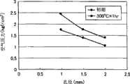
如图6所示,将薄板玻璃叠层体1设置于固定台50上,通过真空吸附固定,使薄板玻璃基板11为下侧。在此状态下,将压缩空气注入用的管子30的周围用密封剂40密封,使其与设置于支持用玻璃基板12上的孔14相连,使空气不会泄漏。之后,将1.41kgf/cm2(13.8×104Pa)的压缩空气通过孔14注入硅氧烷树脂层13和薄板玻璃基板11的界面,然后进行硅氧烷树脂层13和薄板玻璃基板11的剥离,可容易地用手将支持用玻璃基板12从薄板玻璃基板11分离。As shown in FIG. 6 , the thin-
对以300℃的温度加热1小时后的薄板玻璃叠层体1也实施相同步骤的处理。将1.75kgf/cm2(17.2×104Pa)的压缩空气通过孔14注入硅氧烷树脂层13和薄板玻璃基板11的界面,然后进行硅氧烷树脂层13和薄板玻璃基板11的剥离,可容易地用手将支持用玻璃基板12从薄板玻璃基板11分离。The treatment of the same procedure was implemented also about the sheet glass laminated
(实施例2、3)(Example 2, 3)
除将孔14的孔径变为1mm(实施例2)、2mm(实施例3)这一点以外,与实施例1相同实施处理。The processing was carried out in the same manner as in Example 1 except that the hole diameter of the
实施例1~3的剥离试验的结果如图7所示。由图7可以确认,如果增大孔14的孔径,则可降低分离薄板玻璃基板11和支持用玻璃基板12所需的压缩空气的压力。此外,以300℃的温度加热1小时后的薄板玻璃叠层体与加热前的薄板玻璃叠层体相比,虽有必要提高压缩空气的压力,但可以容易地用手将支持用玻璃基板12从薄板玻璃基板11分离。The results of the peeling test of Examples 1 to 3 are shown in FIG. 7 . It can be confirmed from FIG. 7 that the pressure of the compressed air required to separate the
(实施例4)(Example 4)
在纵向长度400mm、横向长度300mm、厚度0.7mm、线膨胀系数38×10-7/℃的支持用玻璃基板(旭硝子株式会社制AN100)的图8所示的规定的位置上用金刚石钻头开出7个孔径1.5mm的孔。用纯水清洗、UV清洗等将该基板净化后,用网板印刷机涂布100质量份的无溶剂加成反应型剥离纸用硅氧烷(信越有机硅株式会社制KNS—320A)和2质量份的铂系催化剂(信越有机硅株式会社制CAT-PL-56)的混合物(涂布量15g/m2),以100℃的温度在大气中加热固化3分钟,形成膜厚15μm的硅氧烷树脂层。在支持用玻璃基板上的孔的部分不形成硅氧烷树脂层,可形成连通支持用玻璃基板和硅氧烷树脂层的孔。Cut out with a diamond drill at the specified position shown in Figure 8 on a supporting glass substrate (AN100 manufactured by Asahi Glass Co., Ltd.) with a longitudinal length of 400 mm, a lateral length of 300 mm, a thickness of 0.7 mm, and a linear expansion coefficient of 38×10-7 /°C. 7 holes with a diameter of 1.5mm. After cleaning the substrate with pure water, UV cleaning, etc., 100 parts by mass of siloxane for solvent-free addition reaction type release paper (KNS-320A manufactured by Shin-Etsu Silicone Co., Ltd.) and 2 A mixture of platinum-based catalysts (Shin-Etsu Silicone Co., Ltd. CAT-PL-56) in parts by mass (coating amount: 15 g/m2 ) was heated and cured at 100°C in the air for 3 minutes to form silicon with a film thickness of 15 µm. oxane resin layer. The silicone resin layer is not formed in the portion of the hole in the glass substrate for support, and a hole communicating the glass substrate for support and the silicone resin layer may be formed.
用纯水清洗、UV清洗等将纵向长度400mm、横向长度300mm、厚度0.1mm、线膨胀系数38×10-7/℃的薄板玻璃基板(旭硝子株式会社制AN100)的与硅氧烷树脂层的接触侧的面净化后,在室温下用真空加压将支持用玻璃基板的硅氧烷树脂层形成面与薄板玻璃基板贴合,得到本发明的薄板玻璃叠层体(薄板玻璃叠层体2)。A thin glass substrate (AN100 manufactured by Asahi Glass Co., Ltd.) with a vertical length of 400 mm, a horizontal length of 300 mm, a thickness of 0.1 mm, and a coefficient of linear expansion of 38×10-7 /°C and a silicone resin layer were washed with pure water or UV. After cleaning the surface on the contact side, the siloxane resin layer forming surface of the supporting glass substrate and the thin glass substrate were bonded together under vacuum pressure at room temperature to obtain the thin-plate glass laminate of the present invention (thin-plate glass laminate 2 ).
薄板玻璃叠层体2中,薄板玻璃基板在不产生气泡的情况下与硅氧烷树脂层密合,也无凸状缺陷,平滑性也良好。In the thin-
[剥离试验][Peel test]
将薄板玻璃叠层体2设置于具有多个微细的吸附孔的平滑的固定台上,通过真空吸附固定,使薄板玻璃基板为下侧。在此状态下,将压缩空气注入用的管子的周围用密封剂密封,使其与形成于支持用玻璃基板上的各孔相连,使空气不会泄漏。之后,将3.5×10⁴Pa的压缩空气通过设置于支持用玻璃基板上的孔注入硅氧烷树脂层和薄板玻璃基板的界面,然后进行硅氧烷树脂层和薄板玻璃基板的剥离,可容易地用手将支持用玻璃基板从薄板玻璃基板分离。The
(实施例5)(Example 5)
本实施例中,用实施例4中得到的薄板玻璃叠层体2制造LCD。准备2块薄板玻璃叠层体2,对1块实施阵列形成工序,在薄板玻璃基板的表面形成阵列。对剩下的1块实施滤色片形成工序,在薄板玻璃基板的表面形成滤色片。将形成有阵列的薄板玻璃基板与形成有滤色片的薄板玻璃基板贴合后,用使用图5(a)、(b)进行说明的方法将2块支持用玻璃基板分离。接着,用激光切割器切割薄板玻璃基板,分割成28个纵向长度51mm×横向长度38mm的单元,之后实施液晶注入工序及注入口的密封工序,形成液晶单元。实施在形成的液晶单元上贴附偏光板的工序,接着实施模块形成工序,得到LCD。如上所述得到的LCD未产生特性方面的问题。In this example, an LCD was manufactured using the thin
(实施例6)(Example 6)
本实施例中,用实施例4中得到的薄板玻璃叠层体2和厚度0.7mm的无碱玻璃基板制造LCD。准备薄板玻璃叠层体2,实施滤色片形成工序,在薄板玻璃基板的表面形成滤色片。另一方面,对厚度0.7mm的无碱玻璃基板(旭硝子株式会社制AN100)实施阵列形成工序,在厚度0.7mm的无碱玻璃基板的表面形成阵列。In this example, an LCD was produced using the
将形成有滤色片的薄板玻璃基板与形成有阵列的厚度0.7mm的无碱玻璃基板贴合后,用使用图5(a)、(b)进行说明的方法将支持用玻璃基板分离。After laminating the thin glass substrate on which the color filters were formed and the 0.7 mm thick non-alkali glass substrate on which the array was formed, the supporting glass substrate was separated by the method described with reference to FIGS. 5( a ) and ( b ).
接着,将薄板玻璃基板—无碱玻璃基板贴合体分割成28个纵向长度51mm×横向长度38mm的单元,此时,用激光切割器切割薄板玻璃基板。另一方面,用激光切割器或划线裂片(scribe-break)法切割无碱玻璃基板。Next, the thin glass substrate-alkali-free glass substrate bonded body was divided into 28 units with a vertical length of 51 mm×a horizontal length of 38 mm, and at this time, the thin glass substrate was cut with a laser cutter. On the other hand, the non-alkali glass substrate is cut with a laser cutter or a scribe-break method.
之后,实施液晶注入工序及注入口的密封工序,形成液晶单元。实施在形成的液晶单元上贴附偏光板的工序,接着实施模块形成工序,得到LCD。如上所述得到的LCD未产生特性方面的问题。Thereafter, a liquid crystal injection step and an injection port sealing step are implemented to form a liquid crystal cell. A step of attaching a polarizing plate to the formed liquid crystal cell is performed, and then a module forming step is performed to obtain an LCD. The LCD obtained as described above did not cause any problems in characteristics.
(实施例7)(Example 7)
本实施例中,用实施例4中得到的薄板玻璃叠层体2制造OLED。实施形成透明电极的工序,形成辅助电极的工序,蒸镀空穴注入层、空穴传输层、发光层、电子传输层等的工序,将它们密封的工序,藉此在薄板玻璃叠层体2的薄板玻璃基板上形成有机EL结构体。接着,用实施例4中记载的方法将薄板玻璃基板和支持用玻璃基板分离。接着,用激光切割器切割薄板玻璃基板,分割成40个纵向长度41mm×横向长度30mm的单元,之后将形成有有机EL结构体的薄板玻璃基板和对向基板装配起来,实施模块形成工序,制成OLED。如上所述得到的OLED未产生特性方面的问题。In this example, an OLED was produced using the
(比较例1)(comparative example 1)
除使用未开孔的支持用玻璃基板外,实施与实施例4相同步骤的处理,得到比较例的薄板玻璃叠层体3。薄板玻璃叠层体3中,为剥离支持用玻璃基板,必需用剃刀刀刃赋予端部以剥离的切入点,支持用玻璃基板的分离需要相当多的时间。Except having used the support glass substrate which did not perforate, the same procedure as Example 4 was implemented, and the thin-plate glass laminated
产业上利用的可能性Possibility of industrial use
利用本发明得到的薄板玻璃叠层体,可在LCD、OLED等各种显示装置的制造工序内作为显示装置用玻璃基板的处理用的薄板玻璃叠层体使用。此外,使用了本发明的薄板玻璃叠层体的显示装置的制造方法可作为LCD、OLED等各种显示装置的制造方法使用。The sheet glass laminate obtained by the present invention can be used as a sheet glass laminate for processing glass substrates for display devices in the production process of various display devices such as LCDs and OLEDs. In addition, the method of manufacturing a display device using the sheet glass laminate of the present invention can be used as a method of manufacturing various display devices such as LCDs and OLEDs.
这里引用2006年5月8日提出申请的日本专利申请2006-129282号的说明书、权利要求书、附图以及摘要的全部内容作为本发明的说明书的揭示。The specification, claims, drawings, and abstract of Japanese Patent Application No. 2006-129282 filed on May 8, 2006 are cited here as disclosure of the specification of the present invention.
Claims (15)
Applications Claiming Priority (3)
| Application Number | Priority Date | Filing Date | Title |
|---|---|---|---|
| JP129282/2006 | 2006-05-08 | ||
| JP2006129282 | 2006-05-08 | ||
| PCT/JP2007/058655WO2007129554A1 (en) | 2006-05-08 | 2007-04-20 | Thin-sheet glass laminate, process for manufacturing display apparatus using the laminate, and supporting glass substrate |
Publications (2)
| Publication Number | Publication Date |
|---|---|
| CN101437772A CN101437772A (en) | 2009-05-20 |
| CN101437772Btrue CN101437772B (en) | 2011-09-07 |
Family
ID=38667662
Family Applications (1)
| Application Number | Title | Priority Date | Filing Date |
|---|---|---|---|
| CN2007800163971AExpired - Fee RelatedCN101437772B (en) | 2006-05-08 | 2007-04-20 | Thin plate glass laminate, process for producing display device using thin plate glass laminate, and support glass substrate |
Country Status (6)
| Country | Link |
|---|---|
| US (1) | US8157945B2 (en) |
| EP (1) | EP2025650A1 (en) |
| KR (1) | KR20090006824A (en) |
| CN (1) | CN101437772B (en) |
| TW (1) | TWI394722B (en) |
| WO (1) | WO2007129554A1 (en) |
Families Citing this family (66)
| Publication number | Priority date | Publication date | Assignee | Title |
|---|---|---|---|---|
| US7776656B2 (en)* | 2005-07-29 | 2010-08-17 | Semiconductor Energy Laboratory Co., Ltd. | Method for manufacturing semiconductor device |
| JP5532918B2 (en) | 2007-03-12 | 2014-06-25 | 旭硝子株式会社 | Method for manufacturing display device using glass substrate with protective glass |
| US8179127B2 (en)* | 2007-11-06 | 2012-05-15 | GM Global Technology Operations LLC | Method and apparatus to monitor position of a rotatable shaft |
| JP5308718B2 (en) | 2008-05-26 | 2013-10-09 | 浜松ホトニクス株式会社 | Glass welding method |
| JP5535652B2 (en) | 2008-06-11 | 2014-07-02 | 浜松ホトニクス株式会社 | Glass welding method |
| DE112009001456T5 (en) | 2008-06-23 | 2011-05-19 | Hamamatsu Photonics K.K., Hamamatsu-shi | Glass fusing method |
| WO2010047273A1 (en)* | 2008-10-23 | 2010-04-29 | 旭硝子株式会社 | Glass substrate laminated device and method for producing laminate glass substrate |
| US9063605B2 (en)* | 2009-01-09 | 2015-06-23 | Apple Inc. | Thin glass processing using a carrier |
| US8697228B2 (en) | 2009-05-06 | 2014-04-15 | Corning Incorporated | Carrier for glass substrates |
| JP5594522B2 (en)* | 2009-07-03 | 2014-09-24 | 日本電気硝子株式会社 | Glass film laminate for manufacturing electronic devices |
| JP5733600B2 (en)* | 2009-07-03 | 2015-06-10 | 日本電気硝子株式会社 | Device sealing body manufacturing method and element sealing body |
| EP2479151B1 (en)* | 2009-09-18 | 2020-10-28 | Nippon Electric Glass Co., Ltd. | Method for producing glass film, method for processing glass film, and glass film laminate |
| WO2011048979A1 (en)* | 2009-10-20 | 2011-04-28 | 旭硝子株式会社 | Glass laminate, glass laminate manufacturing method, display panel manufacturing method, and display panel obtained by means of display panel manufacturing method |
| JP5481167B2 (en)* | 2009-11-12 | 2014-04-23 | 浜松ホトニクス株式会社 | Glass welding method |
| JP5481172B2 (en) | 2009-11-25 | 2014-04-23 | 浜松ホトニクス株式会社 | Glass welding method and glass layer fixing method |
| JP5567319B2 (en) | 2009-11-25 | 2014-08-06 | 浜松ホトニクス株式会社 | Glass welding method and glass layer fixing method |
| JP5535590B2 (en) | 2009-11-25 | 2014-07-02 | 浜松ホトニクス株式会社 | Glass welding method and glass layer fixing method |
| JP5525246B2 (en) | 2009-11-25 | 2014-06-18 | 浜松ホトニクス株式会社 | Glass welding method and glass layer fixing method |
| JP5535588B2 (en) | 2009-11-25 | 2014-07-02 | 浜松ホトニクス株式会社 | Glass welding method and glass layer fixing method |
| JP5466929B2 (en) | 2009-11-25 | 2014-04-09 | 浜松ホトニクス株式会社 | Glass welding method and glass layer fixing method |
| JP5535589B2 (en) | 2009-11-25 | 2014-07-02 | 浜松ホトニクス株式会社 | Glass welding method and glass layer fixing method |
| JP5481173B2 (en) | 2009-11-25 | 2014-04-23 | 浜松ホトニクス株式会社 | Glass welding method and glass layer fixing method |
| KR20130097069A (en)* | 2010-05-11 | 2013-09-02 | 아사히 가라스 가부시키가이샤 | Process for producing laminate, and laminate |
| US9333724B2 (en) | 2010-07-28 | 2016-05-10 | Nippon Electric Glass Co., Ltd. | Glass film laminate |
| KR101237617B1 (en)* | 2010-09-07 | 2013-02-26 | 삼성전기주식회사 | Exposure apparatus for substrate |
| CN102548758B (en)* | 2011-02-01 | 2013-11-20 | 株式会社微龙技术研究所 | Thin-sheet glass substrate laminate and method of manufacturing the same |
| CN104691058B (en) | 2011-05-13 | 2016-09-28 | 日本电气硝子株式会社 | Duplexer, the cutting-off method of duplexer and the processing method of duplexer and the shearing device of fragility plate object and cutting-off method |
| CN102825912B (en)* | 2011-06-14 | 2015-11-25 | 研能科技股份有限公司 | Orifice sheet structure |
| CN103619536B (en)* | 2011-06-23 | 2016-06-01 | 旭硝子株式会社 | Manufacturing method of laminated body |
| WO2013058217A1 (en)* | 2011-10-18 | 2013-04-25 | 旭硝子株式会社 | Laminate, method for producing laminate, and method for producing glass substrate having member for electronic devices attached thereto |
| US10543662B2 (en) | 2012-02-08 | 2020-01-28 | Corning Incorporated | Device modified substrate article and methods for making |
| JP5822075B2 (en)* | 2012-02-15 | 2015-11-24 | 日本電気硝子株式会社 | Method for producing roll-shaped thin glass plate laminate |
| KR101941448B1 (en)* | 2012-02-29 | 2019-01-23 | 엘지디스플레이 주식회사 | Method of fabricating lightweight and thin liquid crystal display device |
| KR101970553B1 (en)* | 2012-05-23 | 2019-08-13 | 엘지디스플레이 주식회사 | Method of fabricating lightweight and thin liquid crystal display device |
| WO2013176146A1 (en)* | 2012-05-24 | 2013-11-28 | 旭硝子株式会社 | Manufacturing method for optical member, optical member, optical member having protective film, and manufacturing method for optical panel |
| US10014177B2 (en) | 2012-12-13 | 2018-07-03 | Corning Incorporated | Methods for processing electronic devices |
| US10086584B2 (en)* | 2012-12-13 | 2018-10-02 | Corning Incorporated | Glass articles and methods for controlled bonding of glass sheets with carriers |
| TWI617437B (en) | 2012-12-13 | 2018-03-11 | 康寧公司 | Facilitated processing for controlling bonding between sheet and carrier |
| US9340443B2 (en) | 2012-12-13 | 2016-05-17 | Corning Incorporated | Bulk annealing of glass sheets |
| TWI588079B (en)* | 2013-03-06 | 2017-06-21 | 友達光電股份有限公司 | Method for separating flexible plate from bearing plate |
| WO2014151353A1 (en)* | 2013-03-15 | 2014-09-25 | Corning Incorporated | Bulk annealing of glass sheets |
| WO2014201665A1 (en) | 2013-06-20 | 2014-12-24 | Schott Glass Technologies (Suzhou) Co. Ltd. | Bonded article of thin glass on support substrate, preparation method and use thereof |
| CN103331983B (en)* | 2013-06-24 | 2015-11-04 | 句容骏成电子有限公司 | A kind of hot-press method |
| KR20150001006A (en) | 2013-06-26 | 2015-01-06 | 삼성디스플레이 주식회사 | Glass film laminate, method of manufacturing the same, and method of manufacturing glass film |
| KR101493396B1 (en)* | 2013-07-26 | 2015-02-13 | 코닝정밀소재 주식회사 | Method of ultra handling thin glass for display panel |
| US10510576B2 (en) | 2013-10-14 | 2019-12-17 | Corning Incorporated | Carrier-bonding methods and articles for semiconductor and interposer processing |
| CN106132688B (en) | 2014-01-27 | 2020-07-14 | 康宁股份有限公司 | Article and method for controlled bonding of a sheet to a carrier |
| KR102049612B1 (en) | 2014-03-13 | 2019-11-27 | 도쿠슈 도카이 세이시 가부시키가이샤 | Glass interleaving paper |
| EP3129221A1 (en) | 2014-04-09 | 2017-02-15 | Corning Incorporated | Device modified substrate article and methods for making |
| JP2015211162A (en)* | 2014-04-28 | 2015-11-24 | 旭硝子株式会社 | Method for manufacturing glass member, glass member, and glass interposer |
| US10479052B2 (en) | 2014-08-20 | 2019-11-19 | Corning Incorporated | Methods of forming shaped glass articles from glass sheets |
| CN104261133B (en)* | 2014-09-10 | 2017-04-12 | 林嘉佑 | Glass deep-processing automatic producing device and method thereof |
| SG11201707090YA (en) | 2015-03-04 | 2017-09-28 | Corning Inc | Methods and apparatus for initiating debonding between two sheets of an assembly |
| EP3297824A1 (en)* | 2015-05-19 | 2018-03-28 | Corning Incorporated | Articles and methods for bonding sheets with carriers |
| KR101708317B1 (en)* | 2015-06-17 | 2017-02-20 | 엘지전자 주식회사 | Strain inspection device and attaching method thereof |
| KR102524620B1 (en) | 2015-06-26 | 2023-04-21 | 코닝 인코포레이티드 | Methods and articles including sheets and carriers |
| CN106739424B (en) | 2015-11-20 | 2020-02-14 | 财团法人工业技术研究院 | Taking-down and bonding device, taking-down method and bonding method using same |
| CN106793488B (en) | 2015-11-20 | 2019-04-30 | 财团法人工业技术研究院 | Flexible electronic device and manufacturing process method thereof |
| TW201737766A (en) | 2016-01-21 | 2017-10-16 | 康寧公司 | Methods for processing a substrate |
| TW201825623A (en) | 2016-08-30 | 2018-07-16 | 美商康寧公司 | Peptide plasma polymer for sheet bonding |
| TWI821867B (en) | 2016-08-31 | 2023-11-11 | 美商康寧公司 | Articles of controllably bonded sheets and methods for making same |
| TWI629128B (en)* | 2016-12-09 | 2018-07-11 | 財團法人金屬工業研究發展中心 | Induction electrochemical machining device and machining method |
| WO2018181393A1 (en)* | 2017-03-29 | 2018-10-04 | 日本ゼオン株式会社 | Laminate and manufacturing method of organic solar battery |
| JP7260523B2 (en) | 2017-08-18 | 2023-04-18 | コーニング インコーポレイテッド | Temporary binding using polycationic polymers |
| US11331692B2 (en) | 2017-12-15 | 2022-05-17 | Corning Incorporated | Methods for treating a substrate and method for making articles comprising bonded sheets |
| CN110783393B (en)* | 2019-11-15 | 2022-03-08 | 昆山国显光电有限公司 | Display panel protection structure and display assembly |
Citations (2)
| Publication number | Priority date | Publication date | Assignee | Title |
|---|---|---|---|---|
| CN1213356A (en)* | 1997-01-13 | 1999-04-07 | 日本板硝子株式会社 | Manufacturing method of laminated glass |
| CN1406769A (en)* | 2001-08-30 | 2003-04-02 | 乔治·威廉·乔伯 | A laminated decorative glass plate and its manufacturing method |
Family Cites Families (13)
| Publication number | Priority date | Publication date | Assignee | Title |
|---|---|---|---|---|
| JPS5854316A (en) | 1981-09-25 | 1983-03-31 | Sharp Corp | Production for liquid crystal display device |
| JP3081122B2 (en) | 1994-07-18 | 2000-08-28 | シャープ株式会社 | Jig for transporting substrate and method of manufacturing liquid crystal display element using the same |
| JP3203166B2 (en) | 1995-10-13 | 2001-08-27 | シャープ株式会社 | Jig for manufacturing liquid crystal display element and method for manufacturing liquid crystal display element using the same |
| US6287674B1 (en)* | 1997-10-24 | 2001-09-11 | Agfa-Gevaert | Laminate comprising a thin borosilicate glass substrate as a constituting layer |
| US5985396A (en)* | 1997-11-25 | 1999-11-16 | Kimberly-Clark Worldwide, Inc. | Flushable release liners and methods of making the same |
| JP3202718B2 (en) | 1999-02-23 | 2001-08-27 | 鹿児島日本電気株式会社 | Display device manufacturing jig and display device manufacturing method using the same |
| JP2000252342A (en) | 1999-03-01 | 2000-09-14 | Seiko Epson Corp | Method of transporting thin plate and method of manufacturing liquid crystal panel |
| JP2003288028A (en)* | 2001-12-25 | 2003-10-10 | Canon Inc | Image display device disassembling method, image display device manufacturing method, support body manufacturing method, image display unit manufacturing method, processed material manufacturing method, and image display device |
| JP2003216068A (en) | 2002-01-28 | 2003-07-30 | Matsushita Electric Ind Co Ltd | Display device and substrate for display device, and method of manufacturing the same |
| JP4619710B2 (en)* | 2004-07-02 | 2011-01-26 | 東レ・ダウコーニング株式会社 | Silicone pressure sensitive adhesive and adhesive tape |
| JP4534719B2 (en) | 2004-10-29 | 2010-09-01 | 株式会社富士通ゼネラル | Gateway device |
| KR101285442B1 (en) | 2005-08-09 | 2013-07-12 | 아사히 가라스 가부시키가이샤 | Thin sheet glass laminate and method for manufacturing display using thin sheet glass laminate |
| JPWO2007023534A1 (en)* | 2005-08-24 | 2009-02-26 | 日立プラズマディスプレイ株式会社 | Display panel device |
- 2007
- 2007-04-20CNCN2007800163971Apatent/CN101437772B/ennot_activeExpired - Fee Related
- 2007-04-20WOPCT/JP2007/058655patent/WO2007129554A1/enactiveApplication Filing
- 2007-04-20EPEP20070742090patent/EP2025650A1/ennot_activeWithdrawn
- 2007-04-20KRKR1020087022147Apatent/KR20090006824A/ennot_activeAbandoned
- 2007-04-27TWTW96115112Apatent/TWI394722B/ennot_activeIP Right Cessation
- 2008
- 2008-11-07USUS12/267,029patent/US8157945B2/ennot_activeExpired - Fee Related
Patent Citations (2)
| Publication number | Priority date | Publication date | Assignee | Title |
|---|---|---|---|---|
| CN1213356A (en)* | 1997-01-13 | 1999-04-07 | 日本板硝子株式会社 | Manufacturing method of laminated glass |
| CN1406769A (en)* | 2001-08-30 | 2003-04-02 | 乔治·威廉·乔伯 | A laminated decorative glass plate and its manufacturing method |
Non-Patent Citations (2)
| Title |
|---|
| JP特开2003-288028A 2003.10.10 |
| JP特开平9-105896A 1997.04.22 |
Also Published As
| Publication number | Publication date |
|---|---|
| US8157945B2 (en) | 2012-04-17 |
| TW200744965A (en) | 2007-12-16 |
| KR20090006824A (en) | 2009-01-15 |
| WO2007129554A1 (en) | 2007-11-15 |
| TWI394722B (en) | 2013-05-01 |
| CN101437772A (en) | 2009-05-20 |
| EP2025650A1 (en) | 2009-02-18 |
| US20090110882A1 (en) | 2009-04-30 |
Similar Documents
| Publication | Publication Date | Title |
|---|---|---|
| CN101437772B (en) | Thin plate glass laminate, process for producing display device using thin plate glass laminate, and support glass substrate | |
| JP4930161B2 (en) | Thin glass laminated body, display device manufacturing method using thin glass laminated body, and supporting glass substrate | |
| CN101242951B (en) | Sheet glass laminate and method of manufacturing display device using the sheet glass laminate | |
| CN101626991B (en) | Glass substrate provided with protection glass and method for manufacturing display device using glass substrate provided with protection glass | |
| US8303754B2 (en) | Glass substrate with protective glass, process for producing display device using glass substrate with protective glass, and silicone for release paper | |
| KR101670098B1 (en) | Glass substrate laminated device and method for producing laminate glass substrate | |
| WO2011024690A1 (en) | Multilayer structure with flexible base material and support, panel for use in electronic device provided with support and production method for panel for use in electronic device | |
| KR20140079783A (en) | Laminate, method for producing laminate, and method for producing glass substrate having member for electronic devices attached thereto | |
| CN104903095B (en) | Glass laminate, manufacturing method thereof, and support substrate with silicone resin layer | |
| CN103435257B (en) | Glass film layers lamination and manufacture method thereof | |
| CN104736340B (en) | Glass laminate and its manufacture method and the supporting base material with silicone layer | |
| TW201420335A (en) | Glass laminate and manufacturing method for same, and support substrate having silicone resin layer attached thereto and manufacturing method for same | |
| CN105432147B (en) | The manufacture method of electronic equipment | |
| TWI656967B (en) | Glass laminated body, manufacturing method thereof, and manufacturing method of electronic device |
Legal Events
| Date | Code | Title | Description |
|---|---|---|---|
| C06 | Publication | ||
| PB01 | Publication | ||
| C10 | Entry into substantive examination | ||
| SE01 | Entry into force of request for substantive examination | ||
| C14 | Grant of patent or utility model | ||
| GR01 | Patent grant | ||
| CF01 | Termination of patent right due to non-payment of annual fee | ||
| CF01 | Termination of patent right due to non-payment of annual fee | Granted publication date:20110907 Termination date:20180420 |