CN101436393B - Light-emitting diode backlight module and its driving circuit and method - Google Patents
Light-emitting diode backlight module and its driving circuit and methodDownload PDFInfo
- Publication number
- CN101436393B CN101436393BCN2008101852732ACN200810185273ACN101436393BCN 101436393 BCN101436393 BCN 101436393BCN 2008101852732 ACN2008101852732 ACN 2008101852732ACN 200810185273 ACN200810185273 ACN 200810185273ACN 101436393 BCN101436393 BCN 101436393B
- Authority
- CN
- China
- Prior art keywords
- emitting diode
- control
- backlight
- driving circuit
- light
- Prior art date
- Legal status (The legal status is an assumption and is not a legal conclusion. Google has not performed a legal analysis and makes no representation as to the accuracy of the status listed.)
- Active
Links
- 238000000034methodMethods0.000titleclaimsabstractdescription24
- 239000011159matrix materialSubstances0.000claimsdescription5
- 238000004020luminiscence typeMethods0.000claims6
- 230000005540biological transmissionEffects0.000abstractdescription12
- 238000004519manufacturing processMethods0.000abstractdescription6
- 239000004973liquid crystal related substanceSubstances0.000description23
- 230000000630rising effectEffects0.000description16
- 238000010586diagramMethods0.000description9
- 238000005192partitionMethods0.000description4
- 230000007423decreaseEffects0.000description2
- 238000012986modificationMethods0.000description2
- 230000004048modificationEffects0.000description2
- 238000005516engineering processMethods0.000description1
- 238000005286illuminationMethods0.000description1
- 230000005855radiationEffects0.000description1
- 239000004065semiconductorSubstances0.000description1
Images


Landscapes
- Control Of Indicators Other Than Cathode Ray Tubes (AREA)
- Liquid Crystal Display Device Control (AREA)
Abstract
Description
Translated fromChinese技术领域technical field
本发明涉及一种背光模块,且特别涉及一种发光二极管背光模块及其驱动电路与方法。The invention relates to a backlight module, and in particular to a light emitting diode backlight module and its driving circuit and method.
背景技术Background technique
近年来,随着半导体科技蓬勃发展,便携式电子产品及平面显示器产品也随之兴起。而在众多平面显示器的类型当中,液晶显示器(Liquid CrystalDisplay,LCD)基于其低电压操作、无辐射线散射、重量轻以及体积小等优点,随即已成为显示器产品的主流。In recent years, with the vigorous development of semiconductor technology, portable electronic products and flat panel display products are also emerging. Among the types of flat panel displays, Liquid Crystal Display (LCD) has become the mainstream of display products due to its advantages of low voltage operation, no radiation scattering, light weight and small size.
一般而言,由于液晶显示面板并不具备自发光的特性,因此必须在液晶显示面板的下方放置背光模块,借以提供液晶显示面板所需的光源。传统的背光模块大致可以分为两类,其一为由冷阴极管(cold cathode FluorescentLamps,CCFL)所组成的背光模块,而另一则为由发光二极管(light emittingdiode,LED)所组成的背光模块。其中,由于发光二极管背光模块可以提升液晶显示器的色域,故而现今各家厂商大多以发光二极管背光模块来取代冷阴极管背光模块。Generally speaking, since the liquid crystal display panel does not have the characteristic of self-illumination, a backlight module must be placed under the liquid crystal display panel to provide the light source required by the liquid crystal display panel. Traditional backlight modules can be roughly divided into two categories, one is a backlight module composed of cold cathode fluorescent lamps (CCFL), and the other is a backlight module composed of light emitting diodes (light emitting diodes, LEDs). . Among them, since the LED backlight module can improve the color gamut of the liquid crystal display, most manufacturers now replace the cold-cathode tube backlight module with the LED backlight module.
然而,由于现今驱动发光二极管背光模块的方式大多采用脉冲宽度调制(pulse width modulation,PWM)与分区控制的概念,故而当分区控制的区域数增加时,可能会造成以下几点缺点:However, since most of the current methods of driving LED backlight modules adopt the concepts of pulse width modulation (PWM) and partition control, when the number of zones controlled by partitions increases, the following disadvantages may occur:
1、传输线与传输时间大幅地增加;1. The transmission line and transmission time are greatly increased;
2、PWM的控制方式较没有弹性;以及2. The PWM control method is less flexible; and
3、每一分区控制的区域内皆必须配置一个电流控制器,故而会大幅地增加制作成本。3. A current controller must be installed in the area controlled by each partition, so the production cost will be greatly increased.
发明内容Contents of the invention
有鉴于此,本发明提供一种发光二极管背光模块及其驱动电路与方法,借以减少传输线与传输时间、增加PWM的控制方式的弹性,并且采用定电压控制的方式来降低制作成本。In view of this, the present invention provides an LED backlight module and its driving circuit and method, thereby reducing the transmission line and transmission time, increasing the flexibility of the PWM control method, and reducing the production cost by adopting the constant voltage control method.
本发明提供一种驱动电路,其适于驱动液晶显示器的发光二极管背光模块内的至少一区发光单元中的至少一发光二极管。本发明所提出的驱动电路包括闩锁单元与开关单元。其中,闩锁单元用以接收一控制背光数据,并依据一触发信号而于一画面期间内对所述控制背光数据进行闩锁,借以输出一控制信号。开关单元耦接闩锁单元与发光二极管,用以接收所述控制信号,并据以决定发光二极管是否发光。The invention provides a driving circuit, which is suitable for driving at least one light emitting diode in at least one area light emitting unit in a light emitting diode backlight module of a liquid crystal display. The driving circuit proposed by the present invention includes a latch unit and a switch unit. Wherein, the latch unit is used for receiving backlight control data, and latching the backlight control data within a frame period according to a trigger signal, so as to output a control signal. The switch unit is coupled to the latch unit and the LED to receive the control signal and determine whether the LED emits light or not.
本发明另提供一种驱动方法,其适于驱动一发光二极管背光模块内的至少一区发光单元中的至少一发光二极管。本发明所提出的驱动方法包括:首先,提供一控制背光数据与一触发信号;接着,依据该触发信号而于一画面期间内对该控制背光数据进行闩锁,借以输出一控制信号;最后,依据所述控制信号以驱动发光二极管。The present invention further provides a driving method, which is suitable for driving at least one light emitting diode in at least one area of light emitting units in a light emitting diode backlight module. The driving method proposed by the present invention includes: firstly, providing a control backlight data and a trigger signal; then, according to the trigger signal, latching the control backlight data within a frame period, so as to output a control signal; finally, The LED is driven according to the control signal.
本发明另提供一种具有上述本发明所提出的驱动电路的发光二极管背光模块。The present invention further provides an LED backlight module having the driving circuit proposed by the present invention.
本发明将驱动发光二极管背光模块的每一分区控制的区域内所需的驱动电路排列成矩阵结构,并且以快速扫描的方式来提供触发信号以控制每一区发光单元的发光二极管串,如此设计方式即可以大量减少传输线与传输时间。另外,由于每一驱动电路内又具有闩锁单元以对控制背光数据进行闩锁,所以在快速扫描以提供触发信号来控制每一区发光单元的发光二极管串的同时,并不让每一区发光单元的发光二极管串亮度降低或发生闪烁。每个分区控制的区域中并不需使用电流控制器,如此一来即可大大地将低制作成本。适应性地改变由背光控制器或时序控制器所提供的控制背光数据后,即可大幅地增加PWM的控制方式的弹性。In the present invention, the drive circuits required to drive the LED backlight module in each area controlled by each area are arranged in a matrix structure, and a trigger signal is provided in a fast scanning manner to control the LED strings of the light-emitting units in each area, so designed In this way, the transmission line and transmission time can be greatly reduced. In addition, because there is a latch unit in each driving circuit to latch the control backlight data, so while fast scanning is used to provide a trigger signal to control the light-emitting diode strings of the light-emitting units in each region, each region does not The brightness of the light emitting diode strings of the light emitting unit decreases or flickers. The area controlled by each partition does not need to use a current controller, so that the manufacturing cost can be greatly reduced. After adaptively changing the backlight control data provided by the backlight controller or the timing controller, the flexibility of the PWM control method can be greatly increased.
为让本发明的上述和其他目的、特征和优点能更明显易懂,下文特举本发明几个优选实施例,并配合附图,作详细说明如下。In order to make the above and other objects, features and advantages of the present invention more comprehensible, several preferred embodiments of the present invention will be described in detail below together with the accompanying drawings.
附图说明Description of drawings
图1示出本发明一优选实施例的液晶显示器的方块图。FIG. 1 shows a block diagram of a liquid crystal display of a preferred embodiment of the present invention.
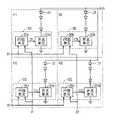
图2示出本发明一优选实施例的发光二极管背光模块的电路示意图。FIG. 2 shows a schematic circuit diagram of an LED backlight module according to a preferred embodiment of the present invention.
图3示出本发明一优选实施例的每一闩锁单元的电路图。FIG. 3 shows a circuit diagram of each latch unit in a preferred embodiment of the present invention.
图4示出本发明一优选实施例的每一开关单元的电路图。FIG. 4 shows a circuit diagram of each switch unit in a preferred embodiment of the present invention.
图5示出本发明一优选实施例的每一驱动电路的操作时序图。FIG. 5 shows an operation timing diagram of each driving circuit in a preferred embodiment of the present invention.
图6示出本发明一优选实施例的驱动方法流程图。Fig. 6 shows a flowchart of a driving method in a preferred embodiment of the present invention.
上述附图中的附图标记说明如下:The reference numerals in the above-mentioned accompanying drawings are explained as follows:
100:液晶显示器100: LCD display
101:液晶显示面板101: Liquid crystal display panel
103:发光二极管背光模块103: LED backlight module
105:时序控制器105: Timing controller
107:栅极驱动器107: Gate driver
109:源极驱动器109: Source driver
111:背光控制器111: Backlight controller
201a~201d:闩锁单元201a-201d: latch unit
203a~203d:开关单元203a~203d: switch unit
301:D型触发器301: D-Type Flip-Flop
401:N型晶体管401: N-type transistor
A11、A12、A21、A22:发光单元A11, A12, A21, A22: light emitting unit
D11、D12、D21、D22:驱动电路D11, D12, D21, D22: drive circuit
L11、L12、L21、L22:发光二极管串L11, L12, L21, L22: LED strings
C11、C12、C21、C22:控制信号C11, C12, C21, C22: control signal
A1、A2:控制背光数据A1, A2: control backlight data
B1、B2:触发信号B1, B2: trigger signal
F:画面期间F: during the screen
D:数据接收端D: data receiving end
CK:时钟脉冲输入端CK: clock pulse input
Q:数据输出端Q: data output terminal
Vs:系统电压Vs: system voltage
t1~t8:时间t1~t8: time
S601~S605:本发明一优选实施例的驱动方法流程图各步骤S601~S605: each step of the flow chart of the driving method in a preferred embodiment of the present invention
具体实施方式Detailed ways
图1示出本发明一优选实施例的液晶显示器100的方块图。请参照图1,液晶显示器100包括液晶显示面板101、发光二极管背光模块103、时序控制器105、栅极驱动器107、源极驱动器109,以及背光控制器111。其中,栅极驱动器107与源极驱动器109受控于时序控制器105,用以分别提供扫描信号与显示信号以驱动液晶显示面板101内的像素。FIG. 1 shows a block diagram of a
于本优选实施例中,发光二极管背光模块103具有4区发光单元A11、A12、A21与A22(但并不限制于此),每一区发光单元A11、A12、A21与A22皆受控于背光控制器111,用以分别提供光源给对应的液晶显示面板101的像素区域。In this preferred embodiment, the
进一步来说,图2示出本发明一优选实施例的发光二极管背光模块103的电路示意图。请合并参照图1与图2,每一区发光单元A11、A12、A21与A22皆具有多颗串接在一起的发光二极管与一个驱动电路。也即:发光单元A11具有多颗串接在一起的发光二极管L11(以下称为发光二极管串L11)以及驱动电路D11。发光单元A12具有多颗串接在一起的发光二极管L12(以下称为发光二极管串L12)以及驱动电路D12。发光单元A21具有多颗串接在一起的发光二极管L21(以下称为发光二极管串L21)以及驱动电路D21。发光单元A22具有多颗串接在一起的发光二极管L22(以下称为发光二极管串L22)以及驱动电路D22。Further, FIG. 2 shows a schematic circuit diagram of an
于本优选实施例中,发光单元A11的驱动电路D11具有闩锁单元201a与开关单元203a。其中,闩锁单元201a用以接收由背光控制器111所提供的控制背光数据A1,并依据背光控制器111所提供的触发信号B1,而于液晶显示器100的一个画面期间(frame period)内对控制背光数据A1进行闩锁,借以输出控制信号C11。开关单元203a耦接闩锁单元201a与发光二极管L11,用以接收闩锁单元201a所输出的控制信号C11,并据以决定发光二极管串L11是否发光。In this preferred embodiment, the driving circuit D11 of the light emitting unit A11 has a latch unit 201a and a switch unit 203a. Wherein, the latch unit 201a is used for receiving the control backlight data A1 provided by the
发光单元A21的驱动电路D21具有闩锁单元201b与开关单元203b。其中,闩锁单元201b用以接收由背光控制器111所提供的控制背光数据A2,并依据背光控制器111所提供的触发信号B1,而于液晶显示器100的一个画面期间内对控制背光数据A2进行闩锁,借以输出控制信号C21。开关单元203b耦接闩锁单元201b与发光二极管L21,用以接收闩锁单元201b所输出的控制信号C21,并据以决定发光二极管串L21是否发光。The driving circuit D21 of the light emitting unit A21 has a latch unit 201b and a
发光单元A12的驱动电路D12具有闩锁单元201c与开关单元203c。其中,闩锁单元201c用以接收由背光控制器111所提供的控制背光数据A1,并依据背光控制器111所提供的触发信号B2,而于液晶显示器100的一个画面期间内对控制背光数据A1进行闩锁,借以输出控制信号C12。开关单元203c耦接闩锁单元201c与发光二极管L12,用以接收闩锁单元201c所输出的控制信号C12,并据以决定发光二极管串L12是否发光。The driving circuit D12 of the light emitting unit A12 has a
发光单元A22的驱动电路D22具有闩锁单元201d与开关单元203d。其中,闩锁单元201d用以接收由背光控制器111所提供的控制背光数据A2,并依据背光控制器111所提供的触发信号B2,而于液晶显示器100的一个画面期间内对控制背光数据A2进行闩锁,借以输出控制信号C22。开关单元203d耦接闩锁单元201d与发光二极管L22,用以接收闩锁单元201d所输出的控制信号C22,并据以决定发光二极管串L22是否发光。The driving circuit D22 of the light emitting unit A22 has a
更进一步来说,图3与图4分别示出本发明一优选实施例的闩锁单元201a~201d与开关单元203a~203d的电路图。请合并参照图1~图4,每一闩锁单元201a~201d皆由一个D型触发器301所组成,其数据接收端D用以对应接收由背光控制器111所提供的控制背光数据A1或A2,其时钟脉冲接收端CK用以对应接收由背光控制器111所提供的触发信号B1或B2,而其数据输出端Q则对应输出控制信号C11、C12、C21或C22,在此可了解控制信号C11、C12、C21或C22为驱动发光二极管串L11、L12、L21与L22的PWM信号。Furthermore, FIG. 3 and FIG. 4 respectively show the circuit diagrams of the latch units 201a-201d and the switch units 203a-203d according to a preferred embodiment of the present invention. Please refer to FIGS. 1-4 together. Each of the latch units 201a-201d is composed of a D-type flip-
另外,如图4所示,每一开关单元203a~203d皆由一个N型晶体管401所组成,其栅极用以对应接收由闩锁单元201a~201d所输出的控制信号C11、C12、C21或C22,其第一漏/源极会通过对应的发光二极管串L11、L12、L21或L22耦接至一个系统电压Vs,而其第二漏/源极则耦接至一个接地电位。In addition, as shown in FIG. 4, each switch unit 203a-203d is composed of an N-
图5示出本发明一优选实施例的驱动电路D11、D12、D21与D22的操作时序图。图6示出本发明一优选实施例的驱动方法流程图。请合并参照图1~图6,于本优选实施例中,假设每一控制信号C11、C12、C21与C22(也即PWM信号)于液晶显示器100的一个画面期间F的解析度为4位元、控制信号C11的占空比为50%、控制信号C12的占空比为75%、控制信号C21的占空比为25%,而控制信号C22的占空比为25%。FIG. 5 shows an operation timing diagram of the driving circuits D11 , D12 , D21 and D22 according to a preferred embodiment of the present invention. Fig. 6 shows a flowchart of a driving method in a preferred embodiment of the present invention. Please refer to FIGS. 1 to 6 together. In this preferred embodiment, it is assumed that the resolution of each control signal C11, C12, C21 and C22 (that is, the PWM signal) in one frame period F of the
基于上述假设,由于每一控制信号C11、C12、C21与C22的解析度为4位元,故而每一区发光单元A11、A12、A21与A22内的驱动电路D11、D12、D21与D22于液晶显示器100的一个画面期间F内就需要对应接收4笔控制背光数据A1或A2,也即每一闩锁单元201a~201d依据触发信号B1或B2而于画面期间F内对控制背光数据A1或A2进行闩锁的次数为4次。Based on the above assumptions, since the resolution of each control signal C11, C12, C21 and C22 is 4 bits, the driving circuits D11, D12, D21 and D22 in the light-emitting units A11, A12, A21 and A22 of each region Within one frame period F of the
另外,每一闩锁单元201a~201d依据触发信号B1或B2而于画面期间F内对控制背光数据A1或A2进行闩锁结束后会决定出每一控制信号C11、C12、C21与C22的占空比(也即PWM信号的占空比),借以进一步地决定每一发光二极管串L11、L12、L21与L22的发光亮度。In addition, each latch unit 201a-201d determines the occupation of each control signal C11, C12, C21, and C22 after latching the control backlight data A1 or A2 in the frame period F according to the trigger signal B1 or B2. The duty ratio (that is, the duty ratio of the PWM signal) is used to further determine the luminance of each LED string L11 , L12 , L21 and L22 .
首先解释发光单元A11,闩锁单元201a的D型触发器301的数据接收端D与时钟脉冲接收端CK会分别接收背光控制器111所提供的控制背光数据A1与触发信号B1,如步骤S601,故而于时间t1时,触发信号B1的上升沿会触发闩锁单元201a的D型触发器301,以至于闩锁单元201a的D型触发器301会闩锁处于高电压电平的第1笔控制背光数据A1,如步骤S603,并据以输出控制信号C11以驱动发光二极管串L11,如步骤S605。First explain the light-emitting unit A11, the data receiving terminal D and the clock pulse receiving terminal CK of the D-type flip-
紧接着,于时间t3时,触发信号B1的上升沿会再次触发闩锁单元201a的D型触发器301,以至于闩锁单元201a的D型触发器301会闩锁处于高电压电平的第2笔控制背光数据A1,并据以输出控制信号C11以驱动发光二极管串L11。之后,于时间t5时,触发信号B1的上升沿会再次触发闩锁单元201a的D型触发器301,以至于闩锁单元201a的D型触发器301会闩锁处于低电压电平的第3笔控制背光数据A1,并据以输出控制信号C11以驱动发光二极管串L11。最后,于时间t7时,触发信号B1的上升沿会再次触发闩锁单元201a的D型触发器301,以至于闩锁单元201a的D型触发器301会闩锁处于低电压电平的第4笔控制背光数据A1,并据以输出控制信号C11以驱动发光二极管串L11。Then, at time t3, the rising edge of the trigger signal B1 will trigger the D-type flip-
如此一来,发光单元A11内的驱动电路D11于液晶显示器100的一个画面期间F内会对应接收到4笔控制背光数据A1,借以使得闩锁单元201a的D型触发器301输出占空比为50%的控制信号C11,以控制开关单元203a内的N型晶体管401导通,从而致使发光二极管串L11发光,以提供光源给对应的液晶显示面板101的像素区域。In this way, the driving circuit D11 in the light emitting unit A11 will correspondingly receive four pieces of control backlight data A1 within one frame period F of the
接着解释发光单元A21,闩锁单元201b的D型触发器301的数据接收端D与时钟脉冲接收端CK会分别接收背光控制器111所提供的控制背光数据A2与触发信号B1,如步骤S601,故而于时间t1时,触发信号B1的上升沿会触发闩锁单元201b的D型触发器301,以至于闩锁单元201b的D型触发器301会闩锁处于高电压电平的第1笔控制背光数据A2,如步骤S603,并据以输出控制信号C21以驱动发光二极管串L21,如步骤S605。Then explain the light-emitting unit A21, the data receiving terminal D and the clock pulse receiving terminal CK of the D-type flip-
紧接着,于时间t3时,触发信号B1的上升沿会再次触发闩锁单元201b的D型触发器301,以至于闩锁单元201b的D型触发器301会闩锁处于低电压电平的第2笔控制背光数据A2,并据以输出控制信号C21以驱动发光二极管串L21。之后,于时间t5时,触发信号B1的上升沿会再次触发闩锁单元201b的D型触发器301,以至于闩锁单元201b的D型触发器301会闩锁处于低电压电平的第3笔控制背光数据A2,并据以输出控制信号C2以驱动发光二极管串L211。最后,于时间t7时,触发信号B1的上升沿会再次触发闩锁单元201b的D型触发器301,以至于闩锁单元201b的D型触发器301会闩锁处于低电压电平的第4笔控制背光数据A2,并据以输出控制信号C21以驱动发光二极管串L21。Then, at time t3, the rising edge of the trigger signal B1 will trigger the D-type flip-
如此一来,发光单元A21内的驱动电路D21于液晶显示器100的一个画面期间F内会对应接收到4笔控制背光数据A2,借以使得闩锁单元201b的D型触发器301输出占空比为25%的控制信号C21,以控制开关单元203b内的N型晶体管401导通,从而致使发光二极管串L21发光,以提供光源给对应的液晶显示面板101的像素区域。In this way, the driving circuit D21 in the light emitting unit A21 will correspondingly receive four pieces of control backlight data A2 within one frame period F of the
紧接着解释发光单元A12,闩锁单元201c的D型触发器301的数据接收端D与时钟脉冲接收端CK会分别接收背光控制器111所提供的控制背光数据A1与触发信号B2,如步骤S601,故而于时间t2时,触发信号B2的上升沿会触发闩锁单元201c的D型触发器301,以至于闩锁单元201c的D型触发器301会闩锁处于高电压电平的第1笔控制背光数据A1,如步骤S603,并据以输出控制信号C12以驱动发光二极管串L12,如步骤S605。Then explain the light-emitting unit A12, the data receiving terminal D and the clock pulse receiving terminal CK of the D-type flip-
紧接着,于时间t4时,触发信号B2的上升沿会再次触发闩锁单元201c的D型触发器301,以至于闩锁单元201c的D型触发器301会闩锁处于高电压电平的第2笔控制背光数据A1,并据以输出控制信号C12以驱动发光二极管串L12。之后,于时间t6时,触发信号B2的上升沿会再次触发闩锁单元201c的D型触发器301,以至于闩锁单元201c的D型触发器301会闩锁处于高电压电平的第3笔控制背光数据A1,并据以输出控制信号C12以驱动发光二极管串L12。最后,于时间t8时,触发信号B2的上升沿会再次触发闩锁单元201c的D型触发器301,以至于闩锁单元201c的D型触发器301会闩锁处于低电压电平的第4笔控制背光数据A1,并据以输出控制信号C12以驱动发光二极管串L12。Then, at time t4, the rising edge of the trigger signal B2 will trigger the D-type flip-
如此一来,发光单元A12内的驱动电路D12于液晶显示器100的一个画面期间F内会对应接收到4笔控制背光数据A1,借以使得闩锁单元201c的D型触发器301输出占空比为75%的控制信号C12,以控制开关单元203c内的N型晶体管401导通,从而致使发光二极管串L12发光,以提供光源给对应的液晶显示面板101的像素区域。In this way, the driving circuit D12 in the light-emitting unit A12 will correspondingly receive four pieces of control backlight data A1 within one frame period F of the
最后解释发光单元A22,闩锁单元201d的D型触发器301的数据接收端D与时钟脉冲接收端CK会分别接收背光控制器111所提供的控制背光数据A2与触发信号B2,如步骤S601,故而于时间t2时,触发信号B2的上升沿会触发闩锁单元201d的D型触发器301,以至于闩锁单元201d的D型触发器301会闩锁处于高电压电平的第1笔控制背光数据A2,如步骤S603,并据以输出控制信号C22以驱动发光二极管串L22,如步骤S605。Finally, explain the light-emitting unit A22, the data receiving terminal D and the clock pulse receiving terminal CK of the D-type flip-
紧接着,于时间t4时,触发信号B2的上升沿会再次触发闩锁单元201d的D型触发器301,以至于闩锁单元201d的D型触发器301会闩锁处于低电压电平的第2笔控制背光数据A2,并据以输出控制信号C22以驱动发光二极管串L22。之后,于时间t6时,触发信号B2的上升沿会再次触发闩锁单元201d的D型触发器301,以至于闩锁单元201d的D型触发器301会闩锁处于低电压电平的第3笔控制背光数据A2,并据以输出控制信号C22以驱动发光二极管串L22。最后,于时间t8时,触发信号B2的上升沿会再次触发闩锁单元201d的D型触发器301,以至于闩锁单元201d的D型触发器301会闩锁处于低电压电平的第4笔控制背光数据A2,并据以输出控制信号C22以驱动发光二极管串L22。Then, at time t4, the rising edge of the trigger signal B2 will trigger the D-type flip-
如此一来,发光单元A22内的驱动电路D22于液晶显示器100的一个画面期间F内会对应接收到4笔控制背光数据A2,借以使得闩锁单元201d的D型触发器301输出占空比为25%的控制信号C22,以控制开关单元203d内的N型晶体管401导通,从而致使发光二极管串L22发光,以提供光源给对应的液晶显示面板101的像素区域。In this way, the driving circuit D22 in the light emitting unit A22 will correspondingly receive four pieces of control backlight data A2 within one frame period F of the
于本优选实施例中,同一行的驱动电路会接收相同的控制背光数据,也即:驱动电路D11与D12会同时接收控制背光数据A1,而驱动电路D21与D22会同时接收控制背光数据A2。除此之外,同一列的驱动电路会接收相同的触发信号,也即:驱动电路D11与D21会同时接收触发信号B1,而驱动电路D12与D22会同时接收触发信号B2。如此一来,诸如接收触发信号B1或B2的控制线就可以同时控制同一列的发光单元的所有发光二极管串,以至于本优选实施例与现有技术相比可以大量减少传输线与传输时间。In this preferred embodiment, the driving circuits in the same row receive the same control backlight data, that is, the driving circuits D11 and D12 simultaneously receive the control backlight data A1, and the driving circuits D21 and D22 simultaneously receive the control backlight data A2. In addition, the driving circuits in the same row receive the same trigger signal, that is, the driving circuits D11 and D21 receive the trigger signal B1 at the same time, and the driving circuits D12 and D22 receive the trigger signal B2 at the same time. In this way, for example, the control line receiving the trigger signal B1 or B2 can simultaneously control all the LED strings of the light-emitting units in the same column, so that this preferred embodiment can greatly reduce the transmission lines and transmission time compared with the prior art.
另外,本优选实施例可以依实际设计需求来改变每一控制信号C11、C12、C21与C22(也即PWM信号)于一个画面期间F的解析度位元数,并且可以适应性地改变由背光控制器111所提供的控制背光数据A1与A2后,即可增加PWM的控制方式的弹性。再者,由于本优选实施例采用定电压控制的方式,故而并不需于每个分区控制的区域中使用电流控制器,借以来大大地将低制作成本。In addition, this preferred embodiment can change the number of resolution bits of each control signal C11, C12, C21, and C22 (that is, the PWM signal) in a frame period F according to actual design requirements, and can adaptively change the number of bits controlled by the backlight. After the backlight control data A1 and A2 provided by the
然而,在本发明的其他优选实施例中,每一闩锁单元201a~201d依据触发信号B1或B2而于画面期间F内对控制背光数据A1或A2进行闩锁的次数也可由控制背光数据A1或A2决定。更清楚来说,背光控制器111可以先行分析/判断控制背光数据A1或A2的改变程度来适应性地决定是否提供触发信号B1或B2给驱动电路D11、D12、D21与D22。However, in other preferred embodiments of the present invention, the number of times each latch unit 201a-201d latches the control backlight data A1 or A2 within the frame period F according to the trigger signal B1 or B2 can also be determined by the control backlight data A1 or A2 decision. To be clearer, the
举例来说,由于驱动电路D12的闩锁单元201c于时间t2、t4与t6皆为闩锁并输出处于高电压电平的控制背光数据A1。如此一来,背光控制器111即可在提供触发信号B2给驱动电路D12的闩锁单元201c前,先行分析/判断出控制背光数据A1并未改变,故而在时间t4与t6时,就不再提供触发信号B2给驱动电路D12的闩锁单元201c。也因如此,即可减少功率消耗。For example, since the
虽然上述优选实施例以4区发光单元A11、A12、A21与A22搭配控制信号C11、C12、C21与C22于液晶显示器100的一个画面期间F的解析度为4位元,且控制信号C11的占空比为50%、控制信号C12的占空比为75%、控制信号C21的占空比为25%,而控制信号C22的占空比为25%的例子来做说明,但以本领域的技术人员应当可以在参照完上述优选实施例的解说后,而自行且轻易地推演/类推出更多区发光单元搭配其于设定条件下的实施方式,故而在此并不再加以赘述。Although the above-mentioned preferred embodiment uses the 4-zone light-emitting units A11, A12, A21 and A22 to cooperate with the control signals C11, C12, C21 and C22, the resolution of one frame period F of the
另外,在上述优选实施例中利用背光控制器111提供控制背光数据A1与A2以及触发信号B1与B2给驱动电路D11、D12、D21与D22。然而,在本发明其他优选实施例中,也可直接通过/利用时序控制器105来提供控制背光数据A1与A2以及触发信号B1与B2给驱动电路D11、D12、D21与D22,但是皆不限制于此。In addition, in the above-mentioned preferred embodiment, the
综上所述,本发明将驱动发光二极管背光模块的每一分区控制的区域内所需的驱动电路排列成矩阵结构,并且以快速扫描的方式来提供触发信号以控制每一区发光单元的发光二极管串,如此设计方式即可以大量减少传输线与传输时间。另外,由于每一驱动电路内又具有闩锁单元以对控制背光数据进行闩锁,所以在快速扫描以提供触发信号来控制每一区发光单元的发光二极管串的同时,并不让每一区发光单元的发光二极管串亮度降低或发生闪烁。To sum up, the present invention arranges the driving circuits required to drive the LED backlight module in each area controlled by each area into a matrix structure, and provides trigger signals in a fast scanning manner to control the light emission of the light-emitting units in each area. Diode strings, such a design can greatly reduce the transmission line and transmission time. In addition, because there is a latch unit in each driving circuit to latch the control backlight data, so while fast scanning is used to provide a trigger signal to control the light-emitting diode strings of the light-emitting units in each region, each region does not The brightness of the light emitting diode strings of the light emitting unit decreases or flickers.
除此之外,由于每一驱动电路是以定电压控制的方式来驱动每一区发光单元的发光二极管串,所以每个分区控制的区域中并不需使用电流控制器,如此一来即可大大地将低制作成本。再者,每一驱动电路的闩锁单元可依实际设计需求来改变其所输出的控制信号于一个画面期间的解析度位元数,如此再适应性地改变由背光控制器或时序控制器所提供的控制背光数据后,即可大幅地增加PWM的控制方式的弹性。In addition, because each driving circuit drives the light-emitting diode strings of the light-emitting units in each area in a constant voltage control mode, there is no need to use a current controller in the area controlled by each area, so that Greatly lower production costs. Furthermore, the latch unit of each driving circuit can change the number of resolution bits of the control signal output by it during a frame according to the actual design requirements, so as to adaptively change the number of bits set by the backlight controller or the timing controller. After the backlight control data is provided, the flexibility of the PWM control method can be greatly increased.
虽然本发明已以多个实施例公开如上,然其并非用以限定本发明,任何所属技术领域中的普通技术人员,在不脱离本发明的精神和范围内,当可作些许的更动与润饰,因此本发明的保护范围当视所附的权利要求所界定的范围为准。Although the present invention has been disclosed above with a number of embodiments, it is not intended to limit the present invention. Any person skilled in the art may make some modifications and changes without departing from the spirit and scope of the present invention. modification, so the scope of protection of the present invention should be determined by the scope defined by the appended claims.
Claims (18)
Priority Applications (1)
| Application Number | Priority Date | Filing Date | Title |
|---|---|---|---|
| CN2008101852732ACN101436393B (en) | 2008-12-24 | 2008-12-24 | Light-emitting diode backlight module and its driving circuit and method |
Applications Claiming Priority (1)
| Application Number | Priority Date | Filing Date | Title |
|---|---|---|---|
| CN2008101852732ACN101436393B (en) | 2008-12-24 | 2008-12-24 | Light-emitting diode backlight module and its driving circuit and method |
Publications (2)
| Publication Number | Publication Date |
|---|---|
| CN101436393A CN101436393A (en) | 2009-05-20 |
| CN101436393Btrue CN101436393B (en) | 2012-04-18 |
Family
ID=40710803
Family Applications (1)
| Application Number | Title | Priority Date | Filing Date |
|---|---|---|---|
| CN2008101852732AActiveCN101436393B (en) | 2008-12-24 | 2008-12-24 | Light-emitting diode backlight module and its driving circuit and method |
Country Status (1)
| Country | Link |
|---|---|
| CN (1) | CN101436393B (en) |
Cited By (6)
| Publication number | Priority date | Publication date | Assignee | Title |
|---|---|---|---|---|
| WO2021173153A1 (en)* | 2020-02-28 | 2021-09-02 | Hewlett-Packard Development Company, L.P. | Drivers to power led zones |
| US11348543B2 (en) | 2020-03-26 | 2022-05-31 | Macroblock, Inc. | Scan-type display apparatus, and driving device and driving method thereof |
| US11355057B2 (en) | 2020-03-26 | 2022-06-07 | Macroblock, Inc. | Scan-type display apparatus and driving device thereof |
| US11355076B2 (en) | 2020-03-26 | 2022-06-07 | Macroblock, Inc. | Scan-type display apparatus and driving device thereof |
| US11380248B2 (en) | 2020-03-26 | 2022-07-05 | Macroblock, Inc. | Driving method and driving device for driving a scan-type display |
| US11404011B2 (en) | 2020-03-26 | 2022-08-02 | Macroblock, Inc. | Scan-type display apparatus, in which refreshing of images on a display thereof can occur when a line scan cycle of a light emitting diode array of the display ends, and driving method thereof |
Families Citing this family (4)
| Publication number | Priority date | Publication date | Assignee | Title |
|---|---|---|---|---|
| JP2018124458A (en)* | 2017-02-01 | 2018-08-09 | パナソニック液晶ディスプレイ株式会社 | Liquid crystal backlight device and display device |
| CN109754759B (en) | 2017-11-08 | 2020-11-06 | 京东方科技集团股份有限公司 | Backlight source control device and method and display device |
| US11568793B2 (en) | 2020-03-26 | 2023-01-31 | Macroblock, Inc. | Scan-type display apparatus, and driving device and driving method thereof |
| TWI769616B (en)* | 2020-03-26 | 2022-07-01 | 聚積科技股份有限公司 | Driving method and driving device of scanning display |
Citations (2)
| Publication number | Priority date | Publication date | Assignee | Title |
|---|---|---|---|---|
| CN1815542A (en)* | 2005-02-02 | 2006-08-09 | 三星电子株式会社 | Led driver circuit |
| CN101305410A (en)* | 2005-11-07 | 2008-11-12 | 罗姆股份有限公司 | LED driver and display device using the LED driver |
- 2008
- 2008-12-24CNCN2008101852732Apatent/CN101436393B/enactiveActive
Patent Citations (2)
| Publication number | Priority date | Publication date | Assignee | Title |
|---|---|---|---|---|
| CN1815542A (en)* | 2005-02-02 | 2006-08-09 | 三星电子株式会社 | Led driver circuit |
| CN101305410A (en)* | 2005-11-07 | 2008-11-12 | 罗姆股份有限公司 | LED driver and display device using the LED driver |
Cited By (6)
| Publication number | Priority date | Publication date | Assignee | Title |
|---|---|---|---|---|
| WO2021173153A1 (en)* | 2020-02-28 | 2021-09-02 | Hewlett-Packard Development Company, L.P. | Drivers to power led zones |
| US11348543B2 (en) | 2020-03-26 | 2022-05-31 | Macroblock, Inc. | Scan-type display apparatus, and driving device and driving method thereof |
| US11355057B2 (en) | 2020-03-26 | 2022-06-07 | Macroblock, Inc. | Scan-type display apparatus and driving device thereof |
| US11355076B2 (en) | 2020-03-26 | 2022-06-07 | Macroblock, Inc. | Scan-type display apparatus and driving device thereof |
| US11380248B2 (en) | 2020-03-26 | 2022-07-05 | Macroblock, Inc. | Driving method and driving device for driving a scan-type display |
| US11404011B2 (en) | 2020-03-26 | 2022-08-02 | Macroblock, Inc. | Scan-type display apparatus, in which refreshing of images on a display thereof can occur when a line scan cycle of a light emitting diode array of the display ends, and driving method thereof |
Also Published As
| Publication number | Publication date |
|---|---|
| CN101436393A (en) | 2009-05-20 |
Similar Documents
| Publication | Publication Date | Title |
|---|---|---|
| CN101436393B (en) | Light-emitting diode backlight module and its driving circuit and method | |
| TWI390490B (en) | Light emitting diode backlight module and driving apparatus and method thereof | |
| US11335249B1 (en) | Light-emitting panel and brightness adjustment method, and display device | |
| EP2390868B1 (en) | LED driving device and driving system thereof | |
| US8288963B2 (en) | LED driving circuit having error detection function | |
| KR102552439B1 (en) | Backlight unit, method of driving the same, and display device having the same | |
| US20100123741A1 (en) | Method of driving a light source, light source apparatus for performing the method and display apparatus having the light source apparatus | |
| CN110021261B (en) | Array substrate and driving method thereof, and display panel | |
| KR101578214B1 (en) | Liquid crystal display and driving method thereof | |
| CN102214432A (en) | Power management and control module and liquid crystal display | |
| KR100629179B1 (en) | Organic electroluminescent display device and driving method thereof | |
| US20040032213A1 (en) | Flat display panel | |
| KR101733202B1 (en) | Light emitting diode backlight unit and method of driving the same | |
| CN109285501B (en) | Display device | |
| CN114299868A (en) | Display substrate, control method thereof and display device | |
| CN113012624B (en) | LED display device and driving method thereof | |
| CN115116401A (en) | Backlight driver circuit board | |
| CN111583877A (en) | Driving circuit, driving method thereof and display device | |
| CN117174017A (en) | A kind of display screen and driving method | |
| CN105096791A (en) | Multiplexing driver and display device | |
| CN106255266B (en) | A kind of drive circuit | |
| CN1751542A (en) | Device and method for driving light source of display device | |
| JP7639146B2 (en) | BACKLIGHT DRIVE CIRCUIT, BACKLIGHT MODULE AND DISPLAY DEVICE | |
| CN101826296B (en) | Backlight driving method and display | |
| CN113674684B (en) | Light emitting diode display panel and driving method thereof |
Legal Events
| Date | Code | Title | Description |
|---|---|---|---|
| C06 | Publication | ||
| PB01 | Publication | ||
| C10 | Entry into substantive examination | ||
| SE01 | Entry into force of request for substantive examination | ||
| C14 | Grant of patent or utility model | ||
| GR01 | Patent grant |