CN101432616A - Method for Determining Copper Concentration in Spectrum - Google Patents
Method for Determining Copper Concentration in SpectrumDownload PDFInfo
- Publication number
- CN101432616A CN101432616ACNA2007800147413ACN200780014741ACN101432616ACN 101432616 ACN101432616 ACN 101432616ACN A2007800147413 ACNA2007800147413 ACN A2007800147413ACN 200780014741 ACN200780014741 ACN 200780014741ACN 101432616 ACN101432616 ACN 101432616A
- Authority
- CN
- China
- Prior art keywords
- spectrum
- dielectric material
- substrate
- dielectric
- copper
- Prior art date
- Legal status (The legal status is an assumption and is not a legal conclusion. Google has not performed a legal analysis and makes no representation as to the accuracy of the status listed.)
- Granted
Links
Images


Classifications
- G—PHYSICS
- G01—MEASURING; TESTING
- G01B—MEASURING LENGTH, THICKNESS OR SIMILAR LINEAR DIMENSIONS; MEASURING ANGLES; MEASURING AREAS; MEASURING IRREGULARITIES OF SURFACES OR CONTOURS
- G01B11/00—Measuring arrangements characterised by the use of optical techniques
- G01B11/02—Measuring arrangements characterised by the use of optical techniques for measuring length, width or thickness
- G01B11/06—Measuring arrangements characterised by the use of optical techniques for measuring length, width or thickness for measuring thickness ; e.g. of sheet material
- G01B11/0616—Measuring arrangements characterised by the use of optical techniques for measuring length, width or thickness for measuring thickness ; e.g. of sheet material of coating
- G01B11/0683—Measuring arrangements characterised by the use of optical techniques for measuring length, width or thickness for measuring thickness ; e.g. of sheet material of coating measurement during deposition or removal of the layer
- G—PHYSICS
- G01—MEASURING; TESTING
- G01N—INVESTIGATING OR ANALYSING MATERIALS BY DETERMINING THEIR CHEMICAL OR PHYSICAL PROPERTIES
- G01N21/00—Investigating or analysing materials by the use of optical means, i.e. using sub-millimetre waves, infrared, visible or ultraviolet light
- G01N21/17—Systems in which incident light is modified in accordance with the properties of the material investigated
- G01N21/55—Specular reflectivity
Landscapes
- Physics & Mathematics (AREA)
- General Physics & Mathematics (AREA)
- Health & Medical Sciences (AREA)
- Life Sciences & Earth Sciences (AREA)
- Chemical & Material Sciences (AREA)
- Analytical Chemistry (AREA)
- Biochemistry (AREA)
- General Health & Medical Sciences (AREA)
- Immunology (AREA)
- Pathology (AREA)
- Mechanical Treatment Of Semiconductor (AREA)
- Investigating Or Analysing Materials By Optical Means (AREA)
Abstract
Description
Translated fromChinese技术领域technical field
本发明涉及一种化学机械抛光。The invention relates to chemical mechanical polishing.
背景技术Background technique
一般是通过在硅晶片上依次沉积导体层、半导体层或绝缘层而在衬底上形成集成电路。一个制造步骤包括沉积填充层至非平坦面上并将填充层平坦化。就某些应用而言,将填充层平坦化直到露出图案化层的顶面为止。举例来说,可将导体填充层沉积在图案化的绝缘层上,以填充绝缘层中的沟槽或孔。平坦化之后,留在绝缘层的凸起图案之间的导体层部分构成过孔、插塞(plug)和线路,以做为衬底上薄膜电路之间的传导路径。就诸如氧化物抛光等其它应用而言,将填充层平坦化直到非平坦面上的填充层留下预定厚度为止。此外,光刻通常需要平坦化衬底表面。Integrated circuits are generally formed on a substrate by sequentially depositing conductive, semiconducting or insulating layers on a silicon wafer. One fabrication step includes depositing a fill layer onto the non-planar surface and planarizing the fill layer. For some applications, the fill layer is planarized until the top surface of the patterned layer is exposed. For example, a conductor fill layer can be deposited on the patterned insulating layer to fill trenches or holes in the insulating layer. After planarization, the portions of the conductor layer remaining between the raised patterns of the insulating layer constitute vias, plugs, and lines to serve as conductive paths between thin film circuits on the substrate. For other applications such as oxide polishing, the fill layer is planarized until a predetermined thickness of the fill layer is left on the non-planar face. Furthermore, photolithography often requires planarization of the substrate surface.
化学机械抛光(chemical mechanical polishing;CMP)是一中可接受的平坦化方法。此平坦化法通常需将衬底安装在载具或抛光头上。通常将衬底的曝露面抵靠着旋转抛光垫或带状抛光垫。抛光垫可是标准垫或固定磨料垫。标准垫具有耐用的粗糙表面,而固定磨料垫具有被固持在媒介物中的多数抛光颗粒。载头提供可控制的负载给衬底,并将其推靠在抛光垫上。一般提供抛光浆液(slurry)至抛光垫表面。抛光浆液包括至少一化学反应剂;若使用标准垫标则还包括抛光颗粒。Chemical mechanical polishing (CMP) is an acceptable planarization method. This planarization method typically requires mounting the substrate on a carrier or polishing head. The exposed side of the substrate is typically held against a rotating polishing pad or a belt polishing pad. The polishing pad can be a standard pad or a fixed abrasive pad. Standard pads have a durable rough surface, while fixed abrasive pads have mostly polishing particles held in a medium. The carrier head provides a controlled load to the substrate and pushes it against the polishing pad. Typically a polishing slurry is provided to the surface of the polishing pad. The polishing slurry includes at least one chemical reactant; if a standard pad is used, it also includes polishing particles.
CMP的一个难题在于判断抛光处理是否完成,即是否已将衬底层平坦化成期望的平坦度或厚度、或者何时移除期望数量的材料。过度抛光(overpolish)(移除太多)导体层或薄膜会增加电路阻抗。另一方面,抛光不足(underpolish)(移除太少)导体层会导致短路。衬底层的起始厚度、抛光浆液成分、抛光垫状况、抛光垫与衬底之间的相对速度、和衬底上的负载中的变化将造成材料移除速率的变化。这些变化将使得达到抛光终点所需时间的不同。因此,不能只根据抛光时间的函数来判断抛光终点。One challenge with CMP is judging when the polishing process is complete, ie, whether the substrate layer has been planarized to a desired flatness or thickness, or when a desired amount of material has been removed. Overpolishing (removing too much) a conductor layer or film increases circuit impedance. On the other hand, underpolishing (removing too little) of the conductor layer can lead to short circuits. Variations in the initial thickness of the substrate layer, polishing slurry composition, polishing pad condition, relative velocity between the polishing pad and the substrate, and loading on the substrate will cause variations in the rate of material removal. These variations will make a difference in the time required to reach the polishing endpoint. Therefore, the polishing end point cannot be judged only based on the function of polishing time.
发明内容Contents of the invention
在此提出判定铜对反射光测量光谱的贡献程度的方法。此方法可使用归一化的交互相关曲线(cross-correlation curve)来判断铜的贡献。藉此可直接测量铜反射所产生的信号比例。然后减去测量光谱中铜光谱所占的比例,以得到非铜材料产生的光谱。A method for determining the extent to which copper contributes to the reflected light measurement spectrum is presented here. This method can use the normalized cross-correlation curve (cross-correlation curve) to judge the contribution of copper. This allows direct measurement of the proportion of the signal produced by the copper reflection. The proportion of the copper spectrum in the measured spectrum is then subtracted to obtain the spectrum due to the non-copper material.
在此所述的方法和系统包括一或多个以下优点。铜CMP一般为多重步骤的处理,其中最后步骤包括将电介质材料减薄到期望的厚度。虽然已有选择此最后步骤的终点的方法,但经改良的终点法更可严加控制抛光精准度和衬底规格。如此可得到更平坦、更精确的抛光衬底,且再现性更佳、生产率更高。The methods and systems described herein include one or more of the following advantages. Copper CMP is generally a multi-step process where the final step involves thinning the dielectric material to a desired thickness. While methods exist for selecting the endpoint for this final step, modified endpoint methods allow tighter control over polishing precision and substrate specifications. This results in flatter, more precisely polished substrates with better reproducibility and higher productivity.
由于可从每一光谱获得一定数量的信息,已发现宽波光谱(例如,白光光谱)有用于终点判断。再者,白光光谱终点判断技术可用来侦测阻挡材料转换成氧化物的过渡期及为从衬底上移除预定数量的氧化物提供可靠的方法。使用白光光谱的困难点在于,当只想取得电介质材料的反射时,衬底露出铜的区域仍会影响光谱。铜的反射很强且不会被电介质的反射遮蔽。另一问题则在于,衬底上的铜结构并不规则且非同质,因此给定测量光谱中的铜信号大小不一。强烈的铜反射加上任何测量光谱中的铜信号大小不一,导致难以监测阻挡材料区域和氧化物区域。自测量光谱中移去铜的信号可更可靠地执行终点法。Due to the amount of information that can be obtained from each spectrum, broadband spectra (eg, white light spectra) have been found useful for endpoint determination. Furthermore, white light spectroscopy endpoint detection technique can be used to detect the transition period of the barrier material to oxide and provide a reliable method for removing a predetermined amount of oxide from the substrate. The difficulty with white light spectroscopy is that when only the reflection of the dielectric material is desired, the exposed copper areas of the substrate can still affect the spectrum. Copper is very reflective and is not obscured by the reflection of the dielectric. Another problem is that the copper structure on the substrate is irregular and non-homogeneous, so that the copper signal in a given measurement spectrum varies in magnitude. The strong copper reflection combined with the variable copper signal in any measured spectrum makes it difficult to monitor barrier material regions and oxide regions. Removing the copper signal from the measured spectrum allows for more reliable performance of the endpoint method.
本说明书所指的“衬底”包括诸如产品衬底(如含有多个内存或处理器管芯)、测试衬底、裸衬底(bare substrate)和栅极衬底(gate substrate)。衬底可处于集成电路制造的任一阶段,例如其包括一个或多个沉积层及/或图案化层。“衬底”一词可包括圆盘和方板。The "substrate" referred to in this specification includes, for example, product substrates (such as containing multiple memory or processor dies), test substrates, bare substrates (bare substrates) and gate substrates (gate substrates). A substrate can be at any stage of integrated circuit fabrication, eg, it includes one or more deposited and/or patterned layers. The term "substrate" may include discs and square plates.
本发明的一个或多个实施例将参照所附图式详述于下。本发明的其它特征、目的、和优点在参阅说明书、附图与权利要求书后将变得更清楚易懂。One or more embodiments of the invention are described in detail below with reference to the accompanying drawings. Other features, objects, and advantages of the present invention will become more apparent after referring to the specification, drawings and claims.
附图说明Description of drawings
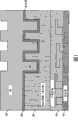
图1为沉积铜之后的部分衬底的截面图。FIG. 1 is a cross-sectional view of a portion of a substrate after copper deposition.
图2为抛光处理之后,部分衬底的截面图。FIG. 2 is a cross-sectional view of a portion of a substrate after a polishing process.
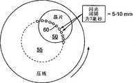
图3示出压板上的衬底。Figure 3 shows a substrate on a platen.
图4示出从部分衬底表面反射的光。Figure 4 shows light reflected from part of the substrate surface.
图5、6及7分别例示铜、电介质材料及阻挡材料的光谱图。Figures 5, 6 and 7 illustrate the spectra of copper, dielectric material and barrier material, respectively.
图8示出与100%铜之光谱相关的关系曲线。Figure 8 shows the correlation curve for the spectrum of 100% copper.
图9示出不同抛光处理阶段的电介质材料光谱。Figure 9 shows the dielectric material spectra at different polishing process stages.
图10示出整个抛光过程中测量光谱与参考光谱的差别,用以判断抛光终点。FIG. 10 shows the difference between the measured spectrum and the reference spectrum during the entire polishing process, which is used to judge the polishing end point.
图11为光谱匹配法的曲线图。Fig. 11 is a graph of the spectral matching method.
图12示出在减去铜之前,整个抛光过程中测量光谱与参考光谱的差别。Figure 12 shows the difference between the measured spectrum and the reference spectrum throughout the polishing process before copper subtraction.
图13及14示出在减去铜之后,整个抛光过程中测量光谱与参考光谱的差别。Figures 13 and 14 show the difference between the measured spectrum and the reference spectrum throughout the polishing process after copper subtraction.
各图中同样的组件符号代表类似的组件。The same reference numerals in the various figures represent similar components.
具体实施方式Detailed ways
具有原位(in-situ)监测模块的抛光系统可用来监测衬底抛光情形,以于作业中(on the fly)或实时(real time)获得抛光资料及判断抛光终点。美国专利申请公开2007-0224915描述此类抛光系统和原位监测模块,其通过引用而结合于此。抛光时,监测模块得到自衬底表面反射的光谱。接着比较该光谱与数据库,藉以判断何时达到终点。The polishing system with an in-situ monitoring module can be used to monitor the polishing situation of the substrate, so as to obtain polishing data and judge the polishing end point during operation (on the fly) or in real time (real time). Such a polishing system and in-situ monitoring module is described in US Patent Application Publication 2007-0224915, which is hereby incorporated by reference. During polishing, the monitoring module obtains the spectrum reflected from the substrate surface. The spectrum is then compared to a database to determine when the endpoint has been reached.
参照图1,其为沉积铜之后部分衬底的截面图,示出硅衬底10上具有下面结构层15、电介质层20、阻挡层25、和铜层30。电介质层20中的凹陷部位35填满铜而构成线路、接垫、和其它传导性特征。如第2图所示,衬底可经一个或多个步骤抛光处理。第一抛光步骤(步骤A)为平坦化铜层30。第二抛光步骤(步骤B)为清除铜线35外部之上阻挡层25上方的铜层30。第三抛光步骤(步骤C)为移除铜线35外部的阻挡层25及移除部分电介质层20。可额外进行抛光步骤。另外,例如可在不同的抛光系统压板上分别进行抛光步骤,或者可在单一压板上合并进行二个或多个步骤。Referring to FIG. 1 , which is a cross-sectional view of a portion of a substrate after copper deposition, a
进行步骤C时,光谱式终点法可用来判断终点。选择期望的电介质层厚度,且在抛光期间,比较实时获得的光谱与抛光光谱数据库内的光谱来判断抛光终点。其潜在的困难点之一在于收集衬底表面的光谱。When carrying out step C, the spectral end point method can be used to judge the end point. The desired thickness of the dielectric layer is selected, and during polishing, the polishing endpoint is determined by comparing the spectra obtained in real time with the spectra in the polished spectral database. One of the potential difficulties is collecting spectra from the substrate surface.
当衬底旋转并移动越过抛光表面时,收集光谱。参照图3,一些抛光系统转动压板上的抛光垫55,而终点侦测系统固接至压板,如此传感器会移动越过衬底50。接着在预定时距及/或间隔内取得衬底50的位置60的光谱,例如约7毫秒(ms)和5-10毫米(mm)。每一光谱为光从测量点(可横跨数毫米)反射的结果。Spectra were collected as the substrate was rotated and moved across the polished surface. Referring to FIG. 3 , some polishing systems rotate a
要精准控制从衬底50的某一位置取得光谱并不容易。如图2所示,除了其它特征外,衬底50尚具有铜线35和电介质层20。铜线35反射的光强度比电介质层20反射的光强度强,且二者光谱分布不同。依据美国专利申请公开2007-0224915所述的终点判断法,可利用电介质区域的光谱来判断终点。然而,铜反射会造成光谱严重失真。任何从铜的反射将扭曲光谱,以致终点判断的原始状态不稳定。It is not easy to precisely control the acquisition of spectra from a certain position on the
参照图4,除了会扭曲光谱外,因无法控制取得与铜线和电介质区域相关的光谱的位置,故铜反射量迥然不同且每次测量结果不一样。此尤其是起因于缺乏精密机动编码器和衬底在承载头上滑动、或是光束扫过衬底的路径未通过每个晶粒的同一位置。一部分光束可照射仅具电介质的区域70,另一部分光束则可从兼具电介质与铜的衬底区域75、80反射(虽然图中只显示从一个铜线反射,但测量点可包括许多线路或其它铜质特征)。包括电介质与铜的区域75、80可含有不同比例的电介质。衬底上各区域的特征密度可彼此不同。尽管某些如内存的集成电路类型包括大范围的规则金属特征,然其它如处理器的集成电路类型呈现不均一的特征分布。因此,即使各区域70、75、80的电介质层厚度相同,呈现的光谱仍将不同。Referring to Figure 4, in addition to distorting the spectrum, since there is no control over where the spectrum is taken relative to the copper wire and dielectric regions, the amount of copper reflection varies widely and varies from measurement to measurement. This arises, inter alia, from the lack of precision motorized encoders and the sliding of the substrate on the carrier head, or from the fact that the path of the beam across the substrate does not pass through the same location on each die. A portion of the beam can illuminate the dielectric only
然而,这些光谱可用来判断抛光终点。光谱可从其取得的原始格式转换成仅显示从无铜区域获得光谱的修改版本。可判定取得原始光谱的区域所含的铜比例,然后减去铜对光谱的贡献影响。However, these spectra can be used to judge the polishing endpoint. Spectra can be converted from the original format in which they were taken to a modified version showing only spectra taken from copper-free regions. It is possible to determine the proportion of copper contained in the region from which the original spectrum was obtained, and then subtract the copper contribution to the spectrum.
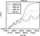
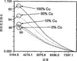
如图5、6及7所示,光谱中铜的反射比预料将增加电介质或氧化物的反射比、或增加阻挡层的反射比(假设已知铜的贡献比例)。参照图5,其显示纯铜层的光谱、纯阻挡层的光谱、以及铜与阻挡层的组合物的光谱。铜反射比在整个波长范围高于阻挡层反射比。在图6中,氧化物亦呈类似现象。铜与氧化物的混合物产生的光谱具有介于二光谱间的反射比值。参照图7,当铜的比例从100%降至50%、10%及0%时,大于5410埃之波长的反射比随之下降。As shown in Figures 5, 6 and 7, the reflectance of copper in the spectrum is expected to increase the reflectance of the dielectric or oxide, or increase the reflectance of the barrier layer (assuming the proportional contribution of copper is known). Referring to Figure 5, there are shown spectra for a pure copper layer, a pure barrier layer, and a combination of copper and barrier layer. The copper reflectance is higher than the barrier reflectance over the entire wavelength range. In Fig. 6, the oxide also exhibits a similar phenomenon. Mixtures of copper and oxides produce spectra with reflectance values intermediate between the two spectra. Referring to FIG. 7, when the proportion of copper is decreased from 100% to 50%, 10% and 0%, the reflectance of wavelengths greater than 5410 angstroms decreases accordingly.
若光谱分别与纯铜或100%铜的光谱相关联,且将结果归一化(normalize);在零迟滞量(zero-lag)下,10%铜的光谱归一化成0.1,50%铜的光谱归一化成0.5。其它比例的铜亦具相似结果。参照图8,其显示在渐增迟滞量(下列方程式的τ)下,与100%铜的光谱相关联的0%、10%、50%、和100%铜的光谱。光谱的起始点92、94、96、98代表各光谱在零迟滞量下的相关性,即比较曲线时,不需沿着x轴位移任一曲线。随着曲线往图右方移动,迟滞量将增加,而相关性将降低。If the spectrum is correlated to that of pure copper or 100% copper, respectively, and the results are normalized; at zero-lag, the spectrum of 10% copper is normalized to 0.1, that of 50% copper Spectra were normalized to 0.5. Other proportions of copper also have similar results. Referring to FIG. 8, which shows the spectra of 0%, 10%, 50%, and 100% copper associated with the spectrum of 100% copper at increasing amounts of hysteresis (τ in the following equation). The starting points 92, 94, 96, 98 of the spectra represent the correlation of each spectrum at zero hysteresis, ie, when comparing the curves, it is not necessary to shift either curve along the x-axis. As the curve moves to the right of the graph, the amount of hysteresis increases and the correlation decreases.
为判定光谱中的铜浓度(即,铜对光谱的贡献比例,此受控于监测表面所含的铜比例),利用以下曲线比较方程式可得到零迟滞量下与纯铜光谱相关的光谱:To determine the copper concentration in the spectrum (i.e., the proportion of copper that contributes to the spectrum, which is controlled by the proportion of copper contained on the surface being monitored), the spectrum relative to the pure copper spectrum at zero hysteresis can be obtained using the following curve comparison equation:
g(λ)为诸如纯铜光谱等曲线之一,h(λ)为测量光谱,dλ表示在所有波长(λ)范围进行积分。g(λ) is one of the curves such as the spectrum of pure copper, h(λ) is the measured spectrum, and dλ represents integration over all wavelength (λ) ranges.
接着,归一化零迟滞量下测量光谱的相关性,以得到介于0至100%间的浓度。此可利用下列方程式达成:Next, the correlation of the spectra measured at zero hysteresis is normalized to obtain concentrations between 0 and 100%. This can be achieved using the following equation:
其中Corr(measured spectrum)为先前计算的Corr(g,h),Corr(non Cu)代表图8的起始点98的值,Corr(pure Cu)代表起始点92的值。常数Corr(non Cu)和Corr(pure Cu)可轻易凭经验判定且适合不同衬底图案。这些常数不需很精准,采用近似值即可使铜减去法大幅改善终点迹线的信杂比。Wherein Corr (measured spectrum) is the previously calculated Corr (g, h), Corr (non Cu) represents the value of the
判定了铜浓度后,减去测量光谱中铜的贡献。假设铜光谱与非铜光谱为线性迭加,且依据面积比例或浓度加权各光谱。减去法可采用以下方程式:Once the copper concentration has been determined, the copper contribution from the measured spectrum is subtracted. A linear superposition of copper and non-copper spectra is assumed, and each spectrum is weighted according to area ratio or concentration. The subtraction method can use the following equation:
M(λ)=(1-fCu)·O(λ)+fCu·C(λ)M(λ)=(1-fCu )·O(λ)+fCu ·C(λ)
其中M(λ)为测量光谱,fCu(从0.0至1.0)为铜的比例,O(λ)为非铜光谱,而C(λ)为铜光谱。解答非铜光谱后可得下列方程式:where M(λ) is the measured spectrum, fCu (from 0.0 to 1.0) is the proportion of copper, O(λ) is the non-copper spectrum, and C(λ) is the copper spectrum. After solving the non-copper spectrum, the following equation can be obtained:
示例example
利用抛光期间自衬底反射之白光光谱来判定抛光终点的方法有两种。第一种方法称为判断终点的差异法。第二种方法在此是指判断终点的光谱指数匹配法。两种方法均进一步说明于美国专利申请公开2007-0224915。There are two methods for determining the endpoint of polishing using the spectrum of white light reflected from the substrate during polishing. The first method is called the difference method of judging the endpoint. The second method refers here to the spectral index matching method for judging the endpoint. Both methods are further described in US Patent Application Publication 2007-0224915.
采行任一方法皆可凭经验或根据理论取得抛光光谱的数据库。参照图9,数据库可包括一个抛光程序的光谱,其始于得自具厚氧化层(厚度在此为8200埃)的衬底的光谱110,且包括贯穿整个抛光程序直到过度抛光衬底(厚度在此为1300埃)的光谱120、130、140、150、160。图中仅显示抛光程序的特定光谱,具体而言为压板转速(Rev.)为1、12、24、36、48、60的光谱。Using either method, a database of polishing spectra can be obtained empirically or theoretically. Referring to FIG. 9, the database may include spectra for a polishing program starting with the
其它层的光谱也可取得并存到数据库,例如阻挡层的光谱。阻挡层光谱可用来判断何时已清除阻挡层。Spectra of other layers can also be obtained and stored in the database, eg spectra of barrier layers. Barrier spectroscopy can be used to tell when the barrier has been removed.
就差异法而言,光谱乃选择对应抛光处理的衬底具有期望终点氧化物厚度。例如,若预定氧化物厚度为2200埃且转速为48,则选择光谱150当作参考光谱。当然也可依需求选择其它终点和参考光谱。For the difference method, the spectrum is selected to correspond to the polished substrate having the desired endpoint oxide thickness. For example, if the predetermined oxide thickness is 2200 Angstroms and the rotational speed is 48,
抛光衬底时将自各层移除不同的材料,例如铜、阻挡材料和氧化物。抛光期间取得的光谱通常反映任一时间的一或多个材料状况。故此方法除了判定氧化物厚度外,还可判断何时已经移除衬底上诸如阻挡层等特定材料。Different materials such as copper, barrier materials and oxides are removed from the various layers when the substrate is polished. Spectra taken during polishing typically reflect one or more material conditions at any one time. Therefore, in addition to determining the oxide thickness, this method can also determine when a specific material on the substrate, such as a barrier layer, has been removed.
比较抛光处理的衬底的光谱与参考光谱150。相比后,二光谱间的差别可以下式表示:The spectrum of the polished substrate is compared to a
其中Rm为测量光谱,Rr为参考光谱。简述之,经平方及加总后可判定出二光谱于各波长的差别。Where Rm is the measured spectrum and Rr is the reference spectrum. Briefly, the difference between the two spectra at each wavelength can be determined after squaring and summing.
参照图10,其绘制平方差的总和与压板转速而产生渐近零的正弦曲线。当差最接近零时,此处称为终点。Referring to Figure 10, which plots the sum of squared differences versus platen rotational speed to produce a sinusoidal curve asymptotically to zero. When the difference is closest to zero, it is called the endpoint here.
另一判定终点的方法为光谱匹配法,包括指定参考光谱的光谱编号。获得抛光时的光谱后,比对光谱与数据库,以判定最匹配测量光谱的光谱编号。匹配数目按时间或压板转速绘制;线与参考光谱编号相交处称为终点。参照图11,其为光谱匹配法的实施例,显示一个符合光谱匹配结果的线。匹配数目按时间绘制。当线与参考光谱编号相交时,即判定于时间点180达到终点。Another method for determining the endpoint is the spectral matching method, which includes specifying the spectral number of the reference spectrum. After obtaining the spectrum during polishing, compare the spectrum with the database to determine the spectrum number that best matches the measured spectrum. The number of matches is plotted against time or platen speed; the point where the line intersects the reference spectrum number is called the end point. Referring to FIG. 11 , it is an embodiment of the spectral matching method, which shows a line conforming to the spectral matching result. The number of matches is plotted against time. The endpoint is determined at
再次参考判断终点的差异法,图10的差值通常无法从原始光谱获得。此乃因为铜的高度反射会随意增添至光谱中。参照图12,使用一般包括氧化物反射与铜反射的原始光谱将产生难以判断终点的图形。图12显示抛光期间的两种不同衬底的差别。需注意图10与图12的差异。图10的正弦曲线很容易辨认,但图12的正弦曲线很难判别。抛光移除阻挡层后,光谱中阻挡层反射的贡献一般为微不足道而可忽略。Referring again to the difference method for judging endpoints, the difference values in Figure 10 are usually not available from the raw spectra. This is because copper's high reflectance adds to the spectrum indiscriminately. Referring to Figure 12, using a raw spectrum that typically includes oxide reflections and copper reflections will produce a graph that is difficult to judge endpoints. Figure 12 shows the difference between two different substrates during polishing. Note the difference between Figure 10 and Figure 12. The sinusoid in Figure 10 is easy to identify, but the sinusoid in Figure 12 is difficult to discern. After polishing to remove the blocking layer, the contribution of the blocking layer reflection in the spectrum is generally insignificant and negligible.
参照图13及14,其示出三种晶片在移除铜的贡献后的差别,其平滑曲线并显示如何判断终点。减去噪声很多的铜曲线210、220、230及利用平顺曲线技术可产生随着时间或压板转速趋近于零的曲线212、222、232。Referring to Figures 13 and 14, which show the difference of the three wafers after removing the copper contribution, smooth the curves and show how to judge the endpoint. Subtracting the much
尽管上述方法是以铜为例,然其亦可应用于其它非电介质材料,例如覆盖诸如阻挡层(例如氮化物)、硅或金属氮化物等下电介质层的金属(例如钨)。Although the above method is exemplified with copper, it can also be applied to other non-dielectric materials, such as metals (eg, tungsten) covering the underlying dielectric layers such as barrier layers (eg, nitrides), silicon or metal nitrides.
虽然铜减去法和终点技术是以判断终点的差异法为例,但此方法同样可应用到所述的光谱匹配法。Although the copper subtraction method and the endpoint technique are exemplified by the difference method for judging the endpoint, this method can also be applied to the spectral matching method described.
抛光处理衬底的抛光工具可包括或可电性连接能进行上述方法来判定抛光终点的处理器。判定抛光终点后,控制器可利用该终点发出信号通知抛光工具停止抛光。A polishing tool for polishing a substrate may include or be electrically connected to a processor capable of performing the method described above to determine polishing endpoint. After determining the polishing end point, the controller can use the end point to send a signal to notify the polishing tool to stop polishing.
本发明的实施例和说明书所述的所有功能运作的实施例可采用数字电子电路、或计算机软件、韧体或硬件,包括本说明书提及的结构装置和其结构均等物、或其组合物。本发明的实施例可实施到一个或多个计算机程序产品,即一个或多个实体收录于信息载体(如机器可读取的储存装置或传播信号)的计算机程序,用以执行或控制数据处理设备的运作,例如可程序化处理器、计算机、或多元处理器或计算机。计算机程序(亦已知为程序、软件、软件应用、或编码)可以任一包括编译或解译语言的程序语言编写,其并可配置成任一型式,包括独立程序或模块、组件、子程序、或其它适合计算环境的单元。计算机程序不一定要对应于档案。程序可储存在含有其它程序或资料的档案、提问程序专用的档案、或多重坐标档案(例如储存一或多个模块、子程序或部分编码的档案)。计算机程序可配置供单一计算机或多个位于网点或遍及多个网点且由通信网络相连的计算机执行。Embodiments of the present invention and embodiments of all functional operations described in the description may use digital electronic circuits, or computer software, firmware or hardware, including the structural devices mentioned in this description and their structural equivalents, or combinations thereof. Embodiments of the present invention may be implemented in one or more computer program products, that is, one or more computer programs embodied in an information carrier (such as a machine-readable storage device or a propagated signal) for performing or controlling data processing The operation of a device, such as a programmable processor, computer, or multiple processors or computers. A computer program (also known as a program, software, software application, or code) can be written in any programming language, including compiled or interpreted languages, and can be configured in any form, including stand-alone programs or modules, components, subroutines , or other units suitable for the computing environment. A computer program does not necessarily correspond to a file. A program may be stored in a file containing other programs or data, in a file dedicated to interrogation programs, or in a multi-coordinate file (eg, a file storing one or more modules, subroutines, or portions of code). A computer program can be deployed to be executed by a single computer or by multiple computers that are located at one site or spread across multiple sites and connected by a communication network.
一个或多个执行一个或多个计算机程序的可程序化处理器可藉由运算输入资料及产生输出而进行说明书所述的处理和逻辑流程。诸如现场可程序化门阵列(field programmable gate array;FPGA)或特定功能集成电路(application specific integrated circuit;ASIC)等具特殊用途的逻辑电路也可用来进行处理和逻辑流程。One or more programmable processors executing one or more computer programs can perform the processes and logic flows described in the specification by operating on input data and generating output. Special purpose logic circuits such as field programmable gate arrays (FPGAs) or application specific integrated circuits (ASICs) may also be used for processing and logic flow.
上述抛光设备和方法可应用到各种抛光系统。抛光垫或承载头、或二者可于抛光表面与衬底之间相对移动。例如,压板可绕行而非旋转。抛光垫可为固接压板的圆形垫(或具其它形状)。终点侦测系统的某些态样可应用于线性抛光系统,例如抛光垫为连续式或线性移动的盘式带状抛光垫。抛光层可为标准抛光材料(例如含或不含填料之聚胺甲酸酯)、软性材料、或固定抛光材料。在此描述相对位置关系;应理解抛光表面与衬底可呈垂直或其它方位。虽然在此为叙述减去光谱中铜的贡献,但也可以类似方式移去衬底上诸如阻挡材料等其它元素的反射。故其它实施例亦不脱离后附权利要求书所界定之保护范围。The polishing apparatus and method described above can be applied to various polishing systems. The polishing pad or the carrier head, or both, are relatively movable between the polishing surface and the substrate. For example, the platen may orbit rather than rotate. The polishing pad can be a circular pad (or have other shapes) fixed to the platen. Some aspects of the endpoint detection system can be applied to a linear polishing system, such as a continuous or linearly moving disk-like polishing pad. The polishing layer can be a standard polishing material such as polyurethane with or without fillers, a soft material, or a fixed polishing material. The relative positional relationship is described here; it is understood that the polishing surface and substrate may be perpendicular or in other orientations. While subtracting the contribution of copper from the spectrum is described here, reflections from other elements on the substrate, such as barrier materials, can also be removed in a similar manner. Therefore, other embodiments do not depart from the scope of protection defined by the appended claims.
Claims (20)
Translated fromChineseApplications Claiming Priority (5)
| Application Number | Priority Date | Filing Date | Title |
|---|---|---|---|
| US86867306P | 2006-12-05 | 2006-12-05 | |
| US60/868,673 | 2006-12-05 | ||
| US11/868,911US7768659B2 (en) | 2006-12-05 | 2007-10-08 | Determining copper concentration in spectra |
| US11/868,911 | 2007-10-08 | ||
| PCT/US2007/086535WO2008070736A1 (en) | 2006-12-05 | 2007-12-05 | Determining copper concentration in spectra |
Publications (2)
| Publication Number | Publication Date |
|---|---|
| CN101432616Atrue CN101432616A (en) | 2009-05-13 |
| CN101432616B CN101432616B (en) | 2011-08-17 |
Family
ID=39323797
Family Applications (1)
| Application Number | Title | Priority Date | Filing Date |
|---|---|---|---|
| CN2007800147413AExpired - Fee RelatedCN101432616B (en) | 2006-12-05 | 2007-12-05 | Method for Determining Copper Concentration in Spectrum |
Country Status (4)
| Country | Link |
|---|---|
| US (1) | US7768659B2 (en) |
| CN (1) | CN101432616B (en) |
| TW (1) | TWI382484B (en) |
| WO (1) | WO2008070736A1 (en) |
Cited By (1)
| Publication number | Priority date | Publication date | Assignee | Title |
|---|---|---|---|---|
| CN103155110A (en)* | 2010-08-06 | 2013-06-12 | 应用材料公司 | Techniques for matching measured spectra to reference spectra for in-situ optical monitoring |
Families Citing this family (8)
| Publication number | Priority date | Publication date | Assignee | Title |
|---|---|---|---|---|
| JP5774482B2 (en)* | 2008-10-27 | 2015-09-09 | アプライド マテリアルズ インコーポレイテッドApplied Materials,Incorporated | Goodness of fit in spectral monitoring of substrates during processing |
| US20100114532A1 (en)* | 2008-11-03 | 2010-05-06 | Applied Materials, Inc. | Weighted spectrographic monitoring of a substrate during processing |
| JP5728239B2 (en)* | 2010-03-02 | 2015-06-03 | 株式会社荏原製作所 | Polishing monitoring method, polishing method, polishing monitoring apparatus, and polishing apparatus |
| US8954186B2 (en) | 2010-07-30 | 2015-02-10 | Applied Materials, Inc. | Selecting reference libraries for monitoring of multiple zones on a substrate |
| US8892568B2 (en)* | 2010-10-15 | 2014-11-18 | Applied Materials, Inc. | Building a library of spectra for optical monitoring |
| US8942842B2 (en) | 2011-04-28 | 2015-01-27 | Applied Materials, Inc. | Varying optical coefficients to generate spectra for polishing control |
| US9168630B2 (en)* | 2012-04-23 | 2015-10-27 | Applied Materials, Inc. | User-input functions for data sequences in polishing endpoint detection |
| US20140242881A1 (en)* | 2013-02-27 | 2014-08-28 | Applied Materials, Inc. | Feed forward parameter values for use in theoretically generating spectra |
Family Cites Families (12)
| Publication number | Priority date | Publication date | Assignee | Title |
|---|---|---|---|---|
| JPH11325840A (en)* | 1998-05-19 | 1999-11-26 | Dainippon Screen Mfg Co Ltd | Method and apparatus for judging whether or not remaining metal film exists |
| US6271047B1 (en)* | 1998-05-21 | 2001-08-07 | Nikon Corporation | Layer-thickness detection methods and apparatus for wafers and the like, and polishing apparatus comprising same |
| AU763570B2 (en)* | 1998-08-14 | 2003-07-24 | Spectro Scientific, Inc. | On-site analyzer |
| TW398036B (en)* | 1998-08-18 | 2000-07-11 | Promos Technologies Inc | Method of monitoring of chemical mechanical polishing end point and uniformity |
| US7095511B2 (en)* | 2000-07-06 | 2006-08-22 | Filmetrics, Inc. | Method and apparatus for high-speed thickness mapping of patterned thin films |
| US6664557B1 (en)* | 2001-03-19 | 2003-12-16 | Lam Research Corporation | In-situ detection of thin-metal interface using optical interference |
| US6747283B1 (en)* | 2001-03-19 | 2004-06-08 | Lam Research Corporation | In-situ detection of thin-metal interface using high resolution spectral analysis of optical interference |
| US6821794B2 (en)* | 2001-10-04 | 2004-11-23 | Novellus Systems, Inc. | Flexible snapshot in endpoint detection |
| JP3645226B2 (en) | 2002-03-11 | 2005-05-11 | 株式会社半導体先端テクノロジーズ | Polishing method and polishing residue detection method |
| JP3779636B2 (en)* | 2002-03-27 | 2006-05-31 | 株式会社東芝 | Determination method of residual film by optical measurement |
| CN1492213A (en)* | 2002-10-23 | 2004-04-28 | 台湾积体电路制造股份有限公司 | Method for measuring thickness of non-metal layer in chemical mechanical polishing process |
| US20050026542A1 (en)* | 2003-07-31 | 2005-02-03 | Tezer Battal | Detection system for chemical-mechanical planarization tool |
- 2007
- 2007-10-08USUS11/868,911patent/US7768659B2/ennot_activeExpired - Fee Related
- 2007-11-23TWTW096144632Apatent/TWI382484B/ennot_activeIP Right Cessation
- 2007-12-05CNCN2007800147413Apatent/CN101432616B/ennot_activeExpired - Fee Related
- 2007-12-05WOPCT/US2007/086535patent/WO2008070736A1/enactiveApplication Filing
Cited By (1)
| Publication number | Priority date | Publication date | Assignee | Title |
|---|---|---|---|---|
| CN103155110A (en)* | 2010-08-06 | 2013-06-12 | 应用材料公司 | Techniques for matching measured spectra to reference spectra for in-situ optical monitoring |
Also Published As
| Publication number | Publication date |
|---|---|
| WO2008070736A8 (en) | 2008-08-07 |
| US7768659B2 (en) | 2010-08-03 |
| WO2008070736A1 (en) | 2008-06-12 |
| TWI382484B (en) | 2013-01-11 |
| CN101432616B (en) | 2011-08-17 |
| TW200832585A (en) | 2008-08-01 |
| US20080130000A1 (en) | 2008-06-05 |
Similar Documents
| Publication | Publication Date | Title |
|---|---|---|
| CN101432616A (en) | Method for Determining Copper Concentration in Spectrum | |
| US8747189B2 (en) | Method of controlling polishing | |
| KR100971836B1 (en) | Broadband Optical Endpoint Detection System and Method for Film Change Instruction | |
| US8892568B2 (en) | Building a library of spectra for optical monitoring | |
| JP5542802B2 (en) | Endpoint detection in chemical mechanical polishing using multiple spectra | |
| US6489624B1 (en) | Apparatus and methods for detecting thickness of a patterned layer | |
| US8860932B2 (en) | Detection of layer clearing using spectral monitoring | |
| US8944884B2 (en) | Fitting of optical model to measured spectrum | |
| US20120278028A1 (en) | Generating model based spectra library for polishing | |
| US8942842B2 (en) | Varying optical coefficients to generate spectra for polishing control | |
| JP3327175B2 (en) | Detection unit and wafer polishing apparatus provided with the detection unit | |
| JPH0851090A (en) | Method of grinding patterned layer on semiconductor substrate | |
| US9011202B2 (en) | Fitting of optical model with diffraction effects to measured spectrum | |
| US6464563B1 (en) | Method and apparatus for detecting dishing in a polished layer | |
| US20100103422A1 (en) | Goodness of fit in spectrographic monitoring of a substrate during processing | |
| US8657646B2 (en) | Endpoint detection using spectrum feature trajectories | |
| KR20140028028A (en) | Varying coefficients and functions for polishing control | |
| US6524163B1 (en) | Method and apparatus for controlling a polishing process based on scatterometry derived film thickness variation | |
| US6885446B2 (en) | Method and system for monitoring a process of material removal from the surface of a patterned structure | |
| US6451700B1 (en) | Method and apparatus for measuring planarity of a polished layer | |
| WO2001060242A2 (en) | Test structure for metal cmp process control | |
| JP4427767B2 (en) | Measuring method | |
| Chan et al. | Process control and monitoring with laser interferometry based endpoint detection in chemical mechanical planarization | |
| US6980300B1 (en) | Method and apparatus for generating a polishing process endpoint signal using scatterometry | |
| JP2006032764A (en) | Polishing control method, polishing apparatus, and semiconductor device manufacturing method |
Legal Events
| Date | Code | Title | Description |
|---|---|---|---|
| C06 | Publication | ||
| PB01 | Publication | ||
| C10 | Entry into substantive examination | ||
| SE01 | Entry into force of request for substantive examination | ||
| C14 | Grant of patent or utility model | ||
| GR01 | Patent grant | ||
| CF01 | Termination of patent right due to non-payment of annual fee | Granted publication date:20110817 Termination date:20151205 | |
| EXPY | Termination of patent right or utility model |