CN101427182B - Composite patterning equipment for soft lithography - Google Patents
Composite patterning equipment for soft lithographyDownload PDFInfo
- Publication number
- CN101427182B CN101427182BCN2005800135741ACN200580013574ACN101427182BCN 101427182 BCN101427182 BCN 101427182BCN 2005800135741 ACN2005800135741 ACN 2005800135741ACN 200580013574 ACN200580013574 ACN 200580013574ACN 101427182 BCN101427182 BCN 101427182B
- Authority
- CN
- China
- Prior art keywords
- layer
- polymer layer
- contact
- modulus
- equipment
- Prior art date
- Legal status (The legal status is an assumption and is not a legal conclusion. Google has not performed a legal analysis and makes no representation as to the accuracy of the status listed.)
- Expired - Lifetime
Links
Images


Classifications
- C—CHEMISTRY; METALLURGY
- C04—CEMENTS; CONCRETE; ARTIFICIAL STONE; CERAMICS; REFRACTORIES
- C04B—LIME, MAGNESIA; SLAG; CEMENTS; COMPOSITIONS THEREOF, e.g. MORTARS, CONCRETE OR LIKE BUILDING MATERIALS; ARTIFICIAL STONE; CERAMICS; REFRACTORIES; TREATMENT OF NATURAL STONE
- C04B24/00—Use of organic materials as active ingredients for mortars, concrete or artificial stone, e.g. plasticisers
- C04B24/24—Macromolecular compounds
- C04B24/38—Polysaccharides or derivatives thereof
- C04B24/383—Cellulose or derivatives thereof
- B—PERFORMING OPERATIONS; TRANSPORTING
- B81—MICROSTRUCTURAL TECHNOLOGY
- B81C—PROCESSES OR APPARATUS SPECIALLY ADAPTED FOR THE MANUFACTURE OR TREATMENT OF MICROSTRUCTURAL DEVICES OR SYSTEMS
- B81C1/00—Manufacture or treatment of devices or systems in or on a substrate
- B81C1/00436—Shaping materials, i.e. techniques for structuring the substrate or the layers on the substrate
- B81C1/00444—Surface micromachining, i.e. structuring layers on the substrate
- B81C1/0046—Surface micromachining, i.e. structuring layers on the substrate using stamping, e.g. imprinting
- B—PERFORMING OPERATIONS; TRANSPORTING
- B82—NANOTECHNOLOGY
- B82Y—SPECIFIC USES OR APPLICATIONS OF NANOSTRUCTURES; MEASUREMENT OR ANALYSIS OF NANOSTRUCTURES; MANUFACTURE OR TREATMENT OF NANOSTRUCTURES
- B82Y10/00—Nanotechnology for information processing, storage or transmission, e.g. quantum computing or single electron logic
- B—PERFORMING OPERATIONS; TRANSPORTING
- B82—NANOTECHNOLOGY
- B82Y—SPECIFIC USES OR APPLICATIONS OF NANOSTRUCTURES; MEASUREMENT OR ANALYSIS OF NANOSTRUCTURES; MANUFACTURE OR TREATMENT OF NANOSTRUCTURES
- B82Y30/00—Nanotechnology for materials or surface science, e.g. nanocomposites
- B—PERFORMING OPERATIONS; TRANSPORTING
- B82—NANOTECHNOLOGY
- B82Y—SPECIFIC USES OR APPLICATIONS OF NANOSTRUCTURES; MEASUREMENT OR ANALYSIS OF NANOSTRUCTURES; MANUFACTURE OR TREATMENT OF NANOSTRUCTURES
- B82Y40/00—Manufacture or treatment of nanostructures
- C—CHEMISTRY; METALLURGY
- C04—CEMENTS; CONCRETE; ARTIFICIAL STONE; CERAMICS; REFRACTORIES
- C04B—LIME, MAGNESIA; SLAG; CEMENTS; COMPOSITIONS THEREOF, e.g. MORTARS, CONCRETE OR LIKE BUILDING MATERIALS; ARTIFICIAL STONE; CERAMICS; REFRACTORIES; TREATMENT OF NATURAL STONE
- C04B28/00—Compositions of mortars, concrete or artificial stone, containing inorganic binders or the reaction product of an inorganic and an organic binder, e.g. polycarboxylate cements
- C04B28/14—Compositions of mortars, concrete or artificial stone, containing inorganic binders or the reaction product of an inorganic and an organic binder, e.g. polycarboxylate cements containing calcium sulfate cements
- G—PHYSICS
- G03—PHOTOGRAPHY; CINEMATOGRAPHY; ANALOGOUS TECHNIQUES USING WAVES OTHER THAN OPTICAL WAVES; ELECTROGRAPHY; HOLOGRAPHY
- G03F—PHOTOMECHANICAL PRODUCTION OF TEXTURED OR PATTERNED SURFACES, e.g. FOR PRINTING, FOR PROCESSING OF SEMICONDUCTOR DEVICES; MATERIALS THEREFOR; ORIGINALS THEREFOR; APPARATUS SPECIALLY ADAPTED THEREFOR
- G03F7/00—Photomechanical, e.g. photolithographic, production of textured or patterned surfaces, e.g. printing surfaces; Materials therefor, e.g. comprising photoresists; Apparatus specially adapted therefor
- G03F7/0002—Lithographic processes using patterning methods other than those involving the exposure to radiation, e.g. by stamping
- C—CHEMISTRY; METALLURGY
- C04—CEMENTS; CONCRETE; ARTIFICIAL STONE; CERAMICS; REFRACTORIES
- C04B—LIME, MAGNESIA; SLAG; CEMENTS; COMPOSITIONS THEREOF, e.g. MORTARS, CONCRETE OR LIKE BUILDING MATERIALS; ARTIFICIAL STONE; CERAMICS; REFRACTORIES; TREATMENT OF NATURAL STONE
- C04B2111/00—Mortars, concrete or artificial stone or mixtures to prepare them, characterised by specific function, property or use
- C04B2111/00034—Physico-chemical characteristics of the mixtures
- C04B2111/00181—Mixtures specially adapted for three-dimensional printing (3DP), stereo-lithography or prototyping
Landscapes
- Chemical & Material Sciences (AREA)
- Engineering & Computer Science (AREA)
- Nanotechnology (AREA)
- Ceramic Engineering (AREA)
- Physics & Mathematics (AREA)
- Crystallography & Structural Chemistry (AREA)
- Materials Engineering (AREA)
- General Physics & Mathematics (AREA)
- Structural Engineering (AREA)
- Organic Chemistry (AREA)
- Condensed Matter Physics & Semiconductors (AREA)
- Manufacturing & Machinery (AREA)
- Mathematical Physics (AREA)
- Theoretical Computer Science (AREA)
- Inorganic Chemistry (AREA)
- Chemical Kinetics & Catalysis (AREA)
- Microelectronics & Electronic Packaging (AREA)
- Composite Materials (AREA)
- Shaping Of Tube Ends By Bending Or Straightening (AREA)
- Laminated Bodies (AREA)
- Exposure Of Semiconductors, Excluding Electron Or Ion Beam Exposure (AREA)
Abstract
Description
Translated fromChinese对相关申请的交叉引用 Cross References to Related Applications
本申请要求于2004年4月27日提交的美国临时专利申请60/565,604的优先权,在此通过引用,将其全部内容以不与本申请所公开内容矛盾的程度纳入本说明书。 This application claims priority to US
背景技术Background technique
微米级结构和器件的设计与制造已对多项重要技术—包括微电子学、光电子学、微流体技术和微传感技术—构成巨大影响。例如,制造微米级(microsized)电子器件的能力已经使电子学领域发生巨大变化,获得了性能更快更高、能量需求显著降低的电子元件。随着这些技术的不断快速发展而日益明显的是,通过开发在纳米级上操纵和组织物质的能力,将得到更多的益处。纳米科技的进步将可望对从材料科学到应用工程到生物技术的许多技术领域产生显著影响。The design and fabrication of micron-scale structures and devices has had a huge impact on several important technologies, including microelectronics, optoelectronics, microfluidics, and microsensing. For example, the ability to manufacture microsized electronic devices has revolutionized the field of electronics, enabling faster and higher performance electronic components with significantly lower energy requirements. As these technologies continue to advance at a rapid pace, it becomes increasingly apparent that further benefits will be gained by developing the ability to manipulate and organize matter at the nanoscale. Advances in nanotechnology are expected to have a significant impact on many technical fields, from materials science to applied engineering to biotechnology.
具有纳米级尺寸的器件的制造不仅仅是微型化概念的自然延伸,它还是一个在物理和化学行为上区别于较大型体系的根本不同的领域。例如,很多材料的纳米级组装行为显著受其大的界面体积分数以及电子束缚引起的量子机械效应的影响。制造具有边界清晰的、纳米级零部件(features)的结构的能力,已经使制造基于其性能和过程仅发生于纳米尺寸上的器件成为可能,所述性能和过程包括例如单电子隧道效应、库伦堵塞和量子尺寸效应。然而,由各种材料制造亚微米级结构的商业化实用方法的开发,对纳米科技的不断发展而言是关键所在。The fabrication of devices with nanoscale dimensions is not just a natural extension of the concept of miniaturization, it is a fundamentally different field that differs in physical and chemical behavior from larger systems. For example, the nanoscale assembly behavior of many materials is significantly affected by their large interfacial volume fractions and quantum mechanical effects caused by electron confinement. The ability to fabricate structures with well-defined, nanoscale features has enabled the fabrication of devices based on properties and processes that occur only at the nanoscale, including, for example, single-electron tunneling, Coulombic Blockage and quantum size effects. However, the development of commercially practical methods for fabricating submicron-scale structures from a variety of materials is critical to the continued advancement of nanotechnology.
光刻法(photolithography)是目前最普遍使用的微制造方法,几乎所有的集成电路都是用这种技术制造的。在常规的投影模式(projection mode)光刻法中,用光掩模生成一个与选定的二维图案对应的光学图像。将该图像进行光学还原(optically reduce)并投射到旋涂于基片上的光致抗蚀剂薄膜上。或者,在直接写至晶片(DirectWrite to Wafer)光刻技术中,将光致抗蚀剂直接暴露于激光、电子束或离子束,而不使用光掩模。光、电子和/或离子与光致抗蚀剂所含分子 之间的相互作用使选定的光致抗蚀剂区域发生化学变化,变化的方式使得能够制造具有清晰的物理尺寸的结构。光刻法非常适于在平面上生成二维分布零部件。此外,采用涉及形成多叠层的叠加制造方法,光刻法能够在平面上生成更复杂的三维分布零部件。Photolithography (photolithography) is currently the most commonly used microfabrication method, and almost all integrated circuits are manufactured using this technology. In conventional projection mode lithography, a photomask is used to generate an optical image corresponding to a selected two-dimensional pattern. The image was optically reduced and projected onto a photoresist film spun onto a substrate. Alternatively, in Direct Write to Wafer lithography, the photoresist is directly exposed to a laser, electron beam, or ion beam without the use of a photomask. The interaction of light, electrons, and/or ions with the molecules contained in the photoresist chemically changes selected photoresist regions in such a way that structures with well-defined physical dimensions can be fabricated. Photolithography is well suited for producing two-dimensionally distributed components on a plane. In addition, photolithography enables the generation of more complex three-dimensionally distributed components on a plane, using additive manufacturing methods that involve the formation of multiple stacked layers.
光刻法的新发展已经使其应用扩展到具有亚微米级尺寸的结构的制造中。例如,纳米光刻技术,如UV深投影模式光刻法、软X射线光刻法、电子束光刻法和扫描探针法已经成功地用于制造具有10至100纳米级零部件的结构。虽然纳米光刻法提供了制造具有纳米尺寸的结构和器件的可行方法,但是这些方法具有某些限制,这阻止了其与低成本、高产量的纳米材料商业化加工方法的有效结合。首先,纳米光刻法需要精细且昂贵的分档器或写工具(write tool),以将光、电子和/或离子导向光致抗蚀剂表面上。第二,这些方法限于对很窄范围内的专用材料进行构图,并且不太适于在纳米结构中引入特定的化学官能团。第三,常规的纳米光刻法限于在无机基片的小面积超平刚性表面上制造纳米级零部件,因而不太适于在玻璃、碳和塑料表面上构图。最后,由于纳米光刻法提供的焦距深度受限,并且通常需要繁重的多层重复加工,因此难以制造包含其零部件具有三维可选长度的纳米结构。New developments in photolithography have extended their application to the fabrication of structures with submicron-scale dimensions. For example, nanolithography techniques such as UV deep projection mode lithography, soft X-ray lithography, electron beam lithography, and scanning probe methods have been successfully used to fabricate structures with features on the scale of 10 to 100 nanometers. Although nanolithography offers viable methods for fabricating structures and devices with nanometer dimensions, these methods have certain limitations that prevent their effective integration with low-cost, high-throughput commercial processing methods for nanomaterials. First, nanolithography requires elaborate and expensive steppers or write tools to direct light, electrons and/or ions onto the photoresist surface. Second, these methods are limited to patterning a narrow range of specialized materials and are not well suited for introducing specific chemical functional groups into nanostructures. Third, conventional nanolithography is limited to fabricating nanoscale features on small, ultraflat, rigid surfaces of inorganic substrates, making them less suitable for patterning on glass, carbon, and plastic surfaces. Finally, fabrication of nanostructures containing components with three-dimensionally selectable lengths is difficult due to the limited depth of focus offered by nanolithography and the often heavy, multi-layer reprocessing required.
光刻法用于纳米制造的实用性限制,激发了对开发制造纳米级结构的替代的、非光刻的方法的强烈兴趣。近些年,已经开发了基于模塑(molding)、接触印刷和压印(embossing)的、统称为软光刻法(softlithography)的新技术。这些技术使用可适应的(conformable)构图设备,例如印模、塑模或掩模,这些设备具有包含清晰的凸起图案(reliefpattern)的转印面(transfer surface)。通过材料处理过程—该过程包括基片和构图设备转印面之间的分子级的共形接触(conformalcontact)——形成微米级和纳米级(nonosized)的结构。用于软光刻法中的构图设备通常包括弹性体材料,例如聚(二甲基硅氧烷)(PDMS),并且通常通过将预聚物浇铸于用常规光刻法形成的母板上而制备。构图设备的机械特性对于制造具有良好的保真度和定位精度的、高机械强度的被转印材料图案而言非常重要。The practical limitations of photolithography for nanofabrication have spurred intense interest in developing alternative, non-lithographic methods for fabricating nanoscale structures. In recent years, new technologies based on molding, contact printing and embossing, collectively called softlithography, have been developed. These techniques use conformable patterning devices, such as stamps, molds or masks, which have a transfer surface containing a defined relief pattern. Microscale and nanoscale (nonsized) structures are formed through material handling processes that include molecular-scale conformal contact between the substrate and the transfer surface of the patterning device. Patterning devices used in soft lithography typically comprise elastomeric materials such as poly(dimethylsiloxane) (PDMS), and are typically fabricated by casting a prepolymer onto a master formed by conventional lithography. preparation. The mechanical properties of the patterning device are very important for producing mechanically robust patterns of the transferred material with good fidelity and positioning accuracy.
能够生成微米级和/或纳米级结构的软光刻方法包括纳米转印(nanotransfer printing)、微转印模塑(microtransfer molding)、 再模塑(replica molding)、毛细管微模塑(micromolding incapillaries)、近场移相光刻(near field phase shift lithography)以及溶剂辅助微模塑(solvent assisted micromolding)。例如,常规的软光刻接触印刷方法已用于生成金的自组装单层图案,该图案具有侧向尺寸小至约250nm的零部件。软光刻法生成的结构已被结合到各种器件中,包括二极管、荧光多孔硅烷像素、有机发光二极管和薄膜晶体管中。该技术的其它应用通常包括制造柔性电子元件、微机电系统、微分析系统以及纳米光子系统(nanophotonic system)。Soft lithography methods capable of generating microscale and/or nanoscale structures include nanotransfer printing, microtransfer molding, replica molding, micromolding incapillaries , near field phase shift lithography (near field phase shift lithography) and solvent assisted micromolding (solvent assisted micromolding). For example, conventional soft-lithographic contact printing methods have been used to generate self-assembled monolayer patterns of gold with features as small as about 250 nm in lateral dimension. Soft lithography-generated structures have been incorporated into a variety of devices, including diodes, fluorescent porous silane pixels, organic light-emitting diodes, and thin-film transistors. Other applications of this technology generally include the fabrication of flexible electronic components, microelectromechanical systems, microanalytical systems, and nanophotonic systems.
制造纳米结构的软光刻方法提供了对于制造纳米级结构和器件而言重要的许多优点。首先,这些方法适用于范围广泛的基片,例如柔性塑料、含碳材料、陶瓷、硅和玻璃,并且适用于范围广泛的转印材料,包括金属、有机复合物、胶体材料、悬浮体、生物分子、细胞和盐溶液。第二,软光刻法既能够在平面上、也能够在曲面上生成被转印材料的零部件,并且能够快速有效地在基片的大面积上构图。第三,软光刻技术很适合具有下述特征的三维结构的纳米制造:所述三维结构的零部件在三维上具有可选择性调整的长度。最后,软光刻法提供了低成本的方法,该方法可望适合于现有的商业化印刷和模塑技术。Soft lithographic methods of fabricating nanostructures offer many advantages that are important for fabricating nanoscale structures and devices. First, these methods are applicable to a wide range of substrates, such as flexible plastics, carbonaceous materials, ceramics, silicon, and glass, and to a wide range of transfer materials, including metals, organic composites, colloidal materials, suspensions, biological Molecules, cells and salt solutions. Second, soft lithography is capable of generating features of transferred material on both flat and curved surfaces, and can pattern large areas of substrates quickly and efficiently. Third, soft lithography is well suited for the nanofabrication of three-dimensional structures whose features have selectively adjustable lengths in three dimensions. Finally, soft lithography offers low-cost methods that are expected to be amenable to existing commercial printing and molding techniques.
虽然常规的PDMS构图设备能够与多种基片材料和表面形态(surface contours)形成可复制的共形接触,但是用这些设备制造小于100nm范围内的零部件时会遇到与压力引起的变形相关的问题,因为常规的单层PDMS印模和塑模具有低模量(3MPa)和高压缩率(2.0N/mm2)。首先,在长宽比小于约0.3时,具有宽且浅的凸起零部件的常规PDMS构图设备在与基片表面接触时易于塌陷(collapse)。第二,具有间距小的(<约200nm)、窄的(<约200nm)结构的常规单层PDMS构图设备的相邻零部件在与基片表面接触时易于一起塌陷。最后,当常规的PDMS印模从基片上剥离时,由于表面张力,印模易于使被转印图案中的尖锐转角变圆。这些问题的综合效果是给被转印到基片上的材料图案带来不期望的变形。为使常规的单层PDMS构图设备引起的图案变形最小化,已经将包含多层印模和塑模的复合构图设备作为生成尺寸小于100nm的结构的装置进行了检验。While conventional PDMS patterning equipment is capable of forming reproducible conformal contacts with a wide variety of substrate materials and surface contours, fabrication of parts in the sub-100nm range with these equipment suffers from pressure-induced deformations problem because conventional monolayer PDMS stamps and molds have low modulus (3 MPa) and high compressibility (2.0 N/mm2 ). First, at aspect ratios less than about 0.3, conventional PDMS patterning devices with wide and shallow raised features tend to collapse when in contact with the substrate surface. Second, adjacent features of conventional single-layer PDMS patterning devices with closely spaced (<about 200 nm), narrow (<about 200 nm) structures tend to collapse together when in contact with the substrate surface. Finally, when a conventional PDMS stamp is peeled from the substrate, the stamp tends to round the sharp corners in the transferred pattern due to surface tension. The combined effect of these problems is to introduce undesirable distortions in the pattern of material being transferred to the substrate. To minimize pattern distortion induced by conventional single-layer PDMS patterning devices, composite patterning devices comprising multilayer stamps and molds have been examined as means to generate structures with dimensions smaller than 100 nm.
Michel及其合作者报道了使用复合印模的微接触印刷方法,所述复 合印模由结合于弹性体层上的可弯曲的金属、玻璃或聚合物薄层组成,所述弹性体层上具有带有凸起图案的转印面。[Michel等,PrintingMeets Lithography:Soft Approaches to High Resolution Patterning,IBM J.Res.& Dev.,第45卷,第5期,第697-719页(2001年9月)。这些作者还描述了一种复合印模设计,该印模由刚性的支撑层和聚合物背衬层组成,所述聚合物背衬层包括软的第一聚合物层及与其相连的较硬的第二层,该第二层具有带有凸起图案的转印面。据这些作者报道,所公开的复合印模设计可用于“大面积、高分辨率印刷应用,其零部件尺寸小至80nm”。Michel and co-workers reported a microcontact printing method using a composite stamp consisting of a thin flexible metal, glass, or polymer layer bonded to an elastomeric layer on which Features a transfer side with a raised pattern. [Michel et al., Printing Meets Lithography: Soft Approaches to High Resolution Patterning, IBM J. Res. & Dev., Vol. 45, No. 5, pp. 697-719 (September 2001). These authors also describe a composite impression design consisting of a rigid support layer and a polymer backing layer consisting of a soft first polymer layer attached to a stiffer A second layer having a transfer surface with a raised pattern. According to the authors, the disclosed composite stamp design can be used for "large-area, high-resolution printing applications with feature sizes as small as 80nm."
Odom及其合作者公开了一种复合的两层印模设计,该印模由厚的(≈3mm)184PDMS背衬层及与其相连的薄的(30-40微米)h-PDMS层所组成,该h-PDMS层具有带有凸起图案的转印面。[Odem等,Langmuir,第18卷,第5314-5320页(2002)。在该研究中,该复合印模用于在软光刻移相光刻方法模塑形成具有100nm量级的尺寸的零部件。据这些作者报道,所公开的复合印模具有提高的机械稳定性,这使得与常规的低模量单层PDMS印模相比,侧壁的膨胀和下垂的情况减少。Odom and co-workers disclosed a composite two-layer stamp design consisting of a thick (≈3mm) 184PDMS backing layer connected to it by a thin (30-40μm) h-PDMS layer, The h-PDMS layer has a transfer surface with a raised pattern. [Odem et al., Langmuir, Vol. 18, pp. 5314-5320 (2002). In this study, the composite stamp was used to mold features with dimensions on the order of 100 nm in soft lithography phase-shift lithography. According to these authors, the disclosed composite impressions have improved mechanical stability, which results in less swelling and sagging of the sidewalls compared to conventional low modulus monolayer PDMS impressions.
虽然使用常规的复合印模和塑模,已经在某种程度上提高了软光刻方法生成尺寸在小于100nm范围内的零部件的能力,但是这些技术仍然易于发生很多问题,这阻碍了其在高产量微米级和纳米级器件制造中的有效商业化应用。首先,一些常规的复合印模和塑模设计具有有限的柔性,因而不能与曲面或粗糙面形成良好的共形接触。第二,常规的多材料PDMS印模的凸起图案易于在热固化或紫外固化过程中发生不想要的收缩,这使凸起图案在其转印面上发生变形。第三,使用含有多层、且各层具有不同的热膨胀系数的常规复合印模,可以导致因温度变化引起的凸起图案变形及其转印面的弯曲。第四,使用硬的和/或脆的背衬层,例如玻璃和某些金属层,使得难以将常规的复合印模结合到现有的商品化印刷机配置——例如辊筒印刷和柔版印刷配置——中。最后,使用具有转印面、且该转印面包括高模量弹性体材料的复合印模,妨碍了形成高保真图案所需的、转印面和基片表面之间的共形接触。Although the ability of soft lithography methods to generate features in the sub-100nm range has been somewhat improved using conventional composite stamps and molds, these techniques are still prone to many problems that hinder their use in Efficient commercial application in high-throughput microscale and nanoscale device fabrication. First, some conventional composite impression and mold designs have limited flexibility and thus cannot make good conformal contact with curved or rough surfaces. Second, the raised pattern of conventional multi-material PDMS stamps is prone to unwanted shrinkage during thermal or UV curing, which deforms the raised pattern on its transfer surface. Third, the use of a conventional composite stamp containing multiple layers with different thermal expansion coefficients may result in deformation of the raised pattern and curvature of its transfer surface due to temperature changes. Fourth, the use of hard and/or brittle backing layers, such as glass and certain metal layers, makes it difficult to incorporate conventional composite stamps into existing commercial press configurations - such as roll printing and flexographic Printing Configuration - Medium. Finally, the use of a composite stamp having a transfer surface comprising a high modulus elastomeric material prevents the conformal contact between the transfer surface and the substrate surface required for high fidelity patterning.
从以上所述可以理解,目前在该领域中存在着对制造下述结构的高分辨率图案的方法和设备的需要,所述结构具有在10至100纳米量级的 零部件。具体地说,需要这样的软光刻方法和构图设备,所述方法和设备能够制造具有高保真度、良好的机械强度和良好的定位精度的纳米级结构的图案。此外,需要这样的构图设备,所述设备与常规构图设备相比,通过例如降低热固化或紫外固化过程中凸起图案的收缩,和/或将温度引起的变形降至最低,从而使图案的变形最小化。最后,需要与现有的高速的商品化印刷和模塑系统兼容、并能够容易地结合到所述系统中的软光刻方法和设备。As can be appreciated from the foregoing, there currently exists a need in the art for methods and apparatus for fabricating high resolution patterns of structures having features on the order of 10 to 100 nanometers. In particular, there is a need for soft lithography methods and patterning devices capable of fabricating patterns of nanoscale structures with high fidelity, good mechanical strength and good positioning accuracy. In addition, there is a need for patterning devices that enable patterning by, for example, reducing shrinkage of raised patterns during thermal or UV curing, and/or minimizing temperature-induced deformation, compared to conventional patterning devices. Deformation is minimized. Finally, there is a need for soft lithography methods and apparatus that are compatible with, and can be easily incorporated into, existing high-speed commercial printing and molding systems.
发明内容Contents of the invention
本发明提供用于在基片表面上制作图案,特别是包含下述结构的图案的方法、设备和设备部件:所述结构在一维、二维或三维上具有所选定的长度为微米级(microsized)和/或纳米级(nonosized)的零部件(features)。具体地说,本发明提供印模、塑模和光掩模,所述印模、塑模和光掩模用在软光刻制造方法中以便在平面或曲面上生成结构的高分辨率图案,所述曲面包括多种基片上的—包括柔性塑料基片上的—具有大曲率半径的表面。本发明的一个目的是提供用于制造三维结构的方法和设备,所述结构具有清晰的物理尺寸,该结构特别是包含清晰的零部件的结构,所述零部件具有10纳米至1000纳米量级的物理尺寸。本发明的另一个目的是提供用于制作结构图案的方法、设备和设备部件,所述结构的特征在于在大的基片表面积上的高保真度和良好的定位精度。本发明的再一个目的是提供复合构图设备,该设备与常规的单层或多层印模、塑模和光掩模相比具有更好的热稳定性以及对固化引起的图案变形的抗性。本发明的又一个目的是提供能够与现有的商品化的高速印刷、模塑和压印技术、设备和系统相容的软光刻方法、设备和设备部件。The present invention provides methods, devices and parts of devices for producing patterns on the surface of a substrate, in particular patterns comprising structures having, in one, two or three dimensions, selected lengths on the order of microns (microsized) and/or nanoscale (nonosized) components (features). Specifically, the present invention provides stamps, molds and photomasks for use in soft lithographic fabrication methods to generate high-resolution patterns of structures on flat or curved surfaces, said Curved surfaces include surfaces on a variety of substrates, including flexible plastic substrates, that have large radii of curvature. It is an object of the present invention to provide methods and devices for the manufacture of three-dimensional structures with well-defined physical dimensions, in particular structures comprising well-defined components with dimensions of the order of 10 nanometers to 1000 nanometers physical size. Another object of the present invention is to provide methods, devices and device components for patterning structures characterized by high fidelity and good positioning accuracy over large substrate surface areas. It is a further object of the present invention to provide composite patterning devices which have better thermal stability and resistance to curing-induced pattern distortion than conventional single or multi-layer stamps, molds and photomasks. Yet another object of the present invention is to provide soft lithography methods, apparatus and apparatus components that are compatible with existing commercial high speed printing, molding and imprinting techniques, apparatus and systems.
一方面,本发明提供含有多个聚合物层的构图设备,用以在多种基片表面和表面形态上形成高分辨率图案,所述聚合物层各自具有选定的机械性能—例如杨氏模量和抗弯刚度,选定的物理尺寸—例如厚度、表面积和凸起图案尺寸,以及选定的热性能—例如热膨胀系数。本发明的这一方面的构图设备包括多层聚合物印模、塑模和光掩模,所述印模、塑模和光掩模可用于多种软光刻构图应用,包括接触印刷、模塑和光学 构图。在一个实施方案中,将具有不同的机械性能、物理尺寸和热性能的分立的聚合物层结合和/或配合,以得到具有累积的(cumulative)机械和热性能的构图设备,由此得到与常规软光刻设备相比提高的图案分辨率和保真度,以及改进的热稳定性。此外,包含多个分立聚合物层结合的本发明的复合构图设备能容许多种设备配置、位置和取向而不会断裂,这使所述设备与常规的单层或多层印模、塑模和光掩模相比更易于结合到现有的商品化印刷、模塑和光学构图系统中。In one aspect, the invention provides a patterning device comprising a plurality of polymer layers, each having selected mechanical properties—such as Young's Modulus and flexural stiffness, selected physical dimensions such as thickness, surface area and raised pattern dimensions, and selected thermal properties such as coefficient of thermal expansion. The patterning apparatus of this aspect of the invention includes multilayer polymeric stamps, molds, and photomasks that can be used in a variety of soft lithography patterning applications, including contact printing, molding, and photomasks. Optical composition. In one embodiment, discrete polymer layers with different mechanical properties, physical dimensions, and thermal properties are combined and/or coordinated to obtain a patterned device with cumulative mechanical and thermal properties, thereby resulting in a patterned device that is compatible with Improved pattern resolution and fidelity, and improved thermal stability compared to conventional soft lithography equipment. In addition, the composite patterning devices of the present invention, comprising a combination of multiple discrete polymer layers, are capable of a wide variety of device configurations, positions and orientations without fracture, making the devices compatible with conventional single or multilayer stamps, molds Easier to incorporate into existing commercial printing, molding and optical patterning systems than photomasks.
在一个实施方案中,本发明提供了包含第一聚合物层和第二聚合物层的复合构图设备,所述第一聚合物层具有低杨氏模量,第二聚合物层具有高杨氏模量。第一聚合物层包含一个选定的三维凸起图案,该图案上具有至少一个接触表面,并且该第一聚合物层具有一个与接触表面相对的内表面。第二聚合物层具有一个外表面和一个内表面。第一和第二聚合物层的排列方式使得施加于第二聚合物层的外表面上的力传递给第一聚合物层。例如,可以将第一和第二聚合物层排列为使得施加于第二层的外表面上的力传递给第一聚合物层的一个或多个接触表面的至少一部分。在一个实施方案中,第一聚合物层的内表面以有效的方式与第二聚合物层的内表面结合。例如,第一聚合物层的内表面可以与第二聚合物层的内表面直接接触。或者,第一聚合物层和第二聚合物层可以由位于第一聚合物层的内表面和第二聚合物层的内表面之间的一个或多个连接层连接,连接层例如薄金属层、聚合物层或陶瓷层。In one embodiment, the present invention provides a composite patterning device comprising a first polymer layer having a low Young's modulus and a second polymer layer having a high Young's modulus. modulus. The first polymer layer comprises a selected three-dimensional raised pattern having at least one contact surface thereon, and the first polymer layer has an inner surface opposite the contact surface. The second polymer layer has an outer surface and an inner surface. The first and second polymer layers are arranged such that forces applied to the outer surface of the second polymer layer are transmitted to the first polymer layer. For example, the first and second polymer layers may be arranged such that a force applied to the outer surface of the second layer is transmitted to at least a portion of the one or more contact surfaces of the first polymer layer. In one embodiment, the inner surface of the first polymer layer is operatively bonded to the inner surface of the second polymer layer. For example, the inner surface of the first polymer layer may be in direct contact with the inner surface of the second polymer layer. Alternatively, the first polymer layer and the second polymer layer may be joined by one or more tie layers, such as a thin metal layer, between the inner surface of the first polymer layer and the inner surface of the second polymer layer. , polymer layer or ceramic layer.
本发明的这一方面的复合构图设备能够在第一聚合物层的一个或多个接触表面的至少一部分与进行构图的基片表面之间建立共形接触。任选地,可以将第二聚合物层有效地与一个致动器结合,所述致动器例如模压、印刷或模塑设备,它能够向第二聚合物层的外侧提供外力,以使构图设备与进行构图的基片表面共形接触。任选地,可以将基片有效地与一个致动器结合,所述致动器能够使基片与构图设备共形接触。The composite patterning device of this aspect of the invention is capable of establishing conformal contact between at least a portion of the one or more contacting surfaces of the first polymer layer and the surface of the substrate being patterned. Optionally, the second polymer layer may be operatively combined with an actuator, such as a stamping, printing or molding device, capable of applying external force to the outside of the second polymer layer to cause patterning The device is in conformal contact with the surface of the substrate being patterned. Optionally, the substrate may be operatively associated with an actuator capable of bringing the substrate into conformal contact with the patterning device.
对本发明的复合构图设备中聚合物层的物理尺寸和杨氏模量的选择,确定了该复合构图设备的总的机械性能,例如构图设备的净抗弯刚度和适应性(conformability)。在本发明的一个可用于软光刻接触印刷和模塑应用的实施方案中,第一聚合物层的特征在于杨氏模量选自约1MPa至约10MPa范围内,厚度选自1微米至100微米范围内,第二聚 合物层的特征在于杨氏模量选自约1GPa至约10GPa范围内,厚度选自10微米至100微米范围内。本发明的可用于软光刻接触印刷应用的复合构图设备也包括这样的实施方案,所述实施方案中第一聚合物层与第二聚合物层的厚度之比选自约1至约10的范围内,对于某些应用优选等于约5。在一个实施方案中,第一聚合物层是弹性体层,例如PDMS或h-PDMS层,第二聚合物层是热塑性或热固性层,例如聚酰亚胺层,并且复合构图设备具有选自约1×10⁻⁷Nm至约1×10⁻⁵Nm的净抗弯刚度。The selection of the physical dimensions and Young's modulus of the polymer layer in the composite patterning device of the present invention determines the overall mechanical properties of the composite patterning device, such as the net bending stiffness and conformability of the patterning device. In one embodiment of the invention useful in soft lithographic contact printing and molding applications, the first polymer layer is characterized by a Young's modulus selected from the range of about 1 MPa to about 10 MPa and a thickness selected from the range of 1 micron to 100 In the micron range, the second polymer layer is characterized by a Young's modulus selected from the range of about 1 GPa to about 10 GPa, and a thickness selected from the range of 10 microns to 100 microns. Composite patterning devices of the present invention useful in soft lithographic contact printing applications also include embodiments wherein the ratio of the thickness of the first polymer layer to the second polymer layer is selected from the group consisting of about 1 to about 10 range, preferably equal to about 5 for some applications. In one embodiment, the first polymer layer is an elastomeric layer, such as a PDMS or h-PDMS layer, the second polymer layer is a thermoplastic or thermosetting layer, such as a polyimide layer, and the composite patterning device has a material selected from about Net bending stiffness of 1×10⁻⁷ Nm to about 1×10⁻⁵ Nm.
使用低模量第一聚合物层、例如弹性体层,在本发明中是有益的,因为这样得到了能够与大面积(最高达若干m2)的下述表面形成共形接触的构图设备,所述表面包括光滑表面(smooth surface)、平面、粗糙表面,特别是粗糙幅度最高至约1微米的表面,以及曲面,优选曲率半径最高达约25微米的表面。此外,使用低模量第一聚合物层,使得可以用施加于第二聚合物层外表面上的相对较低的压力(约0.1kN m-2至约10kN m-2),在接触表面和大面积的基片表面之间形成共形接触。例如,在施加小于或等于约100N m-2的外部压力之后,包含厚度大于或等于约5微米的PDMS层的低模量第一聚合物层在面积达250cm2的基片表面上形成可复制的共形接触。此外,将低模量第一聚合物层纳入本发明的构图设备中,使得共形接触能够以逐步的、受控的方式形成,从而避免在第一层的接触面与基片表面之间形成截留的气囊。此外,低模量第一聚合物层的纳入,使接触表面具有良好的从基片表面剥离的特性,以及良好的从用于制造本发明的复合构图设备的凸起图案母板表面剥离的特性。The use of a low modulus first polymer layer, such as an elastomeric layer, is beneficial in the present invention as this results in a patterning device capable of forming conformal contact with large areas (up to several m2 ) of surfaces, Such surfaces include smooth surfaces, flat surfaces, rough surfaces, especially surfaces with a roughness amplitude up to about 1 micron, and curved surfaces, preferably surfaces with a radius of curvature up to about 25 microns. In addition, the use of a low modulus first polymer layer allows for relatively low pressure (about 0.1 kN m−2 to about 10 kN m−2 ) applied to the outer surface of the second polymer layer, between the contact surface and Conformal contact is formed between large areas of the substrate surface. For example, a lowmodulus first polymer layer comprising a PDMS layer having a thickness greater than or equal to about 5 micronsforms reproducible conformal contact. Furthermore, the incorporation of a low modulus first polymer layer into the patterning device of the present invention enables conformal contact to be formed in a stepwise, controlled manner, thereby avoiding the formation of trapped air pockets. In addition, the incorporation of the low modulus first polymer layer provides the contact surface with good release characteristics from the surface of the substrate, and good release characteristics from the surface of the raised pattern master used to make the composite patterning device of the present invention .
在本发明的构图设备中使用高模量第二聚合物层是有益的,因为这样得到了具有足够大的净抗弯刚度的构图设备,所述抗弯刚度足以使在接触表面和基片表面之间形成共形接触后可能发生的凸起图案变形最小化。首先,将高模量第二聚合物层纳入本发明的构图设备中,使凸起图案在与接触表面所在平面平行的平面内的变形最小化,所述变形包括例如具有如下特征的变形:具有高长宽比的图案的窄凸起零部件的塌陷。第二,高模量第二聚合物层的纳入,使凸起图案在与接触表面所在平面相交的平面内的变形最小化,所述变形包括例如具有如下特征的变形:凸起图案的凹入区域的下垂。由高模量第二聚合物层的纳入所带来的这 种凸起图案变形的降低,使得能够用本发明的构图设备和方法制作小结构的图案,所述结构包含清晰的、物理尺寸小至50纳米的零部件。The use of a high modulus second polymer layer in the patterning device of the present invention is beneficial because this results in a patterning device having a net flexural stiffness sufficient to allow the contact between the contact surface and the substrate surface. The deformation of the raised pattern that may occur after forming conformal contact between them is minimized. First, the incorporation of a high modulus second polymer layer into the patterning device of the present invention minimizes deformation of the raised pattern in a plane parallel to the plane of the contact surface, including, for example, deformations characterized by: Collapse of narrow raised components for high aspect ratio patterns. Second, the incorporation of a high modulus second polymer layer minimizes deformation of the raised pattern in a plane intersecting the plane of the contact surface, including, for example, deformations characterized by: indentation of the raised pattern area of sagging. This reduction in raised pattern distortion brought about by the incorporation of a high modulus second polymer layer enables the patterning apparatus and methods of the present invention to pattern small structures comprising distinct, small physical size to 50nm components.
在本发明的构图设备中使用高模量第二聚合物层是有益的,还因为这样可以容易地操纵本发明构图设备并将其纳入印刷机、压印机和模塑机中。本发明的该特征便于本发明的构图设备的安装、重新安装、定向、维护和清洁。高模量第二聚合物层的纳入还使得本发明的构图设备可以25倍于常规的单层PDMS印模、塑模和光掩模的精度与基片表面所选定的区域相接触。例如,纳入25微米厚、杨氏模量等于或大于5GPa的第二聚合物层,例如聚酰亚胺层,使得本发明的构图设备能够以下述定位精度与基片表面接触,所述定位精度在约232cm2的基片面积内等于约1微米。而且,柔性的、弹性的高模量第二聚合物层的使用,使得本发明的构图设备能够在多种设备配置中工作,并可以容易地结合到常规的印刷和模塑系统中。例如,具有约7×10⁻⁶Nm的抗弯刚度的第二聚合物层的使用,使得可以将本发明的构图设备结合到常规的辊筒印刷和柔版印刷系统中。The use of a high modulus second polymer layer in the patterning device of the present invention is also beneficial because it allows for easy manipulation and incorporation of the patterning device of the present invention into printing, embossing and molding machines. This feature of the present invention facilitates installation, reinstallation, orientation, maintenance and cleaning of the patterning apparatus of the present invention. The incorporation of a high modulus second polymer layer also allows the patterning device of the present invention to contact selected regions of the substrate surface with 25 times the precision of conventional single layer PDMS stamps, molds and photomasks. For example, the incorporation of a second polymer layer, such as a polyimide layer, 25 microns thick and having a Young's modulus equal to or greater than 5 GPa, enables the patterning device of the present invention to contact the substrate surface with a positioning accuracy of This equals about 1 micron over a substrate area of about 232 cm2 . Furthermore, the use of a flexible, elastic, high modulus second polymer layer enables the patterning device of the present invention to work in a variety of device configurations and can be easily incorporated into conventional printing and molding systems. For example, the use of a second polymer layer with a bending stiffness of about 7×10⁻⁶ Nm makes it possible to incorporate the patterning device of the present invention into conventional roll printing and flexographic printing systems.
在另一个实施方案中,本发明的构图设备包含一个整体聚合物层。该整体聚合物层包含一个三维凸起图案和一个基体,所述凸起图案上具有至少一个接触表面,所述基体具有与接触表面相对的外表面。接触表面的方向垂直于穿过聚合物层延伸的层排列轴线,并且聚合物层的杨氏模量沿着层排列轴线从接触表面到基体的外表面连续变化。在一个实施方案中,聚合物层的杨氏模量沿着层排列轴线从接触表面处的低模量值连续变化到层排列轴线在接触表面和外表面之间的中点处的高模量值。在另一个实施方案中,聚合物层的杨氏模量从接触表面和外表面之间的中点处的高模量值沿着层排列轴线连续变化到基体外表面处的低模量值。任选地,聚合物层也可以具有沿着层排列轴线、关于构图设备中心基本对称分布的热膨胀系数。聚合物层中的杨氏模量的变化可以通过本领域已知的任何方法获得,包括使整体聚合物层中的交联度选择性地变化,以实现控制杨氏模量随着层排列轴线上的位置改变而变化。In another embodiment, the patterning device of the present invention comprises an integral polymer layer. The monolithic polymer layer comprises a three-dimensional raised pattern having at least one contact surface thereon and a substrate having an outer surface opposite the contact surface. The direction of the contact surface is perpendicular to the layer alignment axis extending through the polymer layer, and the Young's modulus of the polymer layer varies continuously along the layer alignment axis from the contact surface to the outer surface of the substrate. In one embodiment, the Young's modulus of the polymer layer varies continuously along the axis of the layer arrangement from a low modulus value at the contact surface to a high modulus at the midpoint of the layer arrangement axis between the contact surface and the outer surface value. In another embodiment, the Young's modulus of the polymer layer varies continuously from a high modulus value at the midpoint between the contact surface and the outer surface to a low modulus value at the outer surface of the substrate along the axis of the layer arrangement. Optionally, the polymer layer may also have a substantially symmetrical distribution of thermal expansion coefficients about the center of the patterning device along the axis of the layer arrangement. Variation of the Young's modulus in the polymer layer can be obtained by any method known in the art, including selectively varying the degree of crosslinking in the bulk polymer layer to achieve control of the Young's modulus along the layer alignment axis. Changes in position on the .
可用于本发明的三维凸起图案可以包含单个连续的凸起零部件,或者多个连续和/或离散的凸起零部件。在本发明中,根据基片表面上将要生成的结构的物理尺寸和相对排列,选择凸起零部件的物理尺寸或其在 凸起图案中的排列。可用于本发明的复合构图设备中的凸起图案可以包含物理尺寸选自约10纳米至约10,000纳米范围内的凸起零部件,对于某些应用,优选包含物理尺寸选自约50纳米至约1000纳米范围内的凸起零部件。可用于本发明的凸起图案可以包含凸起零部件的对称图案或者凸起零部件的不对称图案。三维凸起图案可以占据宽范围的面积,对于某些微制造和纳米制造(nanofabrication)应用,凸起面积优选选自约10cm2至约260cm2的范围。Three-dimensional raised features useful in the present invention may comprise a single continuous raised feature, or a plurality of continuous and/or discrete raised features. In the present invention, the physical size of the raised features or their arrangement in the raised pattern is selected according to the physical size and relative arrangement of the structures to be created on the substrate surface. The raised patterns useful in the composite patterning devices of the present invention may comprise raised features having physical dimensions selected from the range of about 10 nanometers to about 10,000 nanometers, and for some applications preferably comprise physical dimensions selected from the range of about 50 nanometers to about 10,000 nanometers. Raised features in the 1000nm range. The raised pattern useful in the present invention may comprise a symmetrical pattern of raised features or an asymmetrical pattern of raised features. The three-dimensional raised pattern can occupy a wide range of areas, and for certain microfabrication and nanofabrication applications, the raised area is preferably selected from the range of about 10 cm2 to about 260 cm2 .
在另一个实施方案中,本发明的复合构图设备还包含一个具有内表面和外表面的第三聚合物层。在这个三层实施方案中,第一、第二和第三聚合物层的排列方式使得施加于第三聚合物层外表面上的力传递给第一聚合物层。例如,可以将第一、第二和第三聚合物层排列为使得施加于第三层外表面上的力传递给第一聚合物层的一个或多个接触表面的至少一部分。在一个实施方案中,将第二聚合物层的外表面有效地与第三聚合物层的内表面结合。例如,第二聚合物层的外表面可以与第三聚合物层的内表面处于直接接触。或者,第二聚合物层和第三聚合物层可以由位于第二聚合物层外表面和第三聚合物层内表面之间的一个或多个连接层连接,连接层例如薄金属层、聚合物层或陶瓷层。任选地,可以将第三聚合物层有效地与一个致动器结合,所述致动器能够向第三聚合物层的外侧提供外力,以使构图设备的接触表面与进行构图的基片表面共形接触。第三聚合物层的纳入也可以提供一种操纵、定位、定向、安装、清洁和维护本发明的复合构图设备的装置。In another embodiment, the composite patterning device of the present invention further comprises a third polymeric layer having an inner surface and an outer surface. In this three-layer embodiment, the first, second and third polymer layers are arranged such that forces applied to the outer surface of the third polymer layer are transmitted to the first polymer layer. For example, the first, second and third polymer layers may be arranged such that a force applied to an outer surface of the third layer is transmitted to at least a portion of one or more contact surfaces of the first polymer layer. In one embodiment, the outer surface of the second polymer layer is operatively bonded to the inner surface of the third polymer layer. For example, the outer surface of the second polymer layer may be in direct contact with the inner surface of the third polymer layer. Alternatively, the second polymer layer and the third polymer layer may be connected by one or more tie layers, such as a thin metal layer, polymeric layer, between the outer surface of the second polymer layer and the inner surface of the third polymer layer layer or ceramic layer. Optionally, the third polymer layer may be operatively combined with an actuator capable of providing an external force to the outside of the third polymer layer to bring the contact surface of the patterning device into contact with the patterning substrate. Surface conformal contact. The incorporation of a third polymer layer may also provide a means for handling, positioning, orienting, mounting, cleaning and maintaining the composite patterning device of the present invention.
对某些软光刻应用而言,将具有低杨氏模量的第三聚合物层纳入本发明的复合构图设备是有益的。首先,低杨氏模量的第三聚合物层的使用使得施加至构图设备的力以逐步的、受控的方式施加,这便于生成没有截留气泡的共形接触。第二,低杨氏模量的第三聚合物层的纳入提供了使施加于构图设备的力向第一聚合物层的接触表面均匀分布的有效方法。施加于构图设备的力向接触表面的均匀分布,促进大面积基片表面内的共形接触的形成,并且提高基片表面上生成的图案的保真度。此外,施加于构图设备的力向接触表面的均匀分布,改善构图过程的总效率和能量消耗。一个示例性的第三聚合物层具有比基片表面的粗糙度和/或曲率半径大若干倍的厚度。For certain soft lithography applications, it may be beneficial to incorporate a third polymer layer having a low Young's modulus into the composite patterning device of the present invention. First, the use of a low Young's modulus third polymer layer allows the force applied to the patterning device to be applied in a stepwise, controlled manner, which facilitates the creation of conformal contacts without trapped air bubbles. Second, the incorporation of a low Young's modulus third polymer layer provides an efficient means of evenly distributing the force applied to the patterning device to the contact surface of the first polymer layer. The uniform distribution of force applied to the patterning device to the contact surface facilitates the formation of conformal contacts within large area substrate surfaces and improves the fidelity of patterns generated on the substrate surface. Furthermore, the uniform distribution of the force applied to the patterning device to the contact surface improves the overall efficiency and energy consumption of the patterning process. An exemplary third polymer layer has a thickness several times greater than the roughness and/or radius of curvature of the substrate surface.
另一方面,本发明提供热稳定的复合构图设备,所述设备与常规的单层或多层印模、塑模或光掩模相比发生较小的因热引起的图案变形。一些低杨氏模量的材料也具有大的热膨胀系数的特征。例如,PDMS具有3MPa的杨氏模量和约260ppm的热膨胀系数。因此,温度的升高或降低能导致包含这些材料的凸起图案发生显著变形,该问题特别出现在包含大面积凸起图案的构图设备中。对于涉及在基片的大面积内制造下述结构的图案的应用而言,温度变化导致的凸起图案变形可能尤其成问题,所述结构具有极小尺寸的零部件,例如亚微米级的结构。In another aspect, the present invention provides thermally stable composite patterning devices that experience less thermally induced pattern deformation than conventional single or multilayer stamps, molds or photomasks. Some low Young's modulus materials are also characterized by large coefficients of thermal expansion. For example, PDMS has a Young's modulus of 3 MPa and a coefficient of thermal expansion of about 260 ppm. Thus, an increase or decrease in temperature can lead to significant deformation of raised patterns comprising these materials, a problem that occurs particularly in patterning devices comprising large-area raised patterns. Distortion of raised patterns due to temperature changes can be particularly problematic for applications involving the patterning of structures having extremely small dimensions, such as sub-micron scale features, over large areas of a substrate .
在本发明一方面,将具有不同的机械性能和/或热膨胀系数的多个层结合并匹配,提供高热稳定性的构图设备。本发明的另一方面将多个层结合,使得构图设备的净热膨胀性能与基片的热膨胀性能匹配,对于某些应用,优选匹配至10%。在本发明中,“高热稳定性”指的是构图设备在温度变化后表现出最小的图案变形。本发明的具有高热稳定性的复合构图设备与常规的单层或多层印模、塑模或光掩模相比,凸起图案和接触表面的变形降低,所述变形是由温度变化引起的拉伸、翘曲、弯曲、膨胀以及压缩所导致的。在一个实施方案中,将具有低热膨胀系数的高模量第二聚合物层,例如聚酰亚胺层,有效地结合至具有高热膨胀系数的低模量第一聚合物层—例如PDMS层或h-PDMS层—的内表面上。在这种布置中,具有高模量和低热膨胀系数的第二聚合物层的纳入,抑制了第一聚合物层的膨胀或收缩,因此使温度升降引起的接触表面和三维凸起图案的拉伸或压缩程度显著降低。在本发明的这一方面的一个实施方案中,第二聚合物层具有小于或等于约14.5ppm的热膨胀系数,并任选地具有比第一层的厚度大约5倍的厚度。In one aspect of the invention, multiple layers with different mechanical properties and/or coefficients of thermal expansion are combined and matched to provide a patterning device with high thermal stability. Another aspect of the invention combines multiple layers such that the net thermal expansion properties of the patterning device are matched to that of the substrate, preferably to within 10% for some applications. In the present invention, "high thermal stability" means that the patterning device exhibits minimal pattern deformation after a temperature change. The composite patterning device of the present invention with high thermal stability has reduced deformation of raised patterns and contact surfaces caused by temperature changes compared to conventional single or multi-layer stamps, molds or photomasks Caused by stretching, warping, bending, expansion and compression. In one embodiment, a high modulus second polymer layer having a low coefficient of thermal expansion, such as a polyimide layer, is operatively bonded to a low modulus first polymer layer having a high coefficient of thermal expansion—such as a PDMS layer or h-PDMS layer—on the inner surface. In this arrangement, the incorporation of a second polymer layer with high modulus and low coefficient of thermal expansion suppresses the expansion or contraction of the first polymer layer, thus making the contact surface and the three-dimensional raised pattern stretched due to temperature rise and fall. Significantly less stretch or compression. In one embodiment of this aspect of the invention, the second polymer layer has a coefficient of thermal expansion of less than or equal to about 14.5 ppm, and optionally has a thickness about 5 times greater than the thickness of the first layer.
在本发明中,可以通过纳入一个不连续的低模量第一层—该第一层有效地结合至高模量第二层、优选具有低热膨胀系数的高模量层—而获得良好的热稳定性。在一个实施方案中,所述不连续的低模量层是包含多个分立的凸起零部件的三维凸起图案。包含分立凸起零部件的低模量层彼此不接触,但是各自有效地结合至高模量层上。例如,具有分立的凸起零部件的图案可以包括位于高模量层的内表面上的低模量材料孤岛(island)的图案。将包含多个分立的凸起零部件的第一低模量层纳入本发明的复合构图设备中是有益的,因为这样降低了低模量层和高模量 层的热膨胀性能之间的不匹配程度。此外,使用不连续的低模量层降低了热膨胀系数高的材料的净含量,这降低了温度变化引起的总的膨胀或收缩程度。在一个示例性实施方案中,不连续的低模量层包括一种弹性体,例如PDMS或h-PDMS,高模量层包括聚酰亚胺。In the present invention good thermal stability can be achieved by incorporating a discontinuous low modulus first layer which is effectively bonded to a high modulus second layer, preferably a high modulus layer with a low coefficient of thermal expansion sex. In one embodiment, the discontinuous low modulus layer is a three-dimensional raised pattern comprising a plurality of discrete raised features. The low modulus layers comprising discrete raised features do not contact each other, but are each effectively bonded to the high modulus layer. For example, a pattern of discrete raised features may include a pattern of islands of low modulus material on the inner surface of the high modulus layer. Incorporating a first low modulus layer comprising a plurality of discrete raised features into the composite patterning device of the present invention is beneficial because this reduces the mismatch between the thermal expansion properties of the low modulus layer and the high modulus layer degree. In addition, the use of discontinuous low modulus layers reduces the net amount of material with a high coefficient of thermal expansion, which reduces the overall degree of expansion or contraction due to temperature changes. In an exemplary embodiment, the discontinuous low modulus layer comprises an elastomer, such as PDMS or h-PDMS, and the high modulus layer comprises polyimide.
在本发明的另一个提供具有良好的热稳定性的构图设备的实施方案中,多个层的排列方式得到热膨胀系数、厚度或两者的基本对称的分布,所述对称分布为在沿着通过构图设备延伸的层排列轴线,例如沿着与接触表面垂直的层排列轴线上关于构图设备的中心呈对称的分布。在另一个也具有良好热稳定性的实施方案中,本发明的温度补偿构图设备包含整体聚合物层,该聚合物层具有热膨胀系数的基本对称的分布,所述对称分布为在沿着通过构图设备延伸的层排列轴线,例如沿着与接触表面垂直的层排列轴线上关于构图设备的中心呈对称的分布。In another embodiment of the present invention that provides a patterning device having good thermal stability, the plurality of layers are arranged in such a way that a substantially symmetrical distribution of thermal expansion coefficient, thickness, or both is obtained along the path through The layer arrangement axes of the patterning device extend, eg along the layer arrangement axis perpendicular to the contact surface, distributed symmetrically with respect to the center of the patterning device. In another embodiment that also has good thermal stability, the temperature compensating patterning device of the present invention comprises a monolithic polymer layer having a substantially symmetrical distribution of thermal expansion coefficients along the path through the patterned The layer arrangement axis of the device extension, for example along the layer arrangement axis perpendicular to the contact surface, is distributed symmetrically with respect to the center of the patterning device.
这些布置方式中的热膨胀系数、厚度或两者的基本对称分布,提供了对一层或多层的热膨胀或压缩进行补偿的方法。该补偿方案的结果是将温度变化引起的凸起图案的弯曲、翘曲、伸长和压缩降至最小。特别是,热膨胀系数和层厚度的对称分布在温度变化后产生了大小近似相同但方向相反的反向作用力。因此,将该温度补偿方案用于使温度变化后产生的、作用于第一层的接触表面、凸起零部件和三维凸起图案上的力的大小降至最小。The substantially symmetrical distribution of coefficient of thermal expansion, thickness, or both in these arrangements provides a means of compensating for thermal expansion or compression of one or more layers. The result of this compensation scheme is to minimize bending, warping, elongation and compression of the raised pattern due to temperature changes. In particular, the symmetrical distribution of thermal expansion coefficients and layer thicknesses produces approximately equal but opposite opposing forces after a temperature change. Therefore, the temperature compensation scheme is used to minimize the magnitude of the forces acting on the contact surface of the first layer, the raised features and the three-dimensional raised pattern after the temperature change.
本发明的一个示例性的温度补偿构图设备包含三层,对所述三层所具有的机械和物理性质的选择使得热膨胀系数关于设备的中心基本对称分布。第一层包含一个具有至少一个接触表面的三维凸起图案,以及与接触表面相对的内表面。第一层还具有例如从约1MPa至约10MPa范围内的低杨氏模量。第二层具有内表面和外表面,以及例如从约1GPa至约10GPa范围内的高杨氏模量。第三层具有内表面和外表面。在这个三层实施方案中,第一、第二和第三层的排列方式使得施加于第三层外表面上的力传递给第一层的接触表面。可以对第一和第三层的厚度和热膨胀系数进行选择,以达到热膨胀系数的基本对称分布,所述对称分布为在沿着通过所述构图设备延伸的层排列轴线,例如沿着与包含至少一个接触表面的平面垂直的层排列轴线上关于构图设备的中心呈对称分布。An exemplary temperature-compensated patterning device of the present invention comprises three layers having mechanical and physical properties selected such that the coefficient of thermal expansion is distributed substantially symmetrically about the center of the device. The first layer includes a three-dimensional raised pattern having at least one contact surface, and an inner surface opposite the contact surface. The first layer also has a low Young's modulus, eg, ranging from about 1 MPa to about 10 MPa. The second layer has an inner surface and an outer surface, and a high Young's modulus, for example, ranging from about 1 GPa to about 10 GPa. The third layer has an inner surface and an outer surface. In this three-layer embodiment, the first, second and third layers are arranged in such a way that forces applied to the outer surface of the third layer are transmitted to the contacting surface of the first layer. The thicknesses and coefficients of thermal expansion of the first and third layers may be selected to achieve a substantially symmetrical distribution of the coefficients of thermal expansion along a layer arrangement axis extending through the patterning device, for example along and including at least A layer arrangement axis perpendicular to the plane of the contact surface is distributed symmetrically about the center of the patterning device.
一个示例性的、表现出高的热稳定性的三层复合构图设备包括第一 PDMS层、第二聚酰亚胺层和第三PDMS层。在该实施方案中,第一和第三PDMS层的厚度可基本相同,例如彼此相差10%以内,以使热膨胀系数在沿着相对于接触表面垂直延伸的层排列轴线上关于设备的中心呈基本对称的分布。在该实施方案中,在其第一和第三PDMS层包含相同材料、且厚度均约等于5微米并且由一个约25微米厚的聚酰亚胺层将这两层隔开的本发明的三层构图设备中观察到,温度改变1K,在1cm2的凸起图案上的图案变形小于150纳米。在第一和第三层相互匹配,其热膨胀系数基本呈对称分布的一个本发明实施方案中,保持凸起高度与第一层厚度之间的比值较小(例如,小于或等于0.10)以避免在凸起图案的凹入区域产生的由温度引起的、相应于不匹配的热系数的、不期望的热膨胀或收缩。An exemplary three-layer composite patterning device exhibiting high thermal stability includes a first PDMS layer, a second polyimide layer, and a third PDMS layer. In this embodiment, the thickness of the first and third PDMS layers may be substantially the same, for example within 10% of each other, such that the coefficient of thermal expansion is substantially constant with respect to the center of the device along the axis of the layer arrangement extending perpendicular to the contact surface. Symmetrical distribution. In this embodiment, the three PDMS layers of the present invention in which the first and third PDMS layers comprise the same material and are each approximately equal to 5 microns in thickness are separated by a polyimide layer approximately 25 microns thick. Pattern deformations of less than 150 nm on araised pattern of 1 cm were observed in the layer patterning device for a temperature change of 1 K. In one embodiment of the invention where the first and third layers are matched to each other and have a substantially symmetrical distribution of coefficients of thermal expansion, the ratio between the height of the protrusions and the thickness of the first layer is kept small (eg, less than or equal to 0.10) to avoid Temperature-induced, undesired thermal expansion or contraction corresponding to mismatched thermal coefficients in the recessed areas of a raised pattern.
另一方面,本发明提供这样的复合构图设备,所述设备与常规的单层和多层印模、光掩模和塑模相比,因制造过程中的聚合和固化导致的图案变形较小。很多聚合物,例如PDMS,在聚合后其物理尺寸发生显著减小。由于用于构图设备中的凸起图案通常是引发与凸起表面母版(master relief surface)—例如通过常规的光刻方法生成的凸起表面母版—接触的预聚物的聚合反应而制得的,因此所述收缩可以使包含聚合物材料、特别是包含弹性体的构图设备的凸起图案物理尺寸和接触表面发生明显变形。In another aspect, the present invention provides composite patterning devices that exhibit less pattern distortion due to polymerization and curing during fabrication than conventional single and multilayer stamps, photomasks, and molds . Many polymers, such as PDMS, undergo a significant reduction in physical size after polymerization. Since the relief patterns used in patterning devices are usually produced by initiating the polymerization of a prepolymer in contact with a master relief surface, such as one produced by conventional photolithographic methods Consequently, the shrinkage can significantly deform the physical dimensions and contact surfaces of the raised pattern of patterning devices comprising polymeric materials, especially elastomers.
本发明提供了不易因制造过程中的聚合和固化而引起变形的多层印模设计。固化引起凸起图案和接触表面变形的倾向性降低的本发明复合构图设备与常规的单层和多层印模、塑模和光掩模相比,在制造过程中因聚合反应引起的拉伸、翘曲、弯曲、膨胀和压缩的情况降低。在一个实施方案中,将具有特定的机械和热膨胀特性的多个聚合物层以一种使制造过程中聚合和固化后产生的总的图案变形程度降低的方式结合和/或匹配。The present invention provides multi-layer stamp designs that are less prone to distortion due to polymerization and curing during fabrication. The composite patterning device of the present invention with a reduced propensity for curing to cause raised patterns and contact surface deformations, compared to conventional single-layer and multi-layer stamps, molds, and photomasks, suffers from stretching, stretching, There is less warping, bending, expansion and compression. In one embodiment, multiple polymer layers having specific mechanical and thermal expansion properties are combined and/or matched in a manner that reduces overall pattern distortion after polymerization and curing during fabrication.
固化引起凸起图案和接触表面变形的敏感性降低的本发明复合构图设备进一步包含第三和第四聚合物层,各层分别具有内表面和外表面。在这个四层实施方案中,第一、第二、第三和第四聚合物层的排列方式使得施加于第四聚合物层外表面上的力传递给第一聚合物层的接触表面。例如,可以将第一、第二、第三和第四聚合物层排列为使得施加于 第四层外表面上的力传递给第一聚合物层的接触表面的至少一部分。在一个实施方案中,将第二聚合物层的外表面有效地与第三聚合物层的内表面结合,将第三聚合物层的外表面有效地与第四聚合物层的内表面结合。可以通过第一和第三层的厚度、热膨胀系数和杨氏模量的匹配,以及通过第二和第四层的厚度、热膨胀系数和杨氏模量的匹配,获得对固化和/或聚合引起的变形的抵抗性的提高。这种匹配的多层设计的最终结果是,与常规的单层或双层印模、塑模和光掩模相比,将固化引起的变形程度降低了10倍。The composite patterning device of the present invention having reduced susceptibility to curing-induced relief pattern and contact surface deformation further comprises third and fourth polymer layers, each layer having an inner surface and an outer surface, respectively. In this four-layer embodiment, the first, second, third and fourth polymer layers are arranged such that forces applied to the outer surface of the fourth polymer layer are transmitted to the contacting surface of the first polymer layer. For example, the first, second, third and fourth polymer layers can be arranged such that a force applied to the outer surface of the fourth layer is transmitted to at least a portion of the contacting surface of the first polymer layer. In one embodiment, the outer surface of the second polymer layer is operatively bonded to the inner surface of the third polymer layer, and the outer surface of the third polymer layer is operatively bonded to the inner surface of the fourth polymer layer. Initiation of curing and/or polymerization can be obtained by matching the thickness, coefficient of thermal expansion and Young's modulus of the first and third layers, and by matching the thickness, coefficient of thermal expansion and Young's modulus of the second and fourth layer. The improvement of resistance to deformation. The end result of this matched multi-layer design is a 10-fold reduction in curing-induced distortion compared to conventional single- or dual-layer stamps, molds, and photomasks.
本发明的复合构图设备可以是完全透光的或部分透光的,特别是对于波长在电磁波谱的紫外和/或可见区的电磁辐射。对于某些应用,优选透射可见光的构图设备,因为可以将它们可视化地与基片表面对准。本发明的构图设备可以将电磁辐射的一种或多种图案透射到基片表面上,所述图案的特征在于具有强度、波长、偏振态或其任何组合的选定的二维分布。可以通过向聚合物层中引入具有选定的吸收特性、散射特性和/或反射特性的材料,控制本发明的构图设备所透射的电磁辐射的强度和波长。在一个示例性的实施方案中,构图设备是部分透明的光学元件,其特征在于具有吸收系数、消光系数、反射率或这些参数的任何组合的选定的二维分布。该设计的一个优势在于,在被光源—例如宽带灯、原子灯、黑体源或激光—照射后,该设计使透射至基片的电磁辐射的强度和波长形成选定的二维分布。The composite patterning device of the present invention may be fully or partially optically transparent, especially for electromagnetic radiation having wavelengths in the ultraviolet and/or visible regions of the electromagnetic spectrum. For some applications, patterning devices that are transmissive to visible light are preferred because they can be visually aligned with the substrate surface. The patterning devices of the present invention can transmit one or more patterns of electromagnetic radiation onto a substrate surface, the patterns being characterized by a selected two-dimensional distribution of intensity, wavelength, polarization state, or any combination thereof. The intensity and wavelength of electromagnetic radiation transmitted by the patterning device of the present invention can be controlled by incorporating into the polymer layer materials having selected absorbing, scattering and/or reflective properties. In an exemplary embodiment, the patterning device is a partially transparent optical element characterized by a selected two-dimensional distribution of absorption coefficient, extinction coefficient, reflectivity, or any combination of these parameters. An advantage of this design is that it produces a selected two-dimensional distribution of the intensity and wavelength of electromagnetic radiation transmitted to the substrate after illumination by a light source such as a broadband lamp, atomic lamp, blackbody source, or laser.
在一个实施方案中,本发明包括一个能够透射电磁辐射的透光塑模,所述电磁辐射用于在位于构图设备的第一层的凸起图案与基片表面之间的转印材料中引发聚合反应。在另一个实施方案中,本发明包括一个透光光掩模,所述光掩模能够将电磁辐射的图案透射至基片表面上,所述基片表面与构图设备的第一层的接触表面处于共形接触。在另一个实施方案中,本发明包括一个透光印模,所述印模能够照射转印至基片表面的材料。In one embodiment, the invention comprises a light-transmissive mold capable of transmitting electromagnetic radiation for initiating in the transfer material between the raised pattern of the first layer of the patterning device and the surface of the substrate. Polymerization. In another embodiment, the invention comprises a light transmissive photomask capable of transmitting a pattern of electromagnetic radiation onto a substrate surface that is in contact with the first layer of the patterning device are in conformal contact. In another embodiment, the invention comprises a light transmissive stamp capable of illuminating material transferred to the surface of the substrate.
本发明提供可用于多种软光刻方法、微制造方法和纳米制造方法的多用途构图设备。可与本发明的构图设备相容的示例性的制造方法包括,但不限于,纳米转印和/或微转印、纳米转印模塑和/或微转印模塑、再模塑、毛细管纳米模塑和微模塑、近场移相光刻以及溶剂辅助纳米模塑 和微模塑。此外,本发明的构图设备与多种接触表面取向相容,所述接触表面取向包括但不限于平面、曲面、凸面和凹面接触表面外形,这使所述设备能够结合到多种不同的印刷、模塑和掩模系统中。在一些应用中,选择本发明的构图设备所包含的聚合物层的热膨胀系数和厚度,使得构图设备的净热膨胀性能与进行构图的基片的热膨胀性能相匹配。构图设备和基片的热性能的匹配是有益的,因为这样使得在基片表面上制造的图案的定位精度和保真度提高。The present invention provides a versatile patterning device that can be used in a variety of soft lithography methods, microfabrication methods and nanofabrication methods. Exemplary fabrication methods compatible with the patterning devices of the present invention include, but are not limited to, nanotransfer and/or microtransfer, nanotransfer molding and/or microtransfer molding, remolding, capillary Nanomolding and micromolding, near-field phase-shift lithography, and solvent-assisted nanomolding and micromolding. Furthermore, the patterning device of the present invention is compatible with a variety of contact surface orientations including, but not limited to, planar, curved, convex and concave contact surface profiles, which enables the device to be incorporated into a variety of different printing, in molding and masking systems. In some applications, the coefficient of thermal expansion and the thickness of the polymer layers comprised by the patterning devices of the present invention are selected such that the net thermal expansion properties of the patterning device match the thermal expansion properties of the substrate being patterned. Matching the thermal properties of the patterning device and the substrate is beneficial because it results in increased positioning accuracy and fidelity of the pattern fabricated on the substrate surface.
另一方面,本发明提供了通过对转印材料的接触印刷—包括微接触转印法和纳米接触转印法—在基片表面上生成一个或多个图案的方法。在一个实施方案中,将转印材料沉积于本发明的复合构图设备的接触表面上,从而在接触表面上生成转印材料层。转印材料在接触表面上的沉积可以通过本领域已知的任何方法实现,包括但不限于气相沉积、溅射沉积、电子束沉积、物理沉积、化学沉积浸渍以及其它使接触表面与转印材料储存池接触的方法。构图设备以一种使接触表面的至少一部分和基片表面之间形成共形接触的方式与基片表面接触。共形接触的形成使转印材料层的至少一部分暴露于基片表面。为了在基片表面上生成图案,将构图设备从基片表面上分离,从而将转印材料的至少一部分转印到基片表面上。本发明还包括这样的制造方法,在该方法中将这些步骤依次重复,以构造包含图案化多层叠层的复杂结构。In another aspect, the present invention provides a method of producing one or more patterns on the surface of a substrate by contact printing of a transfer material, including microcontact transfer methods and nanocontact transfer methods. In one embodiment, a transfer material is deposited on the contact surface of the composite patterning device of the present invention, thereby creating a layer of transfer material on the contact surface. Deposition of the transfer material on the contact surface can be accomplished by any method known in the art, including but not limited to vapor deposition, sputter deposition, electron beam deposition, physical deposition, chemical deposition, immersion, and other methods of bringing the contact surface into contact with the transfer material. The method of storage pool contact. The patterning device is in contact with the substrate surface in such a manner that conformal contact is formed between at least a portion of the contact surface and the substrate surface. Formation of the conformal contact exposes at least a portion of the layer of transfer material to the surface of the substrate. To create a pattern on the substrate surface, the patterning device is detached from the substrate surface, thereby transferring at least a portion of the transfer material to the substrate surface. The present invention also includes methods of fabrication in which these steps are repeated sequentially to construct complex structures comprising patterned multilayer stacks.
另一方面,本发明提供通过将转印材料模塑—例如微模塑和纳模塑方法—在基片表面上生成一个或多个图案的方法。在一个实施方案中,使本发明的复合构图设备以一种使接触表面的至少一部分和基片表面之间形成共形接触的方式与基片表面接触。共形接触形成了一个塑模,该塑模包含使三维凸起图案和基片表面分离的空间。将转印材料、例如预聚物引入塑模中。为在基片表面上生成图案,将构图设备从基片表面上分离,从而将至少一部分转印材料转印至基片表面上。任选地,本发明的方法可进一步包括下述步骤:将塑模中的转印材料加热、使塑模中的转印材料暴露于电磁辐射、或者向塑模中的转印材料中加入聚合活化剂,以引发化学变化,例如聚合和/或交联化学反应。In another aspect, the invention provides methods for producing one or more patterns on a substrate surface by molding a transfer material, such as micromolding and nanomolding methods. In one embodiment, the composite patterning device of the present invention is brought into contact with the substrate surface in such a manner that conformal contact is formed between at least a portion of the contact surface and the substrate surface. The conformal contact forms a mold that contains spaces that separate the three-dimensional raised pattern from the substrate surface. A transfer material, such as a prepolymer, is introduced into the mold. To create a pattern on the substrate surface, the patterning device is detached from the substrate surface, thereby transferring at least a portion of the transfer material to the substrate surface. Optionally, the method of the present invention may further comprise the step of heating the transfer material in the mold, exposing the transfer material in the mold to electromagnetic radiation, or adding a polymer to the transfer material in the mold. Activators to initiate chemical changes, such as polymerization and/or crosslinking chemical reactions.
另一方面,本发明提供通过接触光刻法在基片表面上生成一个或多个图案的方法。在一个实施方案中,使本发明的复合构图设备以一种使 接触表面的至少一部分和基片表面之间形成共形接触的方式与包含一种或多种辐射敏感材料的基片表面接触。使电磁辐射通过构图设备并到达基片表面,从而在基片表面上生成电磁辐射图案,所述电磁辐射图案具有强度、波长和/或偏振态的选定的二维分布。电磁辐射和基片的辐射敏感材料之间的相互作用产生基片表面上的化学和/或物理改性区域,从而在基片表面上生成一个或多个图案。任选地,本发明的方法可进一步包括下述步骤:将基片表面的化学改性区域的至少一部分除去,或者将基片表面的未化学改性区域的至少一部分除去。本发明的这一方面的材料去除可以通过光刻领域中的任何已知方法实现,包括但不限于化学刻蚀,以及暴露于化学试剂例如溶剂。In another aspect, the invention provides a method of producing one or more patterns on a surface of a substrate by contact photolithography. In one embodiment, the composite patterning device of the present invention is brought into contact with a substrate surface comprising one or more radiation sensitive materials in such a manner that conformal contact is formed between at least a portion of the contact surface and the substrate surface. Electromagnetic radiation is passed through the patterning device and onto the substrate surface, thereby generating a pattern of electromagnetic radiation on the substrate surface, the electromagnetic radiation pattern having a selected two-dimensional distribution of intensity, wavelength, and/or polarization state. The interaction between the electromagnetic radiation and the radiation-sensitive material of the substrate produces chemically and/or physically modified regions on the substrate surface, thereby creating one or more patterns on the substrate surface. Optionally, the method of the present invention may further comprise the step of removing at least a portion of the chemically modified regions of the substrate surface, or removing at least a portion of the non-chemically modified regions of the substrate surface. Material removal in this aspect of the invention can be accomplished by any method known in the art of lithography, including but not limited to chemical etching, and exposure to chemical agents such as solvents.
本发明的方法、设备和设备部件能够在多种基片表面上生成图案,所述基片包括但不限于塑料、玻璃、含碳表面、金属、织物、陶瓷或这些材料的组合物。本发明的方法、设备和设备部件也能够在具有多种表面形态的基片表面上生成图案,例如粗糙面、光滑面、曲面以及平面。制造具有良好的定位精度和高保真度的高分辨率图案的要点在于使用可适应的接触表面,所述可适应的接触表面支持基片表面所含分子与接触表面分子之间的强的结合。例如,PDMS接触表面与很多基片表面发生强的范德华相互作用,所述基片表面包括含塑料、聚酰亚胺层、玻璃、金属、准金属、硅和二氧化硅、含碳材料、陶瓷、织物以及这些材料的组合物的表面。The methods, apparatus, and apparatus components of the present invention are capable of generating patterns on a variety of substrate surfaces including, but not limited to, plastics, glass, carbonaceous surfaces, metals, fabrics, ceramics, or combinations of these materials. The methods, apparatus and apparatus components of the present invention are also capable of generating patterns on substrate surfaces having a variety of surface morphologies, such as rough, smooth, curved, and planar. The key to fabricating high-resolution patterns with good positioning accuracy and high fidelity is the use of adaptable contact surfaces that support strong bonding between molecules contained on the substrate surface and the contact surface molecules. For example, PDMS contact surfaces undergo strong van der Waals interactions with many substrate surfaces including plastic-containing, polyimide layers, glass, metals, metalloids, silicon and silicon dioxide, carbonaceous materials, ceramics , fabrics and surfaces of combinations of these materials.
本发明的方法能够制造具有多种物理尺寸和相对排列的微米级和纳米级结构。可以通过本发明的方法制造对称的和不对称的三维结构。本发明方法、设备和设备部件可用于生成包含一个或多个结构的图案,所述结构具有尺寸在约10纳米至约100微米范围内的零部件,对于某些应用,更优选具有尺寸在约10纳米至约10微米范围内的零部件。通过本发明方法、设备和设备部件生成的结构可具有在两维或三维上可选择的长度,并可包含图案化多层叠层。本发明方法也可用于生成包含自组装单层及自组装结构的结构。本发明的方法、设备和设备部件能够生成包含多种材料的图案,所述材料包括但不限于金属、有机化合物、无机化合物、胶体材料、悬浮体、生物分子、细胞、聚合物、微结构、纳米结构和盐溶液。The method of the present invention enables the fabrication of microscale and nanoscale structures having a variety of physical sizes and relative arrangements. Symmetric and asymmetric three-dimensional structures can be fabricated by the method of the invention. The present methods, devices, and device components can be used to generate patterns comprising one or more structures having features with dimensions in the range of about 10 nanometers to about 100 micrometers, more preferably for some applications, having dimensions in the range of about Components in the range of 10 nanometers to about 10 microns. Structures produced by the methods, devices and device components of the present invention may have selectable lengths in two or three dimensions and may comprise patterned multilayer stacks. The methods of the invention can also be used to generate structures comprising self-assembled monolayers and self-assembled structures. The methods, devices and device components of the present invention are capable of generating patterns comprising a variety of materials including, but not limited to, metals, organic compounds, inorganic compounds, colloidal materials, suspensions, biomolecules, cells, polymers, microstructures, Nanostructures and saline solutions.
另一方面,本发明包括制造复合构图设备的方法。制造复合构图设备的一个示例性方法包括以下步骤:(1)提供具有选定的三维凸起图案的凸起图案母版;(2)使凸起图案母版与低模量聚合物的预聚物接触;(3)使预聚物材料与高模量聚合物层接触;(4)使预聚物聚合,从而生成与高模量聚合物层接触、并与凸起图案母版接触的低模量聚合物层,所述低模量层具有三维凸起图案;以及(5)使低模量层与凸起图案母版分离,从而制得复合构图设备。可用于本发明方法的凸起图案母版包括用光刻方法制备的凸起图案。在本发明中,可以用本领域已知的任何方法引发聚合,所述方法包括但不限于热引发聚合方法以及电磁辐射引发聚合方法。In another aspect, the invention includes a method of making a composite patterning device. An exemplary method of fabricating a composite patterning device includes the steps of: (1) providing a raised pattern master having a selected three-dimensional raised pattern; (2) prepolymerizing the raised pattern master with a low modulus polymer (3) bringing the prepolymer material into contact with the high modulus polymer layer; (4) polymerizing the prepolymer to generate a low density material in contact with the high modulus polymer layer and with the raised pattern master a modulus polymer layer, the low modulus layer having a three-dimensional raised pattern; and (5) separating the low modulus layer from the raised pattern master, thereby making a composite patterning device. Raised pattern masters useful in the method of the present invention include raised patterns produced by photolithographic methods. In the present invention, polymerization can be initiated by any method known in the art, including but not limited to thermally induced polymerization methods and electromagnetic radiation induced polymerization methods.
附图说明Description of drawings
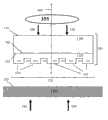
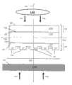
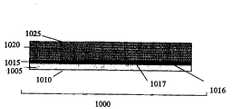
图1A是展示本发明的包含两个聚合物层的复合构图设备的剖面图的示意图。图1B是展示本发明的具有高热稳定性的、包含两个聚合物层的另一个复合构图设备的剖面图的示意图。图1C是展示本发明的具有高热稳定性的、包含三个聚合物层的复合构图设备的剖面图的示意图。图1D是展示本发明的包含四个聚合物层的复合构图设备的剖面图的示意图,所述复合构图设备具有对制造过程中聚合和/或固化导致的图案变形的良好抗性。Figure 1A is a schematic diagram showing a cross-sectional view of a composite patterning device of the present invention comprising two polymer layers. FIG. 1B is a schematic diagram showing a cross-sectional view of another composite patterning device of the present invention comprising two polymer layers having high thermal stability. 1C is a schematic diagram showing a cross-sectional view of a composite patterning device comprising three polymer layers with high thermal stability of the present invention. 1D is a schematic diagram showing a cross-sectional view of a composite patterning device of the present invention comprising four polymer layers with good resistance to pattern distortion caused by polymerization and/or curing during fabrication.
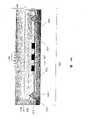
图2A是展示示例性的凸起图案母版以及由该凸起图案母版制得的示例性构图设备的示意图。图2B展示了包含用本发明方法制备的复合印模的示例性构图设备的凸起结构的扫描电子显微图。2A is a schematic diagram showing an exemplary raised pattern master and an exemplary patterning device made from the raised pattern master. Figure 2B shows a scanning electron micrograph of the raised structures of an exemplary patterning device comprising a composite stamp prepared by the method of the present invention.
图3A是说明制造本发明的复合构图设备的方法的示意图。图3B是说明本发明的复合构图设备的一个可选的制备方法的示意图。FIG. 3A is a schematic diagram illustrating a method of manufacturing the composite patterning device of the present invention. Figure 3B is a schematic diagram illustrating an alternative fabrication method of the composite patterning device of the present invention.
图4A展示了说明本发明的包含复合印模的示例性构图设备的示意图,图4B展示了本发明的示例性复合印模的剖面扫描电子显微图。Figure 4A shows a schematic diagram illustrating an exemplary patterning apparatus of the present invention comprising a composite stamp, and Figure 4B shows a cross-sectional scanning electron micrograph of an exemplary composite stamp of the present invention.
图5A和5B展示了将示例性复合印模上的零部件的位置与其在母版上的位置进行对比测量的结果所对应的变形。5A and 5B illustrate deformations corresponding to measurements of the position of a feature on an exemplary composite stamp compared to its position on the master.
图6A和6B展示了说明本发明的复合印模中的凹入区域的下垂趋势降低的顶视光学显微图。图6A对应于常规的单层PDMS印模,图6B对应于本发明的复合印模。Figures 6A and 6B show top view optical micrographs illustrating the reduced tendency to sag of concave regions in composite stamps of the present invention. Figure 6A corresponds to a conventional single layer PDMS stamp and Figure 6B corresponds to a composite stamp of the present invention.
图7展示了在本发明的一个四层复合印模固化后观察到的收缩程度,该复合印模包含第一PDMS层、第二聚酰亚胺层、第三PDMS层以及第四聚酰亚胺层。Figure 7 shows the degree of shrinkage observed after curing of a four-layer composite stamp of the present invention comprising a first PDMS layer, a second polyimide layer, a third PDMS layer and a fourth polyimide layer. amine layer.
图8是对采用本发明复合印模的示例性的纳米转印工艺的图解。Figure 8 is an illustration of an exemplary nanotransfer process using the composite stamp of the present invention.
图9A-D展示了用本发明的复合印模生成的Ti/Au(2nm/20nm)图案的扫描电子显微图。Figures 9A-D show scanning electron micrographs of Ti/Au (2nm/20nm) patterns generated with the composite stamp of the present invention.
图10展示了针对本发明的四层复合构图设备计算的热引发的聚合过程中的变形程度。Figure 10 shows the degree of deformation during thermally induced polymerization calculated for the four-layer composite patterning device of the present invention.
图11A展示了针对两层复合构图设备计算的热引发的聚合过程中的变形程度。图11B是两层构图设备的聚合后曲率半径随着PDMS层厚度变化的曲线图。图11C是两层构图设备的聚合后曲率半径随着固化温度变化的曲线图。Figure 11A shows the degree of deformation during thermally induced polymerization calculated for a two-layer composite patterning device. Figure 1 IB is a graph of the post-polymerization radius of curvature of a two-layer patterned device as a function of PDMS layer thickness. Figure 11C is a graph of post-polymerization radius of curvature of a two-layer patterned device as a function of curing temperature.
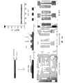
图12A是包含两个h-PDMS层和两个聚酰亚胺(Kapton 
图13A-C展示了本发明的两层复合印模因聚合过程中的热/化学收缩引起的水平变形的计算研究结果。图13A是说明双层复合印模的示意图,所述印模包含一个有效地结合到一个25微米Kapton层上的厚度可变的PDMS层。图13B是预测的水平变形随着PDMS第一层的厚度变化的曲线图。图13C是预测的水平变形随着沿着PDMS第一层外表面的距离变化的曲线图。Figures 13A-C show the results of a computational study of the horizontal deformation of a two-layer composite stamp of the present invention due to thermal/chemical shrinkage during polymerization. Figure 13A is a schematic diagram illustrating a bilayer composite stamp comprising a variable thickness PDMS layer operatively bonded to a 25 micron Kapton layer. Figure 13B is a graph of predicted horizontal deformation as a function of thickness of the first PDMS layer. Figure 13C is a graph of predicted horizontal deformation as a function of distance along the outer surface of the PDMS first layer.
图14A和14B提供了说明本发明的纤维增强复合印模的示意图。图14A提供了剖面图,图14B提供了透视图。图14C提供了分别对应于纤维增强复合印模的第二、第三、第四和第五层的第一、第二、第三和第四选定方向的示意图。Figures 14A and 14B provide schematic diagrams illustrating a fiber reinforced composite stamp of the present invention. Figure 14A provides a cross-sectional view and Figure 14B provides a perspective view. Figure 14C provides a schematic illustration of the first, second, third and fourth selected orientations corresponding to the second, third, fourth and fifth layers, respectively, of the fiber reinforced composite stamp.
图15提供了结合于PDMS层上的复合聚合物层的光学图像。Figure 15 provides an optical image of a composite polymer layer bonded to a PDMS layer.
图16提供了本发明的软复合光掩模的示意图。Figure 16 provides a schematic illustration of a soft composite photomask of the present invention.
图17A展示了本发明的软共形复合光掩模的光学图像,图17B展示了在硅基片上曝光后和显影后的光致抗蚀剂图案的光学图像。Figure 17A shows an optical image of a soft conformal composite photomask of the present invention, and Figure 17B shows an optical image of a photoresist pattern after exposure and development on a silicon substrate.
图18提供了说明本发明的软共形复合光掩模的制备方法的工艺流 程图。Figure 18 provides a process flow diagram illustrating the method of making the soft conformal composite photomask of the present invention.
图19A和19B提供了展示对准系统的示意图,所述对准系统用构图剂(patterning agent)使光掩模和基片对准。Figures 19A and 19B provide schematics showing an alignment system that aligns a photomask and a substrate with a patterning agent.
图20提供了说明本发明的使用构图剂的示例性构图方法的示意图,所述构图剂包含可适应光掩模的光学介质(或墨水)。FIG. 20 provides a schematic diagram illustrating an exemplary patterning method of the present invention using a patterning agent comprising an optical medium (or ink) conformable to a photomask.
具体实施方式Detailed ways
参见附图,相似的数字指示相似的元件,多个图中出现的相同数字指示相同的元件。此外,下文中适用以下定义:Referring to the drawings, like numerals indicate like elements, and like numerals appearing in multiple figures indicate like elements. In addition, the following definitions apply hereinafter:
“热膨胀系数”是表征一种材料在经历温度变化后发生的尺寸变化的参数。线性热膨胀系数是表征一种材料在经历温度变化后发生的长度变化的参数,可以由以下等式表达:The "coefficient of thermal expansion" is a parameter that characterizes the dimensional change that occurs in a material when it undergoes a change in temperature. The coefficient of linear thermal expansion is a parameter that characterizes the length change of a material after experiencing a temperature change, which can be expressed by the following equation:
ΔL=αL0ΔT (I)ΔL=αL0 ΔT (I)
其中ΔL是长度的变化,α是线性热膨胀系数,L0是初始长度,ΔT是温度的变化。本发明提供这样的多层复合构图设备,其中对所述设备中的各层的热性能和物理尺寸进行选择,以使得热膨胀系数在沿着通过该设备延伸的层排列轴线上关于该设备的中心呈基本对称的分布。where ΔL is the change in length, α is the coefficient of linear thermal expansion,L0 is the initial length, and ΔT is the change in temperature. The present invention provides such a multilayer composite patterning device wherein the thermal properties and physical dimensions of the layers in the device are selected such that the coefficient of thermal expansion is relative to the center of the device along the layer arrangement axis extending through the device The distribution is basically symmetrical.
“定位精度”指的是图案转印方法或设备在选定的基片区域中生成图案的能力。“良好的定位精度”指的是方法和设备能够使选定的基片区域中生成的图案与绝对准确定位的空间偏差小于或等于5微米,特别是对于在塑料基片上生成图案的情形。"Location accuracy" refers to the ability of a pattern transfer method or apparatus to generate a pattern in a selected area of a substrate. By "good positioning accuracy" is meant that the method and apparatus are capable of generating patterns in selected substrate regions with a spatial deviation of less than or equal to 5 microns from absolute exact positioning, particularly in the case of patterning on plastic substrates.
“保真度”指的是对转印到基片表面上的图案与构图设备上的凸起图案的相似性的度量。良好的保真度是指,转印到基片表面上的图案与构图设备上的凸起图案的相似性具有偏差小于100纳米的特征。"Fidelity"refers to a measure of the similarity of the pattern transferred onto the substrate surface to the raised pattern on the patterning device. Good fidelity means that the similarity of the pattern transferred onto the substrate surface to the raised pattern on the patterning device is characterized by deviations of less than 100 nanometers.
“杨氏模量”是材料、设备或层的一种机械特性,它指的是一种给定物质的应力与应变之比。杨氏模量可表示为:"Young's modulus" is a mechanical property of a material, device or layer that refers to the ratio of stress to strain for a given substance. Young's modulus can be expressed as:

其中E是杨氏模量,L0是平衡长度,ΔL是施加应力后的长度变化,F是施加的力,A是力的施加面积。杨氏模量也可通过下式用拉梅(Lame) 常数表示:where E is Young's modulus,L0 is the equilibrium length, ΔL is the change in length after stress is applied, F is the force applied, and A is the area on which the force is applied. Young's modulus can also be expressed in terms of Lame's constant by the following formula:
其中λ和μ是拉梅常数。杨氏模量可用单位面积上的单位力表示,例如帕斯卡(Pa=N m-2)。where λ and μ are Lame constants. Young's modulus can be expressed as unit force per unit area, eg Pascal (Pa=N m−2 ).
高杨氏模量(或“高模量”)和低杨氏模量(或“低模量”)是给定的材料、层或设备的杨氏模量大小的比较方式的描述语。在本发明中,高杨氏模量大于低杨氏模量,在某些应用中优选大大约10倍,在其它应用中更优选大于约100倍,在另外的应用中进一步优选大大约1000倍。在一个实施方案中,高杨氏模量的材料具有选自约1GPa至约10GPa范围内的杨氏模量,低杨氏模量的材料具有选自约1MPa至约10MPa范围内的杨氏模量。High Young's modulus (or "high modulus") and low Young's modulus (or "low modulus") are descriptors of how the magnitude of the Young's modulus of a given material, layer or device compares. In the present invention, the high Young's modulus is greater than the low Young's modulus, preferably about 10 times greater in some applications, more preferably greater than about 100 times in other applications, and further preferably about 1000 times greater in other applications . In one embodiment, the high Young's modulus material has a Young's modulus selected from the range of about 1 GPa to about 10 GPa, and the low Young's modulus material has a Young's modulus selected from the range of about 1 MPa to about 10 MPa. quantity.
“共形接触”指的是在表面和/或涂布的表面之间建立的接触,所述接触可用于在基片表面上制造结构。一方面,共形接触涉及复合构图设备的一个或多个接触表面对基片表面的总体形状的宏观适应。另一方面,共形接触涉及复合构图设备的一个或多个接触表面对基片表面的微观适应,所述微观适应导致没有空隙的密切接触。意图使术语共形接触与其在软光刻领域中的使用一致。共形接触可以在复合构图设备的一个或多个裸露接触表面与基片表面之间建立。或者,共形接触可以在复合构图设备的一个或多个涂布的接触表面与基片表面之间建立,例如接触表面上沉积有转印材料和/或构图剂。或者,共形接触可以在复合构图设备的一个或多个裸露的或涂布的接触表面与涂布有材料的基片表面之间建立,所述材料包括例如转印材料、构图剂、固体光致抗蚀剂、预聚物层、液体、薄膜或流体。在本发明的一些实施方案中,本发明的构图设备能够与平面建立共形接触。在本发明的一些实施方案中,本发明的构图设备能够与曲面建立共形接触。在本发明的一些实施方案中,本发明的构图设备能够与粗糙面建立共形接触。在本发明的一些实施方案中,本发明的构图设备能够与光滑面建立共形接触。"Conformal contact" refers to the contact established between surfaces and/or coated surfaces that can be used to fabricate structures on a substrate surface. In one aspect, conformal contact involves the macroscopic adaptation of one or more contacting surfaces of a composite patterning device to the general shape of a substrate surface. Conformal contact, on the other hand, involves microscopic adaptation of one or more contact surfaces of a composite patterning device to a substrate surface, which results in intimate contact without voids. The term conformal contact is intended to be consistent with its usage in the field of soft lithography. Conformal contact can be established between one or more exposed contact surfaces of the composite patterning device and the substrate surface. Alternatively, conformal contact can be established between one or more coated contact surfaces of the composite patterning device and the substrate surface, eg, with a transfer material and/or patterning agent deposited on the contact surface. Alternatively, conformal contact can be established between one or more bare or coated contact surfaces of a composite patterning device and a substrate surface coated with materials including, for example, transfer materials, patterning agents, solid light Resists, prepolymer layers, liquids, films or fluids. In some embodiments of the invention, the patterning devices of the invention are capable of establishing conformal contact with a flat surface. In some embodiments of the invention, the patterning devices of the invention are capable of establishing conformal contact with curved surfaces. In some embodiments of the invention, the patterning devices of the invention are capable of establishing conformal contact with rough surfaces. In some embodiments of the invention, the patterning devices of the invention are capable of establishing conformal contact with smooth surfaces.
“抗弯刚度”是材料、设备或层的一种机械性能,它指的是材料、设备或层变形的能力。抗弯刚度可以表示为:"Bending stiffness" is a mechanical property of a material, device or layer that refers to the ability of the material, device or layer to deform. Bending stiffness can be expressed as:
其中D为抗弯刚度,E为杨氏模量,h为厚度,v为泊松比。抗弯刚度可以表示为单位力与单位长度相乘,例如Nm。Where D is the bending stiffness, E is the Young's modulus, h is the thickness, and v is Poisson's ratio. Bending stiffness can be expressed as unit force multiplied by unit length, eg Nm.
“聚合物”是指包含多个重复化学基团的分子,所述重复化学基团通常称为单体。聚合物通常具有高分子量的特征。可用于本发明的聚合物可以是有机聚合物或无机聚合物,并且可以处于无定形、半无定形(semi-amorphous)、结晶或部分结晶状态。聚合物可以包含具有相同化学组成的单体,或者可以包含具有不同化学组成的多种单体,例如共聚物。具有相连的单体链的交联聚合物对于本发明的一些应用而言特别有用。可用于本发明的方法、设备和设备部件中的聚合物包括,但不限于,塑料、弹性体、热塑性弹性体、弹性塑料、热固性塑料、热塑性塑料以及丙烯酸酯。示例性的聚合物包括,但不限于,缩醛聚合物、可生物降解聚合物、纤维素聚合物(cellulosic polymer)、含氟聚合物、尼龙、聚丙烯腈聚合物、聚酰胺-酰亚胺聚合物、聚酰亚胺、多芳基化合物、聚苯并咪唑、聚丁烯、聚碳酸酯、聚酯、聚醚酰亚胺、聚乙烯、乙烯共聚物以及改性聚乙烯、聚酮、聚甲基丙烯酸甲酯、聚甲基戊烯、聚苯醚以及聚苯硫醚、聚邻苯二甲酰胺、聚丙烯、聚氨酯、苯乙烯树脂、砜基树脂、乙烯基树脂或上述聚合物的任意组合。"Polymer" refers to a molecule comprising multiple repeating chemical groups, commonly referred to as monomers. Polymers are generally characterized by high molecular weight. Polymers useful in the present invention may be organic polymers or inorganic polymers, and may be in an amorphous, semi-amorphous, crystalline or partially crystalline state. A polymer may contain monomers of the same chemical composition, or may contain multiple monomers of different chemical compositions, such as a copolymer. Crosslinked polymers having linked monomer chains are particularly useful for some applications of the present invention. Polymers useful in the methods, apparatus, and apparatus components of the present invention include, but are not limited to, plastics, elastomers, thermoplastic elastomers, elastic plastics, thermosets, thermoplastics, and acrylates. Exemplary polymers include, but are not limited to, acetal polymers, biodegradable polymers, cellulosic polymers, fluoropolymers, nylon, polyacrylonitrile polymers, polyamide-imide Polymers, polyimides, polyarylates, polybenzimidazoles, polybutenes, polycarbonates, polyesters, polyetherimides, polyethylene, ethylene copolymers and modified polyethylenes, polyketones, Polymethyl methacrylate, polymethylpentene, polyphenylene ether and polyphenylene sulfide, polyphthalamide, polypropylene, polyurethane, styrene resin, sulfone-based resin, vinyl resin, or polymers of the above random combination.
“弹性体”指的是能够被拉伸或变形,并能够没有实质性永久变形地回复原形的聚合物材料。弹性体通常发生基本上弹性的变形。可用于本发明的示例性的弹性体可包括聚合物、共聚物、复合材料,或聚合物与共聚物的混合物。弹性体层指的是包括至少一种弹性体的层。弹性体层也可包括掺杂剂或其它非弹性体材料。可用于本发明的弹性体可包括,但不限于,含硅聚合物例如聚硅氧烷,包括聚二甲基硅氧烷(即PDMS和h-PDMS)、聚甲基硅氧烷、部分烷基化的聚甲基硅氧烷、聚烷基甲基硅氧烷和聚苯基甲基硅氧烷,以及硅改性的弹性体;热塑性弹性体、苯乙烯材料、烯属材料、聚烯烃、聚氨酯热塑性弹性体、聚酰胺、合成橡胶、聚异丁烯、聚(苯乙烯-丁二烯-苯乙烯)、聚氨酯、聚氯丁二烯和硅 氧烷。"Elastomeric"refers to a polymeric material capable of being stretched or deformed and returning to its original shape without substantial permanent deformation. Elastomers generally deform substantially elastically. Exemplary elastomers useful in the present invention may include polymers, copolymers, composites, or blends of polymers and copolymers. An elastomeric layer refers to a layer comprising at least one elastomer. The elastomeric layer may also include dopants or other non-elastomeric materials. Elastomers useful in the present invention may include, but are not limited to, silicon-containing polymers such as polysiloxanes, including polydimethylsiloxanes (i.e., PDMS and h-PDMS), polymethylsiloxanes, partial alkanes Siliconated polymethylsiloxanes, polyalkylmethylsiloxanes and polyphenylmethylsiloxanes, and silicon-modified elastomers; thermoplastic elastomers, styrenic materials, olefinic materials, polyolefins , polyurethane thermoplastic elastomer, polyamide, synthetic rubber, polyisobutylene, poly(styrene-butadiene-styrene), polyurethane, polychloroprene, and silicone.
“聚合物层”指的是包含一种或多种聚合物的层。可用于本发明的聚合物层可包含基本纯的聚合物层,或者包含多种不同聚合物的混合物的层。可用于本发明的聚合物层也包括多相聚合物层和/或复合聚合物层,所述多相聚合物层和复合聚合物层包含一种或多种聚合物的组合以及一种或多种附加材料,例如掺杂剂或结构添加剂。这样的附加材料向本发明的聚合物层中的纳入,可用于对聚合物层的机械性能—例如杨氏模量和抗弯刚度—进行选择和调整。附加材料在复合聚合物层中的分布可以是各向同性的、部分各向同性的或各向异性的。可用于本发明的复合聚合物层包含与(i)纤维,例如玻璃纤维或聚合物纤维,(ii)颗粒,例如硅颗粒和/或纳米颗粒,和/或(iii)其它结构增强剂复合的一种或多种聚合物。在本发明的一个实施方案中,具有高杨氏模量的聚合物层包含具有选自约1GPa至约10GPa范围内的杨氏模量的聚合物。示例性的高杨氏模量聚合物层可包含聚酰亚胺、聚酯、聚醚醚酮、聚醚砜、聚醚酰亚胺、聚对苯二甲酸乙二醇酯、聚酮、聚苯硫醚、这些材料的任意组合或者其它具有类似机械性能的聚合物材料。在本发明的一个实施方案中,具有低杨氏模量的聚合物层包含具有选自约1MPa至约10MPa范围内的杨氏模量的聚合物。示例性的低杨氏模量聚合物层可包含弹性体,例如PDMS、h-PDMS、聚丁二烯、聚异丁烯、聚(苯乙烯-丁二烯-苯乙烯)、聚氨酯、聚氯丁二烯和硅氧烷。"Polymer layer" refers to a layer comprising one or more polymers. Polymer layers useful in the present invention may comprise layers of substantially pure polymers, or layers comprising mixtures of various polymers. Polymer layers useful in the present invention also include multiphase polymer layers and/or composite polymer layers comprising combinations of one or more polymers and one or more An additional material, such as a dopant or a structural additive. The incorporation of such additional materials into the polymer layers of the present invention can be used to select and tune the mechanical properties of the polymer layers, such as Young's modulus and flexural stiffness. The distribution of additional material in the composite polymer layer may be isotropic, partially isotropic or anisotropic. Composite polymer layers useful in the present invention comprise composite polymeric polymers composited with (i) fibers, such as glass fibers or polymeric fibers, (ii) particles, such as silicon particles and/or nanoparticles, and/or (iii) other structural reinforcing agents. one or more polymers. In one embodiment of the present invention, the polymer layer having a high Young's modulus comprises a polymer having a Young's modulus selected from the range of about 1 GPa to about 10 GPa. Exemplary high Young's modulus polymer layers may include polyimide, polyester, polyetheretherketone, polyethersulfone, polyetherimide, polyethylene terephthalate, polyketone, poly Diphenylene sulfide, any combination of these materials, or other polymeric materials with similar mechanical properties. In one embodiment of the present invention, the polymer layer having a low Young's modulus comprises a polymer having a Young's modulus selected from the range of about 1 MPa to about 10 MPa. Exemplary low Young's modulus polymer layers may comprise elastomers such as PDMS, h-PDMS, polybutadiene, polyisobutylene, poly(styrene-butadiene-styrene), polyurethane, polychloroprene alkenes and siloxanes.
“复合”指的是材料、层或设备含有一种以上的组分,例如一种以上的材料和/或相。本发明提供包含多个聚合物层的复合构图设备,各层具有不同的化学组成和机械性能。本发明的复合聚合物层包括这样的层,所述层包含一种或多种聚合物与纤维(例如玻璃或弹性体纤维)、颗粒(例如纳米颗粒或微米颗粒)或其任意组合的组合。"Composite" means that a material, layer or device contains more than one component, such as more than one material and/or phase. The present invention provides composite patterning devices comprising multiple polymer layers, each layer having a different chemical composition and mechanical properties. Composite polymer layers of the present invention include layers comprising one or more polymers in combination with fibers (eg, glass or elastomeric fibers), particles (eg, nanoparticles or microparticles), or any combination thereof.
“弹性体”指的是能够被拉伸或变形,并能够没有实质性永久变形地回复原形的聚合物材料。弹性体通常发生基本上弹性的变形。可用于本发明的示例性的弹性体可包括聚合物、共聚物、复合材料,或聚合物与共聚物的混合物。弹性体层指的是包含至少一种弹性体的层。弹性体层也可包含掺杂剂或其它非弹性体材料。可用于本发明的弹性体可包括,但不限于,PDMS、h-PDMS、聚丁二烯、聚异丁烯、聚(苯乙烯-丁二烯- 苯乙烯)、聚氨酯、聚氯丁二烯以及硅氧烷。"Elastomeric"refers to a polymeric material capable of being stretched or deformed and returning to its original shape without substantial permanent deformation. Elastomers generally deform substantially elastically. Exemplary elastomers useful in the present invention may include polymers, copolymers, composites, or blends of polymers and copolymers. An elastomeric layer refers to a layer comprising at least one elastomer. The elastomeric layer may also contain dopants or other non-elastomeric materials. Elastomers useful in the present invention may include, but are not limited to, PDMS, h-PDMS, polybutadiene, polyisobutylene, poly(styrene-butadiene-styrene), polyurethane, polychloroprene, and silicon oxane.
术语“电磁辐射”指的是电场和磁场波。可用于本发明方法的电磁辐射包括,但不限于,伽马射线、X射线、紫外光、可见光、红外光、微波、无线电波或这些电磁辐射的任意组合。The term "electromagnetic radiation" refers to electric and magnetic field waves. Electromagnetic radiation that can be used in the methods of the present invention includes, but is not limited to, gamma rays, X-rays, ultraviolet light, visible light, infrared light, microwaves, radio waves, or any combination of these electromagnetic radiations.
术语“强度”指的是一个或多个电磁波的振幅的平方。此处的振幅指的是电磁波的振动幅度。或者,术语“强度”可以指一个或多个电磁辐射束的时均能量通量,例如一个或多个电磁辐射束的每平方厘米、每单位时间的光子数。The term "intensity" refers to the square of the amplitude of one or more electromagnetic waves. The amplitude here refers to the vibration amplitude of the electromagnetic wave. Alternatively, the term "intensity" may refer to the time-averaged energy flux of the one or more beams of electromagnetic radiation, eg, the number of photons per square centimeter, per unit of time, of the one or more beams of electromagnetic radiation.
“致动器”指的是能够提供力和/或移动某物和/或控制某物的设备、设备部件或元件。本发明的示例性的致动设备能够产生力,例如用于使构图设备与基片表面形成接触、例如共形接触的力。"Actuator" refers to a device, device part or element capable of providing force and/or moving and/or controlling something. Exemplary actuation devices of the present invention are capable of generating a force, eg, for bringing a patterning device into contact, eg, conformal contact, with a substrate surface.
“层”指的是本发明的复合构图设备的一种元件。示例性的层具有这样的物理尺寸和机械性能,该尺寸和性能使复合构图设备能够在基片表面上生成具有出色的保真度和良好的定位精度的图案。本发明的层可以是连续或单一的形体,或不连续形体的集合,例如凸起零部件的集合。本发明的层可以具有均匀的组成或不均匀的组成。本发明的一个实施方案提供包含多个层—例如多个聚合物层—的复合构图设备。本发明的层可以用沿着通过构图设备延伸的层排列轴线方向的厚度进行表征,所述轴线包括例如与含有一个或多个接触表面的平面垂直的层排列轴线。"Layer" refers to an element of the composite patterning device of the present invention. Exemplary layers have physical dimensions and mechanical properties that enable the composite patterning device to generate patterns on the substrate surface with excellent fidelity and good positioning accuracy. A layer of the invention may be a continuous or unitary feature, or a collection of discrete features, such as a collection of raised features. The layers of the present invention may have a uniform composition or a non-uniform composition. One embodiment of the invention provides a composite patterning device comprising multiple layers, such as multiple polymer layers. Layers of the invention may be characterized by thickness along a layer arrangement axis extending through the patterning device, including, for example, a layer arrangement axis perpendicular to a plane containing one or more contact surfaces.
“热稳定”指的是设备或设备部件在不损失特有性能—例如凸起图案的凸起零部件的物理尺寸和空间分布—的情况下承受温度变化的特性。"Thermal stability" refers to the property of a device or device part to withstand temperature changes without loss of characteristic properties, such as physical size and spatial distribution of raised features of a raised pattern.
“热膨胀系数关于构图设备中心呈基本对称的分布”指的是一种设备布置方式,在该布置方式中,对组成构图设备的一个或多个层的机械性能和热性能的选择使得在沿着层排列轴线上,例如与包含一个或多个接触表面的平面垂直的层排列轴线上关于构图设备中心呈基本对称的分布。在一个实施方案中,热膨胀系数具有关于构图设备中心对称的特征,其中与绝对对称分布的偏差小于大约10%。在另一个实施方案中,热膨胀系数具有关于构图设备中心对称的特征,其中与绝对对称分布的偏差小于大约5%。"Substantially symmetrical distribution of coefficients of thermal expansion about the center of the patterning device" refers to a device arrangement in which the mechanical and thermal properties of one or more layers making up the patterning device are chosen such that The distribution on the axis of the layer arrangement, for example perpendicular to the plane containing the one or more contact surfaces, is substantially symmetrical with respect to the center of the patterning device. In one embodiment, the coefficient of thermal expansion has a characteristic that is symmetrical about the center of the patterning device, wherein the deviation from an absolutely symmetrical distribution is less than about 10%. In another embodiment, the coefficient of thermal expansion has a characteristic that is symmetrical about the center of the patterning device, wherein the deviation from an absolutely symmetrical distribution is less than about 5%.
“有效地结合”指的是本发明的复合构图设备的层和/或设备部件的 一种布置。有效地结合的层或设备部件,例如第一、第二、第三和/或第四聚合物层,指的是一种布置方式,在该布置方式中,施加于一个层或设备部件上的力传递给另一个层或设备部件。有效地结合的层或设备部件可以处于接触中,例如层的内表面和/或外表面处于直接接触。或者,有效地结合的层或设备部件可以由一个或多个位于两层或两个设备部件的内表面和/或外表面之间的连接层连接,例如由薄金属层连接。"Effectively combined" refers to an arrangement of layers and/or device components of the composite patterning device of the present invention. Effectively bonded layers or device components, such as first, second, third and/or fourth polymer layers, refer to an arrangement in which the The force is transmitted to another layer or device part. The operatively bonded layers or device components may be in contact, eg inner and/or outer surfaces of the layers are in direct contact. Alternatively, operatively bonded layers or device parts may be joined by one or more connecting layers, such as by a thin metal layer, between the inner and/or outer surfaces of two layers or two device parts.
在以下叙述中,为了提供对本发明的确切实质的详尽解释,提出了本发明的设备、设备部件和方法的大量具体细节。然而对于本领域技术人员而言明显的是,本发明可以在没有这些具体细节的情况下实施。In the following description, in order to provide a thorough explanation of the precise substance of the invention, numerous specific details are set forth in the apparatus, apparatus parts and methods of the invention. It will be apparent, however, to one skilled in the art that the present invention may be practiced without these specific details.
本发明提供用于在基片表面上制作图案—例如包含微米结构和/或纳米级结构的图案—的方法、设备和设备部件。本发明提供复合构图设备,例如印模、塑模和光掩模,这些设备具有增强的热稳定性以及对固化引起的图案变形的抗性。本发明的方法、设备和设备部件能够生成具有良好的保真度和出色的定位精度的高分辨率图案。The present invention provides methods, apparatus and apparatus components for fabricating patterns, eg, patterns comprising microstructures and/or nanoscale structures, on the surface of a substrate. The present invention provides composite patterning devices, such as stamps, molds, and photomasks, that have enhanced thermal stability and resistance to pattern distortion caused by curing. The methods, devices and device components of the present invention are capable of generating high resolution patterns with good fidelity and excellent positioning accuracy.
图1A是展示本发明的包含两个聚合物层的复合构图设备的剖面图的示意图。图示的复合构图设备100包含低杨氏模量的第一聚合物层110和高杨氏模量的第二聚合物层120。第一聚合物层110包含三维凸起图案125,该图案125具有由多个凹入区域134分隔的多个凸起零部件133。第一聚合物层110还具有位置与内表面135相对的多个接触表面130。本发明包括接触表面130处于同一平面内的实施方案,以及接触表面130处于多个平面内的实施方案。第二聚合物层120具有内表面140和外表面150。在图1A所示的实施方案中,第一聚合物层110的内表面135与第二聚合物层120的内表面140接触。任选地,第二聚合物层120有效地连接至致动器155,所述致动器155能够将力(如箭头156所示意性表示)引向外表面150上。Figure 1A is a schematic diagram showing a cross-sectional view of a composite patterning device of the present invention comprising two polymer layers. The illustrated
可以将任何能够使施加于外表面150上的力有效传递给接触表面130的方式将第一聚合物层110和第二聚合物层120结合。在示例性的实施方案中,通过组成各层的聚合物之间的共价连接使第一聚合物层110和第二聚合物层120结合。或者,可以通过各层之间的分子间引力,例如范德华力、偶极-偶极力、氢键和伦敦力,使第一聚合物层110和第二聚合物层120结合。或者,可以通过外部的层对准系统,例如夹持、 紧固和/或螺栓连接系统,使第一聚合物层110和第二聚合物层120结合。或者,可以使用一个或多个位于内表面135和内表面140之间的连接层(未示于图1A中),例如薄金属层,使第一聚合物层110和第二聚合物层120结合。对于一些应用,优选通过强的共价结合和/或分子间引力使第一聚合物层110和第二聚合物层120结合,因为这样使凸起零部件133和凹入区域134具有良好的机械刚性,还提供了一种使施加于外表面150上的力均匀地向接触表面130分布的有效方法。
在图1A所示的示例性实施方案中,对第一聚合物层110的组成、杨氏模量和/或沿着与接触表面130所处平面垂直的层排列轴线160方向上的厚度进行选择,以使构图设备100具有这样的机械性能,该机械性能使其能够制造高分辨率的、图案变形降低的微米级和/或纳米级结构的图案。此外,也可以对第一聚合物层110和第二聚合物层120的杨氏模量和/或厚度进行选择,使得可以将构图设备100容易地结合到商品化的印刷和模塑系统中。在一个示例性的实施方案中,第一聚合物层110包括一个PDMS层,该PDMS层沿着层排列轴线160的厚度选自约5微米至约10微米范围内。第一聚合物层110的厚度也可定义为第二聚合物层120的内表面140与接触表面130之间的最短距离。在一个示例性的实施方案中,第二聚合物层120包括一个聚酰亚胺层,该聚酰亚胺层沿着层排列轴线的厚度等于约25微米。第二聚合物层120的厚度也可定义为第二聚合物层120的外表面150与内表面140之间的最短距离。In the exemplary embodiment shown in FIG. 1A, the composition, Young's modulus, and/or thickness of the
为制造包含一个或多个结构的图案,使复合构图设备100与基片180的表面185彼此接触,该接触优选使接触表面130的至少一部分与基片表面185之间建立共形接触。可以通过使构图设备100移动至与基片180接触的方式在外表面150上施加外力(由箭头156示意性表示),实现这些表面之间的共形接触。或者,可以通过使基片180移动至与构图设备100接触的方式在基片180上施加外力(由箭头190示意性表示)。本发明还包括这样的实施方案,其中通过这些力(156和190)和基片180和构图设备100的移动的结合建立共形接触。To fabricate a pattern comprising one or more structures,
图1B是展示本发明的具有高热稳定性的、包含两个聚合物层的另一个复合构图设备的剖面图的示意图。如图1B所示,复合构图设备200包含具有低杨氏模量的不连续的第一聚合物层210,第一聚合物层210 有效地连结于具有高杨氏模量的第二聚合物层120上。在该实施方案中,不连续的第一聚合物层210包含三维凸起图案225,所述凸起图案包含由多个凹入区域234分隔的多个分立的凸起零部件233。如图1B所示,分立的凸起零部件233彼此不接触,但各自有效地结合到第二聚合物层120上。包含多个分立的凸起零部件的第一聚合物层在本发明的复合构图设备中的纳入是有利的,因为这样降低了第一和第二聚合物层210和120的热膨胀性能之间的不匹配程度,还降低了第一聚合物层210中的材料的净用量,所述第一聚合物层210可包含一种高热膨胀系数的材料,例如PDMS。FIG. 1B is a schematic diagram showing a cross-sectional view of another composite patterning device of the present invention comprising two polymer layers having high thermal stability. As shown in FIG. 1B, the composite patterning device 200 comprises a discontinuous first polymer layer 210 having a low Young's modulus, the first polymer layer 210 being effectively bonded to a second polymer layer having a high Young's modulus. 120 on. In this embodiment, the discontinuous first polymer layer 210 comprises a three-dimensional raised pattern 225 comprising a plurality of discrete raised features 233 separated by a plurality of recessed regions 234 . As shown in FIG. 1B , the discrete raised features 233 do not contact each other, but are each operatively bonded to the
图1C是展示本发明的具有高热稳定性的、包含三个聚合物层的另一个复合构图设备的剖面图的示意图。图示的复合构图设备300进一步包括具有内表面315和外表面320的第三聚合物层310。在图1C中所示的实施方案中,第三聚合物层310的内表面315与第二聚合物层120的外表面150接触。任选地,第三聚合物层310有效地结合于致动器155上,所述致动器能够将力(如箭头156所示意性表示)引向外表面320上。1C is a schematic diagram showing a cross-sectional view of another composite patterning device of the present invention comprising three polymer layers with high thermal stability. The illustrated
在图1C所示的实施方案中,第三聚合物层310沿层排列轴线160的厚度330近似等于第一聚合物层110沿层排列轴线160的厚度340,对于一些应用,优选两厚度之差在10%之内。在该实施方案中,对具有相同或相似(例如差别在10%之内)的热膨胀系数的第三聚合物层310和第一聚合物层110的选择—例如两层均包含PDMS层,得到高热稳定性和对温度变化引起的图案变形的抗性。特别是,这样的布置使得热膨胀系数在沿着层排列轴线160上关于构图设备300的中心(由中心线轴350标明)呈基本对称的分布。热膨胀系数的对称分布使得温度改变后生成反向作用的力,这使得凸起图案125、凸起零部件133和接触表面130的拉伸、翘曲、弯曲、膨胀和压缩的程度最小化。In the embodiment shown in FIG. 1C, the
图1D是展示本发明的一个四层复合构图设备的剖面图的示意图,所述复合构图设备具有对制造过程中聚合和/或固化导致的图案变形的良好抗性。图示的复合构图设备400进一步包括具有内表面415和外表面420的第四聚合物层410。在图1D所示的实施方案中,第四聚合物层410的内表面415与第三聚合物层310的外表面320接触。任选地,第四聚合物层410有效地结合于致动器155上,所述致动器能够将力(如箭头 156所示意性表示)引向外表面420上。1D is a schematic diagram showing a cross-sectional view of a four-layer composite patterning device of the present invention having good resistance to pattern distortion caused by polymerization and/or curing during fabrication. The illustrated
在图1D所示的实施方案中,第三聚合物层310沿层排列轴线160的厚度330近似等于第一聚合物层110沿层排列轴线160的厚度340,对于一些应用,优选两厚度之差在10%之内;并且第四聚合物层410沿层排列轴线160的厚度430近似等于第二聚合物层120沿层排列轴线160的厚度440,对于一些应用,优选两厚度之差在10%之内。在该实施方案中,对具有相同的热膨胀系数和杨氏模量的第三聚合物层310和第一聚合物层110的选择—例如两层均包含PDMS层,以及对具有相同的热膨胀系数和杨氏模量的第四聚合物层410和第二聚合物层120的选择—例如两层均包含聚酰亚胺层,得到对制造过程中聚合和/或固化导致的图案变形的良好抗性。特别是,这样的布置使得凸起图案125和接触表面130在聚合和/或固化过程中的拉伸、翘曲、弯曲、膨胀和压缩的程度最小化。In the embodiment shown in FIG. 1D, the
本发明的包括第一、第二、第三和第四层在内的聚合物层的表面可以具有特定的凸起图案,例如对准通道和/或槽,用于在层之间提供适当的对准作用。或者,本发明的聚合物层的表面可以具有特定的凸起图案,例如对准通道和/或槽,用于在复合构图设备和具有互补的(即啮合的)通道和/或槽的致动器之间提供适当的对准作用,所述致动器包括例如印刷设备、模塑设备或接触光刻装置。或者,本发明的聚合物层的表面可以具有特定的凸起图案,例如对准通道和/或槽,用于在复合构图设备和具有互补的(即啮合的)通道和/或槽的基片表面之间提供适当的对准作用。本领域技术人员会理解,使用这种“锁和钥匙”的对准机制、通道、槽以及系统是微制造领域中公知的,可以容易地纳入本发明的构图设备中。The surfaces of the polymeric layers of the present invention, including the first, second, third and fourth layers, may have specific raised patterns, such as aligned channels and/or grooves, for providing proper spacing between the layers. Alignment effect. Alternatively, the surface of the polymer layer of the present invention may have a specific raised pattern, such as aligned channels and/or grooves, for actuation in composite patterning devices and have complementary (i.e., intermeshed) channels and/or grooves. Proper alignment is provided between actuators such as printing devices, molding devices or contact lithography devices. Alternatively, the surface of the polymer layer of the present invention may have a specific raised pattern, such as alignment channels and/or grooves, for use in composite patterning devices and substrates with complementary (i.e., engaging) channels and/or grooves. Provide proper alignment between surfaces. Those skilled in the art will appreciate that alignment mechanisms, channels, slots and systems using such "locks and keys" are well known in the art of microfabrication and can be readily incorporated into the patterning apparatus of the present invention.
对本发明的复合构图设备中的聚合物层的组成、物理尺寸和机械性能的选择在很大程度上取决于所使用的材料转印方法(例如印刷、模塑等)以及待制造的结构/图案的物理尺寸。从这个意义上说,可以认为,本发明的复合构图设备的规格可以针对待实现的具体功能任务或图案/结构尺寸进行选择性调整。例如,可用于通过软光刻方法印刷纳米级结构的本发明的两层构图设备,可以包含厚度选自约1微米至约5微米范围内的第一聚合物弹性体层,以及包含聚酰亚胺层的、厚度小于或等于约25微米的第二聚合物层。与之相比,可用于微模塑制造尺寸在约10 微米至约50微米范围内的结构的本发明两层构图设备,可以包含厚度选自约20微米至约60微米范围内的第一聚合物弹性体层,以及包含聚酰亚胺层的、厚度选自约25微米至约100微米范围内的第二聚合物层。The choice of composition, physical dimensions and mechanical properties of the polymer layer in the composite patterning device of the present invention depends largely on the material transfer method used (e.g. printing, molding, etc.) and the structure/pattern to be fabricated physical size. In this sense, it can be considered that the specifications of the composite patterning device of the present invention can be selectively adjusted for specific functional tasks or pattern/structure dimensions to be realized. For example, a two-layer patterning device of the present invention useful for printing nanoscale structures by soft lithographic methods may comprise a first polymeric elastomer layer having a thickness selected from the range of about 1 micron to about 5 microns, and a layer comprising polyimide A second polymer layer of the amine layer having a thickness less than or equal to about 25 microns. In contrast, a two-layer patterning device of the present invention usable for micromolding to produce structures having dimensions in the range of about 10 microns to about 50 microns may comprise a first polymeric layer having a thickness selected from the range of about 20 microns to about 60 microns A bioelastomer layer, and a second polymer layer comprising a polyimide layer having a thickness selected from the range of about 25 microns to about 100 microns.
本发明的复合构图设备,例如印模、塑模和光掩模,可以通过材料科学、软光刻和光刻领域中的任何已知方法制得。本发明的一个示例性的构图设备由下述方法制得:通过将聚二甲基硅氧烷(PDMS)预聚物(DowCorning Sylgard 184)浇注于凸起图案母版上并使其固化而制得包含弹性体的第一聚合物层,所述凸起图案母版是通过常规光刻方法制备的、由光致抗蚀剂(Shipley 1805)的图案化零部件所组成的凸起图案母版。对于可用于本发明的凸起图案母版,在零部件大于约2微米的情况下,可以采用常规的接触模式光刻法制备,在零部件小于约2微米的情况下,可以采用电子束光刻法制备。在一个示例性方法中,将PDMS(来自DowCorning的Sylgard 184)或h-PDMS(VDT-731,Gelest公司)混合并脱气,浇注于母版上并在约80摄氏度下、在烘箱中固化。或者,可以额外使用固化剂在室温下进行184PDMS的固化。优选在高模量第二层—例如聚酰亚胺层—的存在下使包含PDMS或h-PDMS的第一聚合物层固化,以降低固化和/或聚合引起的收缩。在一个实施方案中,先使聚酰亚胺层的内表面变粗糙,然后再与PDMS预聚物接触,以增强PDMS预聚物固化后第一PDMS层与第二聚酰亚胺层的结合力。聚酰亚胺层的表面粗糙化可以通过本领域任何已知方法实现,包括使聚酰亚胺内表面暴露于等离子体。The composite patterning devices of the present invention, such as stamps, molds and photomasks, can be fabricated by any known method in the fields of materials science, soft lithography and photolithography. An exemplary patterning device of the present invention is made by casting a polydimethylsiloxane (PDMS) prepolymer (Dow Corning Sylgard 184) onto a raised pattern master and allowing it to cure A first polymer layer comprising an elastomer was obtained, and the raised pattern master was prepared by conventional photolithographic methods and consisted of patterned features of photoresist (Shipley 1805) . Raised pattern masters useful in the present invention can be prepared by conventional contact-mode photolithography for features larger than about 2 microns, and by electron beam photolithography for features smaller than about 2 microns. Engraved preparation. In one exemplary method, PDMS (Sylgard 184 from Dow Corning) or h-PDMS (VDT-731, Gelest Corporation) was mixed and degassed, cast on a master and cured in an oven at about 80 degrees Celsius. Alternatively, curing of 184PDMS can be performed at room temperature with the additional use of a curing agent. The first polymer layer comprising PDMS or h-PDMS is preferably cured in the presence of a high modulus second layer, such as a polyimide layer, to reduce curing and/or polymerization induced shrinkage. In one embodiment, the inner surface of the polyimide layer is roughened prior to contacting the PDMS prepolymer to enhance the bonding of the first PDMS layer to the second polyimide layer after the PDMS prepolymer is cured force. Surface roughening of the polyimide layer can be accomplished by any method known in the art, including exposing the inner polyimide surface to plasma.
优选使复合构图设备中的附加层—例如高模量的第二聚合物层—的制备和固化与第一弹性体层的制备同时完成,以使第一弹性体层的凸起图案和接触表面因固化和/或聚合引起的收缩的程度最小化。或者,可以用粘合剂或连接层,例如薄金属层,将高模量第二聚合物层—例如聚酰亚胺层—结合到第一聚合物层上。Preparation and curing of additional layers in the composite patterning device, such as a high modulus second polymer layer, is preferably done simultaneously with the preparation of the first elastomeric layer so that the raised pattern and contact surface of the first elastomeric layer The extent of shrinkage due to curing and/or polymerization is minimized. Alternatively, an adhesive or tie layer, such as a thin metal layer, may be used to bond a high modulus second polymer layer, such as a polyimide layer, to the first polymer layer.
示例性的凸起图案母版是用正性光致抗蚀剂(positivephotoresist,S1818,Shipley)和剥离抗蚀剂(lift off resist)(LOR1A;micron Chem.)制备的。在该示例性方法中,将约450微米厚的测试级硅晶片(Montco Silicon Technologies)用丙酮、异丙醇和去离子水清洗,然后在150摄氏度的热板上干燥10分钟。以3000rpm的 转速旋涂LOR 1A树脂30秒,然后在130摄氏度的热板上预烘干5分钟。接下来,以3000rpm的转速旋涂S1818树脂30秒,然后在110摄氏度的热板上烘干5分钟。将得到的双层膜(约1.7微米厚)用铬离子玻璃掩模、用光学接触光刻机(Suss Microtech MJB3)曝光(□=365nm,16.5mW/cm2)7秒,然后显影(MF-319;Shipley)75秒。显影将所有曝光的S1818抗蚀剂去除。它也大致以各向同性的方式将曝光和未曝光区域中的LOR 1A去除。该工艺的结果是得到S1818在LOR 1A上的图案,其中在曝光区域是裸露的基片区域,并且在图案的边缘有轻微的底切。采用将PDMS浇注到凸起图案母版上并固化的标准软光刻工艺,由该凸起图案母版制备了包含印模的复合构图设备。图2A是展示示例性的凸起图案母版461以及由该凸起图案母版制得的示例性构图设备463的示意图。图2B展示了用本发明方法制备的包含复合印模的示例性构图设备的凸起结构的扫描电子显微图。An exemplary raised pattern master was prepared with a positive photoresist (S1818, Shipley) and a lift off resist (LORIA; micron Chem.). In this exemplary method, approximately 450 micron thick test grade silicon wafers (Montco Silicon Technologies) were cleaned with acetone, isopropanol, and deionized water, then dried on a hot plate at 150 degrees Celsius for 10 minutes. Spin coat LOR 1A resin at 3000 rpm for 30 seconds, then pre-bake on a hot plate at 130°C for 5 minutes. Next, the S1818 resin was spin-coated at 3000rpm for 30 seconds, and then dried on a hot plate at 110°C for 5 minutes. The resulting bilayer film (about 1.7 micron thick) was exposed (□=365nm, 16.5mW/cm2 ) for 7 seconds with a chromium-ion glass mask, an optical contact lithography machine (Suss Microtech MJB3), and then developed (MF- 319; Shipley) 75 seconds. Development removes all exposed S1818 resist. It also removes LOR 1A in both exposed and unexposed regions in a roughly isotropic manner. The result of this process is a pattern of S1818 on LOR 1A, where the exposed areas are bare substrate areas and there is a slight undercut at the edge of the pattern. A composite patterning device including a stamp was fabricated from the raised pattern master using standard soft lithography processes in which PDMS was cast onto the raised pattern master and cured. FIG. 2A is a schematic diagram showing an exemplary raised
图3A是说明制造本发明的复合构图设备的方法的示意图。如图3A的工艺步骤A中所示,可以通过将PDMS的预聚物旋涂于硅上的包含树脂凸起零部件的凸起图案母版上而制得构图设备。任选地,可以用材料的自组装单层膜处理凸起图案母版,以将第一PDMS层对母版的附着力最小化。如图3A的工艺步骤B中所示,可以通过用热板固化若干小时制得第一PDMS层,其中固化温度在约60至约80摄氏度之间。固化后,通过电子束蒸发方法将钛薄膜、金薄膜或两者的组合沉积在第一PDMS层的内表面上,如图3A的工艺步骤C中所示。也可以将钛、金或两者的混合物的薄膜沉积在高模量第二聚合物层的内表面上(见图3A的步骤C)。通过将第一和第二层的覆有涂层的内表面冷焊而将第一和第二层有效地结合,并可以将复合构图设备从凸起图案母版上分离,如图3A的工艺步骤D和E中所分别表示。FIG. 3A is a schematic diagram illustrating a method of manufacturing the composite patterning device of the present invention. As shown in process step A of Figure 3A, a patterned device can be fabricated by spin-coating a prepolymer of PDMS onto a raised pattern master containing resin raised features on silicon. Optionally, the raised pattern master can be treated with a self-assembled monolayer of material to minimize adhesion of the first PDMS layer to the master. As shown in process step B of Figure 3A, the first PDMS layer can be produced by curing with a hot plate for several hours, wherein the curing temperature is between about 60 and about 80 degrees Celsius. After curing, a thin film of titanium, a thin film of gold, or a combination of both was deposited on the inner surface of the first PDMS layer by electron beam evaporation method, as shown in process step C of Figure 3A. A thin film of titanium, gold, or a mixture of the two can also be deposited on the inner surface of the high modulus second polymer layer (see step C of Figure 3A). The first and second layers are effectively bonded by cold welding the coated inner surfaces of the first and second layers, and the composite patterning device can be separated from the raised pattern master, as in the process of Figure 3A Indicated in steps D and E, respectively.
图3B展示了本发明的复合多层构图设备的一个可选的制备方法。如图3B的工艺步骤A中所示,将高模量第二层的内表面用钛、二氧化硅或两者的组合涂布。使高模量第二层的覆有涂层的内侧与用PDMS预聚物旋涂的凸起图案母版接触,并向高模量第二层的外表面施加压力,如图3B的工艺步骤B中所示。该布置使得可以通过旋转凸起图案母版,和/或通过用平的或基于摇杆(rocker based)的压具向高模量第二层施加压力来选择性调整PDMS预聚物层的厚度。在获得所需的厚度后,将PDMS预聚物用约60至80摄氏度范围内的固化温度在烘箱中固化几小时,以形成PDMS第一层,如图3B的工艺步骤C中所示。最后,将复合构图设备与凸起图案母版分离。任选地,该方法包括用材料的自组装单层膜处理凸起图案母版的步骤,以使PDMS第一层与母版的附着力最小化。FIG. 3B shows an alternative fabrication method of the composite multilayer patterning device of the present invention. As shown in process step A of Figure 3B, the inner surface of the high modulus second layer is coated with titanium, silica, or a combination of both. The coated inner side of the high modulus second layer is brought into contact with the raised pattern master spin-coated with PDMS prepolymer, and pressure is applied to the outer surface of the high modulus second layer, as in the process step of Figure 3B Shown in B. This arrangement allows selective adjustment of the thickness of the PDMS prepolymer layer by rotating the raised pattern master, and/or by applying pressure to the high modulus second layer with a flat or rocker based press . After obtaining the desired thickness, the PDMS prepolymer was cured in an oven for several hours with a curing temperature in the range of about 60 to 80 degrees Celsius to form the first PDMS layer, as shown in process step C of Figure 3B. Finally, the composite patterning device is separated from the raised pattern master. Optionally, the method includes the step of treating the raised pattern master with a self-assembled monolayer of material to minimize adhesion of the PDMS first layer to the master.
本说明书中使用的术语和表达方式用于说明而非限制,在这些术语和表达方式的使用中,并没有意图要排除所示的和所述的特征或其部分的任何等同物,而是应当认识到,在本发明要求保护的范围内,可能存在各种变形。因此应当理解的是,虽然通过优选实施方案、示例性实施方案和任选特征对本发明进行了具体的公开,但是本领域技术人员可能采取本说明书公开的概念的变型或变体,因此这样的变型和变体被视为在所附的权利要求限定的本发明范围之内。本说明书给出的具体实施方案是本发明的有用的实施方案的实例,对于本领域技术人员而言显而易见的是,可以采用本说明书公开的设备、设备部件、方法步骤的许多变体实施本发明。可用于本发明的方法和设备可以包括大量任选的设备元件和部件,包括附加聚合物层、玻璃层、陶瓷层、金属层、微流体通道和元件、致动器例如辊压印刷机和柔版印刷机,操作元件(handleelement)、光纤元件、双折射元件例如四分之一波片和半波片,滤光器例如FP标准器、高通截止滤光器和低通截止滤光器,光学放大器、准直元件、准直透镜、反射器、衍射光栅、聚焦元件例如聚焦透镜和反射器,反射器、偏振器、光纤耦合器和发射机、温度控制器、温度传感器、宽带光源和窄带光源。The terms and expressions used in this specification are for the purpose of illustration and not limitation. In the use of these terms and expressions, it is not intended to exclude any equivalents of the features shown and described or parts thereof, but should It is recognized that various modifications are possible within the scope of the claimed invention. It should therefore be understood that although the invention has been specifically disclosed in terms of preferred embodiments, exemplary embodiments and optional features, those skilled in the art may adopt variations or variations of the concepts disclosed in this specification, so such variations and modifications are considered to be within the scope of the invention as defined by the appended claims. The specific embodiments given in this description are examples of useful embodiments of the present invention, and it will be obvious to those skilled in the art that many variants of the equipment, equipment parts, and method steps disclosed in this specification can be used to implement the present invention . Methods and devices useful in the present invention may include a number of optional device elements and components, including additional polymer layers, glass layers, ceramic layers, metal layers, microfluidic channels and elements, actuators such as roll presses and flexo Plate printing machines, handle elements, optical fiber elements, birefringent elements such as quarter-wave plates and half-wave plates, filters such as FP etalons, high-pass cut filters and low-pass cut filters, optics Amplifiers, collimating elements, collimating lenses, reflectors, diffraction gratings, focusing elements such as focusing lenses and reflectors, reflectors, polarizers, fiber optic couplers and transmitters, temperature controllers, temperature sensors, broadband light sources and narrowband light sources .
将本申请中引用的所有参考文献的全部内容通过引用的方式以不与本申请所公开的内容矛盾的程度纳入本说明书。对于本领域技术人员而言显而易见的是,本说明书具体记载以外的方法、设备、设备元件、材料、工艺和技术可以应用于本说明书所充分公开的发明的实施,而不需借助过度的实验。本发明拟涵盖本说明书具体记载的方法、设备、设备元件、材料、工艺和技术的所有本领域已知的功能等价物。The entire contents of all references cited in this application are incorporated by reference in this specification to the extent that they do not contradict the contents disclosed in this application. It will be apparent to those skilled in the art that methods, devices, device elements, materials, processes and techniques other than those specifically described in this specification can be applied to the implementation of the invention fully disclosed in this specification without resorting to undue experimentation. The present invention is intended to cover all functional equivalents known in the art of the methods, apparatus, apparatus elements, materials, processes and techniques specifically described in this specification.
实施例1:用于纳米转印的复合印模Example 1: Composite stamp for nanotransfer printing
本发明的构图设备提供用于纳米转印的复合印模的能力由实验研究 予以证实。具体地说,本发明的一个目的是提供能够在大面积的基片表面上形成具有如下结构的图案的复合印模,所述结构具有微米和10纳米量级的选定的长度。此外,本发明的一个目的是提供用于接触印刷具有良好的保真度和定位精度的高分辨率图案的复合印模。The ability of the patterning device of the present invention to provide composite stamps for nanotransfer printing was demonstrated by experimental studies. In particular, it is an object of the present invention to provide composite stamps capable of patterning large-area substrate surfaces with structures having selected lengths on the order of micrometers and 10 nanometers. Furthermore, it is an object of the present invention to provide composite stamps for contact printing high resolution patterns with good fidelity and positioning accuracy.
为达到上述目的,用本发明方法制备复合印模,并用该印模通过纳米转印(nTP)在基片上生成包含金的单层膜的图案。具体地说,生成包含与25微米厚的聚酰亚胺(Kapton 
图4A展示了说明本研究中所使用的示例性复合印模的示意图,图4B展示了相应的剖面扫描电子显微图。如图4B中所示,复合印模的凸起图案涂布有金的薄层。该复合印模的凸起图案对应于用于电子纸显示器的有源矩阵电路的源/漏电平(source/drain level),该显示器由16cm×16cm区域上的排列成正方阵列的256个互连的晶体管组成。Figure 4A shows a schematic diagram illustrating an exemplary composite stamp used in this study, and Figure 4B shows the corresponding cross-sectional scanning electron micrograph. As shown in Figure 4B, the raised pattern of the composite stamp was coated with a thin layer of gold. The raised pattern of the composite stamp corresponds to the source/drain level of an active matrix circuit for an e-paper display consisting of 256 interconnects arranged in a square array over a 16 cm x 16 cm area composed of transistors.
通过用显微镜测量两个连续的印刷品之间、一个印刷品和用于印刷的印模之间以及印模与其凸起图案母版之间在各个晶体管位置处的错位(misalignment),来量化本发明的复合印模中的变形。图5A和5B展示了将复合印模上的零部件的位置与其在凸起图案母版上的位置进行对比测量的结果所对应的变形。这些结果包括对整体平移、旋转错位和各向同性收缩(对于在80摄氏度下固化的印模,约为228ppm;对于在室温下固化的印模,约为60ppm)的修正。其余的变形接近测量方法的估计精度(约1微米)。这些变形包括以下两者的累积效果:(i)制造印模并将印模从其凸起图案母版上分离,以及(ii)在不平的基片上印刷(使印模湿润)(母版具有一些约9微米厚的凸起零部件)。The misalignment of the present invention was quantified by microscopically measuring the misalignment between two consecutive prints, between a print and the stamp used for printing, and between the stamp and its raised pattern master at each transistor location. Deformation in composite impressions. Figures 5A and 5B illustrate the deformations corresponding to the results of measuring the position of a feature on a composite stamp compared to its position on the raised pattern master. These results included corrections for global translation, rotational misalignment, and isotropic shrinkage (approximately 228 ppm for impressions cured at 80°C; approximately 60 ppm for impressions cured at room temperature). The rest of the deformation is close to the estimated accuracy of the measurement method (about 1 micron). These deformations include the cumulative effects of (i) making and separating the stamp from its raised pattern master, and (ii) printing (wetting the stamp) on uneven substrates (the master has Some raised features about 9 microns thick).
本实施例的复合印模设计的另一个好处是它降低了凸起图案的凹入区域中发生机械性下垂的趋势,所述下垂能导致不希望的印模-基片接 触,该接触使转印到基片表面上的图案失真。例如,在60微米宽的线间隔60微米的情况下(凸起高度为500纳米),常规的单元件PDMS印模的凹入区域完全下垂。相反,在包含下述四个聚合物层的复合印模上,对于相同的凸起几何形状、却未观察到下垂,所述四层为:(1)25微米第一PDMS层,(2)25微米第二聚酰亚胺层,(3)60微米第三PDMS层,以及(4)25微米第四聚酰亚胺层。图6A和6B展示了说明本发明的复合印模中的凹入区域的下垂趋势降低的顶视光学显微图。图6A对应于常规的单层PDMS印模,图6B对应于本发明的复合印模。复合印模的凹入区域中色彩均匀(图6B)表明下垂程度几乎为零。对复合印模的多层结构的有限元模拟表明,在其余的PDMS层较薄时,聚酰亚胺层有效地降低印模下垂的趋势。Another benefit of the composite stamp design of this embodiment is that it reduces the tendency for mechanical sagging to occur in the recessed areas of the raised pattern, which can lead to unwanted stamp-substrate contact that makes The pattern transferred onto the substrate surface is distorted. For example, with 60 μm wide lines spaced 60 μm apart (with a protrusion height of 500 nm), the concave regions of a conventional single-element PDMS stamp sag completely. In contrast, no sag was observed for the same bump geometry on a composite stamp comprising four polymer layers: (1) a 25 micron first PDMS layer, (2) 25 micron second polyimide layer, (3) 60 micron third PDMS layer, and (4) 25 micron fourth polyimide layer. Figures 6A and 6B show top view optical micrographs illustrating the reduced tendency to sag of concave regions in composite stamps of the present invention. Figure 6A corresponds to a conventional single layer PDMS stamp and Figure 6B corresponds to a composite stamp of the present invention. Uniform color in the concave areas of the composite impression (Fig. 6B) indicated almost zero sagging. Finite element simulations of the multilayer structure of the composite stamp showed that the polyimide layer effectively reduces the tendency of the stamp to sag while the remaining PDMS layers are thin.
图7展示了在本发明的一个两层印模固化后观察到的收缩程度,该印模包含一个与聚酰亚胺层接触的薄的PDMS层。如图7所示,本发明的复合印模发生等于或小于0.2%的水平收缩以及等于或小于0.3%的竖直收缩。本发明的复合印模设计所获得的对固化引起的收缩的抗性使三维凸起图案和接触表面的变形降至最小,并且得到与凸起图案母版相比具有良好的保真度的高分辨率图案。Figure 7 demonstrates the extent of shrinkage observed after curing of a two-layer stamp of the present invention comprising a thin PDMS layer in contact with a polyimide layer. As shown in FIG. 7, the composite stamp of the present invention undergoes a horizontal shrinkage of 0.2% or less and a vertical shrinkage of 0.3% or less. The resistance to curing-induced shrinkage achieved by the composite stamp design of the present invention minimizes deformation of the three-dimensional raised pattern and contact surfaces and results in high resolution pattern.
图8是对采用本发明复合印模的纳米转印工艺的图解。如图8所示,该工艺首先在复合印模表面上沉积金涂层,以在第一弹性体层的凸起和凹入区域上形成不连续的金涂层。使印模与一个基片接触—该基片上承载一个设计为与金结合的自组装单层膜(SAM)(例如具有硫醇端基的SAM),导致金与基片之间的强的结合力。除去与金的结合较弱的印模,将印模的凸起区域上的金转印到基片上。Figure 8 is an illustration of the nanotransfer process using the composite stamp of the present invention. As shown in Figure 8, the process begins by depositing a gold coating on the surface of the composite stamp to form a discontinuous gold coating on the raised and recessed areas of the first elastomer layer. Bringing the stamp into contact with a substrate that carries a self-assembled monolayer (SAM) designed to bind gold (e.g., a SAM with thiol end groups), resulting in a strong bond between the gold and the substrate force. The stamp that binds weakly to the gold is removed and the gold on the raised areas of the stamp is transferred to the substrate.
用Temescal电子束系统(BJD 1800)进行金属蒸发,使用1nm/s的沉积速度。蒸发过程中的压力通常为1×10-6Torr或更低。将一个沉积速度监视器安装于合适的位置,使得能够在印模或基片暴露于金属流之前,达到一定的速率并使其稳定。沉积之后立即在敞开空间中进行印刷。印模通常在不施加除重力之外的压力的情况下与基片发生密切接触。在一些情况下,采用手施加的小压力使其沿着一个边缘开始接触,然后穿过印模-基片界面自动进行接触。几秒钟后,将印模从基片的接触中移除,完成印刷。Metal evaporation was performed with a Temescal electron beam system (BJD 1800) using a deposition rate of 1 nm/s. The pressure during evaporation is usually 1×10⁻⁶ Torr or lower. A deposition rate monitor is installed in a suitable location to allow the rate to be achieved and stabilized before the stamp or substrate is exposed to the metal flow. Printing is performed in open space immediately after deposition. The stamp typically comes into intimate contact with the substrate without the application of pressure other than gravity. In some cases, contact was initiated along one edge with small pressure applied by hand, and then contact was made automatically across the stamp-substrate interface. After a few seconds, the stamp is removed from contact with the substrate and printing is complete.
图9A-D展示了用本发明的复合印模生成的Ti/Au(2nm/20nm)图案的扫描电子显微图。如这些图中所示,本发明的方法和设备能够生成多种图案,所述图案包含物理尺寸在一个范围内的结构。如图9A-D中所示,转印的Ti/Au图案基本上没有裂纹和其它表面缺陷。对于一些应用,优选使用本发明的厚度小于100μm的复合印模,因为当弯曲时(在操作过程中或开始接触时)在复合印模表面上产生的应力相对于通常厚得多的(例如约1cm厚)常规PDMS印模而言较小。Figures 9A-D show scanning electron micrographs of Ti/Au (2nm/20nm) patterns generated with the composite stamp of the present invention. As shown in these Figures, the methods and devices of the present invention are capable of generating a variety of patterns comprising structures with a range of physical dimensions. As shown in Figures 9A-D, the transferred Ti/Au pattern was substantially free of cracks and other surface defects. For some applications, it is preferable to use composite stamps of the present invention having a thickness of less than 100 μm, since the stresses generated on the surface of a composite stamp when bent (during operation or upon initial contact) are generally much thicker (e.g., about 1 cm thick) are relatively small for conventional PDMS impressions.
实施例2:复合构图设备的热特性和机械性能的计算机模拟Example 2: Computer Simulation of Thermal and Mechanical Properties of Composite Patterning Devices
通过计算机模拟评价了本发明的多层构图设备因制备过程中的聚合以及机械应力而发生变形的倾向性。具体地说,针对四层复合构图设备计算了制备过程中的聚合引起的变形程度,以及凹入区域的重力导致的变形的程度。这些研究证实,就聚合引起的收缩和重力导致的下垂而言,本发明的复合构图设备具有增强的稳定性。The propensity of the multilayer patterning devices of the present invention to deform due to polymerization and mechanical stress during fabrication was evaluated by computer simulations. Specifically, the degree of deformation induced by aggregation during fabrication, as well as the degree of deformation induced by gravity in the recessed region, were calculated for a four-layer composite patterning device. These studies demonstrate the enhanced stability of the composite patterning devices of the present invention with respect to polymerization-induced shrinkage and gravity-induced sag.
对于两种不同的复合图案设计,计算并比较聚合引起的变形的程度。首先,对图10中示意性表示的四层复合构图设备600进行计算,所述四层构图设备600包含5微米厚的第一PDMS聚合物层610、25微米厚的第二聚酰亚胺(Kapton 

图10展示了针对四层复合构图设备600预测的热引发聚合过程中的变形程度。如图10中所示,没有观察到聚合后四层图案设备的卷曲。图11A展示了针对两层复合构图设备700计算的热引发聚合过程中的变形程度。与四层构图设备的结果相比,在两层构图设备中观察到了聚合引起的卷曲。图11B和11C分别提供了两层构图设备中,聚合后的曲率半径随着PDMS层厚度和固化温度变化的曲线图。FIG. 10 shows the degree of deformation during thermally induced polymerization predicted for a four-layer
还通过计算机模拟研究了本发明的四层构图设备的凹入区域的竖直位移程度。如图12A中所示,所计算的复合构图设备包含两个h-PDMS层和两个聚酰亚胺层(Kapton 
图13A-C展示了本发明的两层复合印模因聚合过程中的热/化学收缩引起的水平变形的计算研究结果。图13A是说明双层复合印模的示意图,所述印模包含有效地结合到一个25微米Kapton层上的厚度可变的PDMS层。图13B是预测的水平变形随着第一PDMS层厚度(单位为微米)变化的曲线图。图13C是预测的水平变形随着沿第一PDMS层外表面的距离(单位为毫米)变化的曲线图。模拟结果表明,在平行于第一PDMS层的外表面上的接触表面的平面内,因聚合引起的变形的大小正比于第一PDMS层的厚度。此外模拟结果表明,当第一PDMS层的厚度减小时,在平行于第一PDMS层的外表面上的接触表面的平面内因聚合引起的变形基本上限于印模的边缘。Figures 13A-C show the results of a computational study of the horizontal deformation of a two-layer composite stamp of the present invention due to thermal/chemical shrinkage during polymerization. Figure 13A is a schematic diagram illustrating a bilayer composite stamp comprising a variable thickness PDMS layer operatively bonded to a 25 micron Kapton layer. Figure 13B is a graph of predicted horizontal deformation as a function of first PDMS layer thickness (in microns). Figure 13C is a graph of predicted horizontal deformation as a function of distance (in millimeters) along the outer surface of the first PDMS layer. Simulation results show that, in a plane parallel to the contact surface on the outer surface of the first PDMS layer, the magnitude of the deformation due to polymerization is proportional to the thickness of the first PDMS layer. Furthermore, simulation results show that, when the thickness of the first PDMS layer is reduced, the deformation due to polymerization in a plane parallel to the contact surface on the outer surface of the first PDMS layer is substantially limited to the edges of the stamp.
实施例3:纤维增强的复合构图设备Example 3: Fiber Reinforced Composite Patterning Device
本发明包括含有一个或多个复合聚合物层的复合构图设备,所述复合聚合物层包括具有纤维材料的聚合物层,所述纤维材料提供有益的机械、结构和/或热性能。本发明的这一方面的复合构图设备包括将纤维纳入聚合物层中和/或层之间的设计,并且选择纤维与聚合物层之间的几何关系,以提供使凸起图案的凸起零部件的变形最小的净抗弯刚度,并提供能在基片表面上生成具有良好的保真度和定位精度的图案的构图设备。此外,本发明的这一方面的复合构图设备包括将纤维纳入聚合物层 中和/或层之间的设计,其几何关系,通过例如增加这些设备的厚度,选择成使聚合物层因温度变化引起的膨胀或收缩最小,和/或便于本发明的构图设备的物理操纵。The present invention includes composite patterning devices comprising one or more composite polymer layers including polymer layers with fibrous materials that provide beneficial mechanical, structural and/or thermal properties. The composite patterning device of this aspect of the invention includes the design of incorporating fibers into and/or between the polymer layers, and selecting the geometric relationship between the fibers and the polymer layers to provide a raised pattern with zero relief. Net bending stiffness with minimal deformation of the part and provide a patterning device capable of producing patterns with good fidelity and positioning accuracy on the substrate surface. Furthermore, the composite patterning devices of this aspect of the invention include designs that incorporate fibers into and/or between polymeric layers, the geometrical relationships of which, for example, by increasing the thickness of these devices, are chosen such that the polymeric layers vary with temperature. Causes minimal expansion or contraction, and/or facilitates physical manipulation of the patterning device of the present invention.
为了评价并证实纳入的纤维材料在本发明的复合构图设备中的效用,设计了包含多个玻璃纤维增强聚合物层的构图设备。图14A和14B提供了说明本发明的纤维增强复合印模的示意图。图14A提供了剖面图,图14B提供了透视图。如图14A和14B所示,纤维增强复合印模900包含第一层905、第二层910、第三层915、第四层920以及第5层925,第一层905包含PDMS并具有凸起图案,所述凸起图案具有物理尺寸选定的凸起零部件;第二层910包含一种复合聚合物,该复合聚合物具有在第一选定方向上的细玻璃纤维阵列;第三层915包含一种复合聚合物,该复合聚合物具有在第二选定方向上的较大玻璃纤维的网状物;第四层920包含一种复合聚合物,该复合聚合物具有在第三选定方向上的大玻璃纤维的网状物;第五层925包含一种复合聚合物,该复合聚合物具有在第四选定方向上的细玻璃纤维的阵列。第一层905具有低杨氏模量,并能够在其接触表面和多种表面—包括轮廓面(contoured surface)、曲面和粗糙面—之间建立共形接触。第二层910是复合聚合物层,其中在选定的方向上加入细玻璃纤维阵列为第一层905的凸起零部件的顶部提供机械支撑,从而将第一层905上的凸起图案在与基片表面形成共形接触后的变形降至最小。第三层915和第四层920提供了纤维增强复合印模900的总体厚度,使复合印模可以容易地操纵、清洗和/或纳入印刷设备中。玻璃纤维在第二层910、第三层915、第四层920和/或第五层925中的纳入,还提供了选择纤维增强复合印模的净抗弯刚度的方法,并提供了选择本发明的构图设备中各层的杨氏模量的方法。例如,通过对第二层910、第三层915、第四层920和/或第五层925中的纤维的组成、方向、尺寸和密度的选择,可以提供可在基片表面上生成具有良好的保真度和定位精度的图案的净抗弯刚度。第二层910、第三层915、第四层920和第五层925可以包含具有低杨氏模量或高杨氏模量的聚合物的纤维增强复合层。任选地,纤维增强复合印模900可以进一步包含一个或多个附加的高或低杨氏模量聚合物层,包括具有纤维材料的附加复合聚合物层。In order to evaluate and demonstrate the utility of incorporated fiber materials in the composite patterning devices of the present invention, patterning devices comprising multiple layers of glass fiber reinforced polymers were designed. Figures 14A and 14B provide schematic diagrams illustrating a fiber reinforced composite stamp of the present invention. Figure 14A provides a cross-sectional view and Figure 14B provides a perspective view. As shown in Figures 14A and 14B, the fiber reinforced
图14C提供了分别对应于纤维增强复合印模900的第二层910、第三层915、第四层920和第五层925的第一选定方向930、第二选定方向935、第三选定方向940和第四选定方向945的示意图。如图14C中所示,第一选定方向930提供了在第二层910中纵向排列的细玻璃纤维的阵列,所述玻璃纤维沿着与第五层925中的沿第四选定方向945纵向排列的细玻璃纤维垂直的轴线排列。第二和第三选定方向提供了纤维网状物,其中两组纤维沿着互相垂直的轴线排列并互相交织。此外,对应于第二选定方向935和第三选定方向940的纤维网状物提供了彼此垂直的纤维方向,如图14C中所示。使用如图14C中所示的纤维网状物方向,使本发明的聚合物层和构图设备中的面内机械性能的各向异性程度降至最小。14C provides a first
图15提供了结合于PDMS层上的复合聚合物层的光学图像。如图15中所示,复合聚合物层971包含玻璃纤维网状物和没有结合任何纤维材料的PDMS层972。Figure 15 provides an optical image of a composite polymer layer bonded to a PDMS layer. As shown in Figure 15, the
再次参见图14A,所示的印模设计提供了关于设计轴线960对称的纤维增强层的排列。具有基本相同的热膨胀系数的第二层910和第五层925的使用,以及具有基本相同的热膨胀系数的第三层915和第四层920的使用,提供了具有关于层排列轴线980基本对称分布的热膨胀系数的纤维增强复合印模900。如果第一层与第二、第三、第四和第五层之和相比相对较薄,例如对于一些应用优选小于10%,对于一些应用更优选小于5%,则尤其如此。如上所述,设备的布置在本发明中的使用—所述布置提供关于层排列轴线980基本对称分布的热膨胀系数,所述层排列轴线980垂直于接触表面所在的平面—可用于提供具有最小的因温度变化引起的图案变形的热稳定构图设备。此外,这种对称排列使固化过程中引起的凸起图案变形最小化,例如使固化过程中聚合物层的卷曲导致的图案变形最小化。Referring again to FIG. 14A , the stamp design shown provides an arrangement of fiber reinforced layers that is symmetrical about the
纤维材料的使用使得可以将具有有用的机械和热性能的多种材料,包括脆性材料,以一种保持其表现柔性的能力的方式—该柔性使得可以与粗糙的轮廓基片表面、例如具有大的曲率半径的表面建立共形接触—结合到本发明的构图设备和聚合物层中。例如,SiO2是一种在体相(bulkphase)中很脆的材料。然而,相对较细的(例如直径小于约20微米)的SiO2纤维、纤维阵列和纤维网状物的使用可以使聚合物层结构增强, 提高净抗弯刚度,同时保持弯曲、拉伸和变形的能力。此外,SiO2具有对一些聚合物、包括PDMS的良好的附着力。碳纤维是另一类纳入聚合物层中能导致抗弯刚度和杨氏模量显著提高的材料,同时它保留设备的用于与多种表面形态建立良好共形接触的柔性。The use of fibrous materials makes it possible to integrate a wide variety of materials with useful mechanical and thermal properties, including brittle materials, in a manner that retains their ability to exhibit flexibility that allows them to interface with rough contoured substrate surfaces, such as those with large Surfaces with a radius of curvature of 1000000-0000000000000000000000000000000000000000000000-0000-0000000-0000-0000-0000-0000-0000-00000000-00000-000000000000000-0000-000000000000-0-0000-0-000000000--incorporated into the patterning device and polymer layer of the present invention. For example,SiO2 is a very brittle material in the bulk phase. However, the use of relatively fine (e.g., diameters less than about 20 microns)SiO2 fibers, fiber arrays, and fiber networks can result in polymer layer structure reinforcement, increasing net flexural stiffness while maintaining bending, stretching, and deformation Ability. Furthermore,SiO2 has good adhesion to some polymers, including PDMS. Carbon fiber is another class of material that can be incorporated into polymer layers resulting in significant increases in flexural stiffness and Young's modulus, while retaining the device's flexibility for establishing good conformal contact with a variety of surface morphologies.
任何纤维材料组成和纤维材料物理尺寸可用于本发明的纤维增强聚合物层中,所述纤维增强聚合物层提供具有有益的机械、结构和热性能的构图设备和聚合物层。可用于本发明的复合构图设备中的纤维材料包括但不限于含玻璃的纤维,所述玻璃中包含氧化物,例如SiO2、Al2O2、B2O3、CaO、MgO、ZnO、BaO、Li2O、TiO2、ZrO2、Fe2O3、F2和Na3O/K2O;还包括含碳的纤维、含聚合物的纤维例如芳族聚酰胺纤维和dyneema、含金属、陶瓷或这些材料的混合物的纤维,这些纤维材料可以纳入本发明的构图设备中。对于一些应用,优选的是这样的纤维材料,所述纤维材料对其所纳入的层中含的聚合物具有良好的附着力。具有约1至约100微米范围内的长度的纤维可用于本发明的纤维增强复合构图设备,对于某些应用,优选约5至约50微米。具有约0.5微米至约50微米范围内的直径的纤维可用于本发明的纤维增强复合构图设备,对于某些应用,优选约5至约10微米。Any fiber material composition and fiber material physical size can be used in the fiber reinforced polymer layer of the present invention which provides a patterning device and polymer layer with beneficial mechanical, structural and thermal properties. Fiber materials useful in the composite patterning devices of the present invention include, but arenot limited to, fibers containing glass containing oxidessuch asSiO2 ,Al2O2 ,B2O3 , CaO, MgO, ZnO, BaO , Li2 O, TiO2 , ZrO2 , Fe2 O3 , F2 and Na3 O/K2 O; also include carbon-containing fibers, polymer-containing fibers such as aramid fibers and dyneema, metal-containing , ceramics, or mixtures of these materials, these fibrous materials can be incorporated into the patterning device of the present invention. For some applications, fibrous materials are preferred which have good adhesion to the polymers contained in the layers into which they are incorporated. Fibers having a length in the range of about 1 to about 100 microns are useful in the fiber reinforced composite patterning devices of the present invention, preferably about 5 to about 50 microns for certain applications. Fibers having diameters in the range of about 0.5 microns to about 50 microns are useful in the fiber reinforced composite patterning devices of the present invention, preferably about 5 to about 10 microns for certain applications.
本发明的纤维增强构图设备中的复合层可以具有任何选定的纤维布置方式,所述布置方式提供具有有用的机械和热性能的构图设备。具有高的纤维体积分数特征—例如大于约0.7的纤维体积分数—的纤维布置方式的使用,可以在复合层(如图14A中的910层)中用于提供对凸起零部件和凹入区域的支撑,包括在具有一个或多个接触表面的低模量层的凸起图案中提供顶部支撑。具有低的纤维体积分数特征—例如小于约0.5的纤维体积分数—的纤维布置方式的使用,可以在复合层中(例如图14A中的915和920层)提供为保持纤维增强复合构图设备的柔性所需的印模的净厚度。如图14A-14C中所示示意图中例举的,具有不同的选定的纤维方向的多个复合层的使用,可以提供具有各向同性机械性能的纤维增强复合构图设备,所述各向同性机械性能是就沿着与接触表面所在平面垂直的轴线上的变形而言。The composite layers in the fiber reinforced patterning devices of the present invention may have any selected fiber arrangement that provides a patterning device with useful mechanical and thermal properties. The use of fiber arrangements characterized by high fiber volume fractions, such as fiber volume fractions greater than about 0.7, can be used in composite layers such as
除了其结构和机械性能以外,也可以基于光学性能和/或热性能对本发明的纤维增强复合构图设备使用的纤维材料进行选择。具有与含有其 的聚合物相等或相似的折射率(即匹配在10%以内)的纤维的使用,可用于提供光学透明的复合聚合物层。例如,可以调整SiO2纤维的折射率,使其与PDMS的折射率(通常在14.至1.6之间)匹配,以制造高度透明的复合聚合物层。在给定的复合聚合物层中,使纤维和聚合物材料的折射率匹配对于本发明的纤维增强复合光掩模而言是特别有用的。此外,选择具有与含有其的聚合物材料相等或相似的热膨胀系数的纤维材料(即匹配在10%以内),可用于提供热稳定的纤维增强复合构图设备。In addition to their structural and mechanical properties, the fiber materials used in the fiber-reinforced composite patterning devices of the present invention may also be selected based on their optical and/or thermal properties. The use of fibers having an index of refraction equal or similar (i.e. matched within 10%) to the polymer containing them can be used to provide an optically transparent composite polymer layer. For example, the refractive index ofSiO fibers can be tuned to match that of PDMS (typically between 14.0 and 1.6) to create highly transparent composite polymer layers. Matching the refractive index of the fiber and polymer material in a given composite polymer layer is particularly useful for the fiber reinforced composite photomasks of the present invention. In addition, selecting a fiber material that has an equal or similar coefficient of thermal expansion (ie, matches within 10%) of the polymer material that contains it can be used to provide a thermally stable fiber-reinforced composite patterning device.
实施例4:软共形复合光掩模Example 4: Soft Conformal Composite Photomask
本发明包括含有光掩模的复合构图设备,该设备能够与被电磁辐射加工的基片表面建立并保持共形接触。本发明的复合共形光掩模的一个优势是,它们能在不显著改变光掩模的光学性能—例如二维透射和吸收性能—的情况下适应多种基片表面形态。本发明的该特性提供了能将电磁辐射传输至基片表面的选定区域上的光掩模,所述电磁辐射具有强度、偏振态和/或波长的边界明确的二维空间分布,从而可以在基片上制备具有良好的保真度和定位精度的图案。The present invention includes a composite patterning device including a photomask capable of establishing and maintaining conformal contact with a substrate surface processed by electromagnetic radiation. One advantage of the composite conformal photomasks of the present invention is that they can be adapted to a variety of substrate surface topography without significantly changing the optical properties of the photomask, such as two-dimensional transmission and absorption properties. This feature of the invention provides photomasks capable of transmitting electromagnetic radiation having a well-defined two-dimensional spatial distribution of intensity, polarization state, and/or wavelength onto selected regions of a substrate surface, thereby allowing Produce patterns with good fidelity and positioning accuracy on substrates.
图16提供了本发明的软共形复合光掩模的示意图。如图16所示,软共形复合光掩模1000包含具有低杨氏模量并具有接触表面1010的第一聚合物层1005、包含多个透光区1017和不透光区1016的图案化光掩模层1015以及具有高杨氏模量和外表面1025的第二聚合物层1020。在一个有用的实施方案中,第一聚合物层包含PDMS,第二聚合物层包含聚酰亚胺。透光区1017至少部分地传输照射于外表面1025上的电磁辐射,不透光区1016至少部分地减弱照射于外表面1025上的电磁辐射的强度,例如通过对电磁辐射的反射、吸收或散射。在图16中所示的实施方案中,不透光区域1016是与基本透明的Ti/SiO2层接触的反射性铝薄膜。在这种布置中,反射性铝薄膜之间的基本透明区域是透光区。Figure 16 provides a schematic illustration of a soft conformal composite photomask of the present invention. As shown in FIG. 16, soft conformal
为了在基片表面上进行构图,使软共形复合光掩模1000与基片表面接触,使得第一聚合物层1005的接触表面1010与基片表面建立共形接触。使具有强度、偏振态和/或波长的第一二维分布的电磁辐射照射到软共形复合光掩模1000的第二聚合物层1020的外表面1025上。经过不透光区1016的反射、吸收和/或散射,产生了具有不同的强度、偏振态和/或波长二维分布的透射电磁辐射。该透射电磁辐射与基片表面相互作用 并生成基片表面的物理和/或化学改性的区域。通过将基片的化学和/或物理改性的区域的至少一部分去除,或者通过将未被化学和/或物理改性的基片区域的至少一部分去除,制得图案。To pattern on the substrate surface, soft conformal
图17A展示了本发明的软共形复合光掩模的光学图像,图17B展示了在硅基片上曝光后和显影后的光致抗蚀剂图案的光学图像。如图17A中所示,软共形复合光掩模1100具有5毫米厚的操纵部位1105,该操纵部位提供了便于操作、清洁光掩模以及将光掩模与其它加工装置结合的边缘。图17A和17B的对比表明,用软共形复合光掩模生成了具有高保真度的图案。Figure 17A shows an optical image of a soft conformal composite photomask of the present invention, and Figure 17B shows an optical image of a photoresist pattern after exposure and development on a silicon substrate. As shown in Figure 17A, the soft conformal
图18提供了说明本发明的软共形复合光掩模的制备方法的工艺流程图。如图18的工艺步骤A所示,通过电子束蒸发在高杨氏模量聚合物层的内表面上沉积铝薄层。如图18的工艺步骤B中所示,通过例如旋涂在铝层上沉积一层光致抗蚀剂,并使用例如常规光刻法形成图案。该构图步骤生成包含铝薄膜的图案化光掩模层,所述铝薄膜具有选定的物理尺度和位置。如图18的工艺步骤C中所示,在含铝的图案化光掩模层上和高杨氏模量聚合物层的内表面的暴露区域上沉积Ti/SiO2薄膜。Ti/SiO2层的使用可用于提高随后的工艺步骤中对PDMS层的附着力。如图18的工艺步骤D中所示,将相当平的硅基片用非粘性自组装单层膜处理,并在自组装单层膜上旋涂一PDMS薄层。自组装单层膜在本发明的这一方面的使用,对于防止PDMS层对硅表面的不可逆的结合以及避免PDMS层从硅基片上分离后的破坏是重要的。如图18的工艺步骤E中所示,使包含高杨氏模量层和图案化光掩模层的复合结构的Ti/SiO2层与涂布了PDMS的硅基片接触。对高杨氏模量层的外表面施加力,并使PDMS层在60-80摄氏度之间的温度下固化几小时。最后,将PDMS层从硅基片上分离,从而形成软共形复合光掩模。Figure 18 provides a process flow diagram illustrating the method of making the soft conformal composite photomask of the present invention. As shown in process step A of Figure 18, a thin layer of aluminum is deposited by electron beam evaporation on the inner surface of the high Young's modulus polymer layer. As shown in process step B of Figure 18, a layer of photoresist is deposited on the aluminum layer by, for example, spin coating, and patterned using, for example, conventional photolithography. This patterning step produces a patterned photomask layer comprising thin films of aluminum with selected physical dimensions and locations. As shown in process step C of Figure 18, a thin film of Ti/Si02 is deposited on the aluminum-containing patterned photomask layer and on the exposed areas of the inner surface of the high Young's modulus polymer layer. The use of a Ti/SiO2 layer can be used to improve the adhesion to the PDMS layer in subsequent process steps. As shown in process step D of Figure 18, a relatively flat silicon substrate was treated with a non-adhesive self-assembled monolayer and a thin layer of PDMS was spin-coated on top of the self-assembled monolayer. The use of self-assembled monolayers in this aspect of the invention is important to prevent irreversible bonding of the PDMS layer to the silicon surface and to avoid damage to the PDMS layer after detachment from the silicon substrate. As shown in process step E of Figure 18, a Ti/SiO2 layer comprising a composite structure of a high Young's modulus layer and a patterned photomask layer was brought into contact with a PDMS-coated silicon substrate. A force is applied to the outer surface of the high Young's modulus layer and the PDMS layer is allowed to cure for several hours at a temperature between 60-80 degrees Celsius. Finally, the PDMS layer is detached from the silicon substrate to form a soft conformal composite photomask.
实施例4:使用构图剂的锁与钥(Lock and Key)合模系统Embodiment 4: Lock and Key (Lock and Key) mold clamping system using patterning agent
本发明提供具有特定的凸起图案—例如对准通道、沟和/或槽—的方法、构图设备和/或基片表面,所述对准通道、沟和/或槽可用于为构图设备和基片表面提供合适的合模和对准。特别是,包含互补(即配合)凸起零部件和凹入区域的“锁与钥”对准系统在本发明中是有用的,因为互补零部件的啮合限制了构图设备的接触表面与基片表面之间可能的 相对取向。限制这些元件的相对取向的能力,对于在大面积基片上制备具有良好定位精度的设备和设备阵列而言特别有用。The present invention provides methods, patterning devices and/or substrate surfaces having specific raised patterns, such as alignment channels, trenches and/or grooves, which can be used to provide patterning devices and The substrate surface provides proper clamping and alignment. In particular, a "lock and key" alignment system comprising complementary (i.e. mating) raised features and recessed areas is useful in the present invention because the engagement of the complementary features limits the contact surface of the patterning device with the substrate. Possible relative orientations between surfaces. The ability to constrain the relative orientation of these elements is particularly useful for fabricating devices and device arrays with good positioning accuracy on large area substrates.
一方面,本发明包括使用构图剂的对准系统,所述构图剂用于在构图设备的接触表面与基片表面的选定区域之间建立并保持选定的空间定向,所述接触表面包括例如复合构图设备的接触表面或单层构图设备的接触表面。在该说明书的上下文中,术语“构图剂”指的是在构图设备的接触表面的至少一部分与被加工的基片表面之间提供的一种或多种材料。在本发明的这一方面,构图剂起作用以便于互补的凸起零部件和凹入区域的正确对准和啮合,其作用的方式使得这些元件形成良好的合模。本发明的构图剂还可以提供除了便于构图设备和基片表面的正确对准之外的其它功能。在一个实施方案中,本发明的构图剂包括用于本发明的光掩模的滤光介质。在另一个实施方案中,构图剂包括成型于基片表面上的转印材料,例如在曝光于电磁辐射或升温后模制成压印于基片上的图案的预聚物材料。本发明的构图剂也可以提供多功能特征,例如便于构图设备的接触表面与被加工的基片表面对准的功能与提供滤光和/或提供在基片表面构图的转印材料的功能的结合。In one aspect, the invention includes an alignment system using a patterning agent for establishing and maintaining a selected spatial orientation between a contact surface of a patterning device and selected regions of a substrate surface, the contact surface comprising For example the contact surface of a composite patterning device or the contact surface of a single layer patterning device. In the context of this specification, the term "patterning agent" refers to one or more materials provided between at least a portion of the contact surface of a patterning device and the surface of the substrate being processed. In this aspect of the invention, the patterning agent acts to facilitate proper alignment and engagement of the complementary raised features and recessed areas in such a way that these elements form a good fit. The patterning agents of the present invention can also serve other functions in addition to facilitating proper alignment of the patterning device and the substrate surface. In one embodiment, the patterning agents of the invention comprise filter media for use in the photomasks of the invention. In another embodiment, the patterning agent comprises a transfer material molded onto the surface of the substrate, such as a prepolymer material molded into a pattern imprinted on the substrate after exposure to electromagnetic radiation or elevated temperature. The patterning agent of the present invention can also provide multifunctional features, such as the function of facilitating the alignment of the contact surface of the patterning device with the substrate surface being processed and the function of providing light filtering and/or providing a transfer material patterned on the substrate surface. combined.
在一个实施方案中,本发明的构图剂充当润滑剂,它减小对准系统—例如锁与钥合模系统—的成对配合的接触表面和基片表面之间产生的摩擦。通过减小摩擦,构图剂使构图设备和基片可以建立共形接触并彼此相对移动,从而在可能的相对取向范围内进行选取。在本发明的这个方面,由构图剂提供的额外的可动性使构图设备和基片表面可以实现稳定的、选定的相对取向,所述相对取向的特征在于互补的凸起零部件和凹入区域在配合表面上的有效接合。有效的构图剂便于建立正确的合模,同时不妨碍共形接触的建立。有用的构图剂包括流体,例如液体和胶体,以及薄膜和颗粒材料。示例性的构图剂包括来自Mayzo的荧光增白剂(Optical Brightener)Benetex OB-EP、Parker墨水、来自Constantines Wood Center的水溶性黑色木制染料粉(Water solubleblack wooden dye Powder)。In one embodiment, the patterning agent of the present invention acts as a lubricant that reduces the friction generated between the mating contact surfaces of an alignment system, such as a lock and key mold system, and the surface of the substrate. By reducing friction, patterning agents allow the patterning device and substrate to establish conformal contact and move relative to each other, choosing from a range of possible relative orientations. In this aspect of the invention, the additional mobility provided by the patterning agent allows a stable, selected relative orientation of the patterning device and substrate surface, characterized by complementary raised features and recessed features. Effective engagement of entry areas on mating surfaces. An effective patterning agent facilitates the establishment of correct mold registration without preventing the establishment of conformal contact. Useful patterning agents include fluids, such as liquids and colloids, as well as films and particulate materials. Exemplary patterning agents include Optical Brightener Benetex OB-EP from Mayzo, Parker ink, Water soluble black wooden dye Powder from Constantines Wood Center.
本发明的这一方面的构图设备具有一个存在多个凹入区域或凸起零部件的接触表面,所述凹入区域或凸起零部件具有与被加工的基片表面上的凹入区域或凸起零部件互补的形状和物理尺寸。本发明的这一方面的构图设备还具有用于将构图剂引入接触表面和基片表面之间的至少一 部分中的装置。用于引入构图剂的装置可以是流体通道、槽,或者可以涉及在建立共形接触之前使用例如浸渍系统将接触表面或基片表面润湿。为实现合模,通过施加合适的力使构图设备和基片表面逐渐接触,例如施加与接触表面的至少一部分所在的平面垂直的力。任选地,对准过程可以涉及构图设备和基片表面的配合表面在其它方向上的移动,例如表面的横向移动。The patterning device of this aspect of the invention has a contact surface that presents a plurality of concave regions or raised features having the same characteristics as the concave regions or raised features on the surface of the substrate being processed. The complementary shape and physical size of a raised component. The patterning device of this aspect of the invention also has means for introducing a patterning agent into at least a portion between the contact surface and the substrate surface. The means for introducing the patterning agent may be a fluid channel, a tank, or may involve wetting the contact surface or substrate surface using, for example, a dipping system, prior to establishing conformal contact. To achieve mold closure, the patterning device and the substrate surface are brought into contact gradually by applying a suitable force, for example a force perpendicular to the plane in which at least a portion of the contact surface lies. Optionally, the alignment process may involve movement of the mating surfaces of the patterning device and substrate surface in other directions, such as lateral movement of the surfaces.
另一方面,构图剂充当可适应的光掩模的滤光介质。在本发明的这一方面,选择构图剂的组成,使其吸收、散射、反射或以其它方式调制照射于光掩模上的电磁辐射的一些性能,从而选择性地调整透射于构图的基片表面上的光的强度、波长和偏振态。例如,在一个实施方案中,在具有凸起图案的可适应光掩模和基片外表面之间提供构图剂。光掩模和基片外表面之间的共形接触产生一系列被构图剂占据的空间,所述空间由凸起图案的凸起零部件和凹入区域限定。这些空间可以包括位于光掩模和基片外表面之间的一系列管道、腔室、孔、槽、缝和/或通道。光掩模的凸起零部件和凹入区域的形状和物理尺寸决定存在于光掩模和基片表面之间的空间中的构图剂的光学厚度。因此,对凸起图案的几何形状和构图剂的组成的选择,提供了对透射的电磁辐射进行调制、以获得透射于基片表面上的光的强度、波长和/或偏振态的选定的二维空间分布的方法。本发明的这一方面对于在外表面上沉积有一层光敏材料的基片表面上形成图案而言特别有用。On the other hand, patterning agents act as filter media for adaptable photomasks. In this aspect of the invention, the composition of the patterning agent is selected to absorb, scatter, reflect, or otherwise modulate some property of electromagnetic radiation impinging on the photomask, thereby selectively modulating transmission to the patterned substrate. The intensity, wavelength, and polarization state of light on a surface. For example, in one embodiment, a patterning agent is provided between an adaptable photomask having a raised pattern and the outer surface of the substrate. The conformal contact between the photomask and the outer surface of the substrate creates a series of spaces occupied by the patterning agent defined by the raised features and the recessed areas of the raised pattern. These spaces may include a series of tubes, chambers, holes, slots, slots and/or channels between the photomask and the outer surface of the substrate. The shape and physical dimensions of the raised features and recessed regions of the photomask determine the optical thickness of the patterning agent present in the space between the photomask and the substrate surface. Thus, selection of the geometry of the raised pattern and the composition of the patterning agent provides for modulation of the transmitted electromagnetic radiation to obtain selected options for the intensity, wavelength and/or polarization state of the light transmitted on the substrate surface. Two-dimensional spatial distribution method. This aspect of the invention is particularly useful for patterning the surface of a substrate having a layer of photosensitive material deposited on the outer surface.
本发明的这种构图方法的优势包括(i)它与本申请中所述的多种类型的复合构图设备兼容;(ii)构图剂可以具有低粘度,这使它在构图设备与构图剂接触时可以快速有效地流动(这有助于将大部分构图剂从对应于构图设备上的凸起区域的区域中挤出);(iii)它使接触表面(或被涂布的接触表面)和基片表面(或被涂布的基片表面)之间的界面润滑;(iv)它不改变构图设备的一个重要特性—拉伸性,如果必须拉伸构图设备以使锁和钥零部件配合(例如由于基片的轻微变形),该特性尤其重要;以及(v)它可以使常规光致抗蚀剂构图,所述常规光致抗蚀剂的工艺条件和用途对于很多重要的电子和光子应用是成熟的。The advantages of this patterning method of the present invention include (i) it is compatible with various types of composite patterning devices described in this application; (ii) the patterning agent can have low viscosity, which makes it possible to (this helps to squeeze most of the patterning agent out of the area corresponding to the raised area on the patterning device); (iii) it allows the contact surface (or the contact surface to be coated) and Interfacial lubrication between substrate surfaces (or coated substrate surfaces); (iv) it does not change an important property of the patterning device—stretchability, if the patterning device must be stretched to make the lock and key components fit (e.g. due to slight deformation of the substrate), this property is especially important; and (v) it can pattern conventional photoresists whose process conditions and uses are critical for many important electronic and photonic Applications are mature.
图19A和19B提供了展示对准系统的示意图,所述对准系统用构图剂使光掩模和基片对准。参见图19A和19B,本发明的对准系统1300包 含具有接触表面1306的可适应光掩模1305、具有被加工的外表面1313的基片1310以及位于接触表面1306和外表面1313之间的构图剂1315。在图19A和19B中所示的实施方案中,被加工的外表面1313被光敏层1314涂布,例如被光致抗蚀剂层涂布。在图19A所示的设计中,可适应的光掩模1300包含具有多个凹入区域1320的第一聚合物层,例如一个PDMS层,所述凹入区域的形状和物理尺寸与被加工的外表面1313上存在的凸起零部件1325互补。在图19B所示的设计中,可适应的光掩模1300包含具有多个凸起零部件1340的第一聚合物层,例如一个PDMS层,所述凸起零部件1340的形状和物理尺寸与被加工的外表面1313上存在的凹入区域1345互补。本发明的这一方面的凸起零部件和凹入区域可以具有任何互补的成对形状,包括但不限于选自角锥形、圆柱形、多边形、矩形、正方形、圆锥形、梯形、三角形、球形或这些形状的任意组合。Figures 19A and 19B provide schematics showing an alignment system that aligns a photomask and a substrate with a patterning agent. Referring to Figures 19A and 19B, an
任选地,可适应的光掩模1305可以进一步包括另外的具有选定形状和物理尺寸的凸起零部件1308和凹入零部件1307。如图19A和19B所示,光掩模1305和外表面1313的共形接触,形成多个被构图剂1315占据的空间,因为没有为基片1310提供与另外的凸起零部件1308和凹入区域1307互补的凸起零部件和凹入区域。在一个实施方案中,构图剂1315是对照射于光掩模1305上的电磁辐射进行吸收、反射或散射的材料,因此,凸起零部件1308和凹入区域1307的形状和物理尺寸确定了透射于外表面1313上的光敏层1314上的电磁辐射的强度、波长和/或偏振态的二维空间分布。按这种方式,光敏层1314的一些选定区域可被具有选定的波长和偏振态的电磁辐射的选定的强度照射,光敏层1314的一些选定区域可不受具有选定的波长和偏振态的电磁辐射的照射。本发明的这一方面可用于通过电磁辐射的照射而使光敏层1314形成图案,所述电磁辐射具有选定的强度二维空间分布,该分布能够生成光敏层1314的对应于所需图案的化学和/或物理改性区域。在一个实施方案中,光掩模1305是基本透明的纯相位光掩模。在该实施方案中,当构图剂存在于接触表面1306和外表面1313之间时,它仅形成振幅光掩模(amplitudephotomask)。Optionally, the
在另一个实施方案中,构图剂1315是用于将图案塑造在基片表面上的转印材料。因此在该实施方案中,凸起零部件1308和凹入区域1307的形状和物理尺寸确定了在外表面1313上的光敏层1314上压印的图案 的零部件。本发明的这一方面的实施方案也可用于通过在外表面1313上直接塑造图案而使基片表面形成图案(即不存在光敏层1314)。In another embodiment, the
任选地,可适应的光掩模1305是进一步包含附加聚合物层的复合光掩模,例如包含高杨氏模量层、复合聚合物层和低杨氏模量层(未示于图19A和19B中)。如本申请中所讨论,本发明的具有一个或多个附加聚合物层的构图设备提供有益的机械和/或热性能。但是,本发明的该实施例的构图设备不一定是复合构图设备。Optionally, the
为了在基片1310的表面上生成图案,将构图剂1315提供于可适应光掩模1305的接触表面1306和外表面1313之间,并使接触表面1306和外表面1313形成共形接触。构图剂1315使可适应光掩模1305的第一聚合物层和外表面1313上的光敏层1314之间的界面润滑。因构图剂1315的存在而导致的摩擦力降低使接触表面1306与外表面1313对准,使得凸起零部件(1325或1340)与凹入区域(1320或1345)实现最优啮合。通过提供使配合表面趋近的渐变的力(gradual force)—例如沿着与接触表面垂直的轴线的力(由箭头1380示意性表示)—实现最优对准。任选地,接触表面1306和外表面1313可以横向移动(沿着与轴线1390平行的轴线),以增强凹入区域(1320或1345)和凸起零部件(1325或1340)的最优接合的建立。To create a pattern on the surface of
可适应光掩模1305被电磁辐射照射,并将具有强度、波长和/或偏振态的选定的二维空间分布的电磁辐射透射到光敏层1314上。例如,存在于凸起零部件1308、凹入区域1307和外表面1313之间的区域中的构图剂1315可以吸收、散射或反射入射的电磁辐射,从而提供空间分辨(spatially resolved)滤光功能。例如在一个实施方案中,构图剂1315吸收UV电磁辐射,因而形成了用紫外光在光敏层1314上构图的反差。透射的电磁辐射与部分光敏层1314相互作用,因而生成化学和/或物理改性区域的图案。对于给定的应用,在曝光于足够的电磁辐射后,将可适应光掩模1305和基片1310分离,并通过将光敏层1314的化学和/或物理改性区域的至少一部分去除或通过将光敏层1314的未被化学和/或物理改性的至少一部分去除而使光敏层1314显影。图20提供了说明本发明的使用构图剂的示例性构图方法的示意图,所述构图剂包含可适应光掩模的光学介质(或墨水)。如图20所示,提供其外表面上具有光致抗蚀剂层的基片。使光致抗蚀剂层与含墨水 的构图剂接触,并使可适应光掩模与基片共形接触。如图20中所示,构图剂存在于由可适应光掩模的凸起图案限定的空间中。用电磁辐射照射可适应光掩模,构图剂调节透射到光致抗蚀剂层上的电磁辐射的强度。如图20所示,然后将可适应光掩模去除,并使光致抗蚀剂层显影,从而在基片表面上生成由存在于光掩模和基片之间的构图剂的光学厚度限定的图案。
Claims (32)
Applications Claiming Priority (3)
| Application Number | Priority Date | Filing Date | Title |
|---|---|---|---|
| US56560404P | 2004-04-27 | 2004-04-27 | |
| US60/565,604 | 2004-04-27 | ||
| PCT/US2005/014449WO2005104756A2 (en) | 2004-04-27 | 2005-04-27 | Composite patterning devices for soft lithography |
Related Child Applications (1)
| Application Number | Title | Priority Date | Filing Date |
|---|---|---|---|
| CN2010102944090ADivisionCN102004393B (en) | 2004-04-27 | 2005-04-27 | Composite patterning devices for soft lithography |
Publications (2)
| Publication Number | Publication Date |
|---|---|
| CN101427182A CN101427182A (en) | 2009-05-06 |
| CN101427182Btrue CN101427182B (en) | 2011-10-19 |
Family
ID=35241591
Family Applications (2)
| Application Number | Title | Priority Date | Filing Date |
|---|---|---|---|
| CN2005800135741AExpired - LifetimeCN101427182B (en) | 2004-04-27 | 2005-04-27 | Composite patterning equipment for soft lithography |
| CN2010102944090AExpired - LifetimeCN102004393B (en) | 2004-04-27 | 2005-04-27 | Composite patterning devices for soft lithography |
Family Applications After (1)
| Application Number | Title | Priority Date | Filing Date |
|---|---|---|---|
| CN2010102944090AExpired - LifetimeCN102004393B (en) | 2004-04-27 | 2005-04-27 | Composite patterning devices for soft lithography |
Country Status (7)
| Country | Link |
|---|---|
| US (1) | US7195733B2 (en) |
| EP (1) | EP1742893B1 (en) |
| JP (1) | JP2008507114A (en) |
| KR (1) | KR101185613B1 (en) |
| CN (2) | CN101427182B (en) |
| IL (1) | IL178725A0 (en) |
| WO (1) | WO2005104756A2 (en) |
Families Citing this family (335)
| Publication number | Priority date | Publication date | Assignee | Title |
|---|---|---|---|---|
| AUPQ065099A0 (en)* | 1999-05-28 | 1999-06-24 | Commonwealth Scientific And Industrial Research Organisation | Substrate-supported aligned carbon nanotube films |
| US20060127583A1 (en)* | 2003-12-18 | 2006-06-15 | Lichtenhan Joseph D | Polyhedral oligomeric silsesquioxanes and polyhedral oligomeric silicates barrier materials for packaging |
| CA2501857A1 (en)* | 2002-10-09 | 2004-04-22 | The Board Of Trustees Of The University Of Illinois | Microfluidic systems and components |
| WO2005103363A2 (en)* | 2004-04-23 | 2005-11-03 | The United States Of America, As Represented By The Secretary Of The Navy | Armor including a strain rate hardening elastomer |
| CN100544836C (en)* | 2003-12-18 | 2009-09-30 | 杂混复合塑料公司 | Polyhedral oligomeric silsesquioxane and metallized polyhedral oligomeric silsesquioxane as coating, composite and additive |
| US9040090B2 (en) | 2003-12-19 | 2015-05-26 | The University Of North Carolina At Chapel Hill | Isolated and fixed micro and nano structures and methods thereof |
| EP3242318A1 (en) | 2003-12-19 | 2017-11-08 | The University of North Carolina at Chapel Hill | Monodisperse micro-structure or nano-structure product |
| US20080055581A1 (en) | 2004-04-27 | 2008-03-06 | Rogers John A | Devices and methods for pattern generation by ink lithography |
| US7521292B2 (en) | 2004-06-04 | 2009-04-21 | The Board Of Trustees Of The University Of Illinois | Stretchable form of single crystal silicon for high performance electronics on rubber substrates |
| CN103646848B (en) | 2004-06-04 | 2018-06-05 | 伊利诺伊大学评议会 | The method of assembling printable semiconductor elements and manufacture electronic device |
| US7943491B2 (en) | 2004-06-04 | 2011-05-17 | The Board Of Trustees Of The University Of Illinois | Pattern transfer printing by kinetic control of adhesion to an elastomeric stamp |
| US8217381B2 (en)* | 2004-06-04 | 2012-07-10 | The Board Of Trustees Of The University Of Illinois | Controlled buckling structures in semiconductor interconnects and nanomembranes for stretchable electronics |
| US7799699B2 (en) | 2004-06-04 | 2010-09-21 | The Board Of Trustees Of The University Of Illinois | Printable semiconductor structures and related methods of making and assembling |
| US7285781B2 (en)* | 2004-07-07 | 2007-10-23 | Intel Corporation | Characterizing resist line shrinkage due to CD-SEM inspection |
| US20060081557A1 (en) | 2004-10-18 | 2006-04-20 | Molecular Imprints, Inc. | Low-k dielectric functional imprinting materials |
| DE602004013338T2 (en)* | 2004-11-10 | 2009-06-10 | Sony Deutschland Gmbh | Stamp for soft lithography, in particular for the micro-contact printing method and method for its production |
| WO2006073662A2 (en)* | 2004-12-08 | 2006-07-13 | Hybrid Plastics, Inc. | Polyhedral oligomeric silsesquioxanes and polyhedral oligomeric silicates barrier materials for packaging |
| EP1853967A4 (en)* | 2005-02-03 | 2009-11-11 | Univ North Carolina | LOW-VOLTAGE SURFACE-VOLTAGE POLYMER MATERIAL FOR USE IN LIQUID CRYSTAL DISPLAY DEVICES |
| US7277619B2 (en)* | 2005-03-04 | 2007-10-02 | Hewlett-Packard Development Company, L.P. | Nano-imprinted photonic crystal waveguide |
| EP1891479B1 (en)* | 2005-05-10 | 2014-04-09 | Dow Corning Corporation | Sub-micron decal transfer lithography |
| MY151572A (en)* | 2005-06-02 | 2014-06-13 | Univ Illinois | Printable semiconductor structures and related methods of making and assembling |
| KR101137845B1 (en)* | 2005-06-24 | 2012-04-20 | 엘지디스플레이 주식회사 | method for fabricating soft mold |
| KR101264673B1 (en)* | 2005-06-24 | 2013-05-20 | 엘지디스플레이 주식회사 | method for fabricating detail pattern by using soft mold |
| US20070025010A1 (en)* | 2005-07-28 | 2007-02-01 | Xyratex Technology Limited | Method of and apparatus for forming servo bursts on a magnetic storage disk |
| WO2007133235A2 (en)* | 2005-08-08 | 2007-11-22 | Liquidia Technologies, Inc. | Micro and nano-structure metrology |
| EP1764648B1 (en)* | 2005-09-14 | 2012-05-23 | Thallner, Erich, Dipl.-Ing. | Stamp with nanostructures and device as well as process for its production |
| KR20140072135A (en)* | 2006-01-31 | 2014-06-12 | 다우 코닝 코포레이션 | Soft lithographic moulding of surface relief output couplers for organic light emitting diodes |
| EP1991723A2 (en) | 2006-03-03 | 2008-11-19 | The Board Of Trustees Of The University Of Illinois | Methods of making spatially aligned nanotubes and nanotube arrays |
| WO2007117808A2 (en)* | 2006-03-29 | 2007-10-18 | Dow Corning Corporation | Method of forming nanoscale features using soft lithography |
| JP2007300069A (en)* | 2006-04-04 | 2007-11-15 | Toyoda Gosei Co Ltd | LIGHT EMITTING ELEMENT, LIGHT EMITTING DEVICE USING THE LIGHT EMITTING ELEMENT, AND METHOD FOR PRODUCING THE LIGHT EMITTING ELEMENT |
| JP5520044B2 (en)* | 2006-04-11 | 2014-06-11 | ダウ コーニング コーポレーション | Low heat deformation silicone composite mold |
| KR100869066B1 (en)* | 2006-04-17 | 2008-11-17 | 한국기술산업 (주) | Bio-chip of pattern-arranged in line, method for manufacturing the same, and method for detecting an analyte bound in the same |
| WO2007124481A2 (en)* | 2006-04-21 | 2007-11-01 | Drexel University | Bioprinting three-dimensional structures onto microscale tissue analog devices for pharmacokinetic study and other uses |
| US20070257396A1 (en)* | 2006-05-05 | 2007-11-08 | Jian Wang | Device and method of forming nanoimprinted structures |
| KR100857521B1 (en)* | 2006-06-13 | 2008-09-08 | 엘지디스플레이 주식회사 | Manufacturing method of mold for manufacturing thin film transistor and equipment therefor |
| WO2008011051A1 (en)* | 2006-07-17 | 2008-01-24 | Liquidia Technologies, Inc. | Nanoparticle fabrication methods, systems, and materials |
| JP4449949B2 (en)* | 2006-07-18 | 2010-04-14 | セイコーエプソン株式会社 | Surface energy difference bank forming method, pattern forming method, bank structure, electronic circuit, electronic device, electronic apparatus, and stamp |
| US7613538B2 (en)* | 2006-07-24 | 2009-11-03 | Hewlett-Packard Development Company, L.P. | Compensation for distortion in contact lithography |
| KR101588019B1 (en)* | 2006-09-20 | 2016-02-12 | 더 보오드 오브 트러스티스 오브 더 유니버시티 오브 일리노이즈 | Release strategies for making transferable semiconductor structures, devices and device components |
| US8617643B2 (en)* | 2006-09-29 | 2013-12-31 | University Of South Carolina | Reprogrammable parallel nanomanufacturing |
| US8372344B2 (en) | 2006-10-11 | 2013-02-12 | University Of South Carolina | Nanoscale spintronic chemical sensor |
| JP5309436B2 (en)* | 2006-10-16 | 2013-10-09 | 日立化成株式会社 | Resin microstructure, method for producing the same, and polymerizable resin composition |
| CN101535893A (en)* | 2006-11-15 | 2009-09-16 | 3M创新有限公司 | Solvent-assisted embossing of flexographic printing plates |
| WO2008060864A1 (en) | 2006-11-15 | 2008-05-22 | 3M Innovative Properties Company | Flexographic printing with curing during transfer to substrate |
| US7858156B2 (en)* | 2006-11-27 | 2010-12-28 | The University Of Massachusetts | Surface buckling method and articles formed thereby |
| US7786024B2 (en)* | 2006-11-29 | 2010-08-31 | Nanosys, Inc. | Selective processing of semiconductor nanowires by polarized visible radiation |
| US8128393B2 (en)* | 2006-12-04 | 2012-03-06 | Liquidia Technologies, Inc. | Methods and materials for fabricating laminate nanomolds and nanoparticles therefrom |
| EP2104954B1 (en) | 2007-01-17 | 2022-03-16 | The Board of Trustees of the University of Illinois | Optical systems fabricated by printing-based assembly |
| GB0701909D0 (en)* | 2007-01-31 | 2007-03-14 | Imp Innovations Ltd | Deposition Of Organic Layers |
| US8083953B2 (en) | 2007-03-06 | 2011-12-27 | Micron Technology, Inc. | Registered structure formation via the application of directed thermal energy to diblock copolymer films |
| US8557128B2 (en) | 2007-03-22 | 2013-10-15 | Micron Technology, Inc. | Sub-10 nm line features via rapid graphoepitaxial self-assembly of amphiphilic monolayers |
| US20100151031A1 (en)* | 2007-03-23 | 2010-06-17 | Desimone Joseph M | Discrete size and shape specific organic nanoparticles designed to elicit an immune response |
| US7959975B2 (en)* | 2007-04-18 | 2011-06-14 | Micron Technology, Inc. | Methods of patterning a substrate |
| US8097175B2 (en)* | 2008-10-28 | 2012-01-17 | Micron Technology, Inc. | Method for selectively permeating a self-assembled block copolymer, method for forming metal oxide structures, method for forming a metal oxide pattern, and method for patterning a semiconductor structure |
| US8294139B2 (en)* | 2007-06-21 | 2012-10-23 | Micron Technology, Inc. | Multilayer antireflection coatings, structures and devices including the same and methods of making the same |
| US8372295B2 (en) | 2007-04-20 | 2013-02-12 | Micron Technology, Inc. | Extensions of self-assembled structures to increased dimensions via a “bootstrap” self-templating method |
| JP2009001002A (en)* | 2007-05-24 | 2009-01-08 | Univ Waseda | Mold, method for producing the same, and method for producing a substrate having a transfer fine pattern |
| US8404124B2 (en) | 2007-06-12 | 2013-03-26 | Micron Technology, Inc. | Alternating self-assembling morphologies of diblock copolymers controlled by variations in surfaces |
| US8080615B2 (en) | 2007-06-19 | 2011-12-20 | Micron Technology, Inc. | Crosslinkable graft polymer non-preferentially wetted by polystyrene and polyethylene oxide |
| JP4448868B2 (en)* | 2007-06-29 | 2010-04-14 | 株式会社日立産機システム | Imprint stamper and manufacturing method thereof |
| GB2453766A (en)* | 2007-10-18 | 2009-04-22 | Novalia Ltd | Method of fabricating an electronic device |
| DE102007050433B4 (en)* | 2007-10-22 | 2014-01-02 | Qimonda Ag | Semiconductor module, method for manufacturing a semiconductor module and board with a semiconductor module |
| RU2472247C2 (en)* | 2007-11-02 | 2013-01-10 | Президент Энд Феллоуз Оф Гарвард Колледж | Manufacturing autonomous solid-state layers by thermal treatment of substrates with polymer |
| SG185929A1 (en)* | 2007-11-21 | 2012-12-28 | Molecular Imprints Inc | Porous template and imprinting stack for nano-imprint lithography |
| US8999851B2 (en)* | 2007-12-14 | 2015-04-07 | Oned Material Llc | Methods for formation of substrate elements |
| US20110039033A1 (en)* | 2008-01-31 | 2011-02-17 | Erika Merschrod | Method of depositing a polymer micropattern on a substrate |
| US8999492B2 (en) | 2008-02-05 | 2015-04-07 | Micron Technology, Inc. | Method to produce nanometer-sized features with directed assembly of block copolymers |
| US8101261B2 (en) | 2008-02-13 | 2012-01-24 | Micron Technology, Inc. | One-dimensional arrays of block copolymer cylinders and applications thereof |
| TWI723953B (en) | 2008-03-05 | 2021-04-11 | 美國伊利諾大學理事會 | Stretchable and foldable electronic devices |
| US8425982B2 (en) | 2008-03-21 | 2013-04-23 | Micron Technology, Inc. | Methods of improving long range order in self-assembly of block copolymer films with ionic liquids |
| US8426313B2 (en) | 2008-03-21 | 2013-04-23 | Micron Technology, Inc. | Thermal anneal of block copolymer films with top interface constrained to wet both blocks with equal preference |
| US8470701B2 (en) | 2008-04-03 | 2013-06-25 | Advanced Diamond Technologies, Inc. | Printable, flexible and stretchable diamond for thermal management |
| US8114301B2 (en) | 2008-05-02 | 2012-02-14 | Micron Technology, Inc. | Graphoepitaxial self-assembly of arrays of downward facing half-cylinders |
| US8906284B2 (en)* | 2008-05-28 | 2014-12-09 | The University Of Massachusetts | Wrinkled adhesive surfaces and methods for the preparation thereof |
| CN102056990B (en)* | 2008-06-06 | 2014-02-19 | 皇家飞利浦电子股份有限公司 | Silicone rubber materials for soft lithography |
| US8946683B2 (en)* | 2008-06-16 | 2015-02-03 | The Board Of Trustees Of The University Of Illinois | Medium scale carbon nanotube thin film integrated circuits on flexible plastic substrates |
| EP2300207A4 (en)* | 2008-06-26 | 2012-05-09 | Harvard College | ACTIBLE NANOSTRUCTURED MATERIALS, HIGH ASPECT RATIO AND VERSATILE, BY REPLICATION |
| KR101468960B1 (en)* | 2008-07-16 | 2014-12-04 | 삼성전자주식회사 | Fabrication mehtod of lithography mask and formation method of fine pattern using the same |
| US7927976B2 (en)* | 2008-07-23 | 2011-04-19 | Semprius, Inc. | Reinforced composite stamp for dry transfer printing of semiconductor elements |
| US8145457B2 (en)* | 2008-09-22 | 2012-03-27 | Massachusetts Institute Of Technology | Method and apparatus for modeling deformation of a deformable body embossed with a stamp |
| US8179032B2 (en)* | 2008-09-23 | 2012-05-15 | The Board Of Trustees Of The University Of Illinois | Ellipsoidal microcavity plasma devices and powder blasting formation |
| US7879691B2 (en)* | 2008-09-24 | 2011-02-01 | Eastman Kodak Company | Low cost die placement |
| US8361840B2 (en)* | 2008-09-24 | 2013-01-29 | Eastman Kodak Company | Thermal barrier layer for integrated circuit manufacture |
| US20100072490A1 (en)* | 2008-09-24 | 2010-03-25 | Kerr Roger S | Low cost flexible display sheet |
| US7772042B2 (en)* | 2008-09-24 | 2010-08-10 | Eastman Kodak Company | Solvent softening to allow die placement |
| US8679888B2 (en) | 2008-09-24 | 2014-03-25 | The Board Of Trustees Of The University Of Illinois | Arrays of ultrathin silicon solar microcells |
| US8034663B2 (en)* | 2008-09-24 | 2011-10-11 | Eastman Kodak Company | Low cost die release wafer |
| US8062507B2 (en)* | 2008-09-25 | 2011-11-22 | Uop Llc | Stripping process with multi-sloped baffles |
| US20100072671A1 (en)* | 2008-09-25 | 2010-03-25 | Molecular Imprints, Inc. | Nano-imprint lithography template fabrication and treatment |
| US8470188B2 (en)* | 2008-10-02 | 2013-06-25 | Molecular Imprints, Inc. | Nano-imprint lithography templates |
| JP5646492B2 (en) | 2008-10-07 | 2014-12-24 | エムシー10 インコーポレイテッドMc10,Inc. | Stretchable integrated circuit and device with sensor array |
| US8389862B2 (en) | 2008-10-07 | 2013-03-05 | Mc10, Inc. | Extremely stretchable electronics |
| US8097926B2 (en) | 2008-10-07 | 2012-01-17 | Mc10, Inc. | Systems, methods, and devices having stretchable integrated circuitry for sensing and delivering therapy |
| US8372726B2 (en) | 2008-10-07 | 2013-02-12 | Mc10, Inc. | Methods and applications of non-planar imaging arrays |
| US8886334B2 (en) | 2008-10-07 | 2014-11-11 | Mc10, Inc. | Systems, methods, and devices using stretchable or flexible electronics for medical applications |
| US20100104852A1 (en)* | 2008-10-23 | 2010-04-29 | Molecular Imprints, Inc. | Fabrication of High-Throughput Nano-Imprint Lithography Templates |
| US20100109201A1 (en)* | 2008-10-31 | 2010-05-06 | Molecular Imprints, Inc. | Nano-Imprint Lithography Template with Ordered Pore Structure |
| KR101736722B1 (en)* | 2008-11-19 | 2017-05-17 | 셈프리어스 아이엔씨. | Printing semiconductor elements by shear-assisted elastomeric stamp transfer |
| JP5215833B2 (en)* | 2008-12-11 | 2013-06-19 | 株式会社日立ハイテクノロジーズ | Stamper for fine pattern transfer and manufacturing method thereof |
| WO2010091391A2 (en) | 2009-02-09 | 2010-08-12 | Semprius, Inc. | Concentrator-type photovoltaic (cpv) modules, receivers and sub-receivers and methods of forming same |
| WO2010096363A2 (en)* | 2009-02-19 | 2010-08-26 | Arkema Inc. | Nanofabrication method |
| WO2010111601A2 (en) | 2009-03-26 | 2010-09-30 | Semprius, Inc. | Methods of forming printable integrated circuit devices and devices formed thereby |
| EP2430652B1 (en) | 2009-05-12 | 2019-11-20 | The Board of Trustees of the University of Illionis | Printed assemblies of ultrathin, microscale inorganic light emitting diodes for deformable and semitransparent displays |
| US9352543B2 (en)* | 2009-05-29 | 2016-05-31 | Vanderbilt University | Direct imprinting of porous substrates |
| US9842667B2 (en)* | 2009-06-26 | 2017-12-12 | The Arizona Board Of Regents On Behalf Of The University Of Arizona | Doped-carbon nano-architectured structures and methods for fabricating same |
| US8261660B2 (en) | 2009-07-22 | 2012-09-11 | Semprius, Inc. | Vacuum coupled tool apparatus for dry transfer printing semiconductor elements |
| US20110136162A1 (en)* | 2009-08-31 | 2011-06-09 | Drexel University | Compositions and Methods for Functionalized Patterning of Tissue Engineering Substrates Including Bioprinting Cell-Laden Constructs for Multicompartment Tissue Chambers |
| US20110218756A1 (en)* | 2009-10-01 | 2011-09-08 | Mc10, Inc. | Methods and apparatus for conformal sensing of force and/or acceleration at a person's head |
| WO2011041727A1 (en) | 2009-10-01 | 2011-04-07 | Mc10, Inc. | Protective cases with integrated electronics |
| US8614492B2 (en) | 2009-10-26 | 2013-12-24 | International Business Machines Corporation | Nanowire stress sensors, stress sensor integrated circuits, and design structures for a stress sensor integrated circuit |
| US8585954B2 (en)* | 2009-11-10 | 2013-11-19 | Massachusetts Institute Of Technology | Method and apparatus for embossing a deformable body |
| US9936574B2 (en) | 2009-12-16 | 2018-04-03 | The Board Of Trustees Of The University Of Illinois | Waterproof stretchable optoelectronics |
| US10441185B2 (en) | 2009-12-16 | 2019-10-15 | The Board Of Trustees Of The University Of Illinois | Flexible and stretchable electronic systems for epidermal electronics |
| US10918298B2 (en) | 2009-12-16 | 2021-02-16 | The Board Of Trustees Of The University Of Illinois | High-speed, high-resolution electrophysiology in-vivo using conformal electronics |
| US20110151114A1 (en)* | 2009-12-18 | 2011-06-23 | Cooledge Lighting, Inc. | Composite patterning device and method for removing elements from host substrate by establishing conformal contact between device and a contact surface |
| US8616873B2 (en)* | 2010-01-26 | 2013-12-31 | Molecular Imprints, Inc. | Micro-conformal templates for nanoimprint lithography |
| TW201144091A (en)* | 2010-01-29 | 2011-12-16 | Molecular Imprints Inc | Ultra-compliant nanoimprint lithography templates |
| WO2011112931A1 (en) | 2010-03-12 | 2011-09-15 | The Board Of Trustees Of The University Of Illinois | Waterproof stretchable optoelectronics |
| EP2547258B1 (en) | 2010-03-17 | 2015-08-05 | The Board of Trustees of the University of Illionis | Implantable biomedical devices on bioresorbable substrates |
| US9161448B2 (en) | 2010-03-29 | 2015-10-13 | Semprius, Inc. | Laser assisted transfer welding process |
| US8501536B2 (en) | 2010-03-31 | 2013-08-06 | Seagate Technology Llc | Integrating and aligning laser chips on sliders for HAMR applications |
| GB201005889D0 (en) | 2010-04-08 | 2010-05-26 | Cambridge Entpr Ltd | Tuning of mechanical properties of polymers |
| WO2012027458A1 (en) | 2010-08-26 | 2012-03-01 | Semprius, Inc. | Structures and methods for testing printable integrated circuits |
| WO2012039764A1 (en) | 2010-09-20 | 2012-03-29 | Vanderbilt University | Nanoscale porous gold film sers template |
| US9899329B2 (en) | 2010-11-23 | 2018-02-20 | X-Celeprint Limited | Interconnection structures and methods for transfer-printed integrated circuit elements with improved interconnection alignment tolerance |
| US9442285B2 (en) | 2011-01-14 | 2016-09-13 | The Board Of Trustees Of The University Of Illinois | Optical component array having adjustable curvature |
| TWI404638B (en)* | 2011-03-16 | 2013-08-11 | Wistron Corp | Method and transfer system for transferring film to workpiece by supercritical fluid |
| US9765934B2 (en) | 2011-05-16 | 2017-09-19 | The Board Of Trustees Of The University Of Illinois | Thermally managed LED arrays assembled by printing |
| JP2014523633A (en) | 2011-05-27 | 2014-09-11 | エムシー10 インコーポレイテッド | Electronic, optical and / or mechanical devices and systems and methods of manufacturing these devices and systems |
| WO2012167096A2 (en) | 2011-06-03 | 2012-12-06 | The Board Of Trustees Of The University Of Illinois | Conformable actively multiplexed high-density surface electrode array for brain interfacing |
| US8889485B2 (en) | 2011-06-08 | 2014-11-18 | Semprius, Inc. | Methods for surface attachment of flipped active componenets |
| US9412727B2 (en) | 2011-09-20 | 2016-08-09 | Semprius, Inc. | Printing transferable components using microstructured elastomeric surfaces with pressure modulated reversible adhesion |
| US8900963B2 (en) | 2011-11-02 | 2014-12-02 | Micron Technology, Inc. | Methods of forming semiconductor device structures, and related structures |
| TW201321315A (en)* | 2011-11-25 | 2013-06-01 | Hon Hai Prec Ind Co Ltd | Mold core and method for manufacturing the same |
| KR101979354B1 (en) | 2011-12-01 | 2019-08-29 | 더 보오드 오브 트러스티스 오브 더 유니버시티 오브 일리노이즈 | Transient devices designed to undergo programmable transformations |
| JP2015521303A (en) | 2012-03-30 | 2015-07-27 | ザ ボード オブ トラスティーズ オブ ザ ユニヴァーシ | An electronic device that can be attached to the surface and can be attached to an accessory |
| FR2990384B1 (en)* | 2012-05-14 | 2015-05-15 | Saint Gobain | METHOD FOR TEXTURING ON A LARGE SURFACE SUBSTRATE |
| CN102707567A (en)* | 2012-05-31 | 2012-10-03 | 大连理工大学 | Flexible-substrate-based nano-imprint template replication method |
| JP6227652B2 (en)* | 2012-08-22 | 2017-11-08 | ザ ジェネラル ホスピタル コーポレイション | System, method, and computer-accessible medium for fabricating a miniature endoscope using soft lithography |
| US9087699B2 (en) | 2012-10-05 | 2015-07-21 | Micron Technology, Inc. | Methods of forming an array of openings in a substrate, and related methods of forming a semiconductor device structure |
| US9171794B2 (en) | 2012-10-09 | 2015-10-27 | Mc10, Inc. | Embedding thin chips in polymer |
| KR101449410B1 (en)* | 2012-12-10 | 2014-10-15 | 한국기계연구원 | Highly Sensitive Tactile Sensor using Interlocking of Conducting nano or micro pillars |
| US9889504B2 (en) | 2012-12-11 | 2018-02-13 | Vanderbilt University | Porous nanomaterials having three-dimensional patterning |
| US10840536B2 (en) | 2013-02-06 | 2020-11-17 | The Board Of Trustees Of The University Of Illinois | Stretchable electronic systems with containment chambers |
| US9613911B2 (en) | 2013-02-06 | 2017-04-04 | The Board Of Trustees Of The University Of Illinois | Self-similar and fractal design for stretchable electronics |
| US10497633B2 (en) | 2013-02-06 | 2019-12-03 | The Board Of Trustees Of The University Of Illinois | Stretchable electronic systems with fluid containment |
| WO2014126927A1 (en) | 2013-02-13 | 2014-08-21 | The Board Of Trustees Of The University Of Illinois | Injectable and implantable cellular-scale electronic devices |
| US9875974B2 (en) | 2013-03-08 | 2018-01-23 | The Board Of Trustees Of The University Of Illinois | Processing techniques for silicon-based transient devices |
| US9825229B2 (en) | 2013-04-04 | 2017-11-21 | The Board Of Trustees Of The University Of Illinois | Purification of carbon nanotubes via selective heating |
| EP2984910B1 (en) | 2013-04-12 | 2020-01-01 | The Board of Trustees of the University of Illionis | Inorganic and organic transient electronic devices |
| US10292263B2 (en) | 2013-04-12 | 2019-05-14 | The Board Of Trustees Of The University Of Illinois | Biodegradable materials for multilayer transient printed circuit boards |
| US9229328B2 (en) | 2013-05-02 | 2016-01-05 | Micron Technology, Inc. | Methods of forming semiconductor device structures, and related semiconductor device structures |
| JP6333039B2 (en) | 2013-05-16 | 2018-05-30 | キヤノン株式会社 | Imprint apparatus, device manufacturing method, and imprint method |
| JP6315904B2 (en) | 2013-06-28 | 2018-04-25 | キヤノン株式会社 | Imprint method, imprint apparatus, and device manufacturing method |
| TWI665078B (en)* | 2013-07-22 | 2019-07-11 | 皇家飛利浦有限公司 | Method of manufacturing patterned stamp forpatterning contoured surface, patterned stampfor use in imprint lithography process, imprint lithography method, article comprising patterned contoured surface and use of a patterned stamp for imprint lithograph |
| US10160145B2 (en)* | 2013-09-03 | 2018-12-25 | STRATEC CONSUMABLES GmbH | Microfluidic device |
| US9850128B2 (en) | 2013-09-17 | 2017-12-26 | University Of South Carolina | 3-dimensional pattern transfer nanomanufacturing |
| US9177795B2 (en) | 2013-09-27 | 2015-11-03 | Micron Technology, Inc. | Methods of forming nanostructures including metal oxides |
| JP6561363B2 (en) | 2013-10-02 | 2019-08-21 | ザ ボード オブ トラスティーズ オブ ザ ユニヴァーシティー オブ イリノイ | Organ-mounted electronic device |
| KR102307470B1 (en)* | 2013-10-08 | 2021-09-29 | 한양대학교 산학협력단 | Method for manufacturing flexible device, flexible device manufactured thereby, and junction device |
| KR102229373B1 (en)* | 2013-10-08 | 2021-03-17 | 한양대학교 산학협력단 | Method for manufacturing flexible device, flexible device manufactured thereby, and junction device |
| US9767943B2 (en) | 2013-11-07 | 2017-09-19 | University Of South Carolina | Patterned nanoparticle assembly methodology |
| US9513543B2 (en)* | 2013-11-20 | 2016-12-06 | Eastman Kodak Company | Method for forming a non-deformable patterned template |
| JP5761320B2 (en)* | 2013-12-05 | 2015-08-12 | 大日本印刷株式会社 | Manufacturing method of stamp for micro contact printing |
| KR101471639B1 (en) | 2013-12-11 | 2014-12-12 | 한국기계연구원 | Highly Sensitive Tactile Sensor having flexible metal mesh electrode and Manufacturing Method of the Same |
| KR20150095971A (en)* | 2014-02-12 | 2015-08-24 | 삼성디스플레이 주식회사 | Master mold, imprint mold and method of manufacturing display device using the imprint mold |
| US10052811B2 (en) | 2014-03-26 | 2018-08-21 | Sorurabh Kumar Saha | Wrinkled surfaces with tunable hierarchy and methods for the preparation thereof |
| US9929053B2 (en) | 2014-06-18 | 2018-03-27 | X-Celeprint Limited | Systems and methods for controlling release of transferable semiconductor structures |
| WO2015193436A1 (en) | 2014-06-18 | 2015-12-23 | X-Celeprint Limited | Systems and methods for preparing gan and related materials for micro assembly |
| US9444015B2 (en) | 2014-06-18 | 2016-09-13 | X-Celeprint Limited | Micro assembled LED displays and lighting elements |
| TWI697057B (en) | 2014-06-18 | 2020-06-21 | 愛爾蘭商艾克斯展示公司技術有限公司 | Systems and methods for controlling release of transferable semiconductor structures |
| US10050351B2 (en) | 2014-06-18 | 2018-08-14 | X-Celeprint Limited | Multilayer printed capacitors |
| US9865600B2 (en) | 2014-06-18 | 2018-01-09 | X-Celeprint Limited | Printed capacitors |
| US9358775B2 (en) | 2014-07-20 | 2016-06-07 | X-Celeprint Limited | Apparatus and methods for micro-transfer-printing |
| KR20170041872A (en) | 2014-08-11 | 2017-04-17 | 더 보오드 오브 트러스티스 오브 더 유니버시티 오브 일리노이즈 | Epidermal devices for analysis of temperature and thermal transport characteristics |
| WO2016025468A2 (en) | 2014-08-11 | 2016-02-18 | The Board Of Trustees Of The University Of Illinois | Devices and related methods for epidermal characterization of biofluids |
| US10736551B2 (en) | 2014-08-11 | 2020-08-11 | The Board Of Trustees Of The University Of Illinois | Epidermal photonic systems and methods |
| WO2016030422A1 (en) | 2014-08-26 | 2016-03-03 | X-Celeprint Limited | Micro assembled hybrid displays and lighting elements |
| CN104238264A (en)* | 2014-09-10 | 2014-12-24 | 清华大学 | Solution-assisted soft imprinting method |
| US9537069B1 (en) | 2014-09-25 | 2017-01-03 | X-Celeprint Limited | Inorganic light-emitting diode with encapsulating reflector |
| US9468050B1 (en) | 2014-09-25 | 2016-10-11 | X-Celeprint Limited | Self-compensating circuit for faulty display pixels |
| US9799261B2 (en) | 2014-09-25 | 2017-10-24 | X-Celeprint Limited | Self-compensating circuit for faulty display pixels |
| US9799719B2 (en) | 2014-09-25 | 2017-10-24 | X-Celeprint Limited | Active-matrix touchscreen |
| US9991163B2 (en) | 2014-09-25 | 2018-06-05 | X-Celeprint Limited | Small-aperture-ratio display with electrical component |
| US9818725B2 (en) | 2015-06-01 | 2017-11-14 | X-Celeprint Limited | Inorganic-light-emitter display with integrated black matrix |
| US10538028B2 (en) | 2014-11-17 | 2020-01-21 | The Board Of Trustees Of The University Of Illinois | Deterministic assembly of complex, three-dimensional architectures by compressive buckling |
| JP7055965B2 (en) | 2014-12-30 | 2022-04-19 | スリーエム イノベイティブ プロパティズ カンパニー | Electrical conductor |
| EP3256907B1 (en)* | 2015-02-13 | 2020-04-15 | Morphotonics Holding B.V. | Method for texturing discrete substrates |
| US9758699B2 (en)* | 2015-04-09 | 2017-09-12 | Xerox Corporation | Method for processing a thin film layer |
| US9640715B2 (en) | 2015-05-15 | 2017-05-02 | X-Celeprint Limited | Printable inorganic semiconductor structures |
| AU2016270807A1 (en) | 2015-06-01 | 2017-12-14 | The Board Of Trustees Of The University Of Illinois | Miniaturized electronic systems with wireless power and near-field communication capabilities |
| MX2017015587A (en) | 2015-06-01 | 2018-08-23 | Univ Illinois | Alternative approach to uv sensing. |
| US10102794B2 (en) | 2015-06-09 | 2018-10-16 | X-Celeprint Limited | Distributed charge-pump power-supply system |
| US9871345B2 (en) | 2015-06-09 | 2018-01-16 | X-Celeprint Limited | Crystalline color-conversion device |
| US10133426B2 (en) | 2015-06-18 | 2018-11-20 | X-Celeprint Limited | Display with micro-LED front light |
| US11061276B2 (en) | 2015-06-18 | 2021-07-13 | X Display Company Technology Limited | Laser array display |
| US11160489B2 (en) | 2015-07-02 | 2021-11-02 | The Board Of Trustees Of The University Of Illinois | Wireless optofluidic systems for programmable in vivo pharmacology and optogenetics |
| US9704821B2 (en)* | 2015-08-11 | 2017-07-11 | X-Celeprint Limited | Stamp with structured posts |
| US10255834B2 (en) | 2015-07-23 | 2019-04-09 | X-Celeprint Limited | Parallel redundant chiplet system for controlling display pixels |
| US10468363B2 (en) | 2015-08-10 | 2019-11-05 | X-Celeprint Limited | Chiplets with connection posts |
| US9640108B2 (en) | 2015-08-25 | 2017-05-02 | X-Celeprint Limited | Bit-plane pulse width modulated digital display system |
| US10380930B2 (en) | 2015-08-24 | 2019-08-13 | X-Celeprint Limited | Heterogeneous light emitter display system |
| US10230048B2 (en) | 2015-09-29 | 2019-03-12 | X-Celeprint Limited | OLEDs for micro transfer printing |
| US10418501B2 (en) | 2015-10-02 | 2019-09-17 | X-Celeprint Limited | Wafer-integrated, ultra-low profile concentrated photovoltaics (CPV) for space applications |
| US11583365B2 (en) | 2015-10-07 | 2023-02-21 | uLab Systems, Inc. | System and methods for tooth movement as a flock |
| US10631953B2 (en) | 2015-10-07 | 2020-04-28 | uLab Systems, Inc. | Three-dimensional printed dental appliances using support structures |
| US10624717B2 (en) | 2015-10-07 | 2020-04-21 | Ulab Systems Inc. | Tooth modeling system |
| US10548690B2 (en) | 2015-10-07 | 2020-02-04 | uLab Systems, Inc. | Orthodontic planning systems |
| US10357336B2 (en) | 2015-10-07 | 2019-07-23 | uLab Systems, Inc. | Systems and methods for fabricating dental appliances or shells |
| US10335250B2 (en) | 2015-10-07 | 2019-07-02 | uLab Systems, Inc. | Three-dimensional printed dental appliances using lattices |
| US10925543B2 (en) | 2015-11-11 | 2021-02-23 | The Board Of Trustees Of The University Of Illinois | Bioresorbable silicon electronics for transient implants |
| US10066819B2 (en) | 2015-12-09 | 2018-09-04 | X-Celeprint Limited | Micro-light-emitting diode backlight system |
| US9930277B2 (en) | 2015-12-23 | 2018-03-27 | X-Celeprint Limited | Serial row-select matrix-addressed system |
| US9786646B2 (en) | 2015-12-23 | 2017-10-10 | X-Celeprint Limited | Matrix addressed device repair |
| US10091446B2 (en) | 2015-12-23 | 2018-10-02 | X-Celeprint Limited | Active-matrix displays with common pixel control |
| US9928771B2 (en) | 2015-12-24 | 2018-03-27 | X-Celeprint Limited | Distributed pulse width modulation control |
| US10144172B2 (en) | 2016-02-02 | 2018-12-04 | Sourabh Kumar Saha | Method to suppress period doubling during manufacture of micro and nano scale wrinkled structures |
| US11230471B2 (en) | 2016-02-05 | 2022-01-25 | X-Celeprint Limited | Micro-transfer-printed compound sensor device |
| US10361677B2 (en) | 2016-02-18 | 2019-07-23 | X-Celeprint Limited | Transverse bulk acoustic wave filter |
| US10200013B2 (en) | 2016-02-18 | 2019-02-05 | X-Celeprint Limited | Micro-transfer-printed acoustic wave filter device |
| US10109753B2 (en) | 2016-02-19 | 2018-10-23 | X-Celeprint Limited | Compound micro-transfer-printed optical filter device |
| TWI710061B (en) | 2016-02-25 | 2020-11-11 | 愛爾蘭商艾克斯展示公司技術有限公司 | Efficiently micro-transfer printing micro-scale devices onto large-format substrates |
| US10150326B2 (en) | 2016-02-29 | 2018-12-11 | X-Celeprint Limited | Hybrid document with variable state |
| US10193025B2 (en) | 2016-02-29 | 2019-01-29 | X-Celeprint Limited | Inorganic LED pixel structure |
| US10150325B2 (en) | 2016-02-29 | 2018-12-11 | X-Celeprint Limited | Hybrid banknote with electronic indicia |
| US10153256B2 (en) | 2016-03-03 | 2018-12-11 | X-Celeprint Limited | Micro-transfer printable electronic component |
| US10153257B2 (en) | 2016-03-03 | 2018-12-11 | X-Celeprint Limited | Micro-printed display |
| KR101851371B1 (en)* | 2016-03-04 | 2018-06-07 | (주)엘켐 | Pattern forming method |
| US10223962B2 (en) | 2016-03-21 | 2019-03-05 | X-Celeprint Limited | Display with fused LEDs |
| US10917953B2 (en) | 2016-03-21 | 2021-02-09 | X Display Company Technology Limited | Electrically parallel fused LEDs |
| US10754244B2 (en) | 2016-03-31 | 2020-08-25 | Canon Kabushiki Kaisha | Pattern forming method as well as production methods for processed substrate, optical component, circuit board, electronic component and imprint mold |
| US10883006B2 (en) | 2016-03-31 | 2021-01-05 | Canon Kabushiki Kaisha | Pattern forming method as well as production methods for processed substrate, optical component, circuit board, electronic component and imprint mold |
| US10829644B2 (en) | 2016-03-31 | 2020-11-10 | Canon Kabushiki Kaisha | Pattern forming method as well as production methods for processed substrate, optical component, circuit board, electronic component and imprint mold |
| WO2017173339A1 (en) | 2016-04-01 | 2017-10-05 | The Board Of Trustees Of The University Of Illinois | Implantable medical devices for optogenetics |
| US10103069B2 (en) | 2016-04-01 | 2018-10-16 | X-Celeprint Limited | Pressure-activated electrical interconnection by micro-transfer printing |
| US10008483B2 (en) | 2016-04-05 | 2018-06-26 | X-Celeprint Limited | Micro-transfer printed LED and color filter structure |
| US10199546B2 (en) | 2016-04-05 | 2019-02-05 | X-Celeprint Limited | Color-filter device |
| US9997102B2 (en) | 2016-04-19 | 2018-06-12 | X-Celeprint Limited | Wirelessly powered display and system |
| US10198890B2 (en) | 2016-04-19 | 2019-02-05 | X-Celeprint Limited | Hybrid banknote with electronic indicia using near-field-communications |
| US10360846B2 (en) | 2016-05-10 | 2019-07-23 | X-Celeprint Limited | Distributed pulse-width modulation system with multi-bit digital storage and output device |
| US10622700B2 (en) | 2016-05-18 | 2020-04-14 | X-Celeprint Limited | Antenna with micro-transfer-printed circuit element |
| US9997501B2 (en) | 2016-06-01 | 2018-06-12 | X-Celeprint Limited | Micro-transfer-printed light-emitting diode device |
| US10453826B2 (en) | 2016-06-03 | 2019-10-22 | X-Celeprint Limited | Voltage-balanced serial iLED pixel and display |
| US11137641B2 (en) | 2016-06-10 | 2021-10-05 | X Display Company Technology Limited | LED structure with polarized light emission |
| US10653342B2 (en) | 2016-06-17 | 2020-05-19 | The Board Of Trustees Of The University Of Illinois | Soft, wearable microfluidic systems capable of capture, storage, and sensing of biofluids |
| CN109416422B (en)* | 2016-07-15 | 2021-08-13 | 东丽株式会社 | Film and laminate |
| US10475876B2 (en) | 2016-07-26 | 2019-11-12 | X-Celeprint Limited | Devices with a single metal layer |
| KR102380203B1 (en)* | 2016-07-27 | 2022-03-29 | 코닌클리케 필립스 엔.브이. | Methods for making polyorganosiloxane-based stamps, polyorganosiloxane-based stamps, their use for printing processes, and imprinting methods using the same |
| US10222698B2 (en) | 2016-07-28 | 2019-03-05 | X-Celeprint Limited | Chiplets with wicking posts |
| US11064609B2 (en) | 2016-08-04 | 2021-07-13 | X Display Company Technology Limited | Printable 3D electronic structure |
| US12150831B2 (en) | 2016-09-21 | 2024-11-26 | uLab Systems, Inc. | Combined orthodontic movement of teeth with cosmetic restoration |
| US10357342B2 (en) | 2016-09-21 | 2019-07-23 | uLab Systems, Inc. | Digital dental examination and documentation |
| US9980341B2 (en) | 2016-09-22 | 2018-05-22 | X-Celeprint Limited | Multi-LED components |
| US10157880B2 (en) | 2016-10-03 | 2018-12-18 | X-Celeprint Limited | Micro-transfer printing with volatile adhesive layer |
| US10782002B2 (en) | 2016-10-28 | 2020-09-22 | X Display Company Technology Limited | LED optical components |
| US10347168B2 (en) | 2016-11-10 | 2019-07-09 | X-Celeprint Limited | Spatially dithered high-resolution |
| US10395966B2 (en) | 2016-11-15 | 2019-08-27 | X-Celeprint Limited | Micro-transfer-printable flip-chip structures and methods |
| US10600671B2 (en) | 2016-11-15 | 2020-03-24 | X-Celeprint Limited | Micro-transfer-printable flip-chip structures and methods |
| EP3542394B1 (en) | 2016-11-15 | 2025-09-24 | X Display Company Technology Limited | Micro-transfer-printable flip-chip structures and manufacturing methods thereof |
| US10438859B2 (en) | 2016-12-19 | 2019-10-08 | X-Celeprint Limited | Transfer printed device repair |
| US10297502B2 (en) | 2016-12-19 | 2019-05-21 | X-Celeprint Limited | Isolation structure for micro-transfer-printable devices |
| CN106773546B (en)* | 2017-01-06 | 2018-04-13 | 中国科学院上海光学精密机械研究所 | Extreme ultraviolet photolithographic Three-Dimensional contact aperture mask diffraction spectra rapid simulation method |
| US10832609B2 (en) | 2017-01-10 | 2020-11-10 | X Display Company Technology Limited | Digital-drive pulse-width-modulated output system |
| US10332868B2 (en) | 2017-01-26 | 2019-06-25 | X-Celeprint Limited | Stacked pixel structures |
| US10468391B2 (en) | 2017-02-08 | 2019-11-05 | X-Celeprint Limited | Inorganic light-emitting-diode displays with multi-ILED pixels |
| US10396137B2 (en) | 2017-03-10 | 2019-08-27 | X-Celeprint Limited | Testing transfer-print micro-devices on wafer |
| US11024608B2 (en) | 2017-03-28 | 2021-06-01 | X Display Company Technology Limited | Structures and methods for electrical connection of micro-devices and substrates |
| US10468397B2 (en) | 2017-05-05 | 2019-11-05 | X-Celeprint Limited | Matrix addressed tiles and arrays |
| CN110831735B (en)* | 2017-06-28 | 2021-12-14 | 3M创新有限公司 | Additive manufacturing process for adhesives and adhesive articles |
| US10804880B2 (en) | 2018-12-03 | 2020-10-13 | X-Celeprint Limited | Device structures with acoustic wave transducers and connection posts |
| US10943946B2 (en) | 2017-07-21 | 2021-03-09 | X Display Company Technology Limited | iLED displays with substrate holes |
| US10832935B2 (en) | 2017-08-14 | 2020-11-10 | X Display Company Technology Limited | Multi-level micro-device tethers |
| US10836200B2 (en) | 2017-11-13 | 2020-11-17 | X Display Company Technology Limited | Rigid micro-modules with ILED and light conductor |
| US10297585B1 (en) | 2017-12-21 | 2019-05-21 | X-Celeprint Limited | Multi-resolution compound micro-devices |
| EP3550603B1 (en) | 2018-04-03 | 2020-11-18 | IMEC vzw | A method for coupling a semiconductor component to a target substrate by transfer printing |
| EP3788443B1 (en)* | 2018-05-04 | 2022-06-15 | EV Group E. Thallner GmbH | Stamp and method for embossing |
| US10505079B2 (en) | 2018-05-09 | 2019-12-10 | X-Celeprint Limited | Flexible devices and methods using laser lift-off |
| CN108682627B (en)* | 2018-05-18 | 2019-05-21 | 清华大学 | Patterned flexible organic film and preparation method, laminated body and patterning method |
| US10832934B2 (en) | 2018-06-14 | 2020-11-10 | X Display Company Technology Limited | Multi-layer tethers for micro-transfer printing |
| US10714001B2 (en) | 2018-07-11 | 2020-07-14 | X Display Company Technology Limited | Micro-light-emitting-diode displays |
| US10796971B2 (en) | 2018-08-13 | 2020-10-06 | X Display Company Technology Limited | Pressure-activated electrical interconnection with additive repair |
| KR102183706B1 (en) | 2018-08-14 | 2020-11-27 | 주식회사 엘지화학 | Optical Device |
| KR102087835B1 (en)* | 2018-08-31 | 2020-03-11 | 서울대학교 산학협력단 | Method for Patterning AgNW |
| DK3662325T3 (en) | 2018-10-12 | 2021-02-01 | Morphotonics B V | FLEXIBLE STAMP WITH ADJUSTABLE HIGH DIMENSIONAL STABILITY |
| US10573544B1 (en) | 2018-10-17 | 2020-02-25 | X-Celeprint Limited | Micro-transfer printing with selective component removal |
| US10796938B2 (en) | 2018-10-17 | 2020-10-06 | X Display Company Technology Limited | Micro-transfer printing with selective component removal |
| US12162747B2 (en) | 2018-12-03 | 2024-12-10 | X-Celeprint Limited | Enclosed cavity structures |
| US11482979B2 (en) | 2018-12-03 | 2022-10-25 | X Display Company Technology Limited | Printing components over substrate post edges |
| US10790173B2 (en) | 2018-12-03 | 2020-09-29 | X Display Company Technology Limited | Printed components on substrate posts |
| US11274035B2 (en) | 2019-04-24 | 2022-03-15 | X-Celeprint Limited | Overhanging device structures and related methods of manufacture |
| US11528808B2 (en) | 2018-12-03 | 2022-12-13 | X Display Company Technology Limited | Printing components to substrate posts |
| US11282786B2 (en) | 2018-12-12 | 2022-03-22 | X Display Company Technology Limited | Laser-formed interconnects for redundant devices |
| US11483937B2 (en) | 2018-12-28 | 2022-10-25 | X Display Company Technology Limited | Methods of making printed structures |
| US11251139B2 (en) | 2019-01-22 | 2022-02-15 | X-Celeprint Limited | Secure integrated-circuit systems |
| US11322460B2 (en) | 2019-01-22 | 2022-05-03 | X-Celeprint Limited | Secure integrated-circuit systems |
| US10748793B1 (en) | 2019-02-13 | 2020-08-18 | X Display Company Technology Limited | Printing component arrays with different orientations |
| US11088121B2 (en) | 2019-02-13 | 2021-08-10 | X Display Company Technology Limited | Printed LED arrays with large-scale uniformity |
| US11164934B2 (en) | 2019-03-12 | 2021-11-02 | X Display Company Technology Limited | Tiled displays with black-matrix support screens |
| US11094870B2 (en) | 2019-03-12 | 2021-08-17 | X Display Company Technology Limited | Surface-mountable pixel packages and pixel engines |
| KR102222245B1 (en)* | 2020-03-27 | 2021-03-05 | 서울대학교산학협력단 | Micropatterning method of silicone-based elastomers, micropatterning apparatus, and micropatterning chip |
| WO2020218763A1 (en)* | 2019-04-26 | 2020-10-29 | 서울대학교산학협력단 | Micropatterning method, micropatterning apparatus and micropatterning chip for silicone-based elastomer |
| US12064315B2 (en) | 2019-04-30 | 2024-08-20 | uLab Systems, Inc. | Indirect bonding tray system |
| US10714374B1 (en) | 2019-05-09 | 2020-07-14 | X Display Company Technology Limited | High-precision printed structures |
| US10944027B2 (en) | 2019-06-14 | 2021-03-09 | X Display Company Technology Limited | Pixel modules with controllers and light emitters |
| US11488943B2 (en) | 2019-06-14 | 2022-11-01 | X Display Company Technology Limited | Modules with integrated circuits and devices |
| US11101417B2 (en) | 2019-08-06 | 2021-08-24 | X Display Company Technology Limited | Structures and methods for electrically connecting printed components |
| CN112635123B (en)* | 2019-09-24 | 2022-07-08 | 苏州维业达触控科技有限公司 | Conductive film and manufacturing method thereof |
| CN112713117A (en)* | 2019-10-24 | 2021-04-27 | Asm Ip 控股有限公司 | Susceptor for semiconductor substrate processing |
| US11127889B2 (en) | 2019-10-30 | 2021-09-21 | X Display Company Technology Limited | Displays with unpatterned layers of light-absorbing material |
| US11626856B2 (en) | 2019-10-30 | 2023-04-11 | X-Celeprint Limited | Non-linear tethers for suspended devices |
| US11637540B2 (en) | 2019-10-30 | 2023-04-25 | X-Celeprint Limited | Non-linear tethers for suspended devices |
| US11302561B2 (en)* | 2019-11-12 | 2022-04-12 | Palo Alto Research Center Incorporated | Transfer elements that selectably hold and release objects based on changes in stiffness |
| US11062936B1 (en) | 2019-12-19 | 2021-07-13 | X Display Company Technology Limited | Transfer stamps with multiple separate pedestals |
| US11315909B2 (en) | 2019-12-20 | 2022-04-26 | X Display Company Technology Limited | Displays with embedded light emitters |
| US11037912B1 (en) | 2020-01-31 | 2021-06-15 | X Display Company Technology Limited | LED color displays with multiple LEDs connected in series and parallel in different sub-pixels of a pixel |
| US11464451B1 (en) | 2020-03-11 | 2022-10-11 | Huxley Medical, Inc. | Patch for improved biometric data capture and related processes |
| US11538849B2 (en) | 2020-05-28 | 2022-12-27 | X Display Company Technology Limited | Multi-LED structures with reduced circuitry |
| WO2022040671A1 (en) | 2020-08-19 | 2022-02-24 | uLab Systems, Inc. | Smile treatment planning systems and methods |
| JPWO2022050353A1 (en)* | 2020-09-07 | 2022-03-10 | ||
| KR102252351B1 (en)* | 2020-09-15 | 2021-05-14 | 고려대학교 산학협력단 | High refractive index nanostructure forming material, nanostructure formed using high refractive index nanostructure forming material and manufacturing method thereof |
| US11952266B2 (en) | 2020-10-08 | 2024-04-09 | X-Celeprint Limited | Micro-device structures with etch holes |
| US12006205B2 (en) | 2020-10-08 | 2024-06-11 | X-Celeprint Limited | Micro-device structures with etch holes |
| CN112571687A (en)* | 2020-12-28 | 2021-03-30 | 上海建工四建集团有限公司 | Compound silica gel mould of high percent opening |
| CN112966320B (en)* | 2021-01-25 | 2023-06-30 | 西安工业大学 | Loess unloading collapse amount calculation method |
| US20220266577A1 (en)* | 2021-02-19 | 2022-08-25 | uLab Systems, Inc. | Composite materials for orthodontic applications |
| KR102434848B1 (en)* | 2021-03-02 | 2022-08-22 | 엔비에스티(주) | A method of manufacturing a variable heterogeneous surface composite with improved water resistance and contamination resistance, and Anti-fake device using the same |
| US12074583B2 (en) | 2021-05-11 | 2024-08-27 | X Display Company Technology Limited | Printing components to adhesive substrate posts |
| US11660005B1 (en) | 2021-06-04 | 2023-05-30 | Huxley Medical, Inc. | Processing and analyzing biometric data |
| US12178552B1 (en) | 2021-06-04 | 2024-12-31 | Huxley Medical, Inc. | Systems and processes for detecting oxygen saturation and compensating for skin tone variation |
| US11992383B2 (en) | 2021-06-23 | 2024-05-28 | uLab Systems, Inc. | System for force measurement upon orthodontic appliances |
| US12394657B2 (en) | 2021-08-17 | 2025-08-19 | X-Celeprint Limited | Transfer printing stamps and methods of stamp delamination |
| US12420543B2 (en)* | 2021-08-17 | 2025-09-23 | X-Celeprint Limited | Transfer printing stamps and methods of stamp delamination |
| US12114980B1 (en) | 2021-08-24 | 2024-10-15 | Huxley Medical, Inc. | Photoplethysmography sensors and processes |
| US12279853B1 (en) | 2021-08-24 | 2025-04-22 | Huxley Medical, Inc. | Photoplethysmography sensors and processes |
| CN118052902B (en)* | 2022-11-14 | 2024-09-27 | 江苏维格新材料科技有限公司 | Data processing method, lithographic processing system and readable storage medium |
Citations (2)
| Publication number | Priority date | Publication date | Assignee | Title |
|---|---|---|---|---|
| CN1434930A (en)* | 2000-05-24 | 2003-08-06 | 奥布杜卡特公司 | About the manufacturing method of formwork and the formwork produced |
| US6719915B2 (en)* | 1999-03-11 | 2004-04-13 | Board Of Regents, The University Of Texas System | Step and flash imprint lithography |
Family Cites Families (98)
| Publication number | Priority date | Publication date | Assignee | Title |
|---|---|---|---|---|
| JPS6262450A (en)* | 1985-09-13 | 1987-03-19 | Fujitsu Ltd | Manufacture of stamper |
| JPH0516323A (en)* | 1991-07-15 | 1993-01-26 | Toppan Printing Co Ltd | Printing plate manufacturing method |
| US5824186A (en)* | 1993-12-17 | 1998-10-20 | The Regents Of The University Of California | Method and apparatus for fabricating self-assembling microstructures |
| US5545291A (en)* | 1993-12-17 | 1996-08-13 | The Regents Of The University Of California | Method for fabricating self-assembling microstructures |
| US5904545A (en)* | 1993-12-17 | 1999-05-18 | The Regents Of The University Of California | Apparatus for fabricating self-assembling microstructures |
| US6864570B2 (en)* | 1993-12-17 | 2005-03-08 | The Regents Of The University Of California | Method and apparatus for fabricating self-assembling microstructures |
| JP3372258B2 (en)* | 1995-08-04 | 2003-01-27 | インターナシヨナル・ビジネス・マシーンズ・コーポレーシヨン | Stamps for lithography processes |
| JPH0963130A (en)* | 1995-08-25 | 1997-03-07 | Dainippon Printing Co Ltd | Stamper for producing optical record carrier and method for producing the same |
| US6482742B1 (en)* | 2000-07-18 | 2002-11-19 | Stephen Y. Chou | Fluid pressure imprint lithography |
| US5772905A (en)* | 1995-11-15 | 1998-06-30 | Regents Of The University Of Minnesota | Nanoimprint lithography |
| US5725788A (en)* | 1996-03-04 | 1998-03-10 | Motorola | Apparatus and method for patterning a surface |
| US5669303A (en)* | 1996-03-04 | 1997-09-23 | Motorola | Apparatus and method for stamping a surface |
| JPH1096808A (en)* | 1996-09-24 | 1998-04-14 | Nippon Telegr & Teleph Corp <Ntt> | Fine pattern formation method |
| US5937758A (en)* | 1997-11-26 | 1999-08-17 | Motorola, Inc. | Micro-contact printing stamp |
| US6247986B1 (en)* | 1998-12-23 | 2001-06-19 | 3M Innovative Properties Company | Method for precise molding and alignment of structures on a substrate using a stretchable mold |
| US6555408B1 (en)* | 1999-02-05 | 2003-04-29 | Alien Technology Corporation | Methods for transferring elements from a template to a substrate |
| WO2000046854A1 (en) | 1999-02-05 | 2000-08-10 | Alien Technology Corporation | Apparatuses and methods for forming assemblies |
| US6850312B2 (en)* | 1999-03-16 | 2005-02-01 | Alien Technology Corporation | Apparatuses and methods for flexible displays |
| US6281038B1 (en)* | 1999-02-05 | 2001-08-28 | Alien Technology Corporation | Methods for forming assemblies |
| US6683663B1 (en)* | 1999-02-05 | 2004-01-27 | Alien Technology Corporation | Web fabrication of devices |
| US6274508B1 (en)* | 1999-02-05 | 2001-08-14 | Alien Technology Corporation | Apparatuses and methods used in forming assemblies |
| US6606079B1 (en)* | 1999-02-16 | 2003-08-12 | Alien Technology Corporation | Pixel integrated circuit |
| US6380729B1 (en)* | 1999-02-16 | 2002-04-30 | Alien Technology Corporation | Testing integrated circuit dice |
| US6291896B1 (en) | 1999-02-16 | 2001-09-18 | Alien Technology Corporation | Functionally symmetric integrated circuit die |
| US6468638B2 (en) | 1999-03-16 | 2002-10-22 | Alien Technology Corporation | Web process interconnect in electronic assemblies |
| US6316278B1 (en)* | 1999-03-16 | 2001-11-13 | Alien Technology Corporation | Methods for fabricating a multiple modular assembly |
| US6225149B1 (en)* | 1999-05-03 | 2001-05-01 | Feng Yuan Gan | Methods to fabricate thin film transistors and circuits |
| JP2000323461A (en)* | 1999-05-11 | 2000-11-24 | Nec Corp | Fine pattern forming device, its manufacture, and method of forming the same |
| EP1072954A3 (en)* | 1999-07-28 | 2002-05-22 | Lucent Technologies Inc. | Lithographic process for device fabrication |
| US6517995B1 (en)* | 1999-09-14 | 2003-02-11 | Massachusetts Institute Of Technology | Fabrication of finely featured devices by liquid embossing |
| US6527964B1 (en)* | 1999-11-02 | 2003-03-04 | Alien Technology Corporation | Methods and apparatuses for improved flow in performing fluidic self assembly |
| US6623579B1 (en)* | 1999-11-02 | 2003-09-23 | Alien Technology Corporation | Methods and apparatus for fluidic self assembly |
| US6479395B1 (en)* | 1999-11-02 | 2002-11-12 | Alien Technology Corporation | Methods for forming openings in a substrate and apparatuses with these openings and methods for creating assemblies with openings |
| US6420266B1 (en)* | 1999-11-02 | 2002-07-16 | Alien Technology Corporation | Methods for creating elements of predetermined shape and apparatuses using these elements |
| SE515607C2 (en)* | 1999-12-10 | 2001-09-10 | Obducat Ab | Device and method for fabrication of structures |
| JP2001234383A (en)* | 2000-02-22 | 2001-08-31 | Nikon Corp | Stamper manufacturing method |
| US6723576B2 (en)* | 2000-06-30 | 2004-04-20 | Seiko Epson Corporation | Disposing method for semiconductor elements |
| US6730990B2 (en)* | 2000-06-30 | 2004-05-04 | Seiko Epson Corporation | Mountable microstructure and optical transmission apparatus |
| WO2002003142A2 (en)* | 2000-06-30 | 2002-01-10 | President And Fellows Of Harvard College | Electric microcontact printing method and apparatus |
| US6780696B1 (en)* | 2000-09-12 | 2004-08-24 | Alien Technology Corporation | Method and apparatus for self-assembly of functional blocks on a substrate facilitated by electrode pairs |
| JP2002092984A (en) | 2000-09-18 | 2002-03-29 | Hitachi Maxell Ltd | Stamper, manufacturing method thereof, and plastic substrate |
| US6980184B1 (en) | 2000-09-27 | 2005-12-27 | Alien Technology Corporation | Display devices and integrated circuits |
| US6814898B1 (en)* | 2000-10-17 | 2004-11-09 | Seagate Technology Llc | Imprint lithography utilizing room temperature embossing |
| AU2002239286A1 (en) | 2000-11-21 | 2002-06-03 | Alien Technology Corporation | Display device and methods of manufacture and control |
| US6655286B2 (en)* | 2001-01-19 | 2003-12-02 | Lucent Technologies Inc. | Method for preventing distortions in a flexibly transferred feature pattern |
| US6663820B2 (en)* | 2001-03-14 | 2003-12-16 | The Procter & Gamble Company | Method of manufacturing microneedle structures using soft lithography and photolithography |
| US6417025B1 (en)* | 2001-04-02 | 2002-07-09 | Alien Technology Corporation | Integrated circuit packages assembled utilizing fluidic self-assembly |
| US6864435B2 (en) | 2001-04-25 | 2005-03-08 | Alien Technology Corporation | Electrical contacts for flexible displays |
| US6606247B2 (en) | 2001-05-31 | 2003-08-12 | Alien Technology Corporation | Multi-feature-size electronic structures |
| US6988667B2 (en) | 2001-05-31 | 2006-01-24 | Alien Technology Corporation | Methods and apparatuses to identify devices |
| US20030006527A1 (en)* | 2001-06-22 | 2003-01-09 | Rabolt John F. | Method of fabricating micron-and submicron-scale elastomeric templates for surface patterning |
| US6657289B1 (en)* | 2001-07-13 | 2003-12-02 | Alien Technology Corporation | Apparatus relating to block configurations and fluidic self-assembly processes |
| US6590346B1 (en)* | 2001-07-16 | 2003-07-08 | Alien Technology Corporation | Double-metal background driven displays |
| US6949199B1 (en)* | 2001-08-16 | 2005-09-27 | Seagate Technology Llc | Heat-transfer-stamp process for thermal imprint lithography |
| US6731353B1 (en)* | 2001-08-17 | 2004-05-04 | Alien Technology Corporation | Method and apparatus for transferring blocks |
| US6863219B1 (en)* | 2001-08-17 | 2005-03-08 | Alien Technology Corporation | Apparatuses and methods for forming electronic assemblies |
| JP2003086537A (en)* | 2001-09-13 | 2003-03-20 | Tdk Corp | Thin film pattern manufacturing method using structure and the structure |
| US7193504B2 (en) | 2001-10-09 | 2007-03-20 | Alien Technology Corporation | Methods and apparatuses for identification |
| JP4301950B2 (en) | 2001-12-04 | 2009-07-22 | オリジン エナジー ソーラー ピーティーワイ リミテッド | Method for producing thin silicon sheets for solar cells |
| US6844673B1 (en)* | 2001-12-06 | 2005-01-18 | Alien Technology Corporation | Split-fabrication for light emitting display structures |
| KR20040105705A (en) | 2002-01-23 | 2004-12-16 | 에이리언 테크놀로지 코포레이션 | Apparatus incorporating small-feature-size and large-feature-size components and method for making same |
| US6693384B1 (en)* | 2002-02-01 | 2004-02-17 | Alien Technology Corporation | Interconnect structure for electronic devices |
| JP4222770B2 (en)* | 2002-03-29 | 2009-02-12 | リンテック株式会社 | Pattern forming sheet and pattern forming method |
| US6872645B2 (en) | 2002-04-02 | 2005-03-29 | Nanosys, Inc. | Methods of positioning and/or orienting nanostructures |
| US20040026684A1 (en) | 2002-04-02 | 2004-02-12 | Nanosys, Inc. | Nanowire heterostructures for encoding information |
| US6849558B2 (en)* | 2002-05-22 | 2005-02-01 | The Board Of Trustees Of The Leland Stanford Junior University | Replication and transfer of microstructures and nanostructures |
| CN1678443B (en)* | 2002-05-24 | 2012-12-19 | 斯蒂文·Y·周 | Method and apparatus for field pressure-sensitive imprint lithography |
| KR100981692B1 (en)* | 2002-05-27 | 2010-09-13 | 코닌클리케 필립스 일렉트로닉스 엔.브이. | Method and device for transferring a pattern from a stamp to a substrate |
| AU2003237342A1 (en)* | 2002-05-29 | 2003-12-19 | E.I. Du Pont De Nemours And Company | Fibrillar microstructure for conformal contact and adhesion |
| US20040136866A1 (en) | 2002-06-27 | 2004-07-15 | Nanosys, Inc. | Planar nanowire based sensor elements, devices, systems and methods for using and making same |
| US6857055B2 (en)* | 2002-08-15 | 2005-02-15 | Micron Technology Inc. | Programmable embedded DRAM current monitor |
| EP1530510A1 (en) | 2002-08-27 | 2005-05-18 | Nanosys GMBH | Method for applying a hydrophobic coating to the surface of a porous substrate, maintaining its porosity |
| WO2004022637A2 (en) | 2002-09-05 | 2004-03-18 | Nanosys, Inc. | Nanocomposites |
| TW200425530A (en)* | 2002-09-05 | 2004-11-16 | Nanosys Inc | Nanostructure and nanocomposite based compositions and photovoltaic devices |
| AU2003298998A1 (en) | 2002-09-05 | 2004-04-08 | Nanosys, Inc. | Oriented nanostructures and methods of preparing |
| WO2004022714A2 (en) | 2002-09-05 | 2004-03-18 | Nanosys, Inc. | Organic species that facilitate charge transfer to or from nanostructures |
| US7102605B2 (en) | 2002-09-30 | 2006-09-05 | Nanosys, Inc. | Integrated displays using nanowire transistors |
| JP2006501690A (en) | 2002-09-30 | 2006-01-12 | ナノシス・インコーポレイテッド | Applications of large-area macroelectronic substrates incorporating nano-enabled, nanowires and nanowire hybrids |
| US7051945B2 (en) | 2002-09-30 | 2006-05-30 | Nanosys, Inc | Applications of nano-enabled large area macroelectronic substrates incorporating nanowires and nanowire composites |
| WO2004032193A2 (en) | 2002-09-30 | 2004-04-15 | Nanosys, Inc. | Large-area nanoenabled macroelectronic substrates and uses therefor |
| US7303875B1 (en) | 2002-10-10 | 2007-12-04 | Nanosys, Inc. | Nano-chem-FET based biosensors |
| GB0227902D0 (en)* | 2002-11-29 | 2003-01-08 | Ingenia Holdings Ltd | Template |
| EP1601612A2 (en) | 2003-03-11 | 2005-12-07 | Nanosys, Inc. | Process for producing nanocrystals and nanocrystals produced thereby |
| US7253735B2 (en) | 2003-03-24 | 2007-08-07 | Alien Technology Corporation | RFID tags and processes for producing RFID tags |
| EP1473630A3 (en)* | 2003-04-11 | 2007-10-10 | Samsung Electronics Co., Ltd. | Computer system and method of setting an interface card therein |
| US7074294B2 (en) | 2003-04-17 | 2006-07-11 | Nanosys, Inc. | Structures, systems and methods for joining articles and materials and uses therefor |
| US20050038498A1 (en) | 2003-04-17 | 2005-02-17 | Nanosys, Inc. | Medical device applications of nanostructured surfaces |
| US7056409B2 (en) | 2003-04-17 | 2006-06-06 | Nanosys, Inc. | Structures, systems and methods for joining articles and materials and uses therefor |
| WO2005005679A2 (en) | 2003-04-28 | 2005-01-20 | Nanosys, Inc. | Super-hydrophobic surfaces, methods of their construction and uses therefor |
| TWI427709B (en) | 2003-05-05 | 2014-02-21 | Nanosys Inc | Nanofiber surfaces for use in enhanced surface area applications |
| US6976113B2 (en)* | 2003-05-08 | 2005-12-13 | Sun Microsystems, Inc. | Supporting non-hotswap 64-bit CPCI cards in a HA system |
| AU2003902270A0 (en) | 2003-05-09 | 2003-05-29 | Origin Energy Solar Pty Ltd | Separating and assembling semiconductor strips |
| US6950896B2 (en)* | 2003-05-09 | 2005-09-27 | Emulex Design & Manufacturing Corporation | Hot swap compact PCI power supply |
| CA2431601C (en) | 2003-05-29 | 2004-06-01 | Alain Duval | Tree processor |
| WO2005017962A2 (en) | 2003-08-04 | 2005-02-24 | Nanosys, Inc. | System and process for producing nanowire composites and electronic substrates therefrom |
| EP1665120B1 (en) | 2003-08-09 | 2013-04-17 | Alien Technology Corporation | Methods and apparatuses to identify devices |
| US7632087B2 (en)* | 2003-12-19 | 2009-12-15 | Wd Media, Inc. | Composite stamper for imprint lithography |
| JP3819397B2 (en)* | 2004-03-30 | 2006-09-06 | 株式会社東芝 | Imprint method |
- 2005
- 2005-04-27CNCN2005800135741Apatent/CN101427182B/ennot_activeExpired - Lifetime
- 2005-04-27USUS11/115,954patent/US7195733B2/enactiveActive
- 2005-04-27EPEP05756327Apatent/EP1742893B1/ennot_activeExpired - Lifetime
- 2005-04-27JPJP2007510931Apatent/JP2008507114A/enactivePending
- 2005-04-27KRKR1020067022369Apatent/KR101185613B1/ennot_activeExpired - Lifetime
- 2005-04-27CNCN2010102944090Apatent/CN102004393B/ennot_activeExpired - Lifetime
- 2005-04-27WOPCT/US2005/014449patent/WO2005104756A2/ennot_activeApplication Discontinuation
- 2006
- 2006-10-19ILIL178725Apatent/IL178725A0/enunknown
Patent Citations (2)
| Publication number | Priority date | Publication date | Assignee | Title |
|---|---|---|---|---|
| US6719915B2 (en)* | 1999-03-11 | 2004-04-13 | Board Of Regents, The University Of Texas System | Step and flash imprint lithography |
| CN1434930A (en)* | 2000-05-24 | 2003-08-06 | 奥布杜卡特公司 | About the manufacturing method of formwork and the formwork produced |
Non-Patent Citations (3)
| Title |
|---|
| ET AL.PRINTING MEETS LITHOGRAPHY: SOFT APPROACHES TO HIGH-RESOLUTION PATTERNING.《IBM JOURNAL OF RESEARCH AND DEVELOPMENT》.2001,第45卷(第5期),697-719. |
| MICHEL B |
| MICHEL B;ET AL.PRINTING MEETS LITHOGRAPHY: SOFT APPROACHES TO HIGH-RESOLUTION PATTERNING.《IBM JOURNAL OF RESEARCH AND DEVELOPMENT》.2001,第45卷(第5期),697-719.* |
Also Published As
| Publication number | Publication date |
|---|---|
| CN102004393A (en) | 2011-04-06 |
| EP1742893A4 (en) | 2009-11-11 |
| IL178725A0 (en) | 2008-03-20 |
| KR101185613B1 (en) | 2012-09-24 |
| US20050238967A1 (en) | 2005-10-27 |
| KR20070007852A (en) | 2007-01-16 |
| CN102004393B (en) | 2013-05-01 |
| US7195733B2 (en) | 2007-03-27 |
| WO2005104756A3 (en) | 2009-04-02 |
| EP1742893A2 (en) | 2007-01-17 |
| JP2008507114A (en) | 2008-03-06 |
| WO2005104756A2 (en) | 2005-11-10 |
| CN101427182A (en) | 2009-05-06 |
| EP1742893B1 (en) | 2012-10-10 |
Similar Documents
| Publication | Publication Date | Title |
|---|---|---|
| CN101427182B (en) | Composite patterning equipment for soft lithography | |
| US20080055581A1 (en) | Devices and methods for pattern generation by ink lithography | |
| CN101573665A (en) | Devices and methods for pattern generation by ink lithography | |
| Lipomi et al. | 7.11 Soft Lithographic Approaches to Nanofabrication | |
| US7374864B2 (en) | Combined nanoimprinting and photolithography for micro and nano devices fabrication | |
| Lan et al. | Nanoimprint lithography | |
| del Campo et al. | Generating micro-and nanopatterns on polymeric materials | |
| US8445166B2 (en) | Fabrication method of lithography mask and formation method of fine pattern using the same | |
| KR20120123413A (en) | Nanopatterning method and apparatus | |
| Huang et al. | A review of the scalable nano-manufacturing technology for flexible devices | |
| KR20160034363A (en) | Patterned stamp manufacturing method, patterned stamp imprinting method and imprinted article | |
| Wagner et al. | Nanoimprint lithography: Review of aspects and applications | |
| Roy et al. | Enhanced UV imprint ability with a tri-layer stamp configuration | |
| Junarsa et al. | Fabrication of masters for nanoimprint, step and flash, and soft lithography using hydrogen silsesquioxane and x-ray lithography | |
| Okuda et al. | Micro-nano mixture patterning by thermal-UV novel nanoimprint | |
| KR100532828B1 (en) | Method for manufacturing transparant stamp used in nano-imprinting lithography | |
| CN101231463A (en) | Fabrication method of multi-phase and continuous relief structured optical elements based on ultraviolet imprinting | |
| Wang et al. | Recent Progress in Ultraviolet Nanoimprint Lithography and Its Applications | |
| Chen et al. | Soft nanoimprint lithography | |
| Stuart et al. | Nanofabrication module integrated with optical aligner | |
| Okuda et al. | Hybrid nanoimprint for micro-nano mixture structure | |
| Kehagias et al. | Polymer optical devices made by reverse and nanoimprint lithography | |
| Low | Complex and useful polymer micro-and nanostructures via nanoimprint lithography | |
| Scheer | Nanoimprint lithography techniques: an introduction | |
| Cui | Nanofabrication by Replication |
Legal Events
| Date | Code | Title | Description |
|---|---|---|---|
| C06 | Publication | ||
| PB01 | Publication | ||
| C10 | Entry into substantive examination | ||
| SE01 | Entry into force of request for substantive examination | ||
| C14 | Grant of patent or utility model | ||
| GR01 | Patent grant | ||
| CX01 | Expiry of patent term | Granted publication date:20111019 | |
| CX01 | Expiry of patent term |