CN101425474A - Method and apparatus for providing an electrostatic chuck with reduced plasma penetration and arcing - Google Patents
Method and apparatus for providing an electrostatic chuck with reduced plasma penetration and arcingDownload PDFInfo
- Publication number
- CN101425474A CN101425474ACNA2008101349160ACN200810134916ACN101425474ACN 101425474 ACN101425474 ACN 101425474ACN A2008101349160 ACNA2008101349160 ACN A2008101349160ACN 200810134916 ACN200810134916 ACN 200810134916ACN 101425474 ACN101425474 ACN 101425474A
- Authority
- CN
- China
- Prior art keywords
- dielectric
- dielectric layer
- electrostatic chuck
- members
- tube
- Prior art date
- Legal status (The legal status is an assumption and is not a legal conclusion. Google has not performed a legal analysis and makes no representation as to the accuracy of the status listed.)
- Granted
Links
- 238000000034methodMethods0.000titleclaimsabstractdescription49
- 230000002829reductive effectEffects0.000titledescription4
- 230000035515penetrationEffects0.000title1
- 239000012530fluidSubstances0.000claimsabstractdescription71
- 239000000758substrateSubstances0.000claimsabstractdescription59
- 238000009826distributionMethods0.000claimsabstractdescription52
- 238000012545processingMethods0.000claimsdescription33
- 230000015572biosynthetic processEffects0.000claimsdescription21
- PNEYBMLMFCGWSK-UHFFFAOYSA-NAluminaChemical compound[O-2].[O-2].[O-2].[Al+3].[Al+3]PNEYBMLMFCGWSK-UHFFFAOYSA-N0.000claimsdescription11
- 238000000151depositionMethods0.000claimsdescription6
- 230000008021depositionEffects0.000claimsdescription6
- 239000004065semiconductorSubstances0.000claimsdescription6
- 238000004519manufacturing processMethods0.000claimsdescription2
- 230000005611electricityEffects0.000claims2
- 238000005498polishingMethods0.000claims2
- 230000037361pathwayEffects0.000abstractdescription7
- 210000002381plasmaAnatomy0.000description58
- 239000007789gasSubstances0.000description55
- 230000008569processEffects0.000description21
- 239000013529heat transfer fluidSubstances0.000description8
- 235000012431wafersNutrition0.000description8
- 238000012546transferMethods0.000description6
- 238000004140cleaningMethods0.000description5
- 239000003989dielectric materialSubstances0.000description5
- 230000005684electric fieldEffects0.000description5
- 239000007921spraySubstances0.000description5
- 239000001307heliumSubstances0.000description4
- 229910052734heliumInorganic materials0.000description4
- SWQJXJOGLNCZEY-UHFFFAOYSA-Nhelium atomChemical compound[He]SWQJXJOGLNCZEY-UHFFFAOYSA-N0.000description4
- 229910052782aluminiumInorganic materials0.000description3
- XAGFODPZIPBFFR-UHFFFAOYSA-NaluminiumChemical compound[Al]XAGFODPZIPBFFR-UHFFFAOYSA-N0.000description3
- 239000000919ceramicSubstances0.000description3
- 239000004020conductorSubstances0.000description3
- 239000000112cooling gasSubstances0.000description3
- 238000005553drillingMethods0.000description3
- 230000000670limiting effectEffects0.000description3
- 239000000463materialSubstances0.000description3
- 239000000615nonconductorSubstances0.000description3
- 239000011148porous materialSubstances0.000description3
- XKRFYHLGVUSROY-UHFFFAOYSA-NArgonChemical compound[Ar]XKRFYHLGVUSROY-UHFFFAOYSA-N0.000description2
- GWEVSGVZZGPLCZ-UHFFFAOYSA-NTitan oxideChemical compoundO=[Ti]=OGWEVSGVZZGPLCZ-UHFFFAOYSA-N0.000description2
- 238000005229chemical vapour depositionMethods0.000description2
- 238000001816coolingMethods0.000description2
- PMHQVHHXPFUNSP-UHFFFAOYSA-Mcopper(1+);methylsulfanylmethane;bromideChemical compoundBr[Cu].CSCPMHQVHHXPFUNSP-UHFFFAOYSA-M0.000description2
- 230000009977dual effectEffects0.000description2
- 238000005530etchingMethods0.000description2
- 238000000605extractionMethods0.000description2
- 238000010438heat treatmentMethods0.000description2
- 150000002500ionsChemical class0.000description2
- 238000003754machiningMethods0.000description2
- 230000036961partial effectEffects0.000description2
- 238000011282treatmentMethods0.000description2
- JBRZTFJDHDCESZ-UHFFFAOYSA-NAsGaChemical compound[As]#[Ga]JBRZTFJDHDCESZ-UHFFFAOYSA-N0.000description1
- MYMOFIZGZYHOMD-UHFFFAOYSA-NDioxygenChemical compoundO=OMYMOFIZGZYHOMD-UHFFFAOYSA-N0.000description1
- BLRPTPMANUNPDV-UHFFFAOYSA-NSilaneChemical compound[SiH4]BLRPTPMANUNPDV-UHFFFAOYSA-N0.000description1
- XUIMIQQOPSSXEZ-UHFFFAOYSA-NSiliconChemical compound[Si]XUIMIQQOPSSXEZ-UHFFFAOYSA-N0.000description1
- 230000002411adverseEffects0.000description1
- 229910052786argonInorganic materials0.000description1
- QVGXLLKOCUKJST-UHFFFAOYSA-Natomic oxygenChemical compound[O]QVGXLLKOCUKJST-UHFFFAOYSA-N0.000description1
- 239000003990capacitorSubstances0.000description1
- 230000015556catabolic processEffects0.000description1
- 229910010293ceramic materialInorganic materials0.000description1
- 230000000295complement effectEffects0.000description1
- 238000004590computer programMethods0.000description1
- 238000011109contaminationMethods0.000description1
- 230000008878couplingEffects0.000description1
- 238000010168coupling processMethods0.000description1
- 238000005859coupling reactionMethods0.000description1
- 230000003247decreasing effectEffects0.000description1
- 238000005137deposition processMethods0.000description1
- 238000005474detonationMethods0.000description1
- 229910001882dioxygenInorganic materials0.000description1
- 239000000446fuelSubstances0.000description1
- 230000006870functionEffects0.000description1
- 239000008246gaseous mixtureSubstances0.000description1
- 230000002401inhibitory effectEffects0.000description1
- 238000003780insertionMethods0.000description1
- 230000037431insertionEffects0.000description1
- 239000012212insulatorSubstances0.000description1
- 230000001788irregularEffects0.000description1
- 229910052751metalInorganic materials0.000description1
- 239000002184metalSubstances0.000description1
- 238000002156mixingMethods0.000description1
- 238000012986modificationMethods0.000description1
- 230000004048modificationEffects0.000description1
- 238000005457optimizationMethods0.000description1
- TWNQGVIAIRXVLR-UHFFFAOYSA-Noxo(oxoalumanyloxy)alumaneChemical compoundO=[Al]O[Al]=OTWNQGVIAIRXVLR-UHFFFAOYSA-N0.000description1
- 239000001301oxygenSubstances0.000description1
- 229910052760oxygenInorganic materials0.000description1
- 239000002245particleSubstances0.000description1
- 238000005240physical vapour depositionMethods0.000description1
- 238000003672processing methodMethods0.000description1
- 238000005086pumpingMethods0.000description1
- 238000005389semiconductor device fabricationMethods0.000description1
- 229910000077silaneInorganic materials0.000description1
- 229910052710siliconInorganic materials0.000description1
- 239000010703siliconSubstances0.000description1
- 238000003860storageMethods0.000description1
- 238000006467substitution reactionMethods0.000description1
- 231100000331toxicToxicity0.000description1
- 230000002588toxic effectEffects0.000description1
- 238000009966trimmingMethods0.000description1
- 239000011800void materialSubstances0.000description1
Images


Classifications
- H—ELECTRICITY
- H01—ELECTRIC ELEMENTS
- H01L—SEMICONDUCTOR DEVICES NOT COVERED BY CLASS H10
- H01L21/00—Processes or apparatus adapted for the manufacture or treatment of semiconductor or solid state devices or of parts thereof
- H01L21/67—Apparatus specially adapted for handling semiconductor or electric solid state devices during manufacture or treatment thereof; Apparatus specially adapted for handling wafers during manufacture or treatment of semiconductor or electric solid state devices or components ; Apparatus not specifically provided for elsewhere
- H01L21/683—Apparatus specially adapted for handling semiconductor or electric solid state devices during manufacture or treatment thereof; Apparatus specially adapted for handling wafers during manufacture or treatment of semiconductor or electric solid state devices or components ; Apparatus not specifically provided for elsewhere for supporting or gripping
- H01L21/6831—Apparatus specially adapted for handling semiconductor or electric solid state devices during manufacture or treatment thereof; Apparatus specially adapted for handling wafers during manufacture or treatment of semiconductor or electric solid state devices or components ; Apparatus not specifically provided for elsewhere for supporting or gripping using electrostatic chucks
- H01L21/6833—Details of electrostatic chucks
- Y—GENERAL TAGGING OF NEW TECHNOLOGICAL DEVELOPMENTS; GENERAL TAGGING OF CROSS-SECTIONAL TECHNOLOGIES SPANNING OVER SEVERAL SECTIONS OF THE IPC; TECHNICAL SUBJECTS COVERED BY FORMER USPC CROSS-REFERENCE ART COLLECTIONS [XRACs] AND DIGESTS
- Y10—TECHNICAL SUBJECTS COVERED BY FORMER USPC
- Y10T—TECHNICAL SUBJECTS COVERED BY FORMER US CLASSIFICATION
- Y10T279/00—Chucks or sockets
- Y10T279/23—Chucks or sockets with magnetic or electrostatic means
Landscapes
- Engineering & Computer Science (AREA)
- Physics & Mathematics (AREA)
- Condensed Matter Physics & Semiconductors (AREA)
- General Physics & Mathematics (AREA)
- Manufacturing & Machinery (AREA)
- Computer Hardware Design (AREA)
- Microelectronics & Electronic Packaging (AREA)
- Power Engineering (AREA)
- Container, Conveyance, Adherence, Positioning, Of Wafer (AREA)
- Drying Of Semiconductors (AREA)
Abstract
Translated fromChinese
Description
Translated fromChinese技术领域technical field
本发明一般地涉及用于执行半导体装置制造的设备,更具体而言,涉及用于在处理过程中支撑半导体晶片的静电夹盘。The present invention relates generally to apparatus for performing semiconductor device fabrication, and more particularly, to electrostatic chucks for supporting semiconductor wafers during processing.
背景技术Background technique
静电夹盘广泛用于对诸如等离子体处理室的半导体处理设备内的衬底(此处还称为半导体晶片或者晶片)提供支撑。静电夹盘一般在处理衬底的过程中(即,在材料沉积或者蚀刻的过程中)将衬底保持在静止的位置中。静电夹盘利用电容性和Johnsen-Rahbeck吸引力将衬底保持在位置中。Electrostatic chucks are widely used to provide support for substrates (also referred to herein as semiconductor wafers or wafers) within semiconductor processing equipment, such as plasma processing chambers. An electrostatic chuck generally holds a substrate in a stationary position during processing of the substrate (ie, during material deposition or etching). Electrostatic chucks use capacitive and Johnsen-Rahbeck attractions to hold the substrate in place.
一种类型的静电夹盘包括本体和流体分布元件,流体分布元件覆盖有电介质材料层,由此形成支撑表面。本体一般导电,使得本体形成静电夹盘的电极。衬底被置于支撑表面上。流体分布元件包括充气空间(plenum),其携带在晶片夹盘的支撑表面中形成的流体多通路,以将诸如气体的传热流体在夹盘的支撑表面和衬底的背侧之间的分布。一般地,气体填充静电夹盘和衬底之间的空隙区域,因而,提高了静电夹盘和衬底之间传热的速率和均匀性。One type of electrostatic chuck includes a body and a fluid distribution element covered with a layer of dielectric material, thereby forming a support surface. The body is generally conductive such that the body forms an electrode of the electrostatic chuck. A substrate is placed on a support surface. The fluid distribution element includes a plenum carrying a fluid manifold formed in the support surface of the wafer chuck to distribute a heat transfer fluid, such as a gas, between the support surface of the chuck and the backside of the substrate. . Generally, the gas fills the void area between the electrostatic chuck and the substrate, thus increasing the rate and uniformity of heat transfer between the electrostatic chuck and the substrate.
在等离子体处理室中,静电夹盘暴露于衬底附近的高功率射频(RF)场和高密度等离子体。在该等离子体处理室中,由于在气体通路中产生高电场而可能将气体击穿。静电夹盘的工作和服务寿命受到气体通路中等离子体形成的不良影响。这种等离子体可以损坏衬底、静电夹盘或者两者。此外,在气体通路中形成等离子体能够导致电弧,电弧在室中形成颗粒污染物。In a plasma processing chamber, an electrostatic chuck is exposed to a high power radio frequency (RF) field and a high density plasma near the substrate. In the plasma processing chamber, gas breakdown may occur due to the high electric field generated in the gas path. The operating and service life of an electrostatic chuck is adversely affected by the formation of plasma in the gas path. This plasma can damage the substrate, the electrostatic chuck, or both. In addition, formation of plasma in the gas passage can lead to arcing, which creates particulate contamination in the chamber.
存在各种用于减小在气体通路中等离子体形成的技术。一个技术包括将多孔电介质塞插入夹盘表面处的通路中。选定塞子的孔隙率以确保孔的尺寸禁止等离子体形成,还允许传热流体到达衬底支撑表面。尽管多孔材料提供了防止等离子体形成,但是制造这种静电夹盘是困难的、费时和昂贵的。Various techniques exist for reducing plasma formation in gas passages. One technique involves inserting a porous dielectric plug into a passage at the surface of the chuck. The porosity of the plug is selected to ensure that the size of the pores prohibits plasma formation, yet allows the heat transfer fluid to reach the substrate support surface. Although porous materials provide protection from plasma formation, manufacturing such electrostatic chucks is difficult, time consuming, and expensive.
因而,需要一种改进的静电夹盘,其减小等离子体形成和电弧。Thus, there is a need for an improved electrostatic chuck that reduces plasma formation and arcing.
发明内容Contents of the invention
本发明一般提供一种用于提供用于减小传热流体通路内等离子体形成和电弧的静电夹盘的流体分布元件。一个实施例包括板和电介质部件,其中,电介质部件插入板中。该板适于定位在通道内以限定充气空间,其中,电介质部件提供耦合到充气空间的流体通路的至少一部分。形成在电介质部件上的多孔电介质层提供耦合到充气空间的流体通路的至少另一部分。在其它实施例中,流体分布元件包括部件的各种布置,以限定不提供从用于衬底的衬底表面到充气空间的视线路径的流体通路。The present invention generally provides a fluid distribution element for providing an electrostatic chuck for reducing plasma formation and arcing within a heat transfer fluid passage. One embodiment includes a board and a dielectric component, wherein the dielectric component is inserted into the board. The plate is adapted to be positioned within the channel to define a plenum space, wherein the dielectric member provides at least a portion of a fluid pathway coupled to the plenum space. A porous dielectric layer formed on the dielectric member provides at least another portion of the fluid pathway coupled to the plenum space. In other embodiments, the fluid distribution element includes various arrangements of components to define fluid pathways that do not provide a line-of-sight path from the substrate surface for the substrate to the plenum space.
附图说明Description of drawings
以能够详细理解本发明的以上所述的特征的方式,通过参照实施例可以更具体地描述以上简要概括的本发明,其中一些实施例在附图中图示。然而,要注意,附图仅仅图示本发明的通常的实施例,因而不应被理解为对其范围的限制,因为本发明允许其它等效的实施例。So that the manner in which the above recited features of the invention can be understood in detail, the invention briefly summarized above may be more particularly described by reference to embodiments, some of which are illustrated in the accompanying drawings. It is to be noted, however, that the appended drawings illustrate only typical embodiments of this invention and are therefore not to be considered limiting of its scope, for the invention may admit to other equally effective embodiments.
图1图示了包括根据本发明各种实施例的具有流体分布元件的静电夹盘的基于等离子体衬底处理系统;1 illustrates a plasma-based substrate processing system including an electrostatic chuck with fluid distribution elements according to various embodiments of the invention;
图2图示了图1的静电夹盘的顶视图;Figure 2 illustrates a top view of the electrostatic chuck of Figure 1;
图2A图示了图2的静电夹盘的一部分的局部剖视立体视图;2A illustrates a partial cutaway perspective view of a portion of the electrostatic chuck of FIG. 2;
图3图示了图2的静电夹盘沿着线3-3所取的横剖视图;Figure 3 illustrates a cross-sectional view of the electrostatic chuck of Figure 2 taken along line 3-3;
图4描述根据本发明一个实施例的静电夹盘的流体分布元件的横剖视图;4 depicts a cross-sectional view of a fluid distribution element of an electrostatic chuck according to one embodiment of the invention;
图5描述了根据另一实施例的静电夹盘的流体分布元件的横剖视图;5 depicts a cross-sectional view of a fluid distribution element of an electrostatic chuck according to another embodiment;
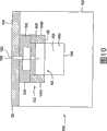
图6描述了用于根据另一实施例的静电夹盘的流体分布元件的横剖视图;6 depicts a cross-sectional view of a fluid distribution element for an electrostatic chuck according to another embodiment;
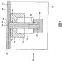
图7描述了根据本发明又一实施例的静电夹盘的流体分布元件的横剖视图;7 depicts a cross-sectional view of a fluid distribution element of an electrostatic chuck according to yet another embodiment of the present invention;
图8描述了根据本发明各种实施例的静电夹盘的流体分布元件的横剖视图;8 depicts a cross-sectional view of a fluid distribution element of an electrostatic chuck according to various embodiments of the invention;
图9描述了根据本发明各种实施例的静电夹盘的流体分布元件的横剖视图;以及9 depicts a cross-sectional view of a fluid distribution element of an electrostatic chuck according to various embodiments of the invention; and
图10描述了根据本发明各种实施例的静电夹盘的流体分布元件的横剖视图。10 depicts a cross-sectional view of a fluid distribution element of an electrostatic chuck according to various embodiments of the invention.
尽管此处使用若干实施例和图示性附图以示例的方式描述了本发明,本领域的一般技术人员将认识到本发明不限于所描述的实施例和附图。应该理解到附图极其详细的描述不意在将本发明限制到所公开的特定形式,而是相反,本发明是要覆盖落在所付的权利要求所限定的本发明的精神和范围内的所有修改、等同物和替换。此处所使用的标题仅仅用于组织目的,并不意味着用来限制描述或者权利要求的范围。对于在整个申请中所使用的,词语“可以”是在允许的意义上使用(即,意思是具有潜在可能性),而不是命令的意义(即,必须的意思)类似地,词语“包括”意思是包括但不限于。Although the invention is described herein by way of example using several embodiments and illustrative drawings, those of ordinary skill in the art will recognize that the invention is not limited to the described embodiments and drawings. It should be understood that the detailed description of the drawings is not intended to limit the invention to the particular form disclosed, but on the contrary, the invention is intended to cover all that fall within the spirit and scope of the invention as defined by the appended claims. Modifications, Equivalents and Substitutions. Headings used herein are for organizational purposes only and are not meant to limit the scope of the description or claims. As used throughout this application, the word "may" is used in the permissive sense (i.e., meaning having the potential to) rather than the imperative sense (i.e., meaning having to). Similarly, the word "comprises" means including but not limited to.
具体实施方式Detailed ways
图1图示了包括根据本发明各种实施例的静电夹盘68的基于等离子体衬底处理系统36。等离子体处理系统36用于在形成和维持处理衬底的等离子体环境的同时对诸如硅晶片、镓砷晶片等的衬底进行温度控制处理。等离子体形成在衬底附近以处理衬底,并且使用各种技术(诸如,通过将传热流体供应到衬底的背面)来控制衬底的温度。尽管在诸如从Santa Clara,Calif的Applied Materials,Inc.购得的300mmHDP-CVD最终X系统的高密度等离子体化学蒸气沉积(HDP-CVD)系统宗图示性地描述等离子体处理室的一个实施例,本发明还可以用在使用等离子体的其它处理室中,包括物理蒸气沉积室、化学蒸气沉积室、蚀刻室和期望对衬底进行温度控制的其它应用中。FIG. 1 illustrates a plasma-based
图1图示了HDP-CVD系统36的一个实施例,其中静电夹盘68用来在处理过程中固定衬底。根据本发明的实施例,静电夹盘68设计成减小夹盘68附近的等离子体穿透和电弧。Figure 1 illustrates one embodiment of an HDP-
系统36包括处理室38、真空系统40、源等离子体系统42、偏置等离子体系统44、气体输送系统46和远程等离子体清洁系统48。
处理室38的上部包括穹顶50,其由诸如铝或者铝氮化物的电介质材料制成。穹顶50限定等离子体处理区域52的上边界。等离子体处理区域52以衬底54的上表面和衬底支撑构件56为底部边界。The upper portion of the
加热板58和冷却板60放在穹顶50上并热耦合到穹顶50。加热板58和冷却板60允许将穹顶温度控制在约+/—10摄氏度,在约100至200摄氏度的范围上。这允许使各种处理的穹顶温度最佳化。例如,可以期望地将穹顶维持用于清洁或者蚀刻处理的温度比用于沉积处理的温度要高。对穹顶温度的精确控制还减小在处理室中薄片或者颗粒,并提高了沉积层和衬底之间的粘附。
处理室38的下部包括本体构件62,其将处理室接合到真空系统。衬底支撑构件56的基部64安装在本体构件62上,并与本体构件62一起形成连续内表面。衬底由机械手叶片(未示出)通过处理室38的一侧中的插入/移除开口95而被转移进入处理室38和从处理室38转移出来。气动致动器(未示出)升高和降低升降销板(未示出),升降销板升高和降低升降销(未示出),升降销升高和降低晶片。在转移进入处理室38中时,衬底被装载到升高的升降销56上,然后降低到衬底支撑构件56的衬底接收部分66。衬底接收部分66包括在衬底处理过程中将衬底固定到衬底支撑构件56的静电夹盘68。The lower portion of the
真空系统40包括节流本体70,节流本体70容纳多叶片节流阀72,并安装到门阀74和涡轮分子泵76。应该注意到,如在共同待审共同转让的美国专利申请、于1995年12月12日原始递交并于1996年9月11日再次递交的转让序号No.08/574,839和题为“SYMMETRIC CHAMBER”的转让序号No.08/712,724中描述,节流本体70提供对气体流动最小阻碍,并允许对称泵送。门阀74能够将泵76从节流本体70隔离,并还能够通过当节流阀72被完全打开时限制排气流量来控制处理室压力。节流阀72、门阀74和涡轮分子泵76的布置允许精确和稳定控制处理室压力从约1至100millitorr。The vacuum system 40 includes a
源等离子体系统42包括安装在穹顶50上的顶部线圈78和侧面线圈80。对称接地屏蔽(未示出)减小线圈之间的电耦合。顶部线圈78由顶部RF源产生器82提供功率,而侧面线圈80由侧面RF源产生器84提供功率,以允许每个线圈独立的功率水平和工作频率。这双线圈系统允许控制处理室38中径向离子密度,由此提高等离子体均匀性。侧面线圈80和顶部线圈78将能量感应地耦合到室38中。在具体的实施例中,顶部RF源产生器82提供通常的2MHz、达8000W的RF功率,并且侧面RF源产生器84提供通常的2MHz、达8000W的RF功率。顶部和侧面RF产生器的工作频率可以从通常的工作频率偏离(例如,分别到1.7-1.9MHz和1.9-2.1MHz)以提高等离子体产生效率。
RF产生器82和84包括数字控制的合成器,并在从约1.7至约2.1MHz的频率范围上工作。每个产生器包括从处理室通过线圈回到产生器的反射功率的RF控制电路(未示出),并调节工作频率以获得最低反射功率,以上这些可以由本领域的一般技术人员理解到。RF产生器通常设计成特征阻抗为50ohms的负载。RF功率可以从具有与产生器不同的特征阻抗的负载反射。这能够减小传输到负载的功率。此外,从负载反射回到产生器的功率会使产生器过载,并损坏产生器。因为等离子体的阻抗的范围可以从小于5ohms到超过900ohms,除了其它因素之外还取决于等离子体离子密度,并且因为反射功率可以是频率的函数,根据反射功率调节产生器频率增大了从RF产生器传输到等离子体的功率,并保护了产生器。减小反射功率并提高效率的另一方式是利用匹配网络。
匹配网络89和90分别将产生器82和84的输出阻抗与线圈78和80匹配。RF控制电路可以通过改变匹配网络内的电容器的值来调谐两个匹配网络以随着负载改变而使产生器匹配到负载。当从负载反射回到产生器的功率超过特定限制时,RF控制电路可以调谐匹配网络。提供恒定的匹配并且有效地使RF控制电路不能调谐匹配网络的一种方式是将反射功率限制设定成超过任何反射功率的预期值。这有助于在一些条件下通过使匹配网络在最近的条件下恒定来稳定等离子体。
偏置等离子体系统44包括RF偏置产生器86和偏置匹配网络88。偏置等离子体系统55将衬底接收部分66电容耦合到本体构件62,衬底接收部分66和本体构件62用作互补电极。偏置等离子体系统44用来提高由源等离子体系统42形成的等离子体物种到衬底的表面的运输。在具体实施例中,RF偏置产生器86提供13.56MHz、达10000W的RF功率。
其它措施还有助于稳定等离子体。例如,RF控制电路能够用来确定输送到负载(等离子体)的功率,并可以在层的沉积过程中增大或者减小产生器输出功率以保持输送的功率大致恒定。Other measures also help stabilize the plasma. For example, RF control circuitry can be used to determine the power delivered to the load (plasma), and the generator output power can be increased or decreased during deposition of the layer to keep the delivered power approximately constant.
气体输送系统46包括多个气体源100a、100b、100c、100d和100e。在一个实施例中,前述气体源分别包括硅烷、分子氧、氦和氩。气体输送系统46提供从多个源到处理室的气体,以经由气体输送线92(仅仅示出了其中一些)处理衬底。气体通过气体环94、顶部喷嘴96和顶部出口98。具体地,气体源100a和100d经由各自的流动控制器120和120c以及气体输送线92将气体提供到顶部喷嘴96。来自气体源100b的气体经由流动控制器120b提供到气体出口98。顶部喷嘴96和顶部出口98允许独立地控制顶部和侧面气体的流动,这提高了膜的均匀性并允许微调节膜的沉积和掺杂的参数。顶部出口98是绕顶部喷嘴96的环形开口,通过该顶部出口98,气体可以从气体输送系统流入处理室中。
气体从每个前述的气体源经由流动控制器102a、102b、102c、102d和102e以及气体输送线92提供到气体环94。气体环94具有多个气体喷嘴106和108(仅仅示出其中的两个),该气体喷嘴在衬底上方提供均匀的气体流动。通过改变气体环94可以改变喷嘴长度和喷嘴角度。这允许为单个处理室内的特定处理修整均匀性的分布和气体利用效率。在具体的实施例中,气体环94具有共计为36的气体喷嘴:24个第一气体喷嘴108和12个第二气体喷嘴106。通常,气体喷嘴108(仅仅示出了其中一个)与第二气体喷嘴106共面,并比第二气体喷嘴106短。Gas is provided to
在一些实施例中,可以使用易燃的、毒性的或者腐蚀性气体。在这些情况下,期望地在沉积之后消除留在气体输送线中的气体。这可以这样来完成:例如使用诸如阀112的三通阀以将处理室38与输送线92a隔离,并将输送线92连通到前级真空管线114。如在图1中所示,诸如112a和112b的其它类似阀可以结合在其它气体输送线上。这种三通阀可以根据实际靠近处理室38布置,以使未连通的气体输送线(在三通阀和处理室之间)的体积最小化。此外,两通(开关)阀(未示出)可以布置在流量控制器(MFC)和处理室之间或者气体源和MFC之间。In some embodiments, flammable, toxic or corrosive gases may be used. In these cases, it is desirable to eliminate the gas left in the gas delivery line after deposition. This can be accomplished by, for example, using a three-way valve such as
系统36还可以包括远程清洁RF等离子体源(未示出),以向室38的顶部喷嘴96提供清洁气体。在其它实施例中,清洁气体(如果使用)可以在其它位置进入室38。
系统控制器132调节系统36的工作,并包括与系统36电连接以调节其操作的处理器134。通常,处理器134是单板计算机(SBC)的一部分,单板计算机包括模拟和数字输入/输出板、接口板和步进电动机控制器板。CVD系统36的各种部件符合Versa Modular European(VME)标准,该标准限定板、插件盒以及连接器类型和尺寸。VME标准还限定总线结构具有16比特数据总线和24比特地址总线。处理器134执行系统控制软件。该系统控制软件是存储在存储器136中的计算机程序,其中存储器136电耦合到处理器134。可以采用任何类型的存储器装置,诸如硬盘驱动器、软盘驱动器、插件板导轨或者它们的组合。系统控制软件包括指令时间、气体混合。处理室压力、处理室温度、微波功率水平、基座位置和特定处理的其它参数的指示组。A
衬底104的温度和衬底温度的均匀性是用于处理衬底104的重要的处理参数。为了产生均匀的温度分布,传热流体涂在夹盘68和衬底104的背面之间。例如,本发明的一个实施例使用氦作为传热流体。一般地,静电夹盘68的形状为圆形,但是可选地,静电夹盘68可以包括各种规则和不规则几何形状,以容纳非圆形衬底(例如,方形或者矩形衬底,诸如平板)。The temperature of the
在工作中,衬底104被放在静电夹盘68上,并且多个气态成分从气体面板46供应到等离子处理室38的处理区域52以形成气态混合气。为了点燃等离子体,RF功率施加到衬底支撑构件56中的一个或者多个电极、顶部线圈78或者侧面线圈80。为了在处理过程中维持衬底的温度的均匀性,根据本发明的实施例经由至少一个流体分布元件(以下示出并论述)供应诸如氦气的传热流体。In operation,
图2图示了根据本发明一个实施例的具有流体分布元件222的静电夹盘68的顶平面视图。图2A描述了图2的静电夹盘68的局部剖视立体视图。图3描述了图2的夹盘68沿着线3-3所取的横剖视图。通过同时参照图2和图3可以最佳理解以下公开的内容。静电夹盘68包括本体220、流体分布元件222和电介质层224。在静电夹盘68的一个实施例中,本体220由诸如铝的导电材料制成,并且电介质层224是诸如铝氮化物、氧化铝等的陶瓷材料。流体分布元件222以圆周的方式布置在静电夹盘68的周边附近。流体分布元件222包括多个孔230(或者其它形式的通路),其穿过电介质层224以将诸如氦气的流体从静电夹盘分布到衬底的背面。对于与12inch(300mm)直径半导体晶片组合使用的静电夹盘102,在静电夹盘102的周边周围在60个孔和360个孔之间。每个多个孔230通常波动约0.15mm直径。取决于所使用的流体分布元件的种类,在处理室内所使用的压力和通过流体分布元件222的气体流量来调节这些尺寸。FIG. 2 illustrates a top plan view of an
流体分布元件222具有环形结构。然而,在可选实施例中,流体分布元件222可以根据处理方法和用户需要具有各种几何形状设计,并包括多个环、径向臂、辐板和环的组合等。本发明的实施例不限制流体分布元件的几何形状。The
电介质层224覆盖本体220的顶面的至少一部分和流体分布元件222的至少一部分,由此形成支撑表面228。支撑表面228支撑放在其上的衬底104。电介质层224可以喷涂到本体的顶面上并抛光到期望的厚度。
本体220包括顶表面332和形成到本体220的顶表面332中的通道334。一般,通道334具有矩形横剖形状。然而,在可选实施例中,通道334可以具有各种几何横剖形状。流体分布元件222耦合到本体220,使得通道334和流体分布元件222形成充气空间336,即,元件222定位到通道334中并固定到通道334。此外,本体220包括连接到通道334的导管338,以将流体提供到充气空间336。根据本发明一个实施例,冷却气体可以通过导管338供应,并被充气空间分布到流体分布元件222。气体通过一个或者多个多个孔230(或者其它形式的通路)流出,由此,将传热介质供应到衬底的背面。
图4至图10图示了静电夹盘(例如,静电夹盘102)的虚线部分230的横剖视图,该部分具有流体分布元件222、电介质层228和本体220。在图示中,静电夹盘的尺寸已经被放大以图示流体分布元件和本体的横剖面。4-10 illustrate cross-sectional views of a dashed-
具体地,图4示出了根据本发明一个实施例的静电夹盘402的一部分。本体220包括具有下通道404A和上通道404B的双镶嵌通道404,其中下通道404A比上通道404B窄。静电夹盘402包括流体分布元件442,该流体分布元件442包括板4490和电介质管442。板440装配到上通道404B中(例如,板具有圆形平面形式以匹配通道404),使得上通道404B的基部406形成挡块。板440的高度与上通道404B的高度大致相同,使得板440的顶部408与本体220的顶部332大致共面。板440可以由诸如铝的导电材料制成,并焊接到上通道404B的位置中。板440还包括在板440的底面中形成的通道410。在本发明的一个实施例中,通道440的宽度大致类似于下通道404A的宽度;然而,在其它实施例中,通道410可以具有比通道404A窄的宽度。下通道404A和通道410组合限定充气空间336。Specifically, FIG. 4 illustrates a portion of an
电介质管442(电绝缘体)包括第一端446、第二端448和轴向通孔450。例如,由氧化铝制成的电介质管442具有的直径大致匹配板440中开口444的直径。开口444的直径一般但不受限制地为约0.008inches(约0.2mm)或者更大。在可选实施例中,开口444可以具有各种几何形状,诸如圆形、矩形、方形等。此外,开口的形状和尺寸大致匹配电介质管442的形状和外径的尺寸。电介质管442定位(例如压配合)到开口444中。开口444包括凸缘412,管子442靠在凸缘412上(例如,凸缘形成挡块)。在所描述的实施例中,管子442的第一端446在本体220的表面332的上方延伸。在其它实施例中,管子442的第一端446可以与表面332共面。The dielectric tube 442 (electrical insulator) includes a
本体220的至少一部分和流体分布元件422的至少一部分由电介质层224覆盖,由此形成支撑表面428。电介质层224可以喷涂到本体的顶表面上,并被抛光到期望的厚度。在一个实施例中,电介质层224包括热喷涂氧化铝或者喷涂氧化铝/氧化钛。用于此热喷涂电介质层的应用的处理是现有技术中公知的。热喷涂处理能够从若干不同方法(诸如,等离子体喷涂、爆炸喷涂、高速氧燃料(HVOF)喷涂和框架喷涂)选择。At least a portion of
在一个实施例中,电介质层224被抛光到由线414所表示的厚度,使得层224的表面428与管子442的一端446共面。可选地,电介质层224可以是多孔陶瓷,使得层224被抛光到特定的平面度,但是层224至少覆盖管子442的第一端446。由于陶瓷的孔隙率,来自充气空间的气体流经管子442和电介质层224。例如,靠近管子442的第一端446的电介质层224可以整个或者部分地由氧化铝形成,且孔隙率在10和60体积百分比之间,这将导致孔的直径在约1至100um。在一些实施例中,如以下参照图8所描述,电介质层可以在靠近管子442的一端446处多孔,并在其它位置孔较少。如所图示,通路445有利地缺少从支撑表面428到充气空间436的直接视线路径,由此限制在通路445中形成等离子体的可能。在另一实施例中,在层224覆盖管子442的第一端446的情况下电介质层224被抛光到特定的平面度。孔416能够被镗孔或者以其它方式形成(例如,激光钻孔)穿过电介质层416到通路445中。镗孔处理仅仅镗孔穿过电介质材料,即,本体的导电材料不被镗孔处理溅射。In one embodiment,
如在现有技术中所公知,支撑表面428还被处理以提供在电介质层224上形成的槽的图案(在附图中未示出)。槽被机械加工或者以其它方式形成到支撑表面428中,使得它们与通路445相交。冷却气体从通路445行进进入槽中,以将冷却气体均匀地分布在静电夹盘402的整个支撑表面马428上。
通过使用电绝缘体(电介质管和/或者电介质层)以限定充气空间和衬底表面之间的通路,减小了从传热气体形成等离子体或者由于等离子体形成的电弧的潜在可能性。通过减小或者消除等离子体形成和电弧,静电夹盘的寿命得到显著增加。绝缘体的使用减小了通路中的电场;因而,减小了等离子体形成的机会。此外,本发明的某些实施例利用流体分布元件结构以通过消除衬底支撑表面(存在高电场之处)和充气空间的导电表面的视线路径来进一步减小电场。当这种视线路径存在时,通路中的流体体积足以被点燃进入到等离子体中。使用非视线路径减小了在足够大体积的流体上建立的电场(该电场会导致等离子体形成)。这样,等离子体形成和相关的电弧被减小或者消除。By using electrical insulators (dielectric tubes and/or dielectric layers) to define the passage between the plenum space and the substrate surface, the potential for plasma formation from the heat transfer gas or arcing due to the plasma is reduced. By reducing or eliminating plasma formation and arcing, the lifetime of the electrostatic chuck is significantly increased. The use of an insulator reduces the electric field in the pathway; thus, the chance of plasma formation is reduced. In addition, certain embodiments of the present invention utilize fluid distribution element structures to further reduce electric fields by eliminating line-of-sight paths from substrate support surfaces (where high electric fields exist) and conductive surfaces of the plenum space. When such a line-of-sight path exists, the volume of fluid in the passage is sufficient to be ignited into the plasma. Using a non-line-of-sight path reduces the electric field that would build up across a sufficiently large volume of fluid that would lead to plasma formation. In this way, plasma formation and associated arcing is reduced or eliminated.
图5图示了根据本发明另一实施例的静电夹盘502的一部分的横剖面。类似于图4的实施例,电介质管542穿过板400定位。在此可选的实施例中,管子542延伸到通道534的管子542的第二端548靠在形成在通道534的底部中的支撑元件(例如台阶556)上的底部。如在之前的实施例中,电介质管542和/或者电介质层224的一部分形成限定用于从充气空间536到表面528的流体的通道545的电绝缘体。FIG. 5 illustrates a cross-section of a portion of an
图6图示了根据本发明另一实施例的静电夹盘602的一部分的横剖面。类似于图4和图5的实施例,电介质管642穿过板440定位。在此可选的实施例中,电介质管642包括至少一个在第二端604中形成的切口656。在可选实施例中,管子642可以包括孔以流体从充气空间636流动到管子642中的通道645。如之前实施例那样,电介质层224可以多孔,并覆盖管子642的第一端606,层224可以被抛光以露出管子642的第一端606,或者露出在层中形成的孔以接近通道645。电介质管642和电介质层224的一部分形成用于来自充气空间636的流体的通道645。如所图示,当电介质层224是多孔,并覆盖管子642时,通道645有利地缺少从支撑表面628到充气空间636的直接视线路径,由此限制在通道645中形成等离子体。FIG. 6 illustrates a cross-section of a portion of an electrostatic chuck 602 according to another embodiment of the invention. Similar to the embodiment of FIGS. 4 and 5 , a dielectric tube 642 is positioned through the
图7图示根据本发明又一实施例的静电夹盘702的一部分的横剖面。静电夹盘702包括本体720和流体分布元件722。流体分布元件722包括以与之前实施例相同方式组装的板740和电介质管742。在此实施例中,本体720包括通道734,该通道734包括电介质端帽760。电介质端帽760定位在通道734的底部。电介质端帽760包括开口762,使得帽子760呈杯形。电介质管742包括第一端746、第二端748和连接第一端746和第二端748的轴向通孔750。在本发明的一个实施例中,电介质层724覆盖管子742的第一端746,并且在第二实施例中,电介质层724被抛光到线414,以露出管子742的第一端746。电介质帽746定位到通道734中,使得管子742的第二端748延伸进入开口762中,但与开口762间隔开,以形成间隙。管子742和端帽760形成流体流经的迷宫式通道。使用此通道确保了从导电充气空间壁到夹盘表面的视线路径不存在。FIG. 7 illustrates a cross-section of a portion of an
图8图示了根据本发明另一实施例的静电夹盘802的一部分的横剖图。静电夹盘802包括流体分布元件822。流体分布元件822包括板840,板840包括开口844。板840耦合到本体820,使得通道834和板840形成充气空间836。电介质层824覆盖本体820至少一部分和流体分布元件822的至少一部分。电介质层824包括多孔电介质部分870,使得多孔电介质部分870的至少一部分与开口844重叠。多孔电介质部分870是具有互连的开口的多孔陶瓷,诸如孔隙率的范围从约10体积百分比到约60体积百分比的氧化铝,互连的开口形成穿过多孔电介质部分870的连续的过道。开口844和多孔电介质部分870的至少一部分形成用于流体从充气空间836流动道静电夹盘802的支撑表面828的通路845。如所图示,通路845有利地缺少从支撑表面828到导电充气空间836的直接视线路径,由此禁止等离子体形成到通路845中。FIG. 8 illustrates a cross-sectional view of a portion of an
图9图示了根据本发明另一实施例的静电夹盘902的一部分的横剖面。静电夹盘902包括流体分布元件922。流体分布元件922包括具有开口944的板940和电介质塞980。板940耦合到本体920,使得通道934和板940形成充气空间936。板940和本体920如以上所述的本发明其它实施例那样组装。电介质塞980的直径大致与开口944的直径匹配。电介质塞980定位在开口1044中,并通常压配在其中。电介质层224覆盖本体920的至少一部分和流体分布元件922的至少一部分,由此形成支撑表面928。电介质层224可以喷涂到本体920和流体分布元件922的顶表面上,并被抛光到期望的厚度。孔982形成穿过电介质层224并穿过电介质塞980。孔982使得流体能够从充气空间936流到静电夹盘902的支撑表面928。可以使用诸如机械钻孔、激光钻孔等的各种技术形成孔982。孔982被形成仅仅穿过电介质材料。这样,没有从钻孔处理残余的材料能够形成在轴向通孔982上。没有金属残余,就限制了孔982中的等离子体形成或者电弧的可能性。FIG. 9 illustrates a cross-section of a portion of an electrostatic chuck 902 according to another embodiment of the invention. Electrostatic chuck 902 includes fluid distribution element 922 . Fluid distribution element 922 includes a plate 940 having openings 944 and a dielectric plug 980 . Plate 940 is coupled to body 920 such that channel 934 and plate 940 form plenum 936 . Plate 940 and body 920 are assembled as described above for other embodiments of the invention. The diameter of the dielectric plug 980 generally matches the diameter of the opening 944 . Dielectric plug 980 is positioned in opening 1044 and is typically press fit therein.
图10图示了根据本发明另一实施例的静电夹盘1002的一部分的横剖面。静电夹盘1002包括流体分布元件1022。流体分布元件1022包括板1040和电介质帽1042。板1040包括两个圆形环1040A和1040B。环1040A具有比环1040B小的直径。每个环1040A和1040B靠在形成在上通道4040B的底部处的凸缘406上。板1040被焊接到本体1020以将板保持在上通道404B中。电介质帽1042(成环形以形成充气空间1036)插入到上通道404B中,并靠在板1040上。FIG. 10 illustrates a cross-section of a portion of an
在另一实施例中,板1040可以包括倒U形横剖面(例如,图4的板440),并具有多个埋头孔。横剖面类似于元件1042的圆形(圆圈形)电介质元件可以插入该埋头孔中。流体分布元件1022耦合到本体1020,使得流体分布元件1022和通道1034形成充气空间1036。电介质层覆盖本体1020的至少一部分和流体分布元件1022的至少一部分,由此形成支撑表面1028。电介质层224可以喷涂到本体1020和流体分布元件1022的顶表面上,并被抛光到期望的厚度。孔1082穿过电介质层224和电介质帽1090而形成。可以使用诸如机械加工、激光加工等各种技术对孔1082进行钻孔。如图9的实施例那样,孔1082仅仅穿过电介质材料形成。这样,没有导电残余物留在孔1082中。In another embodiment,
在前述实施例的每个中,在利用本发明的流体分布元件的静电夹盘被等离子体的形成或者电弧损坏的情况不可能发生,因而能够使用一些方法容易地对夹盘进行修理(或者重新修整)。一般地,在靠近电介质部件(管子、多孔插件等)处或者在其内将发生有损坏性的等离子体形成或者电弧。这样,电介质层可以局部地(在电介质部件上)或者整体地(在整个夹盘上)被移除以露出电介质元件。然后,使用拔出工具以将该部件钻孔取出或者拉出来移除该部件。一旦被移除,新的电介质部件能够被插入,并根据需要局部地或者整体地更换电介质层。在一些实施例中,电介质部件可以延伸到夹盘的支撑表面(如以上所述),并且在拔出之前不需要移除电介质层。在这情况下,受损的电介质部件被移除,新的电介质部件插入(一般压配合)到板中的开口中。以此方式,与在电弧或者等离子体形成时在传热流体通路中或者附近更换整个静电夹盘相比,能够以显著的节约费用对静电夹盘进行修理。In each of the foregoing embodiments, it is unlikely that the electrostatic chuck utilizing the fluid distribution element of the present invention will be damaged by plasma formation or arcing, so that the chuck can be easily repaired (or re-installed) using some method. trimming). Typically, damaging plasma formation or arcing will occur close to or within dielectric components (tubes, porous inserts, etc.). In this way, the dielectric layer can be removed locally (on the dielectric part) or entirely (on the entire chuck) to expose the dielectric element. An extraction tool is then used to drill or pull out the part to remove the part. Once removed, new dielectric components can be inserted and the dielectric layer replaced partially or entirely as needed. In some embodiments, the dielectric member may extend to the support surface of the chuck (as described above), and the dielectric layer need not be removed prior to extraction. In this case, the damaged dielectric part is removed and a new dielectric part is inserted (typically press fit) into the opening in the board. In this manner, the electrostatic chuck can be repaired at significant cost savings compared to replacing the entire electrostatic chuck in or near the heat transfer fluid path when an arc or plasma is formed.
尽管前述涉及本发明的实施例,但是在不脱离由权利要求所确定的范围的情况下可以设计本发明其它和另外的实施例。While the foregoing relates to embodiments of the invention, other and further embodiments of the invention may be devised without departing from the scope defined by the claims.
Claims (25)
Applications Claiming Priority (6)
| Application Number | Priority Date | Filing Date | Title |
|---|---|---|---|
| US11/888,327 | 2007-07-31 | ||
| US11/888,341 | 2007-07-31 | ||
| US11/888,311 | 2007-07-31 | ||
| US11/888,341US9202736B2 (en) | 2007-07-31 | 2007-07-31 | Method for refurbishing an electrostatic chuck with reduced plasma penetration and arcing |
| US11/888,311US7848076B2 (en) | 2007-07-31 | 2007-07-31 | Method and apparatus for providing an electrostatic chuck with reduced plasma penetration and arcing |
| US11/888,327US8108981B2 (en) | 2007-07-31 | 2007-07-31 | Method of making an electrostatic chuck with reduced plasma penetration and arcing |
Publications (2)
| Publication Number | Publication Date |
|---|---|
| CN101425474Atrue CN101425474A (en) | 2009-05-06 |
| CN101425474B CN101425474B (en) | 2011-05-25 |
Family
ID=40337867
Family Applications (1)
| Application Number | Title | Priority Date | Filing Date |
|---|---|---|---|
| CN2008101349160AExpired - Fee RelatedCN101425474B (en) | 2007-07-31 | 2008-07-31 | Methods and apparatus for providing an electrostatic chuck that reduces plasma breakthrough and arcing |
Country Status (2)
| Country | Link |
|---|---|
| US (1) | US7848076B2 (en) |
| CN (1) | CN101425474B (en) |
Cited By (3)
| Publication number | Priority date | Publication date | Assignee | Title |
|---|---|---|---|---|
| CN108359957A (en)* | 2010-10-29 | 2018-08-03 | 应用材料公司 | Deposition ring and electrostatic chuck for physical vapor deposition chamber |
| CN112687602A (en)* | 2019-10-18 | 2021-04-20 | 中微半导体设备(上海)股份有限公司 | Electrostatic chuck, manufacturing method thereof and plasma processing device |
| CN112908919A (en)* | 2019-12-04 | 2021-06-04 | 中微半导体设备(上海)股份有限公司 | Electrostatic chuck device and plasma processing device comprising same |
Families Citing this family (34)
| Publication number | Priority date | Publication date | Assignee | Title |
|---|---|---|---|---|
| JP5635001B2 (en)* | 2008-09-26 | 2014-12-03 | ラム リサーチ コーポレーションLam Research Corporation | Thermal contact between electrostatic chuck and hot edge ring adjustable by clocking the coupling ring |
| US9218997B2 (en)* | 2008-11-06 | 2015-12-22 | Applied Materials, Inc. | Electrostatic chuck having reduced arcing |
| US9728429B2 (en) | 2010-07-27 | 2017-08-08 | Lam Research Corporation | Parasitic plasma prevention in plasma processing chambers |
| US8968537B2 (en) | 2011-02-09 | 2015-03-03 | Applied Materials, Inc. | PVD sputtering target with a protected backing plate |
| US9034199B2 (en) | 2012-02-21 | 2015-05-19 | Applied Materials, Inc. | Ceramic article with reduced surface defect density and process for producing a ceramic article |
| US9212099B2 (en) | 2012-02-22 | 2015-12-15 | Applied Materials, Inc. | Heat treated ceramic substrate having ceramic coating and heat treatment for coated ceramics |
| US9090046B2 (en) | 2012-04-16 | 2015-07-28 | Applied Materials, Inc. | Ceramic coated article and process for applying ceramic coating |
| US9604249B2 (en) | 2012-07-26 | 2017-03-28 | Applied Materials, Inc. | Innovative top-coat approach for advanced device on-wafer particle performance |
| US9343289B2 (en) | 2012-07-27 | 2016-05-17 | Applied Materials, Inc. | Chemistry compatible coating material for advanced device on-wafer particle performance |
| US9916998B2 (en) | 2012-12-04 | 2018-03-13 | Applied Materials, Inc. | Substrate support assembly having a plasma resistant protective layer |
| US9685356B2 (en) | 2012-12-11 | 2017-06-20 | Applied Materials, Inc. | Substrate support assembly having metal bonded protective layer |
| US8941969B2 (en) | 2012-12-21 | 2015-01-27 | Applied Materials, Inc. | Single-body electrostatic chuck |
| US9358702B2 (en) | 2013-01-18 | 2016-06-07 | Applied Materials, Inc. | Temperature management of aluminium nitride electrostatic chuck |
| US9669653B2 (en) | 2013-03-14 | 2017-06-06 | Applied Materials, Inc. | Electrostatic chuck refurbishment |
| US9887121B2 (en) | 2013-04-26 | 2018-02-06 | Applied Materials, Inc. | Protective cover for electrostatic chuck |
| US9666466B2 (en) | 2013-05-07 | 2017-05-30 | Applied Materials, Inc. | Electrostatic chuck having thermally isolated zones with minimal crosstalk |
| US9865434B2 (en) | 2013-06-05 | 2018-01-09 | Applied Materials, Inc. | Rare-earth oxide based erosion resistant coatings for semiconductor application |
| US9850568B2 (en) | 2013-06-20 | 2017-12-26 | Applied Materials, Inc. | Plasma erosion resistant rare-earth oxide based thin film coatings |
| US9966240B2 (en) | 2014-10-14 | 2018-05-08 | Applied Materials, Inc. | Systems and methods for internal surface conditioning assessment in plasma processing equipment |
| US9355922B2 (en) | 2014-10-14 | 2016-05-31 | Applied Materials, Inc. | Systems and methods for internal surface conditioning in plasma processing equipment |
| US10224210B2 (en) | 2014-12-09 | 2019-03-05 | Applied Materials, Inc. | Plasma processing system with direct outlet toroidal plasma source |
| US10573496B2 (en) | 2014-12-09 | 2020-02-25 | Applied Materials, Inc. | Direct outlet toroidal plasma source |
| US9728437B2 (en) | 2015-02-03 | 2017-08-08 | Applied Materials, Inc. | High temperature chuck for plasma processing systems |
| US9999947B2 (en)* | 2015-05-01 | 2018-06-19 | Component Re-Engineering Company, Inc. | Method for repairing heaters and chucks used in semiconductor processing |
| US9691645B2 (en) | 2015-08-06 | 2017-06-27 | Applied Materials, Inc. | Bolted wafer chuck thermal management systems and methods for wafer processing systems |
| US9741593B2 (en) | 2015-08-06 | 2017-08-22 | Applied Materials, Inc. | Thermal management systems and methods for wafer processing systems |
| US10504700B2 (en) | 2015-08-27 | 2019-12-10 | Applied Materials, Inc. | Plasma etching systems and methods with secondary plasma injection |
| US10020218B2 (en) | 2015-11-17 | 2018-07-10 | Applied Materials, Inc. | Substrate support assembly with deposited surface features |
| US11047035B2 (en) | 2018-02-23 | 2021-06-29 | Applied Materials, Inc. | Protective yttria coating for semiconductor equipment parts |
| US11694879B2 (en)* | 2018-12-07 | 2023-07-04 | Applied Materials, Inc. | Component, method of manufacturing the component, and method of cleaning the component |
| US12300473B2 (en)* | 2019-03-08 | 2025-05-13 | Applied Materials, Inc. | Electrostatic chuck for high bias radio frequency (RF) power application in a plasma processing chamber |
| US12165897B2 (en)* | 2019-11-25 | 2024-12-10 | Kyocera Corporation | Workpiece holding tool |
| US12341048B2 (en) | 2021-11-29 | 2025-06-24 | Applied Materials, Inc. | Porous plug for electrostatic chuck gas delivery |
| JP7356620B1 (en) | 2022-08-12 | 2023-10-04 | 日本碍子株式会社 | Components for semiconductor manufacturing equipment |
Family Cites Families (15)
| Publication number | Priority date | Publication date | Assignee | Title |
|---|---|---|---|---|
| US5883778A (en)* | 1994-02-28 | 1999-03-16 | Applied Materials, Inc. | Electrostatic chuck with fluid flow regulator |
| US5644467A (en)* | 1995-09-28 | 1997-07-01 | Applied Materials, Inc. | Method and structure for improving gas breakdown resistance and reducing the potential of arcing in a electrostatic chuck |
| US5720818A (en)* | 1996-04-26 | 1998-02-24 | Applied Materials, Inc. | Conduits for flow of heat transfer fluid to the surface of an electrostatic chuck |
| US6108189A (en)* | 1996-04-26 | 2000-08-22 | Applied Materials, Inc. | Electrostatic chuck having improved gas conduits |
| US6572814B2 (en)* | 1998-09-08 | 2003-06-03 | Applied Materials Inc. | Method of fabricating a semiconductor wafer support chuck apparatus having small diameter gas distribution ports for distributing a heat transfer gas |
| US6639783B1 (en)* | 1998-09-08 | 2003-10-28 | Applied Materials, Inc. | Multi-layer ceramic electrostatic chuck with integrated channel |
| US6263829B1 (en)* | 1999-01-22 | 2001-07-24 | Applied Materials, Inc. | Process chamber having improved gas distributor and method of manufacture |
| US6310755B1 (en)* | 1999-05-07 | 2001-10-30 | Applied Materials, Inc. | Electrostatic chuck having gas cavity and method |
| US6500299B1 (en)* | 1999-07-22 | 2002-12-31 | Applied Materials Inc. | Chamber having improved gas feed-through and method |
| US6370006B1 (en)* | 2000-02-17 | 2002-04-09 | Applied Materials, Inc. | Electrostatic chuck having a plurality of gas inlet channels |
| US6606234B1 (en)* | 2000-09-05 | 2003-08-12 | Saint-Gobain Ceramics & Plastics, Inc. | Electrostatic chuck and method for forming an electrostatic chuck having porous regions for fluid flow |
| US6581275B2 (en)* | 2001-01-22 | 2003-06-24 | Applied Materials Inc. | Fabricating an electrostatic chuck having plasma resistant gas conduits |
| US6490145B1 (en)* | 2001-07-18 | 2002-12-03 | Applied Materials, Inc. | Substrate support pedestal |
| KR100457833B1 (en)* | 2002-05-24 | 2004-11-18 | 주성엔지니어링(주) | Plasma Etching Apparatus |
| KR100505035B1 (en)* | 2003-11-17 | 2005-07-29 | 삼성전자주식회사 | Electrostatic chuck for supporting a substrate |
- 2007
- 2007-07-31USUS11/888,311patent/US7848076B2/enactiveActive
- 2008
- 2008-07-31CNCN2008101349160Apatent/CN101425474B/ennot_activeExpired - Fee Related
Cited By (3)
| Publication number | Priority date | Publication date | Assignee | Title |
|---|---|---|---|---|
| CN108359957A (en)* | 2010-10-29 | 2018-08-03 | 应用材料公司 | Deposition ring and electrostatic chuck for physical vapor deposition chamber |
| CN112687602A (en)* | 2019-10-18 | 2021-04-20 | 中微半导体设备(上海)股份有限公司 | Electrostatic chuck, manufacturing method thereof and plasma processing device |
| CN112908919A (en)* | 2019-12-04 | 2021-06-04 | 中微半导体设备(上海)股份有限公司 | Electrostatic chuck device and plasma processing device comprising same |
Also Published As
| Publication number | Publication date |
|---|---|
| CN101425474B (en) | 2011-05-25 |
| US20090034147A1 (en) | 2009-02-05 |
| US7848076B2 (en) | 2010-12-07 |
Similar Documents
| Publication | Publication Date | Title |
|---|---|---|
| CN101425474A (en) | Method and apparatus for providing an electrostatic chuck with reduced plasma penetration and arcing | |
| KR101025232B1 (en) | Electrostatic chuck with reduced arcing | |
| US8108981B2 (en) | Method of making an electrostatic chuck with reduced plasma penetration and arcing | |
| US9202736B2 (en) | Method for refurbishing an electrostatic chuck with reduced plasma penetration and arcing | |
| JP7169319B2 (en) | High power electrostatic chuck with aperture reduction plugs in gas holes | |
| US20240112893A1 (en) | Multi-plate electrostatic chucks with ceramic baseplates | |
| TWI810138B (en) | Moveable edge ring designs | |
| KR101125885B1 (en) | Method and apparatus for providing an electrostatic chuck with reduced plasma penetration and arcing | |
| KR102454532B1 (en) | Electrostatic chuck with features for preventing electrical arcing and light-up and improving process uniformity | |
| CN110383454B (en) | Bottom edge ring and middle edge ring | |
| KR102521717B1 (en) | Helium plug design to reduce arcing | |
| WO2024186529A1 (en) | Arc-resistant electrostatic chucks and arc-reducing plugs for electrostatic chucks |
Legal Events
| Date | Code | Title | Description |
|---|---|---|---|
| C06 | Publication | ||
| PB01 | Publication | ||
| C10 | Entry into substantive examination | ||
| SE01 | Entry into force of request for substantive examination | ||
| C14 | Grant of patent or utility model | ||
| GR01 | Patent grant | ||
| CF01 | Termination of patent right due to non-payment of annual fee | Granted publication date:20110525 Termination date:20150731 | |
| EXPY | Termination of patent right or utility model |