CN101421797B - Non-volatile memory and method with redundancy data buffered in remote buffer circuits - Google Patents
Non-volatile memory and method with redundancy data buffered in remote buffer circuitsDownload PDFInfo
- Publication number
- CN101421797B CN101421797BCN2007800135346ACN200780013534ACN101421797BCN 101421797 BCN101421797 BCN 101421797BCN 2007800135346 ACN2007800135346 ACN 2007800135346ACN 200780013534 ACN200780013534 ACN 200780013534ACN 101421797 BCN101421797 BCN 101421797B
- Authority
- CN
- China
- Prior art keywords
- data
- redundant
- column
- array
- memory
- Prior art date
- Legal status (The legal status is an assumption and is not a legal conclusion. Google has not performed a legal analysis and makes no representation as to the accuracy of the status listed.)
- Expired - Fee Related
Links
- 230000015654memoryEffects0.000titleclaimsabstractdescription125
- 239000000872bufferSubstances0.000titleclaimsabstractdescription92
- 238000000034methodMethods0.000titleclaimsdescription23
- 230000002950deficientEffects0.000claimsabstractdescription92
- 238000012546transferMethods0.000claimsdescription28
- 238000013507mappingMethods0.000claimsdescription11
- 230000004044responseEffects0.000claims4
- 230000003139buffering effectEffects0.000claims2
- 230000008878couplingEffects0.000claims1
- 238000010168coupling processMethods0.000claims1
- 238000005859coupling reactionMethods0.000claims1
- 230000007547defectEffects0.000description43
- 238000010586diagramMethods0.000description18
- 238000004519manufacturing processMethods0.000description4
- 238000002955isolationMethods0.000description3
- 238000013459approachMethods0.000description2
- 238000003491arrayMethods0.000description2
- 238000012856packingMethods0.000description2
- 239000004065semiconductorSubstances0.000description2
- 230000002457bidirectional effectEffects0.000description1
- 238000012937correctionMethods0.000description1
- 238000013479data entryMethods0.000description1
- 230000002093peripheral effectEffects0.000description1
- 238000012545processingMethods0.000description1
- 238000003672processing methodMethods0.000description1
- 238000012360testing methodMethods0.000description1
Images


Classifications
- G—PHYSICS
- G11—INFORMATION STORAGE
- G11C—STATIC STORES
- G11C29/00—Checking stores for correct operation ; Subsequent repair; Testing stores during standby or offline operation
- G11C29/70—Masking faults in memories by using spares or by reconfiguring
- G11C29/78—Masking faults in memories by using spares or by reconfiguring using programmable devices
- G11C29/84—Masking faults in memories by using spares or by reconfiguring using programmable devices with improved access time or stability
- G11C29/848—Masking faults in memories by using spares or by reconfiguring using programmable devices with improved access time or stability by adjacent switching
- G—PHYSICS
- G11—INFORMATION STORAGE
- G11C—STATIC STORES
- G11C2229/00—Indexing scheme relating to checking stores for correct operation, subsequent repair or testing stores during standby or offline operation
- G11C2229/70—Indexing scheme relating to G11C29/70, for implementation aspects of redundancy repair
- G11C2229/72—Location of redundancy information
- G11C2229/723—Redundancy information stored in a part of the memory core to be repaired
Landscapes
- For Increasing The Reliability Of Semiconductor Memories (AREA)
- Read Only Memory (AREA)
Abstract
Description
Translated fromChinese技术领域technical field
本发明通常涉及非易失性半导体存储器,例如电可抹除可编程只读存储器(EEPROM)与快闪EEPROM,且具体而言涉及实施列冗余特征的非易失性半导体存储器。 The present invention relates generally to non-volatile semiconductor memories, such as electrically erasable programmable read-only memories (EEPROMs) and flash EEPROMs, and more particularly to non-volatile semiconductor memories implementing row redundancy features. the
背景技术Background technique
能够非易失性存储电荷的固态存储器(特别是采用包装成小形状因数卡的EEPROM及快闪EEPROM的形式)近年来已经成为各种移动及手持装置(尤其是信息器具与消费性电子产品)中选用的存储装置。与同为固态存储器的RAM(随机存取存储器)不同的是,快闪存储器是非易失性的且在关闭电源后保留其已存储的数据。虽然与磁盘存储装置相比成本较高,但快闪存储器越来越多地用于大容量存储应用。常规的大容量存储装置(基于旋转磁性媒体,例如硬驱动和软盘)并不适用于移动及手持环境。这是因为磁盘驱动的体积趋于庞大,容易产生机械故障,而且具有较高的延迟时间以及较高的功率要求。所述不需要的属性使得基于磁盘的存储装置无法在大多数移动式及便携式应用中得到实用。另一方面,快闪存储器(不论是嵌入式或采用可拆卸卡形式)因为其小尺寸、低功率消耗、高速度以及较高可靠性特征而理想地适用于移动及手持环境。 Solid-state memory capable of non-volatile storage of charge, especially in the form of EEPROM and flash EEPROM packaged in small form-factor cards, has in recent years become a popular choice in a variety of mobile and handheld devices, especially information appliances and consumer electronics. The selected storage device. Unlike RAM (random access memory), which is also solid-state memory, flash memory is non-volatile and retains its stored data after the power is turned off. Although costly compared to magnetic disk storage devices, flash memory is increasingly used in mass storage applications. Conventional mass storage devices (based on rotating magnetic media such as hard drives and floppy disks) are not suitable for mobile and handheld environments. This is because disk drives tend to be bulky, prone to mechanical failure, have high latency, and have high power requirements. These undesirable properties make disk-based storage impractical for most mobile and portable applications. On the other hand, flash memory (whether embedded or in the form of a removable card) is ideal for mobile and handheld environments because of its small size, low power consumption, high speed, and high reliability features. the
所述存储器装置一般包含可被安装在卡上的一或一个以上存储器芯片。每一存储器芯片皆包含受周边电路(例如解码器及抹除电路、写入电路以及读取电路)支持的存储器单元阵列。更复杂的存储器装置还会搭配实施智能与更高级存储器操作与介接的控制器。现今正在使用许多市售成功的非易失性固态存储器装置。所述存储器装置可利用不同类型的存储器单元,每一类型具有一个或一个以上电荷存储元件。EEPROM的实例和制造所述EEPROM的方法在美国专利第5,595,924号中给出。快闪EEPROM的实例、其在存储器系统中的使用和制造所述快闪EEPROM的方法在第5,070,032、5,095,344、5,315,541、5,343,063、5,661,053、5,313,421和6,222,762号美国专利中给出。具有NAND单元结构的存储器装置的实例在第5,570,315、5,903,495和6,046,935号美国专利中进行了描述。具有用于存储电荷的介电层的存储器装置的实例由艾坦(Eitan)等人的“规范:新型局部化陷阱、2位非易失性存储器单元(NORM:A NovelLocalized Trapping,2-Bit Nonvolatile Memory Cell)”(2000年11月第11期IEEE电 子装置学报,第21卷,第543-545页)且在第5,768,192和6,011,725号美国专利中进行描述。 The memory device generally includes one or more memory chips that may be mounted on a card. Each memory chip includes an array of memory cells supported by peripheral circuits such as decoder and erase circuits, write circuits, and read circuits. More complex memory devices are also paired with controllers that implement intelligent and more advanced memory operations and interfacing. There are many commercially successful non-volatile solid-state memory devices in use today. The memory device can utilize different types of memory cells, each type having one or more charge storage elements. Examples of EEPROMs and methods of making them are given in US Patent No. 5,595,924. Examples of flash EEPROMs, their use in memory systems, and methods of making them are given in US Patent Nos. 5,070,032, 5,095,344, 5,315,541, 5,343,063, 5,661,053, 5,313,421, and 6,222,762. Examples of memory devices having NAND cell structures are described in US Patent Nos. 5,570,315, 5,903,495, and 6,046,935. An example of a memory device having a dielectric layer for storing charge is provided by Eitan et al. "Norm: A Novel Localized Trapping, 2-Bit Nonvolatile Memory Cell (NORM: A Novel Localized Trapping, 2-Bit Nonvolatile Memory Cell) Memory Cell)" (IEEE Transactions on Electron Devices No. 11, Nov. 2000, Vol. 21, pp. 543-545) and are described in U.S. Patent Nos. 5,768,192 and 6,011,725. the
通常存储器装置被组织为以行和列布置并由字线及位线寻址的二维存储器单元阵列。所述阵列可根据NOR类型或NAND类型架构来形成。NOR类型存储器的实例揭示于美国专利第5,172,338及5,418,752号中。作为存储器系统的一部分的NAND架构阵列及其操作的实例见于美国专利第5,570,315、5,774,397及6,046,935号中。 Typically a memory device is organized as a two-dimensional array of memory cells arranged in rows and columns and addressed by word and bit lines. The array can be formed according to a NOR type or a NAND type architecture. Examples of NOR type memories are disclosed in US Patent Nos. 5,172,338 and 5,418,752. Examples of NAND architecture arrays and their operation as part of a memory system are found in US Patent Nos. 5,570,315, 5,774,397, and 6,046,935. the
存储器经常会具有由于制造过程或在装置操作期间出现的有缺陷部分。特定而言,为了最大化制造良率,校正在制造时发现的缺陷以挽救否则有缺陷产品。存在许多用于管理所述缺陷的技术,包括错误校正编码或存储器的重新映射部分,例如美国专利第5,602,987、5,315,541、5,200,959、5,428,621及US2005/0141387A1号中所述。所述公告案的揭示内容以引用方式并入本文中。 Memories will often have defective portions that occur due to the manufacturing process or during operation of the device. In particular, to maximize manufacturing yield, defects found at manufacturing time are corrected to salvage otherwise defective products. There are many techniques for managing such defects, including error correction coding or remapping portions of memory, such as described in US Pat. The disclosure of said publication is incorporated herein by reference. the
在制造之后,在出货之前会测试存储器芯片。如果发现缺陷,那么所述芯片可通过使用冗余部分来替代存储器的有缺陷部分来挽救。在存储器中发现的普遍缺陷类型是由于阵列的列问题所引起。例如,在快闪存储器中,列缺陷可由于存储器单元区域中的以下缺陷中的任一者引起:位线与位线短路;位线短路到其它信号;位线开路;不编程或编程太慢的坏单元;及/或坏数据锁存器。 After manufacturing, memory chips are tested before shipping. If a defect is found, the chip can be salvaged by replacing the defective portion of memory with a redundant portion. A common type of defect found in memory is due to problems with the columns of the array. For example, in flash memory, column defects can be caused by any of the following defects in the area of the memory cell: bit line shorted to bit line; bit line shorted to other signal; bit line open; not programmed or programmed too slowly bad cells; and/or bad data latches. the
常规列冗余方案替换整列,包括所述位线、感测放大器及列内的数据锁存器。所述冗余方案还具有高速度匹配电路以及分离存取信号,在遭遇坏列时所述分离存取信号被启用。 A conventional column redundancy scheme replaces an entire column, including the bit lines, sense amplifiers, and data latches within a column. The redundancy scheme also has a high speed matching circuit and a split access signal that is enabled when a bad column is encountered. the
在存储器芯片上管理有缺陷列的一个现有技术系统自身使用二进制解码方案以管理坏列替换。来自主机的地址先被锁存在寄存器内且列地址是由10位加法器来递增以管理从0到540字节的列。然后将所述列地址(10位)预解码成15到20个线,其贯穿整个列解码器区域。从所述15到20个线中选择三个信号以形成列选择。在此二进制解码系统中的坏列通过比较进入列地址与坏列地址列表来管理。如果发现匹配,那么所述进入列地址被重新指派给另一良好列地址。如果所述进入地址与所述坏列地址不匹配,那么不改变所述进入列地址。所述二进制列选择方案在定位随机列地址时具有较高程度的灵活性。然而,其具有缺点,即其因为替换有缺陷列所必需的多个逻辑级而相对较慢,因此使所述二进制解码方案难以远快于20MHz数据输入或输出速率来运行。 One prior art system for managing defective columns on a memory chip itself uses a binary decoding scheme to manage bad column replacement. The address from the host is first latched in a register and the column address is incremented by a 10-bit adder to manage columns from 0 to 540 bytes. The column address (10 bits) is then pre-decoded into 15 to 20 lines that run through the entire column decoder area. Three signals are selected from the 15 to 20 lines to form a column select. Bad columns in this binary decoding system are managed by comparing incoming column addresses with a list of bad column addresses. If a match is found, the incoming column address is reassigned to another good column address. If the incoming address does not match the bad column address, then the incoming column address is not changed. The binary column selection scheme has a high degree of flexibility in locating random column addresses. However, it has the disadvantage that it is relatively slow due to the multiple logic stages necessary to replace a defective column, thus making it difficult for the binary decoding scheme to run much faster than a 20 MHz data input or output rate. the
而且,在具有同时从阵列顶部及底部由多组感测放大器服务的架构的存储器阵列的情况下,由于冗余列相对于每一组感测放大器的位置,可能无法有效率地重新映射有缺陷列。 Also, in the case of memory arrays with architectures served by multiple sets of sense amplifiers from both the top and bottom of the array, it may not be possible to efficiently remap defective columns due to the location of redundant columns relative to each set of sense amplifiers. List. the
因此,一般需要效能改进的高效能且高容量非易失性存储器。特定而言,需要效能及效率改进的缺陷管理。Therefore, there is a general need for high-performance and high-capacity non-volatile memory with improved performance. In particular, defect management for improved performance and efficiency is desired.
发明内容Contents of the invention
远程冗余方案Remote Redundancy Solution
根据本发明的一个方面,一种远程冗余方案具有从所述冗余数据锁存器重定位到一组缓冲器电路的用于有缺陷存储器位置的冗余或替代数据。以此方式,冗余数据是在更易于存取的位置处以使得一个寻址方案对存储器阵列与I/O总线之间的交换数据是必需的。特定而言,在本远程冗余方案中,用户数据与用户数据锁存器相关联且冗余数据与冗余数据锁存器相关联,但用于存储器阵列的用户部分的地址可用于存取用户数据和替代其的任何冗余数据。当目前地址是针对良好(没有缺陷)位置时,数据总线与用户数据锁存器交换数据。另一方面,当目前地址是针对有缺陷位置时,数据总线与具有冗余数据载入其内的远程缓冲器交换数据。 According to one aspect of the invention, a remote redundancy scheme has redundant or replacement data for defective memory locations relocated from the redundant data latches to a set of buffer circuits. In this way, redundant data is at a more accessible location such that an addressing scheme is necessary to exchange data between the memory array and the I/O bus. Specifically, in this remote redundancy scheme, user data is associated with user data latches and redundant data is associated with redundant data latches, but addresses for the user portion of the memory array can be used to access User Data and any redundant data that replaces it. When the current address is for a good (no defect) location, the data bus exchanges data with the user data latch. On the other hand, when the current address is for a defective location, the data bus exchanges data with a remote buffer that has redundant data loaded therein. the
在优选的实施例中,冗余数据缓冲器电路是用于缓冲与所述冗余部分的所述锁存器相关联的替代数据。仅需要用于寻址用户部分的寻址方案。通常,在I/O总线与所述用户部分的数据锁存器之间交换数据。当遭遇有缺陷地址位置时,在I/O总线与更易存取的缓冲器电路之间而非与冗余部分内的数据锁存器之间交换替代数据。 In a preferred embodiment, redundant data buffer circuitry is used to buffer replacement data associated with said latches of said redundant portion. Only the addressing scheme for addressing the user part is required. Typically, data is exchanged between the I/O bus and the data latches of the user part. When a defective address location is encountered, substitute data is exchanged between the I/O bus and the more accessible buffer circuit rather than between the data latches within the redundant portion. the
在另一实施例中,所述冗余数据缓冲器电路的地址粒度不必与列电路的地址粒度相同。优选地是,地址的单元具有比列的单元更精细的分解度。子列解码器进一步将列地址与列偏移地址解码成子列地址。此具有优点,即更有效率地利用冗余存储空间,因为单一有缺陷位线可由另一冗余位线来替换而不必由包含多个位线的冗余列来替换。 In another embodiment, the address granularity of the redundant data buffer circuits need not be the same as that of the column circuits. Preferably, the units of addresses have a finer resolution than the units of columns. The sub-column decoder further decodes the column address and the column offset address into sub-column addresses. This has the advantage that redundant storage space is used more efficiently, since a single defective bit line can be replaced by another redundant bit line instead of having to be replaced by a redundant column containing multiple bit lines. the
远程缓冲器的实施方案允许通常绑缚至其各自冗余数据缓冲器的全部冗余数据由于其位置及存储器架构而不受存取限制。例如,一组偶数列电路只能存取偶数列并因此无法使用任何奇数冗余列,对于奇数列电路也如此。本方案允许在可由任一数目的列电路存取的中央位置内缓冲所有冗余数据而不管其相对位置如何。 The implementation of remote buffers allows all redundant data normally bound to their respective redundant data buffers to be unrestricted in access due to their location and memory architecture. For example, a set of even column circuits can only access even columns and thus cannot use any odd redundant columns, and the same is true for odd column circuits. This scheme allows all redundant data to be buffered in a central location accessible by any number of column circuits regardless of their relative location. the
附图说明Description of drawings
图1图解说明常规列冗余方案情况下的存储器装置,其中仅从冗余部分可使用冗余数据。 FIG. 1 illustrates a memory device in the case of a conventional column redundancy scheme, where redundant data is available only from the redundant portion. the
图2A是使用常规冗余方案的读取操作的示意性时序图。 FIG. 2A is a schematic timing diagram of a read operation using a conventional redundancy scheme. the
图2B是图解说明使用常规列冗余方案的读取操作的流程图。 2B is a flow diagram illustrating a read operation using a conventional column redundancy scheme. the
图3A是使用常规冗余方案的写入操作的示意性时序图。 FIG. 3A is a schematic timing diagram of a write operation using a conventional redundancy scheme. the
图3B是图解说明使用常规列冗余方案的编程操作的流程图。 3B is a flow diagram illustrating a program operation using a conventional column redundancy scheme. the
图4示意性图解说明提供实施远程冗余方案的背景的紧凑存储器装置的优选布置。 Figure 4 schematically illustrates a preferred arrangement of compact memory devices providing a context for implementing a remote redundancy scheme. the
图5图解说明经配置以转移输出数据到所述I/O总线的冗余数据缓冲器电路。Figure 5 illustrates a redundant data buffer circuit configured to transfer output data to the I/O bus.
图6是使用所述远程冗余方案的读取操作的示意性时序图。 FIG. 6 is a schematic timing diagram of a read operation using the remote redundancy scheme. the
图7是根据优选的实施例图解说明采用所述远程冗余方案的读取操作的流程图。 Figure 7 is a flow diagram illustrating read operations employing the remote redundancy scheme, according to a preferred embodiment. the
图8图解说明经配置以从所述I/O总线转移数据的冗余数据缓冲器电路。 Figure 8 illustrates a redundant data buffer circuit configured to transfer data from the I/O bus. the
图9是使用所述远程冗余方案的写入操作的示意性时序图。 FIG. 9 is a schematic timing diagram of a write operation using the remote redundancy scheme. the
图10是图解说明根据优选的实施例采用所述远程冗余方案的编程数据载入操作的流程图。 FIG. 10 is a flowchart illustrating a programming data load operation employing the remote redundancy scheme according to a preferred embodiment. the
图11示意性图解说明服务两组数据锁存器和数据总线的冗余数据缓冲器电路。 Figure 11 schematically illustrates a redundant data buffer circuit serving two sets of data latches and a data bus. the
图12示意性图解说明提供实施有缺陷列锁存冗余方案的背景的紧凑存储器装置的优选布置。 Figure 12 schematically illustrates a preferred arrangement of a compact memory device providing a context for implementing a defective column latch redundancy scheme. the
图13示意性图解说明数据锁存缓冲器,其用于在所述用户与冗余数据锁存器之间往返数据,以便实施另一列冗余方案而不必采用双向寻址。 Figure 13 schematically illustrates a data latch buffer used to shuttle data between the user and redundant data latches in order to implement another column redundancy scheme without having to employ bi-directional addressing. the
图14是使用所述有缺陷列锁存冗余方案的读取操作的示意性时序图。 FIG. 14 is a schematic timing diagram of a read operation using the defective column latch redundancy scheme. the
图15是图解说明根据优选的实施例采用所述有缺陷列锁存冗余方案的读取操作的流程图。 FIG. 15 is a flowchart illustrating a read operation employing the defective column latch redundancy scheme according to a preferred embodiment. the
图16是使用所述有缺陷列锁存冗余方案的写入操作的示意性时序图。 FIG. 16 is a schematic timing diagram of a write operation using the defective column latch redundancy scheme. the
图17是图解说明根据优选的实施例采用所述有缺陷列锁存冗余方案的编程数据载入操作的流程图。 FIG. 17 is a flowchart illustrating a program data load operation employing the defective column latch redundancy scheme according to a preferred embodiment. the
具体实施方式Detailed ways
初步说明采用列冗余的典型存储器有益于区别本发明。 It is useful to differentiate the present invention from a preliminary description of a typical memory with column redundancy. the
常规局部冗余数据方案Conventional Partially Redundant Data Scheme
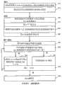
图1图解说明常规列冗余方案情况下的存储器装置,其中可仅从冗余部分使用冗余数据。所述存储器装置具有存储器单元阵列100,其被划分成用户部分102与冗余部分102′。在阵列100中的存储器单元可通过沿一行的一组字线与沿一列的一组位线来存取。所述组字线可经由行解码器130通过行地址来选择。同样地,所述组位线可经由列解码器160通过列地址来选择。通常,沿一行的存储器单元页通过对应的一组读出电路170来一起读取或写入。对应的一组数据锁存器180用来锁存已从存储器读取或要写入存储器的数据页。在读取操作结束时,经由数据输出总线192将来自所述数据锁存器的数据转移输出。同样地,在写入操作开始时,经由数据输入总线194将待写入的数据转移到所述数据锁存器。 FIG. 1 illustrates a memory device in the case of a conventional column redundancy scheme, where redundant data can be used only from the redundant portion. The memory device has an array of
通常,列地址具有一次可寻址一列内的一群组位线的粒度,因此逐列映射位线缺陷。例如,可寻址列可包含八个或十六个位线,对应于沿给定行的一字节或一数据字。 Typically, column addresses have the granularity of addressing a group of bitlines within a column at a time, thus mapping bitline defects column by column. For example, an addressable column may contain eight or sixteen bit lines, corresponding to a byte or word of data along a given row. the
当在用户部分102内识别到有缺陷列(例如112)时,提供来自冗余部分102′的替代列(例如列112′)以替换所述有缺陷列。在测试期间发现坏列且关于任何有缺陷列的信息及其替代被维持在可存储在所述存储器装置内的缺陷映射116中,例如存储在 可在通电时读取的存储器阵列(ROMFUSE区块)内。每当通电所述存储器装置时,所述缺陷映射被载入到芯片上控制器200的RAM216内以用于快速存取。 When a defective column (eg, 112) is identified within the
通常,用户仅能存取所述阵列的用户部分102而不允许存取冗余部分102′。因此,列地址范围Ay是仅用于用户存取用户部分102。一组受保护列地址Ay′是用于所述系统存取冗余部分102′。所述阵列的冗余部分102′由其自身列电路组来服务,例如冗余列解码器160′、冗余读出电路170′及冗余数据锁存器180′。 Typically, users are only able to access the
每一有缺陷列可由隔离锁存器来标记。在所述情况下,将不编程在列内寻址的字节或字而不管在用于所述列的数据锁存器内的数据且在编程验证期间已将其忽略。 Each defective column can be flagged by an isolation latch. In that case, the byte or word addressed within the column will not be programmed regardless of the data within the data latch for that column and has been ignored during program verify. the
在存储器芯片上管理有缺陷列的典型现有技术系统自身使用双向解码方案以管理坏列替换。将用户地址Ay转换成用于存取用户阵列的地址Ay或用于存取冗余阵列的地址Ay′。 Typical prior art systems that manage defective columns on a memory chip themselves use a bi-directional decoding scheme to manage bad column replacement. The user address Ay is converted into an address Ay for accessing a user array or an address Ay' for accessing a redundant array. the
在此双向解码系统中的坏列通过比较进入(用户)列地址Ay与在缺陷映射216内的坏列地址列表来管理。如果发现匹配,那么将进入列地址Ay重新指派或映射到冗余部分102′内的另一良好列地址Ay′(Ay->Ay′)。如果所述进入地址不匹配所述坏列地址,那么不改变所述进入列地址(Ay->Ay)。 Bad columns in this bidirectional decoding system are managed by comparing the incoming (user) column address Ay with the list of bad column addresses in
例如,在读出操作之后,将读取数据页锁存在所述数据锁存器内。当用户请求所述数据时,其将经由线194而串流输出到数据总线190。当地址指向坏列(例如列3)时,列冗余模块210将会停用用于所述用户阵列的地址Ay而启用地址Ay′以在所述阵列的冗余部分内寻址冗余或替代列。在所述情况下,在作业中将来自所述冗余列的数据插入经由线190′到数据输出总线192的所述串流。 For example, after a read operation, the read data page is latched in the data latches. When the user requests the data, it will be streamed out to
图2A是使用常规冗余方案的读取操作的示意性时序图。主机通过发布初始读取命令在存储器装置内启动读取操作以开始发送起始读取地址。随后发送实际的起始读取地址。然后主机发布执行读取的命令。所述存储器装置然后发出忙的信号并操作以感测数据页。所述所感测的数据页被锁存在相关联的数据锁存器内。所述页将会包括所述阵列的用户部分与冗余部分。当锁存所有数据时,所述存储器装置使用准备就绪信号来发出信号。 FIG. 2A is a schematic timing diagram of a read operation using a conventional redundancy scheme. The host initiates a read operation within the memory device by issuing an initial read command to begin sending a starting read address. The actual starting read address is then sent. The host then issues a command to perform the read. The memory device then signals busy and operates to sense a page of data. The sensed page of data is latched within an associated data latch. The page will include the user portion and the redundant portion of the array. The memory device uses a ready signal to signal when all data has been latched. the
然后,用户可通过主机请求从所述数据锁存器将数据串流输出到数据输出总线192。在所述串流输出操作期间,每当遭遇到有缺陷列的时候,将用户地址Ay切换到Ay′以寻址所述冗余部分中的对应冗余数据锁存器,以使得可在作业中将所述对应的冗余数据插入到所述串流内。当将所述冗余数据输出到所述总线时,所述存储器切换回到用户地址Ay,然后此过程继续直到到达页尾为止。 The user can then request to stream data from the data latches to the
图2B是图解说明使用常规列冗余方案的读取操作的流程图。 2B is a flow diagram illustrating a read operation using a conventional column redundancy scheme. the
通电 power ups
步骤310:将缺陷映射从非易失性存储器载入到控制器RAM。 STEP 310: Load defect map from non-volatile memory to controller RAM. the
步骤312:通过设定对应的隔离锁存器来标记坏列。 STEP 312: Flag bad columns by setting corresponding isolation latches. the
读取read
步骤320:接收读取命令以跨越多个列从存储器单元读取数据页。 STEP 320: Receive a read command to read a page of data from memory cells across multiple columns. the
步骤322:发出“忙”的信号。 Step 322: Send a "busy" signal. the
步骤324:读出所述存储器单元页并将数据锁存到对应的数据锁存器内。 Step 324: Read out the page of memory cells and latch data into corresponding data latches. the
步骤326:发出“准备就绪”的信号。 Step 326: Send a "ready" signal. the
I/O I/O
步骤330:逐列地串流输出所锁存的数据。 Step 330 : Stream out the latched data column by column. the
步骤332:待串流输出的数据的目前列地址Ay=缺陷映射中的坏列地址中的一者?如果存在匹配,那么进行到步骤334,否则进行到步骤336。 Step 332 : The current column address Ay of the data to be streamed = one of the bad column addresses in the defect map? If there is a match, then proceed to step 334 , otherwise proceed to step 336 . the
步骤334:切换到Ay′以寻址用于替代数据并插入串流内的冗余列,然后进行到步骤338。 Step 334 : Switch to Ay' to address redundant columns for replacement data and insert into the stream, then proceed to Step 338 . the
步骤336:以规则地址Ay继续,然后进行到步骤338。 STEP 336 : Continue with regular address Ay, then proceed to STEP 338 . the
步骤338:最后一个列?如果到达最后一个列,那么进行到步骤340,否则进行到步骤332中的下一个列。 Step 338: The last column? If the last column is reached, then proceed to step 340, otherwise proceed to the next column in
步骤340:读取出数据页。 Step 340: Read out the data page. the
图3A是使用传统冗余方案的写入操作的示意性时序图。在写入操作中的数据转移类似于读取操作的数据转移,除了在编程之前发生使编程数据从总线串流到所述数据锁存器。例如,当碰到有缺陷列3时,不是使数据串流到用于列3的数据锁存器,而是将其重新引导到替代列。 FIG. 3A is a schematic timing diagram of a write operation using a conventional redundancy scheme. Data transfer in a write operation is similar to that of a read operation, except that streaming of program data from the bus to the data latches occurs prior to programming. For example, when a defective column 3 is encountered, instead of streaming the data to the data latch for column 3, it is redirected to the alternate column. the
主机通过发布初始写入命令在存储器装置内启动写入操作以开始发送起始写入地址。随后发送实际的起始写入地址。然后,主机可发布信号以将写入数据从数据输入总线192串流输入到所述数据锁存器。在所述串流输入操作期间,每当遭遇到有缺陷列的时候,将用户地址Ay切换成Ay′以寻址所述冗余部分内的所述对应冗余数据锁存器,以使得可在作业中将所述对应冗余数据插入到所述对应的冗余锁存器内。当已锁存所述冗余数据时,所述存储器切换回到用户地址Ay,然后此过程继续直到到达页尾为止。 The host initiates a write operation within the memory device by issuing an initial write command to begin sending a starting write address. The actual starting write address is then sent. The host can then issue a signal to stream the write data from the
然后主机发布执行编程的命令。所述存储器装置然后发出忙的信号并操作以编程一数据页。所述页将会包括所述阵列的用户部分和冗余部分。当编程验证所有数据时,所述存储器装置发出准备就绪的信号。 The host then issues commands to perform the programming. The memory device then signals busy and operates to program a page of data. The page will include the user portion and the redundant portion of the array. The memory device signals ready when all data is program-verified. the
图3B是图解说明使用常规列冗余方案的编程操作的流程图。 3B is a flow diagram illustrating a program operation using a conventional column redundancy scheme. the
通电 power ups
步骤350:将缺陷映射从非易失性存储器载入到控制器RAM。 STEP 350: Load defect map from non-volatile memory to controller RAM. the
步骤352:通过设定对应的隔离锁存器来标记坏列。 STEP 352: Flag bad columns by setting corresponding isolation latches. the
I/O I/O
步骤360:接收写入命令以跨越多个列写入数据页。 Step 360: Receive a write command to write a page of data across multiple columns. the
步骤362:逐列地将待写入的第一数据页串流输入到数据锁存器的第一页。 Step 362 : Stream the first page of data to be written into the first page of data latches column by column. the
步骤364:待串流输出的数据的目前列地址Ay=缺陷映射中的坏列地址中的一 者?如果存在匹配,那么进行到步骤366,否则进行到步骤368。 Step 364: The current column address Ay of the data to be streamed out = one of the bad column addresses in the defect map? If there is a match, proceed to step 366, otherwise proceed to step 368. the
步骤366:切换到Ay′以寻址用于替代数据并插入串流内的冗余列,然后进行到步骤369。 Step 366 : Switch to Ay' to address redundant columns for replacement data and insert into the stream, then proceed to Step 369 . the
步骤368:以规则地址Ay继续,然后进行到步骤369。 Step 368 : Continue with regular address Ay, then proceed to step 369 . the
步骤369:最后一个列?如果到达最后一个列,那么进行到步骤370,否则进行到步骤362中的下一个列。 Step 369: The last column? If the last column is reached, then proceed to step 370, otherwise proceed to the next column in
编程 programming
步骤370:接收编程命令。 Step 370: Receive a programming command. the
步骤372:发出“忙”的信号。 Step 372: Send a "busy" signal. the
步骤374:写入所述数据页直到整页经编程验证为止。 STEP 374: Writing the page of data until the entire page is program verified. the
步骤376:发出“准备就绪”的信号。 Step 376: Send a "ready" signal. the
所述双向列选择方案在能够随机存取一列方面更具有灵活性。然而,其具有缺点,即其因为替换有缺陷列所必需的多个逻辑级而相对较慢。如先前所述,所述阵列的冗余部分被保护不受用户存取影响,因此其具有其自身独特的地址信号。在作业中在用户部分与冗余部分之间进行切换使必需在两个完全不同的寻址方案之间进行切换,且此使所述双向解码方案难以远快于20MHz数据输入或输出的速率来运行。 The bi-directional column selection scheme is more flexible in being able to access a column randomly. However, it has the disadvantage that it is relatively slow due to the multiple levels of logic necessary to replace a defective column. As previously stated, the redundant portion of the array is protected from user access and thus has its own unique address signal. Switching between the user part and the redundant part on the fly necessitates switching between two completely different addressing schemes, and this makes it difficult for the two-way decoding scheme to be implemented at rates much faster than 20MHz data input or output. run. the
远程冗余方案Remote Redundancy Solution
根据本发明的一个方面,一种远程冗余方案具有从冗余数据锁存器重定位到一组缓冲器电路的用于有缺陷存储器位置的冗余或替代数据。以此方式,冗余数据处于更易于存取的位置处,以使得一个寻址方案对于在存储器阵列与I/O总线之间交换数据是必需的。特定而言,在本远程冗余方案中,用户数据与用户数据锁存器相关联且冗余数据与冗余数据锁存器相关联,但用于存储器阵列的用户部分的地址可用于存取用户数据和替代其的任何冗余数据。当目前地址是针对良好(每有缺陷)位置时,数据总线与用户数据锁存器交换数据。另一方面,当目前地址是针对有缺陷位置时,数据总线与具有载入其内的冗余数据的远程缓冲器交换数据。 According to one aspect of the invention, a remote redundancy scheme has redundant or replacement data for defective memory locations relocated from redundant data latches to a set of buffer circuits. In this way, redundant data is in a more accessible location such that an addressing scheme is necessary to exchange data between the memory array and the I/O bus. Specifically, in this remote redundancy scheme, user data is associated with user data latches and redundant data is associated with redundant data latches, but addresses for the user portion of the memory array can be used to access User Data and any redundant data that replaces it. When the current address is for a good (every defective) location, the data bus exchanges data with the user data latch. On the other hand, when the current address is for a defective location, the data bus exchanges data with a remote buffer having redundant data loaded therein. the
在优选的实施例中,采用冗余数据缓冲器电路来缓冲与冗余部分的锁存器相关联的替代数据。仅需要用于寻址所述用户部分的寻址方案。通常,在I/O总线与所述用户部分的数据锁存器之间交换数据。当遭遇有缺陷位置时,在I/O总线与更易存取的缓冲器电路之间而非与冗余部分中的数据锁存器之间交换替代数据。 In a preferred embodiment, a redundant data buffer circuit is employed to buffer the replacement data associated with the latches of the redundant portion. Only an addressing scheme for addressing the user part is required. Typically, data is exchanged between the I/O bus and the data latches of the user part. When a defective location is encountered, substitute data is exchanged between the I/O bus and the more accessible buffer circuit rather than between the data latches in the redundant section. the
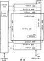
图4示意性图解说明提供实施所述远程冗余方案的背景的紧凑存储器装置的优选布置。所述存储器装置包括个别存储单元或存储器单元二维阵列400、控制电路410、行解码器420A和420B及列电路。在一个实施例中,所述存储单元个别地能够存储一位数据。在另一实施例中,所述存储单元个别地能够存储多于一个位的数据。在最优选的实施例中,所述紧凑存储器装置实施于可移除地附着到主机系统的记忆卡内。 Figure 4 schematically illustrates a preferred arrangement of compact memory devices providing a context for implementing the remote redundancy scheme. The memory device includes individual memory cells or a two-dimensional array of memory cells 400, control circuitry 410,
存储器阵列400可经由行解码器420A、420B由字线并由耦合到所述列电路的位线来寻址。所述列电路包括读出电路430A、430B、数据锁存器440A、440B及列解码 器450A、450B及数据I/O总线490。应了解,对于每一读出电路均存在一组数据锁存器。例如,在4状态存储器中,其中每一存储器单元均能够存储两位数据,可存在多个锁存器来存储两个或两个以上位的信息。用于存储多个位的一组数据锁存器揭示于2004年12月29日申请且标题为“用于读取/写入电路集合的共用处理方法及非易失性存储器(Non-Volatile Memory and Method with Shared Processing for an Aggregate ofRead/Write Circuits)”的美国专利申请案序列号11/026,536中,其全体揭示内容以引用方式并入本文中。 Memory array 400 is addressable by word lines via
在优选的实施例中,在耦合到所有偶数位线的电路430A中存在一读出电路且在耦合到所有奇数位线的电路430B中存在一读出电路。以此方式,当一起操作时,并行使用所有位线。在另一实施例中,仅每隔一位线(偶数或奇数)进行并行操作。 In a preferred embodiment, there is a readout circuit in circuit 430A coupled to all even bit lines and there is a readout circuit in
优选地,所述行解码器及所述列电路分布在阵列的两端上,以便容纳密集封装。因此,行解码器420A和420B分别部署在阵列的左侧和右侧。同样地,列电路“A”及“B”分别部署在阵列的底部及顶部。通常,列电路“A”及“B”分别存取交错位线组。例如,列电路“A”存取偶数位线而列电路“B”存取奇数位线。出于方便,除非明确注释,否则下文说明将会针对一组电路,例如“A”电路。 Preferably, the row decoders and the column circuits are distributed at both ends of the array to accommodate dense packing. Therefore,
所述列电路的读出电路430A实施为感测放大器库,其允许并行地读取或编程沿一行的存储器单元区块(又称为“页”)。在优选的实施例中,一页由一行邻接存储器单元所组成,例如1024个字节。在另一实施例中,一行存储器单元被划分成多个区块或页,例如具有偶数位线的页及具有奇数位线的页。 The readout circuitry 430A of the column circuitry is implemented as a bank of sense amplifiers that allows blocks of memory cells (also referred to as "pages") along a row to be read or programmed in parallel. In a preferred embodiment, a page consists of a row of contiguous memory cells, eg 1024 bytes. In another embodiment, a row of memory cells is divided into multiple blocks or pages, such as a page with even bit lines and a page with odd bit lines. the
控制电路410与行解码器及列电路协作以对存储器阵列400执行存储器操作。在所述控制电路中的状态机412提供存储器操作的芯片级控制。 Control circuitry 410 cooperates with row decoders and column circuitry to perform memory operations on memory array 400 . A state machine 412 in the control circuit provides chip-level control of memory operations. the
存储器阵列400被进一步划分成用户部分402和冗余部分402′。用户部分402可通过经由地址总线496提供的用户地址Ay来逐列存取。冗余部分402′无法被用户存取且具有其自身受保护的地址Ay′。所述冗余部分提供预定数目的冗余或替代列用于替换用户部分内发现的任何有缺陷列。有缺陷列的列表注册在缺陷映射416内,缺陷映射416优选地存储在非易失性存储器阵列402内。例如,冗余区域402′可提供八个替代列,每一列均是一个字节宽。此在原则上允许替换最多八个可在用户部分中发生的有缺陷列。 Memory array 400 is further divided into user portion 402 and redundant portion 402'. The user portion 402 can be accessed column by column by a user address Ay provided via the address bus 496 . The redundant part 402' cannot be accessed by the user and has its own protected address Ay'. The redundant section provides a predetermined number of redundant or replacement columns for replacing any defective columns found within the user section. A list of defective columns is registered in
然而,由于现有技术系统中冗余或替代数据在冗余列锁存器处的定位,图4中所示的优选布置的层结构可能会发生另一问题,其中所述底部及顶部列电路仅分别存取偶数列或奇数列。如果在图1中所述的现有技术系统中实施所述两层架构,那么所述底部及顶部列电路的每一者将会存取冗余部分中替代列池的一半。此是因为奇数列电路无法存取偶数替代列,且反之亦然。结果将是低效率地利用所述替代列池。例如,对于八个冗余列的池(四个偶数列与四个奇数列),可能不再替换在用户部分内偶数列中的第五个有缺陷列,即便在所述池中实际上存在八个替代列。 However, another problem may occur with the layered structure of the preferred arrangement shown in FIG. Access only even or odd columns, respectively. If the two-tier architecture were implemented in the prior art system depicted in Figure 1, each of the bottom and top column circuits would access half of the alternate column pool in the redundant section. This is because odd column circuits cannot access even alternate columns, and vice versa. The result would be an inefficient utilization of the alternate column pool. For example, for a pool of eight redundant columns (four even and four odd columns), the fifth defective column in the even Eight alternate columns. the
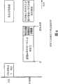
图4显示优选的实施例,其中所述冗余数据缓冲器电路与存储器装置协作以提供 远程冗余服务。与冗余部分402′相关联的冗余数据被缓冲在冗余数据缓冲器电路460内。为了清楚起见,将结合图5来描述转移到数据输出总线492的数据。将结合图6描述从所述数据输入总线所转移的数据。 Figure 4 shows a preferred embodiment wherein the redundant data buffer circuit cooperates with the memory device to provide remote redundant services. Redundant data associated with redundant portion 402 ′ is buffered within redundant
图5图解说明经配置以向所述I/O总线转移输出数据的冗余数据缓冲器电路。当一读出数据页已被锁存在所述组用户数据锁存器440A内时,在感测操作之后,可应用此转移输出模式。用户可通过经由地址总线496提供的列地址Ay来存取所述数据页内的数据。如先前所述,取决于寻址的粒度,可作为一单元来寻址一包含一预定数目位线的列。当要寻址一串列时,优选的寻址方案会是提供起始地址,后跟串长度。当列解码器450A解码列地址时,实现列选择(参见图4)。在图5中,通过来自地址总线496的指示符来示意性描述所述列选择。所述列电路还包括一组用户数据转移输出门472,其控制向I/O总线492转移选定的锁存数据。 Figure 5 illustrates a redundant data buffer circuit configured to transfer output data to the I/O bus. This transfer-out mode may be applied after a sense operation when a read data page has been latched in the set of user data latches 440A. Users can access the data within the data page through the column address Ay provided via the address bus 496 . As previously stated, depending on the granularity of addressing, a column containing a predetermined number of bit lines may be addressed as a unit. When a string of columns is to be addressed, the preferred addressing scheme would be to provide a start address followed by the string length. Column selection is achieved when column decoder 450A decodes the column address (see FIG. 4 ). In FIG. 5 , the column selection is schematically depicted by indicators from the address bus 496 . The column circuitry also includes a set of user data transfer
所述冗余数据缓冲器电路460包括冗余数据缓冲器462、一组转移输出门482、缺陷映射缓冲器466和比较电路468。所述冗余数据缓冲器缓冲来自冗余部分402′的冗余数据。在读出一数据页之后,所述冗余锁存器440A′中锁存的冗余数据被载入到冗余数据缓冲器462内。当所述冗余数据缓冲器电路460以数据输出总线492从所述冗余数据锁存器接收数据并转移到冗余数据缓冲器的模式进行配置时执行到冗余数据缓冲器462的转移,将如图6所示。同样地,缺陷映射缓冲器466缓冲在缺陷映射416内维持的缺陷列表,且在通电所述存储器装置时将其载入到缓冲器466内。 The redundant
在优选的实施例中,冗余数据缓冲器462与缺陷映射缓冲器466二者包含用于存储个别数据输入项的一组个别寄存器。有缺陷列的地址以预定义的次序存储在缺陷映射缓冲器466的个别寄存器内。同样地,与所述个别地址的每一者相关联的个别冗余数据存储在冗余数据缓冲器462内,以使得在缺陷地址与其相关联的冗余数据之间存在寄存器与寄存器的对应关系。以此方式,不同于常规的方案,所述缺陷映射不需要包含用于定位相关联的冗余数据的索引。 In a preferred embodiment, both
比较电路468是一对多比较器,其本质上提供用于所述缺陷映射缓冲器中输入项的每一者的个别比较器。每一个别比较器对共用输入地址与存储在其个别寄存器的一者内的所述缺陷映射缓冲器中的所述地址输入项的一者进行比较。在下述另一实施例中,子列解码器452视需要用来在所述冗余数据缓冲器处将寻址分解到比所述存储器阵列更精细的级。如果不实施所述选项,那么所述冗余数据缓冲器的输入地址本质上是列地址Ay。因此,当输入地址是目前寻址的列地址Ay时,其与所述缺陷映射缓冲器内所注册的所述有缺陷列的所述地址中的每一者匹配。如果根本不匹配,那么比较电路468基本上经由多个“与”门469输出不匹配信号M*。此信号M*用来启用用户数据转移输出门472,以使得数据输出总线492可从寻址的数据锁存器440A取得数据。另一方面,如果存在匹配,那么意味着目前地址位置是有缺陷列且必须代替使用其相关联的冗余数据。此通过注册匹配并输出匹配信号M的对应的个别比较器来完成。
从冗余数据缓冲器462转移冗余数据到数据输出总线492由所述组转移输出门482控制。特定而言,总线对所述冗余数据缓冲器的所述个别寄存器的每一者的存取受到对应的转移输出门的控制。因而,当目前地址匹配特定有缺陷列地址时,匹配信号M将会用于启用对应的转移输出门,以使得可将冗余数据缓冲器462的对应寄存器内的相关联冗余数据转移到数据输出总线492。Transferring redundant data from
图6是使用所述远程冗余方案的读取操作的示意性时序图。主机通过发布初始读取命令而在存储器装置内启动读取操作以开始发送起始读取地址。随后发送实际的起始读取地址。然后所述主机发布执行读取的命令。所述存储器装置以忙信号响应并进行到感测数据页。所感测数据页(包括用户部分和冗余部分)被锁存在相关联的数据锁存器440A及440A′内(参见图5)。在锁存所述数据页之后,所述远程冗余方案呼叫添加步骤,即将冗余数据从其锁存器复制到冗余数据缓冲器462。当所缓冲的数据到位时,所述存储器装置然后发出准备就绪的信号。 FIG. 6 is a schematic timing diagram of a read operation using the remote redundancy scheme. The host initiates a read operation within the memory device by issuing an initial read command to begin sending a starting read address. The actual starting read address is then sent. The host then issues a command to perform the read. The memory device responds with a busy signal and proceeds to sensing the page of data. The sensed page of data (including the user portion and the redundant portion) is latched in associated data latches 440A and 440A' (see FIG. 5 ). After latching the data page, the remote redundancy scheme calls an add step, ie copying redundant data from its latches to
然后,主机可发布读出信号以使数据从所述数据锁存器串流输出到数据输出总线492。在所述串流输出操作期间,每当遭遇到有缺陷列的时候,所述冗余数据缓冲器电路460控制所述串流输出以使数据输出总线492从冗余数据缓冲器462接收冗余数据,以使得可在作业中将对应的冗余数据插入到所述串流内。当遭遇的下一个列没有缺陷时,所述冗余数据缓冲器电路460允许数据输出总线492从所述数据锁存器440A取得数据,且此过程继续直到到达页尾为止。 The host can then issue a read signal to stream data out of the data latches to the data output bus 492 . During the stream output operation, whenever a defective column is encountered, the redundant
图7是根据优选的实施例图解说明采用所述远程冗余方案的读取操作的流程图。 Figure 7 is a flow diagram illustrating read operations employing the remote redundancy scheme, according to a preferred embodiment. the
通电 power ups
步骤510:将缺陷映射从非易失性存储器载入到缺陷映射缓冲器。 Step 510: Load the defect map from the non-volatile memory into the defect map buffer. the
读取 read
步骤520:接收读取命令以跨越多个列从存储器单元读取数据页。 STEP 520: Receive a read command to read a page of data from memory cells across multiple columns. the
步骤522:发出“忙”的信号。 Step 522: Send a "busy" signal. the
步骤524:读出所述存储器单元页并将数据锁存在对应的数据锁存器内。 STEP 524: Reading out the page of memory cells and latching data in corresponding data latches. the
步骤526:将冗余数据从冗余数据锁存器载入到冗余数据缓冲器。 Step 526: Load redundant data from redundant data latches to redundant data buffers. the
步骤528:发出“准备就绪”的信号。 Step 528: Send a "ready" signal. the
I/O I/O
步骤530:逐列地将锁存的数据串流输出到数据总线,同时执行与所述缺陷映射缓冲器内所述列地址的一对多列地址匹配。 STEP 530 : Stream latched data out to the data bus column by column while performing one-to-many column address matching with the column address in the defect mapping buffer. the
步骤532:待串流输出的数据的目前列地址Ay=缺陷映射缓冲器中的坏地址中的一者?如果存在匹配,那么进行到步骤534,否则进行到步骤536。 Step 532: Current column address Ay of the data to be streamed = one of the bad addresses in the defect mapping buffer? If there is a match, then proceed to step 534, otherwise proceed to step 536. the
步骤534:启用从冗余数据缓冲器输出替代数据到数据总线上,并进行到步骤538。 Step 534 : Enable the output of substitute data from the redundant data buffer onto the data bus, and proceed to Step 538 . the
步骤536:启用从用户数据部分输出寻址数据到数据总线上,并进行到步骤538。 STEP 536 : Enable output of addressed data from the user data section onto the data bus, and proceed to STEP 538 . the
步骤538:最后一个列?如果到达最后一个列,那么进行到步骤540,否则进行到步骤534中的下一个列。 Step 538: Last column? If the last column is reached, then proceed to step 540 , otherwise proceed to the next column in
步骤540:读出数据页。 Step 540: Read out the data page. the
因而,在本远程冗余方案中,仅使用用于所述存储器阵列的用户部分的地址。当目前地址是针对良好(没有缺陷)位置时,数据总线从所述数据锁存器取得数据。另一方面,当目前地址是针对有缺陷位置时,所述数据总线从远程缓冲器取得冗余数据。 Thus, in the present remote redundancy scheme, only addresses for the user portion of the memory array are used. When the current address is for a good (no defect) location, the data bus fetches data from the data latch. On the other hand, when the current address is for a defective location, the data bus fetches redundant data from the remote buffer. the
图8图解说明经配置以从所述I/O总线转移数据的冗余数据缓冲器电路。当将待编程数据页锁存在用户数据锁存器440A组中时,在编程操作之前可应用所述转移输入模式。所述配置类似于图5的配置,除了数据转移是在来自数据输入总线494的方向上。一组用户数据转移输入门474控制从数据输入总线494转移数据到所述数据锁存器440A。 Figure 8 illustrates a redundant data buffer circuit configured to transfer data from the I/O bus. The transfer-in mode may be applied prior to a program operation when the page of data to be programmed is latched in the set of user data latches 440A. The configuration is similar to that of FIG. 5 except that the data transfer is in the direction from the data input bus 494 . A set of user data transfer
在所述转移输入模式下,所述冗余数据缓冲器电路460也类似于图5所示的电路,除了采用一组转移输入门484而非一组转移输出门482。 In the transfer-in mode, the redundant
图9是使用所述远程冗余方案的写入操作的示意性时序图。主机通过发布初始写入命令而在存储器装置内启动写入操作以开始发送起始写入地址。随后发送实际的起始写入地址。然后,主机可发布信号以将写入数据从数据输入总线494串流输入到所述数据锁存器440A(参见图8)。在所述串流输入操作期间,每当遭遇有缺陷列的时候,所述冗余数据缓冲器电路460将有缺陷列的对应数据捕捉到冗余数据缓冲器462中。此串流过程继续直到到达页尾为止。在串流输入所述页之后,所述远程冗余方案呼叫添加步骤,即将冗余数据从冗余数据缓冲器462复制到其锁存器440A′。 FIG. 9 is a schematic timing diagram of a write operation using the remote redundancy scheme. The host initiates a write operation within the memory device by issuing an initial write command to begin sending a starting write address. The actual starting write address is then sent. The host may then issue a signal to stream write data from the data input bus 494 to the data latch 440A (see FIG. 8 ). During the stream-in operation, whenever a defective column is encountered, the redundant
然后主机发布执行编程的命令。所述存储器装置然后发出忙的信号并操作以编程一数据页。所述页将包括所述阵列的用户部分和冗余部分。当编程验证所有数据时,所述存储器装置发出准备就绪的信号。 The host then issues commands to perform the programming. The memory device then signals busy and operates to program a page of data. The page will include the user portion and the redundant portion of the array. The memory device signals ready when all data is program-verified. the
图10是根据优选的实施例图解说明采用所述远程冗余方案的编程数据载入操作的流程图。 FIG. 10 is a flowchart illustrating a programming data loading operation employing the remote redundancy scheme, according to a preferred embodiment. the
通电 power ups
步骤550:将缺陷映射从非易失性存储器载入到缺陷映射缓冲器。 Step 550: Load defect map from non-volatile memory to defect map buffer. the
I/O I/O
步骤560:接收写入命令以跨越多个列将数据页写入寻址的存储器单元。 STEP 560: Receiving a write command to write a page of data across multiple columns to the addressed memory cells. the
步骤562:逐列地从数据总线串流数据,同时执行与所述缺陷映射缓冲器内列地址的一对多列地址匹配。 STEP 562: Stream data from the data bus column by column while performing one-to-many column address matching with column addresses within the defect mapping buffer. the
步骤564:待串流输入的数据的目前列地址Ay=缺陷映射缓冲器中的坏列地址中的一者?如果存在匹配,那么进行到步骤566,否则进行到步骤570。 Step 564: Current column address Ay of the data to be streamed = one of the bad column addresses in the defect mapping buffer? If there is a match, then proceed to step 566, otherwise proceed to step 570. the
步骤566:启用从数据总线输入数据并缓冲到冗余数据缓冲器内的对应位置内。 Step 566: Enable input of data from the data bus and buffer into corresponding locations in the redundant data buffer. the
步骤568:将目前列的数据锁存器设定为“未编程”状况。进行到步骤572。 STEP 568: Set the data latches of the current column to an "unprogrammed" state. Proceed to step 572. the
步骤570:启用从数据总线输入数据并锁存到对应的数据锁存器内。 Step 570: Enable data input from the data bus and latch into corresponding data latches. the
步骤572:最后一个列?如果到达最后一个列,那么进行到步骤580,否则进行到步骤564中的下一个列。 Step 572: Last column? If the last column is reached, then proceed to step 580, otherwise proceed to the next column in
步骤580:从冗余数据缓冲器转移数据并将其锁存到对应的冗余数据锁存器。此 是一次性操作,其涉及切换到地址Ay′以存取所述冗余阵列。 STEP 580: Transferring data from redundant data buffers and latching it into corresponding redundant data latches. This is a one-time operation that involves switching to address Ay' to access the redundant array. the
编程 programming
步骤590:接收编程命令。 Step 590: Receive a programming command. the
步骤592:发出“忙”的信号。 Step 592: Send a "busy" signal. the
步骤594:写入所述锁存数据页直到整页经编程验证为止。 STEP 594: Writing the page of latched data until the entire page is program verified. the
步骤596:发出“准备就绪”的信号。 Step 596: Signal "ready". the
位级冗余支持Bit-level redundancy support
在另一实施例中,所述冗余数据缓冲器电路的地址粒度不必与所述列电路的粒度相同。优选的是,地址单元具有比列的单元更精细的分解度。例如,如果一列为一字节的宽度,以使得一次寻址一八位线群组,那么冗余数据缓冲器可在位线级处寻址。 In another embodiment, the address granularity of the redundant data buffer circuits need not be the same as that of the column circuits. Preferably, the address unit has a finer resolution than the column unit. For example, if a column is one byte wide such that eight bit line groups are addressed at a time, the redundant data buffers can be addressed at the bit line level. the
图5和图8二者均显示所述冗余数据缓冲器电路460以包括可选子列解码器452。所述子列解码器进一步将列地址Ay及列偏移地址Ay"解码成子列地址。此具有优点,即更有效率地利用冗余资源,因为可由另一冗余位线且不必由八位宽的冗余列来替换单一有缺陷位线。 Both FIGS. 5 and 8 show the redundant
多层式冗余支持Multilayer Redundancy Support
为了清楚起见,已描述了采用所述冗余数据缓冲器电路460的远程冗余方案以与一组数据锁存器一起操作,例如图4中所示的数据锁存器440A。其优点较为明显,因为仅使用用户地址而避免现有技术的较慢双向寻址方案。 For clarity, the remote redundancy scheme employing the redundant
当存在多于一组列电路运作时,还获得另一优点。如结合图4所述,由于在现有技术系统中冗余数据在替代列的锁存器处的定位,因此当存在多于一层列电路时可能会发生另一问题。例如,一组偶数列电路只能存取偶数列并因此无法使用任何奇数冗余列,对于奇数列电路也如此。本方案允许在任一数目列电路可存取的中央位置内缓冲所有冗余数据而不管其相对位置如何。 Another advantage is obtained when there are more than one set of column circuits operating. Another problem may occur when there are more than one layer of column circuitry due to the positioning of redundant data at latches of alternate columns in prior art systems, as described in connection with FIG. 4 . For example, a set of even column circuits can only access even columns and thus cannot use any odd redundant columns, and the same is true for odd column circuits. This scheme allows all redundant data to be buffered in a central location accessible to any number of column circuits regardless of their relative location. the
图11示意性图解说明服务两组数据锁存器和数据总线的冗余数据缓冲器电路。在此配置中,所述冗余数据缓冲器电路460以与图5及图8中所示的相同方式与“A”组数据锁存器440A一起操作。即使对于额外的“B”组数据锁存器440B,原理是相同的。即,所述冗余数据缓冲器电路用来控制一方面的“A”或“B”组数据锁存器与另一方面的冗余数据缓冲器462之间的总线交换。在一个实施例中,使用所述Ay地址范围进一步由层解码器480来解码用于启用数据锁存器转移的信号M以产生分别用于“A”组或“B”组的MA*或MB*启用信号。 Figure 11 schematically illustrates a redundant data buffer circuit serving two sets of data latches and a data bus. In this configuration, the redundant
因此,当所述“A”组数据锁存器处于运作时,在锁存器转移控制472A/474A上通过MA*来启用与数据锁存器440A一起的总线转移。当所述“B”组数据锁存器处于运作时,在锁存器转移控制472B/474B上通过MB*来启用与数据锁存器440B一起的总线转移。当目前地址不匹配缺陷映射缓冲器466内的所述地址的任一地址时如此。另一方面,每当存在匹配的时候,信号MA*或MB*变得不活动且缓冲器转移控制482/484通过信号M启用。此导致而是在数据总线492与冗余数据缓冲器462内的对应寄存器之间交换数据。 Thus, bus transfer with data latch 440A is enabled byMA* on latch transfer control 472A/474A when the "A" group of data latches is active. When the "B" group of data latches is active, bus transfer with data latch 440B is enabled byMB* on latch transfer control 472B/474B. This is true when the current address does not match any of the addresses within
在有缺陷列的数据锁存器内缓冲的冗余数据Redundant data buffered in the data latch of the defective column
根据本发明的另一个方面,一有缺陷列锁存冗余方案具有从所述冗余数据锁存器重定位到更容易存取的位置(例如对应的缺陷列的数据锁存器)的用于有缺陷存储器位置的冗余或替代数据。此方案是基于以下事实来论断:有缺陷列通常由于位线问题所引起而在相关联的列电路中不太多。因此,例如,在位线可能短路并变得不可使用时,其相关联的数据锁存器与列解码器可能保持运行。本发明意识到,当例如读出和编程存储器操作无法经由有缺陷位线来执行时,其列电路仍可用于缓冲数据。 In accordance with another aspect of the present invention, a defective column latch redundancy scheme has relocation from said redundant data latches to more easily accessible locations (eg, data latches of corresponding defective columns) for Redundant or replacement data for defective memory locations. This approach is justified based on the fact that defective columns are usually not too numerous in the associated column circuitry due to bit line problems. Thus, for example, while a bit line may be shorted and become unusable, its associated data latch and column decoder may remain operational. The present invention recognizes that when, for example, read and program memory operations cannot be performed via a defective bit line, its column circuitry can still be used to buffer data. the
在优选的实施例中,与有缺陷位置相关联的数据锁存器用来缓冲替代数据,所述替代数据按常规存储在与对应的冗余位置相关联的数据锁存器内。以此方式,可将用户部分视为就将数据串流到数据总线而言好像虚拟地没有缺陷一样。因此,仅需要用于寻址所述用户部分的寻址方案且在每当遭遇到有缺陷位置的时候均不需要切换到冗余数据锁存器。 In a preferred embodiment, the data latches associated with the defective locations are used to buffer replacement data that is conventionally stored in the data latches associated with the corresponding redundant locations. In this way, the user part can be treated as if virtually defect-free in terms of streaming data to the data bus. Thus, only an addressing scheme is required for addressing the user portion and there is no need to switch to redundant data latches whenever a defective location is encountered. the
在读取操作中,在感测包括用户数据与冗余数据二者的页并对其进行锁存之后,呼叫额外操作来将冗余数据复本从所述冗余数据锁存器放置到与用户部分内对应有缺陷列相关联的所述数据锁存器。以此方式,当将数据输出到数据总线时,仅需要存取所述用户数据锁存器,而不管任何有缺陷列。 In a read operation, after sensing and latching a page that includes both user data and redundant data, an additional operation is called to place a copy of redundant data from the redundant data latches to the The data latch associated with the corresponding defective column within the user portion. In this way, only the user data latches need to be accessed when outputting data to the data bus, regardless of any defective columns. the
在写入操作中,先将待写入的数据页锁存在用户数据锁存器内,而不管任何有缺陷列。以此方式,可将用户部分视为就从数据总线串流输入数据而言好像虚拟地没有缺陷一样。需要额外操作以将数据复本从与所述有缺陷列相关联的数据锁存器放置到对应的冗余数据锁存器。指示未编程状况的预定义数据也存储在有缺陷列的数据锁存器内以如此指示。然后可将包括来自所述用户数据锁存器和所述冗余数据锁存器二者的数据的整页编程在相应存储器单元内。 In a write operation, the data page to be written is first latched in the user data latches regardless of any defective columns. In this way, the user part can be treated as if virtually defect-free in terms of streaming in data from the data bus. Additional operations are required to place a copy of data from the data latch associated with the defective column to the corresponding redundant data latch. Predefined data indicating an unprogrammed condition is also stored within the data latches of the defective column to indicate so. A full page including data from both the user data latches and the redundant data latches can then be programmed within the respective memory cells. the
图12示意性图解说明提供实施有缺陷列锁存冗余方案的背景的紧凑存储器装置的优选布置。所述存储器装置本质上具有如图4所示的一类似结构,但不需要冗余数据缓冲器电路460。特定而言,所述存储器装置包括二维存储器单元阵列400、控制电路610、行解码器420A及420B和列电路。 Figure 12 schematically illustrates a preferred arrangement of a compact memory device providing a context for implementing a defective column latch redundancy scheme. The memory device essentially has a similar structure as shown in FIG. 4 , but without redundant
存储器阵列400可经由行解码器420A、420B通过字线且通过耦合到所述列电路的位线来寻址。所述列电路包括读出电路430A、430B、数据锁存器640A、640B及列解码器450A、450B和数据I/O总线490。如先前结合图4所述,应了解针对每一读出电路存在一组数据锁存器。 Memory array 400 is addressable by word lines via
在优选的实施例中,在耦合到所有偶数位线的电路430A中存在读出电路且在耦合到所有奇数位线的电路430B中存在读出电路。以此方式,当一起操作时,并行使用所有位线。在另一实施例中,仅对每隔一位线(偶数或奇数)进行并行操作。 In a preferred embodiment, there is a readout circuit in circuit 430A coupled to all even bit lines and a readout circuit in
所述行解码器及所述列电路优选地分布在阵列的两端上,以便容纳密集封装。因此,行解码器420A及420B分别部署在阵列的左侧和右侧。同样地,列电路“A”及“B”分别部署在阵列的底部和顶部。通常,列电路“A”及“B”分别存取交错的位线组。例如,列电路“A”存取偶数位线而列电路“B”存取奇数位线。为方便起见,除非明确注释,否则下文说明将针对一组通用电路,其中去掉数字参考中的“A”或“B”附加物。 The row decoders and the column circuitry are preferably distributed across the array to accommodate dense packing. Therefore,
所述列电路的感应电路430实施为感测放大器库,其允许并行地读取或编程沿一行的存储器单元区块(又称为一“页”)。在优选的实施例中,一页是由一行邻接存储器单元所组成,例如1024个字节。在另一实施例中,其中一行存储器单元被划分成多个区块或页。 The sense circuits 430 of the column circuits are implemented as banks of sense amplifiers that allow blocks of memory cells along a row (also referred to as a "page") to be read or programmed in parallel. In a preferred embodiment, a page consists of a row of contiguous memory cells, eg 1024 bytes. In another embodiment, one row of memory cells is divided into multiple blocks or pages. the
控制电路610与行解码器及列电路协作以对存储器阵列400执行存储器操作。在所述控制电路内的状态机612提供存储器操作的芯片级控制。
存储器阵列400被进一步划分成用户部分402和冗余部分402′。用户部分402可通过经由地址总线496提供的用户地址Ay来逐列存取。冗余部分402′无法被用户存取且具有其自身受保护的地址Ay′。所述冗余部分提供预定数目的冗余或替代列用于替换用户部分内发现的任何有缺陷列。有缺陷列的列表注册在缺陷映射416中,缺陷映射416优选地存储在非易失性存储器阵列402内。例如,冗余区域402′可提供八个替代列,每一列均是一个字节宽。此在原则上允许最多替换八个可在用户部分中发生的有缺陷列。 Memory array 400 is further divided into user portion 402 and redundant portion 402'. The user portion 402 can be accessed column by column by a user address Ay provided via the address bus 496 . The redundant part 402' cannot be accessed by the user and has its own protected address Ay'. The redundant section provides a predetermined number of redundant or replacement columns for replacing any defective columns found within the user section. A list of defective columns is registered in
在如图12所示的列电路结构中,在用户数据锁存器640群组与数据输入总线494之间的数据交换由用户列解码器450来控制。用户列解码器450解码用户列地址Ay并允许存取用户列内的数据锁存器群组以存取数据输入总线494。同样地,在冗余数据锁存器640′群组与数据输入总线494之间的数据交换由冗余列解码器450′来控制。冗余列解码器450′解码冗余列地址Ay′并允许存取冗余列内的数据锁存器群组以存取I/O总线。 In the column circuit configuration shown in FIG. 12 , data exchange between the group of user data latches 640 and the data input bus 494 is controlled by the user column decoder 450 . The user column decoder 450 decodes the user column address Ay and allows access to a group of data latches within the user column to access the data input bus 494 . Likewise, data exchange between groups of redundant data latches 640' and data input bus 494 is controlled by redundant column decoder 450'. The redundant column decoder 450' decodes the redundant column address Ay' and allows access to the group of data latches within the redundant column to access the I/O bus. the
本发明提供额外的结构以允许在用户列的数据锁存器与冗余列之间往返数据。 The present invention provides additional structures to allow data to be shuttled between the user column's data latches and the redundant column. the
图13示意性图解说明数据锁存器缓冲器,其用于在所述用户数据锁存器与冗余数据锁存器之间往返数据,以便实施另一列冗余方案而不必采用双向寻址。 Figure 13 schematically illustrates a data latch buffer used to shuttle data between the user data latches and redundant data latches in order to implement another column redundancy scheme without having to employ bi-directional addressing. the
在优选的实施例中,在输出数据总线492与输入数据总线494之间提供数据锁存器缓冲器620。数据锁存器缓冲器620包括串列连接的第一移位寄存器622和第二移位寄存器624。第一移位寄存器622和第二移位寄存器624以管线方式操作,其中来自输出总线492的数据单元通过所述两个寄存器被偏移并在时钟信号CLK控制下逐个单元地返回到输入总线494。以此方式,可同时对I/O总线490的输出及输入部分二者进行操作。 In a preferred embodiment, a data latch buffer 620 is provided between the output data bus 492 and the input data bus 494 . The data latch buffer 620 includes a
控制电路610在用户列与冗余列的数据锁存器之间提供寻址与转移控制。例如,在将一数据页锁存在用户数据锁存器450与冗余数据锁存器450′内之后,在所述冗余数据锁存器450′内的数据将会被复制到所述有缺陷列的对应数据锁存器。控制电路610向冗余列解码器450′提供冗余列地址Ay′并经由数据输出总线492从冗余数据锁存器 640′逐一将所述冗余数据单元偏移到数据锁存器缓冲器620内。所述经偏移冗余数据单元会从所述数据锁存器缓冲器的另一端出现并进入输入数据总线494。通过参照载入到控制电路610中的缺陷映射616,产生对应的有缺陷列地址Ay并由用户列解码器450用以将所述冗余数据单元引导到其在所述有缺陷列内的对应锁存器。
类似原理适用于从所述有缺陷列的数据锁存器到对应的冗余数据锁存器的转移。在此情况下,基于所述缺陷映射,逐一地存取所述有缺陷列的数据锁存器并偏移通过数据锁存器缓冲器620。在所述数据锁存器缓冲器的另一端处,所述冗余数据单元经由冗余列解码器450′适当地解码Ay′来引导到其相应的冗余数据锁存器。 Similar principles apply for the transfer from the defective column's data latch to the corresponding redundant data latch. In this case, the data latches of the defective column are accessed one by one and shifted through the data latch buffer 620 based on the defect map. At the other end of the data latch buffer, the redundant data units are directed to their corresponding redundant data latches via redundant column decoder 450' by properly decoding Ay'. the
图14是使用所述有缺陷列锁存冗余方案的读取操作的示意性时序图。主机通过发布初始读取命令而在存储器装置内启动读取操作以开始发送起始读取地址。随后发送实际的起始读取地址。然后主机发布执行读取的命令。所述存储器装置以忙的信号响应并进行到感测一数据页。所述感测的数据页(包括用户部分和冗余部分)被锁存到相关联的数据锁存器440A及440A′内(参见图13)。在锁存所述数据页之后,所述有缺陷列锁存冗余方案呼叫添加步骤,即将冗余数据从其锁存器复制到对应有缺陷列的数据锁存器。在所述对应的有缺陷列内锁存所述冗余数据之后,所述存储器装置然后发出准备就绪的信号。本质上,当所述存储器装置具有预定义的时序规格时,必须在忙与准别就需所界定的周期所允许的最大时间内完成所述添加步骤。 FIG. 14 is a schematic timing diagram of a read operation using the defective column latch redundancy scheme. The host initiates a read operation within the memory device by issuing an initial read command to begin sending a starting read address. The actual starting read address is then sent. The host then issues a command to perform the read. The memory device responds with a busy signal and proceeds to sensing a page of data. The sensed page of data (including the user portion and the redundant portion) is latched into associated data latches 440A and 440A' (see FIG. 13 ). After latching the data page, the defective column latch redundancy scheme calls an add step of copying redundant data from its latches to the corresponding defective column's data latches. After latching the redundant data in the corresponding defective column, the memory device then signals ready. Essentially, when the memory device has predefined timing specifications, the adding step must be done within the maximum time allowed by the period defined by busy and ready. the
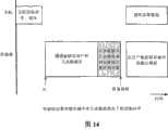
然后,主机可发布读出信号以使数据从所述用户数据锁存器440串流输出到数据输出总线492。由于所述有缺陷列的数据锁存器现在包含对应的冗余数据,因此不需要如同常规情况那样,使用第二组地址Ay′来从所述冗余数据锁存器440′检索。 The host can then issue a read signal to stream data out from the user data latch 440 to the data output bus 492 . Since the data latches of the defective column now contain corresponding redundant data, there is no need to use the second set of addresses Ay' to retrieve from the redundant data latches 440', as is conventionally the case. the
图15是根据优选的实施例图解说明采用有缺陷列锁存冗余方案的读取操作的流程图。 Figure 15 is a flowchart illustrating a read operation using a defective column latch redundancy scheme according to a preferred embodiment. the
通电 power ups
步骤710:将缺陷映射从非易失性存储器载入到控制器RAM。 STEP 710: Load defect map from non-volatile memory to controller RAM. the
读取 read
步骤720:接收读取命令用于跨越多个列从存储器单元读取包括用户数据和冗余数据的页。 STEP 720: Receive a read command for reading a page including user data and redundant data from memory cells across multiple columns. the
步骤722:发出“忙”的信号。 Step 722: Send a "busy" signal. the
步骤724:读出所述存储器单元页并将数据锁存到对应的数据锁存器内。 Step 724: Read out the page of memory cells and latch data into corresponding data latches. the
步骤726:将数据从冗余数据锁存器复制到对应有缺陷列的数据锁存器。 STEP 726: Copy data from redundant data latches to data latches corresponding to defective columns. the
步骤728:发出“准备就绪”的信号。 Step 728: Send a "ready" signal. the
I/O I/O
步骤730:逐列地使数据从用户数据锁存器串流输出到数据总线而不管有缺陷列。 STEP 730: Streaming data out of the user data latches to the data bus column by column regardless of defective columns. the
步骤740:读出所述数据页。 Step 740: Read the data page. the
因此,在本有缺陷列锁存冗余方案中,仅使用用于存储器阵列的用户部分的地址来使数据串流输出且仅需要存取所述用户数据锁存器。Thus, in the present defective column latch redundancy scheme, only the addresses for the user portion of the memory array are used to stream data out and only the user data latches need to be accessed.
图16是使用所述有缺陷列锁存冗余方案的写入操作的示意性时序图。主机通过发布初始写入命令而在存储器装置内启动写入操作以开始发送起始写入地址。随后发送实际的起始写入地址。然后,主机可发布信号以将写入数据从数据输入总线494串流输入到所述数据锁存器440(参见图8)而不管对应的列是否有缺陷。然后主机发布执行编程的命令。所述存储器装置然后如同正在进行编程一数据页那样地发出忙的信号。然而,所述控制电路(参加图13)推迟实际的编程,因为所述有缺陷列锁存冗余方案呼叫添加步骤,即将数据从所述有缺陷列的锁存器复制到对应的冗余列的冗余数据锁存器。在复制所述数据之后,所述有缺陷列的锁存器被设定为预定值以指示未编程状况。 FIG. 16 is a schematic timing diagram of a write operation using the defective column latch redundancy scheme. The host initiates a write operation within the memory device by issuing an initial write command to begin sending a starting write address. The actual starting write address is then sent. The host can then issue a signal to stream write data from the data input bus 494 to the data latch 440 (see FIG. 8 ) regardless of whether the corresponding column is defective. The host then issues commands to perform the programming. The memory device then signals busy as if a page of data was being programmed. However, the control circuit (see FIG. 13 ) postpones the actual programming because the defective column latch redundancy scheme calls for an additional step of copying data from the defective column's latch to the corresponding redundant column redundant data latches. After the data is copied, the latch of the defective column is set to a predetermined value to indicate an unprogrammed condition. the
然后所述控制电路进行到在所述存储器中编程所述页。所述页将包括所述阵列的用户部分和冗余部分。当编程验证所有数据时,所述存储器装置发出准备就绪的信号。 The control circuitry then proceeds to program the page in the memory. The page will include the user portion and the redundant portion of the array. The memory device signals ready when all data is program-verified. the
图17是根据优选的实施例图解说明采用有缺陷列锁存冗余方案的编程数据载入操作的流程图。 17 is a flowchart illustrating a program data load operation using a defective column latch redundancy scheme according to a preferred embodiment. the
通电 power ups
步骤760:将缺陷映射从非易失性存储器载入到控制器RAM。 STEP 760: Load defect map from non-volatile memory to controller RAM. the
I/O I/O
步骤770:接收写入命令以跨越多个列将一数据页写入到所寻址的存储器单元。 STEP 770: Receive a write command to write a page of data to addressed memory cells across multiple columns. the
步骤772:将待写入的数据页串流到用户数据锁存器中,不管有否任何有缺陷列。 STEP 772: Stream the page of data to be written into the user data latches regardless of any defective columns. the
步骤774:发出“忙”信号。 Step 774: Send a "busy" signal. the
用户数据锁存器到冗余数据锁存器的转移 Transfer of user data latches to redundant data latches
步骤776:将数据从有缺陷列的用户锁存器转移到冗余列的对应冗余锁存器。 STEP 776: Transferring data from the user latch of the defective column to the corresponding redundant latch of the redundant column. the
步骤778:通过将预定义数据值写入到所有有缺陷列的相关联的用户数据锁存器的每一者内来标记所有有缺陷列。 STEP 778: Flag all defective columns by writing a predefined data value into each of their associated user data latches. the
编程 programming
步骤780:接收编程命令。 Step 780: Receive a programming command. the
步骤782:写入包括用户和冗余数据的页直到整页经编程验证为止。 STEP 782: Writing the page including user and redundancy data until the entire page is program verified. the
步骤784:发出“准备就绪”信号。 Step 784: Send a "ready" signal. the
尽管使用各种列冗余方案的实例进行了说明,但所属技术领域的技术人员应容易地了解用于有缺陷存储器位置的其它替换单元也可行。 Although illustrated using examples of various column redundancy schemes, those skilled in the art will readily appreciate that other replacement cells for defective memory locations are also possible. the
虽然已经针对特定实施例描述本发明的各个方面,但应了解,本发明受到所附权利要求书的完整范围的保护。While various aspects of the invention have been described with respect to particular embodiments, it is to be understood that the invention is protected by the full scope of the appended claims.
Claims (24)
- One kind in nonvolatile memory array from the user array part of crossing over described storer and the redundant array method of reading out data the two the memory location group partly, described nonvolatile memory array is divided into described user array part and redundant array part, so that the defectiveness position in the described user array part can be replaced by the corresponding redundant position in the described redundant array part, described method comprises:One access circuit group is provided, and it comprises be used to the user data latch group that latchs the data that partly are associated with described user array with for the redundant latch storage group that latchs the data that partly are associated with described redundant array;Data bus is provided;The address of the defectiveness position of the described user array part of buffering in defective mapping impact damper;Buffering is from the redundant data of the data latches of described redundant array part in the redundant data impact damper; AndPresent address in response to the defectiveness position in the described defective mapping of not corresponding to of the described user array part impact damper, enable the exchanges data between described data bus and the described user array described data latches partly, and in response to the present address corresponding to the defectiveness position in the described defective mapping impact damper of described user array part, enable the exchanges data between the interior corresponding redundant data of described data bus and described redundant data impact damper.
- 2. the method for claim 1, wherein:Can come the described memory array of addressing by row and row; AndDescribed defectiveness position is can be by the defectiveness row of replacing from the redundant columns of described redundant array part.
- 3. the method for claim 1, wherein:Described present address is can not the described redundant array part of directly address for the described user array part of addressing.
- 4. the method for claim 1, wherein:Described exchanges data of enabling between the redundant data corresponding in described data bus and the described redundant data impact damper is to transfer on the direction of described data bus at during read operations.
- 5. the method for claim 1, wherein:Described exchanges data of enabling between the redundant data corresponding in described data bus and the described redundant data impact damper be during the write operation on the direction of described data bus reception.
- 6. the method for claim 1, wherein:Can be with coming described redundant data in the addressing redundant data impact damper than being used for described user array part and the redundant array meticulousr addressable unit of addressable unit partly.
- 7. the method for claim 1, wherein:Described access circuit group through coupling with a plurality of access circuit group that operates with described redundant data impact damper and described data bus among.
- 8. the method for claim 1, wherein:Described a plurality of access circuit group is not operating in the overlapping address scope.
- 9. the method for claim 1, wherein said array of non-volatile memory cells is quickflashing EEPROM.
- 10. the method for claim 1, wherein said array of non-volatile memory cells is included in the memory card.
- 11. such as the described method of arbitrary claim in the claim 1 to 10, wherein individual memory cell is stored two one in the memory state separately.
- 12. such as the described method of arbitrary claim in the claim 1 to 10, wherein individual memory cell is stored separately more than the one in two memory states.
- 13. a nonvolatile memory, it comprises:The memory array of non-volatile memory cells, it is divided into user array part and redundant array part, so that the defectiveness position in the described user array part can be replaced by the redundant position in the described redundant array part;One access circuit group, it comprises be used to the user data latch group that latchs the data that partly are associated with described user array with for the redundant latch storage group that latchs the data that partly are associated with described redundant array;Data bus;Defective mapping impact damper, it is used for storing the address of described user array defectiveness position partly;The redundant data impact damper, it is used for storage from the redundant data of the data latches of described redundant array part; AndThe redundant data Buffer control circuit, it enables the exchanges data between the described data latches of described data bus and described user array part in response to the present address of the defectiveness position in the described defective mapping of not corresponding to of the described user array part impact damper, and shining upon the present address of the defectiveness position in the impact damper and enabling exchanges data between described data bus and the described redundant data impact damper corresponding to described defective in response to described user array part.
- 14. nonvolatile memory as claimed in claim 13, wherein:Described memory array can be come addressing by row and row; AndDescribed defectiveness position is can be by the defectiveness row of replacing from the redundant columns of described redundant array part.
- 15. nonvolatile memory as claimed in claim 13, wherein:Described present address is can not the described redundant array part of directly address for the described user array part of addressing.
- 16. nonvolatile memory as claimed in claim 13, wherein:Described redundant data impact damper is through enabling will corresponding to the redundant data of described defectiveness position transfer to described data bus during corresponding to the address of described defectiveness position at during read operations when described present address.
- 17. nonvolatile memory as claimed in claim 13, wherein:Described redundant data impact damper is through enabling to receive redundant data corresponding to described defectiveness position from described data bus during corresponding to the address of described defectiveness position when described present address during the write operation.
- 18. nonvolatile memory as claimed in claim 13, wherein:Described redundant data Buffer control circuit and redundant data impact damper have than the meticulousr addressable unit of addressable unit that is used for described user array part and redundant array part.
- 19. nonvolatile memory as claimed in claim 13, wherein:The access circuit that operates with described redundant data impact damper cushions therein in the not overlapping address scope of some described redundant data at least and operates.
- 20. nonvolatile memory as claimed in claim 19, wherein:Described access circuit is the one in a plurality of access circuits that described redundant data impact damper operates.
- 21. nonvolatile memory as claimed in claim 13, wherein said array of non-volatile memory cells are quickflashing EEPROM.
- 22. nonvolatile memory as claimed in claim 13, wherein said array of non-volatile memory cells is included in the memory card.
- 23. such as the described nonvolatile memory of arbitrary claim in the claim 13 to 22, wherein individual memory cell is stored two one in the memory state separately.
- 24. such as the described nonvolatile memory of arbitrary claim in the claim 13 to 22, wherein individual memory cell is stored separately more than the one in two memory states.
Applications Claiming Priority (5)
| Application Number | Priority Date | Filing Date | Title |
|---|---|---|---|
| US11/388,579 | 2006-03-24 | ||
| US11/389,411US7324389B2 (en) | 2006-03-24 | 2006-03-24 | Non-volatile memory with redundancy data buffered in remote buffer circuits |
| US11/388,579US7352635B2 (en) | 2006-03-24 | 2006-03-24 | Method for remote redundancy for non-volatile memory |
| US11/389,411 | 2006-03-24 | ||
| PCT/US2007/063912WO2007112202A2 (en) | 2006-03-24 | 2007-03-13 | Non-volatile memory and method with redundancy data buffered in remote buffer circuits |
Publications (2)
| Publication Number | Publication Date |
|---|---|
| CN101421797A CN101421797A (en) | 2009-04-29 |
| CN101421797Btrue CN101421797B (en) | 2013-03-27 |
Family
ID=38533210
Family Applications (1)
| Application Number | Title | Priority Date | Filing Date |
|---|---|---|---|
| CN2007800135346AExpired - Fee RelatedCN101421797B (en) | 2006-03-24 | 2007-03-13 | Non-volatile memory and method with redundancy data buffered in remote buffer circuits |
Country Status (2)
| Country | Link |
|---|---|
| US (1) | US7352635B2 (en) |
| CN (1) | CN101421797B (en) |
Families Citing this family (22)
| Publication number | Priority date | Publication date | Assignee | Title |
|---|---|---|---|---|
| US7394690B2 (en)* | 2006-03-24 | 2008-07-01 | Sandisk Corporation | Method for column redundancy using data latches in solid-state memories |
| US7324389B2 (en)* | 2006-03-24 | 2008-01-29 | Sandisk Corporation | Non-volatile memory with redundancy data buffered in remote buffer circuits |
| US8102705B2 (en)* | 2009-06-05 | 2012-01-24 | Sandisk Technologies Inc. | Structure and method for shuffling data within non-volatile memory devices |
| US20110002169A1 (en) | 2009-07-06 | 2011-01-06 | Yan Li | Bad Column Management with Bit Information in Non-Volatile Memory Systems |
| US8725935B2 (en) | 2009-12-18 | 2014-05-13 | Sandisk Technologies Inc. | Balanced performance for on-chip folding of non-volatile memories |
| US8238178B2 (en)* | 2010-02-12 | 2012-08-07 | Taiwan Semiconductor Manufacturing Company, Ltd. | Redundancy circuits and operating methods thereof |
| KR101100958B1 (en)* | 2010-09-06 | 2011-12-29 | 주식회사 하이닉스반도체 | Nonvolatile memory device |
| KR101196907B1 (en) | 2010-10-27 | 2012-11-05 | 에스케이하이닉스 주식회사 | Semiconductor memory device and method of operation thereof |
| US8472280B2 (en) | 2010-12-21 | 2013-06-25 | Sandisk Technologies Inc. | Alternate page by page programming scheme |
| US9342446B2 (en) | 2011-03-29 | 2016-05-17 | SanDisk Technologies, Inc. | Non-volatile memory system allowing reverse eviction of data updates to non-volatile binary cache |
| US8842473B2 (en)* | 2012-03-15 | 2014-09-23 | Sandisk Technologies Inc. | Techniques for accessing column selecting shift register with skipped entries in non-volatile memories |
| US9934872B2 (en) | 2014-10-30 | 2018-04-03 | Sandisk Technologies Llc | Erase stress and delta erase loop count methods for various fail modes in non-volatile memory |
| US9773571B2 (en)* | 2014-12-16 | 2017-09-26 | Macronix International Co., Ltd. | Memory repair redundancy with array cache redundancy |
| US9224502B1 (en) | 2015-01-14 | 2015-12-29 | Sandisk Technologies Inc. | Techniques for detection and treating memory hole to local interconnect marginality defects |
| US10032524B2 (en) | 2015-02-09 | 2018-07-24 | Sandisk Technologies Llc | Techniques for determining local interconnect defects |
| US9564219B2 (en) | 2015-04-08 | 2017-02-07 | Sandisk Technologies Llc | Current based detection and recording of memory hole-interconnect spacing defects |
| US9269446B1 (en) | 2015-04-08 | 2016-02-23 | Sandisk Technologies Inc. | Methods to improve programming of slow cells |
| KR102415835B1 (en)* | 2016-01-08 | 2022-07-01 | 삼성전자주식회사 | A semiconductor memory device, and a memory system including the semiconductor memory device |
| US9741421B1 (en)* | 2016-04-05 | 2017-08-22 | Micron Technology, Inc. | Refresh circuitry |
| CN108536389A (en)* | 2017-03-06 | 2018-09-14 | 北京兆易创新科技股份有限公司 | Row replacement method, device and NAND memory device based on nand flash memory |
| US11354209B2 (en)* | 2020-04-13 | 2022-06-07 | Sandisk Technologies Llc | Column redundancy data architecture for yield improvement |
| US11567868B2 (en)* | 2020-11-13 | 2023-01-31 | Taiwan Semiconductor Manufacturing Company, Ltd. | Method for copying data within memory device, memory device, and electronic device thereof |
Citations (2)
| Publication number | Priority date | Publication date | Assignee | Title |
|---|---|---|---|---|
| US6104646A (en)* | 1997-08-28 | 2000-08-15 | Kabushiki Kaisha Toshiba | Semiconductor memory device having redundancy circuit with high rescue efficiency |
| US6816420B1 (en)* | 2003-07-29 | 2004-11-09 | Xilinx, Inc. | Column redundancy scheme for serially programmable integrated circuits |
Family Cites Families (27)
| Publication number | Priority date | Publication date | Assignee | Title |
|---|---|---|---|---|
| US4281389A (en) | 1979-06-22 | 1981-07-28 | Smith Kent G | Pacing timer mounting arrangement |
| US4281398A (en)* | 1980-02-12 | 1981-07-28 | Mostek Corporation | Block redundancy for memory array |
| US5095344A (en) | 1988-06-08 | 1992-03-10 | Eliyahou Harari | Highly compact eprom and flash eeprom devices |
| US5070032A (en) | 1989-03-15 | 1991-12-03 | Sundisk Corporation | Method of making dense flash eeprom semiconductor memory structures |
| EP0935255A2 (en) | 1989-04-13 | 1999-08-11 | SanDisk Corporation | Flash EEPROM system |
| US5172338B1 (en) | 1989-04-13 | 1997-07-08 | Sandisk Corp | Multi-state eeprom read and write circuits and techniques |
| US5200959A (en) | 1989-10-17 | 1993-04-06 | Sundisk Corporation | Device and method for defect handling in semi-conductor memory |
| JP2900451B2 (en) | 1989-11-30 | 1999-06-02 | ソニー株式会社 | Memory device |
| JPH03214500A (en) | 1990-01-18 | 1991-09-19 | Sony Corp | Memory device |
| US5343063A (en) | 1990-12-18 | 1994-08-30 | Sundisk Corporation | Dense vertical programmable read only memory cell structure and processes for making them |
| US5313421A (en) | 1992-01-14 | 1994-05-17 | Sundisk Corporation | EEPROM with split gate source side injection |
| US6222762B1 (en) | 1992-01-14 | 2001-04-24 | Sandisk Corporation | Multi-state memory |
| US5315541A (en) | 1992-07-24 | 1994-05-24 | Sundisk Corporation | Segmented column memory array |
| US5428621A (en) | 1992-09-21 | 1995-06-27 | Sundisk Corporation | Latent defect handling in EEPROM devices |
| US5555204A (en) | 1993-06-29 | 1996-09-10 | Kabushiki Kaisha Toshiba | Non-volatile semiconductor memory device |
| KR0169267B1 (en) | 1993-09-21 | 1999-02-01 | 사토 후미오 | Nonvolatile Semiconductor Memory |
| US5661053A (en) | 1994-05-25 | 1997-08-26 | Sandisk Corporation | Method of making dense flash EEPROM cell array and peripheral supporting circuits formed in deposited field oxide with the use of spacers |
| US5627786A (en) | 1995-02-10 | 1997-05-06 | Micron Quantum Devices, Inc. | Parallel processing redundancy scheme for faster access times and lower die area |
| US5903495A (en) | 1996-03-18 | 1999-05-11 | Kabushiki Kaisha Toshiba | Semiconductor device and memory system |
| US5768192A (en) | 1996-07-23 | 1998-06-16 | Saifun Semiconductors, Ltd. | Non-volatile semiconductor memory cell utilizing asymmetrical charge trapping |
| US6768165B1 (en) | 1997-08-01 | 2004-07-27 | Saifun Semiconductors Ltd. | Two bit non-volatile electrically erasable and programmable semiconductor memory cell utilizing asymmetrical charge trapping |
| JP2000195291A (en) | 1998-12-28 | 2000-07-14 | Oki Electric Ind Co Ltd | Semiconductor storage device and its redundancy relieving method |
| JP2000235800A (en) | 1999-02-12 | 2000-08-29 | Mitsubishi Electric Corp | Semiconductor storage device |
| KR100380346B1 (en) | 2000-10-16 | 2003-04-11 | 삼성전자주식회사 | Semiconductor memory device with redundancy logic cell and repairable method |
| US7170802B2 (en) | 2003-12-31 | 2007-01-30 | Sandisk Corporation | Flexible and area efficient column redundancy for non-volatile memories |
| US6868021B2 (en) | 2002-09-27 | 2005-03-15 | Oki Electric Industry Co., Ltd. | Rapidly testable semiconductor memory device |
| US20060140007A1 (en) | 2004-12-29 | 2006-06-29 | Raul-Adrian Cernea | Non-volatile memory and method with shared processing for an aggregate of read/write circuits |
- 2006
- 2006-03-24USUS11/388,579patent/US7352635B2/ennot_activeExpired - Fee Related
- 2007
- 2007-03-13CNCN2007800135346Apatent/CN101421797B/ennot_activeExpired - Fee Related
Patent Citations (2)
| Publication number | Priority date | Publication date | Assignee | Title |
|---|---|---|---|---|
| US6104646A (en)* | 1997-08-28 | 2000-08-15 | Kabushiki Kaisha Toshiba | Semiconductor memory device having redundancy circuit with high rescue efficiency |
| US6816420B1 (en)* | 2003-07-29 | 2004-11-09 | Xilinx, Inc. | Column redundancy scheme for serially programmable integrated circuits |
Also Published As
| Publication number | Publication date |
|---|---|
| CN101421797A (en) | 2009-04-29 |
| US20070223291A1 (en) | 2007-09-27 |
| US7352635B2 (en) | 2008-04-01 |
Similar Documents
| Publication | Publication Date | Title |
|---|---|---|
| CN101421797B (en) | Non-volatile memory and method with redundancy data buffered in remote buffer circuits | |
| US7394690B2 (en) | Method for column redundancy using data latches in solid-state memories | |
| US7224605B1 (en) | Non-volatile memory with redundancy data buffered in data latches for defective locations | |
| US7324389B2 (en) | Non-volatile memory with redundancy data buffered in remote buffer circuits | |
| US8619493B2 (en) | Flexible memory operations in NAND flash devices | |
| CN102971796B (en) | Nonvolatile memory and method for even/odd combined interleaved block decoding with adaptive word line activation circuit | |
| WO2011005663A1 (en) | Bad column management with bit information in non-volatile memory systems | |
| JP2012181916A (en) | Multiple independent serial link memory | |
| JP2007517353A (en) | Flexible and area efficient column redundancy for non-volatile memory | |
| JP2008524748A (en) | Data relocation in memory systems | |
| WO2013165774A1 (en) | Column redundancy circuitry for non-volatile memory | |
| EP2002447B1 (en) | Non-volatile memory and method with redundancy data buffered in remote buffer circuits | |
| EP2008283B1 (en) | Non-volatile memory and method with redundancy data buffered in data latches for defective locations |
Legal Events
| Date | Code | Title | Description |
|---|---|---|---|
| C06 | Publication | ||
| PB01 | Publication | ||
| C10 | Entry into substantive examination | ||
| SE01 | Entry into force of request for substantive examination | ||
| ASS | Succession or assignment of patent right | Owner name:SANDISK TECHNOLOGY CO., LTD. Free format text:FORMER OWNER: SANDISK CORP. Effective date:20130218 | |
| C41 | Transfer of patent application or patent right or utility model | ||
| TA01 | Transfer of patent application right | Effective date of registration:20130218 Address after:American Texas Applicant after:Sandisk Corp. Address before:American California Applicant before:Sandisk Corp. | |
| C14 | Grant of patent or utility model | ||
| GR01 | Patent grant | ||
| C56 | Change in the name or address of the patentee | ||
| CP01 | Change in the name or title of a patent holder | Address after:American Texas Patentee after:DELPHI INT OPERATIONS LUX SRL Address before:American Texas Patentee before:Sandisk Corp. | |
| CF01 | Termination of patent right due to non-payment of annual fee | ||
| CF01 | Termination of patent right due to non-payment of annual fee | Granted publication date:20130327 Termination date:20200313 |