CN101420840A - Sheet structure and method of manufacturing the same - Google Patents
Sheet structure and method of manufacturing the sameDownload PDFInfo
- Publication number
- CN101420840A CN101420840ACNA2008101700890ACN200810170089ACN101420840ACN 101420840 ACN101420840 ACN 101420840ACN A2008101700890 ACNA2008101700890 ACN A2008101700890ACN 200810170089 ACN200810170089 ACN 200810170089ACN 101420840 ACN101420840 ACN 101420840A
- Authority
- CN
- China
- Prior art keywords
- carbon nanotube
- bundles
- linear
- bundle
- substrate
- Prior art date
- Legal status (The legal status is an assumption and is not a legal conclusion. Google has not performed a legal analysis and makes no representation as to the accuracy of the status listed.)
- Pending
Links
Images


Classifications
- H—ELECTRICITY
- H01—ELECTRIC ELEMENTS
- H01L—SEMICONDUCTOR DEVICES NOT COVERED BY CLASS H10
- H01L23/00—Details of semiconductor or other solid state devices
- H01L23/34—Arrangements for cooling, heating, ventilating or temperature compensation ; Temperature sensing arrangements
- H01L23/36—Selection of materials, or shaping, to facilitate cooling or heating, e.g. heatsinks
- H01L23/373—Cooling facilitated by selection of materials for the device or materials for thermal expansion adaptation, e.g. carbon
- H—ELECTRICITY
- H01—ELECTRIC ELEMENTS
- H01L—SEMICONDUCTOR DEVICES NOT COVERED BY CLASS H10
- H01L24/00—Arrangements for connecting or disconnecting semiconductor or solid-state bodies; Methods or apparatus related thereto
- H01L24/01—Means for bonding being attached to, or being formed on, the surface to be connected, e.g. chip-to-package, die-attach, "first-level" interconnects; Manufacturing methods related thereto
- H01L24/26—Layer connectors, e.g. plate connectors, solder or adhesive layers; Manufacturing methods related thereto
- H01L24/28—Structure, shape, material or disposition of the layer connectors prior to the connecting process
- H01L24/29—Structure, shape, material or disposition of the layer connectors prior to the connecting process of an individual layer connector
- H—ELECTRICITY
- H01—ELECTRIC ELEMENTS
- H01L—SEMICONDUCTOR DEVICES NOT COVERED BY CLASS H10
- H01L2224/00—Indexing scheme for arrangements for connecting or disconnecting semiconductor or solid-state bodies and methods related thereto as covered by H01L24/00
- H01L2224/01—Means for bonding being attached to, or being formed on, the surface to be connected, e.g. chip-to-package, die-attach, "first-level" interconnects; Manufacturing methods related thereto
- H01L2224/10—Bump connectors; Manufacturing methods related thereto
- H01L2224/15—Structure, shape, material or disposition of the bump connectors after the connecting process
- H01L2224/16—Structure, shape, material or disposition of the bump connectors after the connecting process of an individual bump connector
- H01L2224/161—Disposition
- H01L2224/16151—Disposition the bump connector connecting between a semiconductor or solid-state body and an item not being a semiconductor or solid-state body, e.g. chip-to-substrate, chip-to-passive
- H01L2224/16221—Disposition the bump connector connecting between a semiconductor or solid-state body and an item not being a semiconductor or solid-state body, e.g. chip-to-substrate, chip-to-passive the body and the item being stacked
- H01L2224/16225—Disposition the bump connector connecting between a semiconductor or solid-state body and an item not being a semiconductor or solid-state body, e.g. chip-to-substrate, chip-to-passive the body and the item being stacked the item being non-metallic, e.g. insulating substrate with or without metallisation
- H—ELECTRICITY
- H01—ELECTRIC ELEMENTS
- H01L—SEMICONDUCTOR DEVICES NOT COVERED BY CLASS H10
- H01L2224/00—Indexing scheme for arrangements for connecting or disconnecting semiconductor or solid-state bodies and methods related thereto as covered by H01L24/00
- H01L2224/01—Means for bonding being attached to, or being formed on, the surface to be connected, e.g. chip-to-package, die-attach, "first-level" interconnects; Manufacturing methods related thereto
- H01L2224/26—Layer connectors, e.g. plate connectors, solder or adhesive layers; Manufacturing methods related thereto
- H01L2224/31—Structure, shape, material or disposition of the layer connectors after the connecting process
- H01L2224/32—Structure, shape, material or disposition of the layer connectors after the connecting process of an individual layer connector
- H01L2224/321—Disposition
- H01L2224/32151—Disposition the layer connector connecting between a semiconductor or solid-state body and an item not being a semiconductor or solid-state body, e.g. chip-to-substrate, chip-to-passive
- H01L2224/32221—Disposition the layer connector connecting between a semiconductor or solid-state body and an item not being a semiconductor or solid-state body, e.g. chip-to-substrate, chip-to-passive the body and the item being stacked
- H01L2224/32225—Disposition the layer connector connecting between a semiconductor or solid-state body and an item not being a semiconductor or solid-state body, e.g. chip-to-substrate, chip-to-passive the body and the item being stacked the item being non-metallic, e.g. insulating substrate with or without metallisation
- H—ELECTRICITY
- H01—ELECTRIC ELEMENTS
- H01L—SEMICONDUCTOR DEVICES NOT COVERED BY CLASS H10
- H01L2224/00—Indexing scheme for arrangements for connecting or disconnecting semiconductor or solid-state bodies and methods related thereto as covered by H01L24/00
- H01L2224/73—Means for bonding being of different types provided for in two or more of groups H01L2224/10, H01L2224/18, H01L2224/26, H01L2224/34, H01L2224/42, H01L2224/50, H01L2224/63, H01L2224/71
- H01L2224/732—Location after the connecting process
- H01L2224/73201—Location after the connecting process on the same surface
- H01L2224/73203—Bump and layer connectors
- H01L2224/73204—Bump and layer connectors the bump connector being embedded into the layer connector
- H—ELECTRICITY
- H01—ELECTRIC ELEMENTS
- H01L—SEMICONDUCTOR DEVICES NOT COVERED BY CLASS H10
- H01L2224/00—Indexing scheme for arrangements for connecting or disconnecting semiconductor or solid-state bodies and methods related thereto as covered by H01L24/00
- H01L2224/73—Means for bonding being of different types provided for in two or more of groups H01L2224/10, H01L2224/18, H01L2224/26, H01L2224/34, H01L2224/42, H01L2224/50, H01L2224/63, H01L2224/71
- H01L2224/732—Location after the connecting process
- H01L2224/73251—Location after the connecting process on different surfaces
- H01L2224/73253—Bump and layer connectors
- H—ELECTRICITY
- H01—ELECTRIC ELEMENTS
- H01L—SEMICONDUCTOR DEVICES NOT COVERED BY CLASS H10
- H01L23/00—Details of semiconductor or other solid state devices
- H01L23/34—Arrangements for cooling, heating, ventilating or temperature compensation ; Temperature sensing arrangements
- H01L23/36—Selection of materials, or shaping, to facilitate cooling or heating, e.g. heatsinks
- H01L23/373—Cooling facilitated by selection of materials for the device or materials for thermal expansion adaptation, e.g. carbon
- H01L23/3733—Cooling facilitated by selection of materials for the device or materials for thermal expansion adaptation, e.g. carbon having a heterogeneous or anisotropic structure, e.g. powder or fibres in a matrix, wire mesh, porous structures
- H—ELECTRICITY
- H01—ELECTRIC ELEMENTS
- H01L—SEMICONDUCTOR DEVICES NOT COVERED BY CLASS H10
- H01L23/00—Details of semiconductor or other solid state devices
- H01L23/34—Arrangements for cooling, heating, ventilating or temperature compensation ; Temperature sensing arrangements
- H01L23/36—Selection of materials, or shaping, to facilitate cooling or heating, e.g. heatsinks
- H01L23/373—Cooling facilitated by selection of materials for the device or materials for thermal expansion adaptation, e.g. carbon
- H01L23/3735—Laminates or multilayers, e.g. direct bond copper ceramic substrates
- H—ELECTRICITY
- H01—ELECTRIC ELEMENTS
- H01L—SEMICONDUCTOR DEVICES NOT COVERED BY CLASS H10
- H01L23/00—Details of semiconductor or other solid state devices
- H01L23/34—Arrangements for cooling, heating, ventilating or temperature compensation ; Temperature sensing arrangements
- H01L23/42—Fillings or auxiliary members in containers or encapsulations selected or arranged to facilitate heating or cooling
- H01L23/433—Auxiliary members in containers characterised by their shape, e.g. pistons
- H—ELECTRICITY
- H01—ELECTRIC ELEMENTS
- H01L—SEMICONDUCTOR DEVICES NOT COVERED BY CLASS H10
- H01L2924/00—Indexing scheme for arrangements or methods for connecting or disconnecting semiconductor or solid-state bodies as covered by H01L24/00
- H01L2924/0001—Technical content checked by a classifier
- H01L2924/00011—Not relevant to the scope of the group, the symbol of which is combined with the symbol of this group
- H—ELECTRICITY
- H01—ELECTRIC ELEMENTS
- H01L—SEMICONDUCTOR DEVICES NOT COVERED BY CLASS H10
- H01L2924/00—Indexing scheme for arrangements or methods for connecting or disconnecting semiconductor or solid-state bodies as covered by H01L24/00
- H01L2924/0001—Technical content checked by a classifier
- H01L2924/00014—Technical content checked by a classifier the subject-matter covered by the group, the symbol of which is combined with the symbol of this group, being disclosed without further technical details
- H—ELECTRICITY
- H01—ELECTRIC ELEMENTS
- H01L—SEMICONDUCTOR DEVICES NOT COVERED BY CLASS H10
- H01L2924/00—Indexing scheme for arrangements or methods for connecting or disconnecting semiconductor or solid-state bodies as covered by H01L24/00
- H01L2924/01—Chemical elements
- H01L2924/01019—Potassium [K]
- H—ELECTRICITY
- H01—ELECTRIC ELEMENTS
- H01L—SEMICONDUCTOR DEVICES NOT COVERED BY CLASS H10
- H01L2924/00—Indexing scheme for arrangements or methods for connecting or disconnecting semiconductor or solid-state bodies as covered by H01L24/00
- H01L2924/01—Chemical elements
- H01L2924/01046—Palladium [Pd]
- H—ELECTRICITY
- H01—ELECTRIC ELEMENTS
- H01L—SEMICONDUCTOR DEVICES NOT COVERED BY CLASS H10
- H01L2924/00—Indexing scheme for arrangements or methods for connecting or disconnecting semiconductor or solid-state bodies as covered by H01L24/00
- H01L2924/01—Chemical elements
- H01L2924/01078—Platinum [Pt]
- H—ELECTRICITY
- H01—ELECTRIC ELEMENTS
- H01L—SEMICONDUCTOR DEVICES NOT COVERED BY CLASS H10
- H01L2924/00—Indexing scheme for arrangements or methods for connecting or disconnecting semiconductor or solid-state bodies as covered by H01L24/00
- H01L2924/01—Chemical elements
- H01L2924/01079—Gold [Au]
- H—ELECTRICITY
- H01—ELECTRIC ELEMENTS
- H01L—SEMICONDUCTOR DEVICES NOT COVERED BY CLASS H10
- H01L2924/00—Indexing scheme for arrangements or methods for connecting or disconnecting semiconductor or solid-state bodies as covered by H01L24/00
- H01L2924/049—Nitrides composed of metals from groups of the periodic table
- H01L2924/0494—4th Group
- H01L2924/04941—TiN
- H—ELECTRICITY
- H01—ELECTRIC ELEMENTS
- H01L—SEMICONDUCTOR DEVICES NOT COVERED BY CLASS H10
- H01L2924/00—Indexing scheme for arrangements or methods for connecting or disconnecting semiconductor or solid-state bodies as covered by H01L24/00
- H01L2924/15—Details of package parts other than the semiconductor or other solid state devices to be connected
- H01L2924/151—Die mounting substrate
- H01L2924/156—Material
- H01L2924/15786—Material with a principal constituent of the material being a non metallic, non metalloid inorganic material
- H01L2924/15788—Glasses, e.g. amorphous oxides, nitrides or fluorides
- H—ELECTRICITY
- H01—ELECTRIC ELEMENTS
- H01L—SEMICONDUCTOR DEVICES NOT COVERED BY CLASS H10
- H01L2924/00—Indexing scheme for arrangements or methods for connecting or disconnecting semiconductor or solid-state bodies as covered by H01L24/00
- H01L2924/15—Details of package parts other than the semiconductor or other solid state devices to be connected
- H01L2924/161—Cap
- H01L2924/1615—Shape
- H01L2924/16152—Cap comprising a cavity for hosting the device, e.g. U-shaped cap
- Y—GENERAL TAGGING OF NEW TECHNOLOGICAL DEVELOPMENTS; GENERAL TAGGING OF CROSS-SECTIONAL TECHNOLOGIES SPANNING OVER SEVERAL SECTIONS OF THE IPC; TECHNICAL SUBJECTS COVERED BY FORMER USPC CROSS-REFERENCE ART COLLECTIONS [XRACs] AND DIGESTS
- Y10—TECHNICAL SUBJECTS COVERED BY FORMER USPC
- Y10T—TECHNICAL SUBJECTS COVERED BY FORMER US CLASSIFICATION
- Y10T428/00—Stock material or miscellaneous articles
- Y10T428/24—Structurally defined web or sheet [e.g., overall dimension, etc.]
- Y10T428/24479—Structurally defined web or sheet [e.g., overall dimension, etc.] including variation in thickness
- Y10T428/24612—Composite web or sheet
- Y10T428/2462—Composite web or sheet with partial filling of valleys on outer surface
Landscapes
- Engineering & Computer Science (AREA)
- Computer Hardware Design (AREA)
- Microelectronics & Electronic Packaging (AREA)
- Power Engineering (AREA)
- Chemical & Material Sciences (AREA)
- Materials Engineering (AREA)
- Physics & Mathematics (AREA)
- Condensed Matter Physics & Semiconductors (AREA)
- General Physics & Mathematics (AREA)
- Cooling Or The Like Of Semiconductors Or Solid State Devices (AREA)
- Carbon And Carbon Compounds (AREA)
- Cooling Or The Like Of Electrical Apparatus (AREA)
Abstract
Translated fromChinese
Description
Translated fromChinese技术领域technical field
本发明涉及一种板状结构体及其制造方法,尤其涉及具有定向在垂直于板面的方向上的包括有碳元素的线状结构体的板状结构体及其制造方法、和采用这种板状结构体的电子设备。The present invention relates to a plate-like structure and a manufacturing method thereof, in particular to a plate-like structure having a linear structure including carbon elements oriented in a direction perpendicular to the plate surface and a manufacturing method thereof, and the use of such a Electronic equipment with a plate-like structure.
背景技术Background technique
在服务器或个人电脑的中央处理装置(CPU:Central Processing Unit)等中采用的电子部件中,需要高效地散放半导体元件所产生的热。因此具有如下结构:经由在半导体元件正上方设置的铟板等导热板,设置有铜等具有高热导率的材料的散热器(heat spreader)。In electronic components used in central processing units (CPU: Central Processing Unit) of servers and personal computers, it is necessary to efficiently dissipate heat generated by semiconductor elements. Therefore, it has a structure in which a heat spreader made of a material having high thermal conductivity such as copper is provided via a heat conducting plate such as an indium plate provided directly above the semiconductor element.
但是,近年来由于稀有金属需求大幅增加而导致铟的价格高涨,因此希望寻求比铟廉价的替代材料。另外,在物理性质方面,铟的热导率(50W/m·K)不算高,为了更有效地散放半导体元件所产生的热,需要具有更高的热导率的材料。However, since the price of indium has risen due to a sharp increase in demand for rare metals in recent years, it is desired to seek alternative materials that are cheaper than indium. In addition, in terms of physical properties, the thermal conductivity of indium (50W/m·K) is not high. In order to more effectively dissipate the heat generated by semiconductor elements, materials with higher thermal conductivity are required.
基于这样的背景,作为热导率比铟高的材料,以碳纳米管(carbon nanotube)为代表的包括有碳元素的线状结构体受到关注。碳纳米管是不仅具有非常高的热导率(1500W/m·K),而且具有良好的柔软性和耐热性的材料,作为散热材料潜力巨大。Based on such a background, as a material having higher thermal conductivity than indium, linear structures including carbon elements represented by carbon nanotubes have attracted attention. Carbon nanotubes are materials that not only have very high thermal conductivity (1500W/m·K), but also have good flexibility and heat resistance, and have great potential as heat dissipation materials.
作为采用碳纳米管的导热板,提出有在树脂中分散碳纳米管而形成的导热板和通过树脂等来埋入在基板上定向生长的碳纳米管束而形成的导热板。As a thermally conductive plate using carbon nanotubes, a thermally conductive plate in which carbon nanotubes are dispersed in a resin, and a thermally conductive plate in which a bundle of carbon nanotubes grown oriented on a substrate are embedded in a resin or the like have been proposed.
专利文献1:JP特开2003-249613号公报;Patent Document 1: JP Unexamined Publication No. 2003-249613;
专利文献2:JP特开2004-207690号公报;Patent Document 2: JP Unexamined Publication No. 2004-207690;
专利文献3:JP特开2005-150362号公报;Patent Document 3: JP Unexamined Publication No. 2005-150362;
专利文献4:JP特开2006-147801号公报;Patent Document 4: JP Unexamined Publication No. 2006-147801;
专利文献5:JP特开2006-303240号公报;Patent Document 5: JP Unexamined Publication No. 2006-303240;
专利文献6:JP特开2007-284679号公报。Patent Document 6: JP-A-2007-284679.
但是,在采用碳纳米管的现有的导热板中,不能充分发挥碳纳米管所具有的高的热导率。However, in conventional heat transfer plates using carbon nanotubes, the high thermal conductivity of carbon nanotubes cannot be fully utilized.
发明内容Contents of the invention
本发明的目的在于提供一种采用包括有碳元素的线状结构体的热导率和电导率极高的板状结构体及其制造方法、以及采用这种板状结构体的高性能的电子设备。The object of the present invention is to provide a plate-shaped structure with extremely high thermal conductivity and electrical conductivity using a linear structure including carbon elements, a manufacturing method thereof, and a high-performance electronic device using such a plate-shaped structure. equipment.
根据实施方式的一个观点,提供一种板状结构体,具有:多个线状结构体束,其包含多个包括有碳元素的线状结构体,所述多个线状结构体相互保持第一间隙而配置,并且所述多个线状结构体束相互保持比所述第一间隙大的第二间隙而配置;填充层,其填充在所述第一间隙和所述第二间隙中,用于保持所述多个线状结构体束。According to an aspect of an embodiment, there is provided a plate-shaped structure including: a plurality of linear structure bundles including a plurality of linear structures containing carbon elements, the plurality of linear structures mutually holding the first a gap is arranged, and the plurality of linear structure bundles are arranged to mutually maintain a second gap larger than the first gap; a filling layer is filled in the first gap and the second gap, for holding the plurality of linear structure bundles.
另外,根据实施方式的另一个观点,提供一种板状结构体,具有:多个线状结构体束,其包含多个包括有碳元素的线状结构体,所述多个线状结构体相互保持第一间隙而配置,并且所述多个线状结构体束相互保持比所述第一间隙大的第二间隙而配置;填充层,其填充在所述第一间隙和所述第二间隙中,用于保持所述多个线状结构体束,多个所述线状结构体束具有:第一组,其包括一面一侧的端部比另一面一侧的端部窄小的锥状的所述线状结构体束,第二组,其包括所述另一面一侧的端部比所述一面一侧的端部窄小的锥状的所述线状结构体束。In addition, according to another aspect of the embodiment, there is provided a plate-like structure including: a plurality of bundles of linear structures including a plurality of linear structures including carbon elements, the plurality of linear structures The plurality of linear structure bundles are arranged with a first gap between them, and the plurality of linear structure bundles are arranged with a second gap larger than the first gap; a filling layer that fills the first gap and the second gap. In the gap, for holding the plurality of linear structure bundles, the plurality of linear structure bundles have: a first group including one side end portion narrower than the other side end portion The second group of tapered linear structure bundles includes tapered linear structure bundles whose end portion on the other side is narrower than the end portion on the one side.
另外,根据实施方式的又一其他观点,提供一种电子设备,包括板状结构体,所述板状结构体具有:多个线状结构体束,其包含多个包括有碳元素的线状结构体,所述多个线状结构体相互保持第一间隙而配置,并且所述多个线状结构体束相互保持比所述第一间隙大的第二间隙而配置;填充层,其填充在所述第一间隙和所述第二间隙中,用于保持所述多个线状结构体束。In addition, according to yet another aspect of the embodiment, there is provided an electronic device including a plate-shaped structure having: a plurality of linear structure bundles including a plurality of linear structures containing carbon elements; A structure in which the plurality of linear structures are arranged with a first gap between them, and the bundles of the plurality of linear structures are arranged with a second gap larger than the first gap with each other; a filling layer that fills the The plurality of linear structure bundles are held in the first gap and the second gap.
另外,根据实施方式的又一其他观点,提供一种板状结构体的制造方法,具有:用于在基板上的相互隔开的多个区域上分别形成催化剂金属膜的工序;以所述催化剂金属膜为催化剂生长成包括有碳元素的线状结构体,并且在所述多个区域分别选择性地形成包括多个所述线状结构体的线状结构体束的工序;在所述线状结构体束之间以及所述线状结构体之间填充填充材料,从而形成所述填充材料的填充层的工序;用于除去所述基板的工序。In addition, according to yet another aspect of the embodiment, there is provided a method of manufacturing a plate-like structure, which includes: a step of forming a catalyst metal film on a plurality of mutually spaced regions on a substrate; The metal film is a process in which the catalyst grows into a linear structure including carbon elements, and selectively forms a bundle of linear structures including a plurality of the linear structures in the plurality of regions; A process of filling a filling material between the bundles of the linear structures and between the linear structures, thereby forming a filling layer of the filling material; and a process of removing the substrate.
另外,根据实施方式的又一其他观点,提供一种板状结构体的制造方法,具有:用于在第一基板上的相互隔开的多个区域上分别形成第一线状结构体束的工序;用于在第二基板上的相互隔开的多个区域上分别形成第二线状结构体束的工序;使所述第一基板的形成有所述第一线状结构体束的面,与所述第二基板的形成有所述第二线状结构体束的面相对,以使所述第一线状结构体束与所述第二线状结构体束相互嵌合且埋入彼此的间隙之中的方式,使所述第一基板与所述第二基板贴合的工序;在所述第一线状结构体束与所述第二线状结构体束之间以及所述线状结构体之间填充填充材料,形成所述填充材料的填充层的工序;用于除去所述第一基板和所述第二基板的工序。In addition, according to still another aspect of the embodiment, there is provided a method of manufacturing a plate-like structure, comprising: forming bundles of first linear structures on a plurality of mutually spaced regions on a first substrate; A step; a step for forming bundles of second linear structures on a plurality of regions spaced apart from each other on the second substrate; making the surface of the first substrate on which the bundles of the first linear structures are formed, facing the surface of the second substrate on which the second linear structure bundle is formed so that the first linear structure bundle and the second linear structure bundle are fitted into each other and buried in a gap between them Among them, the process of laminating the first substrate and the second substrate; between the first linear structure bundle and the second linear structure bundle and the linear structure a process of filling a filling material therebetween to form a filling layer of the filling material; a process of removing the first substrate and the second substrate.
根据公开的板状结构体,能够易于形成线状结构体束定向在板的膜厚方向上的板状结构体。另外,线状结构体束的两端部易于从填充层露出,从而能够提高相对于被粘物的热导率以及电导率。由此,能够提高采用该板状结构体的电子设备的可靠性。According to the disclosed plate-like structure, it is possible to easily form a plate-like structure in which bundles of linear structures are oriented in the film thickness direction of the plate. In addition, both end portions of the bundle of linear structures are easily exposed from the filling layer, so that thermal conductivity and electrical conductivity with respect to the adherend can be improved. Thereby, the reliability of an electronic device using this plate-shaped structure can be improved.
另外,根据公开的板状结构体,采用了一面一侧的端部比另一面一侧的端部窄小的锥状的线状结构体束,以及另一面一侧的端部比所述一面一侧的端部窄小的锥状的线状结构体束,因此能够大幅提高线状结构体的面密度。由此,能够提高相对于被粘物的热导率和电导率。In addition, according to the disclosed plate-shaped structure, a tapered linear structure bundle in which the end on one side is narrower than the end on the other side is used, and the end on the other side is narrower than the end on the other side. Since it is a tapered linear structure bundle with a narrow end on one side, the areal density of the linear structures can be greatly increased. Thereby, thermal conductivity and electrical conductivity with respect to an adherend can be improved.
另外,根据公开的板状结构体的制造方法,在形成在基板上的相互离开的包括有碳元素的多个线状结构体束之后,形成填充填充材料来形成保持线状结构体束的填充层,因此能够在填充时防止线状结构体束的形状变化。由此,能够易于形成线状结构体束定向在板的膜厚方向上的板状结构体。另外,线状结构体束的两端部易于从填充层露出,从而能够提高相对于被粘物的热导率和电导率。由此,能够提高采用该板状结构体的电子设备的可靠性。In addition, according to the disclosed manufacturing method of a plate-shaped structure, after forming a plurality of bundles of linear structures including carbon elements spaced apart from each other on the substrate, a filling material is formed to form a filling for holding the bundles of linear structures. layer, so it is possible to prevent the shape change of the bundle of linear structures during filling. Thereby, it is possible to easily form a plate-like structure in which bundles of linear structures are oriented in the film thickness direction of the plate. In addition, both ends of the bundle of linear structures are easily exposed from the filling layer, so that thermal conductivity and electrical conductivity with respect to the adherend can be improved. Thereby, the reliability of an electronic device using this plate-shaped structure can be improved.
附图说明Description of drawings
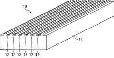
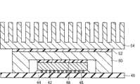
图1A、图1B是表示第一实施方式的碳纳米管板的结构的俯视图和概略剖视图。1A and 1B are plan views and schematic cross-sectional views showing the structure of a carbon nanotube sheet according to a first embodiment.
图2是表示第一实施方式的碳纳米管板的热导率与碳纳米管束的间隔的关系的曲线图。Fig. 2 is a graph showing the relationship between the thermal conductivity of the carbon nanotube sheet and the distance between carbon nanotube bundles in the first embodiment.
图3是说明第一实施方式的碳纳米管板的碳纳米管束的间隔的图。Fig. 3 is a diagram illustrating the spacing of carbon nanotube bundles in the carbon nanotube sheet according to the first embodiment.
图4A~图4E是表示第一实施方式的碳纳米管板的碳纳米管束的形状的俯视图。4A to 4E are plan views showing the shape of the carbon nanotube bundles of the carbon nanotube sheet according to the first embodiment.
图5A~图5D是表示第一实施方式的碳纳米管板的结构的概略剖视图。5A to 5D are schematic cross-sectional views showing the structure of the carbon nanotube sheet according to the first embodiment.
图6A~图6D是表示第一实施方式的碳纳米管板的制造方法的工序剖视图(其1)。6A to 6D are process cross-sectional views (Part 1) showing the method of manufacturing the carbon nanotube sheet according to the first embodiment.
图7A~图7D是表示第一实施方式的碳纳米管板的制造方法的工序剖视图(其2)。7A to 7D are process cross-sectional views (Part 2 ) showing the method of manufacturing the carbon nanotube sheet according to the first embodiment.
图8A、图8B是表示第二实施方式的碳纳米管板的结构的立体图和概略剖视图。8A and 8B are a perspective view and a schematic cross-sectional view showing the structure of a carbon nanotube sheet according to a second embodiment.
图9A~图9C是表示第二实施方式的碳纳米管板的制造方法的工序剖视图(其1)。9A to 9C are process cross-sectional views (Part 1) showing the method of manufacturing a carbon nanotube sheet according to the second embodiment.
图10A、图10B是表示第二实施方式的碳纳米管板的制造方法的工序剖视图(其2)。10A and 10B are process cross-sectional views (Part 2 ) showing the method of manufacturing a carbon nanotube sheet according to the second embodiment.
图11A、图11B是表示第二实施方式的碳纳米管板的制造方法的工序剖视图(其3)。11A and 11B are process cross-sectional views (Part 3 ) showing the method of manufacturing a carbon nanotube sheet according to the second embodiment.
图12A、图12B是表示第三实施方式的碳纳米管板的结构的立体图和概略剖视图。12A and 12B are a perspective view and a schematic cross-sectional view showing the structure of a carbon nanotube sheet according to a third embodiment.
图13A~图13C是表示第三实施方式的碳纳米管板的制造方法的工序剖视图(其1)。13A to 13C are process cross-sectional views (Part 1) showing the method of manufacturing a carbon nanotube sheet according to the third embodiment.
图14A~图14C是表示第三实施方式的碳纳米管板的制造方法的工序剖视图(其2)。14A to 14C are process cross-sectional views (Part 2 ) showing the method of manufacturing a carbon nanotube sheet according to the third embodiment.
图15A、图15B是表示第四实施方式的碳纳米管板的结构的俯视图和概略剖视图。15A and 15B are plan views and schematic cross-sectional views showing the structure of a carbon nanotube sheet according to a fourth embodiment.
图16是表示第四实施方式的碳纳米管板的结构的立体图。Fig. 16 is a perspective view showing the structure of a carbon nanotube sheet according to a fourth embodiment.
图17A~图17C是表示第四实施方式的碳纳米管板的制造方法的工序图(其1)。17A to 17C are process diagrams (Part 1) showing the method for producing a carbon nanotube sheet according to the fourth embodiment.
图18A、图18B是表示第四实施方式的碳纳米管板的制造方法的工序图(其2)。18A and 18B are process diagrams (Part 2 ) showing a method of manufacturing a carbon nanotube sheet according to a fourth embodiment.
图19A、图19B是表示第四实施方式的碳纳米管板的制造方法的工序图(其3)。19A and 19B are process diagrams (Part 3) showing the method for producing a carbon nanotube sheet according to the fourth embodiment.
图20是表示第四实施方式的碳纳米管板的结构的俯视图。Fig. 20 is a plan view showing the structure of a carbon nanotube sheet according to a fourth embodiment.
图21是表示第五实施方式的碳纳米管板的结构的俯视图。Fig. 21 is a plan view showing the structure of a carbon nanotube sheet according to a fifth embodiment.
图22A、图22B是表示第五实施方式的碳纳米管板的制造方法的工序图。22A and 22B are process diagrams showing a method of manufacturing a carbon nanotube sheet according to a fifth embodiment.
图23是表示第六实施方式的碳纳米管板的结构的概略剖视图。Fig. 23 is a schematic cross-sectional view showing the structure of a carbon nanotube sheet according to a sixth embodiment.
图24是表示第七实施方式的碳纳米管板的结构的概略剖视图。Fig. 24 is a schematic cross-sectional view showing the structure of a carbon nanotube sheet according to a seventh embodiment.
图25A~图25D是表示第七实施方式的碳纳米管板的制造方法的工序剖视图。25A to 25D are process cross-sectional views showing a method of manufacturing a carbon nanotube sheet according to a seventh embodiment.
图26是表示第八实施方式的电子设备的结构的概略剖视图。26 is a schematic cross-sectional view showing the structure of an electronic device according to an eighth embodiment.
图27是表示第九实施方式的电子设备的结构的概略剖视图。27 is a schematic cross-sectional view showing the structure of an electronic device according to a ninth embodiment.
图28是表示第十实施方式的电子设备的结构的立体图。28 is a perspective view showing the configuration of an electronic device according to a tenth embodiment.
具体实施方式Detailed ways
[第一实施方式][first embodiment]
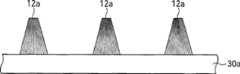
参照图1A至图7D说明第一实施方式的碳纳米管板及其制造方法。The carbon nanotube sheet and its manufacturing method of the first embodiment will be described with reference to FIGS. 1A to 7D .
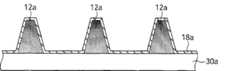
图1A、图1B是表示本实施方式的碳纳米管板的结构的俯视图和概略剖视图。图2是表示本实施方式的碳纳米管板的热导率和碳纳米管束的间隔的关系的曲线图。图3是说明本实施方式的碳纳米管板的碳纳米管束适宜的间隔的图。图4A~图4E是表示本实施方式的碳纳米管板的碳纳米管束的形状的俯视图。图5A~图5D是表示本实施方式的碳纳米管板的结构的概略剖视图。图6A~图6D和图7A~图7D是表示本实施方式的碳纳米管板的制造方法的工序剖视图。1A and 1B are a plan view and a schematic cross-sectional view showing the structure of a carbon nanotube sheet according to the present embodiment. Fig. 2 is a graph showing the relationship between the thermal conductivity of the carbon nanotube sheet and the spacing of the carbon nanotube bundles according to the present embodiment. Fig. 3 is a diagram illustrating an appropriate interval of carbon nanotube bundles in the carbon nanotube sheet according to the present embodiment. 4A to 4E are plan views showing the shape of the carbon nanotube bundles of the carbon nanotube sheet of the present embodiment. 5A to 5D are schematic cross-sectional views showing the structure of the carbon nanotube sheet of the present embodiment. FIGS. 6A to 6D and FIGS. 7A to 7D are cross-sectional views showing the steps of the method for manufacturing the carbon nanotube sheet according to the present embodiment.
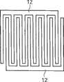
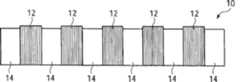
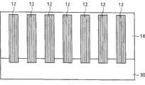
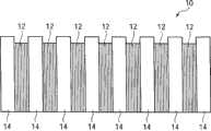
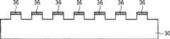
首先,参照图1A、图1B说明本实施方式的碳纳米管板的结构。图1A和图1B分别为表示本实施方式的碳纳米管板的结构的俯视图和剖视图。First, the structure of the carbon nanotube sheet of this embodiment will be described with reference to FIGS. 1A and 1B . 1A and 1B are a plan view and a cross-sectional view showing the structure of a carbon nanotube sheet according to this embodiment, respectively.
如图1A所示,本实施方式的碳纳米管板10具有如下结构:多个碳纳米管束12相互隔开间隔而配置,并且在其间隙中埋入形成有树脂材料等的填充层14。As shown in FIG. 1A , the
如图1B所示,各碳纳米管束12以在与板面垂直的方向上延伸的方式形成,并且具有定向在垂直于板面的方向上的多个碳纳米管。碳纳米管可以是单层碳纳米管或多层碳纳米管。考虑到散热性和导电性的要求,碳纳米管束12中所包括的碳纳米管的密度优选为1×10¹⁰根/cm2以上。As shown in FIG. 1B , each
碳纳米管束12的长度(板厚),由碳纳米管板10的用途确定而没有特别限定,优选可设定为5μm~500μm左右的值。The length (thickness) of the
在本实施方式的碳纳米管板10中,在碳纳米管束12之间设置有间隙,在该间隙中形成有填充层14。这是为了在碳纳米管之间形成填充层14时,提高填充材料的浸透性,并且抑制碳纳米管发生横倒等形状变化,从而保持碳纳米管原有保持的定向性(参照后述的制造方法)。In the
碳纳米管束12之间适宜的间隙根据形成填充层14的填充材料的粘度等而变化,因此无法一概确定,但是要求宽度远大于形成各碳纳米管束12的碳纳米管之间的间隙,优选设定为0.1μm~200μm左右的值。但是,碳纳米管束12的间隔越大,则板面内的碳纳米管的面密度越小,即作为板的热导率越低。另外,板面内的碳纳米管的面密度,也会因碳纳米管束12的尺寸而变化。因此,碳纳米管束12的间隔优选对应于板所要求的热导率,并且结合碳纳米管束12的尺寸来适当设定。The suitable gap between the carbon nanotube bundles 12 varies according to the viscosity of the filling material forming the
图2是表示板的热导率与碳纳米管束12的尺寸与间隔的关系的一个例子的曲线图。另外,图2所示的结果是在碳纳米管束12的形成区域具有将图1A所示的圆形排列成最密填充型的平面图案的情况下,在碳纳米管束12内的碳纳米管密度为1×10¹¹根/cm2,每根碳纳米管的热导率为1000W/m·K时计算出的。碳纳米管束(CNT束)12的尺寸以及间隔是指碳纳米管束12的形成区域的圆直径以及相邻的圆之间的最短距离。另外,图中虚线表示现有技术中使用的铟板的热导率。FIG. 2 is a graph showing an example of the relationship between the thermal conductivity of the plate and the size and spacing of the carbon nanotube bundles 12 . In addition, the result shown in FIG. 2 is the carbon nanotube density in the
如图2所示,碳纳米管板10的热导率主要取决于碳纳米管束12的尺寸和间隔,碳纳米管束12的尺寸越大,碳纳米管束12的间隔越小,则碳纳米管板10的热导率就越增大。As shown in Figure 2, the thermal conductivity of the
在图2的碳纳米管板10的情况下,为了得到与铟板同等以上的热导率(约80W/m·K)的碳纳米管板10,在CNT束的直径为50μm时,将CNT束的间隔设定为约4μm以下,在CNT束的直径为100μm时,将CNT束的间隔设定为约7μm以下,在CNT束的直径为200μm时,将CNT束的间隔设定为约14μm以下,在CNT束的直径为500μm时,将CNT束的间隔设定为约36μm以下,在CNT束的直径为1000μm时,将CNT束的间隔设定为约72μm以下,在CNT束的直径为2000μm时,将CNT束的间隔设定为约151μm以下。In the case of the
另一方面,在发热体为CPU等半导体晶片的情况下,当半导体晶片工作时并非整个晶片发热,而是以热点(发热源)为中心发热。如图3所示,在热点位于晶片20的表面附近时,若晶片20的厚度为T,则受到热点影响的晶片10背面的发热区域成为2T
各碳纳米管束12的平面形状不限于图1A所示的圆形。碳纳米管束12的平面形状除了圆形以外,例如可以使用三角形、四边形、六边形等多边形等。The planar shape of each
另外,多个碳纳米管束12的配置也不限于图1A所示的圆形的最密填充型排列。例如图4A和图4B所示,可以使碳纳米管束12分别配置在正方格子的各格子点上。另外,如图4C所示,也可以平面形状为三角形的碳纳米管束12改变上下朝向而按行排列。另外,如图4D所示,也可以使碳纳米管束12为条状图案。另外,如图4E所示,也可以使碳纳米管束12成为梳齿型图案。In addition, the arrangement of the plurality of carbon nanotube bundles 12 is not limited to the circular close-packed arrangement shown in FIG. 1A . For example, as shown in FIG. 4A and FIG. 4B , the carbon nanotube bundles 12 may be respectively arranged at grid points of a square grid. In addition, as shown in FIG. 4C , the carbon nanotube bundles 12 having a triangular planar shape may be arranged in rows with the vertical orientation changed. In addition, as shown in FIG. 4D, the carbon nanotube bundles 12 may be formed in a stripe pattern. In addition, as shown in FIG. 4E , the carbon nanotube bundles 12 may be formed into a comb-shaped pattern.
另外,本实施方式的碳纳米管板10的碳纳米管束12的上端和下端没有被填充层14覆盖。由此,当碳纳米管板10与散热体或发热体接触时,碳纳米管束12与散热体或发热体直接接触,因此能够大幅提高导热效率。In addition, the upper and lower ends of the carbon nanotube bundles 12 of the
另外,由于碳纳米管具有导电性,因此通过露出碳纳米管束12的上端和下端,从而能够将碳纳米管束12用作贯穿板的配线体。即,本实施方式的碳纳米管板10不仅是导热板,而且能够用作纵型配线板。In addition, since the carbon nanotubes have electrical conductivity, the carbon nanotube bundles 12 can be used as wiring bodies penetrating the plate by exposing the upper and lower ends of the carbon nanotube bundles 12 . That is, the
碳纳米管束12的高度和填充层14的厚度(均为板厚方向的长度)的关系,可以如图5A所示是相同的;或者如图5B所示,碳纳米管束12的一端部低于填充层14的表面;或者如图5C所示,碳纳米管束12的一端部突出于填充层14的表面。这些形状可以通过改变填充层14的材料或制造条件而制作出(参照后述的制造方法)。The relationship between the height of the
在将碳纳米管板10配置在散热体和发热体之间并被压接时,图5B的形状能够通过填充层14缓和施加在碳纳米管束12上的应力。另一方面,在图5C的形状中,能够提高碳纳米管束12对散热体和发热体的密接性,并且提高热导率。优选碳纳米管束12的高度与填充层14的厚度的关系,根据碳纳米管板10的使用目的或施加在板上的应力等适当设定。The shape of FIG. 5B can relax the stress applied to the carbon nanotube bundles 12 by the filling
另外,例如图5D所示,可以在碳纳米管板10的至少一个表面上,形成与碳纳米管束12的端部连接的覆膜18。覆膜18只要是热导率比填充层14的构成材料高的材料即可,并不特别限定。在碳纳米管板10用于导电用途时,可以采用具有导电性的材料,例如金属或合金等。覆膜18的构成材料例如能够采用铜(cu)、镍(Ni)、金(Au)等。另外,覆膜18不限于单层结构,例如也可以是钛(Ti)和金(Au)的层叠结构等2层或3层以上的层叠结构。In addition, as shown in FIG. 5D , for example, on at least one surface of the
覆膜18的膜厚没有特别限定。优选覆膜18的膜厚根据碳纳米管板10所要求的特性或覆膜18的构成材料来适当设定。The film thickness of the
通过设置热导性高的覆膜18,与没有设置覆膜18的情况相比,能够增加碳纳米管板10相对于被粘物(散热体、发热体)的接触面积。由此,能够降低碳纳米管束12与被粘物之间的接触热阻,从而提高碳纳米管板10的热导性。在碳纳米管板10用作导电板的情况下,能够提高导电性。By providing the
另外,在图5D中表示了在图5A的碳纳米管板10的一个表面上形成有覆膜18的情况,但是也可以在碳纳米管板10的两个面上形成覆膜18。另外,也可以在图5B或图5C所示的碳纳米管板10的一个表面或两个面上形成覆膜18。5D shows the case where the
填充层14的构成材料只要是在埋入碳纳米管时表现出液体状的性质而后固化的材料即可,并不特别限定。例如,作为有机类填充材料可以使用丙烯树脂、环氧树脂、硅树脂、聚酰亚胺树脂等。另外,作为无机类填充材料可以使用SOG(Spin On Glass:旋涂玻璃)等涂敷型绝缘膜形成用组合物等。另外,也可以采用铟、焊锡、金属焊料(例如银焊料)等金属材料。另外,可以采用例如聚苯胺、聚噻吩等导电性聚合物。The constituent material of the
另外,填充层14可以根据需要分散混合添加剂。例如可以使用导热性高的物质或导电性高的物质作为添加剂。通过在填充层14的部分中分散混合导热性的高添加剂,能够提高填充层14的部分的热导率,从而能够提高整个碳纳米管板的热导率。另外,在碳纳米管板用作导电板的情况下,在填充层14的部分中分散混合导电性高的添加剂。由此,能够提高填充层14的部分的电导率,从而提高整个碳纳米管板的电导率。在填充层14采用例如有机类填充材料等导热性低的绝缘材料时特别有效。作为导热性高的材料可以使用碳纳米管、金属材料、氮化铝、石英、氧化铝、石墨、巴基球(Buckminster-fullerene)等。作为导电性高的材料可以采用碳纳米管、金属材料等。In addition, the filling
上述的覆膜18在使碳纳米管板10的导热性或导电性提高,并且使用具有回流性的材料作为填充层14的构成材料时,还具有抑制碳纳米管束12变得凌乱的效果。The
下面参照图6A~图6D和图7~图7D对本实施方式的碳纳米管板的制造方法进行说明。Next, a method for manufacturing a carbon nanotube sheet according to this embodiment will be described with reference to FIGS. 6A to 6D and FIGS. 7 to 7D .
首先,准备用作形成碳纳米管板10用的基础的基板30(图6A))。作为基板30可以采用硅基板等半导体基板、氧化铝(蓝宝石)基板、MgO基板、玻璃基板等。另外,也可以在这些基板上形成薄膜。例如,可以在硅基板上形成膜厚300nm左右的硅氧化膜。First, a
基板30将在碳纳米管板10形成后被剥离。为此,优选基板30的至少与碳纳米管板10接触的面由易于从碳纳米管板10剥离的材料形成。或者,优选由相对于碳纳米管板10能够选择性地进行蚀刻的材料形成。The
例如,在填充层14的材料使用丙烯树脂的情况下,在基板30的表面形成与丙烯树脂粘接力弱的材料,例如硅氧化膜或硅氮化膜等。由此,能够容易地剥离碳纳米管板10。或者,基板30的表面由硅氧化膜或硅氮化膜等相对于碳纳米管板10能够选择性地进行蚀刻的材料形成。由此,通过蚀刻除去该膜,能够使碳纳米管板10与基板30分离。For example, when acrylic resin is used as the material of filling
接着,在基板30上通过旋涂法形成光致抗蚀剂膜32(图6B)。Next, a
接着,在光致抗蚀剂膜32上通过光刻法而形成使碳纳米管束12的形成预定区域露出的开口部34(图6C)。开口部34的图案例如采用图1A所示的图案,开口部34的直径(碳纳米管束12的形成区域的直径)为100μm,开口部34之间(碳纳米管束12之间)的间隙为20μm。另外,在光致抗蚀剂膜32上形成的开口部34的图案除了例如采用图1A所示的图案,还能够适用图4A~图4E所示的各种图案。Next, an
接着,例如通过溅涂法形成例如膜厚2.5nm的Fe(铁)膜,即形成Fe的催化剂金属膜36(图6D)。催化剂金属膜36形成在光致抗蚀剂膜32以及开口部34内的基板30上。Next, an Fe (iron) film having a film thickness of, for example, 2.5 nm, that is, a
催化剂金属除了Fe以外,也可以采用Co(钴)、Ni(镍)、Au(金)、Ag(银)、pt(白金)或者至少包括它们其中之一的材料的合金。另外,催化剂除了金属膜以外也可以采用微分型静电分级器(DMA:differentialmobility analyzer)等,也可以采用预先控制尺寸而制造的金属微粒子。此时,金属种类可以与薄膜的情况相同。As the catalyst metal other than Fe, Co (cobalt), Ni (nickel), Au (gold), Ag (silver), pt (platinum) or an alloy including at least one of them may be used. In addition, as the catalyst, a differential mobility analyzer (DMA: differential mobility analyzer) or the like may be used instead of a metal film, and metal fine particles manufactured by preliminarily controlling the size may be used. In this case, the metal type may be the same as in the thin film.
另外,这些催化剂金属的衬底膜可以是采用例如Mo(钼)、Ti(钛)、Hf(铪)、Zr(锆)、Nb(铌)、V(钒)、TaN(氮化钽)、TiSix(钛硅化合物)、Al(铝)、Al2O3(氧化铝)、TiOx(氧化钛)、Ta(钽)、W(钨)、Cu(铜)、Au(金)、Pt(白金)、Pd(钯)、TiN(氮化钛)等的膜或者由至少包括这些材料中一种材料的合金而形成的膜。例如可以采用Fe(2.5nm)/Al(10nm)的层叠结构、Co(2.6nm)/TiN(5nm)的层叠结构等。在使用金属微粒子的情况下,例如可以采用Co(平均直径:3.8nm)/TiN(5nm)等的层叠结构。In addition, the substrate film of these catalyst metals can be made of, for example, Mo (molybdenum), Ti (titanium), Hf (hafnium), Zr (zirconium), Nb (niobium), V (vanadium), TaN (tantalum nitride), TiSix (titanium silicon compound), Al (aluminum), Al2 O3 (aluminum oxide), TiOx (titanium oxide), Ta (tantalum), W (tungsten), Cu (copper), Au (gold), Pt (platinum ), Pd (palladium), TiN (titanium nitride) or the like, or a film formed of an alloy including at least one of these materials. For example, a stacked structure of Fe (2.5 nm)/Al (10 nm), a stacked structure of Co (2.6 nm)/TiN (5 nm), or the like can be employed. When metal fine particles are used, for example, a stacked structure of Co (average diameter: 3.8 nm)/TiN (5 nm) or the like can be employed.
接着,使光致抗蚀剂膜32上的催化剂金属膜36与光致抗蚀剂膜32一起进行分离(liftoff),在碳纳米管束12的形成预定区域的基板30上选择性地保留催化剂金属膜36(图7A)。Next, the
另外,虽然在上述例子中使用光刻法进行分离,由此在碳纳米管束12的形成预定区域上选择性地形成催化剂金属膜36,但是选择性地形成催化剂金属膜36的方法不限于此。例如可以采用在碳纳米管束12的形成预定区域上具有开口部的金属掩模。在通过该金属掩模来覆盖基板30的表面的状态下,溅涂催化剂金属,由此能够在碳纳米管束12的形成预定区域上选择性地形成催化剂金属膜36。In addition, although the
接着,在基板30上例如通过热丝(hot filament)CVD法以催化剂金属膜36为催化剂生成碳纳米管。碳纳米管的生长条件是例如采用乙炔和氩气的混合气(分压比1:9)为原料气体,成膜室内的总气压为1kPa,热丝温度为1000℃,生长时间为20分钟。由此,能够形成层数为3到6层(平均4层左右),直径为4~8nm(平均6nm),长度80μm(生长率:4μm/min)的多层碳纳米管。另外,碳纳米管也可以通过热CVD法或远程等离子(remoteplasma)CVD法等其它成膜方法来形成。另外,生长的碳纳米管也可以是单层碳纳米管。另外,炭元素原料除了乙炔外,也可以采用甲烷、乙烯等碳氢化合物,或乙醇、甲醇等醇类等。Next, carbon nanotubes are formed on the
这样,在基板30的形成有催化剂金属膜36的区域上,选择性地形成有碳纳米管束12,所述碳纳米管束12具有定向在基板30的法线方向上(垂直定向)的多个碳纳米管(图7B)。另外,在以上述生长条件形成的碳纳米管束12中,碳纳米管束12内的碳纳米管密度为1×10¹¹根/cm2左右。In this way, on the region of the
接着,通过例如旋涂法来涂敷成为填充层14的填充材料。此时对涂敷溶液的粘度和旋涂机的转速进行适当设定,以避免填充材料覆盖到碳纳米管束12上。Next, a filling material to be the filling
例如在填充材料使用丙烯树脂的情况下,为了使碳纳米管束12的高度和填充层14的厚度基本相同(参照图5A),例如可以通过在2000rpm,20秒期间的条件下涂敷粘度为440mPa·s的丙烯树脂来实现。For example, in the case of using acrylic resin as the filling material, in order to make the height of the carbon nanotube bundles 12 substantially the same as the thickness of the filling layer 14 (see FIG. · s acrylic resin to achieve.
另外,为了使填充层14比碳纳米管束12的高度薄(参照图5C),例如可以通过在4000rpm,20秒期间的条件下涂敷粘度为440mPa·S的丙烯树脂来实现。或者,通过在2000rpm,20秒期间的条件下涂敷用MEK(丁酮)溶液稀释为80w%的丙烯树脂来实现。In addition, in order to make the filled
在以覆盖在碳纳米管束12上的方式形成填充材料后,可以通过灰化(ashing)等使碳纳米管束12的上表面露出(参照第二实施方式)。After the filler is formed so as to cover the carbon nanotube bundles 12, the upper surface of the carbon nanotube bundles 12 may be exposed by ashing or the like (see the second embodiment).
填充材料只要是表现出液体状的性质而后能够固化的材料即可,并不特别限定。例如作为有机类填充材料可以采用丙烯树脂、环氧树脂、硅树脂、聚酰亚胺树脂等。另外,作为无机类填充材料可以采用SOG等涂敷型绝缘膜形成用组合物等。另外,也可以采用铟、焊锡、金属焊料(例如银焊料)等金属材料。另外,例如也可以采用例如聚苯胺、聚噻吩等导电性聚合物。The filler is not particularly limited as long as it exhibits liquid properties and can be cured thereafter. For example, acrylic resin, epoxy resin, silicone resin, polyimide resin, etc. can be used as an organic filler. In addition, as the inorganic filler, a coating-type insulating film-forming composition such as SOG or the like can be used. In addition, metal materials such as indium, solder, and metal solder (eg, silver solder) can also be used. In addition, for example, conductive polymers such as polyaniline and polythiophene can also be used.
在形成填充层14时,由于在基板30上隔开间隔形成多个碳纳米管束12,因此涂敷的填充材料首先沿着该间隙在整个基板30的表面上扩展。然后,填充材料逐渐渗透到碳纳米管束12内。When forming the
若在基板的整个表面上形成碳纳米管,则在填充材料浸透到碳纳米管束内时,每一根碳纳米管彼此聚集起来,从而碳纳米管束失去原有保持的定向性,例如发生横倒等变形。If carbon nanotubes are formed on the entire surface of the substrate, when the filler material penetrates into the carbon nanotube bundles, each carbon nanotube is aggregated with each other, so that the carbon nanotube bundles lose their original orientation, such as falling sideways. Wait for deformation.
但是,通过如本实施方式那样在碳纳米管束12之间设置间隙,填充材料在基板30的整个表面上扩展后,逐渐浸透到碳纳米管束12内。因此,先填充到碳纳米管束12之间的填充材料在填充材料浸透到碳纳米管束内时,作为保持碳纳米管形状的支撑部发挥作用,从而能够抑制碳纳米管束12的形状变化。由此,能够在保持碳纳米管束12的定向方向的情况下形成填充层14。However, by providing gaps between the carbon nanotube bundles 12 as in the present embodiment, the filler spreads over the entire surface of the
碳纳米管束12之间的适宜的间隙根据填充材料的种类和粘度等而变化,无法一概确定。经过本发明人等研究发现,通过隔开0.1μm以上的间隔,能够防止碳纳米管束的形状变化。The appropriate gap between the carbon nanotube bundles 12 varies depending on the type and viscosity of the filler, and cannot be determined uniformly. The inventors of the present invention have found that the shape change of the carbon nanotube bundles can be prevented by creating an interval of 0.1 μm or more.
另外,树脂层14也可以通过在填充材料的溶液中浸泡基板30来形成(所谓浸泡法)。此时也能够通过在碳纳米管束12之间设置的间隙来防止碳纳米管束的形状变化。In addition, the
接着,填充材料固化而形成填充材料的填充层14(图7C)。例如,在填充材料使用丙烯树脂等光固化性材料的情况下,能够通过光照射使填充材料固化。另外,在填充材料使用环氧树脂或硅类树脂等热固化性材料的情况下,能够通过热处理使填充材料固化。在环氧树脂的情况下,例如能够通过150℃,1小时的热处理进行热固化。另外,在硅类树脂的情况下,例如可以通过该200℃,1小时的热处理进行热固化。Next, the filling material is cured to form a
另外,在填充层14固化后碳纳米管束12的上端部没有充分露出或被填充层14覆盖的情况下,可以通过化学机械抛光(CMP:Chemical MechanicalPolishing)或氧等离子灰化,将碳纳米管束12上的填充层14除去。In addition, when the upper end of the
接着,将碳纳米管束12和树脂层14从基板30剥离,从而得到碳纳米管板10(图7D)。Next, the
此时,在基板30的表面由易于剥离碳纳米管板10的材料形成的情况下,易于从碳纳米管板10剥离基板30。例如是在基板30的表面上形成硅氧化膜或硅氮化膜,并通过丙烯树脂形成填充层14的情况等。At this time, when the surface of the
或者,在基板30表面形成不易剥离碳纳米管板10但是相对于碳纳米管板10能够选择性除去的层的情况下,能够通过选择性地除去该层来剥离基板30。例如是在基板30的表面上形成硅氧化膜或硅氮化膜,通过环氧树脂形成填充层14的情况等。该硅氧化膜或硅氮化膜是通过使用氟酸水溶液或热磷酸等进行的湿式蚀刻而除去的,由此能够使碳纳米管板10从基板30分离。Alternatively, when a layer that is difficult to peel off the
在基板30的表面由不易剥离碳纳米管板10并且无法进行选择性除去的材料形成的情况下,可以通过锋利的刀具使碳纳米管板10从基板30剥离。例如是基板30为蓝宝石基板而填充层14由硅类树脂形成的情况。通过在基板30和碳纳米管板10之间插入锋利的刀具,能够将碳纳米管板10从基板30剥离。When the surface of the
由于在剥离前碳纳米管束12直接与基板30接触,因此在剥离后的碳纳米管板10的位于基板30一侧的表面上露出碳纳米管束12。因此,在通过上述制造方法而形成的碳纳米管板10中,能够使碳纳米管束12从板的两个面露出。Since the carbon nanotube bundles 12 directly contact the
另外,在填充材料使用丙烯树脂的情况下,在丙烯树脂固化的過程中,因为填充材料和碳纳米管的体积收缩率不同,所以碳纳米管束12的部分相对地降低。即,在碳纳米管板10的与基板30接触一侧的表面上,碳纳米管束12的端部成为低于填充层14的表面的形状(参照图5B)。该凹处可用于缓和板的热膨胀应力,并且具有提高密接性的效果。In addition, when acrylic resin is used as the filler, during the curing of the acrylic resin, the volume shrinkage ratio of the filler and the carbon nanotubes is different, so that the portion of the carbon nanotube bundles 12 is relatively reduced. That is, on the surface of the
然后,根据需要在碳纳米管板10的一个面或两个面上形成覆膜18(参照图5D)。覆膜18例如可以通过溅涂法形成。可以采用例如膜厚10nm的钛(Ti)膜和例如膜厚50nm的金(Au)膜的层叠膜作为覆膜18。Then, coating
这样,根据本实施方式,在基板上形成彼此分离的多个碳纳米管束后,填充填充材料来形成保持碳纳米管束的填充层,因此能够防止在填充层时碳纳米管束形状发生变化。由此,能够易于形成碳纳米管束定向在板的膜厚方向上的碳纳米管板。另外,碳纳米管束的两端部能够从填充层露出,因此能够提高对被粘物的导热性和电导率。Thus, according to the present embodiment, after forming a plurality of separated carbon nanotube bundles on the substrate, the filling material is filled to form a filled layer holding the carbon nanotube bundles, so that the shape of the carbon nanotube bundles can be prevented from changing when the layer is filled. This makes it possible to easily form a carbon nanotube sheet in which carbon nanotube bundles are oriented in the film thickness direction of the sheet. In addition, since both ends of the carbon nanotube bundles can be exposed from the filled layer, thermal conductivity and electrical conductivity to the adherend can be improved.
[第二实施方式][Second Embodiment]
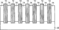
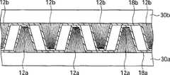
参照图8A至图11B说明第二实施方式的碳纳米管板及其制造方法。另外,对于和图1A至图7D所示第一实施方式的碳纳米管板及其制造方法相同的结构要素标记相同的附图标记且省略或简化说明。A carbon nanotube sheet and its manufacturing method according to the second embodiment will be described with reference to FIGS. 8A to 11B . In addition, the same reference numerals are assigned to the same structural elements as those of the carbon nanotube sheet and its manufacturing method according to the first embodiment shown in FIGS. 1A to 7D , and descriptions thereof are omitted or simplified.
图8A、图8B是表示本实施方式的碳纳米管板的结构的立体图和概略剖视图。图9A至图11B是表示本实施方式的碳纳米管板的制造方法的工序剖视图。8A and 8B are a perspective view and a schematic cross-sectional view showing the structure of a carbon nanotube sheet according to this embodiment. 9A to 11B are cross-sectional views showing the steps of the method for manufacturing the carbon nanotube sheet according to the present embodiment.
首先,参照图8A、图8B说明本实施方式的碳纳米管板的结构。图8A和图8B分别是表示本实施方式的碳纳米管板的结构的立体图和剖视图。First, the structure of the carbon nanotube sheet of this embodiment will be described with reference to FIGS. 8A and 8B . 8A and 8B are a perspective view and a cross-sectional view showing the structure of a carbon nanotube sheet according to this embodiment, respectively.
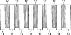
如图8A所示,本实施方式的碳纳米管板10是由填充层14埋入具有条状图案的碳纳米管束12而构成的。另外,如图8B所示,碳纳米管束12的端部位置在板的两个面上比填充层14的表面高。As shown in FIG. 8A , the
通过形成这种碳纳米管板10,在该板与散热体或发热体接触时,能够容易且可靠地使碳纳米管束12与散热体或发热体连接,从而能够大幅提高导热效率。在碳纳米管板10用作导电性板的情况下,能够容易且可靠地与其它配线结构体连接,从而能够大幅降低接触电阻。By forming such a
另外,若在本实施方式的碳纳米管板10所连接的其它结构体的表面上,形成有与本实施方式的碳纳米管板10的表面凹凸嵌合的表面凹凸,则能够通过彼此凹凸的啮合而获得密接性较高的连接。本实施方式的碳纳米管板10所具有的条状的凹凸图案等是适于此目的的图案。In addition, if the surface of the other structure to which the
考虑到可靠地与其它结构体连接,碳纳米管束12相对于填充层14的突出量约为1μm以下(例如500nm左右)即可。根据后述的本实施方式的制造方法,能够容易地控制碳纳米管束12的突出量。In consideration of reliable connection with other structures, the amount of protrusion of the carbon nanotube bundles 12 relative to the
另外,在图8A、图8B的例子中,在板的两个面,使碳纳米管束12的端部从填充层14的表面突出,但是也可以仅在板的一个表面上形成这种结构。碳纳米管束12的平面图案、填充层14的构成材料、碳纳米管束12和填充层14的制造条件以及膜厚等其它物理性质值等与第一实施方式的碳纳米管板的情况相同。In addition, in the example of FIG. 8A and FIG. 8B, the ends of the carbon nanotube bundles 12 protrude from the surface of the
接着,参照图9A至图11B说明本实施方式的碳纳米管板的制造方法。另外,本实施方式的碳纳米管板的具体制造条件与第一实施方式的情况相同。Next, a method for manufacturing the carbon nanotube sheet of the present embodiment will be described with reference to FIGS. 9A to 11B . In addition, the specific production conditions of the carbon nanotube sheet of this embodiment are the same as those of the first embodiment.
首先,准备用作形成碳纳米管板10用的基础的基板30。作为基板30例如可以采用在硅基板上形成膜厚1μm左右的硅氧化膜的结构。First, a
接着,在基板30上通过光刻法形成光致抗蚀剂膜32,所述光致抗蚀剂膜32具有使碳纳米管束12的形成预定区域露出的开口部34。Next, a
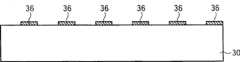
接着,以光致抗蚀剂膜32为掩模对基板30进行各向异性蚀刻,从而在基板30的表面上形成深度500nm左右的凹部38(图9A)。凹部38形成在基板30的碳纳米管束12形成预定区域上。另外,凹部38的宽度例如能够设定为100μm,凹部38的间隔例如能够设定为20μm。优选凹部38的宽度和间隔根据碳纳米管板10所要求的热导率等进行适当设定。Next, the
凹部38的深度与碳纳米管束12相对于填充层14的突出量相对应。因此,通过适当设定凹部38的深度,能够控制碳纳米管束12相对于填充层14的突出量。The depth of the
接着,例如通过溅涂法形成例如膜厚2.5nm的Fe(铁)膜,从而形成Fe的催化剂金属膜36(图9B)。催化剂金属膜36形成在光致抗蚀剂膜32上和基板30的凹部38内。Next, an Fe (iron) film having a film thickness of, for example, 2.5 nm is formed by, for example, sputtering to form a Fe catalyst metal film 36 ( FIG. 9B ). A
接着,使光致抗蚀剂膜32上的催化剂金属膜36与光致抗蚀剂膜32一起分离,在基板30的凹部38内选择性地保留催化剂金属膜36(图9C)。Next, the
接着,在基板30上例如通过热丝CVD法以催化剂金属膜36为催化剂生成碳纳米管。由此,在基板30的凹部38形成区域上,选择性地形成碳纳米管束12,所述碳纳米管束12具有定向在基板30的法线方向上的多个碳纳米管(图10A)。Next, carbon nanotubes are formed on the
接着,在例如通过旋涂法涂敷例如环氧树脂后,进行例如150℃,1小时的热处理,从而使环氧树脂固化。由此,形成环氧树脂的填充层14(10B)。Next, after applying, for example, an epoxy resin by, for example, spin coating, heat treatment is performed at, for example, 150° C. for 1 hour to cure the epoxy resin. In this way, epoxy resin filling layer 14 ( 10B) is formed.
接着,例如使用氧等离子进行灰化,从而将填充层14的上部除去,使碳纳米管束12的上端部露出(图11A)。灰化条件例如可以是功率200W、时间10分钟。也可以通过在氧环境中加热来除去填充层14的上部,以代替使用氧等离子的灰化。Next, ashing is performed using, for example, oxygen plasma to remove the upper portion of the
在填充层14使用环氧树脂的情况下,填充层14相对于碳纳米管束12的选择比为1.26左右。因此,通过从填充层14上部进行灰化,能够使碳纳米管束12的上端部的高度比填充层14的表面高。另外,通过适当设定填充层14的蚀刻量,能够控制碳纳米管束12相对于填充层14的突出量。When epoxy resin is used for the filled
在使用氧等离子进行灰化前,例如也可以通过化学机械抛光使碳纳米管束12的上端部露出。Before ashing with oxygen plasma, the upper ends of the carbon nanotube bundles 12 may be exposed, for example, by chemical mechanical polishing.
另外,虽然在本实施方式中以覆盖碳纳米管束12的上端部的方式形成填充层14,但是也可以如第一实施方式那样对填充层14的涂敷条件进行控制,使碳纳米管束12的上端部露出。此时,不需要图11A的工序。另外,在仅在板的一面使碳纳米管束12的端部从填充层14的表面突出的情况下,在图11A的工序中,仅使碳纳米管束12的上端部露出即可。In addition, although the
接着,将碳纳米管束12和树脂层14从基板30剥离,从而能够得到在板的两个面上碳纳米管束12从填充层14的表面突出的碳纳米管板10(图11B)。Next, carbon nanotube bundles 12 and
这样,根据本实施方式,能够易于形成碳纳米管束的端部突出于填充层的表面的碳纳米管板。由此,能够进一步提高相对于被粘物的热导率和电导率。Thus, according to the present embodiment, it is possible to easily form a carbon nanotube sheet in which the ends of the carbon nanotube bundles protrude from the surface of the filled layer. Thereby, thermal conductivity and electrical conductivity with respect to an adherend can be further improved.
[第三实施方式][Third Embodiment]
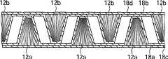
参照图12A至图14C说明第三实施方式的碳纳米管板及其制造方法。另外,对于和图1A至图11B所示第一和第二实施方式的碳纳米管板及其制造方法相同的结构要素标记相同的附图标记,且省略或简化说明。A carbon nanotube sheet and its manufacturing method according to a third embodiment will be described with reference to FIGS. 12A to 14C . In addition, the same reference numerals are assigned to the same constituent elements as those of the carbon nanotube sheet and the method of manufacturing the same according to the first and second embodiments shown in FIGS. 1A to 11B , and descriptions are omitted or simplified.
图12A、图12B是表示本实施方式的碳纳米管板的结构的立体图和概略剖视图。图13A~图13C和图14A~图14C是表示本实施方式的碳纳米管板的制造方法的工序剖视图。12A and 12B are a perspective view and a schematic cross-sectional view showing the structure of a carbon nanotube sheet according to this embodiment. FIGS. 13A to 13C and FIGS. 14A to 14C are cross-sectional views showing the steps of the method for manufacturing the carbon nanotube sheet according to the present embodiment.
首先,参照图12、图12B说明本实施方式的碳纳米管板的结构。图12A和图12B分别是表示本实施方式的碳纳米管板的结构的立体图和剖视图。First, the structure of the carbon nanotube sheet of the present embodiment will be described with reference to FIGS. 12 and 12B. 12A and 12B are a perspective view and a cross-sectional view showing the structure of a carbon nanotube sheet according to this embodiment, respectively.
如图12A所示,本实施方式的碳纳米管板10是由填充层14埋入具有条状图案的碳纳米管束12而构成的。另外,如图12B所示,碳纳米管束12的端部位置在板的一个面上比填充层14的表面低。碳纳米管束12的端部没有被填充层14覆盖。As shown in FIG. 12A , the
通过形成这种碳纳米管板10,在使碳纳米管板10与散热体或发热体接触时,能够使碳纳米管束12与散热体或发热体直接连接,从而能够大幅提高导热效率。另外,在碳纳米管板10用作导电性板的情况下,能够与其它配线结构体直接连接,从而能够大幅降低接触电阻。另外,如第一实施方式所述那样,在将碳纳米管板10配置于散热体和发热体之间并进行压接时,能够通过填充层14缓和施加在碳纳米管束12上的应力。By forming such a
另外,若在本实施方式的碳纳米管板10所连接的其它结构体的表面上,形成与本实施方式的碳纳米管板10的表面凹凸嵌合的表面凹凸,则能够通过彼此凹凸的啮合而获得密接性高的连接。本实施方式的碳纳米管板10所具有的条状凹凸图案等是适于此目的的图案。In addition, if on the surface of other structures to which the
碳纳米管束12的平面图案、填充层14的构成材料、碳纳米管束12和填充层14的制造条件以及膜厚等其它物理性质值等,与第一实施方式的碳纳米管板的情况相同。The planar pattern of the
接着,参照图13~图13C和图14A~图14C说明本实施方式的碳纳米管板的制造方法。另外,本实施方式的碳纳米管板的具体制造条件与第一实施方式的情况相同。Next, a method for manufacturing the carbon nanotube sheet of the present embodiment will be described with reference to FIGS. 13 to 13C and 14A to 14C. In addition, the specific production conditions of the carbon nanotube sheet of this embodiment are the same as those of the first embodiment.
首先,准备用作形成碳纳米管板10用的基础的基板30。作为基板30例如采用在硅基板上形成膜厚1μm左右的硅氧化膜的结构。First, a
接着,在基板30上例如通过溅涂法形成例如膜厚2.5nm的Fe(铁)膜,从而形成Fe的催化剂金属膜36(图13A)。Next, an Fe (iron) film having a film thickness of 2.5 nm is formed on the
接着,在基板30上通过光刻法形成光致抗蚀剂膜32,所述光致抗蚀剂膜32具有覆盖碳纳米管束12的形成预定区域且露出其它区域的开口部34。Next, a
接着,以光致抗蚀剂膜32为掩模对催化剂金属膜36和基板30进行各向异性蚀刻,从而在基板30的表面上形成深度500nm左右的凹部38(图13B)。凹部38形成在基板30的碳纳米管束12形成预定区域以外的区域上。另外,凹部38的宽度例如能够设定为20μm,凹部38的间隔例如能够设定为100μm。凹部38的宽度和间隔根据碳纳米管板10所要求的热导率等进行适当设定。Next, the
接着,例如通过灰化来除去光致抗蚀剂膜32(图13C)。Next, the
接着,在基板30上例如通过热丝CVD法以催化剂金属膜36为催化剂来生成碳纳米管。由此,在基板30的凹部38形成区域以外的区域上,选择性地形成碳纳米管束12,所述碳纳米管束12具有定向在基板30的法线方向上的多个碳纳米管(图14A)。Next, carbon nanotubes are formed on the
接着,在例如通过旋涂法涂敷环氧树脂后,进行例如150℃,1小时的热处理,从而使环氧树脂固化。由此,形成环氧树脂的填充层14。填充层14也可以形成在基板30的凹部38内(图14B)。Next, after applying an epoxy resin by, for example, a spin coating method, heat treatment is performed, for example, at 150° C. for 1 hour to cure the epoxy resin. Thus, the filled
另外,虽然在图14B中示出了将碳纳米管束12的表面和填充层14的表面平坦处理后的情况,但是碳纳米管束12的端部也可以从填充层14的表面突出。分别制作这些形状的方法与第一和第二实施方式的情况相同。In addition, although the surface of the
接着,将碳纳米管束12和树脂层14从基板30剥离,从而得到在板的一个面上碳纳米管束12的端部位置比填充层14的表面低的碳纳米管板10(图14C)。Next, the carbon nanotube bundles 12 and the
这样,根据本实施方式,能够易于形成碳纳米管束的端部低于填充层的表面的碳纳米管板。由此,在将碳纳米管板压接在被粘物上时,能够通过填充层缓和施加在碳纳米管束上的应力。Thus, according to the present embodiment, it is possible to easily form a carbon nanotube sheet in which the ends of the carbon nanotube bundles are lower than the surface of the filled layer. Thereby, when the carbon nanotube sheet is pressure-bonded to the adherend, the stress applied to the carbon nanotube bundle can be relieved by the filling layer.
[第四实施方式][Fourth Embodiment]
参照图15A至图19B说明第四实施方式的碳纳米管板及其制造方法。另外,对于和图1A至图14C所示第一至第三实施方式的碳纳米管板及其制造方法相同的结构要素标记相同的附图标记,且省略或简化说明。A carbon nanotube sheet and its manufacturing method according to a fourth embodiment will be described with reference to FIGS. 15A to 19B . In addition, the same reference numerals are assigned to the same structural elements as those of the carbon nanotube sheet and the manufacturing method thereof according to the first to third embodiments shown in FIGS. 1A to 14C , and descriptions are omitted or simplified.
图15A、图15B是表示本实施方式的碳纳米管板的结构的俯视图和概略剖视图。图16是表示本实施方式的碳纳米管板的结构的立体图。图17A至图19B是表示本实施方式的碳纳米管板的制造方法的工序图。15A and 15B are plan views and schematic cross-sectional views showing the structure of a carbon nanotube sheet according to the present embodiment. Fig. 16 is a perspective view showing the structure of the carbon nanotube sheet of the present embodiment. 17A to 19B are process diagrams showing a method of manufacturing a carbon nanotube sheet according to this embodiment.
首先参照图15、图15B和图16说明本实施方式的碳纳米管板的结构。图15A和图15B分别是表示本实施方式的碳纳米管板的结构的俯视图和剖视图。First, the structure of the carbon nanotube sheet of the present embodiment will be described with reference to FIGS. 15 , 15B, and 16 . 15A and 15B are a plan view and a cross-sectional view showing the structure of a carbon nanotube sheet according to this embodiment, respectively.
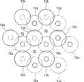
如图15、图15B和图16所示,本实施方式的碳纳米管板10具有如下结构:将多个碳纳米管束12a、12b隔开间隔进行配置,并在该间隙中埋入树脂材料等的填充层14,在这点上与第一至第三实施方式的碳纳米管板是相同的。As shown in FIG. 15, FIG. 15B, and FIG. 16, the
在本实施方式的碳纳米管板10中,多个碳纳米管束12分别具有一个端部的直径比另一端部的直径小的锥状。各碳纳米管束12a、12b从直径大的端部一侧朝向直径小的端部一侧,碳纳米管之间的间隔逐渐减小而成为锥状。换而言之,在碳纳米管束12a、12b的直径大的端部一侧和直径小的端部一侧,碳纳米管根数实质上没有变化。In the
多个碳纳米管束12分为两组,一组是在碳纳米管板10的一个表面一侧直径小的碳纳米管束12a,一组是在碳纳米管板10的另一表面一侧直径小的碳纳米管束12b。碳纳米管束12a与碳纳米管束12b,例如图15B和图16所示以彼此嵌合且埋入彼此的间隙之中的方式而配置。A plurality of carbon nanotube bundles 12 are divided into two groups, one group is a
若从一个表面一侧看碳纳米管板10,则例如图15A和图15B所示,碳纳米管束12a的直径小的端部和碳纳米管束12b的直径大的端部露出。在碳纳米管板10的另一表面一侧,如图15B所示,碳纳米管束12a的直径大的端部和碳纳米管束12b的直径小的端部露出。When the
通过采用这样的碳纳米管束12a、12b,能够提高碳纳米管板10的单位面积的碳纳米管的根数(碳纳米管的面密度)。By using such carbon nanotube bundles 12 a and 12 b , the number of carbon nanotubes per unit area of the carbon nanotube sheet 10 (surface density of carbon nanotubes) can be increased.
例如,可以考虑到碳纳米管束12b直径大的端部的直径和配置间隔与图1A所示第一实施方式的碳纳米管板的碳纳米管束12相同的情况。此时,如图15A所示,能够在碳纳米管束12b的间隙中再配置相同根数的碳纳米管束12a。即,能够使碳纳米管板10的碳纳米管的面密度加倍。由此,能够大幅提高碳纳米管板10的导热性和导电性。For example, it is conceivable that the diameter and arrangement interval of the large-diameter ends of the carbon nanotube bundles 12b are the same as those of the carbon nanotube bundles 12 of the carbon nanotube sheet of the first embodiment shown in FIG. 1A. At this time, as shown in FIG. 15A , the same number of carbon nanotube bundles 12 a can be further arranged in the gaps between the carbon nanotube bundles 12 b. That is, the areal density of carbon nanotubes in the
接着,参照图17A至图19B说明本实施方式的碳纳米管板的制造方法。Next, a method for manufacturing the carbon nanotube sheet of the present embodiment will be described with reference to FIGS. 17A to 19B .
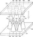
首先,例如与第一实施方式的碳纳米管板的制造方法相同,在碳纳米管束12的形成预定区域的基板30a上,选择性地形成催化剂金属膜36(图17A)。基板30a与第一至第三实施方式的基板30相同。First, for example, a
接着,在基板30a上,通过例如热丝CVD法以催化剂金属膜36为催化剂来生成碳纳米管。由此,在基板30a的形成有催化剂金属膜36的区域上,选择性地形成碳纳米管束12,所述碳纳米管束12具有定向在基板30a的法线方向上的多个碳纳米管(图17B)。Next, carbon nanotubes are formed on the
接着,将形成了碳纳米管束12的基板30a浸泡在液体中,然后进行干燥。若将碳纳米管束12浸泡到液体中,则碳纳米管的间隙会充满液体。若在该状态下将液体蒸发,则碳纳米管之间的液体体积减小,同时由于表面张力而在邻接的碳纳米管之间产生引力。基板30a一侧的碳纳米管束12的端部固定在基板30a上,因此碳纳米管之间的间隔不变。另一方面,碳纳米管的前端没有固定,因此碳纳米管之间的间隔逐渐变窄。当碳纳米管之间的间隙足够小时,碳纳米管彼此间由于范德瓦尔斯力而固定。由此,对液体进行干燥后的碳纳米管束12成为前端部直径小于基板30a一侧直径的锥状的碳纳米管束12a(图17C)。Next, the
使碳纳米管束12成为锥状时采用的液体只要对碳纳米管浸润性高,并且能够在不损坏碳纳米管的高温下也进行蒸发的液体即可,并不特别限定。例如适于使用醇类药液或酮类药液等有机药液。醇类药液没有特别限定,例如可以是异丙醇、乙醇、甲醇等。另外,酮类药液没有特别限定,例如可以是丙酮、丁酮、甲基异丁基酮等。The liquid used for forming the
接着,与图17A至图17C所示工序相同,在基板30b上形成锥状的碳纳米管束12b。Next, the tapered carbon nanotube bundles 12b are formed on the
接着,以基板30a的形成有碳纳米管束12a的面,与基板30b的形成有碳纳米管束12b的面相对的方式,使基板30a与基板30贴合(图18A~图18B)。Next, the
此时,以使碳纳米管束12a与碳纳米管束12b彼此嵌合且埋入彼此的间隙之中的方式,来布局碳纳米管束12a、12b。由此,碳纳米管束12a之间的间隙和碳纳米管束12b的间隙被彼此填充。另外,碳纳米管束12a的前端与基板30b的表面接触,碳纳米管束12b的前端与基板30a的表面接触。At this time, the
另外,碳纳米管束12a、12b的配置区域只要是埋入彼此的间隙之中的关系就不限于本实施方式而可以适当变更。碳纳米管束12a的形成区域的形状和尺寸可以与碳纳米管束12b的形成区域的形状和尺寸不同,碳纳米管束12a与碳纳米管束12b的相互之间的排列也可以不同。In addition, the arrangement regions of the
接着,通过例如灌注法将构成填充层14的填充材料埋设在基板30a和基板30之间,并且使填充层14埋入碳纳米管束12a、12b之间(图19A)。此时,碳纳米管束12a、12b的端部与基板30a、30b直接接触,因此碳纳米管束12a、12b的端部不会被填充层14覆盖。在防止碳纳米管聚集的效果方面与第一实施方式的情况相同。Next, a filling material constituting filling
接着,例如与第一实施方式的碳纳米管板的制造方法相同,将碳纳米管束12a、12b和填充层14从基板30a、30b剥离,从而得到碳纳米管板10(图19B)。Next, for example, the
接着,根据需要进行填充层14的回蚀(etch back)等,使碳纳米管束12a、12的端部从填充层14的表面突出。Next, if necessary, etch back of the filled
这样,根据本实施方式,形成了具有一面一侧的直径小的碳纳米管束和另一面一侧的直径小的碳纳米管束的碳纳米管板,因此能够大幅增加碳纳米管的面密度。由此,能够大幅提高碳纳米管板的导热性以及/或者导电性。In this way, according to the present embodiment, a carbon nanotube sheet having small-diameter carbon nanotube bundles on one side and small-diameter carbon nanotube bundles on the other side is formed, so that the areal density of carbon nanotubes can be greatly increased. Thereby, the thermal conductivity and/or electrical conductivity of the carbon nanotube sheet can be greatly improved.
[第五实施方式][Fifth Embodiment]
参照图20至图22B说明第五实施方式的碳纳米管板及其制造方法。另外,对于和图1A至图19B所示第一至第四实施方式的碳纳米管板及其制造方法相同的结构要素标记相同的附图标记,且省略或简化说明。A carbon nanotube sheet and its manufacturing method according to a fifth embodiment will be described with reference to FIGS. 20 to 22B. In addition, the same reference numerals are assigned to the same structural elements as those of the carbon nanotube sheet and the manufacturing method thereof according to the first to fourth embodiments shown in FIGS. 1A to 19B , and descriptions are omitted or simplified.
图20是表示第四实施方式的碳纳米管板的结构的俯视图。图21是表示本实施方式的碳纳米管板的结构的俯视图。图22A、图22B是表示本实施方式的碳纳米管板的制造方法的工序图。Fig. 20 is a plan view showing the structure of a carbon nanotube sheet according to a fourth embodiment. Fig. 21 is a plan view showing the structure of the carbon nanotube sheet of the present embodiment. 22A and 22B are process diagrams showing a method for producing a carbon nanotube sheet according to this embodiment.
在第四实施方式的碳纳米管板及其制造方法中,通过贴合两个基板30a、30b,提高了碳纳米管的面密度,其中在两个基板上碳纳米管束12a、12b的形成区域是按圆形的最密填充型排列的。此时,若观察贴合后的碳纳米管束12a、12b的平面的排列,则如图20所示,发现存在没有配置碳纳米管束12a、12b的区域16。如果在该区域16进一步配置碳纳米管束,则能够进一步提高碳纳米管的面密度。In the carbon nanotube sheet and its manufacturing method of the fourth embodiment, the areal density of carbon nanotubes is increased by laminating the two
图21表示在区域16中进一步配置碳纳米管束12c的本实施方式的碳纳米管板的碳纳米管束12a、12b、12c的平面的排列。碳纳米管束12c的直径与区域16的尺寸对应而与碳纳米管束12a、12b的直径不同。FIG. 21 shows a planar arrangement of carbon nanotube bundles 12 a , 12 b , and 12 c of the carbon nanotube sheet of the present embodiment in which carbon nanotube bundles 12 c are further arranged in the
这样,在不能够埋入碳纳米管束12a、12b的剩余的间隙中埋入碳纳米管束12c,由此能够进一步提高碳纳米管的面密度,而且能够提高碳纳米管板的导热性、导电性。In this way, the carbon nanotube bundles 12c can be embedded in the remaining gaps where the
碳纳米管束12c没有特别限定,例如图22A和图22B所示,可以在形成碳纳米管束12a的同时形成在基板30a一侧。碳纳米管束12c也可以形成在基板30b一侧,也可以分别形成在基板30a、30b两方上。The carbon nanotube bundles 12c are not particularly limited. For example, as shown in FIGS. 22A and 22B , they can be formed on the side of the
另外,在本实施方式中,以碳纳米管束12a、12b的形成区域是圆形的最密填充型排列的第四实施方式的碳纳米管板为例示进行了说明,但是与本实施方式的方法相适应的结构不限于此。在产生不能够埋入在基板30a上形成的碳纳米管束12a和在基板30b上形成的碳纳米管束12b的剩余间隙的情况下,只要配置用于埋没该空间的新的碳纳米管束12c即可。In addition, in this embodiment, the carbon nanotube sheet of the fourth embodiment in which the
这样,根据本实施方式,在一面一侧的直径小的碳纳米管束和在另一面一侧的直径小的碳纳米管束之外,还配置了用于埋入剩余间隙的碳纳米管束,因此能够进一步增加碳纳米管的面密度。由此,能够大幅提高碳纳米管板的导热性以及/或者导电性。In this way, according to this embodiment, in addition to the carbon nanotube bundles having a small diameter on one side and the carbon nanotube bundles having a small diameter on the other side, carbon nanotube bundles for filling the remaining gaps are arranged, so that Further increase the areal density of carbon nanotubes. Thereby, the thermal conductivity and/or electrical conductivity of the carbon nanotube sheet can be greatly improved.
[第六实施方式][Sixth Embodiment]
参照图23说明第六实施方式的碳纳米管板及其制造方法。另外,对于和图1A至图22B所示第一至第五实施方式的碳纳米管板及其制造方法相同的结构要素标记相同的附图标记,且省略或简化说明。A carbon nanotube sheet and its manufacturing method according to the sixth embodiment will be described with reference to FIG. 23 . In addition, the same reference numerals are used for the same structural elements as those of the carbon nanotube sheet and the manufacturing method thereof according to the first to fifth embodiments shown in FIGS. 1A to 22B , and descriptions are omitted or simplified.
图23是表示本实施方式的碳纳米管板的结构的概略剖视图。Fig. 23 is a schematic cross-sectional view showing the structure of a carbon nanotube sheet according to the present embodiment.
本实施方式的碳纳米管板10在填充层14内形成有锥状的碳纳米管束12a、12b,这与第四和第五实施方式的碳纳米管板相同。在本实施方式的碳纳米管板10中还在板的两个面上具有与碳纳米管束12a、12b的端部连接的覆膜18。The
在板的两个面上设置的覆膜18只要是热导率比填充层14的构成材料高的材料即可,并不特别限定。在碳纳米管板10用于导电用途的情况下,可以采用具有导电性的材料,例如金属或合金等。作为覆膜18的构成材料例如是铜(cu)、镍(Ni)、金(Au)等。另外,覆膜18不仅可以是单层结构,例如也可以是钛(Ti)与金(Au)的层叠结构等2层或3层以上的层叠结构。The
覆膜18的膜厚没有特别限定。优选覆膜18的膜厚根据碳纳米管板10所要求的特性或覆膜18的构成材料来适当设定。The film thickness of the
与没有设置18的情况相比,通过设置导热性高的覆膜18,覆膜能够增加碳纳米管板10与被粘物(散热体、发热体)的接触面积。由此,能够降低碳纳米管束12a、12b与被粘物之间的接触热阻,从而提高碳纳米管板10的导热性。能够在碳纳米管板10用作导电板的情况下提高导电性。Compared with the case where 18 is not provided, by providing the
覆膜18例如在第四实施方式的碳纳米管板的制造方法中,在图19B所示工序之后,例如通过溅涂法而形成。覆膜18可以采用例如膜厚10mm的钛(Ti)膜和例如膜厚50nm的金(Au)膜的层叠膜。The
这样,根据本实施方式,在板的两个面形成与碳纳米管束的端部连接且由热导率高的材料制成的覆膜,因此能够大幅降低板与被粘物之间的接触热阻和接触电阻。由此,能够提高碳纳米管板的导热性和导电性。In this way, according to this embodiment, since the coating film made of a material with high thermal conductivity connected to the ends of the carbon nanotube bundles is formed on both surfaces of the plate, the contact heat between the plate and the adherend can be significantly reduced. resistance and contact resistance. Thereby, the thermal conductivity and electrical conductivity of the carbon nanotube sheet can be improved.
[第七实施方式][Seventh Embodiment]
参照图24和图25A~图25D说明第七实施方式的碳纳米管板及其制造方法。另外,对于和图1A至图23所示第一至第六实施方式的碳纳米管板及其制造方法相同的结构要素标记相同的附图标记,且省略或简化说明。A carbon nanotube sheet and a method of manufacturing the same according to the seventh embodiment will be described with reference to FIGS. 24 and 25A to 25D. In addition, the same reference numerals are assigned to the same structural elements as those of the carbon nanotube sheet and the manufacturing method thereof according to the first to sixth embodiments shown in FIGS. 1A to 23 , and descriptions thereof are omitted or simplified.
图24是表示本实施方式的碳纳米管板的结构的概略剖视图,图25A~图25D是表示本实施方式的碳纳米管板的制造方法的工序剖视图。24 is a schematic cross-sectional view showing the structure of the carbon nanotube sheet of the present embodiment, and FIGS. 25A to 25D are process cross-sectional views showing the method of manufacturing the carbon nanotube sheet of the present embodiment.
首先,参照图24说明本实施方式的碳纳米管板的结构。First, the structure of the carbon nanotube sheet of the present embodiment will be described with reference to FIG. 24 .
本实施方式的碳纳米管板10在填充层14内形成有锥状的碳纳米管束12a、12b,这与第四和第五实施方式的碳纳米管板相同。在本实施方式的碳纳米管板10中,还具有沿着碳纳米管束12a的表面形成的覆膜18a、沿着碳纳米管束12b的表面形成的覆膜18b、在板一个整个表面上形成的覆膜18c和在板的一个整个表面上形成的覆膜18d。The
覆膜18a、18b、18c、18d与第六实施方式的覆膜18相同,由热导率比填充层14的构成材料高的材料形成。在碳纳米管板10用于导电用途的情况下,由具有导电性的材料形成。The coating
与没有设置覆膜18的情况相比,通过设置覆膜18a、18b、18c、18d,能够增加碳纳米管板10相对于被粘物的接触面积。由此,能够降低碳纳米管束12a、12b与被粘物之间的接触热阻,从而提高碳纳米管板10的导热性。在碳纳米管板10用作导电性板的情况下能够提高导电性。By providing the
接着,参照图25A~图25D说明本实施方式的碳纳米管板的制造方法。Next, a method for manufacturing the carbon nanotube sheet of the present embodiment will be described with reference to FIGS. 25A to 25D .
首先,例如与图17A至图17C所示第四实施方式的碳纳米管板的制造方法相同,在基板30a上形成锥状的碳纳米管束12a(图25A)。First, for example, a tapered
接着,在整个表面上,通过例如溅涂法堆积例如膜厚10nm的钛(Ti)膜和例如膜厚50nm的金(Au)膜,从而形成Au/Ti的层叠膜的覆膜18a(图25B)。Next, on the entire surface, for example, a titanium (Ti) film with a film thickness of 10 nm and a gold (Au) film with a film thickness of, for example, 50 nm are deposited on the entire surface to form a
同样地,在基板30b上,形成锥状的碳纳米管束12a和覆膜18b。Similarly, on the
接着,例如与图18A和图18B所示第四实施方式的碳纳米管板的制造方法相同,使基板30a与基板30b贴合(图25C)。Next, for example, the
此时,优选使覆膜18a、18b的至少表面由能彼此热压接的材料(例如金)形成。这样,通过边加热边在基板30a和基板30b之间施加压力,能够在碳纳米管束12a、12b的上端部热压接覆膜18a、18b,从而能够可靠地实现覆膜18a、18b之间的连接。At this time, it is preferable that at least the surfaces of the
接着,通过例如灌注法,将构成填充层14的填充材料埋设于基板30a和基板30b之间,并且由填充层14埋入碳纳米管束12a、12b之间。此时,碳纳米管束12a、12b的端部与基板30a、30直接接触,因此碳纳米管束12a、12b的端部不会被填充层14覆盖。在防止碳纳米管聚集的效果方面与第一实施方式的情况相同。Next, the filling material constituting the
接着,例如与第一实施方式的碳纳米管板的制造方法相同,剥离基板30a、30b。Next, for example, the
接着,例如与第六实施方式的碳纳米管板的制造方法相同,在板的两个面上,通过例如溅涂法堆积例如膜厚10nm的钛(Ti)膜和例如膜厚50nm的金(Au)膜。由此形成Au/Ti的层叠膜的覆膜18c、18d(图25D)。Next, for example, a titanium (Ti) film with a film thickness of 10 nm and a gold (Au) film with a film thickness of 50 nm are deposited on both surfaces of the plate by, for example, sputtering, as in the method for manufacturing the carbon nanotube plate of the sixth embodiment. Au) film. In this way, the
这样,完成本实施方式的碳纳米管板10。In this way, the
这样,根据本实施方式,在板的两个面上,形成与碳纳米管束的端部连接且由热导率高的材料制成的覆膜,因此能够大幅降低板与被粘物之间的接触热阻和接触电阻。由此,能够提高碳纳米管板的导热性和导电性。In this way, according to the present embodiment, on both surfaces of the plate, a film connected to the end of the carbon nanotube bundle and made of a material with high thermal conductivity is formed, so the distance between the plate and the adherend can be greatly reduced. Contact thermal resistance and contact resistance. Thereby, the thermal conductivity and electrical conductivity of the carbon nanotube sheet can be improved.
[第八实施方式][Eighth Embodiment]
参照图26说明第八实施方式的电子设备。An electronic device according to an eighth embodiment will be described with reference to FIG. 26 .
图26是表示本实施方式的电子设备的结构的概略剖视图。FIG. 26 is a schematic cross-sectional view showing the structure of an electronic device according to this embodiment.
在本实施方式中,对将第一至第七实施方式的碳纳米管板用作纵型配线板的电子设备进行说明。In this embodiment, an electronic device using the carbon nanotube sheets of the first to seventh embodiments as a vertical wiring board will be described.
在多层配线基板等电路基板40上,安装有例如CPU等半导体元件46。半导体元件46经由焊料凸块(solder bump)42与电路基板40电连接,电路基板40与半导体元件46之间填充有底层填料44。On a
在半导体元件46上,以覆盖半导体元件46的方式形成有用于使来自半导体元件46的热扩散的散热器50。在半导体元件46与散热器50之间形成有碳纳米管板48。A
在散热器50上形成有用于散放传递到散热器50的热的吸热器54。在散热器50和吸热器之间形成有碳纳米管板52。A
这样,在本实施方式的电子设备中,在半导体元件46与散热器50之间,以及散热器50与吸热器54之间分别设置有碳纳米管板48、52。Thus, in the electronic device of this embodiment, the
如第一至第七实施方式所示,公开的碳纳米管板的碳纳米管束12定向在与板的膜面垂直的方向上,从而垂直于面的方向上的导热性极高。As shown in the first to seventh embodiments, the carbon nanotube bundles 12 of the disclosed carbon nanotube sheet are oriented in a direction perpendicular to the film surface of the sheet, so that the thermal conductivity in the direction perpendicular to the surface is extremely high.
因此,通过将公开的碳纳米管板用作在半导体元件46与散热器50之间以及散热器50与吸热器54之间形成的导热板,能够使半导体元件46发出的热高效地向散热器50和吸热器54传递,从而能够提高散热效率。由此,能提高电子设备的可靠性。Therefore, by using the disclosed carbon nanotube plate as a heat conduction plate formed between the
这样,根据本实施方式,在半导体元件与散热器之间以及散热器与吸热器之间配置有使碳纳米管束定向在板的膜厚方向上的碳纳米管板,因此能够大幅提高它们之间的热导率。由此,能够提高从半导体元件发出的热的散热效率,从而能够提高电子设备的可靠性。Thus, according to the present embodiment, the carbon nanotube sheet in which the carbon nanotube bundles are oriented in the film thickness direction of the sheet is disposed between the semiconductor element and the heat sink, and between the heat sink and the heat sink, so that the relationship between them can be greatly improved. between thermal conductivity. Thereby, the heat radiation efficiency of the heat emitted from a semiconductor element can be improved, and the reliability of an electronic device can be improved.
[第九实施方式][Ninth Embodiment]
参照图27说明第九实施方式的电子设备。An electronic device according to a ninth embodiment will be described with reference to FIG. 27 .
图27是表示本实施方式的电子设备的结构的概略剖视图。FIG. 27 is a schematic cross-sectional view showing the configuration of an electronic device according to this embodiment.
在本实施方式中,对将第一至第七实施方式的碳纳米管板用作纵型配线板的电子设备进行说明。In this embodiment, an electronic device using the carbon nanotube sheets of the first to seventh embodiments as a vertical wiring board will be described.
在多层配线基板等电路基板40上,安装有例如CPU等半导体元件46。在电路基板40和半导体元件46之间,形成有碳纳米管板56。经由碳纳米管板56的碳纳米管束12,电路基板40与半导体元件46电连接。On a
这样,在本实施方式的电子设备中,在电路基板40和半导体元件46之间设置有碳纳米管板56。Thus, in the electronic device of this embodiment, the
如第一至第七实施方式所示,公开的碳纳米管板的碳纳米管束12定向在与板的膜面垂直的方向上,并且在板的两个面上露出碳纳米管束12的端部。另外,碳纳米管是用作配线材料的导体。As shown in the first to seventh embodiments, the carbon nanotube bundles 12 of the disclosed carbon nanotube sheet are oriented in a direction perpendicular to the film surface of the sheet, and the ends of the carbon nanotube bundles 12 are exposed on both surfaces of the sheet . In addition, carbon nanotubes are conductors used as wiring materials.
因此,通过将公开的碳纳米管板用作在电路基板40和半导体元件46之间形成的纵型配线板,能够将电路基板40和半导体元件46之间电连接。Therefore, by using the disclosed carbon nanotube sheet as a vertical wiring board formed between the
这样,根据本实施方式,在电路基板和半导体元件之间,配置有碳纳米管束定向在板的膜厚方向上的碳纳米管板,因此能够将电路基板和半导体元件电连接。Thus, according to the present embodiment, the carbon nanotube sheet in which the carbon nanotube bundles are oriented in the film thickness direction of the sheet is arranged between the circuit board and the semiconductor element, so that the circuit board and the semiconductor element can be electrically connected.
[第十实施方式][Tenth Embodiment]
参照图28说明第十实施方式的电子设备。An electronic device according to a tenth embodiment will be described with reference to FIG. 28 .
图28是表示本实施方式的电子设备的结构的概略剖视图。FIG. 28 is a schematic cross-sectional view showing the configuration of an electronic device according to this embodiment.
在本实施方式中,对于将第一至第七实施方式的碳纳米管板兼用于导电性板和导热性板的电子设备进行说明。In this embodiment, an electronic device using the carbon nanotube sheet according to the first to seventh embodiments as both an electroconductive sheet and a thermally conductive sheet will be described.
如图28所示,用于无线通信基站等的大功率放大器(HPA:High PowerAmplifier)60安装在封装体62中,封装体62的背面接合在吸热器64上。大功率放大器60所产生的热通过封装体62的背面散放至吸热器64。同时,封装体62也用作电性地线(接地面),并且与吸热器64电连接。因此,在封装体62与吸热器64的接合的情况下优选使用电和热的良导体。As shown in FIG. 28 , a high power amplifier (HPA: High Power Amplifier) 60 used in a wireless communication base station or the like is mounted in a
因此,如图28所示,在封装体62与吸热器64的接合部,通过采用碳纳米管板66,能够将封装体62与吸热器64电连接。另外,能够高效地将大功率放大器60所产生的热传递至吸热器64,从而能够提高散热效率。由此,能够提高电子设备的可靠性。Therefore, as shown in FIG. 28 , the
这样,根据本实施方式,在大功率放大器的封装体与吸热器之间,配置有碳纳米管束定向在板的膜厚方向上的碳纳米管板,因此能够大幅提高大功率放大器的封装体与吸热器之间的热导率。由此,能够提高大功率放大器所产生的热的散热效率。由此,能够提高电子设备的可靠性。另外,能够将大功率放大器与作为地线的吸热器电连接。Thus, according to this embodiment, the carbon nanotube plate in which the carbon nanotube bundles are oriented in the film thickness direction of the plate is arranged between the package body of the high power amplifier and the heat sink, so that the package body of the high power amplifier can be significantly improved. The thermal conductivity to the heat sink. Accordingly, it is possible to improve the heat radiation efficiency of the heat generated by the high-power amplifier. Thereby, the reliability of an electronic device can be improved. In addition, it is possible to electrically connect the high-power amplifier to the heat sink as the ground.
[变形实施方式][deformed embodiment]
不限于上述实施方式,能够进行各种变形。It is not limited to the above-mentioned embodiment, and various deformation|transformation is possible.
例如在上述实施方式中,作为将包括多个含有碳元素的线状结构体的多个线状结构体束进行应用的板状结构体的例子,列举出将包含多个碳纳米管的多个碳纳米管束进行应用的碳纳米管,但不限于此。可以广泛用于采用了包括有碳元素的线状结构体的板状结构体。包括有碳元素的线状结构体除了碳纳米管以外,可以是碳纳米线、碳棒、碳纤维。这些线状结构体除了尺寸不同以外与碳纳米管是同样的。也能够适用于采用了这些线状结构体的板状结构体。For example, in the above-mentioned embodiment, as an example of a plate-shaped structure that applies a plurality of linear structure bundles including a plurality of linear structures containing carbon elements, a plurality of carbon nanotubes containing a plurality of Carbon nanotubes are applied as carbon nanotube bundles, but are not limited thereto. It can be widely used for a plate-like structure using a linear structure including carbon elements. The linear structure including carbon elements may be carbon nanowires, carbon rods, or carbon fibers in addition to carbon nanotubes. These linear structures are the same as carbon nanotubes except for their sizes. It can also be applied to plate-shaped structures using these linear structures.
另外,在上述第四至第七实施方式中,通过使形成锥状的碳纳米管束的两个基板贴合,从而形成碳纳米管板,但是碳纳米管束12a、12b不限于锥状。在上述实施方式中使碳纳米管束为锥状是为了提高碳纳米管的面密度。在不使碳纳米管束为锥状也能够获得所需特性的情况下,碳纳米管束不必为锥状。并且,不必使两个基板的碳纳米管束为锥状,可以仅使其中一个为锥状。In addition, in the above-mentioned fourth to seventh embodiments, the carbon nanotube sheet is formed by laminating two substrates forming the tapered carbon nanotube bundles, but the
另外,在上述第六和第七实施方式中,例示了在第四实施方式的碳纳米管板的表面形成有热导率比填充材料低的材料的覆膜的情况,但是也可以在第一至第三实施方式的碳纳米管板上形成同样的覆膜。In addition, in the above-mentioned sixth and seventh embodiments, the case where the coating film of a material having a thermal conductivity lower than that of the filling material is formed on the surface of the carbon nanotube sheet of the fourth embodiment is exemplified, but it may also be used in the first The same coating was formed on the carbon nanotube sheet of the third embodiment.
另外,在上述实施方式中公开的构成材料或制造条件不限于该公开内容,可以根据目的的不同等进行适当变更。In addition, the constituent materials and manufacturing conditions disclosed in the above-mentioned embodiments are not limited to the contents of the disclosure, and may be appropriately changed depending on the purpose or the like.
另外,碳纳米管板的使用目的也不限于上述实施方式中公开的内容。作为导热板,公开的碳纳米管板可以用于例如CPU的散热板、无线通信基站用高输出放大器、无线通信终端用高输出放大器、电动汽车用高输出开关、服务器、个人计电脑等。另外,利用碳纳米管的高允许电流密度特性,也能够适用于纵型配线板和采用该纵型配线板的各种用途中。In addition, the purpose of using the carbon nanotube sheet is not limited to the content disclosed in the above embodiment. As a heat conduction plate, the disclosed carbon nanotube plate can be used, for example, as a cooling plate of a CPU, a high-output amplifier for a wireless communication base station, a high-output amplifier for a wireless communication terminal, a high-output switch for an electric vehicle, a server, a personal computer, and the like. In addition, carbon nanotubes can also be applied to vertical wiring boards and various applications using the vertical wiring boards by utilizing the high allowable current density characteristics.
Claims (20)
Translated fromChineseApplications Claiming Priority (3)
| Application Number | Priority Date | Filing Date | Title |
|---|---|---|---|
| JP2007273584 | 2007-10-22 | ||
| JP2007273584 | 2007-10-22 | ||
| JP2008241413 | 2008-09-19 |
Publications (1)
| Publication Number | Publication Date |
|---|---|
| CN101420840Atrue CN101420840A (en) | 2009-04-29 |
Family
ID=40631351
Family Applications (1)
| Application Number | Title | Priority Date | Filing Date |
|---|---|---|---|
| CNA2008101700890APendingCN101420840A (en) | 2007-10-22 | 2008-10-22 | Sheet structure and method of manufacturing the same |
Country Status (3)
| Country | Link |
|---|---|
| US (1) | US8743546B2 (en) |
| JP (2) | JP5104688B2 (en) |
| CN (1) | CN101420840A (en) |
Cited By (4)
| Publication number | Priority date | Publication date | Assignee | Title |
|---|---|---|---|---|
| CN107446555A (en)* | 2016-05-31 | 2017-12-08 | 卡尔拜斯有限公司 | Based on the thermal interfacial material of CNT and its preparation and application |
| CN109643880A (en)* | 2016-08-30 | 2019-04-16 | 特拉迪欧德公司 | High-Power Laser Encapsulation Using Carbon Nanotubes |
| CN109817829A (en)* | 2019-01-31 | 2019-05-28 | 武汉华星光电半导体显示技术有限公司 | Heat dissipation film and display panel |
| CN112912683A (en)* | 2018-11-05 | 2021-06-04 | 罗伯特·博世有限公司 | Heat exchanger |
Families Citing this family (28)
| Publication number | Priority date | Publication date | Assignee | Title |
|---|---|---|---|---|
| JP5402778B2 (en)* | 2010-03-30 | 2014-01-29 | 株式会社デンソー | Semiconductor device provided with semiconductor module |
| JP2011211017A (en)* | 2010-03-30 | 2011-10-20 | Denso Corp | Semiconductor module and semiconductor device including the same |
| US9024310B2 (en)* | 2011-01-12 | 2015-05-05 | Tsinghua University | Epitaxial structure |
| JP5790023B2 (en)* | 2011-02-25 | 2015-10-07 | 富士通株式会社 | Manufacturing method of electronic parts |
| JP5842349B2 (en)* | 2011-03-18 | 2016-01-13 | 富士通株式会社 | Sheet-like structure, method for producing sheet-like structure, electronic device, and method for producing electronic device |
| JP5899804B2 (en)* | 2011-10-28 | 2016-04-06 | 富士通株式会社 | Heat dissipation sheet and method for manufacturing the heat dissipation sheet |
| JP2013115094A (en)* | 2011-11-25 | 2013-06-10 | Fujitsu Ltd | Heat radiating material and method for manufacturing the same |
| JP5974591B2 (en)* | 2012-03-30 | 2016-08-23 | 富士通株式会社 | Manufacturing method of semiconductor device |
| CN103367275B (en)* | 2013-07-10 | 2016-10-05 | 华为技术有限公司 | A kind of interface conducting strip and preparation method thereof, cooling system |
| JP6191303B2 (en)* | 2013-07-23 | 2017-09-06 | 富士通株式会社 | Electronic device and manufacturing method thereof |
| JP2015047585A (en)* | 2013-09-04 | 2015-03-16 | 日立造船株式会社 | Microreactor and manufacturing method thereof |
| JP6261352B2 (en)* | 2014-01-23 | 2018-01-17 | 新光電気工業株式会社 | Carbon nanotube sheet, semiconductor device, method of manufacturing carbon nanotube sheet, and method of manufacturing semiconductor device |
| JP6223903B2 (en)* | 2014-04-30 | 2017-11-01 | 新光電気工業株式会社 | Carbon nanotube sheet, electronic device, method of manufacturing carbon nanotube sheet, and method of manufacturing electronic device |
| JP6502712B2 (en)* | 2015-03-25 | 2019-04-17 | 株式会社平安製作所 | Cooling member, cooling structure, heat exchange part, mounting structure, substrate, electronic device using carbon material |
| WO2016205698A1 (en)* | 2015-06-17 | 2016-12-22 | California Institute Of Technology | Systems and methods for implementing robust carbon nanotube-based field emitters demonstrating enhanced field emission characteristics |
| TWI755492B (en) | 2017-03-06 | 2022-02-21 | 美商卡爾拜斯有限公司 | Carbon nanotube-based thermal interface materials and methods of making and using thereof |
| JP7009800B2 (en)* | 2017-07-11 | 2022-01-26 | 富士通株式会社 | Manufacturing method of electronic device |
| KR102064158B1 (en)* | 2017-10-12 | 2020-01-09 | 주식회사 더굿시스템 | Heat sink plate |
| US20190116657A1 (en)* | 2017-10-18 | 2019-04-18 | Stryke Industries, LLC | Thermally enhanced printed circuit board architecture for high power electronics |
| JP6813473B2 (en)* | 2017-12-26 | 2021-01-13 | 公益財団法人鉄道総合技術研究所 | Heat dissipation board and its manufacturing method |
| US10707596B2 (en) | 2018-09-21 | 2020-07-07 | Carbice Corporation | Coated electrical connectors and methods of making and using thereof |
| USD906269S1 (en) | 2019-08-28 | 2020-12-29 | Carbice Corporation | Flexible heat sink |
| US20210063099A1 (en) | 2019-08-28 | 2021-03-04 | Carbice Corporation | Flexible and conformable polymer-based heat sinks and methods of making and using thereof |
| USD904322S1 (en) | 2019-08-28 | 2020-12-08 | Carbice Corporation | Flexible heat sink |
| USD903610S1 (en) | 2019-08-28 | 2020-12-01 | Carbice Corporation | Flexible heat sink |
| CN110625877B (en)* | 2019-09-05 | 2021-06-08 | 上海阿莱德实业股份有限公司 | Preparation method of heat-conducting interface material |
| JP7497621B2 (en)* | 2020-06-04 | 2024-06-11 | セイコーエプソン株式会社 | LAMINATED HEAT DISLIPPER, ELECTRONIC DEVICE, AND METHOD FOR MANUFACTURING LAMINATED HEAT DISLIPPER |
| JP7484471B2 (en)* | 2020-06-16 | 2024-05-16 | 富士通株式会社 | Carbon nanotube sheet, electronic device, and method for producing the carbon nanotube sheet |
Family Cites Families (26)
| Publication number | Priority date | Publication date | Assignee | Title |
|---|---|---|---|---|
| JPH09129793A (en) | 1995-10-27 | 1997-05-16 | Tonen Corp | Heat transfer plate for semiconductor package |
| JPH09321190A (en) | 1996-05-29 | 1997-12-12 | Tonen Corp | Heat sink |
| US6311769B1 (en)* | 1999-11-08 | 2001-11-06 | Space Systems/Loral, Inc. | Thermal interface materials using thermally conductive fiber and polymer matrix materials |
| JP4443746B2 (en) | 2000-09-13 | 2010-03-31 | ポリマテック株式会社 | Method for producing anisotropic heat transfer sheet |
| US6407922B1 (en)* | 2000-09-29 | 2002-06-18 | Intel Corporation | Heat spreader, electronic package including the heat spreader, and methods of manufacturing the heat spreader |
| JP3632960B2 (en) | 2001-11-27 | 2005-03-30 | 京セラ株式会社 | Semiconductor device |
| US6965513B2 (en)* | 2001-12-20 | 2005-11-15 | Intel Corporation | Carbon nanotube thermal interface structures |
| JP2004207690A (en) | 2002-12-13 | 2004-07-22 | Usui Kokusai Sangyo Kaisha Ltd | Heat sink made of resin material |
| KR100947702B1 (en)* | 2003-02-26 | 2010-03-16 | 삼성전자주식회사 | Pattern thin film formation method using carbon nanotubes surface-modified with curable functional groups, and method for manufacturing polymer composite |
| US7112472B2 (en)* | 2003-06-25 | 2006-09-26 | Intel Corporation | Methods of fabricating a composite carbon nanotube thermal interface device |
| JP2005116839A (en)* | 2003-10-08 | 2005-04-28 | Sony Corp | Heat conductor, cooling device, electronic apparatus, and method for manufacturing heat conductor |
| JP2005150362A (en) | 2003-11-14 | 2005-06-09 | Dainippon Printing Co Ltd | High thermal conductive sheet and manufacturing method thereof |
| US7612370B2 (en)* | 2003-12-31 | 2009-11-03 | Intel Corporation | Thermal interface |
| JP2006128571A (en) | 2004-11-01 | 2006-05-18 | Toyota Motor Corp | Semiconductor device |
| JP2006147801A (en) | 2004-11-18 | 2006-06-08 | Seiko Precision Inc | Heat dissipating sheet, interface, electronic parts, and manufacturing method of heat dissipating sheet |
| CN1841713A (en)* | 2005-03-31 | 2006-10-04 | 清华大学 | Thermal interface material and method of making same |
| CN100404242C (en)* | 2005-04-14 | 2008-07-23 | 清华大学 | Thermal interface material and method of manufacturing the same |
| JP2006303240A (en) | 2005-04-21 | 2006-11-02 | Fujikura Ltd | Heat dissipation sheet, heat dissipation body, heat dissipation sheet manufacturing method and heat transfer method |
| JP2006297549A (en)* | 2005-04-21 | 2006-11-02 | Keio Gijuku | Method of array deposition of metal nanoparticles and method of growing carbon nanotubes using metal nanoparticles |
| CN100454526C (en)* | 2005-06-30 | 2009-01-21 | 鸿富锦精密工业(深圳)有限公司 | Thermal interface material manufacturing method |
| CN1891780B (en) | 2005-07-01 | 2013-04-24 | 清华大学 | Thermal interface material, and its preparing method |
| US7465605B2 (en)* | 2005-12-14 | 2008-12-16 | Intel Corporation | In-situ functionalization of carbon nanotubes |
| US7545030B2 (en)* | 2005-12-30 | 2009-06-09 | Intel Corporation | Article having metal impregnated within carbon nanotube array |
| WO2007110899A1 (en) | 2006-03-24 | 2007-10-04 | Fujitsu Limited | Device structure of carbon fiber and process for producing the same |
| CN101054467B (en)* | 2006-04-14 | 2010-05-26 | 清华大学 | Carbon nanotube composite material and preparation method thereof |
| US7868531B2 (en)* | 2006-05-05 | 2011-01-11 | Brother International Corporation | Carbon nanotube arrays for field electron emission |
- 2008
- 2008-09-19JPJP2008241413Apatent/JP5104688B2/enactiveActive
- 2008-10-21USUS12/255,450patent/US8743546B2/enactiveActive
- 2008-10-22CNCNA2008101700890Apatent/CN101420840A/enactivePending
- 2012
- 2012-07-27JPJP2012167223Apatent/JP2012199598A/enactivePending
Cited By (5)
| Publication number | Priority date | Publication date | Assignee | Title |
|---|---|---|---|---|
| CN107446555A (en)* | 2016-05-31 | 2017-12-08 | 卡尔拜斯有限公司 | Based on the thermal interfacial material of CNT and its preparation and application |
| CN109643880A (en)* | 2016-08-30 | 2019-04-16 | 特拉迪欧德公司 | High-Power Laser Encapsulation Using Carbon Nanotubes |
| CN112912683A (en)* | 2018-11-05 | 2021-06-04 | 罗伯特·博世有限公司 | Heat exchanger |
| CN112912683B (en)* | 2018-11-05 | 2023-08-15 | 罗伯特·博世有限公司 | Heat exchanger |
| CN109817829A (en)* | 2019-01-31 | 2019-05-28 | 武汉华星光电半导体显示技术有限公司 | Heat dissipation film and display panel |
Also Published As
| Publication number | Publication date |
|---|---|
| JP2012199598A (en) | 2012-10-18 |
| JP5104688B2 (en) | 2012-12-19 |
| JP2009124110A (en) | 2009-06-04 |
| US8743546B2 (en) | 2014-06-03 |
| US20100027221A1 (en) | 2010-02-04 |
Similar Documents
| Publication | Publication Date | Title |
|---|---|---|
| CN101420840A (en) | Sheet structure and method of manufacturing the same | |
| JP5146256B2 (en) | Sheet-like structure and manufacturing method thereof, and electronic device and manufacturing method thereof | |
| JP5506657B2 (en) | Sheet-like structure, semiconductor device, and carbon structure growth method | |
| JP6132768B2 (en) | Heat dissipation material and manufacturing method thereof | |
| CN101740529B (en) | Heat radiation material, electronic device and method of manufacturing electronic device | |
| JP5447069B2 (en) | Sheet-like structure, electronic device and method for manufacturing electronic device | |
| JP5343620B2 (en) | Heat dissipation material and method for manufacturing the same, electronic device and method for manufacturing the same | |
| JP5013116B2 (en) | Sheet-like structure, method for producing the same, and electronic device | |
| JP2014060252A (en) | Method of manufacturing heat dissipation material | |
| JP2013115094A (en) | Heat radiating material and method for manufacturing the same | |
| JP5447117B2 (en) | Manufacturing method of electronic equipment | |
| KR101111127B1 (en) | Sheet structure and method of manufacturing the same, and electronic instrument | |
| JP2011035046A (en) | Sheet-like structure, and method of manufacturing the same | |
| JP6223903B2 (en) | Carbon nanotube sheet, electronic device, method of manufacturing carbon nanotube sheet, and method of manufacturing electronic device | |
| JP5768786B2 (en) | Sheet-like structure and electronic device | |
| JP5786986B2 (en) | Method for growing carbon structure and method for producing sheet-like structure | |
| JP5864486B2 (en) | Sheet-like structure and method for producing the same | |
| JP2010280528A (en) | Sheet-like structure and method for producing the same |
Legal Events
| Date | Code | Title | Description |
|---|---|---|---|
| C06 | Publication | ||
| PB01 | Publication | ||
| C10 | Entry into substantive examination | ||
| SE01 | Entry into force of request for substantive examination | ||
| C12 | Rejection of a patent application after its publication | ||
| RJ01 | Rejection of invention patent application after publication | Application publication date:20090429 |