CN101416317B - Etched nanofin transistors - Google Patents
Etched nanofin transistorsDownload PDFInfo
- Publication number
- CN101416317B CN101416317BCN2007800121748ACN200780012174ACN101416317BCN 101416317 BCN101416317 BCN 101416317BCN 2007800121748 ACN2007800121748 ACN 2007800121748ACN 200780012174 ACN200780012174 ACN 200780012174ACN 101416317 BCN101416317 BCN 101416317B
- Authority
- CN
- China
- Prior art keywords
- fin
- gate
- forming
- surrounding
- row
- Prior art date
- Legal status (The legal status is an assumption and is not a legal conclusion. Google has not performed a legal analysis and makes no representation as to the accuracy of the status listed.)
- Active
Links
- SDGKUVSVPIIUCF-UHFFFAOYSA-N2,6-dimethylpiperidineChemical compoundCC1CCCC(C)N1SDGKUVSVPIIUCF-UHFFFAOYSA-N0.000titledescription33
- 229950005630nanofinDrugs0.000titledescription31
- 239000000758substrateSubstances0.000claimsabstractdescription56
- 238000000034methodMethods0.000claimsabstractdescription39
- 239000012212insulatorSubstances0.000claimsabstractdescription37
- 125000006850spacer groupChemical group0.000claimsabstractdescription28
- 229910052710siliconInorganic materials0.000claimsdescription35
- 239000010703siliconSubstances0.000claimsdescription35
- XUIMIQQOPSSXEZ-UHFFFAOYSA-NSiliconChemical compound[Si]XUIMIQQOPSSXEZ-UHFFFAOYSA-N0.000claimsdescription32
- 238000005530etchingMethods0.000claimsdescription31
- 229910021417amorphous siliconInorganic materials0.000claimsdescription17
- 239000000463materialSubstances0.000claimsdescription17
- 239000004065semiconductorSubstances0.000claimsdescription13
- 239000002019doping agentSubstances0.000claimsdescription9
- 229910052751metalInorganic materials0.000claimsdescription9
- 239000002184metalSubstances0.000claimsdescription9
- 150000004767nitridesChemical class0.000claimsdescription9
- 229910021420polycrystalline siliconInorganic materials0.000claimsdescription8
- 229920005591polysiliconPolymers0.000claimsdescription8
- VYPSYNLAJGMNEJ-UHFFFAOYSA-NSilicium dioxideChemical compoundO=[Si]=OVYPSYNLAJGMNEJ-UHFFFAOYSA-N0.000claimsdescription6
- 229910052814silicon oxideInorganic materials0.000claimsdescription6
- 230000001590oxidative effectEffects0.000claimsdescription5
- 229910021419crystalline siliconInorganic materials0.000claims8
- 238000000059patterningMethods0.000claims4
- 238000000151depositionMethods0.000claims2
- 239000011148porous materialSubstances0.000claims1
- 108091006146ChannelsProteins0.000description19
- 235000012431wafersNutrition0.000description12
- 229910052581Si3N4Inorganic materials0.000description7
- 238000010586diagramMethods0.000description7
- HQVNEWCFYHHQES-UHFFFAOYSA-Nsilicon nitrideChemical compoundN12[Si]34N5[Si]62N3[Si]51N64HQVNEWCFYHHQES-UHFFFAOYSA-N0.000description7
- 230000009977dual effectEffects0.000description6
- 238000004891communicationMethods0.000description5
- 230000005684electric fieldEffects0.000description4
- 238000005516engineering processMethods0.000description4
- 230000000873masking effectEffects0.000description4
- 230000005669field effectEffects0.000description3
- 238000004519manufacturing processMethods0.000description3
- 230000002093peripheral effectEffects0.000description3
- 230000001360synchronised effectEffects0.000description3
- 238000007796conventional methodMethods0.000description2
- 230000007423decreaseEffects0.000description2
- 230000010365information processingEffects0.000description2
- 239000002070nanowireSubstances0.000description2
- 230000008520organizationEffects0.000description2
- 230000003647oxidationEffects0.000description2
- 238000007254oxidation reactionMethods0.000description2
- 238000000206photolithographyMethods0.000description2
- KWYUFKZDYYNOTN-UHFFFAOYSA-MPotassium hydroxideChemical compound[OH-].[K+]KWYUFKZDYYNOTN-UHFFFAOYSA-M0.000description1
- 230000006978adaptationEffects0.000description1
- 238000003491arrayMethods0.000description1
- 230000004888barrier functionEffects0.000description1
- 210000000746body regionAnatomy0.000description1
- 239000003990capacitorSubstances0.000description1
- 239000013078crystalSubstances0.000description1
- 238000001514detection methodMethods0.000description1
- 238000009792diffusion processMethods0.000description1
- 230000000694effectsEffects0.000description1
- 238000000609electron-beam lithographyMethods0.000description1
- 239000000835fiberSubstances0.000description1
- 238000002513implantationMethods0.000description1
- 239000011810insulating materialSubstances0.000description1
- 230000014759maintenance of locationEffects0.000description1
- 238000005498polishingMethods0.000description1
- 230000001105regulatory effectEffects0.000description1
- 238000012552reviewMethods0.000description1
- 230000003068static effectEffects0.000description1
- 239000000126substanceSubstances0.000description1
- 230000005641tunnelingEffects0.000description1
Images


Classifications
- B—PERFORMING OPERATIONS; TRANSPORTING
- B82—NANOTECHNOLOGY
- B82Y—SPECIFIC USES OR APPLICATIONS OF NANOSTRUCTURES; MEASUREMENT OR ANALYSIS OF NANOSTRUCTURES; MANUFACTURE OR TREATMENT OF NANOSTRUCTURES
- B82Y10/00—Nanotechnology for information processing, storage or transmission, e.g. quantum computing or single electron logic
- H—ELECTRICITY
- H10—SEMICONDUCTOR DEVICES; ELECTRIC SOLID-STATE DEVICES NOT OTHERWISE PROVIDED FOR
- H10D—INORGANIC ELECTRIC SEMICONDUCTOR DEVICES
- H10D30/00—Field-effect transistors [FET]
- H10D30/01—Manufacture or treatment
- H10D30/021—Manufacture or treatment of FETs having insulated gates [IGFET]
- H10D30/025—Manufacture or treatment of FETs having insulated gates [IGFET] of vertical IGFETs
- H—ELECTRICITY
- H10—SEMICONDUCTOR DEVICES; ELECTRIC SOLID-STATE DEVICES NOT OTHERWISE PROVIDED FOR
- H10D—INORGANIC ELECTRIC SEMICONDUCTOR DEVICES
- H10D30/00—Field-effect transistors [FET]
- H10D30/60—Insulated-gate field-effect transistors [IGFET]
- H10D30/63—Vertical IGFETs
- H—ELECTRICITY
- H10—SEMICONDUCTOR DEVICES; ELECTRIC SOLID-STATE DEVICES NOT OTHERWISE PROVIDED FOR
- H10D—INORGANIC ELECTRIC SEMICONDUCTOR DEVICES
- H10D62/00—Semiconductor bodies, or regions thereof, of devices having potential barriers
- H10D62/10—Shapes, relative sizes or dispositions of the regions of the semiconductor bodies; Shapes of the semiconductor bodies
- H10D62/117—Shapes of semiconductor bodies
- H10D62/118—Nanostructure semiconductor bodies
- H10D62/119—Nanowire, nanosheet or nanotube semiconductor bodies
- H10D62/121—Nanowire, nanosheet or nanotube semiconductor bodies oriented parallel to substrates
- H—ELECTRICITY
- H10—SEMICONDUCTOR DEVICES; ELECTRIC SOLID-STATE DEVICES NOT OTHERWISE PROVIDED FOR
- H10D—INORGANIC ELECTRIC SEMICONDUCTOR DEVICES
- H10D62/00—Semiconductor bodies, or regions thereof, of devices having potential barriers
- H10D62/10—Shapes, relative sizes or dispositions of the regions of the semiconductor bodies; Shapes of the semiconductor bodies
- H10D62/117—Shapes of semiconductor bodies
- H10D62/118—Nanostructure semiconductor bodies
- H10D62/119—Nanowire, nanosheet or nanotube semiconductor bodies
- H10D62/122—Nanowire, nanosheet or nanotube semiconductor bodies oriented at angles to substrates, e.g. perpendicular to substrates
- Y—GENERAL TAGGING OF NEW TECHNOLOGICAL DEVELOPMENTS; GENERAL TAGGING OF CROSS-SECTIONAL TECHNOLOGIES SPANNING OVER SEVERAL SECTIONS OF THE IPC; TECHNICAL SUBJECTS COVERED BY FORMER USPC CROSS-REFERENCE ART COLLECTIONS [XRACs] AND DIGESTS
- Y10—TECHNICAL SUBJECTS COVERED BY FORMER USPC
- Y10S—TECHNICAL SUBJECTS COVERED BY FORMER USPC CROSS-REFERENCE ART COLLECTIONS [XRACs] AND DIGESTS
- Y10S977/00—Nanotechnology
- Y10S977/70—Nanostructure
- Y10S977/762—Nanowire or quantum wire, i.e. axially elongated structure having two dimensions of 100 nm or less
- Y—GENERAL TAGGING OF NEW TECHNOLOGICAL DEVELOPMENTS; GENERAL TAGGING OF CROSS-SECTIONAL TECHNOLOGIES SPANNING OVER SEVERAL SECTIONS OF THE IPC; TECHNICAL SUBJECTS COVERED BY FORMER USPC CROSS-REFERENCE ART COLLECTIONS [XRACs] AND DIGESTS
- Y10—TECHNICAL SUBJECTS COVERED BY FORMER USPC
- Y10S—TECHNICAL SUBJECTS COVERED BY FORMER USPC CROSS-REFERENCE ART COLLECTIONS [XRACs] AND DIGESTS
- Y10S977/00—Nanotechnology
- Y10S977/902—Specified use of nanostructure
- Y10S977/932—Specified use of nanostructure for electronic or optoelectronic application
- Y10S977/936—Specified use of nanostructure for electronic or optoelectronic application in a transistor or 3-terminal device
Landscapes
- Engineering & Computer Science (AREA)
- Chemical & Material Sciences (AREA)
- Nanotechnology (AREA)
- Physics & Mathematics (AREA)
- Mathematical Physics (AREA)
- Theoretical Computer Science (AREA)
- Crystallography & Structural Chemistry (AREA)
- Semiconductor Memories (AREA)
- Thin Film Transistor (AREA)
- Insulated Gate Type Field-Effect Transistor (AREA)
- Non-Volatile Memory (AREA)
- Metal-Oxide And Bipolar Metal-Oxide Semiconductor Integrated Circuits (AREA)
Abstract
Translated fromChinese
Description
Translated fromChinese相关申请案的交叉参考Cross References to Related Applications
特此主张以下申请案的优先权:2006年4月4日申请的标题为“具有包围栅极的纳米线晶体管”(“Nanowire Transistor With Surrounding Gate,”)的第11/397,527号美国申请案;2006年4月4日申请的标题为“生长的纳米鳍晶体管”(“Grown NanofinTransistors,”)的第11/397,430号美国申请案;2006年4月4日申请的标题为“具有纳米鳍晶体管的DRAM”(“DRAM With Nanofin Transistors,”)的第11/397,413号美国申请案;以及2006年4月4日申请的标题为“具有亚光刻通道的隧穿晶体管”(“TunnelingTransistor With Sublithographic Channel,”)的第11/397,406号美国申请案,上述申请案以引用的方式并入本文。Priority is hereby claimed to the following applications: U.S. Application Serial No. 11/397,527, filed April 4, 2006, entitled "Nanowire Transistor With Surrounding Gate,"; No. 11/397,430, filed April 4, 2006, entitled "Grown Nanofin Transistors," and "Grown Nanofin Transistors," filed April 4, 2006 ” (“DRAM With Nanofin Transistors,” U.S. Application No. 11/397,413; and the April 4, 2006 application titled “Tunneling Transistor With Sublithographic Channel,” ), which is incorporated herein by reference.
技术领域technical field
本发明大体上涉及半导体装置,且更特定来说涉及纳米鳍晶体管(nanofintransistor)。The present invention relates generally to semiconductor devices, and more particularly to nanofin transistors.
背景技术Background technique
半导体行业存在市场驱动的减小例如晶体管等装置的尺寸以及增加衬底上装置密度的需要。一些产品目标包含较低功率消耗、较高性能以及较小尺寸。图1说明以因数k缩小的多种装置参数的一般趋势和关系。对沟道长度小于0.1微米(100nm或1000

泄漏电流是低电压和较低功率电池操作的CMOS电路和系统中且尤其是DRAM电路中的显著问题。阈值电压量值较小而实现重要的过驱动和合理的切换速度。然而如图2说明,小阈值电压会导致相对大的亚阈值泄漏电流。Leakage current is a significant problem in low voltage and lower power battery operated CMOS circuits and systems, and especially in DRAM circuits. The threshold voltage magnitude is small to achieve significant overdrive and reasonable switching speed. However, as illustrated in Figure 2, a small threshold voltage results in a relatively large subthreshold leakage current.
一些建议的解决此问题的设计使用具有超薄主体的晶体管或表面空间电荷区随其它晶体管尺寸缩小而缩小的晶体管。还建议双重栅或双栅晶体管结构来缩小晶体管。如行业中通常使用,“双重栅”指具有可用单独且独立电压驱动的前栅极和后栅极的晶体管,且“双栅”指两个栅极在相同电位时驱动的结构。双栅装置结构的实例是鳍式场效应晶体管(FinFET)。还建议“三栅”结构和包围栅极结构。在“三栅”结构中,栅极在沟道的三个侧面上。在包围栅极结构中,栅极包围或环绕晶体管沟道。包围栅极结构提供对晶体管沟道的合意的控制,但此结构在实践中难以实现。Some proposed designs to address this problem use transistors with ultra-thin bodies or transistors whose surface space charge region shrinks as other transistors shrink in size. Double-gate or dual-gate transistor structures have also been proposed to shrink transistors. As commonly used in the industry, "dual gate" refers to a transistor having a front gate and a rear gate that can be driven by separate and independent voltages, and "dual gate" refers to a structure in which both gates are driven at the same potential. An example of a dual-gate device structure is a Fin Field Effect Transistor (FinFET). "Tri-gate" structures and surrounding gate structures are also suggested. In a "tri-gate" structure, the gates are on three sides of the channel. In surrounding gate structures, the gate surrounds or surrounds the transistor channel. The surrounding gate structure provides desirable control over the transistor channel, but this structure is difficult to achieve in practice.
图3说明具有漏极、源极以及通过栅极绝缘体与半导体主体分离的前栅极和后栅极的双重栅MOSFET,且还说明由漏极产生的电场。双重栅和/或双栅MOSFET的一些特性优于常规块状硅MOSFET,因为与单个栅极相比,两个栅极较好地使沟道的源极端屏蔽于由漏极电极产生的电场。包围栅极进一步使源极屏蔽于由漏极电极产生的电场。因此,改善了亚阈值泄漏电流特性,因为当双重栅和/或双栅MOSFET断开时,亚阈值电流随着栅极电压减小而较快地减小。图4大体上说明双重栅、双栅或包围栅极MOSFET与常规块状硅MOSFET的亚阈值特性相比的改善的亚阈值特性。Figure 3 illustrates a double gate MOSFET having a drain, a source, and a front gate and a back gate separated from the semiconductor body by a gate insulator, and also illustrates the electric field generated by the drain. Double gates and/or dual gate MOSFETs have some properties over conventional bulk silicon MOSFETs because the two gates better shield the source terminal of the channel from the electric field created by the drain electrode than a single gate. Surrounding the gate further shields the source from the electric field generated by the drain electrode. Thus, the subthreshold leakage current characteristics are improved because the subthreshold current decreases faster as the gate voltage decreases when the dual gate and/or the dual gate MOSFET is turned off. Figure 4 generally illustrates the improved sub-threshold characteristics of a double-gate, dual-gate, or surround-gate MOSFET compared to that of a conventional bulk silicon MOSFET.
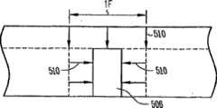
图5A到5C说明常规鳍式场效应晶体管。图5A说明鳍式场效应晶体管的俯视图,且图5B说明鳍式场效应晶体管的沿着线5B-5B的端视图。说明的鳍式场效应晶体管503包含第一源极/漏极区504、第二源极/漏极区505以及在第一与第二源极/漏极区之间延伸的硅鳍506。硅鳍充当晶体管主体,其中第一与第二源极/漏极区之间的沟道是水平的。例如氧化硅的栅极绝缘体507形成于鳍上,且栅极508在氧化物形成于鳍上之后形成于鳍上。说明的常规鳍式场效应晶体管的鳍形成于埋入氧化物509上。图5C说明用于制造鳍式场效应晶体管的鳍的常规蚀刻技术。如图5C说明,鳍宽度通过光刻或电子束光刻和蚀刻来界定。因此,鳍宽度初始为最小特征尺寸(1F)。鳍的宽度随后通过氧化或蚀刻而减小,如箭头510说明。5A-5C illustrate conventional FinFETs. FIG. 5A illustrates a top view of a FinFET, and FIG. 5B illustrates an end view of a FinFET along
发明内容Contents of the invention
本发明标的物的方面使用侧壁间隔物技术来将超薄纳米鳍蚀刻到晶片中,并使用这些经蚀刻的纳米鳍制造具有包围栅极的纳米鳍晶体管。各种实施例在硅衬底中蚀刻硅纳米鳍。将硅纳米鳍用作CMOS晶体管的主体区,其中晶体管主体的厚度与沟道长度均具有小于光刻尺寸的尺寸。举例来说,一些实施例提供具有大约20nm到50nm厚度的超薄纳米鳍。Aspects of the present subject matter use sidewall spacer technology to etch ultra-thin nanofins into wafers and use these etched nanofins to fabricate nanofin transistors with surrounding gates. Various embodiments etch silicon nanofins in a silicon substrate. A silicon nanofin is used as the body region of a CMOS transistor, wherein both the thickness of the transistor body and the channel length have dimensions smaller than the photolithographic dimensions. For example, some embodiments provide ultra-thin nanofins having a thickness of about 20 nm to 50 nm.
本发明标的物的一方面涉及一种用于形成晶体管的方法。根据一实施例,从晶体衬底形成鳍。在所述衬底中在所述鳍下方形成第一源极/漏极区。围绕所述鳍形成包围栅极绝缘体。围绕所述鳍形成包围栅极并通过所述包围栅极绝缘体而与所述鳍分离。在所述鳍的顶部部分中形成第二源极/漏极区。各种实施例在所述衬底上的层中蚀刻孔,在所述孔中形成侧壁间隔物,从所述侧壁间隔物形成鳍图案,以及使用对应于所述鳍图案的掩模来蚀刻进入所述晶体衬底以从所述衬底形成所述鳍。One aspect of the inventive subject matter relates to a method for forming a transistor. According to an embodiment, the fins are formed from a crystalline substrate. A first source/drain region is formed in the substrate below the fin. A surrounding gate insulator is formed around the fin. A surrounding gate is formed around the fin and separated from the fin by the surrounding gate insulator. A second source/drain region is formed in a top portion of the fin. Various embodiments etch holes in layers on the substrate, form sidewall spacers in the holes, form fin patterns from the sidewall spacers, and use masks corresponding to the fin patterns to Etching into the crystalline substrate to form the fins from the substrate.
一方面涉及一种晶体管。一晶体管实施例包含:晶体衬底,其中蚀刻有沟槽以从所述衬底形成晶体半导体鳍;第一源极/漏极区,其在所述晶体衬底中形成于所述鳍的底部,以及第二源极/漏极区,其形成于所述鳍的顶部部分中以在所述第一与第二源极/漏极区之间的所述鳍中界定垂直定向的沟道区。所述晶体管还包含:栅极绝缘体,其围绕所述鳍形成;以及包围栅极,其围绕所述鳍形成且通过所述栅极绝缘体与所述鳍分离。所述鳍具有小于最小特征尺寸的横截面尺寸。One aspect relates to a transistor. A transistor embodiment comprising: a crystalline substrate with trenches etched therein to form crystalline semiconductor fins from the substrate; first source/drain regions formed in the crystalline substrate at the bottom of the fins , and a second source/drain region formed in a top portion of the fin to define a vertically oriented channel region in the fin between the first and second source/drain regions . The transistor also includes a gate insulator formed around the fin, and a surrounding gate formed around the fin and separated from the fin by the gate insulator. The fin has a cross-sectional dimension that is less than a minimum feature dimension.
从以下对本发明标的物的描述和参考图式将明了这些和其它方面、实施例、优点和特征。These and other aspects, embodiments, advantages and features will be apparent from the following description of the subject matter of the invention and from the referenced drawings.
附图说明Description of drawings
图1说明以因数k缩小的多种装置参数的一般趋势和关系。Figure 1 illustrates the general trends and relationships of various device parameters scaled down by a factor k.
图2说明常规硅MOSFET中的亚阈值泄漏。Figure 2 illustrates subthreshold leakage in a conventional silicon MOSFET.
图3说明具有漏极、源极、通过栅极绝缘体与半导体主体分离的前栅极和后栅极的双重栅MOSFET,以及由漏极产生的电场。Figure 3 illustrates a double gate MOSFET with a drain, a source, a front gate and a back gate separated from the semiconductor body by a gate insulator, and the electric field generated by the drain.
图4大体上说明双重栅、双栅和包围栅极MOSFET与常规块状硅MOSFET的亚阈值特性相比的改善的亚阈值特性。Figure 4 generally illustrates the improved subthreshold characteristics of double gate, double gate and surround gate MOSFETs compared to that of conventional bulk silicon MOSFETs.
图5A到5C说明常规鳍式场效应晶体管。5A-5C illustrate conventional FinFETs.
图6A到6L说明根据本发明标的物的各种实施例的用于形成纳米鳍晶体管的过程。6A-6L illustrate processes for forming nanofin transistors according to various embodiments of the present subject matter.
图7说明根据各种实施例的用于纳米鳍晶体管阵列的纳米鳍布局的俯视图。7 illustrates a top view of a nanofin layout for an array of nanofin transistors, according to various embodiments.
图8说明根据本发明标的物的各种实施例的制造纳米鳍晶体管的过程。Figure 8 illustrates the process of fabricating a nanofin transistor according to various embodiments of the present subject matter.
图9说明根据本发明标的物的各种实施例的从晶体衬底形成鳍的过程。Figure 9 illustrates the process of forming fins from a crystalline substrate according to various embodiments of the present subject matter.
图10是根据本发明标的物的各种实施例的存储器装置的各种实施例的高级组织的简化框图。Figure 10 is a simplified block diagram of the high-level organization of various embodiments of a memory device in accordance with various embodiments of the present subject matter.
图11说明根据各种实施例的具有一个或一个以上纳米鳍晶体管的电子系统的图。11 illustrates a diagram of an electronic system with one or more nanofin transistors, according to various embodiments.
图12描绘具有控制器和存储器的系统的实施例的图。Figure 12 depicts a diagram of an embodiment of a system with a controller and memory.
具体实施方式Detailed ways
以下具体实施方式涉及附图,附图以说明的方式展示可实践本发明标的物的特定方面和实施例。充分详细描述这些实施例以使所属领域的技术人员能够实践本发明标的物。本发明标的物的各种实施例不一定相互排斥,因为一个实施例的方面可与另一实施例的方面组合。在不脱离本发明标的物的范围的情况下可利用其它实施例且可做出结构、逻辑和电气改变。在以下描述中,术语“晶片”和“衬底”可互换使用以大体上指代上面形成集成电路的任何结构,且还指代在集成电路制造的各个阶段期间的此类结构。两个术语均包含掺杂和未掺杂半导体、支撑半导体或绝缘材料上的半导体的外延层、此类层的组合以及此项技术中已知的其它此类结构。本申请案中使用的术语“水平”界定为平行于晶片或衬底的常规平面或表面的平面,无论晶片或衬底的定向如何。术语“垂直”指代垂直于上文界定的水平的方向。例如“在...上”、“侧面”、“较高”、“较低”、“上方”和“下方”的前置词是相对于在晶片或衬底的顶面上的常规平面或表面而界定的,无论晶片或衬底的定向如何。因此,以下具体实施方式不应以限制性意义来理解,且本发明的范围仅由所附权利要求书以及此权利要求书具有的等效物的完整范围来界定。The following detailed description refers to the accompanying drawings, which show, by way of illustration, certain aspects and embodiments in which the subject matter of the invention may be practiced. These embodiments are described in sufficient detail to enable those skilled in the art to practice the inventive subject matter. The various embodiments of the present subject matter are not necessarily mutually exclusive, as aspects of one embodiment may be combined with aspects of another embodiment. Other embodiments may be utilized and structural, logical, and electrical changes may be made without departing from the scope of the present subject matter. In the following description, the terms "wafer" and "substrate" are used interchangeably to refer generally to any structure on which integrated circuits are formed, and also to refer to such structures during various stages of integrated circuit fabrication. Both terms encompass doped and undoped semiconductors, epitaxial layers of semiconductors on supporting or insulating materials, combinations of such layers, and other such structures known in the art. The term "horizontal" as used in this application is defined as a plane parallel to the general plane or surface of a wafer or substrate, regardless of the orientation of the wafer or substrate. The term "vertical" refers to a direction perpendicular to the horizontal defined above. Prepositions such as "on," "side," "upper," "lower," "above," and "below" are relative to a generally planar or surface, regardless of the orientation of the wafer or substrate. Accordingly, the following detailed description should not be taken in a limiting sense, and the scope of the invention is defined only by the appended claims, along with the full scope of equivalents to which such claims are entitled.
本文揭示纳米鳍晶体管以及将纳米鳍蚀刻到衬底或晶片中并用于制作单晶体纳米鳍晶体管的制造技术。以下论述涉及硅纳米鳍实施例。在阅读和理解本发明之后,所属领域的技术人员将了解如何使用其它半导体来形成纳米鳍。本发明标的物的方面提供具有垂直沟道的纳米鳍晶体管,其中在鳍的底部存在第一源极/漏极区,在鳍的顶部存在第二源极/漏极区。图6A到6L说明根据本发明标的物的各种实施例形成纳米鳍晶体管的过程。Nanofin transistors and fabrication techniques for etching nanofins into substrates or wafers and for making single crystal nanofin transistors are disclosed herein. The following discussion refers to silicon nanofin embodiments. After reading and understanding this disclosure, those skilled in the art will understand how to use other semiconductors to form nanofins. Aspects of the present subject matter provide a nanofin transistor having a vertical channel in which there is a first source/drain region at the bottom of the fin and a second source/drain region at the top of the fin. 6A-6L illustrate the process of forming nanofin transistors according to various embodiments of the present subject matter.
将氮化硅沉积在硅晶片上,且用非晶硅(a-硅)层覆盖氮化硅。图6A说明在非晶硅613中界定孔612且形成侧壁间隔物614之后的结构611的侧视图。孔612延伸到氮化硅层615,该层置于例如硅晶片的衬底616上。各种实施例通过氧化非晶硅来形成侧壁间隔物。图6B说明在用厚非晶硅层616覆盖结构之后结构611的侧视图。图6C说明在将结构平面化(如箭头说明)至少达到移除非晶硅顶部上的氧化物的程度之后的结构611。可使用例如化学机械抛光(CMP)工艺来平面化所述结构。这留下暴露于表面上的氧化物614的伸长矩形图案,也称为“跑道”(racetrack)图案。图案线的宽度由氧化物厚度而不是遮蔽和光刻来确定。举例来说,根据各种实施例,氧化物厚度可在大约20nm到50nm的范围内。Silicon nitride is deposited on the silicon wafer and covered with a layer of amorphous silicon (a-silicon). 6A illustrates a side view of
图6D说明跑道图案上的掩模,其选择性覆盖氧化物的部分并暴露氧化物的其它部分。由阴影条说明的暴露的氧化物部分被移除。执行例如氢氧化钾(KOH)蚀刻的蚀刻工艺以移除非晶硅。氧化物或在图6D说明的掩蔽和蚀刻之后保留的氧化物的部分在蚀刻期间保护氮化物。在移除非晶硅之后可蚀刻氮化物615,随后进行方向性硅蚀刻,其将晶片616蚀刻到氮化物层下方的预定深度。氮化物图案保护局部硅区域免于蚀刻,导致硅的硅鳍617从硅晶片的现在较低的表面突出,如图6E说明。图6F和6G说明在鳍的顶部和鳍的底部处的沟槽用掺杂剂植入之后的结构的俯视图和侧视图。如图6F说明,沟槽中的掺杂剂形成导电线618(例如,源极线)。掺杂剂还在鳍的底部或底部部分处形成源极/漏极区。因为鳍极薄,所以沟槽中的掺杂能够在鳍下方完全扩散。条可在行或列方向上。Figure 6D illustrates a mask over a racetrack pattern that selectively covers portions of the oxide and exposes other portions of the oxide. The exposed oxide portions illustrated by the shaded bars were removed. An etching process such as potassium hydroxide (KOH) etching is performed to remove the amorphous silicon. The oxide, or the portion of the oxide that remains after masking and etching illustrated in Figure 6D, protects the nitride during etching. The
图6H说明在围绕鳍617形成栅极绝缘体619且围绕栅极绝缘体形成并通过栅极绝缘体与鳍分离栅极材料620之后的结构611。举例来说,一实施例使用热氧化工艺来氧化硅鳍。根据各个实施例,栅极材料620可以是多晶硅或金属。6H illustrates
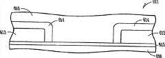
图6I和6J分别说明第一阵列实施例的俯视图和沿着线6J-6J的横截面图。结构611用绝缘体621(例如,氧化物)回填,且在鳍的侧面上产生沟槽。可沉积并方向性蚀刻例如多晶硅或金属的栅极布线材料622以仅保留在侧壁上并接触用于鳍的包围栅极620。可蚀刻栅极材料和栅极布线材料以使其凹入鳍的顶部下方。整个结构可再次用氧化物回填并平面化以在表面上仅留下氧化物。接着可蚀刻接触开口和漏极掺杂区到达柱和经植入的漏极区的顶部,且通过常规技术制成与漏极区的金属接触件。在此情况下,金属布线可在“x方向”上行进,且埋入的源极布线可垂直于图解中的纸张平面而行进。6I and 6J illustrate a top view and a cross-sectional view along line 6J-6J, respectively, of a first array embodiment.
图6K和6L分别说明第二阵列实施例的俯视图和沿着线6L-6L的横截面图。结构611用绝缘体621(例如,氧化物)回填,且在“y方向”上于鳍617的侧面上产生沟槽。可沉积并方向性蚀刻例如多晶硅或金属的栅极布线材料622以仅保留在侧壁上并接触鳍上的栅极。可蚀刻栅极材料和栅极布线材料以使其凹入鳍的顶部下方。整个结构可用绝缘体(例如,氧化物)回填并平面化以在表面上仅留下氧化物。接着可蚀刻接触开口和漏极掺杂区到达柱和经植入的漏极区的顶部,且通过常规技术制成与漏极区的金属接触件。在此情况下,金属布线可垂直于图解中的纸张平面而行进,且埋入的源极布线可在“x方向”上行进。6K and 6L illustrate a top view and a cross-sectional view along line 6L-6L, respectively, of a second array embodiment.
在第一和第二阵列实施例中,埋入的源极/漏极可在形成包围栅极绝缘体和包围栅极之前植入。图6L说明具有漏极/源极区623和624、凹入栅极620以及源极/漏极区布线618的完成鳍结构中的一者。这些纳米鳍场效应晶体管可具有大的W/L比率且将比纳米线场效应晶体管传导更多电流。In the first and second array embodiments, the buried source/drain can be implanted before forming the surrounding gate insulator and surrounding gate. FIG. 6L illustrates one of the completed fin structures with drain/
图7说明根据各种实施例的用于纳米鳍晶体管阵列的纳米鳍布局的俯视图。图说明侧壁间隔物714的两个“跑道”,且进一步说明通过蚀刻移除的侧壁间隔物的部分。用于形成侧壁间隔物轨道的孔以最小特征尺寸(1F)形成。掩模条725具有最小特征尺寸(1F)的宽度,且以最小特征尺寸(1F)分离。在说明的布局中,纳米鳍的列具有大约2F的中心到中心间距,且纳米鳍的行具有大约1F的中心到中心间距。而且,如图7说明,由于纳米鳍由孔的壁上的侧壁间隔物形成,因此第一与第二行之间的中心到中心间距将比1F尺寸略小出对应于纳米鳍厚度的量(1F-△T),且第二与第三行之间的中心到中心间距将比1F略大出对应于纳米鳍厚度的量(1F+△T)。大体上,第一与第二行之间的中心到中心间距将比特征尺寸间隔(NF)略小出对应于纳米鳍厚度的量(NF-△T),且第二与第三行之间的中心到中心间距将比特征尺寸间隔(NF)略大出对应于纳米鳍厚度的量(NF+△T)。7 illustrates a top view of a nanofin layout for an array of nanofin transistors, according to various embodiments. The figure illustrates the two "race tracks" of the
图8说明根据本发明标的物的各种实施例的制造纳米鳍晶体管的过程。在826,从晶体衬底形成鳍。举例来说,可从例如硅晶片的晶片蚀刻鳍。在827,在衬底中在鳍的底部形成第一源极/漏极区。因为鳍较薄,所以掺杂剂能够在鳍的整个占据面积下方扩散。在828,围绕鳍形成包围栅极绝缘体,且在829,围绕鳍形成包围栅极并通过包围栅极绝缘体而与鳍分离。在830用绝缘体回填所得结构。蚀刻沟槽且邻近于并接触包围栅极而形成栅极线,如831说明。一些实施例形成与包围栅极的相对侧面接触的两个栅极线。栅极线可经定向以在纳米鳍结构的长侧上接触包围栅极,或可经定向以在纳米鳍结构的短侧上接触包围栅极。也就是说,栅极线可在列或行方向上形成。在832,在鳍的顶部部分中形成第二源极/漏极区,且在833形成用于第二源极/漏极区的接触件。Figure 8 illustrates the process of fabricating a nanofin transistor according to various embodiments of the present subject matter. At 826, fins are formed from the crystalline substrate. For example, fins may be etched from a wafer such as a silicon wafer. At 827, a first source/drain region is formed in the substrate at the bottom of the fin. Because the fin is thin, dopants are able to diffuse under the entire footprint of the fin. At 828 a surrounding gate insulator is formed around the fin, and at 829 a surrounding gate is formed around the fin and separated from the fin by the surrounding gate insulator. The resulting structure is backfilled at 830 with insulator. A gate line is formed by etching the trench adjacent to and contacting the surrounding gate, as illustrated at 831 . Some embodiments form two gate lines in contact with opposite sides surrounding the gate. The gate line may be oriented to contact the surrounding gate on the long side of the nanofin structure, or may be oriented to contact the surrounding gate on the short side of the nanofin structure. That is, gate lines may be formed in a column or row direction. At 832 , a second source/drain region is formed in the top portion of the fin, and at 833 a contact for the second source/drain region is formed.
图9说明根据本发明标的物的各种实施例的例如在图8中的826说明从晶体衬底形成鳍的过程。在934在晶体衬底上形成一层,且在935在所述层中蚀刻或另外形成孔。在各种实施例中,形成于晶体衬底上的层是非晶硅层,其中氮化硅层夹在晶体衬底与非晶硅之间,且蚀刻孔到达氮化硅层。在936,在孔中抵靠界定孔外围的层的壁形成侧壁间隔物。各种实施例使非晶硅层氧化以形成侧壁间隔物。在937用第一层的材料(例如,a-硅)回填孔,且将结构平面化。在图6B和6C说明的实施例中,平面化移除非晶硅顶面上的氧化物,留下氧化物侧壁间隔物的“跑道”或矩形图案。在938,从侧壁间隔物形成鳍图案,例如,比如可使用遮蔽和蚀刻工艺来实现。在一些实施例中,所得鳍图案具有在第一方向上的对应于最小特征尺寸的第一横截面厚度,以及在正交于第一方向的第二方向上的对应于氧化物侧壁厚度且显著小于最小特征尺寸的第二横截面厚度。在939,移除所述层(例如,a-硅),留下侧壁间隔物的鳍图案。在940使用对应于侧壁间隔物的鳍图案的掩模来蚀刻晶体衬底。各种实施例将氮化硅层蚀刻到鳍图案中,且接着在蚀刻衬底时使用氮化硅层来遮蔽具有鳍图案的晶体衬底。在941,移除掩模层(例如,氮化硅)以暴露经蚀刻的鳍的顶部。Figure 9 illustrates a process of forming fins from a crystalline substrate, such as illustrated at 826 in Figure 8, in accordance with various embodiments of the inventive subject matter. A layer is formed on the crystalline substrate at 934 and holes are etched or otherwise formed in the layer at 935 . In various embodiments, the layer formed on the crystalline substrate is an amorphous silicon layer, wherein a silicon nitride layer is sandwiched between the crystalline substrate and the amorphous silicon, and holes are etched to the silicon nitride layer. At 936, sidewall spacers are formed in the hole against the walls of the layer defining the periphery of the hole. Various embodiments oxidize the amorphous silicon layer to form sidewall spacers. The holes are backfilled at 937 with the material of the first layer (eg, a-silicon) and the structure is planarized. In the embodiment illustrated in Figures 6B and 6C, planarization removes the oxide on the top surface of the amorphous silicon, leaving a "race track" or rectangular pattern of oxide sidewall spacers. At 938, a fin pattern is formed from the sidewall spacers, such as may be accomplished using a masking and etching process, for example. In some embodiments, the resulting fin pattern has a first cross-sectional thickness in a first direction corresponding to a minimum feature size, and a thickness corresponding to an oxide sidewall in a second direction orthogonal to the first direction and The second cross-sectional thickness is substantially less than the smallest feature dimension. At 939, the layer (eg, a-silicon) is removed, leaving a fin pattern of sidewall spacers. The crystalline substrate is etched at 940 using a mask corresponding to the fin pattern of the sidewall spacers. Various embodiments etch a silicon nitride layer into the fin pattern, and then use the silicon nitride layer to mask the crystalline substrate with the fin pattern when etching the substrate. At 941, the masking layer (eg, silicon nitride) is removed to expose the tops of the etched fins.
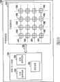
图10是根据本发明标的物的各种实施例的存储器装置的各种实施例的高级组织的简化框图。说明的存储器装置1042包含存储器阵列1043以及读取/写入控制电路1044以经由通信线或通道1045对存储器阵列执行操作。说明的存储器装置1042可以是存储卡或存储器模块,例如单列直插存储器模块(SIMM)和双列直插存储器模块(DIMM)。在阅读和理解本发明之后,所属领域的技术人员将了解,存储器阵列和/或控制电路中的半导体组件能够使用经蚀刻的纳米鳍晶体管来制造,如上文所述。上文已描述用于这些装置的结构和制造方法。Figure 10 is a simplified block diagram of the high-level organization of various embodiments of a memory device in accordance with various embodiments of the present subject matter. The illustrated
存储器阵列1043包含若干存储器单元1046。阵列中的存储器单元排列成行和列。在各种实施例中,字线1047连接行中的存储器单元,且位线1048连接列中的存储器单元。读取/写入控制电路1044包含用以选择所需行的字线选择电路1049,用以选择所需列的位线选择电路1050以及用以针对存储器阵列1043中的选定存储器单元检测存储器状态的读取电路1051。
图11说明根据各种实施例的具有一个或一个以上纳米鳍晶体管的电子系统1152的图。电子系统1152包含控制器1153、总线1154以及电子装置1155,其中总线1154提供控制器1153与电子装置1155之间的通信通道。在各种实施例中,控制器和/或电子装置包含如本文先前论述的纳米鳍晶体管。说明的电子系统1152可包含但不限于信息处理装置、无线系统、电信系统、光纤系统、电光系统以及计算机。11 illustrates a diagram of an
图12描绘具有控制器1257和存储器1258的系统1256的实施例的图。控制器和/或存储器可包含根据各种实施例的纳米鳍晶体管。说明的系统1256还包含电子设备1259和总线1260,总线1260用于提供控制器与电子设备之间以及控制器与存储器之间的通信通道。总线可包含每一者独立配置的地址、数据总线和控制总线,或可使用共同的通信通道来提供地址、数据和/或控制,其使用由控制器调节。在一实施例中,电子设备1259可以是类似于存储器1258配置的额外存储器。一实施例可包含耦合到总线1260的一个或多个外围装置1261。外围装置可包含显示器、额外存储器或可结合控制器和/或存储器操作的其它控制装置。在一实施例中,控制器是处理器。控制器1257、存储器1258、电子设备1259以及外围装置1261中的任一者可包含根据各种实施例的纳米鳍晶体管。系统1256可包含但不限于信息处理装置、电信系统和计算机。含有本发明中描述的纳米鳍晶体管的应用包含用于存储器模块、装置驱动器、功率模块、通信调制解调器、处理器模块以及专用模块中的电子系统,且可包含多层多芯片模块。此电路可进一步为例如时钟、电视机、手机、个人计算机、汽车、工业控制系统、飞机等多种电子系统的子组件。FIG. 12 depicts a diagram of an embodiment of a system 1256 having a controller 1257 and memory 1258 . A controller and/or memory may include nanofin transistors according to various embodiments. The illustrated system 1256 also includes electronics 1259 and a bus 1260 for providing communication channels between the controller and the electronics, and between the controller and the memory. The bus may include address, data and control buses each configured independently, or a common communication channel may be used to provide address, data and/or control, the use of which is regulated by the controller. In an embodiment, electronic device 1259 may be an additional memory configured similarly to memory 1258 . An embodiment may include one or more peripheral devices 1261 coupled to bus 1260 . Peripheral devices may include a display, additional memory, or other control devices operable in conjunction with a controller and/or memory. In one embodiment, the controller is a processor. Any of the controller 1257, memory 1258, electronics 1259, and peripherals 1261 may include nanofin transistors according to various embodiments. System 1256 may include, but is not limited to, information processing devices, telecommunications systems, and computers. Applications incorporating the nanofin transistors described in this disclosure include electronic systems used in memory modules, device drivers, power modules, communication modems, processor modules, and application-specific modules, and may include multilayer multi-chip modules. This circuit can further be a sub-assembly of various electronic systems such as clocks, televisions, mobile phones, personal computers, automobiles, industrial control systems, airplanes, etc.
存储器可实现为含有根据各种实施例的纳米鳍晶体管的存储器装置。应了解,实施例同等适用于任何尺寸和类型的存储器电路,且不希望限于特定类型的存储器装置。存储器类型包含DRAM、SRAM(静态随机存取存储器)或快闪存储器。另外,DRAM可以是同步DRAM,通常称为SGRAM(同步图形随机存取存储器)、SDRAM(同步动态随机存取存储器)、SDRAM II以及DDR SDRAM(双数据速率SDRAM)。各种出现的存储器技术能够使用具有压缩应变沟道的晶体管。A memory may be implemented as a memory device containing nanofin transistors according to various embodiments. It should be appreciated that the embodiments are equally applicable to any size and type of memory circuit, and are not intended to be limited to a particular type of memory device. Memory types include DRAM, SRAM (Static Random Access Memory) or flash memory. Additionally, the DRAM may be synchronous DRAM, commonly referred to as SGRAM (Synchronous Graphical Random Access Memory), SDRAM (Synchronous Dynamic Random Access Memory), SDRAM II, and DDR SDRAM (Double Data Rate SDRAM). Various emerging memory technologies are able to use transistors with compressively strained channels.
本发明包含若干过程、电路图和单元结构。本发明标的物不限于特定过程顺序或逻辑布置。尽管本文已说明和描述了特定实施例,但所属领域的技术人员将了解,经计划以实现相同目的的任何布置均可代替所示的特定实施例。本申请案希望涵盖对本发明标的物的改动或变化。应了解,希望上文描述是说明性的而不是限制性的。所属领域的技术人员在审阅和理解上文描述之后将了解上述实施例和其它实施例的组合。应参考所附权利要求书以及此权利要求书具有的等效物的完整范围来确定本发明标的物的范围。The invention includes several processes, circuit diagrams and unit structures. The inventive subject matter is not limited to a specific process order or logical arrangement. Although specific embodiments have been illustrated and described herein, those skilled in the art will appreciate that any arrangement that is designed to achieve the same purpose may be substituted for the specific embodiments shown. This application is intended to cover adaptations or variations of the present subject matter. It should be understood that the foregoing description is intended to be illustrative rather than restrictive. Combinations of the above-described embodiments and other embodiments will be apparent to those of ordinary skill in the art upon review and understanding of the above description. The scope of the inventive subject matter should be determined with reference to the appended claims, along with the full range of equivalents to which such claims are entitled.
Claims (35)
Translated fromChineseApplications Claiming Priority (11)
| Application Number | Priority Date | Filing Date | Title |
|---|---|---|---|
| US11/397,358 | 2006-04-04 | ||
| US11/397,527 | 2006-04-04 | ||
| US11/397,430US8734583B2 (en) | 2006-04-04 | 2006-04-04 | Grown nanofin transistors |
| US11/397,413 | 2006-04-04 | ||
| US11/397,527US7425491B2 (en) | 2006-04-04 | 2006-04-04 | Nanowire transistor with surrounding gate |
| US11/397,413US7491995B2 (en) | 2006-04-04 | 2006-04-04 | DRAM with nanofin transistors |
| US11/397,406US20070228491A1 (en) | 2006-04-04 | 2006-04-04 | Tunneling transistor with sublithographic channel |
| US11/397,358US8354311B2 (en) | 2006-04-04 | 2006-04-04 | Method for forming nanofin transistors |
| US11/397,430 | 2006-04-04 | ||
| US11/397,406 | 2006-04-04 | ||
| PCT/US2007/008400WO2007114927A1 (en) | 2006-04-04 | 2007-04-03 | Etched nanofin transistors |
Publications (2)
| Publication Number | Publication Date |
|---|---|
| CN101416317A CN101416317A (en) | 2009-04-22 |
| CN101416317Btrue CN101416317B (en) | 2013-03-13 |
Family
ID=38559686
Family Applications (4)
| Application Number | Title | Priority Date | Filing Date |
|---|---|---|---|
| CN2007800121748AActiveCN101416317B (en) | 2006-04-04 | 2007-04-03 | Etched nanofin transistors |
| CN2007800110847AActiveCN101410961B (en) | 2006-04-04 | 2007-04-03 | Grown nanofin transistors |
| CNA2007800120849APendingCN101416288A (en) | 2006-04-04 | 2007-04-03 | Grown nanofin transistors |
| CN2007800111642AActiveCN101410963B (en) | 2006-04-04 | 2007-04-03 | Nanowire transistor with surrounding gate and method of manufacturing the same |
Family Applications After (3)
| Application Number | Title | Priority Date | Filing Date |
|---|---|---|---|
| CN2007800110847AActiveCN101410961B (en) | 2006-04-04 | 2007-04-03 | Grown nanofin transistors |
| CNA2007800120849APendingCN101416288A (en) | 2006-04-04 | 2007-04-03 | Grown nanofin transistors |
| CN2007800111642AActiveCN101410963B (en) | 2006-04-04 | 2007-04-03 | Nanowire transistor with surrounding gate and method of manufacturing the same |
Country Status (3)
| Country | Link |
|---|---|
| US (4) | US7425491B2 (en) |
| CN (4) | CN101416317B (en) |
| TW (1) | TWI344181B (en) |
Families Citing this family (72)
| Publication number | Priority date | Publication date | Assignee | Title |
|---|---|---|---|---|
| US8464299B1 (en) | 2004-11-17 | 2013-06-11 | Rockstar Consortium Us Lp | Resource conservation for packet television services |
| US7326611B2 (en)* | 2005-02-03 | 2008-02-05 | Micron Technology, Inc. | DRAM arrays, vertical transistor structures and methods of forming transistor structures and DRAM arrays |
| US7768051B2 (en) | 2005-07-25 | 2010-08-03 | Micron Technology, Inc. | DRAM including a vertical surround gate transistor |
| US7485908B2 (en)* | 2005-08-18 | 2009-02-03 | United States Of America As Represented By The Secretary Of The Air Force | Insulated gate silicon nanowire transistor and method of manufacture |
| KR100790863B1 (en)* | 2005-12-28 | 2008-01-03 | 삼성전자주식회사 | Nano wire manufacturing method |
| US20070228491A1 (en)* | 2006-04-04 | 2007-10-04 | Micron Technology, Inc. | Tunneling transistor with sublithographic channel |
| US7491995B2 (en) | 2006-04-04 | 2009-02-17 | Micron Technology, Inc. | DRAM with nanofin transistors |
| US8734583B2 (en)* | 2006-04-04 | 2014-05-27 | Micron Technology, Inc. | Grown nanofin transistors |
| US8354311B2 (en)* | 2006-04-04 | 2013-01-15 | Micron Technology, Inc. | Method for forming nanofin transistors |
| US7425491B2 (en) | 2006-04-04 | 2008-09-16 | Micron Technology, Inc. | Nanowire transistor with surrounding gate |
| US7667260B2 (en)* | 2006-08-09 | 2010-02-23 | Micron Technology, Inc. | Nanoscale floating gate and methods of formation |
| US7999251B2 (en) | 2006-09-11 | 2011-08-16 | International Business Machines Corporation | Nanowire MOSFET with doped epitaxial contacts for source and drain |
| EP1900681B1 (en)* | 2006-09-15 | 2017-03-15 | Imec | Tunnel Field-Effect Transistors based on silicon nanowires |
| US7893476B2 (en)* | 2006-09-15 | 2011-02-22 | Imec | Tunnel effect transistors based on silicon nanowires |
| KR100866966B1 (en)* | 2007-05-10 | 2008-11-06 | 삼성전자주식회사 | Nonvolatile Memory Devices, Manufacturing Methods And Semiconductor Packages |
| US9449831B2 (en) | 2007-05-25 | 2016-09-20 | Cypress Semiconductor Corporation | Oxide-nitride-oxide stack having multiple oxynitride layers |
| US20090179253A1 (en) | 2007-05-25 | 2009-07-16 | Cypress Semiconductor Corporation | Oxide-nitride-oxide stack having multiple oxynitride layers |
| US8940645B2 (en) | 2007-05-25 | 2015-01-27 | Cypress Semiconductor Corporation | Radical oxidation process for fabricating a nonvolatile charge trap memory device |
| US8633537B2 (en) | 2007-05-25 | 2014-01-21 | Cypress Semiconductor Corporation | Memory transistor with multiple charge storing layers and a high work function gate electrode |
| US7892956B2 (en)* | 2007-09-24 | 2011-02-22 | International Business Machines Corporation | Methods of manufacture of vertical nanowire FET devices |
| US7897494B2 (en)* | 2008-06-24 | 2011-03-01 | Imec | Formation of single crystal semiconductor nanowires |
| DE102008030853B4 (en)* | 2008-06-30 | 2014-04-30 | Globalfoundries Dresden Module One Limited Liability Company & Co. Kg | Three-dimensional transistor with a dual-channel configuration |
| KR101417764B1 (en)* | 2008-09-26 | 2014-07-09 | 삼성전자주식회사 | Vertical semiconductor device and manufacturing method thereof |
| US7816275B1 (en)* | 2009-04-03 | 2010-10-19 | International Business Machines Corporation | Gate patterning of nano-channel devices |
| EP2472585B1 (en)* | 2009-09-30 | 2022-07-06 | National University Corporation Hokkaido University | Tunnel field effect transistor and method for manufacturing same |
| US8368127B2 (en)* | 2009-10-08 | 2013-02-05 | Globalfoundries Singapore Pte., Ltd. | Method of fabricating a silicon tunneling field effect transistor (TFET) with high drive current |
| EP2315239A1 (en)* | 2009-10-23 | 2011-04-27 | Imec | A method of forming monocrystalline germanium or silicon germanium |
| US20110127492A1 (en)* | 2009-11-30 | 2011-06-02 | International Business Machines Corporation | Field Effect Transistor Having Nanostructure Channel |
| US8841652B2 (en)* | 2009-11-30 | 2014-09-23 | International Business Machines Corporation | Self aligned carbide source/drain FET |
| US8466034B2 (en)* | 2010-03-29 | 2013-06-18 | GlobalFoundries, Inc. | Method of manufacturing a finned semiconductor device structure |
| CN101969061A (en)* | 2010-09-27 | 2011-02-09 | 复旦大学 | Fin-type tunneling transistor integrated circuit and manufacturing method thereof |
| CN102201343A (en)* | 2011-04-26 | 2011-09-28 | 复旦大学 | Preparation method of Nano MOS (Metal Oxide Semiconductor) device and Nano MOS device |
| CN102184961B (en)* | 2011-04-26 | 2017-04-12 | 复旦大学 | Asymmetrical gate metal oxide semiconductor (MOS) device and manufacturing method thereof |
| US8728892B2 (en)* | 2011-05-05 | 2014-05-20 | Taiwan Semiconductor Manufacturing Company, Ltd. | Adaptive fin design for FinFETs |
| CN102214595B (en)* | 2011-05-26 | 2012-10-10 | 北京大学 | Fabrication method of gate-enclosed silicon nanowire transistor with air as sidewall |
| CN102254948B (en)* | 2011-07-29 | 2012-10-10 | 北京大学 | Tunneling field effect transistor with double surrounding gate structure and preparation method thereof |
| JP2013088862A (en)* | 2011-10-13 | 2013-05-13 | Elpida Memory Inc | Layout data creation device and semiconductor device |
| CN102569405B (en)* | 2012-01-17 | 2014-02-19 | 清华大学 | Tunneling transistor with quasi-coaxial cable structure and method of forming same |
| CN102544105B (en)* | 2012-01-17 | 2015-04-15 | 清华大学 | Tunnel transistor with quasi-coaxial cable structure and forming method thereof |
| KR101908355B1 (en) | 2012-03-20 | 2018-10-16 | 삼성전자주식회사 | Semiconductor Device and Method of manufacturing the same |
| US9064745B2 (en) | 2012-08-29 | 2015-06-23 | International Business Machines Corporation | Sublithographic width finFET employing solid phase epitaxy |
| US8796085B2 (en) | 2012-10-12 | 2014-08-05 | Viktor Koldiaev | Vertical super-thin body semiconductor on dielectric wall devices and methods of their fabrication |
| KR102050561B1 (en)* | 2012-12-18 | 2020-01-09 | 삼성디스플레이 주식회사 | Vertical thin film transistor and fabrivating method thereof |
| CN103137563A (en)* | 2013-02-20 | 2013-06-05 | 上海华力微电子有限公司 | Flash memory structure achieved on vertical silicon nanometer line and manufacturing method of flash memory structure |
| US8975123B2 (en) | 2013-07-09 | 2015-03-10 | International Business Machines Corporation | Tunnel field-effect transistors with a gate-swing broken-gap heterostructure |
| US9306063B2 (en) | 2013-09-27 | 2016-04-05 | Intel Corporation | Vertical transistor devices for embedded memory and logic technologies |
| CN104900696B (en)* | 2014-03-04 | 2019-02-15 | 中芯国际集成电路制造(上海)有限公司 | Vertical nanowire MOS transistor and method of forming the same |
| US9673209B2 (en)* | 2014-05-16 | 2017-06-06 | Taiwan Semiconductor Manufacturing Company, Ltd. | Memory device and method for fabricating the same |
| US10361090B2 (en) | 2014-06-13 | 2019-07-23 | Intel Corporation | Vertical channel transistors fabrication process by selective subtraction of a regular grid |
| US10418271B2 (en)* | 2014-06-13 | 2019-09-17 | Taiwan Semiconductor Manufacturing Co., Ltd. | Method of forming isolation layer |
| CN105470258B (en)* | 2014-06-18 | 2020-04-24 | 上海华力微电子有限公司 | SONOS B4-flash memory |
| US9711596B2 (en)* | 2014-06-24 | 2017-07-18 | Taiwan Semiconductor Manufacturing Company Limited | Semiconductor device including a semiconductor sheet interconnecting a source region and a drain region |
| JP6428789B2 (en)* | 2014-06-24 | 2018-11-28 | インテル・コーポレーション | Integrated circuits, complementary metal oxide semiconductor (CMOS) devices, computing systems, and methods |
| US9786774B2 (en)* | 2014-06-27 | 2017-10-10 | Taiwan Semiconductor Manufacturing Company, Ltd. | Metal gate of gate-all-around transistor |
| US9570612B2 (en)* | 2014-06-27 | 2017-02-14 | Taiwan Semiconductor Manufacturing Company Limited | Method and structure for straining carrier channel in vertical gate all-around device |
| US9698261B2 (en)* | 2014-06-30 | 2017-07-04 | Taiwan Semiconductor Manufacturing Co., Ltd. | Vertical device architecture |
| US9318447B2 (en) | 2014-07-18 | 2016-04-19 | Taiwan Semiconductor Manufacturing Company Limited | Semiconductor device and method of forming vertical structure |
| US9716161B2 (en)* | 2014-10-01 | 2017-07-25 | Taiwan Semiconductor Manufacturing Co., Ltd. | Gate structure having designed profile and method for forming the same |
| US9508858B2 (en) | 2014-11-18 | 2016-11-29 | Taiwan Semiconductor Manufacturing Company, Ltd. | Contacts for highly scaled transistors |
| US9472468B2 (en)* | 2014-12-11 | 2016-10-18 | Taiwan Semiconductor Manufacturing Company, Ltd. | Nanowire CMOS structure and formation methods |
| CN104617137B (en)* | 2015-01-19 | 2018-09-21 | 华为技术有限公司 | A kind of fieldtron and preparation method thereof |
| CN106033725B (en)* | 2015-03-13 | 2020-10-16 | 联华电子股份有限公司 | Semiconductor element and manufacturing process thereof |
| US9520466B2 (en)* | 2015-03-16 | 2016-12-13 | Taiwan Semiconductor Manufacturing Company, Ltd. | Vertical gate-all-around field effect transistors and methods of forming same |
| US9799776B2 (en)* | 2015-06-15 | 2017-10-24 | Stmicroelectronics, Inc. | Semi-floating gate FET |
| US9825093B2 (en)* | 2015-08-21 | 2017-11-21 | Globalfoundries Inc. | FinFET PCM access transistor having gate-wrapped source and drain regions |
| US9818873B2 (en)* | 2015-10-09 | 2017-11-14 | Globalfoundries Inc. | Forming stressed epitaxial layers between gates separated by different pitches |
| KR102651871B1 (en) | 2016-11-29 | 2024-04-01 | 삼성전자주식회사 | Semiconductor device and method for manufacturing the same |
| US10592698B2 (en) | 2017-03-01 | 2020-03-17 | International Business Machines Corporation | Analog-based multiple-bit chip security |
| US10186510B2 (en)* | 2017-05-01 | 2019-01-22 | Advanced Micro Devices, Inc. | Vertical gate all around library architecture |
| CN108493112A (en)* | 2018-03-12 | 2018-09-04 | 浙江大学 | A kind of manufacturing method of laminated type polysilicon fet device |
| KR20220034051A (en)* | 2019-07-11 | 2022-03-17 | 유니산티스 일렉트로닉스 싱가포르 프라이빗 리미티드 | Columnar semiconductor device and its manufacturing method |
| CN115188762A (en)* | 2022-07-13 | 2022-10-14 | 长鑫存储技术有限公司 | Semiconductor memory device and method of forming the same |
Family Cites Families (64)
| Publication number | Priority date | Publication date | Assignee | Title |
|---|---|---|---|---|
| US4941026A (en) | 1986-12-05 | 1990-07-10 | General Electric Company | Semiconductor devices exhibiting minimum on-resistance |
| US5013680A (en) | 1990-07-18 | 1991-05-07 | Micron Technology, Inc. | Process for fabricating a DRAM array having feature widths that transcend the resolution limit of available photolithography |
| JP3219307B2 (en) | 1991-08-28 | 2001-10-15 | シャープ株式会社 | Semiconductor device structure and manufacturing method |
| JP3549602B2 (en) | 1995-01-12 | 2004-08-04 | 株式会社ルネサステクノロジ | Semiconductor storage device |
| JP3732884B2 (en)* | 1996-04-22 | 2006-01-11 | 株式会社ルネサステクノロジ | Internal power supply voltage generation circuit, internal voltage generation circuit, and semiconductor device |
| US5874760A (en)* | 1997-01-22 | 1999-02-23 | International Business Machines Corporation | 4F-square memory cell having vertical floating-gate transistors with self-aligned shallow trench isolation |
| US5990509A (en)* | 1997-01-22 | 1999-11-23 | International Business Machines Corporation | 2F-square memory cell for gigabit memory applications |
| US5973356A (en)* | 1997-07-08 | 1999-10-26 | Micron Technology, Inc. | Ultra high density flash memory |
| US6150687A (en) | 1997-07-08 | 2000-11-21 | Micron Technology, Inc. | Memory cell having a vertical transistor with buried source/drain and dual gates |
| US5909618A (en) | 1997-07-08 | 1999-06-01 | Micron Technology, Inc. | Method of making memory cell with vertical transistor and buried word and body lines |
| US6063688A (en)* | 1997-09-29 | 2000-05-16 | Intel Corporation | Fabrication of deep submicron structures and quantum wire transistors using hard-mask transistor width definition |
| US6066869A (en)* | 1997-10-06 | 2000-05-23 | Micron Technology, Inc. | Circuit and method for a folded bit line memory cell with vertical transistor and trench capacitor |
| US6747313B1 (en)* | 1997-12-17 | 2004-06-08 | Hyundai Electronics Industries Co., Ltd. | Thin film transistor |
| US6177299B1 (en)* | 1998-01-15 | 2001-01-23 | International Business Machines Corporation | Transistor having substantially isolated body and method of making the same |
| US6097065A (en) | 1998-03-30 | 2000-08-01 | Micron Technology, Inc. | Circuits and methods for dual-gated transistors |
| US6229161B1 (en)* | 1998-06-05 | 2001-05-08 | Stanford University | Semiconductor capacitively-coupled NDR device and its applications in high-density high-speed memories and in power switches |
| US6104068A (en) | 1998-09-01 | 2000-08-15 | Micron Technology, Inc. | Structure and method for improved signal processing |
| US6320222B1 (en) | 1998-09-01 | 2001-11-20 | Micron Technology, Inc. | Structure and method for reducing threshold voltage variations due to dopant fluctuations |
| DE19943390A1 (en) | 1999-09-10 | 2001-05-03 | Walter Hansch | Semiconductor component comprises vertical stack comprising source, drain and intermediate layer, gate comprising insulating and conducting layer connecting source and drain and tunnel current flowing in section of gate |
| US6967140B2 (en)* | 2000-03-01 | 2005-11-22 | Intel Corporation | Quantum wire gate device and method of making same |
| KR100821456B1 (en)* | 2000-08-14 | 2008-04-11 | 샌디스크 쓰리디 엘엘씨 | Dense array and charge storage device and manufacturing method thereof |
| US6413802B1 (en)* | 2000-10-23 | 2002-07-02 | The Regents Of The University Of California | Finfet transistor structures having a double gate channel extending vertically from a substrate and methods of manufacture |
| US6664143B2 (en)* | 2000-11-22 | 2003-12-16 | North Carolina State University | Methods of fabricating vertical field effect transistors by conformal channel layer deposition on sidewalls |
| US6448601B1 (en) | 2001-02-09 | 2002-09-10 | Micron Technology, Inc. | Memory address and decode circuits with ultra thin body transistors |
| US6559491B2 (en) | 2001-02-09 | 2003-05-06 | Micron Technology, Inc. | Folded bit line DRAM with ultra thin body transistors |
| US6424001B1 (en) | 2001-02-09 | 2002-07-23 | Micron Technology, Inc. | Flash memory with ultra thin vertical body transistors |
| US6566682B2 (en) | 2001-02-09 | 2003-05-20 | Micron Technology, Inc. | Programmable memory address and decode circuits with ultra thin vertical body transistors |
| US6496034B2 (en) | 2001-02-09 | 2002-12-17 | Micron Technology, Inc. | Programmable logic arrays with ultra thin body transistors |
| US6531727B2 (en) | 2001-02-09 | 2003-03-11 | Micron Technology, Inc. | Open bit line DRAM with ultra thin body transistors |
| US6377070B1 (en) | 2001-02-09 | 2002-04-23 | Micron Technology, Inc. | In-service programmable logic arrays with ultra thin vertical body transistors |
| US6649476B2 (en) | 2001-02-15 | 2003-11-18 | Micron Technology, Inc. | Monotonic dynamic-static pseudo-NMOS logic circuit and method of forming a logic gate array |
| FR2823009B1 (en) | 2001-04-02 | 2004-07-09 | St Microelectronics Sa | METHOD FOR MANUFACTURING A VERTICAL TRANSISTOR WITH INSULATED GRID WITH LOW COVERAGE OF THE GRID ON THE SOURCE AND ON THE DRAIN, AND INTEGRATED CIRCUIT COMPRISING SUCH A TRANSISTOR |
| US20030008515A1 (en) | 2001-07-03 | 2003-01-09 | Tai-Ju Chen | Method of fabricating a vertical MOS transistor |
| US6815750B1 (en) | 2002-05-22 | 2004-11-09 | Hewlett-Packard Development Company, L.P. | Field effect transistor with channel extending through layers on a substrate |
| US6900521B2 (en) | 2002-06-10 | 2005-05-31 | Micron Technology, Inc. | Vertical transistors and output prediction logic circuits containing same |
| US6821834B2 (en) | 2002-12-04 | 2004-11-23 | Yoshiyuki Ando | Ion implantation methods and transistor cell layout for fin type transistors |
| US6956256B2 (en)* | 2003-03-04 | 2005-10-18 | Micron Technology Inc. | Vertical gain cell |
| US6762448B1 (en)* | 2003-04-03 | 2004-07-13 | Advanced Micro Devices, Inc. | FinFET device with multiple fin structures |
| US7041575B2 (en) | 2003-04-29 | 2006-05-09 | Micron Technology, Inc. | Localized strained semiconductor on insulator |
| US6838322B2 (en)* | 2003-05-01 | 2005-01-04 | Freescale Semiconductor, Inc. | Method for forming a double-gated semiconductor device |
| US6855582B1 (en) | 2003-06-12 | 2005-02-15 | Advanced Micro Devices, Inc. | FinFET gate formation using reverse trim and oxide polish |
| WO2005079182A2 (en) | 2004-01-22 | 2005-09-01 | International Business Machines Corporation | Vertical fin-fet mos devices |
| US7122425B2 (en)* | 2004-08-24 | 2006-10-17 | Micron Technology, Inc. | Methods of forming semiconductor constructions |
| US7242057B2 (en) | 2004-08-26 | 2007-07-10 | Micron Technology, Inc. | Vertical transistor structures having vertical-surrounding-gates with self-aligned features |
| US7241655B2 (en) | 2004-08-30 | 2007-07-10 | Micron Technology, Inc. | Method of fabricating a vertical wrap-around-gate field-effect-transistor for high density, low voltage logic and memory array |
| US7910288B2 (en)* | 2004-09-01 | 2011-03-22 | Micron Technology, Inc. | Mask material conversion |
| KR100674914B1 (en)* | 2004-09-25 | 2007-01-26 | 삼성전자주식회사 | Morse transistor having a modified channel layer and method of manufacturing same |
| US7229895B2 (en)* | 2005-01-14 | 2007-06-12 | Micron Technology, Inc | Memory array buried digit line |
| US7326611B2 (en)* | 2005-02-03 | 2008-02-05 | Micron Technology, Inc. | DRAM arrays, vertical transistor structures and methods of forming transistor structures and DRAM arrays |
| US7371627B1 (en)* | 2005-05-13 | 2008-05-13 | Micron Technology, Inc. | Memory array with ultra-thin etched pillar surround gate access transistors and buried data/bit lines |
| US7120046B1 (en)* | 2005-05-13 | 2006-10-10 | Micron Technology, Inc. | Memory array with surrounding gate access transistors and capacitors with global and staggered local bit lines |
| US7679118B2 (en)* | 2005-06-13 | 2010-03-16 | Micron Technology, Inc. | Vertical transistor, memory cell, device, system and method of forming same |
| US7888721B2 (en)* | 2005-07-06 | 2011-02-15 | Micron Technology, Inc. | Surround gate access transistors with grown ultra-thin bodies |
| US20070052012A1 (en)* | 2005-08-24 | 2007-03-08 | Micron Technology, Inc. | Vertical tunneling nano-wire transistor |
| US7439576B2 (en)* | 2005-08-29 | 2008-10-21 | Micron Technology, Inc. | Ultra-thin body vertical tunneling transistor |
| US7446372B2 (en)* | 2005-09-01 | 2008-11-04 | Micron Technology, Inc. | DRAM tunneling access transistor |
| KR100660881B1 (en)* | 2005-10-12 | 2006-12-26 | 삼성전자주식회사 | Semiconductor device with vertical channel transistor and manufacturing method thereof |
| US8734583B2 (en) | 2006-04-04 | 2014-05-27 | Micron Technology, Inc. | Grown nanofin transistors |
| US7491995B2 (en) | 2006-04-04 | 2009-02-17 | Micron Technology, Inc. | DRAM with nanofin transistors |
| US20070228491A1 (en) | 2006-04-04 | 2007-10-04 | Micron Technology, Inc. | Tunneling transistor with sublithographic channel |
| JP5234439B2 (en) | 2006-04-04 | 2013-07-10 | マイクロン テクノロジー, インク. | Nano Fin transistor made by etching |
| US8354311B2 (en) | 2006-04-04 | 2013-01-15 | Micron Technology, Inc. | Method for forming nanofin transistors |
| US7425491B2 (en)* | 2006-04-04 | 2008-09-16 | Micron Technology, Inc. | Nanowire transistor with surrounding gate |
| KR101025741B1 (en)* | 2008-09-02 | 2011-04-04 | 주식회사 하이닉스반도체 | Method for manufacturing active pillar of vertical channel transistor |
- 2006
- 2006-04-04USUS11/397,527patent/US7425491B2/enactiveActive
- 2007
- 2007-04-03CNCN2007800121748Apatent/CN101416317B/enactiveActive
- 2007-04-03CNCN2007800110847Apatent/CN101410961B/enactiveActive
- 2007-04-03CNCNA2007800120849Apatent/CN101416288A/enactivePending
- 2007-04-03CNCN2007800111642Apatent/CN101410963B/enactiveActive
- 2007-04-04TWTW096112122Apatent/TWI344181B/enactive
- 2008
- 2008-08-15USUS12/192,618patent/US8134197B2/enactiveActive
- 2008-08-26USUS12/198,265patent/US8062949B2/enactiveActive
- 2012
- 2012-03-12USUS13/417,809patent/US8803229B2/enactiveActive
Also Published As
| Publication number | Publication date |
|---|---|
| US7425491B2 (en) | 2008-09-16 |
| CN101410963B (en) | 2011-03-30 |
| US20100330759A1 (en) | 2010-12-30 |
| US20120168855A1 (en) | 2012-07-05 |
| CN101416317A (en) | 2009-04-22 |
| TW200805509A (en) | 2008-01-16 |
| CN101416288A (en) | 2009-04-22 |
| TWI344181B (en) | 2011-06-21 |
| US20070232007A1 (en) | 2007-10-04 |
| US8062949B2 (en) | 2011-11-22 |
| US20080315279A1 (en) | 2008-12-25 |
| CN101410963A (en) | 2009-04-15 |
| CN101410961A (en) | 2009-04-15 |
| CN101410961B (en) | 2012-09-05 |
| US8803229B2 (en) | 2014-08-12 |
| US8134197B2 (en) | 2012-03-13 |
Similar Documents
| Publication | Publication Date | Title |
|---|---|---|
| CN101416317B (en) | Etched nanofin transistors | |
| JP5234439B2 (en) | Nano Fin transistor made by etching | |
| US9893072B2 (en) | DRAM with nanofin transistors | |
| US8354311B2 (en) | Method for forming nanofin transistors | |
| US8734583B2 (en) | Grown nanofin transistors | |
| US20070228491A1 (en) | Tunneling transistor with sublithographic channel |
Legal Events
| Date | Code | Title | Description |
|---|---|---|---|
| C06 | Publication | ||
| PB01 | Publication | ||
| C10 | Entry into substantive examination | ||
| SE01 | Entry into force of request for substantive examination | ||
| C14 | Grant of patent or utility model | ||
| GR01 | Patent grant |